JP4450207B2 - Method for manufacturing light emitting device - Google Patents
Method for manufacturing light emitting device Download PDFInfo
- Publication number
- JP4450207B2 JP4450207B2 JP2005008407A JP2005008407A JP4450207B2 JP 4450207 B2 JP4450207 B2 JP 4450207B2 JP 2005008407 A JP2005008407 A JP 2005008407A JP 2005008407 A JP2005008407 A JP 2005008407A JP 4450207 B2 JP4450207 B2 JP 4450207B2
- Authority
- JP
- Japan
- Prior art keywords
- light emitting
- light
- organic polymer
- manufacturing
- layer
- Prior art date
- Legal status (The legal status is an assumption and is not a legal conclusion. Google has not performed a legal analysis and makes no representation as to the accuracy of the status listed.)
- Expired - Fee Related
Links
Images


Classifications
-
- H—ELECTRICITY
- H10—SEMICONDUCTOR DEVICES; ELECTRIC SOLID-STATE DEVICES NOT OTHERWISE PROVIDED FOR
- H10K—ORGANIC ELECTRIC SOLID-STATE DEVICES
- H10K71/00—Manufacture or treatment specially adapted for the organic devices covered by this subclass
- H10K71/10—Deposition of organic active material
- H10K71/191—Deposition of organic active material characterised by provisions for the orientation or alignment of the layer to be deposited
-
- H—ELECTRICITY
- H05—ELECTRIC TECHNIQUES NOT OTHERWISE PROVIDED FOR
- H05B—ELECTRIC HEATING; ELECTRIC LIGHT SOURCES NOT OTHERWISE PROVIDED FOR; CIRCUIT ARRANGEMENTS FOR ELECTRIC LIGHT SOURCES, IN GENERAL
- H05B33/00—Electroluminescent light sources
- H05B33/10—Apparatus or processes specially adapted to the manufacture of electroluminescent light sources
-
- H—ELECTRICITY
- H05—ELECTRIC TECHNIQUES NOT OTHERWISE PROVIDED FOR
- H05B—ELECTRIC HEATING; ELECTRIC LIGHT SOURCES NOT OTHERWISE PROVIDED FOR; CIRCUIT ARRANGEMENTS FOR ELECTRIC LIGHT SOURCES, IN GENERAL
- H05B33/00—Electroluminescent light sources
- H05B33/12—Light sources with substantially two-dimensional radiating surfaces
- H05B33/14—Light sources with substantially two-dimensional radiating surfaces characterised by the chemical or physical composition or the arrangement of the electroluminescent material, or by the simultaneous addition of the electroluminescent material in or onto the light source
-
- H—ELECTRICITY
- H10—SEMICONDUCTOR DEVICES; ELECTRIC SOLID-STATE DEVICES NOT OTHERWISE PROVIDED FOR
- H10K—ORGANIC ELECTRIC SOLID-STATE DEVICES
- H10K71/00—Manufacture or treatment specially adapted for the organic devices covered by this subclass
- H10K71/10—Deposition of organic active material
- H10K71/12—Deposition of organic active material using liquid deposition, e.g. spin coating
-
- H—ELECTRICITY
- H10—SEMICONDUCTOR DEVICES; ELECTRIC SOLID-STATE DEVICES NOT OTHERWISE PROVIDED FOR
- H10K—ORGANIC ELECTRIC SOLID-STATE DEVICES
- H10K50/00—Organic light-emitting devices
- H10K50/10—OLEDs or polymer light-emitting diodes [PLED]
- H10K50/11—OLEDs or polymer light-emitting diodes [PLED] characterised by the electroluminescent [EL] layers
Landscapes
- Engineering & Computer Science (AREA)
- Manufacturing & Machinery (AREA)
- Electroluminescent Light Sources (AREA)
Description
本発明は、発光素子の製造方法に関するものである。 The present invention relates to a method for manufacturing a light emitting device.
少なくとも一層の発光性有機層(有機エレクトロルミネッセンス層)が、陰極と陽極とに挟まれた構造の有機エレクトロルミネッセンス素子(以下、「有機EL素子」と称する。)は、無機EL素子に比べて印加電圧を大幅に低下させることができ、多彩な発光色の素子が作製可能である(例えば、非特許文献1〜3、特許文献1〜3参照)。
現在、より高性能な有機EL素子を得るため、材料の開発・改良をはじめ、様々なデバイス構造が提案されており、活発な研究が行われている。
An organic electroluminescent element (hereinafter referred to as “organic EL element”) having a structure in which at least one light-emitting organic layer (organic electroluminescent layer) is sandwiched between a cathode and an anode is applied as compared with an inorganic EL element. The voltage can be greatly reduced, and various light emitting elements can be manufactured (see, for example, Non-Patent Documents 1 to 3 and Patent Documents 1 to 3).
At present, in order to obtain a higher performance organic EL element, various device structures including material development and improvement have been proposed, and active research is being conducted.
また、この有機EL素子については既に様々な発光色の素子、また高輝度、高効率の素子が開発されており、表示装置の画素としての利用や光源としての利用など多種多様な実用化用途が検討されている。
そして、実用化に向けて、さらなる発光効率の向上を目指し、種々の研究がなされている。
In addition, for this organic EL element, various luminescent color elements, high luminance and high efficiency elements have already been developed, and there are various practical applications such as use as a pixel of a display device and use as a light source. It is being considered.
Various studies have been conducted with the aim of further improving the luminous efficiency for practical application.
本発明の目的は、発光効率に優れる発光素子を製造し得る発光素子の製造方法を提供することにある。 The objective of this invention is providing the manufacturing method of the light emitting element which can manufacture the light emitting element excellent in luminous efficiency.
このような目的は、下記の本発明により達成される。
本発明の発光素子の製造方法は、一対の電極の間に、無機半導体粒子の少なくとも一部を発光材料で被覆してなる複合体で構成された発光層と、該発光層に接触し、有機ポリマーで構成されたキャリア輸送層とを介挿してなる発光素子を製造する発光素子の製造方法であって、
前記一対の電極のうち、一方の電極の前記キャリア輸送層を形成する面側に、前記有機ポリマーとの親和性を向上させるための親和性向上処理を施す第1の工程と、
前記複合体と前記有機ポリマーと非極性溶媒とを含有する液状材料を、前記一方の電極の前記キャリア輸送層を形成する面側に供給して液状被膜を形成し、極性溶媒の蒸気を含有する雰囲気中で、前記液状被膜中から前記非極性溶媒を除去しつつ、前記有機ポリマーを前記一方の電極側に、前記複合体を他方の電極側に分離して、前記キャリア輸送層と前記発光層とを一括して形成する第2の工程とを有することを特徴とする。
これにより、正孔輸送層と発光層とを確実に分離・形成することができ、その結果、発光効率に優れる発光素子を製造し得る。
また、前記発光層は、主として無機半導体材料と発光材料との複合体で構成されていることにより、発光層の耐久性をより向上させることができ、発光素子のさらなる長寿命化を図ることができる。
さらに、前記複合体は、前記無機半導体材料の少なくとも一部を前記発光材料で被覆してなるものであることにより、正孔輸送層と発光材料との接触面積がより大きくなり、発光するサイトをより広げることができる。
また、前記第2の工程において、前記液状媒体の除去を、極性溶媒の蒸気を含有する雰囲気中で行うことにより、複合体をより確実に液状被膜中において他方の電極側に集めることができる。
Such an object is achieved by the present invention described below.
The method for producing a light-emitting element of the present invention includes a light-emitting layer composed of a composite formed by coating at least a part of inorganic semiconductor particles with a light-emitting material between a pair of electrodes, and an organic layer in contact with the light-emitting layer. the method for manufacturing a light emitting element for producing a light-emitting element formed by interposing a carrier transport layer composed of a polymer,
A first step of performing an affinity improvement treatment for improving the affinity with the organic polymer on a surface side of the pair of electrodes on which the carrier transport layer is formed;
A liquid material containing the composite, the organic polymer, and a nonpolar solvent is supplied to the surface of the one electrode on which the carrier transport layer is formed to form a liquid film, which contains polar solvent vapor. In the atmosphere, while removing the nonpolar solvent from the liquid film, separating the organic polymer on the one electrode side and separating the complex on the other electrode side, the carrier transport layer and the light emitting layer And a second step of collectively forming the above.
As a result, the hole transport layer and the light emitting layer can be reliably separated and formed, and as a result, a light emitting device having excellent light emission efficiency can be manufactured.
Further, since the light emitting layer is mainly composed of a composite of an inorganic semiconductor material and a light emitting material, the durability of the light emitting layer can be further improved, and the life of the light emitting element can be further extended. it can.
Furthermore, since the composite is formed by coating at least a part of the inorganic semiconductor material with the light emitting material, the contact area between the hole transport layer and the light emitting material is further increased, and the light emitting site is formed. It can be expanded.
In the second step, the liquid medium is removed in an atmosphere containing a polar solvent vapor, whereby the composite can be more reliably collected on the other electrode side in the liquid film.
本発明の発光素子の製造方法では、前記第1の工程における前記親和性向上処理は、前記一方の電極の前記キャリア輸送層を形成する面側に前記有機ポリマーを構成する化合物の一部を含む化学構造を導入する化学修飾処理であることが好ましい。
これにより、正孔輸送層と発光層とをより確実に分離・形成することができる。
本発明の発光素子の製造方法では、前記キャリア輸送層は、正孔輸送層であることが好ましい。
キャリア輸送を正孔輸送層とする発光素子に適用することにより、特に発光効率に優れる発光素子を製造し得る。
In the method for producing a light-emitting device of the present invention, the affinity improving treatment in the first step includes a part of the compound constituting the organic polymer on a surface side of the one electrode on which the carrier transport layer is formed. A chemical modification treatment for introducing a chemical structure is preferred.
Thereby, a positive hole transport layer and a light emitting layer can be isolate | separated and formed more reliably.
In the method for producing a light emitting device of the present invention, the carrier transport layer is preferably a hole transport layer.
By applying the carrier transport to a light-emitting element having a hole-transporting layer, a light-emitting element particularly excellent in luminous efficiency can be manufactured.
本発明の発光素子の製造方法では、前記正孔輸送層は、前記一方の電極側に、第1の有機ポリマーで構成された第1の領域と、前記発光層側に、前記第1の有機ポリマーと異なる種類の第2の有機ポリマーで構成された第2の領域とを有し、
前記第1の工程における前記親和性向上処理では、前記一方の電極の前記発光層を形成する面側に、前記第1の有機ポリマーとの親和性を向上させる処理を行うことが好ましい。
これにより、第1の領域と第2の領域とを確実に分離・形成することができる。
In the method for manufacturing a light-emitting element of the present invention, the hole transport layer includes a first region composed of a first organic polymer on the one electrode side, and the first organic layer on the light-emitting layer side. A second region composed of a second organic polymer of a different type from the polymer,
In the affinity improving process in the first step, it is preferable to perform a process for improving the affinity with the first organic polymer on the surface of the one electrode on which the light emitting layer is formed.
Thereby, a 1st area | region and a 2nd area | region can be isolate | separated and formed reliably.
本発明の発光素子の製造方法では、前記第2の工程において、前記第1の領域および前記第2の領域を、相分離により前記発光層とともに一括して形成することが好ましい。
これにより、第1の領域および第2の領域は、それぞれ、それらの機能を十分に発揮し得るとともに、それらの界面における密着性が増大し、第1の領域から第2の領域への正孔の受け渡しがより円滑に行われるようになる。
In the method for manufacturing a light-emitting element of the present invention, in the second step, the first region and the second region are preferably formed together with the light-emitting layer by phase separation.
As a result, the first region and the second region can each sufficiently perform their functions, and the adhesion at their interface increases, so that holes from the first region to the second region can be obtained. Is delivered more smoothly.
本発明の発光素子の製造方法では、前記第1の有機ポリマーの重量平均分子量は、前記第2の有機ポリマーの重量平均分子量より大きいことが好ましい。
これにより、第2の領域は、配向性が高まり、正孔の輸送効率がより向上する。一方、第1の領域をアモルファス状態とすることができ、結晶粒が生じ難いため、結晶粒界を正孔が移動する現象が生じるの防止することができる。その結果、前記現象が経時的に増大して、陽極と発光層とが短絡するのを防止または抑制することができる。このため、発光素子は、発光効率および耐久性の双方に優れたものとなる。
In the method for manufacturing a light-emitting element of the present invention, it is preferable that the weight average molecular weight of the first organic polymer is larger than the weight average molecular weight of the second organic polymer.
Thereby, in the second region, the orientation is improved, and the hole transport efficiency is further improved. On the other hand, since the first region can be in an amorphous state and crystal grains are hardly generated, it is possible to prevent a phenomenon in which holes move through the crystal grain boundaries. As a result, it is possible to prevent or suppress the phenomenon from increasing with time and short-circuiting between the anode and the light emitting layer. For this reason, the light emitting device is excellent in both light emission efficiency and durability.
本発明の発光素子の製造方法では、前記第1の有機ポリマーの重量平均分子量は、10000以上であることが好ましい。
これにより、第1の領域をより確実にアモルファス状態とすることができ、陽極と発光層との経時的な短絡をより確実に防止または抑制することができる。
本発明の発光素子の製造方法では、前記第2の有機ポリマーの重量平均分子量は、8000以下であることが好ましい。
このような低分子量の第2の有機ポリマーを用いることにより、第2の領域の配向性がより高まり、第2の領域における正孔の輸送効率をより向上させることができる。
In the method for manufacturing a light emitting device of the present invention, the weight average molecular weight of the first organic polymer is preferably 10,000 or more.
As a result, the first region can be more reliably brought into an amorphous state, and a short circuit over time between the anode and the light emitting layer can be more reliably prevented or suppressed.
In the method for manufacturing a light emitting device of the present invention, it is preferable that the weight average molecular weight of the second organic polymer is 8000 or less.
By using such a second organic polymer having a low molecular weight, the orientation of the second region is further increased, and the hole transport efficiency in the second region can be further improved.
本発明の発光素子の製造方法では、前記第1の有機ポリマーは、ポリアリールアミンまたはフルオレン−アリールアミン共重合体であることが好ましい。
これらのものは、特に、正孔の注入効率に優れる材料であることから好ましい。
本発明の発光素子の製造方法では、前記第2の有機ポリマーは、ポリフルオレンまたはフルオレン−ビチオフェン共重合体であることが好ましい。
これらのものは、特に、正孔の輸送能力に優れることから好ましい。
In the method of manufacturing the light emitting device of the present invention, the first organic polymer is polyallylamine or fluorene - is preferably an arylamine copolymer.
These are particularly preferable because they are materials excellent in hole injection efficiency.
In the method of manufacturing the light emitting device of the present invention, the second organic polymer is polyfluorene or a fluorene - preferably a bithiophene copolymer.
These are particularly preferable because of their excellent hole transport ability.
本発明の発光素子の製造方法では、前記無機半導体材料は、主として金属酸化物で構成されていることが好ましい。
金属酸化物を主とする無機半導体材料は、耐久性および電子輸送力が高いことから好ましい。
本発明の発光素子の製造方法では、前記金属酸化物は、酸化ジルコニウムを主成分とするものであることが好ましい。
酸化ジルコニウムを主とする無機半導体材料は、特に、耐久性および電子輸送力が高いことから好ましい。
In the method for manufacturing a light emitting device of the present invention, it is preferable that the inorganic semiconductor material is mainly composed of a metal oxide.
An inorganic semiconductor material mainly containing a metal oxide is preferable because of its high durability and electron transport ability.
In the method for manufacturing a light emitting device of the present invention, the metal oxide is preferably composed mainly of zirconium oxide.
An inorganic semiconductor material mainly containing zirconium oxide is particularly preferable because of its high durability and electron transporting ability.
本発明の発光素子の製造方法では、前記無機半導体材料は、粒状をなしていることが好ましい。
これにより、発光層(発光材料)と正孔輸送層との接触面積がより大きくなり、前述したような接触面積の増大により得られる効果がより顕著に発揮される。
本発明の発光素子の製造方法では、粒状の前記無機半導体材料は、その平均粒径が0.5〜10nmであることが好ましい。
これにより、発光層と正孔輸送層との接触面積を十分に確保することができる。
In the manufacturing method of the light emitting element of this invention, it is preferable that the said inorganic semiconductor material has comprised the granular form.
Thereby, the contact area of a light emitting layer (luminescent material) and a hole transport layer becomes larger, and the effect obtained by the increase in a contact area as mentioned above is exhibited more notably.
In the method for manufacturing a light emitting device of the present invention, the granular inorganic semiconductor material preferably has an average particle size of 0.5 to 10 nm.
Thereby, a sufficient contact area between the light emitting layer and the hole transport layer can be secured.
本発明の発光素子の製造方法では、前記発光材料は、主として金属錯体で構成されていることが好ましい。
金属錯体を主とする発光材料は、耐久性および発光効率が高いことから好ましい。
本発明の発光素子の製造方法では、前記金属錯体は、イリジウムを中心金属とする錯体を主成分とするものであることが好ましい。
イリジウム錯体を主とする発光材料は、特に、耐久性および発光効率が高いことから好ましい。
In the method for manufacturing a light emitting device of the present invention, the light emitting material is preferably mainly composed of a metal complex.
A light-emitting material mainly containing a metal complex is preferable because of high durability and high light emission efficiency.
In the method for producing a light-emitting device according to the present invention, the metal complex is preferably composed mainly of a complex having iridium as a central metal.
A luminescent material mainly composed of an iridium complex is particularly preferable because of its high durability and luminous efficiency.
本発明の発光素子の製造方法では、前記発光材料は、金属錯体で構成されていることが好ましい。
本発明の発光素子の製造方法では、前記第2の工程において、前記液状媒体の除去を、前記液状被膜中に対流を生じさせつつ行うことが好ましい。
これにより、複合体をより確実に液状被膜中において他方の電極側に集めることができる。
本発明の発光素子の製造方法では、前記対流を、前記液状被膜を加温することにより生じさせることが好ましい。
加温する方法によれば、液状被膜中における対流の調整(制御)を比較的容易に行うことができる。
In the method for producing a light emitting device of the present invention, the light emitting material is preferably composed of a metal complex.
In the method for manufacturing a light emitting device of the present invention, it is preferable that the liquid medium is removed while generating convection in the liquid film in the second step.
As a result, the composite can be more reliably collected on the other electrode side in the liquid coating.
In the method for manufacturing a light-emitting element of the present invention, it is preferable that the convection is generated by heating the liquid film.
According to the heating method, adjustment (control) of convection in the liquid film can be performed relatively easily.
以下、本発明の発光素子の製造方法を添付図面に示す好適な実施形態について説明する。
図1は、本発明の発光素子の製造方法で得られる発光素子の実施形態の縦断面を模式的に示す図、図2は、図1に示す発光素子の各部(各層)の界面付近を模式的に示す図、図3は、図2をさらに拡大して示す図である。なお、以下では、説明の都合上、図1〜図3中の上側を「上」、下側を「下」として説明を行う。
Hereinafter, preferred embodiments of the method for producing a light emitting device of the present invention will be described with reference to the accompanying drawings.
FIG. 1 is a diagram schematically showing a longitudinal section of an embodiment of a light-emitting device obtained by the method for manufacturing a light-emitting device of the present invention, and FIG. FIG. 3 is an enlarged view of FIG. 2. In the following description, for convenience of explanation, the upper side in FIGS. 1 to 3 is referred to as “upper” and the lower side is referred to as “lower”.
図1に示す発光素子(エレクトロルミネッセンス素子)1は、陽極(一方の電極)3と、陰極(他方の電極)6と、陽極3と陰極6との間に、陽極3側に正孔輸送層(キャリア輸送層)4と、陰極6側に発光層5とを介挿してなるものであり、基板2上に設けられている。また、陽極3、正孔輸送層4、発光層5および陰極6が封止部材7で封止されている。
A light-emitting element (electroluminescence element) 1 shown in FIG. 1 includes an anode (one electrode) 3, a cathode (other electrode) 6, a positive hole transport layer on the
基板2は、発光素子1の支持体となるものである。本実施形態の発光素子1は、基板2側から光を取り出す構成(ボトムエミッション型)であるため、基板2および陽極3は、それぞれ、実質的に透明(無色透明、着色透明または半透明)とされている。
基板2の構成材料としては、例えば、ポリエチレンテレフタレート、ポリエチレンナフタレート、ポリプロピレン、シクロオレフィンポリマー、ポリアミド、ポリエーテルサルフォン、ポリメチルメタクリレート、ポリカーボネート、ポリアリレートのような樹脂材料や、石英ガラス、ソーダガラスのようなガラス材料等が挙げられ、これらのうちの1種または2種以上を組み合わせて用いることができる。
このような基板2の平均厚さは、特に限定されないが、0.1〜30mm程度であるのが好ましく、0.1〜10mm程度であるのがより好ましい。
The
Examples of the constituent material of the
Although the average thickness of such a board |
なお、発光素子1が基板2と反対側から光を取り出す構成(トップエミッション型)の場合、基板2には、透明基板および不透明基板のいずれも用いることができる。
不透明基板としては、例えば、アルミナのようなセラミックス材料で構成された基板、ステンレス鋼のような金属基板の表面に酸化膜(絶縁膜)を形成したもの、樹脂材料で構成された基板等が挙げられる。
In the case where the light emitting element 1 is configured to extract light from the side opposite to the substrate 2 (top emission type), the
Examples of the opaque substrate include a substrate made of a ceramic material such as alumina, an oxide film (insulating film) formed on the surface of a metal substrate such as stainless steel, and a substrate made of a resin material. It is done.
陽極3は、後述する正孔輸送層4に正孔を注入する電極である。この陽極3の構成材料としては、仕事関数が大きく、導電性に優れる材料を用いるのが好ましい。
陽極3の構成材料としては、例えば、ITO(Indium Tin Oxide)、IZO(Indium Zinc Oxide)、In3O3、SnO2、Sb含有SnO2、Al含有ZnO等の酸化物、Au、Pt、Ag、Cuまたはこれらを含む合金等が挙げられ、これらのうちの1種または2種以上を組み合わせて用いることができる。
このような陽極3の平均厚さは、特に限定されないが、10〜200nm程度であるのが好ましく、50〜150nm程度であるのがより好ましい。
The
Examples of the constituent material of the
The average thickness of the
一方、陰極6は、後述する発光層5に電子を注入する電極である。この陰極6の構成材料としては、仕事関数の小さい材料を用いるのが好ましい。
陰極6の構成材料としては、例えば、Li、Mg、Ca、Sr、La、Ce、Er、Eu、Sc、Y、Yb、Ag、Cu、Al、Cs、Rbまたはこれらを含む合金等が挙げられ、これらのうちの1種または2種以上を組み合わせて(例えば、複数層の積層体等)用いることができる。
On the other hand, the
Examples of the constituent material of the
特に、陰極6の構成材料として合金を用いる場合には、Ag、Al、Cu等の安定な金属元素を含む合金、具体的には、MgAg、AlLi、CuLi等の合金を用いるのが好ましい。かかる合金を陰極6の構成材料として用いることにより、陰極6の電子注入効率および安定性の向上を図ることができる。
このような陰極6の平均厚さは、特に限定されないが、100〜10000nm程度であるのが好ましく、200〜500nm程度であるのがより好ましい。
なお、本実施形態の発光素子1は、ボトムエミッション型であるため、陰極6に、光透過性は、特に要求されない。
In particular, when an alloy is used as the constituent material of the
Although the average thickness of such a
In addition, since the light emitting element 1 of this embodiment is a bottom emission type, the
正孔輸送層4は、陽極3から注入された正孔を、発光層5まで輸送する機能を有するものである。この正孔輸送層4は、主として有機ポリマーで構成されている。
この有機ポリマーとしては、各種のp型半導体材料が用いられ、例えば、ポリアリールアミン、フルオレン−アリールアミン共重合体、フルオレン−ビチオフェン共重合体、ポリ(N−ビニルカルバゾール)、ポリビニルピレン、ポリビニルアントラセン、ポリチオフェン、ポリアルキルチオフェン、ポリヘキシルチオフェン、ポリ(p−フェニレンビニレン)、ポリチニレンビニレン、ピレンホルムアルデヒド樹脂、エチルカルバゾールホルムアルデヒド樹脂またはその誘導体等が挙げられ、これらのうちの1種または2種以上を組み合わせて用いることができる。
The hole transport layer 4 has a function of transporting holes injected from the
As this organic polymer, various p-type semiconductor materials are used. For example, polyarylamine, fluorene-arylamine copolymer, fluorene-bithiophene copolymer, poly (N-vinylcarbazole), polyvinylpyrene, polyvinylanthracene. , Polythiophene, polyalkylthiophene, polyhexylthiophene, poly (p-phenylene vinylene), polytinylene vinylene, pyrene formaldehyde resin, ethyl carbazole formaldehyde resin or derivatives thereof, etc., one or more of these Can be used in combination.
また、前記化合物は、他の化合物との混合物として用いることもできる。一例として、ポリチオフェンを含有する混合物としては、ポリ(3,4−エチレンジオキシチオフェン/スチレンスルホン酸)(PEDOT/PSS)等が挙げられる。
また、本実施形態の正孔輸送層4は、図1および図2に示すように、陽極3に接触する第1の領域41と発光層5に接触する第2の領域42とを有している。
Moreover, the said compound can also be used as a mixture with another compound. As an example, the polythiophene-containing mixture includes poly (3,4-ethylenedioxythiophene / styrene sulfonic acid) (PEDOT / PSS) and the like.
Moreover, the hole transport layer 4 of this embodiment has the 1st area |
第1の領域41は、第1の有機ポリマーを主材料として構成され、第2の領域42は、第1の有機ポリマーと異なる種類の第2の有機ポリマーを主材料として構成され、これらの領域41、42は、後述する相分離(垂直相分離)により、発光層5とともに一括して形成されている。
そして、この第1の領域41と第2の領域42とは、図2に示すように、巨視的には、それらの界面が、陽極3の上面とほぼ平行となっており、図3に示すように、微視的には、各領域が互いに凹凸状に入り込んだ(重なり合った)状態となっている。
これにより、第1の領域41および第2の領域42は、それぞれ、それらの機能を十分に発揮し得るとともに、それらの界面における密着性が増大し、第1の領域41から第2の領域42への正孔の受け渡しがより円滑に行われるようになる。
The
As shown in FIG. 2, the
As a result, the
ここで、第1の有機ポリマーと第2の有機ポリマーとの組み合わせとしては、例えば、I:第1の有機ポリマーに正孔の注入効率に優れるものを選択し、第2の有機ポリマーに配向性が高く、正孔の輸送効率に優れるものを選択する組み合わせ、II:第1の有機ポリマーに第2の有機ポリマーよりバンドギャップが大きいものを選択する組み合わせ等が挙げられる。 Here, as a combination of the first organic polymer and the second organic polymer, for example, I: a material having excellent hole injection efficiency is selected as the first organic polymer, and orientation is selected as the second organic polymer. And a combination of selecting a material having a higher band transport efficiency than that of the second organic polymer.
Iの場合、陽極3から第1の領域41を介して、第2の領域42に効率よく正孔が注入され、注入された正孔は、第2の領域42を効率よく輸送されるようになり、また、IIの場合、正孔を陽極3から発光層5に向けてカスケード的(円滑)に移動すること、すなわち、正孔輸送層4において効率よく正孔が輸送されるようになる。その結果、IおよびIIのいずれの場合においても、発光素子1の発光効率をより向上させることができる。
In the case of I, holes are efficiently injected from the
Iの場合、第1の有機ポリマーとしては、ポリアリールアミン、フルオレン−アリールアミン共重合体またはこれらの誘導体を用いるのが好ましい。これらのものは、特に、正孔の注入効率に優れる材料であることから好ましい。
ここで、ポリアリールアミン誘導体の一例としては、下記化1で示すトリフェニルアミン系高分子が挙げられる。
In the case of I, it is preferable to use a polyarylamine, a fluorene-arylamine copolymer or a derivative thereof as the first organic polymer. These are particularly preferable because they are materials excellent in hole injection efficiency.
Here, as an example of the polyarylamine derivative, a triphenylamine polymer represented by the following chemical formula 1 can be given.
一方、第2の有機ポリマーとしては、ポリフルオレン、フルオレン−ビチオフェン共重合体またはこれらの誘導体を用いるのが好ましい。これらのものは、特に、正孔の輸送能力に優れることから好ましい。
ここで、ポリフルオレン誘導体の一例としては、下記化2で示すポリフルオレン系高分子が挙げられる。
On the other hand, it is preferable to use polyfluorene, a fluorene-bithiophene copolymer, or a derivative thereof as the second organic polymer. These are particularly preferable because of their excellent hole transport ability.
Here, as an example of the polyfluorene derivative, a polyfluorene-based polymer represented by the following
また、Iの場合、第2の有機ポリマーに比較的低分子量のものを選択し、第1の有機ポリマーとして、その重量平均分子量が第2の有機ポリマーの重量平均分子量より大きいもの(比較的高分子量のもの)を選択するのが好ましい。これにより、次のような効果が得られる。
すなわち、第2の領域42は、配向性が高まり、正孔の輸送効率がより向上する。一方、第1の領域41をアモルファス状態とすることができ、結晶粒が生じ難いため、結晶粒界(結晶粒同士の間)を正孔(キャリア)が移動する現象が生じるの防止することができる。その結果、前記現象が経時的に増大して、陽極3と発光層5とが短絡するのを防止または抑制することができる。このため、発光素子1は、発光効率および耐久性の双方に優れたものとなる。
In the case of I, a second organic polymer having a relatively low molecular weight is selected, and the first organic polymer has a weight average molecular weight larger than that of the second organic polymer (relatively high). It is preferable to select one having a molecular weight. Thereby, the following effects are obtained.
That is, in the
この場合、第1の有機ポリマーの重量平均分子量は、10000以上であるのが好ましく、15000〜50000程度であるのがより好ましい。これにより、第1の領域41をより確実にアモルファス状態とすることができ、陽極3と発光層5との経時的な短絡をより確実に防止または抑制することができる。
一方、第2の有機ポリマーは、8000以下であるのが好ましく、1500〜5000程度であるのがより好ましい。このような低分子量の第2の有機ポリマーを用いることにより、第2の領域42の配向性がより高まり、第2の領域42における正孔の輸送効率をより向上させることができる。
また、このような重量平均分子量の第1の有機ポリマーと第2の有機ポリマーとを組み合わせて用いることにより、後述するように相分離により、第1の領域41と第2の領域42とをより確実に分離・形成することができるとともに、第2の領域42を発光層5ともより確実に分離・形成することもできる。
In this case, the weight average molecular weight of the first organic polymer is preferably 10,000 or more, and more preferably about 15,000 to 50,000. As a result, the
On the other hand, the second organic polymer is preferably 8000 or less, more preferably about 1500 to 5000. By using such a low-molecular-weight second organic polymer, the orientation of the
In addition, by using a combination of the first organic polymer and the second organic polymer having such a weight average molecular weight, the
このような正孔輸送層4(第1の領域41と第2の領域42との合計)の平均厚さは、特に限定されないが、10〜150nm程度であるのが好ましく、50〜100nm程度であるのがより好ましい。
なお、本実施形態では、正孔輸送層4が異なる有機ポリマーで構成される2つの領域を有する構成であるが、正孔輸送層4は、1種の有機ポリマーを主材料として構成されていてもよいことは言うまでもない。
The average thickness of the hole transport layer 4 (the total of the
In the present embodiment, the hole transport layer 4 has two regions composed of different organic polymers, but the hole transport layer 4 is composed of one kind of organic polymer as a main material. Needless to say.
正孔輸送層4(第2の領域42)に接触して、発光層5が設けられている。この発光層5は、陰極6から注入された電子を輸送するとともに、正孔輸送層4から正孔を受け取る。そして、その正孔輸送層4との界面付近において正孔と電子とが再結合し、この再結合に際して放出されたエネルギーによりエキシトン(励起子)が生成し、エキシトンが基底状態に戻る際にエネルギー(蛍光やりん光)を放出(発光)する。
A
前述したように、この発光層5は、相分離(垂直相分離)により第1の領域41および第2の領域42と一括して形成されている。
そして、この発光層5と正孔輸送層4とは、図2に示すように、巨視的には、それらの界面が、陽極3の上面とほぼ平行となっており、図3に示すように、微視的には、各層が互いに凹凸状に入り込んだ(重なり合った)状態となっている。
As described above, the
Then, as shown in FIG. 2, the
これにより、発光層5と正孔輸送層4との接触面積が大きくなり、電子と正孔との再結合サイトが広がる。そして、この再結合サイトは、電極(陽極3および陰極6)から離れた部分に存在するので、結果として発光するサイトが広がる(発光に寄与する分子の数が増加する)。このため、発光素子1の発光効率の向上や、さらなる長寿命化を図ることができる。
Thereby, the contact area of the
また、発光層5と正孔輸送層4との界面が均一(平坦)でなく、凹凸状であるため、駆動電圧量を上昇させても、一斉に正孔と電子とが励起、結合するの防止して、発光の強度が急峻に上昇するのを防止することができる。したがって、駆動電圧量に応じて輝度を穏やかに上昇させることができるので、発光素子1の発光輝度のコントロールや、低輝度の諧調コントロールを容易に行うことができる。また、駆動電圧を細かく制御するための複雑な周辺回路が不要になるという利点がある。
In addition, since the interface between the light-emitting
本実施形態の発光層5は、主として、無機半導体粒子(粒子状の無機半導体材料)51と、発光材料52との複合体で構成されている。図示の構成では、発光材料52は、無機半導体粒子51の全体を被覆するものであるが、無機半導体粒子51の一部を被覆するものであってもよい。このように無機半導体粒子51の表面に発光材料52を被覆することにより、正孔輸送層4と発光材料52との接触面積がより大きくなり、発光するサイトをより広げることができる。
このような発光層5では、無機半導体粒子51を介して発光材料52に電子が供給され、発光材料52が発光する。すなわち、無機半導体粒子51の集合体(集合物)を電子輸送層と呼ぶこともできる。
The
In such a
このように、発光層5の構成材料として無機半導体材料を用いることにより、発光層5の耐久性をより向上させることができ、発光素子1のさらなる長寿命化を図ることができる。
このような無機半導体材料としては、例えば、ZrO2、TiO2、TiO、Ti2O3、NbO、SrTiO3、ZnO、SiO2、Al2O3、SnO2のような金属酸化物、ZnS、CdSのような金属硫化物、CdSeのような金属セレン化物、TiC、SiCのような金属または半導体炭化物、Si3N4、B4N、BNのような半導体窒化物等が挙げられ、これらのうちの1種または2種以上を組み合わせて(例えば、混合物、固溶体等)用いることができる。
これらの中でも、無機半導体材料としては、主として金属酸化物で構成されるものが好ましく、金属酸化物の中でも、特にZrO2(酸化ジルコニウム)を主成分とするものがより好ましい。金属酸化物(特に、ZrO2)を主とする無機半導体材料は、耐久性および電子輸送力が高いことから好ましい。
Thus, by using an inorganic semiconductor material as the constituent material of the
Examples of such inorganic semiconductor materials include metal oxides such as ZrO 2 , TiO 2 , TiO, Ti 2 O 3 , NbO, SrTiO 3 , ZnO, SiO 2 , Al 2 O 3 , SnO 2 , ZnS, Metal sulfides such as CdS, metal selenides such as CdSe, metals or semiconductor carbides such as TiC and SiC, semiconductor nitrides such as Si 3 N 4 , B 4 N and BN, etc. One or two or more of them can be used in combination (for example, a mixture, a solid solution, etc.).
Among these, as the inorganic semiconductor material, those mainly composed of metal oxides are preferable, and among the metal oxides, those mainly composed of ZrO 2 (zirconium oxide) are more preferable. An inorganic semiconductor material mainly containing a metal oxide (especially ZrO 2 ) is preferable because of its high durability and electron transport ability.
また、本実施形態のように、無機半導体材料が粒状をなしていることにより、発光層5(発光材料52)と正孔輸送層4との接触面積がより大きくなり、前述したような接触面積の増大により得られる効果がより顕著に発揮される。
この場合、無機半導体粒子(粒状の無機半導体材料)51は、その平均粒径が0.5〜10nm程度であるのが好ましく、1〜7nm程度であるのがより好ましい。これにより、発光層5と正孔輸送層4との接触面積を十分に確保することができ、前記効果をより向上させることができる。
Further, as in the present embodiment, since the inorganic semiconductor material is granular, the contact area between the light emitting layer 5 (the light emitting material 52) and the hole transport layer 4 becomes larger, and the contact area as described above. The effect obtained by the increase is more prominent.
In this case, the inorganic semiconductor particles (granular inorganic semiconductor material) 51 preferably have an average particle size of about 0.5 to 10 nm, and more preferably about 1 to 7 nm. Thereby, the contact area of the
また、発光材料52としては、例えば、配位子に下記化3で示す2,2’−ビピリジン−4,4’−ジカルボン酸を持つ、3配位のイリジウム錯体、ファクトリス(2−フェニルピリジン)イリジウム(Ir(ppy)3)、8−ヒドロキシキノリン アルミニウム(Alq3)、トリス(4−メチル−8キノリノレート) アルミニウム(III)(Almq3)、8−ヒドロキシキノリン 亜鉛(Znq2)、(1,10−フェナントロリン)−トリス−(4,4,4−トリフルオロ−1−(2−チエニル)−ブタン−1,3−ジオネート)ユーロピウム(III)(Eu(TTA)3(phen))、2,3,7,8,12,13,17,18−オクタエチル−21H,23H−ポルフィン プラチナム(II)のような各種金属錯体、ジスチリルベンゼン(DSB)、ジアミノジスチリルベンゼン(DADSB)のようなベンゼン系化合物、ナフタレン、ナイルレッドのようなナフタレン系化合物、フェナントレンのようなフェナントレン系化合物、クリセン、6−ニトロクリセンのようなクリセン系化合物、ペリレン、N,N’−ビス(2,5−ジ−t−ブチルフェニル)−3,4,9,10−ペリレン−ジ−カルボキシイミド(BPPC)のようなペリレン系化合物、コロネンのようなコロネン系化合物、アントラセン、ビススチリルアントラセンのようなアントラセン系化合物、ピレンのようなピレン系化合物、4−(ジ−シアノメチレン)−2−メチル−6−(パラ−ジメチルアミノスチリル)−4H−ピラン(DCM)のようなピラン系化合物、アクリジンのようなアクリジン系化合物、スチルベンのようなスチルベン系化合物、2,5−ジベンゾオキサゾールチオフェンのようなチオフェン系化合物、ベンゾオキサゾールのようなベンゾオキサゾール系化合物、ベンゾイミダゾールのようなベンゾイミダゾール系化合物、2,2’−(パラ−フェニレンジビニレン)−ビスベンゾチアゾールのようなベンゾチアゾール系化合物、ビスチリル(1,4−ジフェニル−1,3−ブタジエン)、テトラフェニルブタジエンのようなブタジエン系化合物、ナフタルイミドのようなナフタルイミド系化合物、クマリンのようなクマリン系化合物、ペリノンのようなペリノン系化合物、オキサジアゾールのようなオキサジアゾール系化合物、アルダジン系化合物、1,2,3,4,5−ペンタフェニル−1,3−シクロペンタジエン(PPCP)のようなシクロペンタジエン系化合物、キナクリドン、キナクリドンレッドのようなキナクリドン系化合物、ピロロピリジン、チアジアゾロピリジンのようなピリジン系化合物、2,2’,7,7’−テトラフェニル−9,9’−スピロビフルオレンのようなスピロ化合物、フタロシアニン(H2Pc)、銅フタロシアニンのような金属または無金属のフタロシアニン系化合物、フローレンのようなフローレン系化合物等が挙げられ、これらのうちの1種または2種以上を用いることができる。 As the light-emitting material 52, for example, a tricoordinate iridium complex having a 2,2′-bipyridine-4,4′-dicarboxylic acid represented by the following chemical formula 3 as a ligand, Factory (2-phenylpyridine) ) Iridium (Ir (ppy) 3 ), 8-hydroxyquinoline aluminum (Alq 3 ), tris (4-methyl-8 quinolinolate) Aluminum (III) (Almq 3 ), 8-hydroxyquinoline zinc (Znq 2 ), (1 , 10-phenanthroline) -tris- (4,4,4-trifluoro-1- (2-thienyl) -butane-1,3-dionate) europium (III) (Eu (TTA) 3 (phen)), 2 , 3, 7, 8, 12, 13, 17, 18-octaethyl-21H, 23H-porphine Various metal complexes such as platinum (II), distyryl Benzene compounds such as benzene (DSB) and diamino distyryl benzene (DADSB), naphthalene compounds such as naphthalene and nile red, phenanthrene compounds such as phenanthrene, chrysene and chrysene compounds such as 6-nitrochrysene Perylene compounds such as perylene, N, N′-bis (2,5-di-t-butylphenyl) -3,4,9,10-perylene-di-carboximide (BPPC), and coronene Coronene compounds, anthracene compounds such as anthracene and bisstyrylanthracene, pyrene compounds such as pyrene, 4- (di-cyanomethylene) -2-methyl-6- (para-dimethylaminostyryl) -4H-pyran (DCM) pyran compounds, acridine such as acridine Compounds, stilbene compounds such as stilbene, thiophene compounds such as 2,5-dibenzoxazole thiophene, benzoxazole compounds such as benzoxazole, benzimidazole compounds such as benzimidazole, 2,2 ′-( Benzothiazole compounds such as para-phenylenedivinylene) -bisbenzothiazole, bistyryl (1,4-diphenyl-1,3-butadiene), butadiene compounds such as tetraphenylbutadiene, naphthalimide such as naphthalimide Compounds, coumarin compounds such as coumarin, perinone compounds such as perinone, oxadiazole compounds such as oxadiazole, aldazine compounds, 1,2,3,4,5-pentaphenyl-1, 3-cyclopentadie Cyclopentadiene compounds such as (PPCP), quinacridone compounds such as quinacridone and quinacridone red, pyridine compounds such as pyrrolopyridine and thiadiazolopyridine, 2,2 ′, 7,7′-tetraphenyl-9 , 9′-spirobifluorene, spiro compounds such as phthalocyanine (H 2 Pc), copper phthalocyanine or metal-free phthalocyanine compounds, fluorene compounds such as fluorene, etc. 1 type (s) or 2 or more types can be used.
これらの中でも、発光材料52としては、主として金属錯体で構成されるものが好ましく、金属錯体の中でも、特にイリジウムを中心金属とする錯体(イリジウム錯体)を主成分とするものがより好ましい。金属錯体(特に、イリジウム錯体)を主とする発光材料52は、耐久性および発光効率が高いことから好ましい。
このような発光層5の平均厚さは、特に限定されないが、1〜100nm程度であるのが好ましく、20〜50nm程度であるのがより好ましい。
なお、発光層5には、電子輸送に寄与する材料として、無機半導体材料に代えて、有機半導体材料を用いることもできる他、電子輸送に寄与する材料を省略して、前述した発光材料(低分子の発光材料)52を主材料として構成することもできる。
Among these, as the
The average thickness of the
The
また、発光層5は、高分子の発光材料を主材料として構成することもできる。この場合も、正孔輸送層4の構成材料として1種の有機ポリマーを用い、発光材料および有機ポリマーを適宜選択することにより、後述する相分離により発光層5と正孔輸送層4とを一括して形成することができる。この場合、例えば、有機ポリマーとして、その重量平均分子量が発光材料の重量平均分子量より小さいものを選択するようにする。
Moreover, the
高分子の発光材料としては、例えば、トランス型ポリアセチレン、シス型ポリアセチレン、ポリ(ジ−フェニルアセチレン)(PDPA)、ポリ(アルキル,フェニルアセチレン)(PAPA)のようなポリアセチレン系化合物、ポリ(パラ−フェンビニレン)(PPV)、ポリ(2,5−ジアルコキシ−パラ−フェニレンビニレン)(RO−PPV)、シアノ−置換−ポリ(パラ−フェンビニレン)(CN−PPV)、ポリ(2−ジメチルオクチルシリル−パラ−フェニレンビニレン)(DMOS−PPV)、ポリ(2−メトキシ,5−(2’−エチルヘキソキシ)−パラ−フェニレンビニレン)(MEH−PPV)のようなポリパラフェニレンビニレン系化合物、ポリ(3−アルキルチオフェン)(PAT)、ポリ(オキシプロピレン)トリオール(POPT)のようなポリチオフェン系化合物、ポリ(9,9−ジアルキルフルオレン)(PDAF)、ポリ(ジオクチルフルオレン−アルト−ベンゾチアジアゾール)(F8BT)、α,ω−ビス[N,N’−ジ(メチルフェニル)アミノフェニル]−ポリ[9,9−ビス(2−エチルヘキシル)フルオレン−2,7−ジル](PF2/6am4)、ポリ(9,9−ジオクチル−2,7−ジビニレンフルオレニル−オルト−コ(アントラセン−9,10−ジイル)のようなポリフルオレン系化合物、ポリ(パラ−フェニレン)(PPP)、ポリ(1,5−ジアルコキシ−パラ−フェニレン)(RO−PPP)のようなポリパラフェニレン系化合物、ポリ(N−ビニルカルバゾール)(PVK)のようなポリカルバゾール系化合物、ポリ(メチルフェニルシラン)(PMPS)、ポリ(ナフチルフェニルシラン)(PNPS)、ポリ(ビフェニリルフェニルシラン)(PBPS)のようなポリシラン系化合物等が挙げられる。 Examples of the polymer light-emitting material include polyacetylene compounds such as trans-type polyacetylene, cis-type polyacetylene, poly (di-phenylacetylene) (PDPA), poly (alkyl, phenylacetylene) (PAPA), and poly (para-para-). Fenvinylene) (PPV), poly (2,5-dialkoxy-para-phenylenevinylene) (RO-PPV), cyano-substituted-poly (para-phenvinylene) (CN-PPV), poly (2-dimethyloctyl) Polyparaphenylene vinylene compounds such as silyl-para-phenylene vinylene (DMOS-PPV), poly (2-methoxy, 5- (2′-ethylhexoxy) -para-phenylene vinylene) (MEH-PPV), poly ( 3-alkylthiophene) (PAT), poly (oxypropylene) Polythiophene compounds such as Reol (POPT), poly (9,9-dialkylfluorene) (PDAF), poly (dioctylfluorene-alt-benzothiadiazole) (F8BT), α, ω-bis [N, N′-di (Methylphenyl) aminophenyl] -poly [9,9-bis (2-ethylhexyl) fluorene-2,7-zyl] (PF2 / 6am4), poly (9,9-dioctyl-2,7-divinylenefluore Polyfluorene compounds such as nyl-ortho-co (anthracene-9,10-diyl), poly (para-phenylene) (PPP), poly (1,5-dialkoxy-para-phenylene) (RO-PPP) A polyparaphenylene compound such as poly (N-vinylcarbazole) (PVK), Li (methylphenyl silane) (PMPS), poly (naphthyl phenylsilane) (PnPs), polysilane-based compounds such as poly (biphenylyl phenyl silane) (pBPS), and the like.
封止部材7は、陽極3、正孔輸送層4、発光層5および陰極6を覆うように設けられ、これらを気密的に封止し、酸素や水分を遮断する機能を有する。封止部材7を設けることにより、発光素子1の信頼性の向上や、変質・劣化の防止(耐久性向上)等の効果が得られる。
封止部材7の構成材料としては、例えば、Al、Au、Cr、Nb、Ta、Tiまたはこれらを含む合金、酸化シリコン、各種樹脂材料等を挙げることができる。なお、封止部材7の構成材料として導電性を有する材料を用いる場合には、短絡を防止するために、封止部材7と陽極3、正孔輸送層4、発光層5および陰極6との間には、必要に応じて、絶縁膜を設けるのが好ましい。
また、封止部材7は、平板状として、基板2と対向させ、これらの間を、例えば熱硬化性樹脂等のシール材で封止するようにしてもよい。
The sealing member 7 is provided so as to cover the
Examples of the constituent material of the sealing member 7 include Al, Au, Cr, Nb, Ta, Ti, alloys containing these, silicon oxide, various resin materials, and the like. In addition, when using the material which has electroconductivity as a constituent material of the sealing member 7, in order to prevent a short circuit, the sealing member 7, the
Further, the sealing member 7 may be formed in a flat plate shape so as to face the
このような発光素子1は、例えば、次のようにして製造することができる。
[1] まず、基板2を用意し、この基板2上に陽極3を形成する。
陽極3は、例えば、プラズマCVD、熱CVD、レーザーCVDのような化学蒸着法(CVD)、真空蒸着、スパッタリング、イオンプレーティング等の乾式メッキ法、電解メッキ、浸漬メッキ、無電解メッキ等の湿式メッキ法、溶射法、ゾル・ゲル法、MOD法、金属箔の接合等を用いて形成することができる。
Such a light emitting element 1 can be manufactured as follows, for example.
[1] First, the
The
[2] 次に、陽極3の上面(正孔輸送層4を形成する面側)に、第1の有機ポリマーとの親和性(濡れ性)を向上させるための親和性向上処理を施す(第1の工程)。
これにより、次工程[3]において、液状被膜中において、第1の有機ポリマーをより確実に陽極3側(下側)に集めることができ、第1の領域41、第2の領域42および発光層5を確実に分離・形成することができる。
[2] Next, the upper surface of the anode 3 (the surface side on which the hole transport layer 4 is formed) is subjected to an affinity improving process for improving the affinity (wetting property) with the first organic polymer (first). Step 1).
Thereby, in the next step [3], the first organic polymer can be more reliably collected on the
この親和性向上処理としては、例えば、第1の有機ポリマーを構成する化合物の一部を含む化学構造(ビルディングユニット)を導入する化学修飾処理や、第1の有機ポリマーが親水性を示すものである場合には親水化処理等が挙げられるが、特に、前者を用いるのが好ましい。これにより、前記効果をより向上させることができる。
例えば、第1の有機ポリマーがトリフェニルアミン骨格(構造)を有する場合には、陽極3の表面に、アミノ基、トリフェニルアミン(アリールアミン)、フェニル基、ベンジル基等を末端に有するアルキル鎖を導入する化学修飾処理を行う。
Examples of the affinity improvement treatment include chemical modification treatment that introduces a chemical structure (building unit) including a part of the compound constituting the first organic polymer, and the first organic polymer that exhibits hydrophilicity. In some cases, a hydrophilization treatment and the like can be mentioned, but it is particularly preferable to use the former. Thereby, the said effect can be improved more.
For example, when the first organic polymer has a triphenylamine skeleton (structure), an alkyl chain having an amino group, triphenylamine (arylamine), phenyl group, benzyl group, or the like on the surface of the
なお、この化学修飾処理に用いる処理剤(試剤)としては、例えば、陽極3が金属酸化物を主材料として構成される場合、導入すべき原子団を一方の末端に、トリメチルシラン、メチルシラン、トリクロロシラン等を他方の末端に有する化合物(カップリング剤)を用いることができ、また、陽極3がAu、Pt等を主材料として構成される場合、導入すべき原子団を一方の末端に、チオール基等を他方の末端に有する化合物を用いることができる。
In addition, as a processing agent (reagent) used for this chemical modification treatment, for example, when the
[3] 次に、第1の領域41上に、相分離により正孔輸送層4(第1の領域41、第2の領域42)と発光層5とを一括して形成する(第2の工程)。これは、次のようにして行うことができる。
まず、第1の有機ポリマーおよび第2の有機ポリマーを溶媒(液状媒体)に溶解して、さらに、この溶液に、無機半導体粒子51と発光材料52との複合体を分散して液状材料を調製する。
[3] Next, the hole transport layer 4 (the
First, the first organic polymer and the second organic polymer are dissolved in a solvent (liquid medium), and a composite of the
溶媒としては、例えば、硝酸、硫酸、アンモニア、過酸化水素、水、二硫化炭素、四塩化炭素、エチレンカーボネイト等の無機溶媒や、メチルエチルケトン(MEK)、アセトン、ジエチルケトン、メチルイソブチルケトン(MIBK)、メチルイソプロピルケトン(MIPK)、シクロヘキサノン等のケトン系溶媒、メタノール、エタノール、イソプロパノール、エチレングリコール、ジエチレングリコール(DEG)、グリセリン等のアルコール系溶媒、ジエチルエーテル、ジイソプロピルエーテル、1,2−ジメトキシエタン(DME)、1,4−ジオキサン、テトラヒドロフラン(THF)、テトラヒドロピラン(THP)、アニソール、ジエチレングリコールジメチルエーテル(ジグリム)、ジエチレングリコールエチルエーテル(カルビトール)等のエーテル系溶媒、メチルセロソルブ、エチルセロソルブ、フェニルセロソルブ等のセロソルブ系溶媒、ヘキサン、ペンタン、ヘプタン、シクロヘキサン等の脂肪族炭化水素系溶媒、トルエン、キシレン、ベンゼン等の芳香族炭化水素系溶媒、ピリジン、ピラジン、フラン、ピロール、チオフェン、メチルピロリドン等の芳香族複素環化合物系溶媒、N,N−ジメチルホルムアミド(DMF)、N,N−ジメチルアセトアミド(DMA)等のアミド系溶媒、クロロベンゼン、ジクロロメタン、クロロホルム、1,2−ジクロロエタン等のハロゲン化合物系溶媒、酢酸エチル、酢酸メチル、ギ酸エチル等のエステル系溶媒、ジメチルスルホキシド(DMSO)、スルホラン等の硫黄化合物系溶媒、アセトニトリル、プロピオニトリル、アクリロニトリル等のニトリル系溶媒、ギ酸、酢酸、トリクロロ酢酸、トリフルオロ酢酸等の有機酸系溶媒のような各種有機溶媒、または、これらを含む混合溶媒等が挙げられる。 Examples of the solvent include inorganic solvents such as nitric acid, sulfuric acid, ammonia, hydrogen peroxide, water, carbon disulfide, carbon tetrachloride, and ethylene carbonate, methyl ethyl ketone (MEK), acetone, diethyl ketone, and methyl isobutyl ketone (MIBK). , Ketone solvents such as methyl isopropyl ketone (MIPK) and cyclohexanone, alcohol solvents such as methanol, ethanol, isopropanol, ethylene glycol, diethylene glycol (DEG) and glycerin, diethyl ether, diisopropyl ether, 1,2-dimethoxyethane (DME) ), 1,4-dioxane, tetrahydrofuran (THF), tetrahydropyran (THP), anisole, diethylene glycol dimethyl ether (diglyme), diethylene glycol ethyl ether Ether solvents such as carbitol), cellosolv solvents such as methyl cellosolve, ethyl cellosolve and phenyl cellosolve, aliphatic hydrocarbon solvents such as hexane, pentane, heptane and cyclohexane, and aromatic hydrocarbons such as toluene, xylene and benzene. Solvent, aromatic heterocyclic compound solvent such as pyridine, pyrazine, furan, pyrrole, thiophene, methylpyrrolidone, amide solvent such as N, N-dimethylformamide (DMF), N, N-dimethylacetamide (DMA), Halogen compound solvents such as chlorobenzene, dichloromethane, chloroform, 1,2-dichloroethane, ester solvents such as ethyl acetate, methyl acetate, ethyl formate, sulfur compound solvents such as dimethyl sulfoxide (DMSO), sulfolane, acetonitrile, propio Tolyl, nitriles such as acrylonitrile, formic acid, acetic acid, trichloroacetic acid, various organic solvents such as an organic acid solvents such as trifluoroacetic acid, or mixed solvents containing them.
これらの中でも、溶媒としては、非極性溶媒が好適であり、例えば、キシレン、トルエン、シクロヘキシルベンゼン、ジハイドロベンゾフラン、トリメチルベンゼン、テトラメチルベンゼン等の芳香族炭化水素系溶媒、ピリジン、ピラジン、フラン、ピロール、チオフェン、メチルピロリドン等の芳香族複素環化合物系溶媒、ヘキサン、ペンタン、ヘプタン、シクロヘキサン等の脂肪族炭化水素系溶媒等が挙げられ、これらを単独または混合して用いることができる。 Among these, as the solvent, a nonpolar solvent is suitable, for example, an aromatic hydrocarbon solvent such as xylene, toluene, cyclohexylbenzene, dihydrobenzofuran, trimethylbenzene, tetramethylbenzene, pyridine, pyrazine, furan, Examples include aromatic heterocyclic compound solvents such as pyrrole, thiophene, and methylpyrrolidone, and aliphatic hydrocarbon solvents such as hexane, pentane, heptane, and cyclohexane. These can be used alone or in combination.
次に、この液状材料を陽極3上に供給して、液状被膜を形成する。
この液状材料の供給方法としては、例えば、スピンコート法、キャスティング法、マイクログラビアコート法、グラビアコート法、バーコート法、ロールコート法、ワイヤーバーコート法、ディップコート法、スプレーコート法、スクリーン印刷法、フレキソ印刷法、オフセット印刷法、インクジェット印刷法等の各種塗布法を用いることができる。かかる塗布法によれば、第1の領域41を比較的容易に形成することができる。
Next, this liquid material is supplied onto the
Examples of the method for supplying the liquid material include spin coating, casting, micro gravure coating, gravure coating, bar coating, roll coating, wire bar coating, dip coating, spray coating, and screen printing. Various coating methods such as a printing method, a flexographic printing method, an offset printing method, and an inkjet printing method can be used. According to such a coating method, the
次に、液状被膜中から溶媒を除去する。溶媒が除去されると、液状被膜中では、陽極3側に、第1の有機ポリマーおよび第2の有機ポリマーがこの順で、一方、陰極6側に、複合体が分離、固化して、第1の領域41と第2の領域42と発光層5とが形成される。すなわち、相分離により、第1の領域41と第2の領域42と発光層5とが一括して形成される。
Next, the solvent is removed from the liquid film. When the solvent is removed, in the liquid coating, the first organic polymer and the second organic polymer are separated in this order on the
このとき、溶媒の種類、第1の有機ポリマーの重量平均分子量、第2の有機ポリマーの重量平均分子量、液状材料中の第1の有機ポリマーの含有量、液状材料中の第2の有機ポリマーの含有量、液状材料中の複合体(発光層5の構成材料)の含有量、溶媒を除去する速度、溶媒を除去する際の雰囲気、液状材料を供給する下層の表面性状態等のうちの少なくとも1つの条件を適宜設定することにより、第1の有機ポリマーと第2の有機ポリマーと複合体との相分離の状態を制御することができる。 At this time, the type of solvent, the weight average molecular weight of the first organic polymer, the weight average molecular weight of the second organic polymer, the content of the first organic polymer in the liquid material, and the second organic polymer in the liquid material At least of the content, the content of the composite in the liquid material (the constituent material of the light emitting layer 5), the speed at which the solvent is removed, the atmosphere when removing the solvent, the surface condition of the lower layer supplying the liquid material, etc. By appropriately setting one condition, the state of phase separation between the first organic polymer, the second organic polymer, and the composite can be controlled.
例えば、溶媒を除去する際の雰囲気は、極性溶媒の蒸気を含有する雰囲気とするのが好ましい。これにより、前記複合体をより確実に液状被膜中において上側に集めることができる。なお、この極性溶媒としては、例えば、水や、メタノール、エタノール、イソプロパノールのようなアルコール類等が挙げられる。
また、溶媒を除去する際には、液状被膜中に対流を生じさせつつ行うのが好ましい。これにより、前記複合体をより確実に液状被膜中において上側に集めることができる。なお、この場合、陽極3の上面には、親和性向上処理が施されているため、第1の有機ポリマーが陽極3側に集まることが阻止(阻害)されるのを防止することができる。
For example, the atmosphere for removing the solvent is preferably an atmosphere containing a polar solvent vapor. Thereby, the composite can be more reliably collected on the upper side in the liquid film. Examples of this polar solvent include water and alcohols such as methanol, ethanol, and isopropanol.
Moreover, when removing a solvent, it is preferable to carry out, generating a convection in a liquid film. Thereby, the composite can be more reliably collected on the upper side in the liquid film. In this case, since the upper surface of the
なお、この対流は、例えば、液状被膜を加温する方法、基板2に超音波振動を与える方法、超音波を与えた液滴(液状材料)を塗布する方法等により行うことができるが、加温する方法を用いるのが好ましい。加温する方法によれば、液状被膜中における対流の調整(制御)を比較的容易に行うことができる。
また、この場合、加温の温度は、溶媒の沸点をB[℃]としたとき、B−100〜B−10℃程度であるのが好ましく、B−100〜B−25℃程度であるのがより好ましい。
This convection can be performed by, for example, a method of heating a liquid film, a method of applying ultrasonic vibration to the
In this case, the heating temperature is preferably about B-100 to B-10 ° C, and about B-100 to B-25 ° C, where the boiling point of the solvent is B [° C]. Is more preferable.
[4] 次に、発光層5上に陰極6を形成する。
陰極6は、例えば、真空蒸着法、スパッタリング法、金属箔の接合等を用いて形成することができる。
[5] 次に、陽極3、正孔輸送層4、発光層5および陰極6を覆うように、封止部材7を被せ、基板2に接合する。
[4] Next, the
The
[5] Next, the sealing member 7 is covered so as to cover the
以上のような工程を経て、発光素子1が製造される。
また、このような発光素子1には、陽極3と正孔輸送層4との間、正孔輸送層4と発光層5との間、発光層5と陰極6との間の少なくとも1つに、任意の目的の層を設けることもできる。
例えば、発光層5と陰極6との間には、電子の発光層5への注入を促進する機能を有する中間層を設けることができる。この中間層を設けることにより、発光素子1は、その発光効率がより向上する。なお、中間層は、正孔輸送層4と陰極6との接触を防止または抑制するよう機能させることもできる。
The light emitting element 1 is manufactured through the steps as described above.
Further, such a light emitting element 1 includes at least one between the
For example, an intermediate layer having a function of promoting the injection of electrons into the
中間層は、発光層5の構成材料(本実施形態では、無機半導体材料)より伝導帯のエネルギー順位(下端電位)が高い材料で構成するのが好ましい。これにより、電子を陰極6から発光層5(発光材料)に向けてカスケード的(円滑)に移動させること、すなわち、発光層5に効率よく電子を注入(輸送)することができる。その結果、発光素子1は、その発光効率がより向上する。
このような中間層を構成する材料としては、前記条件を満足するものであればよく、特に限定されないが、例えば、有機または無機の半導体材料単体、または、有機または無機の半導体材料と電子吸引性基を有する化合物との複合体等を用いることができる。
The intermediate layer is preferably made of a material having a conduction band energy level (lower end potential) higher than that of the constituent material of the light emitting layer 5 (in this embodiment, an inorganic semiconductor material). Thereby, electrons can be moved in a cascade (smooth) from the
The material constituting such an intermediate layer is not particularly limited as long as it satisfies the above conditions. For example, an organic or inorganic semiconductor material alone, or an organic or inorganic semiconductor material and electron withdrawing property A complex with a compound having a group can be used.
なお、半導体材料として粒状のもの(半導体材料粒子)を用いる場合、前記複合体としては、半導体材料粒子の少なくとも一部を、電子吸引性基を有する化合物で被覆(修飾)したものが好適に用いられる。
そして、この電子吸引性基を有する化合物の種類を選択することにより、半導体材料の伝導帯のエネルギー順位の調整が可能である。
In addition, when using a granular thing (semiconductor material particle) as a semiconductor material, as said composite body, what coat | covered (modified) at least one part of the semiconductor material particle with the compound which has an electron withdrawing group is used suitably. It is done.
And the energy rank of the conduction band of a semiconductor material can be adjusted by selecting the kind of compound having this electron-withdrawing group.
かかる電子吸引性基を有する化合物としては、例えば、CF3(CF2)7(CH2)2(CH3)2Si(CH2)5SiCl3:F17、CF3(CF2)3(CH2)2(CH3)2Si(CH2)9SiCl3:F9、CF3(CH2)2(CH3)2Si(CH2)12SiCl3:F3のようなフッ化炭素系シランカップリング化合物等が好適に用いられる。
かかる化合物と半導体材料との複合化(被覆)の方法としては、例えば、前記化合物を気化させ、その蒸気に半導体材料を曝す方法(気相による方法)、前記化合物を含有する液体を半導体材料に接触させる方法(液相による方法)等が挙げられる。
Examples of the compound having such an electron-withdrawing group include CF 3 (CF 2 ) 7 (CH 2 ) 2 (CH 3 ) 2 Si (CH 2 ) 5 SiCl 3 : F 17, CF 3 (CF 2 ) 3 (CH 2 ) 2 (CH 3 ) 2 Si (CH 2 ) 9 SiCl 3 : F9, CF 3 (CH 2 ) 2 (CH 3 ) 2 Si (CH 2 ) 12 SiCl 3 : F3 silane cup such as F3 A ring compound or the like is preferably used.
As a method of compounding (coating) such a compound and a semiconductor material, for example, a method of vaporizing the compound and exposing the semiconductor material to the vapor (method using a gas phase), a liquid containing the compound as a semiconductor material is used. Examples include a contact method (method using a liquid phase).
このような中間層の平均厚さは、1〜50nm程度であるのが好ましく、5〜30nm程度であるのがより好ましい。
なお、本実施形態では、キャリア輸送層が正孔輸送層である場合を代表に説明したが、キャリア輸送層は、電子輸送層であってもよい。
この場合、電子輸送層に用いることができる有機ポリマーとしては、例えば、オキサジアゾール系高分子、トリアゾール系高分子等が挙げられる。
The average thickness of such an intermediate layer is preferably about 1 to 50 nm, and more preferably about 5 to 30 nm.
In the present embodiment, the case where the carrier transport layer is a hole transport layer has been described as a representative, but the carrier transport layer may be an electron transport layer.
In this case, examples of the organic polymer that can be used for the electron transport layer include oxadiazole polymers and triazole polymers.
このような発光素子1は、例えば光源等として使用することができる。また、複数の発光素子1をマトリックス状に配置することにより、ディスプレイ装置(表示装置)を構成することができる。
なお、ディスプレイ装置の駆動方式としては、特に限定されず、アクティブマトリックス方式、パッシブマトリックス方式のいずれであってもよい。
Such a light emitting element 1 can be used as, for example, a light source. Moreover, a display apparatus ( display apparatus ) can be comprised by arrange | positioning the several light emitting element 1 in matrix form.
The driving method of the display device is not particularly limited, and may be either an active matrix method or a passive matrix method.
次に、ディスプレイ装置の一例について説明する。
図4は、ディスプレイ装置の実施形態を示す縦断面図である。
図4に示すディスプレイ装置10は、基体20と、この基体20上に設けられた複数の発光素子1とで構成されている。
Next, an example of the display device will be described.
FIG. 4 is a longitudinal sectional view showing an embodiment of the display device .
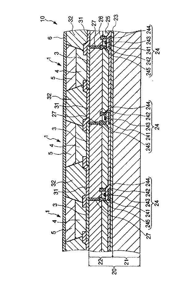
The
基体20は、基板21と、この基板21上に形成された回路部22とを有している。
回路部22は、基板21上に形成された、例えば酸化シリコン層からなる保護層23と、保護層23上に形成された駆動用TFT(スイッチング素子)24と、第1層間絶縁層25と、第2層間絶縁層26とを有している。
駆動用TFT24は、シリコンからなる半導体層241と、半導体層241上に形成されたゲート絶縁層242と、ゲート絶縁層242上に形成されたゲート電極243と、ソース電極244と、ドレイン電極245とを有している。
このような回路部22上に、各駆動用TFT24に対応して、それぞれ、発光素子1が設けられている。また、隣接する発光素子1同士は、第1隔壁部31および第2隔壁部32により区画されている。
The
The circuit unit 22 includes a
The driving
On such a circuit portion 22, the light emitting element 1 is provided corresponding to each driving
本実施形態では、各発光素子1の陽極3は、画素電極を構成し、各駆動用TFT24のドレイン電極245に配線27により電気的に接続されている。また、各発光素子1の陰極6は、共通電極とされている。
そして、各発光素子1を覆うように封止部材(図示せず)が基体20に接合され、各発光素子1が封止されている。
ディスプレイ装置10は、単色表示であってもよく、各発光素子1に用いる発光材料を選択することにより、カラー表示も可能である。
このようなディスプレイ装置10(表示装置)は、各種の電子機器に組み込むことができる。
In the present embodiment, the
Then, a sealing member (not shown) is bonded to the base 20 so as to cover each light emitting element 1, and each light emitting element 1 is sealed.
The
Such a display device 10 ( display device ) can be incorporated into various electronic devices.
図5は、電子機器を適用したモバイル型(またはノート型)のパーソナルコンピュータの構成を示す斜視図である。
この図において、パーソナルコンピュータ1100は、キーボード1102を備えた本体部1104と、表示部を備える表示ユニット1106とにより構成され、表示ユニット1106は、本体部1104に対しヒンジ構造部を介して回動可能に支持されている。
このパーソナルコンピュータ1100において、表示ユニット1106が備える表示部が前述のディスプレイ装置10で構成されている。
FIG. 5 is a perspective view illustrating a configuration of a mobile (or notebook) personal computer to which an electronic device is applied.
In this figure, a
In the
図6は、電子機器を適用した携帯電話機(PHSも含む)の構成を示す斜視図である。
この図において、携帯電話機1200は、複数の操作ボタン1202、受話口1204および送話口1206とともに、表示部を備えている。
携帯電話機1200において、この表示部が前述のディスプレイ装置10で構成されている。
FIG. 6 is a perspective view illustrating a configuration of a mobile phone (including PHS) to which an electronic device is applied.
In this figure, a
In the
図7は、電子機器を適用したディジタルスチルカメラの構成を示す斜視図である。なお、この図には、外部機器との接続についても簡易的に示されている。
ここで、通常のカメラは、被写体の光像により銀塩写真フィルムを感光するのに対し、ディジタルスチルカメラ1300は、被写体の光像をCCD(Charge Coupled Device)などの撮像素子により光電変換して撮像信号(画像信号)を生成する。
FIG. 7 is a perspective view illustrating a configuration of a digital still camera to which an electronic device is applied. In this figure, connection with an external device is also simply shown.
Here, an ordinary camera sensitizes a silver halide photographic film with a light image of a subject, whereas a
ディジタルスチルカメラ1300におけるケース(ボディー)1302の背面には、表示部が設けられ、CCDによる撮像信号に基づいて表示を行う構成になっており、被写体を電子画像として表示するファインダとして機能する。
ディジタルスチルカメラ1300において、この表示部が前述のディスプレイ装置10で構成されている。
A display unit is provided on the back of a case (body) 1302 in the
In the
ケースの内部には、回路基板1308が設置されている。この回路基板1308は、撮像信号を格納(記憶)し得るメモリが設置されている。
また、ケース1302の正面側(図示の構成では裏面側)には、光学レンズ(撮像光学系)やCCDなどを含む受光ユニット1304が設けられている。
撮影者が表示部に表示された被写体像を確認し、シャッタボタン1306を押下すると、その時点におけるCCDの撮像信号が、回路基板1308のメモリに転送・格納される。
A
A
When the photographer confirms the subject image displayed on the display unit and presses the
また、このディジタルスチルカメラ1300においては、ケース1302の側面に、ビデオ信号出力端子1312と、データ通信用の入出力端子1314とが設けられている。そして、図示のように、ビデオ信号出力端子1312にはテレビモニタ1430が、デ−タ通信用の入出力端子1314にはパーソナルコンピュータ1440が、それぞれ必要に応じて接続される。さらに、所定の操作により、回路基板1308のメモリに格納された撮像信号が、テレビモニタ1430や、パーソナルコンピュータ1440に出力される構成になっている。
In the
なお、電子機器は、図5のパーソナルコンピュータ(モバイル型パーソナルコンピュータ)、図6の携帯電話機、図7のディジタルスチルカメラの他にも、例えば、テレビや、ビデオカメラ、ビューファインダ型、モニタ直視型のビデオテープレコーダ、ラップトップ型パーソナルコンピュータ、カーナビゲーション装置、ページャ、電子手帳(通信機能付も含む)、電子辞書、電卓、電子ゲーム機器、ワードプロセッサ、ワークステーション、テレビ電話、防犯用テレビモニタ、電子双眼鏡、POS端末、タッチパネルを備えた機器(例えば金融機関のキャッシュディスペンサー、自動券売機)、医療機器(例えば電子体温計、血圧計、血糖計、心電表示装置、超音波診断装置、内視鏡用表示装置)、魚群探知機、各種測定機器、計器類(例えば、車両、航空機、船舶の計器類)、フライトシュミレータ、その他各種モニタ類、プロジェクター等の投射型表示装置等に適用することができる。
以上、本発明の発光素子の製造方法を、図示の実施形態に基づいて説明したが、本発明はこれらに限定されるものでない。
In addition to the personal computer (mobile personal computer) shown in FIG. 5, the mobile phone shown in FIG. 6, and the digital still camera shown in FIG. 7, the electronic apparatus may be, for example, a television, a video camera, a viewfinder type, or a monitor direct view type. Video tape recorders, laptop personal computers, car navigation devices, pagers, electronic notebooks (including those with communication functions), electronic dictionaries, calculators, electronic game machines, word processors, workstations, videophones, security TV monitors, electronic Devices equipped with binoculars, POS terminals, touch panels (for example, cash dispensers of financial institutions, automatic ticket vending machines), medical devices (for example, electronic thermometers, blood pressure monitors, blood glucose meters, electrocardiographs, ultrasonic diagnostic devices, endoscopes) Display device), fish finder, various measuring instruments, instruments ( In example, gages for vehicles, aircraft, ships), a flight simulator, various monitors, and a projection display such as a projector.
As mentioned above, although the manufacturing method of the light emitting element of this invention was demonstrated based on embodiment of illustration, this invention is not limited to these.
次に、本発明の具体的実施例について説明する。
(実施例1)
以下に示すようにして発光素子を製造し、それらの発光効率および耐久性(寿命)について評価した。
Next, specific examples of the present invention will be described.
Example 1
Light emitting elements were manufactured as shown below, and their light emission efficiency and durability (lifetime) were evaluated.
[サンプルNo.1A]
(1A) まず、平均厚さ0.5mmの透明なガラス基板を用意した。
(2A) 次に、この基板上に、スパッタ法により、平均厚さ100nmのITO電極(陽極)を形成した。
(3A) 次に、このITO電極上に、0.1wt%のNH2(CH2)5SiCl3(シランカップリング剤)のエタノール溶液をスピンコート法(2000rpm)により塗布した後、乾燥した。
[Sample No. 1A]
(1A) First, a transparent glass substrate having an average thickness of 0.5 mm was prepared.
(2A) Next, an ITO electrode (anode) having an average thickness of 100 nm was formed on the substrate by sputtering.
(3A) Next, an ethanol solution of 0.1 wt% NH 2 (CH 2 ) 5 SiCl 3 (silane coupling agent) was applied on the ITO electrode by a spin coating method (2000 rpm) and then dried.
(4A) 次に、第1の有機ポリマーとして、前記化1に示すポリフェニルアミン系高分子(重量平均分子量:40000)と、第2の有機ポリマーとして、前記化2に示すポリフルオレン系高分子(重量平均分子量:5000)と、発光層の構成材料として、イリジウム錯体で被覆した酸化ジルコニウム粒子とを、それぞれ、キシレンに添加して液状材料を調製した。 (4A) Next, as the first organic polymer, the polyphenylamine-based polymer (weight average molecular weight: 40000) shown in Chemical Formula 1 and as the second organic polymer, the polyfluorene-based polymer shown in Chemical Formula 2 A liquid material was prepared by adding (weight average molecular weight: 5000) and zirconium oxide particles coated with an iridium complex as constituent materials of the light-emitting layer to xylene.
なお、ポリフェニルアミン系高分子の含有量は、0.5wt%、ポリフルオレン系高分子の含有量は、0.5wt%、また、イリジウム錯体で被覆した酸化ジルコニウム粒子の含有量は、2.0wt%とした。
また、酸化ジルコニウム粒子の平均粒径は、5nmのものを用いた。
また、イリジウム錯体には、前記化3に示す2,2’−ビピリジン−4,4’−ジカルボン酸を配位子に持つ、3配位のイリジウム錯体を用いた。
The polyphenylamine polymer content is 0.5 wt%, the polyfluorene polymer content is 0.5 wt%, and the zirconium oxide particles coated with the iridium complex are 2. It was 0 wt%.
The average particle diameter of the zirconium oxide particles was 5 nm.
As the iridium complex, a tricoordinate iridium complex having 2,2′-bipyridine-4,4′-dicarboxylic acid represented by
そして、この液状材料をITO電極上に、スピンコート法(2000rpm)により塗布した後、乾燥した。これにより、正孔輸送層(第1の領域および第2の領域)と発光層とを相分離により形成した。
なお、液状材料の乾燥条件は、イソプロパノール雰囲気中、50℃とした。なお、この温度は、液状被膜中に対流が生じる温度である。
And this liquid material was apply | coated by the spin coat method (2000 rpm) on the ITO electrode, Then, it dried. Thereby, the hole transport layer (the first region and the second region) and the light emitting layer were formed by phase separation.
The drying conditions for the liquid material were 50 ° C. in an isopropanol atmosphere. This temperature is a temperature at which convection occurs in the liquid film.
(5A) 次に、中間層の構成材料として、F17(フッ化炭素系シランカップリング化合物)で被覆した酸化ジルコニウム粒子をイソプロパノールに分散して分散液を調製した。
そして、この分散液を発光層上に、スピンコート法(2000rpm)により塗布した後、乾燥した。これにより、平均厚さ10nmの中間層を形成した。
なお、酸化ジルコニウム粒子の平均粒径は、5nmのものを用いた。
(6A) 次に、中間層上に、真空蒸着法により、平均厚さ300nmのAlLi電極(陰極)を形成した。
次に、形成した各層を覆うように、ポリカーボネート製の保護カバー(封止部材)を被せ、紫外線硬化性樹脂により固定、封止して、発光素子を完成した。
[サンプルNo.2A]
前記工程(3A)において、下記化4に示すシランカップリング剤を用いた以外は、前記サンプルNo.1Aと同様にして発光素子を製造した。
(5A) Next, as a constituent material of the intermediate layer, zirconium oxide particles coated with F17 (fluorocarbon-based silane coupling compound) were dispersed in isopropanol to prepare a dispersion.
And this dispersion liquid was apply | coated by the spin coat method (2000 rpm) on the light emitting layer, Then, it dried. Thereby, an intermediate layer having an average thickness of 10 nm was formed.
The average particle diameter of zirconium oxide particles was 5 nm.
(6A) Next, an AlLi electrode (cathode) having an average thickness of 300 nm was formed on the intermediate layer by vacuum deposition.
Next, a polycarbonate protective cover (sealing member) was placed so as to cover each formed layer, and fixed and sealed with an ultraviolet curable resin to complete a light emitting element.
[Sample No. 2A]
In the step (3A), the sample No. 1 was used except that the silane coupling agent shown in the following chemical formula 4 was used. A light emitting device was manufactured in the same manner as 1A.
[サンプルNo.3A]
前記工程(3A)を省略した以外は、前記サンプルNo.1Aと同様にして発光素子を製造した。
そして、サンプルNo.1A〜3Aの発光素子について、それぞれ、発光効率および寿命の評価を行った。
[Sample No. 3A]
Except for omitting the step (3A), the sample no. A light emitting device was manufactured in the same manner as 1A.
And sample no. The light emitting elements 1A to 3A were evaluated for light emission efficiency and lifetime.
この発光効率の評価は、直流電源により、0Vから6Vに電圧を印加し、電流値を測定し、輝度を輝度計により測定することで行った。また、寿命の評価は、初期輝度400cd/m2の定電流駆動を行うことで行った。
その結果、サンプルNo.1Aおよび2Aの発光素子(本発明)は、いずれも、その発光効率が、サンプルNo.3A(比較例)の発光効率に対して、約1.3倍上昇するのが確認された。
The luminous efficiency was evaluated by applying a voltage from 0 V to 6 V with a DC power source, measuring the current value, and measuring the luminance with a luminance meter. In addition, the evaluation of the lifetime was performed by performing constant current driving with an initial luminance of 400 cd / m 2 .
As a result, sample no. Each of the light emitting elements 1A and 2A (the present invention) has a luminous efficiency of Sample No. It was confirmed that the luminous efficiency of 3A (comparative example) rose about 1.3 times.
また、サンプルNo.1Aおよび2Aの発光素子(本発明)は、いずれも、その輝度の半減期が、サンプルNo.3A(比較例)の輝度の半減期に対して、約1.5倍延長することが確認された。
また、第1の有機ポリマーをポリアリールアミン、フルオレン−アリールアミン共重合体またはこれらの誘導体から選択し、第2の有機ポリマーをポリフルオレン、フルオレン−ビチオフェン共重合体またはこれらの誘導体から選択して組み合わせて、前記と同様にして発光素子を製造すると、前記と同様の結果が得られる。
Sample No. Both of the light emitting elements 1A and 2A (the present invention) have a luminance half-life of Sample No. It was confirmed that the luminance half-life of 3A (comparative example) was extended by about 1.5 times.
In addition, the first organic polymer is selected from polyarylamine, fluorene-arylamine copolymer or derivatives thereof, and the second organic polymer is selected from polyfluorene, fluorene-bithiophene copolymer or derivatives thereof. When combined and manufactured in the same manner as described above, the same result as described above can be obtained.
(実施例2)
以下に示すようにして、各サンプルNo.の評価対象物を、それぞれ5個ずつ作製し、各層の分離状態を確認するとともに、膜厚を測定した。
[サンプルNo.1B]
前記サンプルNo.1Aにおける工程(1A)〜(4A)と同様の工程を行って、評価対象物を作製した。
[サンプルNo.2B]
前記サンプルNo.2Aにおける工程(1A)〜(4A)と同様の工程を行って、評価対象物を作製した。
(Example 2)
As shown below, each sample No. Five evaluation objects were prepared, and the separation state of each layer was confirmed, and the film thickness was measured.
[Sample No. 1B]
Sample No. The same processes as those in steps (1A) to (4A) in 1A were performed to produce an evaluation object.
[Sample No. 2B]
Sample No. Processes similar to the processes (1A) to (4A) in 2A were performed to produce an evaluation object.
[サンプルNo.3B]
前記サンプルNo.3Aにおける工程(1A)〜(4A)と同様の工程を行って、評価対象物を作製した。
そして、サンプルNo.1B〜3Bの評価対象物について、それぞれ、第1の領域、第2の領域および発光層の各層の分離状態を確認するとともに、膜厚を測定した。
これは、第1の領域、第2の領域および発光層の積層体を、発光層側からピンで引っかき、剥離した部分を蛍光顕微鏡(オリンパス社製、「BX50」)で観察した後、段差計(テンコール社製、「P−10」)で計測することにより行った。
[Sample No. 3B]
Sample No. The same process as 3A process (1A)-(4A) was performed, and the evaluation target was produced.
And sample no. Regarding the evaluation objects 1B to 3B, the separation state of each of the first region, the second region, and the light emitting layer was confirmed, and the film thickness was measured.
This is because the laminate of the first region, the second region and the light emitting layer is scratched with a pin from the light emitting layer side, and the peeled portion is observed with a fluorescence microscope (OLYMPUS, “BX50”), (Tencor company make, "P-10").
各層の膜厚の測定結果は、次に示す通りである。なお、各層の膜厚の値は、5個の平均値である。
・サンプルNo.1B(本発明に相当)
第1の領域:33nm、第2の領域:35nm、発光層:22nm
・サンプルNo.2B(本発明に相当)
第1の領域:35nm、第2の領域:34nm、発光層:20nm
・サンプルNo.3B(比較例に相当)
第1の領域:28nm、第2の領域:45nm、発光層:18nm
The measurement results of the thickness of each layer are as follows. In addition, the value of the film thickness of each layer is an average value of five.
・ Sample No. 1B (corresponding to the present invention)
First region: 33 nm, second region: 35 nm, light emitting layer: 22 nm
・ Sample No. 2B (equivalent to the present invention)
First region: 35 nm, second region: 34 nm, light emitting layer: 20 nm
・ Sample No. 3B (equivalent to comparative example)
First region: 28 nm, second region: 45 nm, light emitting layer: 18 nm
サンプルNo.1Bおよび2Bの評価対象物では、いずれも、蛍光顕微鏡の観察ではっきりとした段差が確認でき、膜厚の測定結果においても、各層がほぼ目的とする膜厚に形成されていた。
これに対して、サンプルNo.3Bの評価対象物では、いずれも、蛍光顕微鏡の観察で段差が確認できたものの、その段差がはっきりしないものがあり、膜厚の測定結果においても、各層が目的とする膜厚から大きくズレていた。
Sample No. In each of the evaluation objects 1B and 2B, a clear step can be confirmed by observation with a fluorescence microscope, and each layer is formed to have a substantially desired film thickness in the film thickness measurement result.
In contrast, sample no. In all the evaluation objects of 3B, although the level difference was confirmed by observation with a fluorescence microscope, the level difference was not clear. In the measurement result of the film thickness, each layer was greatly deviated from the target film thickness. It was.
これらの結果から、親和性向上処理を施すことにより、より確実な相分離が可能となることが明らかとなった。また、これらの結果が、前記実施例1で示したような発光素子の特性の向上に反映されたもと推察される。
また、親和性向上処理に用いるシランカップリング剤の種類を代えて、前記と同様にして評価対象物を作製したところ、各層の分離状態を変化させ得ることが確認された。
From these results, it has been clarified that more reliable phase separation can be achieved by the affinity improvement treatment. In addition, these results are presumed based on the improvement of the characteristics of the light emitting element as shown in Example 1.
Moreover, when the evaluation object was produced similarly to the above, changing the kind of silane coupling agent used for an affinity improvement process, it was confirmed that the isolation | separation state of each layer can be changed.
1……発光素子 2……基板 3……陽極 4……正孔輸送層 41……第1の領域 42……第2の領域 5……発光層 51……無機半導体粒子 52……発光材料 6……陰極 7……封止部材 10……ディスプレイ装置 20……基体 21……基板 22……回路部 23……保護層 24……駆動用TFT 241……半導体層 242……ゲート絶縁層 243……ゲート電極 244……ソース電極 245……ドレイン電極 25……第1層間絶縁層 26……第2層間絶縁層 27……配線 31……第1隔壁部 32……第2隔壁部 1100……パーソナルコンピュータ 1102……キーボード 1104……本体部 1106……表示ユニット 1200……携帯電話機 1202……操作ボタン 1204……受話口 1206……送話口 1300‥‥ディジタルスチルカメラ 1302‥‥ケース(ボディー) 1304‥‥受光ユニット 1306‥‥シャッタボタン 1308‥‥回路基板 1312‥‥ビデオ信号出力端子 1314‥‥データ通信用の入出力端子 1430‥‥テレビモニタ 1440‥‥パーソナルコンピュータ
DESCRIPTION OF SYMBOLS 1 ...
Claims (13)
前記一対の電極のうち、一方の電極の前記キャリア輸送層を形成する面側に、前記有機ポリマーとの親和性を向上させるための親和性向上処理を施す第1の工程と、
前記複合体と前記有機ポリマーと非極性溶媒とを含有する液状材料を、前記一方の電極の前記キャリア輸送層を形成する面側に供給して液状被膜を形成し、極性溶媒の蒸気を含有する雰囲気中で、前記液状被膜中から前記非極性溶媒を除去しつつ、前記有機ポリマーを前記一方の電極側に、前記複合体を他方の電極側に分離して、前記キャリア輸送層と前記発光層とを一括して形成する第2の工程とを有することを特徴とする発光素子の製造方法。 Between a pair of electrodes, a light-emitting layer composed of a composite formed by coating at least a part of inorganic semiconductor particles with a light-emitting material, and a carrier transport layer composed of an organic polymer in contact with the light-emitting layer A method of manufacturing a light emitting device for manufacturing a light emitting device interposed,
A first step of performing an affinity improvement treatment for improving the affinity with the organic polymer on a surface side of the pair of electrodes on which the carrier transport layer is formed;
A liquid material containing the composite, the organic polymer, and a nonpolar solvent is supplied to the surface of the one electrode on which the carrier transport layer is formed to form a liquid film, which contains polar solvent vapor. In the atmosphere, while removing the nonpolar solvent from the liquid film, separating the organic polymer on the one electrode side and separating the complex on the other electrode side, the carrier transport layer and the light emitting layer And a second step of collectively forming the light emitting element.
前記第1の工程における前記親和性向上処理では、前記一方の電極の前記発光層を形成する面側に、前記第1の有機ポリマーとの親和性を向上させる処理を行う請求項3に記載の発光素子の製造方法。 The hole transport layer includes a first region composed of a first organic polymer on the one electrode side, and a second organic polymer of a type different from the first organic polymer on the light emitting layer side. A second region composed of
The said affinity improvement process in a said 1st process WHEREIN: The process which improves the affinity with a said 1st organic polymer is performed to the surface side which forms the said light emitting layer of said one electrode. Manufacturing method of light emitting element.
Priority Applications (5)
| Application Number | Priority Date | Filing Date | Title |
|---|---|---|---|
| JP2005008407A JP4450207B2 (en) | 2005-01-14 | 2005-01-14 | Method for manufacturing light emitting device |
| KR1020050116239A KR100720051B1 (en) | 2005-01-14 | 2005-12-01 | Method of manufacturing light-emitting element, light-emitting element, display device and electronic equipment |
| CNB2006100036189A CN100573967C (en) | 2005-01-14 | 2006-01-09 | The manufacture method of light-emitting component, light-emitting component, display unit and electronic instrument |
| EP06000572A EP1681735A2 (en) | 2005-01-14 | 2006-01-12 | Method of manufacturing a light-emitting element, light-emitting element, display device and electronic equipment |
| US11/331,236 US7591699B2 (en) | 2005-01-14 | 2006-01-13 | Method of manufacturing light-emitting element including the emission layer and the carrier transfer layer |
Applications Claiming Priority (1)
| Application Number | Priority Date | Filing Date | Title |
|---|---|---|---|
| JP2005008407A JP4450207B2 (en) | 2005-01-14 | 2005-01-14 | Method for manufacturing light emitting device |
Publications (2)
| Publication Number | Publication Date |
|---|---|
| JP2006196376A JP2006196376A (en) | 2006-07-27 |
| JP4450207B2 true JP4450207B2 (en) | 2010-04-14 |
Family
ID=36168541
Family Applications (1)
| Application Number | Title | Priority Date | Filing Date |
|---|---|---|---|
| JP2005008407A Expired - Fee Related JP4450207B2 (en) | 2005-01-14 | 2005-01-14 | Method for manufacturing light emitting device |
Country Status (5)
| Country | Link |
|---|---|
| US (1) | US7591699B2 (en) |
| EP (1) | EP1681735A2 (en) |
| JP (1) | JP4450207B2 (en) |
| KR (1) | KR100720051B1 (en) |
| CN (1) | CN100573967C (en) |
Families Citing this family (14)
| Publication number | Priority date | Publication date | Assignee | Title |
|---|---|---|---|---|
| US8138075B1 (en) | 2006-02-06 | 2012-03-20 | Eberlein Dietmar C | Systems and methods for the manufacture of flat panel devices |
| JP4952906B2 (en) * | 2006-11-15 | 2012-06-13 | ソニーケミカル&インフォメーションデバイス株式会社 | Encapsulating resin composition and light emitting device |
| JP2008140620A (en) * | 2006-11-30 | 2008-06-19 | Optrex Corp | Organic electroluminescent device and manufacturing method of same |
| TW200847452A (en) * | 2007-05-23 | 2008-12-01 | Wang yong qi | Photovoltaic cell and its red light conversion layer |
| KR100835059B1 (en) * | 2007-07-06 | 2008-06-03 | 삼성전자주식회사 | Quantum dot optical device |
| KR20110055563A (en) | 2008-07-30 | 2011-05-25 | 스미또모 가가꾸 가부시키가이샤 | Laminated structure, manufacturing method thereof, and electronic device comprising same |
| US20110095271A1 (en) * | 2009-10-27 | 2011-04-28 | Donal Donat Conor Bradley | Hybrid organic light emitting device |
| US8947415B1 (en) | 2010-04-19 | 2015-02-03 | Green Display LLC | Display system and method |
| KR101244926B1 (en) * | 2011-04-28 | 2013-03-18 | 피에스아이 주식회사 | Micro LED device and manufacturing method thereof |
| KR101209449B1 (en) | 2011-04-29 | 2012-12-07 | 피에스아이 주식회사 | Full-color LED display device and manufacturing method thereof |
| KR101936978B1 (en) * | 2011-07-05 | 2019-01-09 | 닛산 가가쿠 가부시키가이샤 | Vertically phase-separating semiconducting organic material layers |
| JP6136366B2 (en) * | 2013-02-28 | 2017-05-31 | 日立化成株式会社 | Organic electronic device and method for manufacturing the same |
| CN105541855B (en) * | 2015-11-25 | 2018-08-07 | 内蒙古自治区科学技术研究院有限责任公司东部分院 | A kind of 1,8- naphthalimide compounds being bonded with spiro-pyrans and preparation method and application |
| CN110350096A (en) * | 2019-06-27 | 2019-10-18 | 深圳市华星光电半导体显示技术有限公司 | A kind of Ca-Ti ore type electroluminescent device and preparation method thereof |
Family Cites Families (22)
| Publication number | Priority date | Publication date | Assignee | Title |
|---|---|---|---|---|
| KR100697861B1 (en) * | 1998-03-13 | 2007-03-22 | 캠브리지 디스플레이 테크놀로지 리미티드 | Electric field light emitting devices |
| GB9805476D0 (en) * | 1998-03-13 | 1998-05-13 | Cambridge Display Tech Ltd | Electroluminescent devices |
| US6329017B1 (en) * | 1998-12-23 | 2001-12-11 | Battelle Memorial Institute | Mesoporous silica film from a solution containing a surfactant and methods of making same |
| JP4043135B2 (en) * | 1999-03-29 | 2008-02-06 | 株式会社東芝 | Functional element and multi-component multi-phase polymer molding |
| US6625901B1 (en) * | 1999-05-27 | 2003-09-30 | Oliver Design, Inc. | Apparatus and method for drying a thin substrate |
| US7288420B1 (en) * | 1999-06-04 | 2007-10-30 | Semiconductor Energy Laboratory Co., Ltd. | Method for manufacturing an electro-optical device |
| EP1244723B1 (en) * | 2000-01-05 | 2004-11-24 | Cambridge Display Technology Limited | Luminescent polymer |
| US6512082B2 (en) * | 2000-01-05 | 2003-01-28 | Cambridge Display Technology Ltd. | Polymers, their preparation and uses |
| GB0004541D0 (en) * | 2000-02-25 | 2000-04-19 | Cambridge Display Tech Ltd | Luminescent polymer |
| US6887973B2 (en) * | 2000-02-25 | 2005-05-03 | Cambridge Display Technology Limited | Electro-luminescent polymers, their preparation and uses |
| US6858324B2 (en) * | 2000-03-10 | 2005-02-22 | Cambridge Display Technology Limited | Copolymer |
| KR100495407B1 (en) * | 2001-08-20 | 2005-06-14 | 티디케이가부시기가이샤 | Organic EL Device and Preparation Method |
| TW563088B (en) * | 2001-09-17 | 2003-11-21 | Semiconductor Energy Lab | Light emitting device, method of driving a light emitting device, and electronic equipment |
| JP2003115377A (en) | 2001-10-03 | 2003-04-18 | Nec Corp | Light emitting device, method of manufacturing the same, and display device using the same |
| JP4281342B2 (en) * | 2001-12-05 | 2009-06-17 | セイコーエプソン株式会社 | Pattern forming method and wiring forming method |
| US6876143B2 (en) * | 2002-11-19 | 2005-04-05 | John James Daniels | Organic light active devices and methods for fabricating the same |
| EP1388903B1 (en) * | 2002-08-09 | 2016-03-16 | Semiconductor Energy Laboratory Co., Ltd. | Organic electroluminescent device |
| JP4289852B2 (en) * | 2002-09-18 | 2009-07-01 | 大日本印刷株式会社 | Method for manufacturing electroluminescent device |
| US20060134317A1 (en) * | 2003-02-03 | 2006-06-22 | Yang Yang | Method for making multifunctional organic thin films |
| US7906224B2 (en) * | 2003-08-21 | 2011-03-15 | Konica Minolta Holdings, Inc. | Organic electroluminescent device, display, and illuminating device |
| JP2005085604A (en) * | 2003-09-09 | 2005-03-31 | Seiko Epson Corp | Organic metal compound thin film forming method, organic metal compound thin film, and manufacturing method of organic electronic device including the same, organic electronic device, manufacturing method of organic electroluminescence, organic electroluminescence, and electronic apparatus |
| US20060142520A1 (en) * | 2004-12-27 | 2006-06-29 | 3M Innovative Properties Company | Hole transport layers for organic electroluminescent devices |
-
2005
- 2005-01-14 JP JP2005008407A patent/JP4450207B2/en not_active Expired - Fee Related
- 2005-12-01 KR KR1020050116239A patent/KR100720051B1/en not_active Expired - Fee Related
-
2006
- 2006-01-09 CN CNB2006100036189A patent/CN100573967C/en not_active Expired - Fee Related
- 2006-01-12 EP EP06000572A patent/EP1681735A2/en not_active Withdrawn
- 2006-01-13 US US11/331,236 patent/US7591699B2/en not_active Expired - Fee Related
Also Published As
| Publication number | Publication date |
|---|---|
| KR100720051B1 (en) | 2007-05-18 |
| JP2006196376A (en) | 2006-07-27 |
| CN1819304A (en) | 2006-08-16 |
| EP1681735A2 (en) | 2006-07-19 |
| US7591699B2 (en) | 2009-09-22 |
| KR20060083119A (en) | 2006-07-20 |
| US20060158106A1 (en) | 2006-07-20 |
| CN100573967C (en) | 2009-12-23 |
Similar Documents
| Publication | Publication Date | Title |
|---|---|---|
| JP4450207B2 (en) | Method for manufacturing light emitting device | |
| JP4244941B2 (en) | LIGHT EMITTING ELEMENT, LIGHT EMITTING DEVICE, AND ELECTRONIC DEVICE | |
| JP2007053286A (en) | LIGHT EMITTING ELEMENT, DISPLAY DEVICE, AND ELECTRONIC DEVICE | |
| JP2009070954A (en) | ORGANIC THIN-FILM LIGHT EMITTING ELEMENT, DISPLAY DEVICE, ELECTRONIC DEVICE, AND METHOD FOR MANUFACTURING ORGANIC THIN FILM LIGHT-EMITTING ELEMENT | |
| JP4548121B2 (en) | Method for manufacturing light emitting device | |
| JP4311360B2 (en) | LIGHT EMITTING ELEMENT, LIGHT EMITTING DEVICE, AND ELECTRONIC DEVICE | |
| JP4277816B2 (en) | LIGHT EMITTING ELEMENT, DISPLAY DEVICE, AND ELECTRONIC DEVICE | |
| JP4305425B2 (en) | Electronic devices and electronic equipment | |
| JP2008258198A (en) | LIGHT EMITTING ELEMENT, LIGHT EMITTING DEVICE, AND ELECTRONIC DEVICE | |
| JP4534875B2 (en) | LIGHT EMITTING ELEMENT, LIGHT EMITTING ELEMENT MANUFACTURING METHOD, ELECTRONIC DEVICE, AND ELECTRONIC DEVICE | |
| JP4867169B2 (en) | Conductive polymer, conductive layer, electronic device and electronic equipment | |
| JP2008283020A (en) | LIGHT EMITTING ELEMENT, DISPLAY DEVICE, AND ELECTRONIC DEVICE | |
| JP2006245178A (en) | Composition for conductive material, conductive material, conductive layer, electronic device and electronic apparatus | |
| JP4715329B2 (en) | Manufacturing method of substrate for electronic device | |
| JP4311380B2 (en) | Electronic device substrate, method for manufacturing electronic device substrate, electronic device and electronic apparatus | |
| JP4457947B2 (en) | Composition for conductive material, conductive material, conductive layer, electronic device and electronic apparatus | |
| JP2006245261A (en) | Composition for conductive material, conductive material, conductive layer, electronic device and electronic apparatus | |
| JP2006241267A (en) | Composition for conductive material, conductive material, conductive layer, electronic device and electronic apparatus | |
| JP2006199909A (en) | Composition for conductive material, conductive material, conductive layer, electronic device and electronic apparatus | |
| JP2006193706A (en) | Composition for conductive material, conductive material, conductive layer, electronic device and electronic apparatus | |
| JP2006241266A (en) | Composition for conductive material, conductive material, conductive layer, electronic device and electronic apparatus | |
| JP2006237442A (en) | Composition for conductive material, conductive material, conductive layer, electronic device and electronic apparatus | |
| JP2007207961A (en) | Electronic device substrate, electronic device and electronic equipment | |
| JP2006193542A (en) | Conductive polymer, conductive layer, electronic device and electronic equipment | |
| JP2006213905A (en) | Conductive material, composition for conductive material, conductive layer, electronic device and electronic apparatus |
Legal Events
| Date | Code | Title | Description |
|---|---|---|---|
| A977 | Report on retrieval |
Free format text: JAPANESE INTERMEDIATE CODE: A971007 Effective date: 20080827 |
|
| A131 | Notification of reasons for refusal |
Free format text: JAPANESE INTERMEDIATE CODE: A131 Effective date: 20080902 |
|
| A521 | Request for written amendment filed |
Free format text: JAPANESE INTERMEDIATE CODE: A523 Effective date: 20081031 |
|
| A131 | Notification of reasons for refusal |
Free format text: JAPANESE INTERMEDIATE CODE: A131 Effective date: 20091006 |
|
| A521 | Request for written amendment filed |
Free format text: JAPANESE INTERMEDIATE CODE: A523 Effective date: 20091203 |
|
| TRDD | Decision of grant or rejection written | ||
| A01 | Written decision to grant a patent or to grant a registration (utility model) |
Free format text: JAPANESE INTERMEDIATE CODE: A01 Effective date: 20100106 |
|
| A01 | Written decision to grant a patent or to grant a registration (utility model) |
Free format text: JAPANESE INTERMEDIATE CODE: A01 |
|
| R150 | Certificate of patent or registration of utility model |
Free format text: JAPANESE INTERMEDIATE CODE: R150 |
|
| A61 | First payment of annual fees (during grant procedure) |
Free format text: JAPANESE INTERMEDIATE CODE: A61 Effective date: 20100119 |
|
| FPAY | Renewal fee payment (event date is renewal date of database) |
Free format text: PAYMENT UNTIL: 20130205 Year of fee payment: 3 |
|
| FPAY | Renewal fee payment (event date is renewal date of database) |
Free format text: PAYMENT UNTIL: 20130205 Year of fee payment: 3 |
|
| S531 | Written request for registration of change of domicile |
Free format text: JAPANESE INTERMEDIATE CODE: R313531 |
|
| R350 | Written notification of registration of transfer |
Free format text: JAPANESE INTERMEDIATE CODE: R350 |
|
| LAPS | Cancellation because of no payment of annual fees |