JP4419049B2 - Memory module and memory system - Google Patents
Memory module and memory system Download PDFInfo
- Publication number
- JP4419049B2 JP4419049B2 JP2003115834A JP2003115834A JP4419049B2 JP 4419049 B2 JP4419049 B2 JP 4419049B2 JP 2003115834 A JP2003115834 A JP 2003115834A JP 2003115834 A JP2003115834 A JP 2003115834A JP 4419049 B2 JP4419049 B2 JP 4419049B2
- Authority
- JP
- Japan
- Prior art keywords
- chip
- dram
- signal
- memory
- memory module
- Prior art date
- Legal status (The legal status is an assumption and is not a legal conclusion. Google has not performed a legal analysis and makes no representation as to the accuracy of the status listed.)
- Expired - Fee Related
Links
Images


Classifications
-
- G—PHYSICS
- G11—INFORMATION STORAGE
- G11C—STATIC STORES
- G11C11/00—Digital stores characterised by the use of particular electric or magnetic storage elements; Storage elements therefor
- G11C11/21—Digital stores characterised by the use of particular electric or magnetic storage elements; Storage elements therefor using electric elements
- G11C11/34—Digital stores characterised by the use of particular electric or magnetic storage elements; Storage elements therefor using electric elements using semiconductor devices
- G11C11/40—Digital stores characterised by the use of particular electric or magnetic storage elements; Storage elements therefor using electric elements using semiconductor devices using transistors
- G11C11/401—Digital stores characterised by the use of particular electric or magnetic storage elements; Storage elements therefor using electric elements using semiconductor devices using transistors forming cells needing refreshing or charge regeneration, i.e. dynamic cells
- G11C11/4063—Auxiliary circuits, e.g. for addressing, decoding, driving, writing, sensing or timing
- G11C11/407—Auxiliary circuits, e.g. for addressing, decoding, driving, writing, sensing or timing for memory cells of the field-effect type
- G11C11/408—Address circuits
-
- F—MECHANICAL ENGINEERING; LIGHTING; HEATING; WEAPONS; BLASTING
- F24—HEATING; RANGES; VENTILATING
- F24C—DOMESTIC STOVES OR RANGES ; DETAILS OF DOMESTIC STOVES OR RANGES, OF GENERAL APPLICATION
- F24C15/00—Details
- F24C15/20—Removing cooking fumes
- F24C15/2035—Arrangement or mounting of filters
-
- G—PHYSICS
- G11—INFORMATION STORAGE
- G11C—STATIC STORES
- G11C5/00—Details of stores covered by group G11C11/00
-
- G—PHYSICS
- G11—INFORMATION STORAGE
- G11C—STATIC STORES
- G11C29/00—Checking stores for correct operation ; Subsequent repair; Testing stores during standby or offline operation
- G11C29/04—Detection or location of defective memory elements, e.g. cell constructio details, timing of test signals
- G11C29/08—Functional testing, e.g. testing during refresh, power-on self testing [POST] or distributed testing
- G11C29/12—Built-in arrangements for testing, e.g. built-in self testing [BIST] or interconnection details
- G11C29/1201—Built-in arrangements for testing, e.g. built-in self testing [BIST] or interconnection details comprising I/O circuitry
-
- G—PHYSICS
- G11—INFORMATION STORAGE
- G11C—STATIC STORES
- G11C29/00—Checking stores for correct operation ; Subsequent repair; Testing stores during standby or offline operation
- G11C29/04—Detection or location of defective memory elements, e.g. cell constructio details, timing of test signals
- G11C29/08—Functional testing, e.g. testing during refresh, power-on self testing [POST] or distributed testing
- G11C29/12—Built-in arrangements for testing, e.g. built-in self testing [BIST] or interconnection details
- G11C29/18—Address generation devices; Devices for accessing memories, e.g. details of addressing circuits
- G11C29/26—Accessing multiple arrays
-
- G—PHYSICS
- G11—INFORMATION STORAGE
- G11C—STATIC STORES
- G11C29/00—Checking stores for correct operation ; Subsequent repair; Testing stores during standby or offline operation
- G11C29/04—Detection or location of defective memory elements, e.g. cell constructio details, timing of test signals
- G11C29/08—Functional testing, e.g. testing during refresh, power-on self testing [POST] or distributed testing
- G11C29/48—Arrangements in static stores specially adapted for testing by means external to the store, e.g. using direct memory access [DMA] or using auxiliary access paths
-
- G—PHYSICS
- G11—INFORMATION STORAGE
- G11C—STATIC STORES
- G11C5/00—Details of stores covered by group G11C11/00
- G11C5/02—Disposition of storage elements, e.g. in the form of a matrix array
- G11C5/04—Supports for storage elements, e.g. memory modules; Mounting or fixing of storage elements on such supports
-
- G—PHYSICS
- G11—INFORMATION STORAGE
- G11C—STATIC STORES
- G11C5/00—Details of stores covered by group G11C11/00
- G11C5/06—Arrangements for interconnecting storage elements electrically, e.g. by wiring
-
- G—PHYSICS
- G11—INFORMATION STORAGE
- G11C—STATIC STORES
- G11C7/00—Arrangements for writing information into, or reading information out from, a digital store
- G11C7/10—Input/output [I/O] data interface arrangements, e.g. I/O data control circuits, I/O data buffers
- G11C7/1051—Data output circuits, e.g. read-out amplifiers, data output buffers, data output registers, data output level conversion circuits
- G11C7/1063—Control signal output circuits, e.g. status or busy flags, feedback command signals
-
- G—PHYSICS
- G11—INFORMATION STORAGE
- G11C—STATIC STORES
- G11C8/00—Arrangements for selecting an address in a digital store
- G11C8/12—Group selection circuits, e.g. for memory block selection, chip selection, array selection
-
- H10W70/611—
-
- H10W70/635—
-
- H10W90/00—
-
- H10W72/07251—
-
- H10W72/20—
-
- H10W72/29—
-
- H10W90/297—
-
- H10W90/722—
-
- H10W90/724—
Landscapes
- Engineering & Computer Science (AREA)
- Microelectronics & Electronic Packaging (AREA)
- Computer Hardware Design (AREA)
- Mechanical Engineering (AREA)
- General Engineering & Computer Science (AREA)
- Chemical & Material Sciences (AREA)
- Combustion & Propulsion (AREA)
- Dram (AREA)
- Power Engineering (AREA)
- Physics & Mathematics (AREA)
- Condensed Matter Physics & Semiconductors (AREA)
- General Physics & Mathematics (AREA)
- Static Random-Access Memory (AREA)
- Memory System (AREA)
Abstract
Description
【0001】
【発明の属する技術分野】
本発明は、複数のメモリモジュールをそれぞれメモリサブシステムとして含むメモリシステムに関し、特に、各メモリモジュールには複数のメモリユニットを備えたメモリシステムに関する。
【0002】
【従来の技術】
従来、この種のメモリシステムとして、マザーボード上に複数のメモリモジュールを取り付け、これらのメモリモジュールをチップセット(メモリコントローラ)によって制御する構成を備え、各メモリモジュールには、複数のDRAMをメモリユニットとして搭載したDRAMメモリシステムがある。
【0003】
前述したDRAMメモリシステムには、SSTL(Stub Series Terminated Transceiver Logic)をインターフェース規格として採用し、且つ、クロックの前縁と後縁に同期してデータを入出力するDDR(Double Data Rate)方式を用いることにより、高速且つ低信号振幅でデータの書込、読出を行えるシステムが提案されている。
【0004】
このようなメモリシステムの一例として、特開2001−256772号(以下、特許文献1と呼ぶ)には、複数のDRAMを搭載したメモリモジュール(即ち、DRAMモジュール)を複数個マザーボード上に取り付けたメモリシステムが開示されている。具体的に言えば、当該メモリモジュールは矩形形状のメモリモジュール基板と、当該メモリモジュール基板の長手方向に並列に配置された複数のDRAM、複数のDRAMの間に配置されたコマンド・アドレスバッファ、及び、クロックを各DRAMに分配するPLLチップとを備え、各メモリモジュールはメモリサブシステムを構成している。
【0005】
ここで、メモリモジュール上の各DRAMはモジュール基板の短辺方向に延びるモジュールデータ配線に接続され、コマンド・アドレスバッファ及びPLLチップは、それぞれモジュール基板の短辺方向に延びるモジュールコマンド・アドレス配線及びモジュールクロック配線に接続されている。
【0006】
更に、コマンド・アドレスバッファ及びPLLチップから各DRAMに対して、コマンド・アドレス及びクロックを分配するために、モジュールコマンド・アドレス分配配線及びモジュールクロック分配配線がモジュール基板の長辺方向に引き出されている。
【0007】
この構成では、データ信号は、マザーボード基板上に設けられたメモリコントローラから、各メモリサブシステムを構成するメモリモジュール上のDRAMチップに対して直接与えられ、コマンド・アドレス信号及びクロック信号は、メモリコントローラからそれぞれコマンド・アドレスバッファ及びPLLチップを介して各メモリモジュール上のDRAMチップに与えられる。
【0008】
このメモリモジュール構成によれば、DRAMチップに対する書込及び読出速度をシステムデータ信号の転送速度に比較して遅くしても、外部回路に対しては高速でシステムデータ信号を転送することができる。
【0009】
しかしながら、特許文献1に示されているように、複数のDRAMチップを平面的に実装基板上に配列した構成では、次世代のメモリモジュールに対する12.8GBpsの高速データレートの要求には応えられないことが判明した。
【0010】
一方、特開平6−291250(特許文献2)には、縦及び横の寸法を統一すると共に規格統一された位置に信号パッドを備えた複数のICチップを積層し、各ICチップのパッド間を縦配線によって接続した構成の半導体集積回路が開示されている。
【0011】
当該特許文献2では、具体例として、SRAMをアドレスデコーダ層上に4層積層した例が上げられている(図8及び0025段落)。この場合、アドレスデコード層は第1層として配置され、第2層から第5層としてSRAM層が配置されている。第2層から第5層に配置されたSRAMに対しては、個別に各SRAMを選択するチップイネーブルバスが接続され、これによって、各SRMは個別に選択され、個別に活性化されている。
【0012】
特許文献2はアドレスデコーダ層上で、複数のSRAM層の一つを選択し,選択されたSRAM層からのデータ信号をそのままアドレスデコーダ層から外部に出力している。
【0013】
更に、特表平9−504654(特許文献3)には、単一ICチップをICチップ積層体に置き換え、ホストシステムとICチップ積層体との間の信号の翻訳を行うインタフェース回路をICチップ積層体に含ませたメモリパッケージが開示されている(特許請求の範囲2)。この例においても、積層されたICチップ積層体はそれぞれ独立して動作するように、インタフェース回路によって選択的に制御されている。この場合、ホストスシステムとICチップ積層体との間におけるデータ信号の幅及び転送速度は、ICチップ積層体内部における内部データ信号の幅及び転送速度とは同じである。
【0014】
換言すれば、引用文献3では、ICチップ積層体内部の内部データ幅がICチップ積層体外部におけるデータ信号幅よりも幅の広い場合について何等考慮していない。
【0015】
また、米国特許第6133640号明細書(特許文献4)にも、3次元構造のメモリが開示されている。この特許文献4はメモリ回路と制御論理回路とを物理的に分離された複数の層上に個別に配置しておき、単一の制御論理回路により各層のメモリ回路を個別に最適化し、これによって、複数のメモリ回路を動作させ、コストを低減する構成を開示している。
【0016】
【特許文献1】
特開2001−256772号公報
【0017】
【特許文献2】
特開平6−291250号公報
【0018】
【特許文献3】
特表平9−504654号公報
【0019】
【特許文献4】
米国特許第6133640号明細書
【0020】
【発明が解決しようとする課題】
上記した特許文献1〜4のうち、特許文献2〜4は特許文献1に示されているようなメモリシステム及びDRAMモジュール(メモリモジュール)について何等示唆していない。更に、モジュール内部のデータ信号の幅及び転送速度と、モジュール外部におけるデータ信号の幅及び転送速度とが互いに異なっているメモリシステム及びそのメモリシステムにおける問題点について、上記特許文献1〜4は何等指摘していない。
【0021】
特許文献1に示されたメモリシステムでは、複数のDRAMからのデータをメモリサブシステムデータとして送受しているが、複数のDRAMはモジュール基板上に平面的に並列に配列されている。
【0022】
しかしながら、このようなメモリサブシステムではモジュール基板に搭載されるDRAMの数が多くなると、より高速化の要求、特に、次世代のメモリモジュールにおける12.8GBpsの高速データレートの要求に応えられないことが判明した。
【0023】
本発明者等は、上記したDRAMモジュールにおける高速化を妨げる原因を鋭意研究した結果、複数のDRAMチップを実装基板上に平面的に配列したのでは、メモリコントローラと各DRAMチップとの間におけるデータ信号、アドレスコマンド信号、及び、クロック信号の配線トポロジーが実装基板上において数cmに異なっているため、この程度の配線トポロジーの相違によって信号到達時間に差、即ち、スキューが生じてしまい、このスキューは転送速度が高速化すると、PLLを使用しても補正できないことが判明した。
【0024】
更に、転送速度を上げると、これに伴ってメモリサブシステムにおける消費電流が増加してしまうと言う問題がある。また、メモリモジュール上の各DRAMチップは高周波伝送信号を受送信するためのDLL回路を搭載しており、この消費電流は800MbpsでRead/Write電流の15%程度をしめ、この結果、消費電流の増加は避けられない状況にある。
【0025】
以下、図40を参照して、上記した問題点を具体的に説明する。
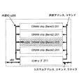
【0026】
図40を参照して、本発明の対象となるメモリサブシステム、即ち、メモリモジュールについて概略的に説明する。まず、図40に示されたメモリモジュールはモジュール基板200、モジュール基板200上に、平面的に並列に配置された複数のDRAMチップ(図では9個)201、モジュール基板200の中央部に配置されたレジスタ202、PLL203、及び、SPD(Serial Presence Detect)204を備え、モジュール基板200は図示しないコネクタによりマザーボード(図示せず)上に取り付けられている。
【0027】
ここで、マザーボード上には、図示されたメモリモジュールのほかに、他のメモリモジュールもチップセット(メモリコントローラ)と共に搭載されており、これら複数のメモリモジュールとチップセットにより、メモリシステムが構成されている。
【0028】
各DRAM201から図の下方に、即ち、モジュール基板200の短辺方向にモジュールデータ配線が施されており、他方、レジスタ202から図の下方にモジュールコマンド・アドレス配線が施されている。更に、PLL203から図の下方にモジュールクロック配線が延びており、これらモジュールコマンド・アドレス配線及びモジュールクロック配線はモジュール基板200の長辺方向に配列されたコネクタに接続されている。また、SPD204はモジュール基板200に搭載されているDRAMチップ201の動作条件を定めるメモリであり、通常、ROMによって構成されている。
【0029】
更に、図示されたレジスタ202からは、モジュール基板200の長辺方向に、即ち、横方向にモジュールコマンド・アドレス分配配線が各DRAMチップ201に対して施されると共に、PLL203からも同様にモジュールクロック分配配線が各DRAMチップ201に施されている。
【0030】
この構成のメモリモジュールでは、メモリアクセスデータバスのバス幅に応じたビット数のデータをモジュールデータとして入出力することができる。しかしながら、この構成では、モジュールデータ配線のトポロジーは、モジュール・コマンド配線からモジュール・コマンド分配配線のトポロジー及びPLL03からのモジュールクロック配線及びモジュールクロック分配配線のトポロジーと相違している。
【0031】
一方、図示されたメモリモジュール構成において、プロセッサーの要求するデータレートを実現するための手段として広いバス幅を持つ方法(DDR等のSDRAMを使った一般のデータ処理システム)と、狭いバス幅で転送速度を上げる(RDRAMのシステム)方法がとられている。
【0032】
これらの方法のうち、広いバス幅で構成された従来の一般的メモリモジュールはIO数が16、8、4の単体DRAMを4〜16個、平面的に並列にモジュール基板上に搭載し、64あるいは72のデータバスを構成している。
【0033】
一方、モジュールコマンド・アドレス信号、モジュールクロック信号は、通常、モジュール基板200上の全てのDRAMチップ201に共用されている。このため、これらの配線は、図示されているように、モジュール基板200上にレジスタ202、PLL203を搭載しておき、これらレジスタ202及びPLL203により、バッファリング、およびモジュール上配線遅延に対するタイミング調整をして、モジュールコマンド・アドレス信号、モジュールクロック信号は各DRAMチップ201に供給されている。
【0034】
前述したように、メモリコントローラ(チップセット)から配信されるデータ信号とアドレスコマンド信号、クロック信号はそれぞれ物理的に異なった配線トポロジーとなっており信号の伝送特性が異なる。
【0035】
この物理的配線トポロジーの差によって各DRAMにおけるデータ信号とモジュールクロック信号およびコマンド・アドレス信号にはPLL203で補整しきれない信号到達時間の差、スキューが生じ、これが転送速度をさらに上げる上で大きな障害になるという問題が生じている。
【0036】
更に、この種のメモリシステムにおける他の問題点としてメモリモジュールの増設を可能にすることに起因するデータ配線上の分岐配線の問題がある。通常、モジュールの増設はバス配線上に接続されたソケットに挿抜することで行われる。このため、データ信号はバス配線上で分岐されてモジュール内DRAMチップ201に与えられる。この分岐配線により生じる信号反射により高速の信号伝送に障害をもたらすという問題が生じている。
【0037】
また、メモリモジュールを増設するほど分岐配線による信号品質の劣化、また、DRAMパッケージに寄生するLCによる信号品質の劣化が増加するためこの構成を用いているDDRIIにおける増設数は2スロットが限界となっているのが実情である。実際、この構成を用いているDDRIIによるメモリサブシステムで実現できるデータレートはデータピンあたり533Mbps1システムチャネルあたり4.26GBps程度である。
【0038】
他方、図示されたような形式のメモリモジュールにおいて、狭いバス幅で転送速度を上げる方法も提案されている(RDRAM)。この方法ではIO数が16の単体RDRAMをバス配線上に直列に接続して配置する。したがって、メモリコントローラから配信されるデータ信号、モジュールアドレス・コマンド信号、及び、モジュールクロック信号はそれぞれ物理的に同じ配線トポロジーとなっており各RDRAMにおける信号到達時間の差、即ち、スキューが生じない。
【0039】
また、各RDRAMはバス上に実装されるため信号配線上に分岐が生じない。
【0040】
したがって、現在、この構成を用いているRDRAMによるメモリサブシステムで実現できているバスの転送速度は、データピンあたり1.066Gbpsとなる。しかしながら、データ幅は2バイトしかないためシステムのデータレートは2.13GBps程度である。更に、メモリシステムのデータレートを上げるため2チャネルのシステムを構成する方法がとられているが、その場合においても、4.26GBps程度である。
【0041】
このRDRAMの構成ではバス上に分岐は生じないが、要求されるメモリ容量を実現するために同一のバス上に4倍以上のRDRAMを接続する必要がある。このように、長いバス上に多数のRDRAMが接続されると、RDRAMパッケージに寄生するLCによる信号品質の劣化が増加する。したがって、メモリ容量の増設数に制限が生じシステムに要求されるメモリ容量を実現するのが困難である。また、長いバスに多数のDRAMを負荷として接続、保持した状態で、さらに高い要求データレートを実現することは困難である。
【0042】
また、RDRAMにおけるIO数を増やすことも考えられるが、RDRAMチップおよびパッケージが増大し、単体RDRAMのコストが増加する。また同一RDRAMでIO数を増やすほどIO単位でアクセス可能なページサイズが小さくなりシステムの要求を満たさなくなる。
【0043】
本発明の目的は、メモリモジュールにおける様々な問題点を解決して、高速で動作を行うことができるメモリシステムを提供することである。
【0044】
本発明の目的は、高速動作を可能にすると共に消費電流を小さくできるDRAMメモリモジュールを提供することである。
【0045】
本発明の目的は、次世代のメモリサブシステムに要求される12.8GBpsのデータレートにも対処できるメモリモジュール及びメモリシステムを提供することである。
【0046】
【課題を解決するための手段】
本発明では、次世代のメモリサブシステムに要求されるデータレート(12.8GBps)を十分なメモリ容量(増設性)を維持しつつ、且つ、消費電流の増加を抑えたメモリモジュールを実現できる。
【0047】
具体的に言えば、本発明の第1の態様によれば、予め定められたデータ幅を有するシステムデータ信号を入出力するシステム入出力端子と、前記システム入出力端子よりも幅広の内部データ信号をそれぞれ送受する複数のメモリチップを備えたメモリモジュールであって、前記システム入出力端子における前記システムデータ信号と前記内部データ信号との間の変換を行う機能を備えたIOチップを有し、前記複数のメモリチップは前記IOチップ上に積層されると共に、前記IOチップに対して前記積層された複数のメモリチップを貫通する貫通電極によって接続されていることを特徴とするメモリモジュールが得られる。
【0048】
この場合、更に、前記IOチップを実装するためのインターポーザ基板を備え、当該インターポーザ基板は前記システム入出力端子を構成する実装用端子を有している。
【0049】
本発明の第2の態様によれば、予め定められたデータ幅を有するシステムデータ信号を入出力すると共に、前記システムデータ信号よりも幅広の内部データ信号を送受する複数のメモリモジュールを含むメモリシステムにおいて、前記複数のメモリモジュールはそれぞれIOチップと、当該IOチップ上に積層された複数のメモリチップとを積層した構成を備えていることを特徴とするメモリシステムが得られる。
【0050】
この場合、複数のメモリモジュールは共通のマザーボード上に平面的に取り付けられても良いし、或いは、複数のメモリモジュールは共通の実装基板上に搭載され、前記実装基板をマザーボード上に取り付けた構成を有していても良い。
【0051】
本発明の第3の態様によれば、予め定められた転送速度でシステムデータ信号の送受を行うと共に、前記転送速度よりも遅い内部処理速度で内部データ信号を送受する複数のメモリチップとを備えたシステムにおいて、前記予め定められた転送速度のデータ信号を送受する端子を備え、前記内部処理速度の内部データ信号と前記転送速度のシステムデータ信号との間の変換を行うIOチップを有し、前記複数のメモリチップは前記IOチップ上に積層されていることを特徴とするシステムが得られる。
【0052】
本発明の他の態様によれば、IOチップと、当該IOチップ上に積層された複数のDRAMと、1チャネルのメモリサブシステムの機能を構成するのに必要なすべてのシステムデータ信号、システムアドレス信号、システム制御信号、システムクロック信号をそれぞれのBGA端子を有するインターポーザ基板を備え、IOチップ上のそれぞれの入出力回路の入出力用パッド及び入力用パッドに結線し、IOチップ上に積層された複数のDRAMチップとIOチップのデータ信号端子、アドレス信号端子、制御信号端子が貫通電極により接合され、チップ間のデータ信号、アドレス信号、制御信号は貫通電極を介して受送信され、電源およびGNDはBGA端子よりIOチップ上のパッドに供給され、貫通電極を介して各DRAMの電源、GND端子に供給される構成を有することを特徴とするDRAMメモリモジュールが得られる。この場合、前記積層されたDRAMチップ上にSPDチップが積層されていも良い。
【0053】
本発明の他の態様によれば、IOチップと、当該IOチップ上に積層された複数のDRAMチップと、1チャネルのメモリサブシステムの機能を構成するのに必要なすべてのシステムデータ信号、システムアドレス信号、システム制御信号、システムクロック信号をそれぞれのBGA端子を有するインターポーザ基板を備え、各DRAMチップはIOチップから送信される制御信号あるいはアドレス信号と照合することにより信号の受信をするための照合信号を生成するカウンター回路を備え、少なくとも2種類の貫通電極形成パターンを異にするDRAMチップを交互に積層した構成を有することを特徴とするDRAMモジュールが得られる。
【0054】
本発明の他の態様によれば、IOチップと、当該IOチップ上に積層された複数のDRAMチップと、1チャネルのメモリサブシステムの機能を構成するのに必要なすべてのシステムデータ信号、システムアドレス信号、システム制御信号、システムクロック信号をそれぞれのBGA端子を有するインターポーザ基板を備え、積層されるDRAMチップは、全て同一パターンを有すると共に、複数のヒューズ素子を備え、前記ヒューズ素子の切断位置によって、積層位置をあらわす照合信号を生成することを特徴とするDRAMモジュールが得られる。
【0055】
本発明の別の態様によれば、予め定められたデータ幅を有するシステムデータ信号を入出力するシステム入出力端子と、前記システム入出力端子よりも幅広の内部データ信号をそれぞれ送受する複数のメモリチップを備えたDRAMモジュールであって、前記システム入出力端子における前記システムデータ信号と前記内部データ信号との間の変換を行う機能を備えたIOチップを有し、前記複数のメモリチップは前記IOチップ上に積層されると共に、前記IOチップに対して前記積層された複数のメモリチップを貫通する貫通電極によって接続され、且つ、積層された各DRAMチップはバンク構成を有し、システムバンク選択信号からIOチップが論理生成したバンク選択信号により選択的に動作することを特徴とするDRAMモジュールが得られる。
【0056】
本発明の更に別の態様によれば、システムデータ信号を入出力するBGA端子を備えたインターポーザ基板と、当該インターポーザ基板上に搭載された2個のIOチップとを有し、各IOチップはそれぞれ1/2のシステムデータ信号BGA端子に接続されており、アドレス、コマンド、クロック等のデータ以外のBGA端子は共有した構成を備え、前記2つのIOチップ上には、複数のDRAMチップが積層されていることを特徴とするDRAMモジュールが得られる。この場合、前記2つのIOチップ上の積層されたDRAMチップは同時にアクセスされる2ランクを構成される。この構成では、データ信号の端子容量を増加させずにメモリ容量の構成自由度の向上、インターポーザ基板上の配線長を短縮でき、これによって、特性を改善できる。
【0057】
また、前記2つのDRAMチップ積層体の一方の最上段には、SPDチップが搭載されていることが望ましい。
【0058】
本発明の更に別の態様によれば、予め定められたデータ幅を有するシステムデータ信号を入出力するシステム入出力端子と、前記システム入出力端子よりも幅広の内部データ信号をそれぞれ送受する複数のメモリチップを備えたメモリモジュールであって、前記システム入出力端子における前記システムデータ信号と前記内部データ信号との間の変換を行う機能を備えたIOチップを有し、前記複数のメモリチップは前記IOチップ上に積層されると共に、前記IOチップに対して前記積層された複数のメモリチップを貫通する貫通電極によって接続され、更に、各DRAMチップの内部には、個別のアレイ制御回路によって制御される複数のバンクが構成されていることを特徴とするDRAMモジュールが得られる。
【0059】
本発明の更に別の態様によれば、予め定められたデータ幅を有するシステムデータ信号を入出力するシステム入出力端子と、前記システム入出力端子よりも幅広の内部データ信号をそれぞれ送受する複数のメモリチップを備えたメモリモジュールであって、前記システム入出力端子における前記システムデータ信号と前記内部データ信号との間の変換を行う機能を備えたIOチップを有し、前記複数のメモリチップは前記IOチップ上に積層されると共に、前記IOチップに対して前記積層された複数のメモリチップを貫通する貫通電極によって接続され、且つ、前記積層された各DRAMチップはテスト専用パッド及び当該テスト専用パッドに接続されたテスト回路を備えていることを特徴とするDRAMモジュールが得られる。
【0060】
この構成では、DRAMチップテスト時にはテストトリガ信号に同期して、前記テスト専用パッドよりテストコマンド、テストアドレス、テストデータ信号が与えられ、前記テスト回路により生成されたテスト用ラッチ信号により、テスト回路によって生成されたアドレス、コマンド、データ信号を受信し、内部動作を開始する。
【0061】
【発明の実施の形態】
図1を参照すると、本発明の第1の実施形態に係るメモリモジュールが示されており、図1に示されたメモリモジュールは図40に示されたメモリモジュールと同様に、メモリデータバス幅として複数のDRAMチップのデータ幅に相当するデータ信号を入出力できる。このように、図40に示されたメモリモジュールを図1に示された積層構造にすることによって、メモリシステム全体として、複数のメモリサブシステムを含み、各メモリサブシステムにおけるデータレートとして、12.8GBpsを有し、増設によってメモリ容量を大きくできると共に実装面積を縮小できるメモリシステムを構成できる。
【0062】
図示されたメモリモジュールはインターポーザ基板210、当該インターポーザ基板210上に搭載されたIOチップ211、及び、当該IOチップ211上に積層された8個のDRAMチップ201とを備えている。ここでは、IOチップ211に隣接した最下層のDRAMチップから上方に第1乃至第8のDRAMチップと呼ぶこともある。ここで言うメモリモジュールとは、チップセット(CPU)の要求するメモリ容量、データレート(データバス幅(64,72,128,144,RDRAMは16)×転送速度)を満足するように複数のDRAM単体により構成されたメモリサブシステムの構成単位を指す。
【0063】
次に、メモリモジュールを構成する各部分について説明すると、各DRAMチップ201は50μm程度の厚さを備え、IOチップ211と各DRAMチップ201とは貫通電極215によって接続され、当該貫通電極215を介して、データ信号がIOチップ211との間で送受される。ここで、貫通電極215は各DRAMチップ201の一方の面から他方の面へ貫通するチップ間接続電極であり、この例では、銅又はアルミニウムによって形成された72x4(=288)の貫通電極が設けられているものとする。
【0064】
更に、インターポーザ基板210はシリコンによって形成され、1チャネルのメモリサブシステムの機能を構成するのに必要な全てのシステムデータ信号、システムアドレス信号、システム制御信号、システムクロック信号のボード上実装ピッチに対応するBGA端子を有し、各信号BGA端子とシリコンチップで形成されるIOチップ上の各信号パッドとを基板配線およびバンプにより結線することを可能にする機能を備えている。
【0065】
また、IOチップ211は1チャネルのメモリサブシステムの機能を構成するのに必要な全てのシステムデータ信号、システムアドレス信号、システム制御信号、システムクロック信号のパッドおよびインターフェイス回路を有している。ここで、1チャネルとは、チップセット(CPU)が処理するデータの単位であり、ここでは、例えば、64又は72ビットであるものとする。
【0066】
概略的に言えば、IOチップ211は、チップセットより入力された信号をDRAMチップ201を動作させるために再構成する機能と、貫通電極215端子からDRAMチップ201に送信する機能、DRAMチップ201からの信号を貫通電極215端子より受信する機能、及び、DRAMチップ201から受信したデータ信号を再構成してシステムデータ信号として送信する機能を有している。
【0067】
図示されたメモリモジュールは、1チャネルのメモリサブシステムの機能を構成するのに必要なすべてのシステムデータ信号、システムアドレス信号、システム制御信号、システムクロック信号それぞれのためのBGA端子を有するインターポーザ基板210を備えている。インターポーザ基板210のBGA端子は、IOチップ211上のそれぞれの入出力回路の入出力用パッド及び入力用パッドに結線され、IOチップ211上に積層された複数のDRAMチップ201とIOチップ211のデータ信号端子、アドレス信号端子、制御信号端子が貫通電極215により接合され、チップ間のデータ信号、アドレス信号、制御信号は貫通電極215を介して受送信される。また、電源およびGNDはインターポーザ基板210のBGA端子よりIOチップ211上のパッドに供給され、貫通電極215を介して各DRAMチップ201の電源、GND端子に供給される構成を有している。
【0068】
ここで、各DRAMチップ201はシステムデータバス数の2n倍(nは1以上の自然数)の書き込み用および読み出し用、或いは、双方向の貫通電極データ信号端子を有している。一方、IOチップ211はシステムデータバス数の2n倍の書き込み用および読み出し用、あるいは双方向の貫通電極データ信号端子を有している。
【0069】
このような構成を備えたDRAMチップ201及びIOチップ211との間では、貫通電極215のデータ端子を介して相互のデータ転送が行われる。
【0070】
この場合、IOチップ211はシリアルパラレル回路を有し、システムデータバスより伝送された連続した端子あたり2nのデータ信号をシリアルパラレル変換して同時にDRAMチップ201に転送する。更に、IOチップ211はパラレルシリアル回路を有し、DRAMチップ201より転送された端子あたり2nのデータをパラレルシリアル変換して連続する2nのデータとしてシステムデータバスに出力する。
【0071】
更に、IOチップ211は64mビットあるいはパリティビットを含む72mビットのシステムデータバスとのインターフェイスを有する(mは1以上の自然数)。
【0072】
各DRAMチップ201のデータ信号端子は貫通電極215を介してIOチップ211のデータ信号端子に接続される。この場合、データ信号線としての貫通電極215はDRAMチップ201により共有される。また、各DRAMチップ201のアドレス信号端子は貫通電極215をアドレス信号線として共有し、IOチップ211のアドレス信号端子に接続される。更に、各DRAMチップ201の制御信号端子は貫通電極215を制御信号線として共有し、IOチップ211の制御信号端子に接続される。
【0073】
尚、この例では、WPP(Wafer Package Process)により再配線した後、IOチップ211上にはバンプが形成されている。
【0074】
更に、メモリモジュールには、図40と同様にSPDが設けられても良い。この場合、SPDはメモリモジュールのメモリ容量、バンク構成、保証動作スピード,その他の情報を製造時に書き込み、チップセットがシステムブート時に、これを参照して制御条件を自動設定するための機能を備えている。SPDチップがDRAMチップ201の積層体上に設けられる場合、SPDチップの入出力信号端子は貫通電極215を介してIOチップ211上のSPD入出力端子パッドに接続される。また、各DRAMチップ201はSPD入出力信号のための、DRAMチップ201では使用されない貫通電極を備えている。
【0075】
ここで、積層体を構成するDRAMチップ201は、貫通電極215形成以外のパターン形成は同一パターンを有している。このように、積層されるDRAMチップ201は、全て同一のパターンが形成されているから、ヒューズ素子を別途設けておき、このヒューズ素子を各DRAMチップ201毎に切断することによりIOチップ211から個々のDRAMチップ201に対する信号を識別することができる。
【0076】
図2を参照して、本発明の第2の実施形態に係るメモリモジュールを説明する。図2に示された各DRAMチップ201はIOチップ211から送信される制御信号あるいはアドレス信号と照合することにより信号の受信をするための照合信号を生成するカウンター回路300を備え、IOチップ211にはチップ識別コード生成回路301が設けられている。
【0077】
更に、図2に示すように、DRAMチップ201a及び201cは同一の貫通電極形成パターン251を備え、一方、DRAM201bはDRAMチップ201a及び201cの貫通電極形成パターン251とは異なる貫通電極形成パターン252を備えている。IOチップ211とDRAMチップ201aの貫通電極形成パターン251とは、貫通電極215aによって接続されており、DRAMチップ201aと201bとは、貫通電極215bにより、更に、DRAMチップ201bと201cとは、貫通電極215aにより相互に接続されている。図示された貫通電極215a及び215bは2本だけを示しているが、2本以上設けられても良い。尚、他の貫通電極215は図を簡略化するために省略されている。
【0078】
具体的に説明すると、DRAMチップ201a上の貫通電極形成パターン251は当該DRAMチップ201a上のカウンター300に対して貫通電極215aからの信号を入力し、カウンター300からの出力を貫通電極215bに出力している。更に、DRAMチップ201bの貫通電極形成パターン252は当該DRAMチップ201b上のカウンター300に対して、DRAMチップ201aからの出力を供給し、DRAMチップ201bのカウンター300からの出力を貫通電極215aを介して上層のDRAMチップ201cの貫通電極形成パターン251に出力している。この構成では、各DRAMチップ201a、201b、201cのカウント値が順次上層のDRAMチップに出力される。
【0079】
このように、図示されたメモリモジュールは互いに異なる貫通電極形成パターン251及び252を備えたDRAMチップ201を交互に積層した構成を備えている。この構成によれば、IOチップ211から出力された複数ビットの信号が最下層のDRAMチップ201aのカウンター300に入力され、そのカウンター300の出力が次層のカウンター300に与えられ、以下、順次最上層のDRAMチップまでインクリメントされた信号が伝達される構成となっている。この構成では、各DRAMチップにおいて異なるカウンター出力値を得ることができ、これによって、各DRAMチップ201はカウンター出力値を用いて照合信号を内部で発生し、各DRAMチップ201に対する制御信号及びアドレス信号を識別することができる。
【0080】
前述した2種類の貫通電極形成パターン251及び252を備えたDRAMチップ201は貫通電極形成時に2種類のマスクパターンによりカウンター300の入出力を入れ替えるだけで、簡単に製造できる。
【0081】
次に、図3を参照すると、図2に示されたメモリモジュールの全体の具体例が示されている。図3では、図2に示されているように、単一のIOチップ211上に8つのDRAMチップ201(DRAM−1〜DRAM−8)が搭載されている。図4には図3に示されたIOチップ211の一部の構成がより具体的に示されており、図5には図3に示されたDRAMチップ201の具体的構成が示され、更に、図6には図5に示されたDRAMチップ201で使用されるDRAMチップ選択回路がより詳細に示されている。
【0082】
図3を参照すると、IOチップ211はインターポーザ基板(図示せず)との間で各種の信号を送受する入出力回路111、入力回路112、内部コントロール回路113、DLL114、及び、カウンタースタート値生成部115とを有し、更に、データコントロール回路、シリアルパラレル変換回路、パラレルシリアル変換回路、アドレスコントロール回路、バンク選択信号生成回路を備えている。図3では、データコントロール回路、シリアルパラレル変換回路、パラレルシリアル変換回路、の組み合わせを参照番号116によって示し、アドレスコントロール回路及びバンク選択信号生成回路の組み合わせを参照番号117によって示している。また、図4では、アドレスコントロール回路及びバンク選択信号生成回路をそれぞれ参照番号117a及び117bによって示している。
【0083】
図3に示すように、IOチップ211には、メモリコントローラとしてのチップセット(図示せず)から、システムクロック信号CK,/CK、システムアドレス信号A0〜Ai、システムバンクアドレス信号BA0〜BA2が/RAS,/CAS,/WE,/CS,ストローブ信号DQS等の制御信号と共に与えられている。更に、チップセットとIOチップ211との間では、データ信号DQ0〜DQ63及びDM0〜DM7が送受されている。図3に示されたデータコントロール回路及びシリアルパラレル/パラレルシリアル変換回路116としては、通常の回路を使用できるから、ここでは、詳述しないが、当該回路116と各DRAMチップ201との間で、内部データ信号IDQ0−255、IDM0−31が送受される。尚、本発明の実施形態では、DLL114はIOチップ211だけに設置されており、各DRAMチップ201には備えられていない。
【0084】
図3に示されたIOチップ211の回路117には、システムアドレス信号a0−Ai、システムバンクアドレス信号BA0−BA2が与えられていると共に、カウンタスタート値生成部115に接続されている。更に、カウンタスタート値生成部115からは、3ビットのカウント信号S0〜S2が最下層のDRAMチップ201(DRAM−1)のカウンター回路に与えられている。
【0085】
図4をも参照すると、図3に示されたIOチップ211の一部が具体的に示されている。
【0086】
図4には、IOチップ211内の内部コントロール回路113、カウンタースタート値生成部115、アドレスコントロール回路117a、及びバンク選択信号生成回路117bが示されている。このうち、内部コントロール回路113は初期化信号REを出力する。この初期化信号REは、通常ハイレベルを取り、一般に、システムで行われるモジュール上のDRAMチップ201を初期化時に、ローレベルのパルス信号である。
【0087】
図3に示されたメモリモジュールでは、図7に示すように、単一のIOチップ211上に4個のDRAMチップ201を積層しても良いし、図8に示すように、単一のIOチップ211上に8個のDRAMチップ201を積層しても良い。図7及び図8のいずれにおいても、斜線で示されているように、積層されたDRAMチップ201のうちの1つのDRAMチップだけが選択される。このように、本発明に係るメモリモジュールでは、IOチップ211に積層されるDRAMチップ201の数を変更できるから、IOチップ211はDRAMチップ201の積層数を判定できることが必要になる。
【0088】
図7及び図8に示された例では、各DRAMチップ201が単一のバンクを構成し、更に、各DRAMチップ201はx256個のデータ端子を備え、他方、IOチップ211はx64のシステムデータ線を備えている。このため、DRAMチップのデータ端子とIOチップ211のシステムデータ線とは4:1の関係になっている。したがって、この構成では、DRAMチップ201の出力動作周波数は1/4に低減され、ウエハ状態での試験も容易である。また、メモリモジュールに対する一回のリードライトアクセスは全て1つのDRAMチップ201に対して行われることになる。
【0089】
図9を参照すると、図7及び図8に示された各DRAMチップ201のバンク構成が示されている。図9に示されたDRAMチップ201は現状の512MbitDDRIIDRAMと同様に、512Mbitの容量を備え、単一のバンク構成を有している。図示されたDRAMチップ201は4つの128Mbitセルアレイに区分されており、その中央部分に内部接続用領域及びテストパッドが配置されている。当該DRAMチップのアドレスが指定されると、各セルアレイ領域において2つの領域が活性化され、各アレイから64ビット、合計256ビットのデータ信号の読出、書込が可能になる。ここで、活性化状態とは、センスアンプが動作可能になる状態を意味し、この状態におけるデータ単位をページと呼ぶ。この結果、図示されたDRAMチップ201は8kバイトのページを有していることになる。
【0090】
図7〜図9に示された構成を前提として、図3〜6に示されたメモリモジュールの動作を説明する。図4に示されたIOチップ211のアドレスコントロール回路117aには、図3からも明らかな通り、システムアドレス信号A0−Aiのほかに、システムのバンクアドレス信号BA0−BA2が与えられている。
【0091】
この状態で、図4に示されたアドレスコントロール回路117aはバンクアドレス信号BA0−BA2から目的のDRAMチップ201のバンク、ここでは、積層位置を判定して、バンク選択信号生成回路117bに出力する。
【0092】
バンク選択信号生成部117bには、積層数認識信号線C8R,C4Rを介して積層数認識信号が与えられている。
【0093】
この例では、図8のように、DRAMチップ201を8層積層した場合、積層数認識信号線C8R,C4Rはともにハイとなり、この結果、IOチップ211のバンク選択信号生成部117bから生成されるバンク選択信号BA0N/T〜BA2N/Tは全てイネーブルとなり、メモリモジュールはシステムのバンクアドレス信号BA0,1,2を取り込んで8バンク構成で動作する。
【0094】
他方、図7のように、DRAMチップ201を4層積層した場合、積層数認識信号線C8Rがロー,C4Rがハイとなり、IOチップ211のバンク選択信号生成部117bから生成されるバンク選択信号BA0N/T〜BA1N/Tがイネーブルとなり、BA2N/Tはハイレベルに固定される。この結果、メモリモジュールはシステムのバンクアドレス信号BA0,1を取り込んで4バンク構成として動作する。
【0095】
図4に示された内部コントロール回路113は、通常ハイレベルで、モジュール上のDRAMチップ201の初期化時にローレベルのパルス信号となる初期化信号REを生成する。この初期化信号REは積層数認識信号線(C4R,C8R)にそれぞれ接続された積層数認識信号線上のレベルを初期化する。初期化信号REによって初期化されると、積層数認識信号線(C4R,C8R)の状態は前述したように、積層されるDRAMチップ201の数に応じたレベルになる。
【0096】
また、図4のカウンタスタート値生成部115は3ビットのカウント信号S0−S2を出力する。この例では、カウント信号S0−S2は111であるものとする。この結果、最下層のDRAMチップ201のカウンター回路300では、1だけインクリメントし、その出力として、000を出力する。以下、各層のDRAMチップ201のカウンター回路300では同様に1だけインクリメントしたカウント値を順次上層に送出する。
【0097】
その結果、DRAMチップ201を積層した場合、下層から4番目のDRAMチップ201からの出力により、積層数認識信号線C4Rがハイとなり、下層から8番目のDRAMチップ201は積層されていないため、積層数認識信号線C8Rはローのままとなる。DRAMチップ201を8層積層した場合は、下層から4番目のDRAMチップ201からの出力により積層数認識信号線C4Rがハイとなると共に、下層から8番目のDRAMチップ201からの出力により積層数認識信号線C8Rがハイとなる。これにより、DRAMチップ201の積層数が認識できる。
【0098】
次に、図5に示されたDRAMチップ201はIOチップ211のカウンタースタート値生成部115に接続されたカウンター回路300を含むDRAMチップ選択回路ブロック150を備えている。図示されたDRAMチップ201はカラムデコーダ、センスアンプ、データアンプ、ロウデコーダ等を含むメモリセルアレイ170のほかにコントロール回路171、アドレスバッファ172、及び、データバッファ173を備えている。
【0099】
更に、図示されたDRAMチップ201は積層される関係で各DRAMチップ201毎にテストをすることができないことを考慮して、DRAMチップ201上にテスト用パッド175及びテスト回路176を搭載していることをも特徴としている。
【0100】
ここで、図6をも参照すると、DRAMチップ選択回路ブロック150のカウンター回路300には前述したカウント信号S0−S2がカウント入力信号S0_in〜S2_inとして与えられ、1だけインクリメントしたカウント値を上層のDRAMチップ201にカウンター出力S0_out〜S2_outとして送出する。
【0101】
更に、図示されたカウンター回路300はカウンター出力S0_out〜S2_outに応じて照合信号(S0T/N〜S2T/N)を生成し、DRAM内ラッチ信号生成回路151に出力する。DRAM内ラッチ信号生成回路151は、カウンター回路300から与えられる照合信号(S0T/N〜S2T/N)をIOチップ211のバンク選択信号生成回路117bから送信されるバンク選択信号(BA0T/N〜BA2T/N)と照合し、一致した場合にDRAMチップ内でDRAM内ラッチ信号を生成する。尚、図示されたDRAM内ラッチ信号生成回路151には、図3に示されているように、IOチップ211内の内部コントロール回路113からラッチ信号LATも与えられている。
【0102】
DRAM内ラッチ信号が図5のコントロール回路171、アドレスバッファ172、及び、データバッファ173に与えられ、メモリセルアレイ170から256ビットのデータ信号を読出し、或いは、メモリセルアレイ170に対して書込み可能な状態になる。
【0103】
尚、図6に示されたカウンター回路300は4層構造及び8層構造の際に、それぞれ最上層に位置するDRAMチップ201を識別するために、位置制御信号C4及びC8が論理回路を介してC4R、C8Rに出力されている。
【0104】
この構成を備えた各DRAMチップ201は、DRAMチップ選択回路ブロック150の動作により、IOチップ211で論理生成されたバンク選択信号(BA0T/N〜BA2T/N)を受けて、選択的に動作することになる。
【0105】
更に、図5に示すように、DRAM内ラッチ信号はDRAMチップ内のコントロール回路171に入力し、コマンド信号に応じてDRAMチップ201のコントロール信号を生成し、アドレスバッファ172、データバッファ173に入力し、IOチップ211から送信されたデータ信号をDRAMチップ201内に取り込むことができる。
【0106】
また、積層数認識信号線C4R、C8Rのレベルにより積層されたDRAMチップ数を認識し、各DRAMチップに対して制御信号或いはアドレス信号の論理レベルの割り振りを行っていることが判る。
【0107】
更に、図示されたテスト回路176はコントロール回路171、アドレスバッファ172、及び、データバッファ173に接続されており、これらの回路171及びバッファ172、173に対してテスト用ラッチ信号を出力すると共に、テストコマンド信号、テストアドレス信号、及び、テストデータ信号をも出力する。これによって、積層されたDRAMチップ201を個別にテストすることができる。
【0108】
図10を参照すると、図6に示されたDRAMチップ選択回路ブロック150内のカウンター入力信号S0_in〜S2_in、出力信号S0−out〜S2_out、照合信号(S0T/N〜S2T/N)、及び、位置制御信号C4及びC8の値が最下層の第1層から第8層まで順に示されている。
【0109】
図6に示されたDRAMチップ201では、その選択回路ブロック150内にカウンター回路300を設け、このカウンター回路300により、DRAMチップ201における照合信号(S0T/N〜S2T/N)を生成している。このように、カウンター回路300を用いた構成では、図2を参照して説明したように、互いに異なる貫通電極形成パターン251、252をDRAMチップ201に形成する必要がある。
【0110】
図11に示されたDRAMチップ選択回路ブロック150aは積層されるDRAMチップ201全てのパターンを同じにして、積層されたDRAMチップ201の積層位置に応じた照合信号(S0T/N〜S2T/N)を生成できる構成を備えている。具体的に言えば、図示されたDRAMチップ選択回路ブロック150aはカウンター回路300(図6)の代わりに、初期化信号REを受けて動作するヒューズ回路180を有している。ここでは、8層のDRAMチップ201を積層する場合を考慮して、3つのヒューズ回路180が設けられている。
【0111】
図からも明らかな通り、各ヒューズ回路180はNチャンネルMOSとPチャンネルMOSとのドレイン間にヒューズ素子181を設けると共に、当該ヒューズ素子181の一端に一対のインバータ回路を設けた構成を備え、一対のインバータ回路の両端の出力がDRAM内ラッチ信号生成回路151に与えられている。このヒューズ素子181をDRAMチップ201の積層位置に応じて、切断することによって、図6と同様に照合信号を生成することができる。
【0112】
この構成によれば、DRAMチップ201のパターンは層毎に変える必要はなくなるが、ヒューズ素子181の切断個所の異なるDRAMチップ201を積層数に応じて製造する必要がある。
【0113】
尚、図示されたDRAMチップ201は照合信号に応じて、貫通電極を介して各DRAMチップ201とIOチップ211で共有する積層数認識信号線(C4R,C8R)のレベルを変化させ、これによって、最上層のDRAMチップを識別することができる。
【0114】
図12〜14を参照して、本発明に係るDRAMチップの選択方法の他の例を説明する。図12に示されたメモリモジュールは1個のIOチップ211と8個のDRAMチップ201を備え、内部コントロール回路113から各DRAMチップ201に対応したチップセレクト信号CSEL1〜8が8本の貫通電極端子を通して、各DRAMチップ201に出力されている点で、図3に示されたメモリモジュールとは相違している。このため、アドレスコントロール回路117aには、システムアドレス信号A0〜Ai及びシステムのバンクアドレス信号BA0〜2に与えられており、バンク選択信号生成回路117b(図3)が設けられていない点で、図3のメモリモジュールとは相違している。
【0115】
図13に示されたIOチップ211のアドレスコントロール回路117aはシステムのバンクアドレス信号BA0〜2から内部バンクアドレス信号を生成し、内部コントロール回路113aに出力する。内部コントロール回路113aは内部バンクアドレス信号から、積層されたDRAMチップ201の積層位置に応じたチップ選択信号CSEL1〜8を生成する。当該チップ選択信号CSEL1〜8は8本の貫通電極端子のいずれか1本を選択し、当該1本の貫通電極端子に出力される。カウンタースタート値生成部115及び積層数認識信号線C4R、C8Rについては図4で説明したから、ここでは、詳述しない。
【0116】
図14を参照すると、図13から出力されるチップ選択信号CSEL1〜8及びカウント信号S0〜S2を受けて動作するDRAMチップ選択回路ブロック150が示されている。図14に示されたDRAM選択回路ブロック150はカウント信号S0〜S2をカウント入力信号S0_in〜S2_inとして受け、カウンター出力信号S0_out〜S2_outを出力すると共に、DRAMチップ201の積層数に応じた本数の出力端子B1〜B8を備えている。
【0117】
この例では、カウンター回路300は、カウンター値に応じて、出力端子b1〜8の1本を選択して、DRAMチップ内ラッチ信号生成回路151に出力する。この場合、出力端子B1〜B8はDRAMチップ201の層番目だけがハイレベルとなり、その他はローレベルとなる。
【0118】
図示されたDRAMチップ内ラッチ信号生成回路151には、貫通電極を介して、いずれか1つがハイレベルを取るチップ選択信号CSEL1〜8が与えられている。このため、積層位置(層番目)のDRAMチップ211のDRAM内ラッチ信号生成回路151からDRAM内ラッチ信号が出力され、選択された貫通電極からの信号のみがDRAMチップ201に取り込まれる。
【0119】
ここでは、チップ選択信号CSELによりDRAM内ラッチ信号が生成され、前述した方法と同様に動作する例を示したが、本方式の方法はIOチップ211と個々のDRAMチップ201との信号の受送信を行う手段とすることができる。
【0120】
図14ではカウンター回路300を用いて、積層位置を識別し、DRAM内ラッチ信号を出力するDRAMチップ選択回路ブロック150について説明したが、カウンター回路300の代わりに、図11と同様にヒューズ回路180を各チップ選択信号CSEL1〜8に対応して設けても良い。
【0121】
図15を参照すると、図14の変形例として、ヒューズ回路180をDRAMチップ201の積層数に応じた数だけ設けた例が示されている。図示されたDRAMチップ選択回路ブロック150bは、初期化信号RE端子に接続された8個のヒューズ回路180を備え、ヒューズ回路180の出力端子はそれぞれチップ選択信号CSEL1〜8に対応して設けられたNANDゲートに接続されている。ヒューズ回路180の構成自体は図11と同様であるから説明を省略するが、各ヒューズ回路180のヒューズ素子181を切断することによりB1〜B8に対応した信号を生成することができる。
【0122】
図16を参照すると、本発明の第3の実施形態に係るメモリモジュールが示されており、当該メモリモジュールは、従来の2ランクメモリモジュールと同等のメモリ容量を有することができる。図示されたメモリモジュールは2つのDRAMチップ201を同時にアクセスの対象とする場合に適した構成を示している。
【0123】
具体的に言えば、メモリモジュールはインターポーザ基板(図示せず)上に搭載された2つのIOチップ211a及び211bと、IOチップ211a、211b上にそれぞれ4層のDRAMチップ201a、201bを積層し、各IOチップ211a、211b上のDRAMチップ201a、201bが1つづつ同時にアクセスされ、2ランクのメモリモジュールを構成している。この場合、同時にアクセスされたDRAMチップ201a、201bとIOチップ211a、211bとの間では、それぞれx256ビットのデータ信号が送受され、各IOチップ211a、211bとチップセットとの間では、x32ビットのシステムデータ信号が送受される。図では、同時にアクセスの対象となる一対のDRAMチップ201a、201bはそれぞれ同一バンク0〜3を構成している。
【0124】
一方、システムアドレス信号、コマンド、及び、クロック信号は2つのIOチップ211a、211b共通に与えられている。更に、各IOチップ211a、211bはインターポーザ基板上のシステムデータ信号BGA端子の半分にそれぞれ接続され、データ信号以外の信号端子は両IOチップ211a、211bで共有する構成を採用している。このように、インターポーザ基板上のシステムデータ信号BGA端子の半分に、IOチップ211a、211bを接続することにより、入力容量の増加による信号の伝送特性の劣化を軽減できる。
【0125】
図17を参照すると、図16に示されたメモリモジュールの変形例として、2つのIOチップ211a、211b上に8個のDRAMチップ201a、201bを積層したメモリモジュールが示されており、この関係で、各IOチップ211a、211bには、最下層の第1層から最上層の第8層まで、バンク0〜7のDRAMチップ201a、201bがそれぞれ積層されている。
【0126】
この例においても、2個のIOチップ211a、11bはそれぞれインターポーザ基板上の1/2のシステムデータ信号BGA端子に接続され、アドレス、コマンド、クロック等のデータ以外のBGA端子は共有している。
【0127】
このように、インターポーザ基板上に2個のIOチップ211a、211bを搭載することでデータ信号のインターポーザ基板上のBGA端子からIOチップ211a、211b上のパッドまでの配線長を短縮させることができることが確認された。
【0128】
図16及び17に示された例では、DRAMチップ201a、201bはx256のデータ端子を有し、IOチップ211a、211bのパラレルシリアル変換回路でシステムのx32のデータ線に対して入出力されているから、DRAMチップ201a、201bのデータ端子とシステムのデータ線とは8:1の構成になっており、より高い動作周波数に対応できる。
【0129】
上記した実施形態のほかに、各DRAMチップ201を2バンク構成とすることも可能である。
【0130】
図18を参照すると、512MbitのDRAMチップ201を256MbitのバンクAとバンクBとの2バンク構成にした例が示されている。このように、2バンク構成にした場合、DRAMチップ201内部は半分だけ活性化され、活性化されたバンクAからは256ビットのデータ信号が読出し可能な状態となる。また、各DRAMチップ201を2バンク構成にすると、活性化されるページサイズは図9の場合に比較して半分となり、図18では4kバイトのページサイズとなる。
【0131】
図19を参照すると、本発明の第4の実施形態に係るメモリモジュールは2バンク構成のDRAMチップを積層した構成を備えている。図示された例では、インターポーザ基板210(図示せず)上に2個のIOチップ211a、211bを搭載し、2つのIOチップ211a、211b上にそれぞれ2つのDRAMチップ201a、201bを積層した構成を有している。各IOチップ211a、211bに積層されたDRAMチップ201a,201bはそれぞれ図19に示されているように2バンク構成を有している。
【0132】
図示されたDRAMチップ201a、201bのうち、IOチップ211a,211bに最も近接した、即ち、最下層のDRAMチップ201a,201bにはバンク0、2が割り当てられており、他方、上層のDRAMチップ201a,201bにはバンク1、3が割り当てられている。
【0133】
ここで、各IOチップ211a,211bはそれぞれ1/2のシステムデータ信号BGA端子に接続し、アドレス、コマンド、クロック等のデータ以外のBGA端子を共有している。
【0134】
この構成によれば、データ信号の端子容量を増加させずにメモリ容量の構成自由度を向上させることが出来ると共に、インターポーザ基板上の配線長短縮による特性を改善できる。
【0135】
図20を参照すると、図19に示されたメモリモジュールの変形例として、2つのIOチップ211a,211b上に、2バンク構成の4つのDRAMチップ201a,201bをそれぞれ積層した例が示されている。この場合、4つのDRAMチップ201a,201bには最下層から最上層まで、バンク(0,4),(1,5),(2,6),(3,7)が割り当てられ、各バンクとIOチップ211a,211bとの間では、x128のデータ信号が送受され、他方、各IOチップ211a,211bとチップセットとの間では、x32のシステムデータ信号が送受される。
【0136】
図21を参照すると、図19に示されたメモリモジュールの他の変形例が示されている。図からも明らかな通り、2つのIOチップ211a,211b上に、2バンク構成のDRAMチップ201a,201bが8個積層されている点以外、図19及び20と同様である。
【0137】
図19〜21に示されたように、各DRAMチップ201a,201bを複数のバンク構成にした場合、全体で、DRAMチップ数x(DRAMチップ内のバンク数)に等しいバンク数を有するメモリモジュールを構成することができる。この場合、DRAMチップ201a,201bの内部を複数(n個)のバンクとして動作させるときのページサイズは1/nとなる。また、BGA端子レベルによりDRAMチップ201a,201bの内部を複数(n個)のバンクとして動作させるかどうかを選択するように構成することも可能である。
【0138】
図22〜図24を参照して、図19〜図21に示されたメモリモジュールの具体的な回路構成について説明する。図22に示された各IOチップ211には、2バンク構成の各DRAMチップ201a,201bを制御するコントロール信号MIO、MBが与えられ、当該コントロール信号MIO、MBはIOチップ211の内部コントロール回路113に供給されている。ここで、コントロール信号MBはメモリモジュール内の複数のDRAMチップ201a、201bを2バンク構成にするか否かを指示するバンクモード信号であり、コントロール信号MIOはIOチップ211a、211bを選択する信号である。
【0139】
内部コントロール回路113aはこのようなコントロール信号MIO、MBを受けて動作し、アドレスコントロール回路、バンク選択信号制御回路117を制御する。図示された内部コントロール回路113aはコマンド信号及びラッチ信号LATを生成する点では図3に示された内部コントロール回路113と同様である。また、アドレスコントロール回路、バンク選択信号制御回路117は後述するようにバンク選択信号BSELT/Nを生成する。
【0140】
図23を参照して、図22に示されたIOチップ211を具体的に説明すると、システムバンクアドレス信号BA0〜BA3を受けて動作するアドレスデータコントロール回路117aは内部バンク選択信号(BA0T/NP〜BA3T/NP)を個別にバンク選択信号生成回路117bに出力している。
【0141】
一方、内部コントロール回路113は、バンクモードMBを受けて、DRAMチップ210のバンク構成を設定する内部バンクモード信号MBSを出力し、更に、IOチップ211a、211bの構成を設定するコントロール信号MIOSをも出力する。尚、内部バンクモード信号MBSはDRAM内部を2バンク構成にするかしないかを決定する信号である。このことは、図示されたメモリモジュールは2バンク、或いは、単一のバンクで選択的に動作させることができることを意味している。
【0142】
図23に示されたバンク選択信号生成回路117bは、内部バンク選択信号(BA0T/NP〜BA3T/NP)及び積層数認識線(C4R、C8R)上の信号を論理演算して、当該IOチップ211a又は211b上におけるバンクを選択するバンク選択信号(BA0T/N〜BA2T/N)を出力する一方、各DRAMチップ201a,201b内のバンク構成を指定するバンク構成選択信号BSELT、BSELNをも出力する。
【0143】
図24を参照すると、図23に示されたIOチップ211a,211b上に積層された各DRAMチップ201(添字省略)はメモリセルアレイ1(バンクA)とメモリセルアレイ2(バンクB)とを有し、これらバンクA,Bはバンクモード信号MBSに応じて、単一のバンク或いは2バンク構成で選択的に動作する。
【0144】
具体的に説明すると、図24に示されたDRAMチップ201はカウンター回路300を備えたDRAMチップ選択回路ブロック150を有し、更に、コントロール回路171、アドレスバッファ172、データバッファ173、テスト回路176、及び、テスト用パッド176を有している。ここで、DRAMチップ選択回路ブロック150及びテスト回路176は前述した実施形態において既に説明したから、ここでは説明を省略する。
【0145】
図示されたコントロール回路171は内部バンクモード信号MBS及びコントロール信号MIOSを受けて、当該MBS及びMIOSに応じて、メモリセルアレイ1及び2にコントロール信号1及び2を出力する。更に、各DRAMチップ201a,201b内のバンクレベルを指定するバンクレベル選択信号BSELT、BSELNはアドレスバッファ172に与えられる。アドレスバッファ172は当該BSELT、BSELNにしたがってメモリセルアレイ1及び2にカラムアドレス信号を出力すると共に、ロウアドレス信号1、2をメモリセルアレイA,Bに出力する。
【0146】
このことからも明らかなとおり、図24に示されたコントロール回路171、アドレスバッファ172、及び、データバッファ173はメモリアレイを制御するアレイ制御回路として動作する。
【0147】
この動作以外の動作は前述した実施形態と同様であるので、説明を省略する。
【0148】
図23に示したIOチップ211では、システムのバンクモード信号MBに応じて、内部コントロール回路113では、バンクモード信号MBSを生成している。
【0149】
図25には、IOチップ211の別の例が示されている。図示されたIOチップ211の内部コントロール回路113には、インターポーザ基板上のBGA端子からDRAMチップ積層数識別信号MC8及びMC4が与えられている。この内部コントロール回路113はシステムのバンクモード信号MBだけでなく、当該MC8及びMC4で指定されたレベルをも参照して、バンクモード信号MBSを生成している。
【0150】
上記した実施形態では、DRAM内部を2バンク構成にするかしないかをBGA端子MBに与えられる信号で制御されるようにした。このため、システムのマスターの要求に応じて内部バンク構成を可変にすることができる。MB端子には、システムにより固定電位を与えてもよいし、システムコマンド信号と同じに切り替えることも可能である。
【0151】
前述したように、DRAMチップ内を2バンクの構成にした場合、DRAMの積層数を2層でも最小のDRAM容量に対応できる。更に、4層、8層の構成を同じIOチップ、DRAMチップで構成することができ、種々のメモリ容量要求に対応でき生産性が向上する。
【0152】
バンク数を多くすることによる効果について説明しておくと、システムによってはメモリバンクの使用方法が異なっているが、ページヒット率が高い場合、バンクを活性化した状態でシステムからの要求を待つのでページ長が長い方がヒット率の向上に効果がある。また、ページヒット率が低い場合には、バンクを閉じた状態でシステムからの要求を待つのでバンク数が多いほうが望ましい。
【0153】
ここで、メモリモジュールには、モジュールのメモリ容量、バンク構成、保証動作スピード,その他の情報を製造時に書き込み、チップセットがシステムブート時に、これを参照して制御条件を自動設定するための機能を有するSPDチップが搭載されている場合がある。このようなSPDチップを備えたメモリモジュールにも本発明は同様に適用できる。
【0154】
図26を参照すると、本発明の第4の実施形態に係るメモリモジュールがしめされている。図示されたメモリモジュールはインターポーザ基板210上に一つのIO基板即ちIOチップ211を搭載し、当該IO基板211上に8層からなるDRAMチップ201を積層している。更に、最上層のDRAMチップ201上にSPDチップ400が搭載されている。当該SPDチップ400は前述したようにメモリ容量等を書き込んだROMであり、システムブート時、チップセットから当該SPDチップ400の制御条件が読み出され、その条件が自動的にシステム内に設定される。
【0155】
SPDチップ400はDRAMチップ201と同様に、貫通電極215によりIOチップ211に接続され、更に、IOチップ211上のパッドを介してインターポーザ基板210に接続されている。
【0156】
図示されたメモリモジュールの動作はブート時の動作以外、第2の実施形態に係るメモリモジュールと同様である。
【0157】
図27を参照すると、SPDチップ400を使用した別の例が示されている。ここでは、インターポーザ基板210上に、2つのIOチップ211a,211bが搭載されている。IOチップ211a,211bにはそれぞれ8層のDRAMチップ201a,201bが積層されている。更に、図示された例では、SPDチップ400はIOチップ211a上のDRAMチップ201aにだけ取り付けられている。SPDチップ400は貫通電極215を介してIOチップ211aに接続されている。
【0158】
この構成では、貫通電極215を介してSPD信号をIOチップ201aで読み取ることができる。
【0159】
チップセットはシステムブート時にSPDチップ400に書き込まれた情報を読み出す。この情報をIOチップ211a、211b内に取り込み、DRAMチップ201a,201bのコントロール信号(MBS;DRAMチップ内のバンク構成、MIOS;DRAMチップのIO構成)を生成する。
【0160】
このように、メモリモジュールの初期設定時に、IOチップ201a,201bがSPDチップ400に読み出しアクセスをかけることで、SPDチップ400に製造時に書き込まれた内部タイミング設定、モジュール構成等の設定情報を読み取り内部回路の設定を行うことも可能になる。
【0161】
また、図27に示すように、2個のIOチップ211a,211bを搭載する場合、片側のDRAMチップ201a上にのみ、SPDチップ400を搭載し、貫通電極215でIOチップ211a上のパッドに結線し、更に、インターポーザ基板210上配線により、もう一方のIOチップ211bのパッドに結線される。これによって、両方のIOチップ211a,211bでSPDチップ400からの信号を読み取ることが可能となる。
【0162】
図28を参照すると、図27に示されたメモリモジュールの積層構造が示されている。図からも明らかな通り、SPDチップ400は左側のDRAMチップ201a上だけに配置されており、右側のDRAMチップ201b上には配置されていない。更に、図示された各DRAMチップ201a,201bは2バンク構成を有し、この関係で、各DRAMチップ201a,201bには2つのバンクレベルが与えられている。
【0163】
システムアドレス、コマンド、クロック信号は2つのIOチップ211a,211bに共通に与えられると共に、システムブート時には、SPDチップ400がアクセスされる。SPDチップ400はアクセスされると、SPD信号(SCL,SDA,SA0−SA2)をIOチップ211a,211b及びチップセットに出力する。
【0164】
図29には、図28に示されたIOチップ211a、DRAMチップ201a、SPDチップ400の接続関係が示されており、図30には、IOチップ211bとDRAMチップ201bとの接続関係が示されている。図示されたIOチップ211aはSPDチップ400に接続されたSPDコード解読回路500を備え、当該SPDコード解読回路500においてSPD信号を解読して、解読結果を内部コントロール回路113に出力している。内部コントロール回路113では、解読結果に応じてIO内調整信号を入出力回路111及び入力回路112に供給して、初期設定を行なうと共に、コントロール信号MBS及びMIOSを当該IOチップ211a上のDRAMチップ201aに供給して各DRAMチップ201aを初期設定する。
【0165】
SPD信号は当該IOチップ201aを介して、図30に示されたIOチップ211bのSPDコード解読回路500にも供給され、解読結果は当該IOチップ211b内の内部コントロール回路113に与えられ、IOチップ211a上のDRAMチップ201aの場合と同様に、DRAMチップ201bの初期設定を行なう。
【0166】
図31を参照して、上記した本発明に係るメモリモジュールの動作を説明する。尚、メモリモジュールの動作は全ての実施形態において基本的には同様である。IOチップ211はシステムコマンド信号(ACT,RED,PRE)をチップセットから受信すると、DRAMチップ201に対してラッチ信号LAT及びアドレス信号IA0〜IAi、バンク選択信号BA0−2T/N、コマンド信号、内部データ信号(x256)を送信する。
【0167】
図示された例では、システムクロック信号として400MHzが与えられ、システムクロック信号に同期して、システムコマンド(ACT,RED,PRE)が与えられ、システムコマンドACT,REDに応じてラッチ信号LAT信号及びDRAM内ラッチ信号が所定のタイミング後、出力される。図からも明らかな通り、ラッチ信号LATとDRAM内ラッチ信号とは同じ時間間隔で生成されている。
【0168】
DRAMチップ201はIOチップ211より送信されるラッチ信号LATによりアドレス、コマンド、データ信号を受信し内部動作を開始する。ここで、コマンド信号はシステムクロックに同期したラッチ信号LATによってDRAMチップ201に送信されるのでメモリモジュール内コマンド信号間のタイミングはシステム上の時間間隔と同じになる。
【0169】
図示されているように、システムコマンドACTがアドレス信号ADDと共に与えられると、対応するDRAMチップが活性化され、この状態で読出コマンドREDが与えられると、256ビットの内部データが64ビット単位で4回、システムデータとして読み出される。
【0170】
図32を参照すると、システムコマンドとして、連続的に読出コマンドREDがシステムアドレスAddと共に与えられた場合の動作が示されており、この場合にも、tRAS期間中に、256ビットの内部データが64ビット単位のシステムデータとして連続的に読み出されている。
【0171】
他方、図33には、システムコマンドACT後、書込コマンド(WRT)が与えられた場合の動作が示されている。この場合、システムコマンドACT及びWRTに同期して、DRAMチップ内では、DRAM内ラッチ信号、コマンド信号、内部アドレス信号が生成され、64ビット単位のシステムデータ信号がDRAMラッチ信号に同期して、256ビットの内部データ信号として書き込まれる。
【0172】
本発明に係るメモリモジュール内のDRAMチップ201には、前述したように、テスト用パッド175及びテスト回路176が内蔵されている。
【0173】
図34を参照して、各DRAMチップ201をテストした場合における書込み動作を説明する。この場合、DRAMチップ201には、テストコマンド信号(ACT,RED,PRE)がテストパッド175からテストトリガ信号に同期して与えられる。テストコマンド信号を受信すると、テスト回路176はテスト用ラッチ信号、テストアドレス、テストコマンド、テストデータ信号をアドレスバッファ172、コントロール回路171、データバッファ173に送信する。図示された例では、テストパッド数を削減するためテスト用信号はテスト用トリガ信号の立ち上がり、立下りに連続して入力され、テスト回路176でモジュレートされテストアドレス、テストコマンドとして生成される。
【0174】
テストデータ信号は1ピンから入力され、内部のx256IOは縮退されてテストされる。DRAMチップ201はテスト回路176より送信されるテスト用ラッチ信号によりアドレス、コマンド、データ信号を受信し内部動作を開始する。
【0175】
ここで、テストコマンドはテストトリガ信号に同期したテスト用ラッチ信号によって内部動作信号とされるので、DRAMチップ内コマンド間のタイミングはテストコマンドのタイミング間隔と同じになる。
【0176】
図35は各DRAMチップ201の読出動作をテストする場合の動作を示すタイミングチャートである。読出動作時には、期待値データがテストデータ入出力から入力され、内部読み出しデータと比較され、比較結果がラッチされる。
【0177】
判定結果は図36に示す比較サイクルで出力され、リセットされる。
【0178】
図36に判定結果をラッチするDRAMチップ内信号ラッチ回路の構成が示されている。図37に示されたラッチ回路は、テストの際に使用され、テスト用ラッチ信号によってテストアドレス、コマンド、データ信号をラッチする回路部分と、通常動作時に使用され、DRAM内ラッチ信号によってアドレス、コマンド、データ信号をラッチする回路部分とは共通の出力部を備えている。この構成では、ラッチする回路部における信号のDRAMチップ内生成タイミング間隔がテスト時と実装時で同一にできるのでウエハ状態でのDRAMチップの不良除去が可能となる。
【0179】
図38を参照して、上記した本発明に係るメモリモジュールを使用して構成されたメモリシステムについて説明する。図示されたメモリシステムは、図1等に示されたDRAMチップ201の積層体を含むメモリモジュール(400a〜400dで示す)をマザーボード401上にメモリコントローラ(チップセット)402と共に搭載されている。
【0180】
図示された例において、各メモリモジュール400a〜400dはマザーボード401に平面的に実装されている。この関係で、マザーボード401には、メモリモジュール400a〜400dの実装位置に平面実装ソケット403が設けられており、メモリモジュール400a〜400dはそれぞれ平面実装ソケット403のパッドに対し、インターポーザ基板210のBGA端子により電気的に接続されている。
【0181】
この場合、各メモリモジュール400a〜400dに設けられたインターポーザ基板210のBGA端子には、メモリシステムのデータ信号、アドレスコマンド信号、クロック信号、及び、制御信号が与えられる。これらの信号は各メモリモジュール400a〜400dのIOチップ211上のそれぞれの信号パッド、更に、インターフェイス回路に供給される。各メモリモジュール400a〜400d内の結線は極めて短いため、信号配線上においては、電気的に無視できる(@1.6Gbps)ほどの分岐しか生じない。
【0182】
図示された例では、データ信号、アドレスコマンド信号、及び、クロック信号の配線はそれぞれ物理的に同じ配線トポロジーとすることができる。このため、各メモリモジュール400a〜400d(特に、IOチップ入力パッド)における信号到達時間の差(即ち、スキュー)が生じない。
【0183】
この構成では、チャネルあたりのバス幅はDDRIIモジュールと同等以上にできるため、バスに接続されるパッケージ数はRDRAMのように増加しないと言う利点がある。
【0184】
次に、図39に示されたメモリシステムは、図38に示されたメモリモジュール400a〜400dを平面実装ソケット403を介して実装基板410に実装し、当該実装基板410をスロット及びコネクタ(図示せず)により、マザーボード401上に搭載した構成を有している。このように、本発明のメモリシステムはマザーボード401上に、積層メモリモジュール400a〜400dを搭載した実装基板410を立設するような構成を摂っても良い。この図に示された構成においても、データ信号(DQ)、アドレスコマンド信号、及び、クロック信号の配線は実質上、互いに物理的に同じ配線トポロジーとすることができる。このため、各メモリモジュール400a〜400d(特に、IOチップ入力パッド)におけるスキューを抑制できる。
【0185】
図39に示された実装基板410を2つのスロットに実装したメモリシステムについて1.6Gbpsでライト、リードのシミュレーションを行ったところ、アイパターンに充分なウィンドウが開くことが確認された。また、同様に、4スロットにおいても充分なウィンドウが得られた。
【0186】
他方、2スロットに16個のデバイスが実装されたRDRAMについて、同様なシミュレーションを行ったところ、充分なウィンドウが得られなかった。
【0187】
これは、16デバイスがバスに接続された場合、遠端デバイスでの受信波形は他のデバイス入力LCによる反射信号の影響を受けるためであると考えられる。
【0188】
上記した実施形態では、DRAMチップについてのみ説明したが、本発明は何等これに限定されることなく、外部データ信号の転送速度及び幅がモジュール内の内部データ信号の転送速度及び幅と異なるシステムに適用できる。
【0189】
【発明の効果】
前述したように、本発明に係るDRAMメモリモジュールはインターポーザ、IOチップ、貫通電極、及び、複数のDRAMチップを積層した構造を有している。この構造によれば、アドレス,コマンド,クロック信号の入力回路はIOチップ上にのみ搭載されるため、従来のメモリモジュール上で各DRAMチップが消費していたアドレス,コマンド,クロック信号の入力回路の消費電流はIOチップ上の1セット分のみとなる。同様に、従来各DRAMチップに搭載されていたDLLは本発明のメモリモジュールでは、IOチップ上にのみ搭載され、消費電流は1セット分のみとなる。本発明の構造では、モジュール基板上配線は貫通電極に相当し、貫通電極は50μm程度で8層の積層でも450μmほどで配線の充放電電流は極めて小さい。このため、本発明では、従来のモジュールでの基板上配線充放電電流を大幅に削減できる。
【0190】
本発明に係るメモリモジュールでは、メモリコントローラからの1つのアクセス命令に対してモジュール内の1つのDRAMチップのみがアクセスされる。従来のDDRモジュールの場合のようにモジュール上の全てのDRAMチップ或いは1/2のDRAMチップにアクセスする場合におけるDRAMチップ上のコントロール回路部およびコントロール信号の重複動作をなくすことでモジュール全体の動作電流を削減できる。
【0191】
更に、本発明に係るメモリモジュールでは、従来DDR等のシステムでモジュール上配線遅延に対するタイミング調整のために搭載されているレジスター、PLLは必要ないため、これらの能動部品による消費電流が削減される。
【0192】
また、DDRIIシステムで必要とされるDRAMチップ内のデータ信号配線(DQ)のターミネーションは必要としないため、ここで消費されるDC電流が削減できる。
【0193】
本発明のメモリモジュールでは、動作電流を削減するためメモリコントローラからの1つのアクセス命令に対してモジュール内の1つのDRAMチップのみがアクセスされる。
【0194】
また、積層されるDRAMチップは生産性を考慮して貫通電極を含むすべてのパターンが共通のものが望ましい。このように、全てのパターンを共通にした場合、IOチップから個別のDRAMチップに信号を送信して動作させることは困難になると言う問題が生じる。しかしながら、この問題は、各DRAMチップにIOチップから送信される制御信号あるいはアドレス信号と照合することにより信号の受信をするための照合信号を生成するカウンター回路を設けることによって解決される。このようなカウンター回路に対する配線は、貫通電極を形成した後、DRAMチップのパターンを形成が終了したウエハに対して行われる。
【図面の簡単な説明】
【図1】本発明に係るメモリモジュールの概略構成を示す図である。
【図2】本発明の実施形態に係るメモリモジュールの構成を示す分解図である。
【図3】図2に示されたメモリモジュールの全体構成を示すブロック図である。
【図4】図3に示されたIOチップ211の一部の構成をより具体的に示すブロック図である。
【図5】図3に示されたDRAMチップ201の具体的構成を示すブロック図である。
【図6】図5に示されたDRAMチップ201で使用されるDRAMチップ選択回路をより詳細に示すブロック図である。
【図7】本発明に係るメモリモジュールの一例をそのアクセス方法と共に説明するための図である。
【図8】本発明に係るメモリモジュールの他の例をそのアクセス方法と共に説明するための図である。
【図9】図7及び図8に示されたDRAMチップの活性化状態を示す図である。
【図10】図6に示された信号関係を示す図である。
【図11】図5に示されたDRAMチップ201で使用されるDRAMチップ選択回路の他の構成例を示すブロック図である。
【図12】本発明に係るDRAMチップの選択方法の他の例を説明するブロック図である。
【図13】図12に示されたIOチップの構成を具体的に説明するブロック図である。
【図14】図12に示されたDRAMチップの具体的構成を示すブロック図である。
【図15】図12に示されたDRAMチップの変形例を示すブロック図である。
【図16】本発明の他の実施形態に係るDRAMモジュールの概略構成及びそのアクセス方法を説明するブロック図である。
【図17】本発明の他の実施形態に係るDRAMモジュールの変形例及びそのアクセス方法を説明するブロック図である。
【図18】本発明の更に他の実施形態に係るDRAMモジュールにおける各DRAMチップの構成を説明する図である。
【図19】図18に示されたDRAMモジュールの構成例を示す図である。
【図20】図18に示されたDRAMモジュールの他の構成例を示す図である。
【図21】図18に示されたDRAMモジュールの更に他の構成例を示す図である。
【図22】図18〜図21に示されたDRAMモジュールにおける動作を説明するためのブロック図である。
【図23】図22に示されたIOチップの構成を具体的に説明するブロック図である。
【図24】図22に示されたDRAMチップの構成を具体的に説明するブロック図である。
【図25】図22に示されたIOチップの他の構成例を示すブロック図である。
【図26】本発明の別の実施形態に係るDRAMモジュールの概略構成を示す図である。
【図27】本発明の更に他の実施形態に係るDRAMモジュールの概略構成を示す図である。
【図28】図27に示されたDRAMモジュールのバンク及び配線を説明する図である。
【図29】図28に示されたDRAMモジュールにおけるDRAM積層体の一方の構成を説明するブロック図である。
【図30】図28に示されたDRAMモジュールの他方のDRAM積層体の構成を説明するブロック図である。
【図31】本発明に係るDRAMモジュールにおける読出動作を説明するタイムチャートである。
【図32】本発明に係るDRAMモジュールにおいて連続読出動作が行われる場合を説明するタイムチャートである。
【図33】本発明に係るDRAMモジュールにおける書込動作を説明するタイムチャートである。
【図34】本発明に係るDRAMモジュールにおけるテストデータの書込動作を説明するタイムチャートである。
【図35】本発明に係るDRAMモジュールにおけるテストデータ読出動作を説明するタイムチャートである。
【図36】本発明に係るDRAMモジュールにおけるテストデータ比較動作を説明するタイムチャートである。
【図37】テストの際使用されるデータラッチ回路を説明する回路図である。
【図38】本発明に係るDRAMモジュールを複数個含むメモリシステムの一例を説明する斜視図である。
【図39】本発明に係るDRAMモジュールを複数個含むメモリシステムの他の例を説明する斜視図である。
【図40】従来のDRAMモジュールを説明する平面図である。
【符号の説明】
201、201a、201b、201c DRAMチップ
210 インターポーザ基板
211 IOチップ
215、215a、215b 貫通電極[0001]
BACKGROUND OF THE INVENTION
The present invention relates to a memory system including a plurality of memory modules as memory subsystems, and more particularly to a memory system including a plurality of memory units in each memory module.
[0002]
[Prior art]
Conventionally, this type of memory system has a configuration in which a plurality of memory modules are mounted on a motherboard, and these memory modules are controlled by a chipset (memory controller). Each memory module has a plurality of DRAMs as memory units. There is a DRAM memory system installed.
[0003]
The above-mentioned DRAM memory system employs SSTL (Stub Series Terminated Transceiver Logic) as an interface standard, and uses a DDR (Double Data Rate) system that inputs and outputs data in synchronization with the leading and trailing edges of the clock. Thus, a system capable of writing and reading data at high speed with low signal amplitude has been proposed.
[0004]
As an example of such a memory system, Japanese Patent Laid-Open No. 2001-256772 (hereinafter referred to as Patent Document 1) discloses a memory in which a plurality of memory modules (that is, DRAM modules) mounted with a plurality of DRAMs are mounted on a motherboard. A system is disclosed. Specifically, the memory module includes a rectangular memory module substrate, a plurality of DRAMs arranged in parallel in the longitudinal direction of the memory module substrate, a command / address buffer arranged between the DRAMs, and And a PLL chip that distributes the clock to each DRAM, and each memory module constitutes a memory subsystem.
[0005]
Here, each DRAM on the memory module is connected to a module data line extending in the short side direction of the module substrate, and the command / address buffer and the PLL chip are respectively a module command / address line and a module extending in the short side direction of the module substrate. Connected to clock wiring.
[0006]
Further, in order to distribute command addresses and clocks from the command address buffer and PLL chip to each DRAM, module command address distribution lines and module clock distribution lines are drawn out in the long side direction of the module substrate. .
[0007]
In this configuration, the data signal is directly given from the memory controller provided on the motherboard board to the DRAM chip on the memory module constituting each memory subsystem, and the command / address signal and the clock signal are supplied to the memory controller. To the DRAM chip on each memory module via a command / address buffer and a PLL chip.
[0008]
According to this memory module configuration, the system data signal can be transferred to the external circuit at a high speed even if the writing and reading speed for the DRAM chip is slower than the transfer speed of the system data signal.
[0009]
However, as shown in
[0010]
On the other hand, in Japanese Patent Laid-Open No. 6-291250 (Patent Document 2), a plurality of IC chips each having a signal pad are laminated at a position where the vertical and horizontal dimensions are standardized and the standards are standardized. A semiconductor integrated circuit configured to be connected by vertical wiring is disclosed.
[0011]
In
[0012]
In
[0013]
Further, in Japanese Patent Laid-Open No. 9-504654 (Patent Document 3), a single IC chip is replaced with an IC chip laminated body, and an interface circuit for translating signals between the host system and the IC chip laminated body is provided. A memory package contained in a body is disclosed (claim 2). Also in this example, the stacked IC chip stacks are selectively controlled by the interface circuit so as to operate independently. In this case, the width and transfer speed of the data signal between the host system and the IC chip stack are the same as the width and transfer speed of the internal data signal in the IC chip stack.
[0014]
In other words, the cited document 3 does not take into consideration the case where the internal data width inside the IC chip stack is wider than the data signal width outside the IC chip stack.
[0015]
US Pat. No. 6,133,640 (Patent Document 4) also discloses a memory having a three-dimensional structure. In this patent document 4, the memory circuit and the control logic circuit are individually arranged on a plurality of physically separated layers, and the memory circuit of each layer is individually optimized by a single control logic circuit. Discloses a configuration for operating a plurality of memory circuits to reduce costs.
[0016]
[Patent Document 1]
JP 2001-256772 A
[0017]
[Patent Document 2]
JP-A-6-291250
[0018]
[Patent Document 3]
JP-T 9-504654
[0019]
[Patent Document 4]
US Pat. No. 6,133,640
[0020]
[Problems to be solved by the invention]
Among the above-mentioned
[0021]
In the memory system disclosed in
[0022]
However, in such a memory subsystem, when the number of DRAMs mounted on the module substrate increases, it is not possible to meet the demand for higher speeds, particularly the demand for a high data rate of 12.8 Gbps in the next generation memory module. There was found.
[0023]
As a result of diligent research on the cause that hinders the speed increase in the above-described DRAM module, the present inventors have found that data between the memory controller and each DRAM chip is not obtained when a plurality of DRAM chips are arranged in a plane on the mounting substrate. Since the wiring topology of the signal, address command signal, and clock signal differs by several centimeters on the mounting substrate, the difference in signal arrival time, that is, skew occurs due to this difference in wiring topology. It has been found that if the transfer speed is increased, correction cannot be performed even if a PLL is used.
[0024]
Furthermore, when the transfer speed is increased, there is a problem that the current consumption in the memory subsystem increases accordingly. Each DRAM chip on the memory module is equipped with a DLL circuit for receiving and transmitting a high-frequency transmission signal, and the current consumption is about 15% of the Read / Write current at 800 Mbps. The increase is inevitable.
[0025]
Hereinafter, the above-described problem will be described in detail with reference to FIG.
[0026]
With reference to FIG. 40, a memory subsystem, ie, a memory module, which is an object of the present invention will be schematically described. First, the memory module shown in FIG. 40 is arranged on the
[0027]
Here, in addition to the illustrated memory modules, other memory modules are also mounted on the motherboard together with a chip set (memory controller). A memory system is configured by the plurality of memory modules and the chip sets. Yes.
[0028]
Module data wiring is provided from each
[0029]
Further, from the illustrated
[0030]
In the memory module having this configuration, data of the number of bits corresponding to the bus width of the memory access data bus can be input / output as module data. However, in this configuration, the topology of the module data wiring is different from the topology of the module command wiring to the module / command distribution wiring and the topology of the module clock wiring and the module clock distribution wiring from the PLL 03.
[0031]
On the other hand, in the illustrated memory module configuration, a method having a wide bus width (a general data processing system using SDRAM such as DDR) as a means for realizing the data rate required by the processor, and transfer with a narrow bus width. The method of increasing the speed (RDRAM system) is taken.
[0032]
Among these methods, a conventional general memory module configured with a wide bus width includes 4 to 16 single DRAMs with 16, 8, and 4 IOs mounted on a module substrate in parallel in a plane. Alternatively, 72 data buses are configured.
[0033]
On the other hand, the module command / address signal and the module clock signal are usually shared by all the DRAM chips 201 on the
[0034]
As described above, the data signal, the address command signal, and the clock signal distributed from the memory controller (chip set) have physically different wiring topologies and have different signal transmission characteristics.
[0035]
Due to the difference in physical wiring topology, the data signal, module clock signal, and command / address signal in each DRAM have a difference in signal arrival time and a skew that cannot be compensated by the
[0036]
Furthermore, another problem in this type of memory system is a problem of branch wiring on the data wiring caused by enabling the addition of memory modules. Usually, modules are added and removed by inserting and removing from sockets connected on the bus wiring. Therefore, the data signal is branched on the bus wiring and supplied to the in-
[0037]
Further, as the number of memory modules is increased, the signal quality deteriorates due to the branch wiring, and the signal quality deteriorates due to the LC parasitic on the DRAM package. Therefore, the number of expansions in the DDRII using this configuration is limited to two slots. It is the actual situation. In fact, the data rate that can be realized by a memory subsystem based on DDRII using this configuration is about 4.26 Gbps per data pin per 533 Mbps per system channel.
[0038]
On the other hand, a method of increasing the transfer speed with a narrow bus width in a memory module of the type shown in the figure has been proposed (RDRAM). In this method, a single RDRAM having 16 I / Os is arranged in series on the bus wiring. Therefore, the data signal, the module address / command signal, and the module clock signal distributed from the memory controller have physically the same wiring topology, and there is no difference in signal arrival time in each RDRAM, that is, no skew.
[0039]
Further, since each RDRAM is mounted on the bus, no branching occurs on the signal wiring.
[0040]
Therefore, the bus transfer rate currently realized by the memory subsystem using the RDRAM using this configuration is 1.066 Gbps per data pin. However, since the data width is only 2 bytes, the data rate of the system is about 2.13 Gbps. Furthermore, in order to increase the data rate of the memory system, a method of configuring a two-channel system is used, but in that case, it is about 4.26 Gbps.
[0041]
In this RDRAM configuration, no branching occurs on the bus, but in order to realize the required memory capacity, it is necessary to connect four or more times more RDRAMs on the same bus. As described above, when a large number of RDRAMs are connected on a long bus, signal quality deterioration due to LC parasitic on the RDRAM package increases. Therefore, the number of additional memory capacities is limited and it is difficult to realize the memory capacity required for the system. Further, it is difficult to achieve a higher required data rate in a state where a large number of DRAMs are connected and held as loads to a long bus.
[0042]
Although it is conceivable to increase the number of IOs in the RDRAM, the number of RDRAM chips and packages increases, and the cost of a single RDRAM increases. Further, as the number of IOs in the same RDRAM is increased, the page size accessible in IO units is reduced, and the system requirement is not satisfied.
[0043]
An object of the present invention is to provide a memory system capable of solving various problems in a memory module and operating at high speed.
[0044]
An object of the present invention is to provide a DRAM memory module that enables high-speed operation and can reduce current consumption.
[0045]
An object of the present invention is to provide a memory module and a memory system that can cope with a data rate of 12.8 Gbps required for a next-generation memory subsystem.
[0046]
[Means for Solving the Problems]
According to the present invention, it is possible to realize a memory module that maintains a sufficient memory capacity (expandability) at a data rate (12.8 Gbps) required for a next-generation memory subsystem and suppresses an increase in current consumption.
[0047]
Specifically, according to the first aspect of the present invention, a system input / output terminal for inputting / outputting a system data signal having a predetermined data width, and an internal data signal wider than the system input / output terminal. A memory module including a plurality of memory chips that respectively transmit and receive, and an IO chip having a function of performing conversion between the system data signal and the internal data signal at the system input / output terminal, A plurality of memory chips are stacked on the IO chip, and a memory module is obtained in which the memory chip is connected to the IO chip by a through electrode penetrating the plurality of stacked memory chips.
[0048]
In this case, an interposer substrate for mounting the IO chip is further provided, and the interposer substrate has a mounting terminal constituting the system input / output terminal.
[0049]
According to the second aspect of the present invention, a memory system including a plurality of memory modules for inputting / outputting a system data signal having a predetermined data width and transmitting / receiving an internal data signal wider than the system data signal. The memory system is characterized in that each of the plurality of memory modules has a configuration in which an IO chip and a plurality of memory chips stacked on the IO chip are stacked.
[0050]
In this case, the plurality of memory modules may be planarly mounted on a common motherboard, or the plurality of memory modules are mounted on a common mounting board, and the mounting board is mounted on the motherboard. You may have.
[0051]
According to a third aspect of the present invention, there is provided a plurality of memory chips that transmit and receive system data signals at a predetermined transfer rate, and transmit and receive internal data signals at an internal processing rate slower than the transfer rate. The system has a terminal for transmitting and receiving the data signal of the predetermined transfer rate, and has an IO chip for converting between the internal data signal of the internal processing rate and the system data signal of the transfer rate, A system is obtained in which the plurality of memory chips are stacked on the IO chip.
[0052]
According to another aspect of the present invention, an IO chip, a plurality of DRAMs stacked on the IO chip, and all system data signals and system addresses necessary for configuring the functions of a one-channel memory subsystem. Signals, system control signals, and system clock signals are provided with interposer boards having respective BGA terminals, and connected to input / output pads and input pads of respective input / output circuits on the IO chip, and stacked on the IO chip. Data signals terminals, address signal terminals, and control signal terminals of a plurality of DRAM chips and IO chips are joined by through electrodes, and data signals, address signals, and control signals between the chips are transmitted and received through the through electrodes, and the power supply and GND Is supplied from the BGA terminal to the pad on the IO chip, and the power source of each DRAM, G DRAM memory module characterized by having a structure that is supplied to the D terminal is obtained. In this case, an SPD chip may be stacked on the stacked DRAM chip.
[0053]
According to another aspect of the present invention, an IO chip, a plurality of DRAM chips stacked on the IO chip, and all system data signals and systems necessary for configuring the function of a one-channel memory subsystem The interposer board having the BGA terminals for address signals, system control signals, and system clock signals is provided, and each DRAM chip is collated for receiving signals by collating with control signals or address signals transmitted from the IO chip. A DRAM module having a counter circuit for generating a signal and having at least two types of DRAM chips having different through electrode formation patterns stacked alternately is obtained.
[0054]
According to another aspect of the present invention, an IO chip, a plurality of DRAM chips stacked on the IO chip, and all system data signals and systems necessary for configuring the function of a one-channel memory subsystem The address signal, the system control signal, and the system clock signal are each provided with an interposer substrate having respective BGA terminals, and the stacked DRAM chips all have the same pattern and have a plurality of fuse elements, depending on the cutting positions of the fuse elements. A DRAM module characterized by generating a verification signal representing the stacking position can be obtained.
[0055]
According to another aspect of the present invention, a system input / output terminal for inputting / outputting a system data signal having a predetermined data width, and a plurality of memories for transmitting / receiving internal data signals wider than the system input / output terminal, respectively. A DRAM module including a chip, the IO chip having a function of performing conversion between the system data signal and the internal data signal at the system input / output terminal; Stacked on the chip, connected to the IO chip by a through electrode penetrating the plurality of stacked memory chips, and each stacked DRAM chip has a bank configuration, and a system bank selection signal The DRAM module is characterized in that the IO chip selectively operates according to a bank selection signal generated by logic. Le is obtained.
[0056]
According to still another aspect of the present invention, an interposer substrate having a BGA terminal for inputting / outputting system data signals and two IO chips mounted on the interposer substrate are provided. It is connected to a 1/2 system data signal BGA terminal, and has a shared configuration for BGA terminals other than data such as address, command, clock, etc., and a plurality of DRAM chips are stacked on the two IO chips. A DRAM module can be obtained. In this case, the stacked DRAM chips on the two IO chips constitute two ranks that are accessed simultaneously. With this configuration, it is possible to improve the degree of freedom in configuring the memory capacity and shorten the wiring length on the interposer substrate without increasing the terminal capacity of the data signal, thereby improving the characteristics.
[0057]
In addition, it is desirable that an SPD chip is mounted on the top of one of the two DRAM chip stacks.
[0058]
According to still another aspect of the present invention, a system input / output terminal that inputs and outputs a system data signal having a predetermined data width, and a plurality of internal data signals that are wider than the system input / output terminal, respectively. A memory module including a memory chip, the IO chip having a function of converting between the system data signal and the internal data signal at the system input / output terminal; Stacked on the IO chip and connected to the IO chip by a through electrode penetrating the plurality of stacked memory chips, and each DRAM chip is controlled by an individual array control circuit. A DRAM module characterized in that a plurality of banks are configured can be obtained.
[0059]
According to still another aspect of the present invention, a system input / output terminal that inputs and outputs a system data signal having a predetermined data width, and a plurality of internal data signals that are wider than the system input / output terminal, respectively. A memory module including a memory chip, the IO chip having a function of converting between the system data signal and the internal data signal at the system input / output terminal; Stacked on the IO chip and connected to the IO chip by a through electrode penetrating the plurality of stacked memory chips, and each of the stacked DRAM chips has a test dedicated pad and the test dedicated pad. A DRAM module characterized by comprising a test circuit connected to the circuit is obtained.
[0060]
In this configuration, a test command, a test address, and a test data signal are given from the test-dedicated pad in synchronization with a test trigger signal during a DRAM chip test, and a test latch signal generated by the test circuit is used by a test circuit. The generated address, command, and data signals are received, and internal operations are started.
[0061]
DETAILED DESCRIPTION OF THE INVENTION
Referring to FIG. 1, a memory module according to a first embodiment of the present invention is shown. The memory module shown in FIG. 1 has the same memory data bus width as the memory module shown in FIG. Data signals corresponding to the data widths of a plurality of DRAM chips can be input / output. As described above, the memory module shown in FIG. 40 has the stacked structure shown in FIG. 1, so that the entire memory system includes a plurality of memory subsystems, and the data rate in each memory subsystem is 12. It is possible to configure a memory system having 8 Gbps and capable of increasing the memory capacity and reducing the mounting area by expansion.
[0062]
The illustrated memory module includes an interposer substrate 210, an
[0063]
Next, each part constituting the memory module will be described. Each
[0064]
In addition, the interposer substrate 210 is made of silicon and supports all on-board mounting pitches of system data signals, system address signals, system control signals, and system clock signals necessary to configure the functions of a one-channel memory subsystem. And has a function of enabling connection between each signal BGA terminal and each signal pad on the IO chip formed of a silicon chip by substrate wiring and bumps.
[0065]
The
[0066]
Generally speaking, the
[0067]
The illustrated memory module includes an interposer substrate 210 having BGA terminals for all system data signals, system address signals, system control signals, and system clock signals necessary to configure the functions of the one-channel memory subsystem. It has. The BGA terminal of the interposer substrate 210 is connected to the input / output pads and input pads of the respective input / output circuits on the
[0068]
Here, each
[0069]
Mutual data transfer is performed between the
[0070]
In this case, the
[0071]
Further, the
[0072]
The data signal terminal of each
[0073]
In this example, bumps are formed on the
[0074]
Further, the SPD may be provided in the memory module as in FIG. In this case, the SPD has a function for writing the memory capacity, bank configuration, guaranteed operation speed, and other information of the memory module at the time of manufacture, and automatically setting the control conditions by referring to this when the chipset is booted. Yes. When the SPD chip is provided on the stacked body of the
[0075]
Here, the
[0076]
A memory module according to a second embodiment of the present invention will be described with reference to FIG. Each
[0077]
Further, as shown in FIG. 2, the
[0078]
More specifically, the through electrode formation pattern 251 on the
[0079]
Thus, the illustrated memory module has a configuration in which
[0080]
The
[0081]
Next, referring to FIG. 3, a specific example of the entire memory module shown in FIG. 2 is shown. In FIG. 3, as shown in FIG. 2, eight DRAM chips 201 (DRAM-1 to DRAM-8) are mounted on a
[0082]
Referring to FIG. 3, the
[0083]
As shown in FIG. 3, the
[0084]
The
[0085]
Referring also to FIG. 4, a part of the
[0086]
FIG. 4 shows an
[0087]
In the memory module shown in FIG. 3, four
[0088]
In the example shown in FIGS. 7 and 8, each
[0089]
Referring to FIG. 9, the bank configuration of each
[0090]
The operation of the memory module shown in FIGS. 3 to 6 will be described on the premise of the configuration shown in FIGS. As apparent from FIG. 3, the
[0091]
In this state, the
[0092]
The bank selection
[0093]
In this example, as shown in FIG. 8, when eight layers of
[0094]
On the other hand, as shown in FIG. 7, when four layers of
[0095]
The
[0096]
Further, the counter start
[0097]
As a result, when the
[0098]
Next, the
[0099]
Further, considering that the illustrated
[0100]
Here, referring also to FIG. 6, the
[0101]
Further, the illustrated
[0102]
A latch signal in the DRAM is supplied to the
[0103]
In the
[0104]
Each
[0105]
Further, as shown in FIG. 5, the latch signal in the DRAM is input to the
[0106]
Further, it can be seen that the number of stacked DRAM chips is recognized based on the level of the stacked number recognition signal lines C4R and C8R, and the logical level of the control signal or address signal is assigned to each DRAM chip.
[0107]
Further, the illustrated
[0108]
Referring to FIG. 10, counter input signals S0_in to S2_in, output signals S0-out to S2_out, verification signals (S0T / N to S2T / N), and positions in the DRAM chip selection circuit block 150 shown in FIG. The values of the control signals C4 and C8 are shown in order from the lowest layer, the first layer to the eighth layer.
[0109]
In the
[0110]
The DRAM chip
[0111]
As is apparent from the figure, each
[0112]
According to this configuration, it is not necessary to change the pattern of the
[0113]
The illustrated
[0114]
With reference to FIGS. 12 to 14, another example of the DRAM chip selection method according to the present invention will be described. The memory module shown in FIG. 12 includes one
[0115]
The
[0116]
Referring to FIG. 14, there is shown a DRAM chip selection circuit block 150 which operates in response to the chip selection signals CSEL1 to 8 and count signals S0 to S2 output from FIG. The DRAM selection circuit block 150 shown in FIG. 14 receives the count signals S0 to S2 as the count input signals S0_in to S2_in, outputs the counter output signals S0_out to S2_out, and outputs a number corresponding to the number of stacked
[0117]
In this example, the
[0118]
The DRAM chip latch
[0119]
Here, an example in which a latch signal in the DRAM is generated by the chip selection signal CSEL and operates in the same manner as described above is shown. However, in this method, signal transmission / reception between the
[0120]
In FIG. 14, the DRAM chip selection circuit block 150 that uses the
[0121]
Referring to FIG. 15, as a modification of FIG. 14, an example is shown in which fuse
[0122]
Referring to FIG. 16, a memory module according to a third embodiment of the present invention is shown, and the memory module can have a memory capacity equivalent to that of a conventional two-rank memory module. The illustrated memory module has a configuration suitable when two
[0123]
Specifically, the memory module includes two
[0124]
On the other hand, the system address signal, command, and clock signal are provided in common to the two
[0125]
Referring to FIG. 17, as a modification of the memory module shown in FIG. 16, there is shown a memory module in which eight
[0126]
Also in this example, the two
[0127]
In this way, by mounting the two
[0128]
In the example shown in FIGS. 16 and 17, the
[0129]
In addition to the above-described embodiment, each
[0130]
Referring to FIG. 18, there is shown an example in which a 512
[0131]
Referring to FIG. 19, the memory module according to the fourth embodiment of the present invention has a configuration in which two-bank configuration DRAM chips are stacked. In the illustrated example, two
[0132]
Of the
[0133]
Here, each of the
[0134]
According to this configuration, the degree of freedom in configuring the memory capacity can be improved without increasing the terminal capacity of the data signal, and the characteristics due to the shortening of the wiring length on the interposer substrate can be improved.
[0135]
Referring to FIG. 20, as a modification of the memory module shown in FIG. 19, there is shown an example in which four
[0136]
Referring to FIG. 21, another modification of the memory module shown in FIG. 19 is shown. As is apparent from the figure, this is the same as FIGS. 19 and 20 except that eight
[0137]
As shown in FIGS. 19 to 21, when each
[0138]
A specific circuit configuration of the memory module shown in FIGS. 19 to 21 will be described with reference to FIGS. Each
[0139]
The
[0140]
Referring to FIG. 23,
[0141]
On the other hand, the
[0142]
The bank selection
[0143]
Referring to FIG. 24, each DRAM chip 201 (subscript omitted) stacked on the
[0144]
Specifically, the
[0145]
The illustrated
[0146]
As is clear from this, the
[0147]
Since operations other than this operation are the same as those in the above-described embodiment, description thereof will be omitted.
[0148]
In the
[0149]
FIG. 25 shows another example of the
[0150]
In the above-described embodiment, whether or not the DRAM has a two-bank configuration is controlled by a signal applied to the BGA terminal MB. For this reason, the internal bank configuration can be made variable according to the request of the system master. The MB terminal may be given a fixed potential by the system, or can be switched to the same as the system command signal.
[0151]
As described above, when the DRAM chip has a two-bank configuration, the minimum DRAM capacity can be accommodated even if the number of stacked DRAMs is two. Furthermore, the configuration of 4 layers and 8 layers can be configured by the same IO chip and DRAM chip, and it is possible to meet various memory capacity requirements and improve productivity.
[0152]
To explain the effect of increasing the number of banks, the usage of memory banks varies depending on the system, but if the page hit rate is high, it waits for a request from the system with the bank activated. The longer the page length, the more effective the hit rate. Further, when the page hit rate is low, it is desirable that the number of banks is large because a request from the system is waited with the banks closed.
[0153]
Here, the memory module has a function for automatically setting the control conditions by referring to the memory capacity of the module, the bank configuration, the guaranteed operation speed, and other information written at the time of manufacture. There is a case where an SPD chip is mounted. The present invention can be similarly applied to a memory module having such an SPD chip.
[0154]
Referring to FIG. 26, a memory module according to a fourth embodiment of the present invention is shown. In the illustrated memory module, one IO substrate, that is, an
[0155]
Similar to the
[0156]
The operation of the illustrated memory module is the same as that of the memory module according to the second embodiment except for the operation at the time of booting.
[0157]
Referring to FIG. 27, another example using the
[0158]
In this configuration, the SPD signal can be read by the
[0159]
The chip set reads information written in the
[0160]
As described above, when the memory modules are initially set, the
[0161]
As shown in FIG. 27, two
[0162]
Referring to FIG. 28, a stacked structure of the memory module shown in FIG. 27 is shown. As is apparent from the figure, the
[0163]
The system address, command, and clock signal are commonly supplied to the two
[0164]
29 shows the connection relationship between the
[0165]
The SPD signal is also supplied to the SPD
[0166]
The operation of the memory module according to the present invention will be described with reference to FIG. The operation of the memory module is basically the same in all the embodiments. When receiving a system command signal (ACT, RED, PRE) from the chip set, the
[0167]
In the illustrated example, 400 MHz is given as the system clock signal, system commands (ACT, RED, PRE) are given in synchronization with the system clock signal, and the latch signal LAT signal and DRAM are given in accordance with the system commands ACT, RED. The internal latch signal is output after a predetermined timing. As is apparent from the figure, the latch signal LAT and the in-DRAM latch signal are generated at the same time interval.
[0168]
The
[0169]
As shown in the figure, when system command ACT is applied together with address signal ADD, the corresponding DRAM chip is activated, and when read command RED is applied in this state, 256-bit internal data is converted into 4 bits in units of 64 bits. Times as system data.
[0170]
Referring to FIG. 32, there is shown an operation in the case where a read command RED is continuously given as a system command together with a system address Add. In this case as well, the 256-bit internal data is 64 bits during the tRAS period. It is continuously read as system data in bit units.
[0171]
On the other hand, FIG. 33 shows an operation when a write command (WRT) is given after the system command ACT. In this case, in the DRAM chip, a DRAM latch signal, a command signal, and an internal address signal are generated in synchronization with the system commands ACT and WRT, and a 64-bit system data signal is synchronized with the DRAM latch signal to 256. Written as a bit internal data signal.
[0172]
The
[0173]
Referring to FIG. 34, the write operation when each
[0174]
The test data signal is input from
[0175]
Here, since the test command is used as an internal operation signal by the test latch signal synchronized with the test trigger signal, the timing between the commands in the DRAM chip is the same as the timing interval of the test command.
[0176]
FIG. 35 is a timing chart showing the operation when the read operation of each
[0177]
The determination result is output and reset in the comparison cycle shown in FIG.
[0178]
FIG. 36 shows the configuration of a signal latch circuit in the DRAM chip that latches the determination result. The latch circuit shown in FIG. 37 is used at the time of a test, and a circuit portion that latches a test address, a command, and a data signal by a test latch signal, and is used during a normal operation, and an address and a command by a latch signal in the DRAM. The circuit portion for latching the data signal has an output portion in common. In this configuration, since the generation timing interval of signals in the DRAM chip in the circuit unit to be latched can be made the same during the test and during the mounting, it is possible to remove the defective DRAM chip in the wafer state.
[0179]
With reference to FIG. 38, a memory system configured using the memory module according to the present invention will be described. In the illustrated memory system, a memory module (indicated by 400 a to 400 d) including a stacked body of
[0180]
In the illustrated example, the
[0181]
In this case, a data signal, an address command signal, a clock signal, and a control signal of the memory system are given to the BGA terminal of the interposer substrate 210 provided in each of the
[0182]
In the illustrated example, the wiring of the data signal, the address command signal, and the clock signal can be physically the same wiring topology. For this reason, the difference (namely, skew) of the signal arrival time in each
[0183]
In this configuration, the bus width per channel can be equal to or greater than that of the DDRII module, and thus there is an advantage that the number of packages connected to the bus does not increase as in RDRAM.
[0184]
Next, in the memory system shown in FIG. 39, the
[0185]
When a memory system in which the mounting
[0186]
On the other hand, when a similar simulation was performed for an RDRAM in which 16 devices were mounted in 2 slots, a sufficient window could not be obtained.
[0187]
This is considered to be because when 16 devices are connected to the bus, the received waveform at the far-end device is affected by the reflected signal from the other device input LC.
[0188]
In the above embodiment, only the DRAM chip has been described. However, the present invention is not limited to this, and the transfer rate and width of the external data signal are different from those of the internal data signal in the module. Applicable.
[0189]
【The invention's effect】
As described above, the DRAM memory module according to the present invention has a structure in which an interposer, an IO chip, a through electrode, and a plurality of DRAM chips are stacked. According to this structure, since the address, command, and clock signal input circuits are mounted only on the IO chip, the address, command, and clock signal input circuits consumed by each DRAM chip on the conventional memory module are provided. The current consumption is only for one set on the IO chip. Similarly, the DLL conventionally mounted on each DRAM chip is mounted only on the IO chip in the memory module of the present invention, and the current consumption is only one set. In the structure of the present invention, the wiring on the module substrate corresponds to a through electrode, and the through electrode is about 50 μm, and even when the eight layers are laminated, the charge / discharge current of the wiring is very small at about 450 μm. For this reason, in this invention, the wiring charge / discharge current on a board | substrate in the conventional module can be reduced significantly.
[0190]
In the memory module according to the present invention, only one DRAM chip in the module is accessed in response to one access command from the memory controller. As in the case of the conventional DDR module, the operation current of the entire module is eliminated by eliminating the redundant operation of the control circuit section and the control signal on the DRAM chip when accessing all DRAM chips or 1/2 DRAM chips on the module. Can be reduced.
[0191]
Furthermore, the memory module according to the present invention does not require a register or PLL that is mounted for timing adjustment for wiring delay on the module in a system such as a conventional DDR, so that current consumption by these active components is reduced.
[0192]
Further, since the termination of the data signal wiring (DQ) in the DRAM chip required in the DDRII system is not required, the DC current consumed here can be reduced.
[0193]
In the memory module of the present invention, in order to reduce the operating current, only one DRAM chip in the module is accessed in response to one access command from the memory controller.
[0194]
In addition, it is desirable that the DRAM chips to be stacked have a common all pattern including the through electrode in consideration of productivity. Thus, when all the patterns are made common, there arises a problem that it is difficult to operate by transmitting a signal from the IO chip to the individual DRAM chip. However, this problem is solved by providing each DRAM chip with a counter circuit that generates a verification signal for receiving a signal by verifying with a control signal or an address signal transmitted from the IO chip. Wiring for such a counter circuit is performed on the wafer on which the formation of the DRAM chip pattern has been completed after the formation of the through electrode.
[Brief description of the drawings]
FIG. 1 is a diagram showing a schematic configuration of a memory module according to the present invention.
FIG. 2 is an exploded view showing a configuration of a memory module according to an embodiment of the present invention.
3 is a block diagram showing an overall configuration of the memory module shown in FIG. 2;
4 is a block diagram showing more specifically the configuration of a part of the
5 is a block diagram showing a specific configuration of the
6 is a block diagram showing in more detail a DRAM chip selection circuit used in the
FIG. 7 is a diagram for explaining an example of a memory module according to the present invention together with its access method.
FIG. 8 is a diagram for explaining another example of the memory module according to the present invention together with its access method.
9 is a diagram showing an activated state of the DRAM chip shown in FIGS. 7 and 8. FIG.
10 is a diagram showing the signal relationship shown in FIG. 6. FIG.
11 is a block diagram showing another configuration example of a DRAM chip selection circuit used in the
FIG. 12 is a block diagram illustrating another example of a DRAM chip selection method according to the present invention.
13 is a block diagram specifically explaining the configuration of the IO chip shown in FIG. 12. FIG.
14 is a block diagram showing a specific configuration of the DRAM chip shown in FIG. 12. FIG.
15 is a block diagram showing a modification of the DRAM chip shown in FIG. 12;
FIG. 16 is a block diagram illustrating a schematic configuration of a DRAM module and an access method thereof according to another embodiment of the present invention.
FIG. 17 is a block diagram illustrating a variation of a DRAM module and an access method thereof according to another embodiment of the present invention.
FIG. 18 is a diagram illustrating a configuration of each DRAM chip in a DRAM module according to still another embodiment of the present invention.
FIG. 19 is a diagram showing a configuration example of a DRAM module shown in FIG. 18;
20 is a diagram showing another configuration example of the DRAM module shown in FIG. 18;
FIG. 21 is a diagram showing still another configuration example of the DRAM module shown in FIG. 18;
22 is a block diagram for explaining an operation in the DRAM module shown in FIGS. 18 to 21; FIG.
23 is a block diagram for specifically explaining the configuration of the IO chip shown in FIG. 22;
24 is a block diagram for specifically explaining the configuration of the DRAM chip shown in FIG. 22;
25 is a block diagram showing another configuration example of the IO chip shown in FIG. 22;
FIG. 26 is a diagram showing a schematic configuration of a DRAM module according to another embodiment of the present invention.
FIG. 27 is a diagram showing a schematic configuration of a DRAM module according to still another embodiment of the present invention.
28 is a diagram for explaining banks and wirings of the DRAM module shown in FIG. 27;
29 is a block diagram illustrating one configuration of a DRAM stacked body in the DRAM module shown in FIG. 28. FIG.
30 is a block diagram illustrating a configuration of the other DRAM stacked body of the DRAM module shown in FIG. 28;
FIG. 31 is a time chart illustrating a read operation in the DRAM module according to the present invention.
FIG. 32 is a time chart illustrating a case where a continuous read operation is performed in the DRAM module according to the present invention.
FIG. 33 is a time chart illustrating a write operation in the DRAM module according to the present invention.
FIG. 34 is a time chart for explaining a test data writing operation in the DRAM module according to the present invention;
FIG. 35 is a time chart illustrating a test data read operation in the DRAM module according to the present invention.
FIG. 36 is a time chart for explaining a test data comparison operation in the DRAM module according to the present invention.
FIG. 37 is a circuit diagram illustrating a data latch circuit used in a test.
FIG. 38 is a perspective view illustrating an example of a memory system including a plurality of DRAM modules according to the present invention.
FIG. 39 is a perspective view illustrating another example of a memory system including a plurality of DRAM modules according to the present invention.
FIG. 40 is a plan view illustrating a conventional DRAM module.
[Explanation of symbols]
201, 201a, 201b, 201c DRAM chip
210 Interposer board
211 IO chip
215, 215a, 215b Through electrode
Claims (40)
前記IOチップはアドレス、コマンド、クロック信号の入力回路を備え、
前記IOチップの生成する制御信号により前記メモリチップへの内部データ信号の入出力が制御され、
前記メモリチップはシステムデータバス数の2n倍(nは1以上の自然数)の書き込み用および読み出し用、あるいは双方向のデータ信号端子を有し、
更に、前記IOチップはシステムデータバス数の2n倍の書き込み用および読み出し用、あるいは双方向の内部データ信号端子を有しており、前記メモリチップのデータ信号端子と前記IOチップの内部データ信号端子が前記貫通電極によって接続されていることを特徴とするメモリモジュール。A plurality of memory chips having memory cells and not having input circuits for addresses, commands, and clock signals, and IO chips for converting external input / output data signals and internal data signals are connected using through electrodes. A memory module,
The IO chip includes an input circuit for an address, a command, and a clock signal,
Input / output of an internal data signal to the memory chip is controlled by a control signal generated by the IO chip ,
The memory chip has 2n times the number of system data buses (n is a natural number of 1 or more) for writing and reading, or bidirectional data signal terminals,
Further, the IO chip has a write and read or bidirectional internal data signal terminal 2n times the number of system data buses, and the data signal terminal of the memory chip and the internal data signal terminal of the IO chip. Are connected by the through electrode .
アドレス、コマンド、クロック信号の入力回路を備えていない複数のDRAMチップと、アドレス、コマンド、クロック信号の入力回路を備えたIOチップとが貫通電極を用いて接続されたメモリモジュールであって、
1チャネルのメモリサブシステムの機能を構成するのに必要なすべてのシステムデータ信号、システムアドレス信号、システム制御信号、システムクロック信号それぞれに対応するBGA端子を有するインターポーザ基板を備え、
前記BGA端子と前記IOチップ上の各信号に対応した入出力用パッドとが結線され、
前記DRAMチップと前記IOチップ間のデータ信号、アドレス信号、制御信号は前記貫通電極を介して受送信され、
電源およびGNDは前記BGA端子より前記IOチップ上のパッドに供給され、
前記貫通電極を介して前記DRAMチップの電源、GND端子に供給され、
前記DRAMチップはシステムデータバス数の2n倍(nは1以上の自然数)の書き込み用および読み出し用、あるいは双方向のデータ信号端子を有し、
更に、前記IOチップはシステムデータバス数の2n倍の書き込み用および読み出し用、あるいは双方向の内部データ信号端子を有しており、前記DRAMチップのデータ信号端子と前記IOチップの内部データ信号端子が前記貫通電極によって接続されていることを特徴とするメモリモジュール。DRAM memory cell,
A memory module in which a plurality of DRAM chips that do not include an address, command, and clock signal input circuit and an IO chip that includes an address, command, and clock signal input circuit are connected using through electrodes,
An interposer board having BGA terminals corresponding to all system data signals, system address signals, system control signals, and system clock signals necessary for configuring the function of the one-channel memory subsystem;
The BGA terminal and an input / output pad corresponding to each signal on the IO chip are connected,
Data signals, address signals, and control signals between the DRAM chip and the IO chip are received and transmitted through the through electrodes,
Power and GND are supplied from the BGA terminal to the pad on the IO chip,
The DRAM chip power is supplied to the GND terminal through the through electrode,
The DRAM chip has 2n times the number of system data buses (n is a natural number of 1 or more) for writing and reading, or bidirectional data signal terminals ,
Further, the IO chip has write and read or bidirectional internal data signal terminals 2n times the number of system data buses. The data signal terminal of the DRAM chip and the internal data signal terminal of the IO chip. Are connected by the through electrode .
アドレス、コマンド、クロック信号の入力回路を備えていない複数のDRAMチップと、アドレス、コマンド、クロック信号の入力回路を備えたIOチップとが貫通電極を用いて接続されたメモリモジュールであって、
1チャネルのメモリサブシステムの機能を構成するのに必要なすべてのシステムデータ信号、システムアドレス信号、システム制御信号、システムクロック信号それぞれに対応するBGA端子を有するインターポーザ基板を備え、
前記BGA端子と前記IOチップ上の各信号に対応した入出力用パッドとが結線され、
前記DRAMチップと前記IOチップ間のデータ信号、アドレス信号、制御信号は前記貫通電極を介して受送信され、
電源およびGNDは前記BGA端子より前記IOチップ上のパッドに供給され、
前記貫通電極を介して前記DRAMチップの電源、GND端子に供給され、
前記DRAMチップ及びIOチップは貫通電極データ端子を介して相互のデータ転送を行う一方、前記IOチップはシステムデータバスより伝送された、システムデータバス数の2n倍(nは1以上の自然数)の連続したデータ信号をシリアルパラレル変換して同時に前記DRAMチップに転送するシリアルパラレル回路と、
前記DRAMチップより転送されたデータをパラレルシリアル変換してシステムデータバス数の2n倍の連続したデータとしてシステムデータバスに出力するパラレルシリアル回路とを有していることを特徴とするメモリモジュール。DRAM memory cell,
A memory module in which a plurality of DRAM chips that do not include an address, command, and clock signal input circuit and an IO chip that includes an address, command, and clock signal input circuit are connected using through electrodes,
An interposer board having BGA terminals corresponding to all system data signals, system address signals, system control signals, and system clock signals necessary for configuring the function of the one-channel memory subsystem;
The BGA terminal and an input / output pad corresponding to each signal on the IO chip are connected,
Data signals, address signals, and control signals between the DRAM chip and the IO chip are received and transmitted through the through electrodes,
Power and GND are supplied from the BGA terminal to the pad on the IO chip,
The DRAM chip power is supplied to the GND terminal through the through electrode,
The DRAM chip and the IO chip perform mutual data transfer through the through electrode data terminal, while the IO chip is 2n times the number of system data buses (n is a natural number of 1 or more) transmitted from the system data bus. A serial parallel circuit for serial-parallel conversion of continuous data signals and simultaneously transferring them to the DRAM chip;
A memory module comprising: a parallel serial circuit for converting data transferred from the DRAM chip into parallel serial data and outputting the data to the system data bus as continuous data of 2n times the number of system data buses .
各DRAMチップはSPD入出力信号のための、前記DRAMチップで使用されない貫通電極を有していることを特徴とするメモリモジュール。The input / output signal terminal of the SPD chip according to claim 5 is connected to an SPD input / output terminal pad on the IO chip through a through electrode,
Each DRAM chip has a through electrode not used in the DRAM chip for SPD input / output signals.
アドレス、コマンド、クロック信号の入力回路を備えていない複数のDRAMチップと、アドレス、コマンド、クロック信号の入力回路を備えたIOチップとが貫通電極を用いて接続されたメモリモジュールであって、
1チャネルのメモリサブシステムの機能を構成するのに必要なすべてのシステムデータ信号、システムアドレス信号、システム制御信号、システムクロック信号それぞれに対応するBGA端子を有するインターポーザ基板を備え、
前記DRAMチップは前記IOチップから送信される制御信号あるいはアドレス信号と照合することにより信号の受信をするための照合信号を生成するカウンター回路を備え、
前記貫通電極形成パターンを異にする少なくとも2種類の前記DRAMチップを交互に積層した構成を有することを特徴とするメモリモジュール。DRAM memory cell,
A memory module in which a plurality of DRAM chips that do not include an address, command, and clock signal input circuit and an IO chip that includes an address, command, and clock signal input circuit are connected using through electrodes,
An interposer board having BGA terminals corresponding to all system data signals, system address signals, system control signals, and system clock signals necessary for configuring the function of the one-channel memory subsystem;
The DRAM chip includes a counter circuit that generates a collation signal for receiving a signal by collating with a control signal or an address signal transmitted from the IO chip,
A memory module having a configuration in which at least two types of DRAM chips having different through electrode formation patterns are alternately stacked.
アドレス、コマンド、クロック信号の入力回路を備えていない複数のDRAMチップと、アドレス、コマンド、クロック信号の入力回路を備えたIOチップとが貫通電極を用いて接続し、積層されたメモリモジュールであって、
予め定められたデータ幅を有するシステムデータ信号を入出力するシステム信号入出力端子を備え、
前記IOチップは、前記システムデータ入出力端子のデータ幅よりも幅広の内部データ信号を前記DARMチップに対して送受するための、前記システムデータ信号と前記内部データ信号との間の変換を行う機能を備え、
前記DRAMチップはバンク構成を有し、システムバンク選択信号から前記IOチップが論理生成したバンク選択信号により選択的に前記DRAMチップが動作することを特徴とするメモリモジュール。DRAM memory cell,
A memory module in which a plurality of DRAM chips not provided with an input circuit for address, command, and clock signal and an IO chip provided with an input circuit for address, command, and clock signal are connected by using through electrodes. And
A system signal input / output terminal for inputting / outputting a system data signal having a predetermined data width is provided.
The IO chip has a function of converting between the system data signal and the internal data signal for transmitting / receiving an internal data signal wider than the data width of the system data input / output terminal to / from the DARM chip. With
The DRAM chip has a bank configuration, and the DRAM chip is selectively operated by a bank selection signal logically generated by the IO chip from a system bank selection signal.
アドレス、コマンド、クロック信号の入力回路を備えていない複数のDRAMチップと、アドレス、コマンド、クロック信号の入力回路を備えた1個のIOチップとが貫通電極を用いて接続されたメモリモジュールであって、
前記IOチップと前記DRAMチップの積層体を2組備え、
前記2組の積層体は、信号を入出力するBGA端子を備えたインターポーザ基板上に共に搭載され、
システムデータ信号用の前記BGA端子の1/2ずつに前記IOチップがそれぞれ接続されており、アドレス、コマンド、クロック等のシステムデータ信号以外のBGA端子は前記2個のIOチップ間で共有した構成を備えていることを特徴とするメモリモジュール。DRAM memory cell,
A memory module in which a plurality of DRAM chips not provided with address, command, and clock signal input circuits and one IO chip provided with address, command, and clock signal input circuits are connected using through electrodes. And
Two sets of stacked bodies of the IO chip and the DRAM chip are provided,
The two sets of laminates are mounted together on an interposer substrate having BGA terminals for inputting and outputting signals,
The IO chip is connected to each half of the BGA terminal for system data signal, and the BGA terminal other than the system data signal such as address, command, clock, etc. is shared between the two IO chips. A memory module comprising:
アドレス、コマンド、クロック信号の入力回路を備えていない複数のDRAMチップと、アドレス、コマンド、クロック信号の入力回路を備えたIOチップとが貫通電極を用いて接続し、積層されたメモリモジュールであって、
予め定められたデータ幅を有するシステムデータ信号を入出力するシステム信号入出力端子を備え、
前記IOチップは、前記システムデータ入出力端子のデータ幅よりも幅広の内部データ信号を前記DARMチップに対して送受するための、前記システムデータ信号と前記内部データ信号との間の変換を行う機能を備え、
前記各DRAMチップの内部には、個別のアレイ制御回路によって制御される複数のバンクが構成されていることを特徴とするメモリモジュール。DRAM memory cell,
A memory module in which a plurality of DRAM chips not provided with an input circuit for address, command, and clock signal and an IO chip provided with an input circuit for address, command, and clock signal are connected by using through electrodes. And
A system signal input / output terminal for inputting / outputting a system data signal having a predetermined data width is provided.
The IO chip has a function of converting between the system data signal and the internal data signal for transmitting / receiving an internal data signal wider than the data width of the system data input / output terminal to / from the DARM chip. With
A memory module comprising a plurality of banks controlled by individual array control circuits in each DRAM chip.
メモリモジュール全体では、前記積層されたDRAMチップの個数と前記各DRAMチップの内部バンク数の積で表されるバンク数を有することを特徴とするメモリモジュール。28. The bank of each DRAM chip according to claim 27 , wherein the bank of each DRAM chip is selected by a bank selection signal fetched by an activation signal of each DRAM chip,
The memory module as a whole has a number of banks represented by the product of the number of stacked DRAM chips and the number of internal banks of each DRAM chip.
前記SPDチップの信号端子が前記IOチップ上のパッドを介してインターポーザ基板に接続される構造になっていることにより、前記IOチップで前記SPD信号の読み取りを行うことを特徴とするメモリモジュール。The SPD chip according to any one of claims 27 to 31 , wherein the SPD chip is connected via the through electrode,
A memory module, wherein the SPD signal is read by the IO chip by having a structure in which signal terminals of the SPD chip are connected to an interposer substrate through pads on the IO chip.
アドレス、コマンド、クロック信号の入力回路を備えていない複数のDRAMチップと、アドレス、コマンド、クロック信号の入力回路を備えたIOチップとが貫通電極を用いて接続し、積層されたメモリモジュールであって、
予め定められたデータ幅を有するシステムデータ信号を入出力するシステム信号入出力端子を備え、
前記IOチップは、前記システムデータ入出力端子のデータ幅よりも幅広の内部データ信号を前記DARMチップに対して送受するための、前記システムデータ信号と前記内部データ信号との間の変換を行う機能を備え、
前記積層された各DRAMチップは内部動作のテスト専用パッド及び当該テスト専用パッドに接続されたテスト回路を備えていることを特徴とするメモリモジュール。DRAM memory cell,
A memory module in which a plurality of DRAM chips not provided with an input circuit for address, command, and clock signal and an IO chip provided with an input circuit for address, command, and clock signal are connected by using through electrodes. And
A system signal input / output terminal for inputting / outputting a system data signal having a predetermined data width is provided.
The IO chip has a function of converting between the system data signal and the internal data signal for transmitting / receiving an internal data signal wider than the data width of the system data input / output terminal to / from the DARM chip. With
Each of the stacked DRAM chips includes a dedicated test pad for internal operation and a test circuit connected to the dedicated test pad.
前記メモリモジュールは、DRAMのメモリセルを備え、
アドレス、コマンド、クロック信号の入力回路を備えていない複数のDRAMチップと、アドレス、コマンド、クロック信号の入力回路を備えたIOチップとが貫通電極を用いて接続されており、前記IOチップは、システムデータ入出力端子のデータ幅よりも幅広の内部データ信号を前記DARMチップに対して送受するための、前記システムデータ信号と前記内部データ信号との間の変換を行う機能を備え、
前記複数のメモリモジュールそれぞれに搭載された前記IOチップと前記メモリコントローラとは共通の信号配線によって接続されている、ことを特徴とするメモリシステム。A memory system including a plurality of memory modules and a memory controller,
The memory module includes a DRAM memory cell,
A plurality of DRAM chips that do not include an address, command, and clock signal input circuit and an IO chip that includes an address, command, and clock signal input circuit are connected using through electrodes. A function of converting between the system data signal and the internal data signal for transmitting / receiving an internal data signal wider than the data width of the system data input / output terminal to / from the DARM chip;
The memory system, wherein the IO chip mounted on each of the plurality of memory modules and the memory controller are connected by a common signal wiring.
前記信号配線は前記マザーボード上に配線されていることを特徴とするメモリシステム。The memory module according to claim 37 , wherein the plurality of memory modules are mounted together with the memory controller on a common motherboard via an interposer substrate in a plane.
The memory system, wherein the signal wiring is wired on the motherboard.
前記実装基板をマザーボード上にメモリコントローラと共に実装され、
前記信号配線は前記マザーボード上及び前記実装基板上に配線されていることを特徴とするメモリシステム。In Claim 37 , the plurality of memory modules are mounted on a single mounting board,
The mounting board is mounted on a motherboard together with a memory controller,
The memory system, wherein the signal wiring is wired on the mother board and the mounting substrate.
前記メモリモジュールは、DRAMのメモリセルを備え、
アドレス、コマンド、クロック信号の入力回路を備えていない複数のDRAMチップと、アドレス、コマンド、クロック信号の入力回路を備えたIOチップとが貫通電極を用いて接続された積層体から構成され、
前記IOチップは予め定められた転送速度でシステムデータ信号の送受を行うと共に、前記転送速度よりも遅い内部処理速度で、前記DRAMチップに対して内部データ信号を送受する機能を備えていることを特徴とするメモリシステム。A memory system including a memory module,
The memory module includes a DRAM memory cell,
A plurality of DRAM chips not provided with an address, command, and clock signal input circuit, and an IO chip provided with an address, command, and clock signal input circuit are configured by a stacked body connected using through electrodes,
The IO chip transmits and receives system data signals at a predetermined transfer rate and has a function of transmitting and receiving internal data signals to and from the DRAM chip at an internal processing speed slower than the transfer speed. A featured memory system.
Priority Applications (15)
| Application Number | Priority Date | Filing Date | Title |
|---|---|---|---|
| JP2003115834A JP4419049B2 (en) | 2003-04-21 | 2003-04-21 | Memory module and memory system |
| KR1020040027352A KR100541130B1 (en) | 2003-04-21 | 2004-04-21 | Memory module and memory system |
| DE102004020038A DE102004020038B4 (en) | 2003-04-21 | 2004-04-21 | Memory module and storage system |
| US10/828,189 US7123497B2 (en) | 2003-04-21 | 2004-04-21 | Memory module and memory system |
| CNB2004100369455A CN100405499C (en) | 2003-04-21 | 2004-04-21 | Memory modules and memory systems |
| TW093111082A TWI237272B (en) | 2003-04-21 | 2004-04-21 | Memory module and memory system |
| US11/492,981 US7327590B2 (en) | 2003-04-21 | 2006-07-26 | Memory module and memory system |
| US12/003,707 US7548444B2 (en) | 2003-04-21 | 2007-12-31 | Memory module and memory device |
| US12/435,168 US7965531B2 (en) | 2003-04-21 | 2009-05-04 | Memory module and memory device |
| US13/033,424 US8238134B2 (en) | 2003-04-21 | 2011-02-23 | Memory module and memory system |
| US13/536,280 US8854854B2 (en) | 2003-04-21 | 2012-06-28 | Memory module and memory system |
| US14/454,356 USRE45928E1 (en) | 2003-04-21 | 2014-08-07 | Memory module and memory system |
| US14/476,023 US9990982B2 (en) | 2003-04-21 | 2014-09-03 | Memory module and memory system |
| US15/996,974 US10147479B2 (en) | 2003-04-21 | 2018-06-04 | Memory module and memory system |
| US16/207,826 US20190103152A1 (en) | 2003-04-21 | 2018-12-03 | Memory Module and Memory System |
Applications Claiming Priority (1)
| Application Number | Priority Date | Filing Date | Title |
|---|---|---|---|
| JP2003115834A JP4419049B2 (en) | 2003-04-21 | 2003-04-21 | Memory module and memory system |
Publications (2)
| Publication Number | Publication Date |
|---|---|
| JP2004327474A JP2004327474A (en) | 2004-11-18 |
| JP4419049B2 true JP4419049B2 (en) | 2010-02-24 |
Family
ID=33447071
Family Applications (1)
| Application Number | Title | Priority Date | Filing Date |
|---|---|---|---|
| JP2003115834A Expired - Fee Related JP4419049B2 (en) | 2003-04-21 | 2003-04-21 | Memory module and memory system |
Country Status (6)
| Country | Link |
|---|---|
| US (10) | US7123497B2 (en) |
| JP (1) | JP4419049B2 (en) |
| KR (1) | KR100541130B1 (en) |
| CN (1) | CN100405499C (en) |
| DE (1) | DE102004020038B4 (en) |
| TW (1) | TWI237272B (en) |
Cited By (1)
| Publication number | Priority date | Publication date | Assignee | Title |
|---|---|---|---|---|
| US10790266B2 (en) | 2016-09-23 | 2020-09-29 | Toshiba Memory Corporation | Memory device with a plurality of stacked memory core chips |
Families Citing this family (326)
| Publication number | Priority date | Publication date | Assignee | Title |
|---|---|---|---|---|
| US7363422B2 (en) | 2000-01-05 | 2008-04-22 | Rambus Inc. | Configurable width buffered module |
| JP4419049B2 (en) * | 2003-04-21 | 2010-02-24 | エルピーダメモリ株式会社 | Memory module and memory system |
| JP3896112B2 (en) * | 2003-12-25 | 2007-03-22 | エルピーダメモリ株式会社 | Semiconductor integrated circuit device |
| KR100582357B1 (en) * | 2003-12-29 | 2006-05-22 | 주식회사 하이닉스반도체 | Semiconductor memory device with tag block for efficient low decoding |
| JP4045506B2 (en) * | 2004-01-21 | 2008-02-13 | セイコーエプソン株式会社 | Stacked semiconductor memory device |
| DE102004024942B3 (en) * | 2004-05-21 | 2005-11-24 | Infineon Technologies Ag | A memory circuit and method for reading out a specific operating information contained in the memory circuit |
| DE102004025899B4 (en) | 2004-05-27 | 2010-06-10 | Qimonda Ag | Method for activating and deactivating electronic circuit units and circuit arrangement for carrying out the method |
| JP4865197B2 (en) * | 2004-06-30 | 2012-02-01 | ルネサスエレクトロニクス株式会社 | Semiconductor device and manufacturing method thereof |
| KR100695890B1 (en) * | 2004-10-29 | 2007-03-19 | 삼성전자주식회사 | Multi-chip system and its data transmission method |
| US7200021B2 (en) * | 2004-12-10 | 2007-04-03 | Infineon Technologies Ag | Stacked DRAM memory chip for a dual inline memory module (DIMM) |
| JP4094614B2 (en) | 2005-02-10 | 2008-06-04 | エルピーダメモリ株式会社 | Semiconductor memory device and load test method thereof |
| US8238699B2 (en) * | 2005-03-04 | 2012-08-07 | Finisar Corporation | Semiconductor-based optical transceiver |
| DE102005011369A1 (en) * | 2005-03-11 | 2006-09-14 | Advanced Micro Devices, Inc., Sunnyvale | Automatic resource allocation in facilities with stacked modules |
| JP4309368B2 (en) | 2005-03-30 | 2009-08-05 | エルピーダメモリ株式会社 | Semiconductor memory device |
| JP4982711B2 (en) * | 2005-03-31 | 2012-07-25 | エスケーハイニックス株式会社 | Memory chip structure for high-speed operation |
| JP4237160B2 (en) * | 2005-04-08 | 2009-03-11 | エルピーダメモリ株式会社 | Multilayer semiconductor device |
| JP4345705B2 (en) | 2005-04-19 | 2009-10-14 | エルピーダメモリ株式会社 | Memory module |
| JP4577688B2 (en) * | 2005-05-09 | 2010-11-10 | エルピーダメモリ株式会社 | Semiconductor chip selection method, semiconductor chip, and semiconductor integrated circuit device |
| JP4423453B2 (en) | 2005-05-25 | 2010-03-03 | エルピーダメモリ株式会社 | Semiconductor memory device |
| US7687400B2 (en) | 2005-06-14 | 2010-03-30 | John Trezza | Side stacking apparatus and method |
| US7838997B2 (en) | 2005-06-14 | 2010-11-23 | John Trezza | Remote chip attachment |
| US7560813B2 (en) | 2005-06-14 | 2009-07-14 | John Trezza | Chip-based thermo-stack |
| US8456015B2 (en) | 2005-06-14 | 2013-06-04 | Cufer Asset Ltd. L.L.C. | Triaxial through-chip connection |
| US7851348B2 (en) | 2005-06-14 | 2010-12-14 | Abhay Misra | Routingless chip architecture |
| US7989958B2 (en) | 2005-06-14 | 2011-08-02 | Cufer Assett Ltd. L.L.C. | Patterned contact |
| US7767493B2 (en) | 2005-06-14 | 2010-08-03 | John Trezza | Post & penetration interconnection |
| US7781886B2 (en) | 2005-06-14 | 2010-08-24 | John Trezza | Electronic chip contact structure |
| US7786592B2 (en) | 2005-06-14 | 2010-08-31 | John Trezza | Chip capacitive coupling |
| US20060281303A1 (en) * | 2005-06-14 | 2006-12-14 | John Trezza | Tack & fuse chip bonding |
| US20060278996A1 (en) * | 2005-06-14 | 2006-12-14 | John Trezza | Active packaging |
| US7184360B2 (en) * | 2005-06-15 | 2007-02-27 | Infineon Technologies, Ag | High-speed interface circuit for semiconductor memory chips and memory system including semiconductor memory chips |
| US7472220B2 (en) | 2006-07-31 | 2008-12-30 | Metaram, Inc. | Interface circuit system and method for performing power management operations utilizing power management signals |
| US8796830B1 (en) | 2006-09-01 | 2014-08-05 | Google Inc. | Stackable low-profile lead frame package |
| US8081474B1 (en) | 2007-12-18 | 2011-12-20 | Google Inc. | Embossed heat spreader |
| US8397013B1 (en) | 2006-10-05 | 2013-03-12 | Google Inc. | Hybrid memory module |
| US8335894B1 (en) | 2008-07-25 | 2012-12-18 | Google Inc. | Configurable memory system with interface circuit |
| US9542352B2 (en) | 2006-02-09 | 2017-01-10 | Google Inc. | System and method for reducing command scheduling constraints of memory circuits |
| US9507739B2 (en) | 2005-06-24 | 2016-11-29 | Google Inc. | Configurable memory circuit system and method |
| US8111566B1 (en) | 2007-11-16 | 2012-02-07 | Google, Inc. | Optimal channel design for memory devices for providing a high-speed memory interface |
| US7392338B2 (en) | 2006-07-31 | 2008-06-24 | Metaram, Inc. | Interface circuit system and method for autonomously performing power management operations in conjunction with a plurality of memory circuits |
| US10013371B2 (en) | 2005-06-24 | 2018-07-03 | Google Llc | Configurable memory circuit system and method |
| US8055833B2 (en) | 2006-10-05 | 2011-11-08 | Google Inc. | System and method for increasing capacity, performance, and flexibility of flash storage |
| DE112006001810T5 (en) | 2005-06-24 | 2008-08-21 | Metaram Inc., San Jose | Integrated memory core and memory interface circuitry |
| US8438328B2 (en) | 2008-02-21 | 2013-05-07 | Google Inc. | Emulation of abstracted DIMMs using abstracted DRAMs |
| US8077535B2 (en) | 2006-07-31 | 2011-12-13 | Google Inc. | Memory refresh apparatus and method |
| US7580312B2 (en) | 2006-07-31 | 2009-08-25 | Metaram, Inc. | Power saving system and method for use with a plurality of memory circuits |
| US8090897B2 (en) | 2006-07-31 | 2012-01-03 | Google Inc. | System and method for simulating an aspect of a memory circuit |
| US20080082763A1 (en) | 2006-10-02 | 2008-04-03 | Metaram, Inc. | Apparatus and method for power management of memory circuits by a system or component thereof |
| US9171585B2 (en) | 2005-06-24 | 2015-10-27 | Google Inc. | Configurable memory circuit system and method |
| US8359187B2 (en) | 2005-06-24 | 2013-01-22 | Google Inc. | Simulating a different number of memory circuit devices |
| US7590796B2 (en) | 2006-07-31 | 2009-09-15 | Metaram, Inc. | System and method for power management in memory systems |
| US8244971B2 (en) | 2006-07-31 | 2012-08-14 | Google Inc. | Memory circuit system and method |
| US8089795B2 (en) | 2006-02-09 | 2012-01-03 | Google Inc. | Memory module with memory stack and interface with enhanced capabilities |
| US8130560B1 (en) | 2006-11-13 | 2012-03-06 | Google Inc. | Multi-rank partial width memory modules |
| US7386656B2 (en) | 2006-07-31 | 2008-06-10 | Metaram, Inc. | Interface circuit system and method for performing power management operations in conjunction with only a portion of a memory circuit |
| US20080028136A1 (en) | 2006-07-31 | 2008-01-31 | Schakel Keith R | Method and apparatus for refresh management of memory modules |
| US8386722B1 (en) | 2008-06-23 | 2013-02-26 | Google Inc. | Stacked DIMM memory interface |
| US8041881B2 (en) | 2006-07-31 | 2011-10-18 | Google Inc. | Memory device with emulated characteristics |
| US8060774B2 (en) | 2005-06-24 | 2011-11-15 | Google Inc. | Memory systems and memory modules |
| US8327104B2 (en) | 2006-07-31 | 2012-12-04 | Google Inc. | Adjusting the timing of signals associated with a memory system |
| US7609567B2 (en) | 2005-06-24 | 2009-10-27 | Metaram, Inc. | System and method for simulating an aspect of a memory circuit |
| JP4507101B2 (en) * | 2005-06-30 | 2010-07-21 | エルピーダメモリ株式会社 | Semiconductor memory device and manufacturing method thereof |
| KR100617941B1 (en) | 2005-07-18 | 2006-08-30 | 삼성전자주식회사 | A composite chip consisting of two or more integrated circuit chips and a semiconductor package using the same |
| JP4595730B2 (en) * | 2005-07-28 | 2010-12-08 | セイコーエプソン株式会社 | Semiconductor device and electronic equipment |
| JP4586664B2 (en) | 2005-07-28 | 2010-11-24 | セイコーエプソン株式会社 | Semiconductor device and electronic equipment |
| US7827345B2 (en) * | 2005-08-04 | 2010-11-02 | Joel Henry Hinrichs | Serially interfaced random access memory |
| US7379316B2 (en) | 2005-09-02 | 2008-05-27 | Metaram, Inc. | Methods and apparatus of stacking DRAMs |
| JP5136056B2 (en) | 2005-09-06 | 2013-02-06 | 日本電気株式会社 | Semiconductor device |
| US7562271B2 (en) | 2005-09-26 | 2009-07-14 | Rambus Inc. | Memory system topologies including a buffer device and an integrated circuit memory device |
| US7464225B2 (en) | 2005-09-26 | 2008-12-09 | Rambus Inc. | Memory module including a plurality of integrated circuit memory devices and a plurality of buffer devices in a matrix topology |
| US11328764B2 (en) | 2005-09-26 | 2022-05-10 | Rambus Inc. | Memory system topologies including a memory die stack |
| JP4790386B2 (en) | 2005-11-18 | 2011-10-12 | エルピーダメモリ株式会社 | Stacked memory |
| JP4799157B2 (en) * | 2005-12-06 | 2011-10-26 | エルピーダメモリ株式会社 | Multilayer semiconductor device |
| JP4708176B2 (en) | 2005-12-08 | 2011-06-22 | エルピーダメモリ株式会社 | Semiconductor device |
| KR100725458B1 (en) | 2005-12-23 | 2007-06-07 | 삼성전자주식회사 | Multi-Chip Package Sharing Temperature-Compensated Self-Refresh Signals |
| TW200802369A (en) * | 2005-12-30 | 2008-01-01 | Hynix Semiconductor Inc | Nonvolatile semiconductor memory device |
| KR100855861B1 (en) * | 2005-12-30 | 2008-09-01 | 주식회사 하이닉스반도체 | Nonvolatile Semiconductor Memory Device |
| JP4753725B2 (en) | 2006-01-20 | 2011-08-24 | エルピーダメモリ株式会社 | Multilayer semiconductor device |
| KR100699807B1 (en) | 2006-01-26 | 2007-03-28 | 삼성전자주식회사 | Stacked chip and having stacked chip package |
| US20070263425A1 (en) * | 2006-02-08 | 2007-11-15 | Qimonda Ag | Memory arrangement |
| KR101404926B1 (en) * | 2006-02-09 | 2014-06-10 | 구글 인코포레이티드 | Memory circuit system and method |
| US9632929B2 (en) | 2006-02-09 | 2017-04-25 | Google Inc. | Translating an address associated with a command communicated between a system and memory circuits |
| JP4828251B2 (en) | 2006-02-22 | 2011-11-30 | エルピーダメモリ株式会社 | Stacked semiconductor memory device and control method thereof |
| US7687397B2 (en) * | 2006-06-06 | 2010-03-30 | John Trezza | Front-end processed wafer having through-chip connections |
| US20070281460A1 (en) * | 2006-06-06 | 2007-12-06 | Cubic Wafer, Inc. | Front-end processed wafer having through-chip connections |
| KR100809689B1 (en) * | 2006-06-16 | 2008-03-06 | 삼성전자주식회사 | Semiconductor device for mounting interface chip embedded with substrate through-electrode |
| JP2008004853A (en) * | 2006-06-26 | 2008-01-10 | Hitachi Ltd | Multilayer semiconductor device and module |
| KR100800473B1 (en) | 2006-06-30 | 2008-02-04 | 삼성전자주식회사 | Stacked chip with redistribution chip pad and stacked chip package using same |
| JP5259059B2 (en) * | 2006-07-04 | 2013-08-07 | ルネサスエレクトロニクス株式会社 | Semiconductor device |
| KR100812735B1 (en) * | 2006-07-13 | 2008-03-12 | 삼성전기주식회사 | Camera module board and board bonding apparatus and joining method |
| US7724589B2 (en) | 2006-07-31 | 2010-05-25 | Google Inc. | System and method for delaying a signal communicated from a system to at least one of a plurality of memory circuits |
| KR100809696B1 (en) | 2006-08-08 | 2008-03-06 | 삼성전자주식회사 | Multi-chip package in which a plurality of semiconductor chips of different sizes are stacked and manufacturing method thereof |
| KR100895853B1 (en) * | 2006-09-14 | 2009-05-06 | 삼성전자주식회사 | Multilayer Memory Device and Formation Method |
| JP4791924B2 (en) * | 2006-09-22 | 2011-10-12 | 株式会社東芝 | Semiconductor memory device |
| JP4345798B2 (en) | 2006-10-12 | 2009-10-14 | エルピーダメモリ株式会社 | Multilayer semiconductor device and test method thereof |
| JP4245180B2 (en) | 2006-10-30 | 2009-03-25 | エルピーダメモリ株式会社 | Stacked memory |
| US20080123305A1 (en) * | 2006-11-28 | 2008-05-29 | Smart Modular Technologies, Inc. | Multi-channel memory modules for computing devices |
| JP2008140220A (en) * | 2006-12-04 | 2008-06-19 | Nec Corp | Semiconductor device |
| KR100843214B1 (en) * | 2006-12-05 | 2008-07-02 | 삼성전자주식회사 | Planar multi-semiconductor chip package in which memory chip and processor chip are connected through through electrode |
| US7691668B2 (en) * | 2006-12-19 | 2010-04-06 | Spansion Llc | Method and apparatus for multi-chip packaging |
| JP2008187061A (en) * | 2007-01-31 | 2008-08-14 | Elpida Memory Inc | Stacked memory |
| KR101257912B1 (en) | 2007-02-14 | 2013-04-24 | 삼성전자주식회사 | Semiconductor memory device and method of arranging terminals of the same, and memory module comprising the device and method of arranging terminals and lines on board of the same |
| DE102007007566B4 (en) * | 2007-02-15 | 2012-08-23 | Qimonda Ag | Semiconductor device system, memory module, and method of operating a semiconductor device system |
| US7670874B2 (en) | 2007-02-16 | 2010-03-02 | John Trezza | Plated pillar package formation |
| US8228704B2 (en) | 2007-02-28 | 2012-07-24 | Samsung Electronics Co., Ltd. | Stacked semiconductor chip package with shared DLL signal and method for fabricating stacked semiconductor chip package with shared DLL signal |
| JP2008251666A (en) * | 2007-03-29 | 2008-10-16 | Tohoku Univ | Three-dimensional structure semiconductor device |
| US7577056B2 (en) * | 2007-04-14 | 2009-08-18 | Taiwan Semiconductor Manufacturing Co., Ltd. | System and method for using a DLL for signal timing control in a eDRAM |
| US7715255B2 (en) * | 2007-06-14 | 2010-05-11 | Sandisk Corporation | Programmable chip enable and chip address in semiconductor memory |
| US7477545B2 (en) * | 2007-06-14 | 2009-01-13 | Sandisk Corporation | Systems for programmable chip enable and chip address in semiconductor memory |
| US7825681B2 (en) * | 2007-06-25 | 2010-11-02 | Giga-Byte Technology Co. | Common modules for DDRII SDRAM and DDRIII SDRAM |
| US7633785B2 (en) | 2007-07-10 | 2009-12-15 | Samsung Electronics Co., Ltd. | Semiconductor memory device and method of generating chip enable signal thereof |
| US8209479B2 (en) | 2007-07-18 | 2012-06-26 | Google Inc. | Memory circuit system and method |
| DE602007002635D1 (en) * | 2007-07-18 | 2009-11-12 | Giga Byte Tech Co Ltd | Common modules for DDRII SDRAM and DDRIII SDRAM |
| JP2009026884A (en) | 2007-07-18 | 2009-02-05 | Elpida Memory Inc | Circuit modules and electrical components |
| JP5570689B2 (en) * | 2007-07-23 | 2014-08-13 | ピーエスフォー ルクスコ エスエイアールエル | Stacked memory |
| TWI470762B (en) | 2007-07-27 | 2015-01-21 | 尼康股份有限公司 | Laminated semiconductor device |
| DE102007036990B4 (en) * | 2007-08-06 | 2013-10-10 | Qimonda Ag | Method for operating a memory device, memory device and memory device |
| DE102007036989B4 (en) * | 2007-08-06 | 2015-02-26 | Qimonda Ag | Method for operating a memory device, memory device and memory device |
| US20090043917A1 (en) * | 2007-08-06 | 2009-02-12 | Thilo Wagner | Electronic Circuit and Method for Selecting an Electronic Circuit |
| US7831742B2 (en) | 2007-08-10 | 2010-11-09 | Qimonda Ag | Method and device for enumeration |
| KR101213175B1 (en) | 2007-08-20 | 2012-12-18 | 삼성전자주식회사 | Semiconductor package having memory devices stacked on logic chip |
| US7623365B2 (en) | 2007-08-29 | 2009-11-24 | Micron Technology, Inc. | Memory device interface methods, apparatus, and systems |
| EP2037461A3 (en) * | 2007-09-12 | 2009-10-28 | Samsung Electronics Co., Ltd. | Multi-layered memory devices |
| US8080874B1 (en) | 2007-09-14 | 2011-12-20 | Google Inc. | Providing additional space between an integrated circuit and a circuit board for positioning a component therebetween |
| US7791918B2 (en) * | 2007-09-27 | 2010-09-07 | Intel Corporation | Stack position location identification for memory stacked packages |
| KR101448150B1 (en) | 2007-10-04 | 2014-10-08 | 삼성전자주식회사 | A multi-chip package memory in which memory chips are stacked, a method of stacking memory chips, and a method of controlling operations of a multi-chip package memory |
| US8059443B2 (en) * | 2007-10-23 | 2011-11-15 | Hewlett-Packard Development Company, L.P. | Three-dimensional memory module architectures |
| JP4484923B2 (en) * | 2007-12-27 | 2010-06-16 | 株式会社日立製作所 | Processor |
| JP5372382B2 (en) * | 2008-01-09 | 2013-12-18 | ピーエスフォー ルクスコ エスエイアールエル | Semiconductor device |
| KR101398633B1 (en) * | 2008-01-28 | 2014-05-26 | 삼성전자주식회사 | Semiconductor memory device and method of setting chip identification signal thereof |
| US9229887B2 (en) | 2008-02-19 | 2016-01-05 | Micron Technology, Inc. | Memory device with network on chip methods, apparatus, and systems |
| EP2099031A1 (en) * | 2008-03-07 | 2009-09-09 | Axalto S.A. | Methods for manufacturing a stack of memory circuits and for addressing a memory circuit, corresponding stack and device |
| JP2009266317A (en) * | 2008-04-25 | 2009-11-12 | Elpida Memory Inc | Semiconductor memory device and method of performing data reduction test |
| KR101660430B1 (en) * | 2009-08-14 | 2016-09-27 | 삼성전자 주식회사 | Semiconductor package |
| US8521979B2 (en) | 2008-05-29 | 2013-08-27 | Micron Technology, Inc. | Memory systems and methods for controlling the timing of receiving read data |
| US7979757B2 (en) | 2008-06-03 | 2011-07-12 | Micron Technology, Inc. | Method and apparatus for testing high capacity/high bandwidth memory devices |
| JP2009295740A (en) * | 2008-06-04 | 2009-12-17 | Elpida Memory Inc | Memory chip and semiconductor device |
| US7855931B2 (en) | 2008-07-21 | 2010-12-21 | Micron Technology, Inc. | Memory system and method using stacked memory device dice, and system using the memory system |
| US8756486B2 (en) * | 2008-07-02 | 2014-06-17 | Micron Technology, Inc. | Method and apparatus for repairing high capacity/high bandwidth memory devices |
| US7978721B2 (en) | 2008-07-02 | 2011-07-12 | Micron Technology Inc. | Multi-serial interface stacked-die memory architecture |
| US8289760B2 (en) | 2008-07-02 | 2012-10-16 | Micron Technology, Inc. | Multi-mode memory device and method having stacked memory dice, a logic die and a command processing circuit and operating in direct and indirect modes |
| JP2010021306A (en) | 2008-07-10 | 2010-01-28 | Hitachi Ltd | Semiconductor device |
| US8031505B2 (en) * | 2008-07-25 | 2011-10-04 | Samsung Electronics Co., Ltd. | Stacked memory module and system |
| US20100032820A1 (en) * | 2008-08-06 | 2010-02-11 | Michael Bruennert | Stacked Memory Module |
| US8127204B2 (en) | 2008-08-15 | 2012-02-28 | Micron Technology, Inc. | Memory system and method using a memory device die stacked with a logic die using data encoding, and system using the memory system |
| US8086913B2 (en) | 2008-09-11 | 2011-12-27 | Micron Technology, Inc. | Methods, apparatus, and systems to repair memory |
| US8106520B2 (en) | 2008-09-11 | 2012-01-31 | Micron Technology, Inc. | Signal delivery in stacked device |
| US8130527B2 (en) | 2008-09-11 | 2012-03-06 | Micron Technology, Inc. | Stacked device identification assignment |
| JP2010080801A (en) * | 2008-09-29 | 2010-04-08 | Hitachi Ltd | Semiconductor device |
| KR101093126B1 (en) * | 2008-09-30 | 2011-12-13 | 주식회사 신한은행 | Method for Providing Total Asset Information Using Internet Banking Service and Recording Media for It |
| KR20100040580A (en) * | 2008-10-10 | 2010-04-20 | 성균관대학교산학협력단 | Stacked memory devices |
| KR101529675B1 (en) | 2008-12-26 | 2015-06-29 | 삼성전자주식회사 | Multi-chip package memory device |
| US20100174858A1 (en) * | 2009-01-05 | 2010-07-08 | Taiwan Semiconductor Manufacturing Co., Ltd. | Extra high bandwidth memory die stack |
| US8032804B2 (en) * | 2009-01-12 | 2011-10-04 | Micron Technology, Inc. | Systems and methods for monitoring a memory system |
| US8127185B2 (en) | 2009-01-23 | 2012-02-28 | Micron Technology, Inc. | Memory devices and methods for managing error regions |
| JP5632584B2 (en) | 2009-02-05 | 2014-11-26 | ピーエスフォー ルクスコ エスエイアールエルPS4 Luxco S.a.r.l. | Semiconductor device |
| US7894230B2 (en) * | 2009-02-24 | 2011-02-22 | Mosaid Technologies Incorporated | Stacked semiconductor devices including a master device |
| JP5641701B2 (en) * | 2009-03-25 | 2014-12-17 | 株式会社東芝 | 3D semiconductor integrated circuit |
| US8988130B2 (en) * | 2009-05-20 | 2015-03-24 | Qualcomm Incorporated | Method and apparatus for providing through silicon via (TSV) redundancy |
| DE202010017690U1 (en) | 2009-06-09 | 2012-05-29 | Google, Inc. | Programming dimming terminating resistor values |
| KR101013565B1 (en) * | 2009-06-29 | 2011-02-14 | 주식회사 하이닉스반도체 | Laminated Semiconductor Packages |
| TWI474331B (en) * | 2009-06-30 | 2015-02-21 | 日立製作所股份有限公司 | Semiconductor device |
| JP2011029535A (en) | 2009-07-29 | 2011-02-10 | Elpida Memory Inc | Semiconductor device |
| US20110084212A1 (en) * | 2009-09-22 | 2011-04-14 | Irvine Sensors Corporation | Multi-layer photon counting electronic module |
| US8242384B2 (en) | 2009-09-30 | 2012-08-14 | International Business Machines Corporation | Through hole-vias in multi-layer printed circuit boards |
| US8492905B2 (en) * | 2009-10-07 | 2013-07-23 | Qualcomm Incorporated | Vertically stackable dies having chip identifier structures |
| US8698321B2 (en) * | 2009-10-07 | 2014-04-15 | Qualcomm Incorporated | Vertically stackable dies having chip identifier structures |
| JP5448698B2 (en) | 2009-10-09 | 2014-03-19 | ピーエスフォー ルクスコ エスエイアールエル | Semiconductor device and test method thereof |
| JP5595708B2 (en) | 2009-10-09 | 2014-09-24 | ピーエスフォー ルクスコ エスエイアールエル | Semiconductor device, adjustment method thereof, and data processing system |
| JP2011081885A (en) | 2009-10-09 | 2011-04-21 | Elpida Memory Inc | Semiconductor device, method of controlling the same, and data processing system |
| JP2011081732A (en) | 2009-10-09 | 2011-04-21 | Elpida Memory Inc | Semiconductor device, adjusting method for the same, and data processing system |
| US8375173B2 (en) * | 2009-10-09 | 2013-02-12 | Qualcomm Incorporated | Accessing a multi-channel memory system having non-uniform page sizes |
| JP5586915B2 (en) * | 2009-10-09 | 2014-09-10 | ピーエスフォー ルクスコ エスエイアールエル | Semiconductor memory device and information processing system having the same |
| JP5448697B2 (en) * | 2009-10-09 | 2014-03-19 | ピーエスフォー ルクスコ エスエイアールエル | Semiconductor memory device and data processing system |
| JP5559507B2 (en) * | 2009-10-09 | 2014-07-23 | ピーエスフォー ルクスコ エスエイアールエル | Semiconductor device and information processing system including the same |
| JP5715334B2 (en) | 2009-10-15 | 2015-05-07 | ルネサスエレクトロニクス株式会社 | Semiconductor device |
| US8432027B2 (en) * | 2009-11-11 | 2013-04-30 | International Business Machines Corporation | Integrated circuit die stacks with rotationally symmetric vias |
| US8315068B2 (en) | 2009-11-12 | 2012-11-20 | International Business Machines Corporation | Integrated circuit die stacks having initially identical dies personalized with fuses and methods of manufacturing the same |
| US8258619B2 (en) | 2009-11-12 | 2012-09-04 | International Business Machines Corporation | Integrated circuit die stacks with translationally compatible vias |
| US8310841B2 (en) | 2009-11-12 | 2012-11-13 | International Business Machines Corporation | Integrated circuit die stacks having initially identical dies personalized with switches and methods of making the same |
| CN102687267B (en) * | 2009-11-13 | 2014-11-26 | 惠普发展公司,有限责任合伙企业 | Parallelized check pointing using mats and through silicon vias (TSVs) |
| US9646947B2 (en) * | 2009-12-22 | 2017-05-09 | Lenovo Enterprise Solutions (Singapore) Pte. Ltd. | Integrated circuit with inductive bond wires |
| KR101703747B1 (en) * | 2009-12-30 | 2017-02-07 | 삼성전자주식회사 | Semiconductor memory device, semiconductor package and system having stack-structured semiconductor chips |
| JP5623088B2 (en) * | 2010-01-28 | 2014-11-12 | ピーエスフォー ルクスコ エスエイアールエルPS4 Luxco S.a.r.l. | Semiconductor device and test method and system thereof |
| KR101046273B1 (en) * | 2010-01-29 | 2011-07-04 | 주식회사 하이닉스반도체 | Semiconductor devices |
| US8437163B2 (en) * | 2010-02-11 | 2013-05-07 | Micron Technology, Inc. | Memory dies, stacked memories, memory devices and methods |
| JP2011180848A (en) | 2010-03-01 | 2011-09-15 | Elpida Memory Inc | Semiconductor device, information processing system including the same, and controller for controlling semiconductor device |
| WO2011115648A1 (en) | 2010-03-15 | 2011-09-22 | Rambus Inc. | Chip selection in a symmetric interconnection topology |
| KR101742281B1 (en) | 2010-03-24 | 2017-06-01 | 삼성전자주식회사 | Switch device and semiconductor integrated circuit device comprising the same |
| US9123552B2 (en) * | 2010-03-30 | 2015-09-01 | Micron Technology, Inc. | Apparatuses enabling concurrent communication between an interface die and a plurality of dice stacks, interleaved conductive paths in stacked devices, and methods for forming and operating the same |
| KR101699283B1 (en) * | 2010-03-31 | 2017-01-25 | 삼성전자주식회사 | Stacked memory and device having the same |
| KR20110112707A (en) | 2010-04-07 | 2011-10-13 | 삼성전자주식회사 | A stacked memory device having an interlayer connection unit, a memory system including the same, and a delay time compensation method of a transmission line |
| KR20110119087A (en) | 2010-04-26 | 2011-11-02 | 삼성전자주식회사 | Stacked Semiconductor Devices |
| KR101751045B1 (en) | 2010-05-25 | 2017-06-27 | 삼성전자 주식회사 | 3D Semiconductor device |
| JP5399982B2 (en) | 2010-06-17 | 2014-01-29 | 浜松ホトニクス株式会社 | Inspection method of semiconductor integrated circuit device and semiconductor integrated circuit device |
| JP5349410B2 (en) | 2010-06-17 | 2013-11-20 | 浜松ホトニクス株式会社 | Inspection method of semiconductor integrated circuit device and semiconductor integrated circuit device |
| US8648615B2 (en) * | 2010-06-28 | 2014-02-11 | Xilinx, Inc. | Testing die-to-die bonding and rework |
| KR101124251B1 (en) * | 2010-07-07 | 2012-03-27 | 주식회사 하이닉스반도체 | System and semiconductor device for identifying stacked chips and method therefor |
| KR20120019882A (en) * | 2010-08-27 | 2012-03-07 | 주식회사 하이닉스반도체 | Semiconductor integrated circuit |
| KR101728067B1 (en) * | 2010-09-03 | 2017-04-18 | 삼성전자 주식회사 | Semiconductor memory device |
| JP2012256821A (en) * | 2010-09-13 | 2012-12-27 | Semiconductor Energy Lab Co Ltd | Memory device |
| JP2012064891A (en) * | 2010-09-17 | 2012-03-29 | Toshiba Corp | Semiconductor device and method of manufacturing the same |
| JP5650984B2 (en) * | 2010-10-29 | 2015-01-07 | ピーエスフォー ルクスコ エスエイアールエルPS4 Luxco S.a.r.l. | Semiconductor device |
| WO2012061633A2 (en) | 2010-11-03 | 2012-05-10 | Netlist, Inc. | Method and apparatus for optimizing driver load in a memory package |
| TWI433296B (en) * | 2010-11-19 | 2014-04-01 | 財團法人工業技術研究院 | Multi-wafer stacking system and wafer selection device thereof |
| CN103229240B (en) * | 2010-11-23 | 2015-05-20 | 考文森智财管理公司 | Method and apparatus for sharing internal power supplies in integrated circuit devices |
| KR101208960B1 (en) | 2010-11-26 | 2012-12-06 | 에스케이하이닉스 주식회사 | Semiconductor apparatus and test method thereof |
| JP5654855B2 (en) | 2010-11-30 | 2015-01-14 | ピーエスフォー ルクスコ エスエイアールエルPS4 Luxco S.a.r.l. | Semiconductor device |
| TW201225249A (en) | 2010-12-08 | 2012-06-16 | Ind Tech Res Inst | Stacked structure and stacked method for three-dimensional integrated circuit |
| US8400808B2 (en) | 2010-12-16 | 2013-03-19 | Micron Technology, Inc. | Phase interpolators and push-pull buffers |
| JP2012146377A (en) * | 2011-01-14 | 2012-08-02 | Elpida Memory Inc | Semiconductor device |
| JP5647014B2 (en) | 2011-01-17 | 2014-12-24 | ピーエスフォー ルクスコ エスエイアールエルPS4 Luxco S.a.r.l. | Semiconductor device |
| US9601178B2 (en) * | 2011-01-26 | 2017-03-21 | Semiconductor Energy Laboratory Co., Ltd. | Memory device and semiconductor device |
| JP5710992B2 (en) * | 2011-01-28 | 2015-04-30 | ピーエスフォー ルクスコ エスエイアールエルPS4 Luxco S.a.r.l. | Semiconductor device |
| JP2012155814A (en) * | 2011-01-28 | 2012-08-16 | Elpida Memory Inc | Semiconductor device and information processing system including the same |
| JP2012216652A (en) * | 2011-03-31 | 2012-11-08 | Elpida Memory Inc | Semiconductor device |
| US8547769B2 (en) * | 2011-03-31 | 2013-10-01 | Intel Corporation | Energy efficient power distribution for 3D integrated circuit stack |
| JP2012226794A (en) * | 2011-04-18 | 2012-11-15 | Elpida Memory Inc | Semiconductor device and method of controlling semiconductor device |
| US9666238B2 (en) * | 2011-05-12 | 2017-05-30 | Rambus Inc. | Stacked DRAM device and method of manufacture |
| JP2013004601A (en) * | 2011-06-14 | 2013-01-07 | Elpida Memory Inc | Semiconductor device |
| US8913447B2 (en) * | 2011-06-24 | 2014-12-16 | Micron Technology, Inc. | Method and apparatus for memory command input and control |
| US8823165B2 (en) | 2011-07-12 | 2014-09-02 | Invensas Corporation | Memory module in a package |
| US8437164B1 (en) * | 2011-07-27 | 2013-05-07 | Apple Inc. | Stacked memory device for a configurable bandwidth memory interface |
| US8446772B2 (en) | 2011-08-04 | 2013-05-21 | Sandisk Technologies Inc. | Memory die self-disable if programmable element is not trusted |
| US9570196B2 (en) | 2011-09-01 | 2017-02-14 | Rambus Inc. | Testing through-silicon-vias |
| KR101900423B1 (en) * | 2011-09-19 | 2018-09-21 | 삼성전자주식회사 | Semiconductor memory device |
| US20130073755A1 (en) * | 2011-09-20 | 2013-03-21 | Advanced Micro Devices, Inc. | Device protocol translator for connection of external devices to a processing unit package |
| JP5936968B2 (en) * | 2011-09-22 | 2016-06-22 | 株式会社東芝 | Semiconductor device and manufacturing method thereof |
| US8659142B2 (en) | 2011-10-03 | 2014-02-25 | Invensas Corporation | Stub minimization for wirebond assemblies without windows |
| US8659139B2 (en) | 2011-10-03 | 2014-02-25 | Invensas Corporation | Stub minimization using duplicate sets of signal terminals in assemblies without wirebonds to package substrate |
| WO2013052372A2 (en) | 2011-10-03 | 2013-04-11 | Invensas Corporation | Stub minimization for multi-die wirebond assemblies with parallel windows |
| KR20140085497A (en) | 2011-10-03 | 2014-07-07 | 인벤사스 코포레이션 | Stub minimization for multi-die wirebond assemblies with orthogonal windows |
| US8659141B2 (en) | 2011-10-03 | 2014-02-25 | Invensas Corporation | Stub minimization using duplicate sets of terminals for wirebond assemblies without windows |
| US8629545B2 (en) | 2011-10-03 | 2014-01-14 | Invensas Corporation | Stub minimization for assemblies without wirebonds to package substrate |
| WO2013052544A1 (en) | 2011-10-03 | 2013-04-11 | Invensas Corporation | Stub minimization with terminal grids offset from center of package |
| KR101283387B1 (en) * | 2011-10-05 | 2013-07-08 | 파워테크 테크놀로지 인코포레이티드 | Method For Testing Multi-chip Stack -ed Packages |
| US8716876B1 (en) * | 2011-11-11 | 2014-05-06 | Altera Corporation | Systems and methods for stacking a memory chip above an integrated circuit chip |
| WO2013071399A1 (en) * | 2011-11-14 | 2013-05-23 | Mosaid Technologies Incorporated | Package having stacked memory dies with serially connected buffer dies |
| JP2013105512A (en) * | 2011-11-15 | 2013-05-30 | Elpida Memory Inc | Semiconductor device |
| JP5970078B2 (en) * | 2011-12-02 | 2016-08-17 | インテル・コーポレーション | Stacked memory that enables device interconnect changes |
| US9076505B2 (en) | 2011-12-09 | 2015-07-07 | Semiconductor Energy Laboratory Co., Ltd. | Memory device |
| WO2013119309A1 (en) * | 2012-02-08 | 2013-08-15 | Xilinx, Inc. | Stacked die assembly with multiple interposers |
| JP5624578B2 (en) * | 2012-03-23 | 2014-11-12 | 株式会社東芝 | Memory system |
| US8778734B2 (en) | 2012-03-28 | 2014-07-15 | Advanced Micro Devices, Inc. | Tree based adaptive die enumeration |
| US9230609B2 (en) | 2012-06-05 | 2016-01-05 | Rambus Inc. | Memory bandwidth aggregation using simultaneous access of stacked semiconductor memory die |
| US9343449B2 (en) * | 2012-07-06 | 2016-05-17 | Nvidia Corporation | Alternative 3D stacking scheme for DRAMs atop GPUs |
| KR102033784B1 (en) * | 2012-07-13 | 2019-10-17 | 에스케이하이닉스 주식회사 | Chip stack package, system in package including the chip stack package, and method of operating the same |
| US9478502B2 (en) * | 2012-07-26 | 2016-10-25 | Micron Technology, Inc. | Device identification assignment and total device number detection |
| KR20140023706A (en) * | 2012-08-17 | 2014-02-27 | 에스케이하이닉스 주식회사 | Power tsv of semiconductor device |
| KR20140024593A (en) * | 2012-08-20 | 2014-03-03 | 에스케이하이닉스 주식회사 | System package |
| JP5607692B2 (en) * | 2012-08-22 | 2014-10-15 | ルネサスエレクトロニクス株式会社 | Electronic equipment |
| US8848391B2 (en) | 2012-08-27 | 2014-09-30 | Invensas Corporation | Co-support component and microelectronic assembly |
| US9368477B2 (en) | 2012-08-27 | 2016-06-14 | Invensas Corporation | Co-support circuit panel and microelectronic packages |
| US8787034B2 (en) * | 2012-08-27 | 2014-07-22 | Invensas Corporation | Co-support system and microelectronic assembly |
| JP2014063974A (en) * | 2012-08-27 | 2014-04-10 | Ps4 Luxco S A R L | Chip laminate, semiconductor device including chip laminate and semiconductor device manufacturing method |
| US8848392B2 (en) | 2012-08-27 | 2014-09-30 | Invensas Corporation | Co-support module and microelectronic assembly |
| KR102058101B1 (en) * | 2012-12-20 | 2019-12-20 | 에스케이하이닉스 주식회사 | Semiconductor integrated circuit |
| US9417685B2 (en) * | 2013-01-07 | 2016-08-16 | Micron Technology, Inc. | Power management |
| WO2014120195A1 (en) * | 2013-01-31 | 2014-08-07 | Hewlett-Packard Development Company, L.P. | Selecting circuits of a multi-level integrated circuit |
| US9679615B2 (en) | 2013-03-15 | 2017-06-13 | Micron Technology, Inc. | Flexible memory system with a controller and a stack of memory |
| KR102047938B1 (en) * | 2013-05-28 | 2019-11-22 | 에스케이하이닉스 주식회사 | Memory chip and semiconductor package including the same |
| KR20140141098A (en) * | 2013-05-31 | 2014-12-10 | 에스케이하이닉스 주식회사 | Memory and memory system |
| US8964443B2 (en) * | 2013-06-10 | 2015-02-24 | Intel Corporation | Method for improving bandwidth in stacked memory devices |
| US9070423B2 (en) | 2013-06-11 | 2015-06-30 | Invensas Corporation | Single package dual channel memory with co-support |
| US9001546B2 (en) * | 2013-08-22 | 2015-04-07 | Taiwan Semiconductor Manufacturing Company Limited | 3D structure for advanced SRAM design to avoid half-selected issue |
| US9171597B2 (en) | 2013-08-30 | 2015-10-27 | Micron Technology, Inc. | Apparatuses and methods for providing strobe signals to memories |
| EP3654337B1 (en) | 2013-10-15 | 2025-03-12 | Rambus Inc. | Load reduced memory module |
| US9123555B2 (en) * | 2013-10-25 | 2015-09-01 | Invensas Corporation | Co-support for XFD packaging |
| US9558791B2 (en) | 2013-12-05 | 2017-01-31 | Taiwan Semiconductor Manufacturing Company Limited | Three-dimensional static random access memory device structures |
| JP2014096197A (en) * | 2013-12-24 | 2014-05-22 | Ps4 Luxco S A R L | Semiconductor device and testing method thereof |
| KR102143490B1 (en) * | 2014-01-20 | 2020-08-12 | 에스케이하이닉스 주식회사 | Semiconductor apparatus having pad and bump |
| JP2015176958A (en) * | 2014-03-14 | 2015-10-05 | 株式会社東芝 | Semiconductor device and manufacturing method thereof |
| US8947931B1 (en) * | 2014-06-13 | 2015-02-03 | Sandisk Technologies Inc. | Memory module |
| KR102229942B1 (en) | 2014-07-09 | 2021-03-22 | 삼성전자주식회사 | Method of operating multi channel semiconductor device having multi dies and therefore semiconductor device |
| KR102179297B1 (en) * | 2014-07-09 | 2020-11-18 | 삼성전자주식회사 | Semiconductor device having interconnection in mono package and therefore manufacturing method |
| JP6295863B2 (en) * | 2014-07-16 | 2018-03-20 | 富士通株式会社 | Electronic component, electronic device, and method of manufacturing electronic device |
| JP5972938B2 (en) * | 2014-07-23 | 2016-08-17 | ピーエスフォー ルクスコ エスエイアールエルPS4 Luxco S.a.r.l. | Semiconductor memory device and information processing system having the same |
| US9281296B2 (en) | 2014-07-31 | 2016-03-08 | Invensas Corporation | Die stacking techniques in BGA memory package for small footprint CPU and memory motherboard design |
| US10388396B2 (en) | 2014-08-25 | 2019-08-20 | Rambus Inc. | Buffer circuit with adaptive repair capability |
| US10359961B2 (en) | 2014-09-12 | 2019-07-23 | Toshiba Memory Corporation | Storage device |
| US9691437B2 (en) | 2014-09-25 | 2017-06-27 | Invensas Corporation | Compact microelectronic assembly having reduced spacing between controller and memory packages |
| KR20160068546A (en) * | 2014-12-05 | 2016-06-15 | 에스케이하이닉스 주식회사 | Input circuit of semiconductor apparatus and semiconductor system using the same |
| US10283171B2 (en) * | 2015-03-30 | 2019-05-07 | Taiwan Semicondutor Manufacturing Company, Ltd. | Stacked die semiconductor device with separate bit line and bit line bar interconnect structures |
| JP6543129B2 (en) | 2015-07-29 | 2019-07-10 | ルネサスエレクトロニクス株式会社 | Electronic device |
| JP2017033612A (en) * | 2015-07-29 | 2017-02-09 | 淳生 越塚 | Semiconductor storage device, and control method of the same |
| KR20170030307A (en) * | 2015-09-09 | 2017-03-17 | 삼성전자주식회사 | Memory device with seperated capacitor |
| KR102339780B1 (en) | 2015-10-29 | 2021-12-15 | 삼성전자주식회사 | Semiconductor device having chip ID generartation circuit |
| US9484080B1 (en) | 2015-11-09 | 2016-11-01 | Invensas Corporation | High-bandwidth memory application with controlled impedance loading |
| CN105510800B (en) * | 2015-12-01 | 2019-06-11 | 华大半导体有限公司 | A kind of the electronic tag test device and implementation method of simplified PAD design |
| US9679613B1 (en) | 2016-05-06 | 2017-06-13 | Invensas Corporation | TFD I/O partition for high-speed, high-density applications |
| CN106205677B (en) * | 2016-07-13 | 2019-08-30 | 武汉新芯集成电路制造有限公司 | A kind of circuit that the pull-down current preventing SRAM memory cell reduces |
| US10381327B2 (en) | 2016-10-06 | 2019-08-13 | Sandisk Technologies Llc | Non-volatile memory system with wide I/O memory die |
| US10672745B2 (en) | 2016-10-07 | 2020-06-02 | Xcelsis Corporation | 3D processor |
| WO2018067719A2 (en) | 2016-10-07 | 2018-04-12 | Invensas Bonding Technologies, Inc. | Direct-bonded native interconnects and active base die |
| US10580735B2 (en) | 2016-10-07 | 2020-03-03 | Xcelsis Corporation | Stacked IC structure with system level wiring on multiple sides of the IC die |
| US10672663B2 (en) | 2016-10-07 | 2020-06-02 | Xcelsis Corporation | 3D chip sharing power circuit |
| US11176450B2 (en) | 2017-08-03 | 2021-11-16 | Xcelsis Corporation | Three dimensional circuit implementing machine trained network |
| US10580757B2 (en) | 2016-10-07 | 2020-03-03 | Xcelsis Corporation | Face-to-face mounted IC dies with orthogonal top interconnect layers |
| CN106528466B (en) * | 2016-10-18 | 2019-05-24 | 北京控制工程研究所 | Data exchange system and method between a kind of spaceborne computer internal processor unit and I/O-unit |
| KR102799068B1 (en) * | 2017-02-09 | 2025-04-23 | 에스케이하이닉스 주식회사 | Storage device and operating method thereof |
| CN108807361B (en) * | 2017-07-25 | 2022-03-04 | 长鑫存储技术有限公司 | A chip stack three-dimensional packaging structure |
| JP2019054160A (en) * | 2017-09-15 | 2019-04-04 | 東芝メモリ株式会社 | Semiconductor device |
| JP6496389B2 (en) * | 2017-11-28 | 2019-04-03 | 東芝メモリ株式会社 | Semiconductor device and manufacturing method thereof |
| US10957665B2 (en) * | 2018-01-19 | 2021-03-23 | International Business Machines Corporation | Direct C4 to C4 bonding without substrate |
| KR102457825B1 (en) | 2018-04-10 | 2022-10-24 | 에스케이하이닉스 주식회사 | Semiconductor system |
| CN110061002B (en) * | 2018-08-31 | 2021-09-21 | 济南德欧雅安全技术有限公司 | Memory device |
| US11048439B2 (en) * | 2019-06-21 | 2021-06-29 | Eorex Corporation | Device of memory modules |
| US11211136B2 (en) | 2019-06-26 | 2021-12-28 | Micron Technology, Inc. | Memory system tester using test pad real time monitoring |
| US10790039B1 (en) * | 2019-09-26 | 2020-09-29 | Micron Technology, Inc. | Semiconductor device having a test circuit |
| KR102736237B1 (en) * | 2019-11-29 | 2024-12-02 | 에스케이하이닉스 주식회사 | semiconductor package having interposer |
| CN113051199A (en) | 2019-12-26 | 2021-06-29 | 阿里巴巴集团控股有限公司 | Data transmission method and device |
| JP2021140837A (en) * | 2020-03-02 | 2021-09-16 | キオクシア株式会社 | Semiconductor storage device |
| WO2021178208A1 (en) | 2020-03-02 | 2021-09-10 | Rambus Inc. | Load-reduced dram stack |
| FR3109666B1 (en) * | 2020-04-27 | 2026-01-02 | 3D Plus | Manufacturing process for a high-frequency compatible electronic module |
| KR102766659B1 (en) | 2020-05-20 | 2025-02-12 | 에스케이하이닉스 주식회사 | Stack package including core die stacked over controlling die |
| CN114115441B (en) * | 2020-08-26 | 2024-05-17 | 长鑫存储技术有限公司 | Memory device |
| KR20230050612A (en) | 2021-10-08 | 2023-04-17 | 삼성전자주식회사 | Semiconductor memory device providing log information |
| CN114254580B (en) * | 2021-12-17 | 2026-02-03 | 广州昂瑞微电子技术有限公司 | Apparatus and method for chip ID generation |
| US12142596B2 (en) | 2022-02-25 | 2024-11-12 | Nanya Technology Corporation | Semiconductor structure and manufacturing method thereof |
| JP2023140679A (en) * | 2022-03-23 | 2023-10-05 | キオクシア株式会社 | semiconductor device |
| US12438126B2 (en) | 2022-05-23 | 2025-10-07 | SK Hynix Inc. | Stacked integrated circuit |
| US12437833B2 (en) | 2022-05-23 | 2025-10-07 | SK Hynix Inc. | Stacked integrated circuit |
| CN115295068A (en) * | 2022-06-29 | 2022-11-04 | 西安紫光国芯半导体有限公司 | 3D stacked memory chips and electronic devices |
| CN115377062B (en) * | 2022-08-24 | 2025-05-13 | 北京灵汐科技有限公司 | Chip unit, communication method, device, equipment and storage medium of chip unit |
| WO2025053997A1 (en) * | 2023-09-05 | 2025-03-13 | Gsi Technology Inc. | Associative processing unit tightly coupled to high bandwidth memory |
| JP2025068884A (en) * | 2023-10-17 | 2025-04-30 | 国立大学法人東京科学大学 | Semiconductor device and semiconductor chip |
Family Cites Families (52)
| Publication number | Priority date | Publication date | Assignee | Title |
|---|---|---|---|---|
| US5644732A (en) * | 1990-07-13 | 1997-07-01 | Sun Microsystems, Inc. | Method and apparatus for assigning addresses to a computer system's three dimensional packing arrangement |
| US5202754A (en) * | 1991-09-13 | 1993-04-13 | International Business Machines Corporation | Three-dimensional multichip packages and methods of fabrication |
| US5270261A (en) * | 1991-09-13 | 1993-12-14 | International Business Machines Corporation | Three dimensional multichip package methods of fabrication |
| JP2605968B2 (en) * | 1993-04-06 | 1997-04-30 | 日本電気株式会社 | Semiconductor integrated circuit and method of forming the same |
| EP0713609B1 (en) * | 1993-08-13 | 2003-05-07 | Irvine Sensors Corporation | Stack of ic chips as substitute for single ic chip |
| US5561622A (en) * | 1993-09-13 | 1996-10-01 | International Business Machines Corporation | Integrated memory cube structure |
| US5502667A (en) * | 1993-09-13 | 1996-03-26 | International Business Machines Corporation | Integrated multichip memory module structure |
| US5807791A (en) * | 1995-02-22 | 1998-09-15 | International Business Machines Corporation | Methods for fabricating multichip semiconductor structures with consolidated circuitry and programmable ESD protection for input/output nodes |
| US5973396A (en) * | 1996-02-16 | 1999-10-26 | Micron Technology, Inc. | Surface mount IC using silicon vias in an area array format or same size as die array |
| JPH10270634A (en) * | 1997-03-24 | 1998-10-09 | Mitsubishi Electric Corp | Memory module |
| US5915167A (en) | 1997-04-04 | 1999-06-22 | Elm Technology Corporation | Three dimensional structure memory |
| JPH11195766A (en) * | 1997-10-31 | 1999-07-21 | Mitsubishi Electric Corp | Semiconductor integrated circuit device |
| EP1036362B1 (en) * | 1997-12-05 | 2006-11-15 | Intel Corporation | Memory system including a memory module having a memory module controller |
| US5963464A (en) * | 1998-02-26 | 1999-10-05 | International Business Machines Corporation | Stackable memory card |
| JP3563604B2 (en) * | 1998-07-29 | 2004-09-08 | 株式会社東芝 | Multi-chip semiconductor device and memory card |
| US6072737A (en) * | 1998-08-06 | 2000-06-06 | Micron Technology, Inc. | Method and apparatus for testing embedded DRAM |
| US6218202B1 (en) * | 1998-10-06 | 2001-04-17 | Texas Instruments Incorporated | Semiconductor device testing and burn-in methodology |
| TW463174B (en) * | 1999-02-16 | 2001-11-11 | Fujitsu Ltd | Semiconductor device having test mode entry circuit |
| US6180426B1 (en) * | 1999-03-01 | 2001-01-30 | Mou-Shiung Lin | High performance sub-system design and assembly |
| JP3813758B2 (en) * | 1999-04-12 | 2006-08-23 | エルピーダメモリ株式会社 | Semiconductor memory device |
| TW472330B (en) * | 1999-08-26 | 2002-01-11 | Toshiba Corp | Semiconductor device and the manufacturing method thereof |
| JP2001185676A (en) | 1999-12-24 | 2001-07-06 | Sharp Corp | Semiconductor device |
| JP4569913B2 (en) * | 2000-03-10 | 2010-10-27 | エルピーダメモリ株式会社 | Memory module |
| JP3980807B2 (en) * | 2000-03-27 | 2007-09-26 | 株式会社東芝 | Semiconductor device and semiconductor module |
| JP3779524B2 (en) | 2000-04-20 | 2006-05-31 | 株式会社東芝 | Multi-chip semiconductor device and memory card |
| US6778404B1 (en) * | 2000-06-02 | 2004-08-17 | Micron Technology Inc | Stackable ball grid array |
| JP2002157900A (en) * | 2000-09-08 | 2002-05-31 | Mitsubishi Electric Corp | Semiconductor integrated circuit device |
| US6487102B1 (en) * | 2000-09-18 | 2002-11-26 | Intel Corporation | Memory module having buffer for isolating stacked memory devices |
| JP2002176137A (en) * | 2000-09-28 | 2002-06-21 | Toshiba Corp | Stacked semiconductor device |
| KR100364635B1 (en) | 2001-02-09 | 2002-12-16 | 삼성전자 주식회사 | Chip-Level Three-Dimensional Multi-Chip Package Having Chip Selection Pad Formed On Chip-Level And Making Method Therefor |
| EP1235471A1 (en) * | 2001-02-27 | 2002-08-28 | STMicroelectronics Limited | A stackable module |
| TW475250B (en) * | 2001-03-14 | 2002-02-01 | Taiwan Semiconductor Mfg | ESD protection circuit to be used in high-frequency input/output port with low capacitance load |
| JP3725453B2 (en) | 2001-07-27 | 2005-12-14 | 株式会社東芝 | Semiconductor device |
| JP2003060053A (en) | 2001-08-10 | 2003-02-28 | Fujitsu Ltd | Semiconductor chip, semiconductor integrated circuit device using the same, and semiconductor chip selection method |
| JP2003108512A (en) * | 2001-09-27 | 2003-04-11 | Elpida Memory Inc | Data bus wiring method, memory system and memory module substrate |
| JP4917225B2 (en) * | 2001-09-28 | 2012-04-18 | ローム株式会社 | Semiconductor device |
| JP3959264B2 (en) * | 2001-09-29 | 2007-08-15 | 株式会社東芝 | Multilayer semiconductor device |
| US6627985B2 (en) * | 2001-12-05 | 2003-09-30 | Arbor Company Llp | Reconfigurable processor module comprising hybrid stacked integrated circuit die elements |
| US7073018B1 (en) * | 2001-12-27 | 2006-07-04 | Cypress Semiconductor Corporation | Device identification method for systems having multiple device branches |
| JP3795822B2 (en) * | 2002-04-03 | 2006-07-12 | Necエレクトロニクス株式会社 | Embedded self-test circuit and design verification method |
| US7042749B2 (en) * | 2002-05-16 | 2006-05-09 | Micron Technology, Inc. | Stacked 1T-nmemory cell structure |
| US6754124B2 (en) * | 2002-06-11 | 2004-06-22 | Micron Technology, Inc. | Hybrid MRAM array structure and operation |
| US6851032B2 (en) * | 2002-08-16 | 2005-02-01 | Micron Technology, Inc. | Latency reduction using negative clock edge and read flags |
| JP3908147B2 (en) * | 2002-10-28 | 2007-04-25 | シャープ株式会社 | Multilayer semiconductor device and manufacturing method thereof |
| JP4419049B2 (en) * | 2003-04-21 | 2010-02-24 | エルピーダメモリ株式会社 | Memory module and memory system |
| US7111149B2 (en) * | 2003-07-07 | 2006-09-19 | Intel Corporation | Method and apparatus for generating a device ID for stacked devices |
| JP4272968B2 (en) * | 2003-10-16 | 2009-06-03 | エルピーダメモリ株式会社 | Semiconductor device and semiconductor chip control method |
| JP4205553B2 (en) * | 2003-11-06 | 2009-01-07 | エルピーダメモリ株式会社 | Memory module and memory system |
| DE102004060345A1 (en) * | 2003-12-26 | 2005-10-06 | Elpida Memory, Inc. | Semiconductor device with layered chips |
| US7346051B2 (en) * | 2004-06-25 | 2008-03-18 | Matsushita Electric Industrial Co., Ltd. | Slave device, master device and stacked device |
| US7046538B2 (en) * | 2004-09-01 | 2006-05-16 | Micron Technology, Inc. | Memory stacking system and method |
| JP2007036104A (en) * | 2005-07-29 | 2007-02-08 | Nec Electronics Corp | Semiconductor device and manufacturing method thereof |
-
2003
- 2003-04-21 JP JP2003115834A patent/JP4419049B2/en not_active Expired - Fee Related
-
2004
- 2004-04-21 US US10/828,189 patent/US7123497B2/en not_active Expired - Lifetime
- 2004-04-21 CN CNB2004100369455A patent/CN100405499C/en not_active Expired - Fee Related
- 2004-04-21 TW TW093111082A patent/TWI237272B/en not_active IP Right Cessation
- 2004-04-21 KR KR1020040027352A patent/KR100541130B1/en not_active Expired - Fee Related
- 2004-04-21 DE DE102004020038A patent/DE102004020038B4/en not_active Expired - Lifetime
-
2006
- 2006-07-26 US US11/492,981 patent/US7327590B2/en not_active Expired - Lifetime
-
2007
- 2007-12-31 US US12/003,707 patent/US7548444B2/en not_active Expired - Lifetime
-
2009
- 2009-05-04 US US12/435,168 patent/US7965531B2/en not_active Expired - Lifetime
-
2011
- 2011-02-23 US US13/033,424 patent/US8238134B2/en not_active Ceased
-
2012
- 2012-06-28 US US13/536,280 patent/US8854854B2/en not_active Expired - Lifetime
-
2014
- 2014-08-07 US US14/454,356 patent/USRE45928E1/en not_active Expired - Lifetime
- 2014-09-03 US US14/476,023 patent/US9990982B2/en not_active Expired - Lifetime
-
2018
- 2018-06-04 US US15/996,974 patent/US10147479B2/en not_active Expired - Lifetime
- 2018-12-03 US US16/207,826 patent/US20190103152A1/en not_active Abandoned
Cited By (1)
| Publication number | Priority date | Publication date | Assignee | Title |
|---|---|---|---|---|
| US10790266B2 (en) | 2016-09-23 | 2020-09-29 | Toshiba Memory Corporation | Memory device with a plurality of stacked memory core chips |
Also Published As
| Publication number | Publication date |
|---|---|
| US20180286472A1 (en) | 2018-10-04 |
| US7327590B2 (en) | 2008-02-05 |
| KR20040091580A (en) | 2004-10-28 |
| US20060262587A1 (en) | 2006-11-23 |
| US20140369148A1 (en) | 2014-12-18 |
| CN100405499C (en) | 2008-07-23 |
| US9990982B2 (en) | 2018-06-05 |
| US8854854B2 (en) | 2014-10-07 |
| KR100541130B1 (en) | 2006-01-10 |
| US20090219745A1 (en) | 2009-09-03 |
| TWI237272B (en) | 2005-08-01 |
| US7123497B2 (en) | 2006-10-17 |
| CN1540665A (en) | 2004-10-27 |
| US7965531B2 (en) | 2011-06-21 |
| DE102004020038B4 (en) | 2008-12-18 |
| DE102004020038A1 (en) | 2004-12-09 |
| USRE45928E1 (en) | 2016-03-15 |
| US20190103152A1 (en) | 2019-04-04 |
| US7548444B2 (en) | 2009-06-16 |
| US20080111582A1 (en) | 2008-05-15 |
| JP2004327474A (en) | 2004-11-18 |
| US10147479B2 (en) | 2018-12-04 |
| US20040257847A1 (en) | 2004-12-23 |
| US20120262974A1 (en) | 2012-10-18 |
| TW200428404A (en) | 2004-12-16 |
| US8238134B2 (en) | 2012-08-07 |
| US20110141789A1 (en) | 2011-06-16 |
Similar Documents
| Publication | Publication Date | Title |
|---|---|---|
| JP4419049B2 (en) | Memory module and memory system | |
| US9563583B2 (en) | Memory system topologies including a buffer device and an integrated circuit memory device | |
| US8031505B2 (en) | Stacked memory module and system | |
| US7830692B2 (en) | Multi-chip memory device with stacked memory chips, method of stacking memory chips, and method of controlling operation of multi-chip package memory | |
| US8542516B2 (en) | Semiconductor system | |
| US8693277B2 (en) | Semiconductor device including plural chips stacked to each other | |
| US11328764B2 (en) | Memory system topologies including a memory die stack | |
| JP5650984B2 (en) | Semiconductor device | |
| CN102024489A (en) | Semiconductor memory device and multilayered chip semiconductor device | |
| US20260017214A1 (en) | Computing system architecture having efficient bus connections and integrated circuit package including the same | |
| US20250201769A1 (en) | Computing system architecture having efficient bus connections | |
| US20250062288A1 (en) | Semiconductor package having chip stack structure | |
| US20250181528A1 (en) | Computing system architecture having efficient bus connections |
Legal Events
| Date | Code | Title | Description |
|---|---|---|---|
| RD03 | Notification of appointment of power of attorney |
Free format text: JAPANESE INTERMEDIATE CODE: A7423 Effective date: 20050407 |
|
| A621 | Written request for application examination |
Free format text: JAPANESE INTERMEDIATE CODE: A621 Effective date: 20050705 |
|
| A977 | Report on retrieval |
Free format text: JAPANESE INTERMEDIATE CODE: A971007 Effective date: 20070724 |
|
| A131 | Notification of reasons for refusal |
Free format text: JAPANESE INTERMEDIATE CODE: A131 Effective date: 20070801 |
|
| A521 | Request for written amendment filed |
Free format text: JAPANESE INTERMEDIATE CODE: A523 Effective date: 20070925 |
|
| A131 | Notification of reasons for refusal |
Free format text: JAPANESE INTERMEDIATE CODE: A131 Effective date: 20081217 |
|
| A521 | Request for written amendment filed |
Free format text: JAPANESE INTERMEDIATE CODE: A523 Effective date: 20090212 |
|
| TRDD | Decision of grant or rejection written | ||
| A01 | Written decision to grant a patent or to grant a registration (utility model) |
Free format text: JAPANESE INTERMEDIATE CODE: A01 Effective date: 20091028 |
|
| A01 | Written decision to grant a patent or to grant a registration (utility model) |
Free format text: JAPANESE INTERMEDIATE CODE: A01 |
|
| A61 | First payment of annual fees (during grant procedure) |
Free format text: JAPANESE INTERMEDIATE CODE: A61 Effective date: 20091118 |
|
| FPAY | Renewal fee payment (event date is renewal date of database) |
Free format text: PAYMENT UNTIL: 20121211 Year of fee payment: 3 |
|
| R150 | Certificate of patent or registration of utility model |
Free format text: JAPANESE INTERMEDIATE CODE: R150 |
|
| FPAY | Renewal fee payment (event date is renewal date of database) |
Free format text: PAYMENT UNTIL: 20121211 Year of fee payment: 3 |
|
| FPAY | Renewal fee payment (event date is renewal date of database) |
Free format text: PAYMENT UNTIL: 20131211 Year of fee payment: 4 |
|
| S111 | Request for change of ownership or part of ownership |
Free format text: JAPANESE INTERMEDIATE CODE: R313113 |
|
| R350 | Written notification of registration of transfer |
Free format text: JAPANESE INTERMEDIATE CODE: R350 |
|
| R250 | Receipt of annual fees |
Free format text: JAPANESE INTERMEDIATE CODE: R250 |
|
| LAPS | Cancellation because of no payment of annual fees |