JP4415578B2 - Plasma display device - Google Patents
Plasma display device Download PDFInfo
- Publication number
- JP4415578B2 JP4415578B2 JP2003186837A JP2003186837A JP4415578B2 JP 4415578 B2 JP4415578 B2 JP 4415578B2 JP 2003186837 A JP2003186837 A JP 2003186837A JP 2003186837 A JP2003186837 A JP 2003186837A JP 4415578 B2 JP4415578 B2 JP 4415578B2
- Authority
- JP
- Japan
- Prior art keywords
- phosphor
- discharge
- green
- panel
- plasma display
- Prior art date
- Legal status (The legal status is an assumption and is not a legal conclusion. Google has not performed a legal analysis and makes no representation as to the accuracy of the status listed.)
- Expired - Fee Related
Links
Images


Classifications
-
- C—CHEMISTRY; METALLURGY
- C09—DYES; PAINTS; POLISHES; NATURAL RESINS; ADHESIVES; COMPOSITIONS NOT OTHERWISE PROVIDED FOR; APPLICATIONS OF MATERIALS NOT OTHERWISE PROVIDED FOR
- C09K—MATERIALS FOR MISCELLANEOUS APPLICATIONS, NOT PROVIDED FOR ELSEWHERE
- C09K11/00—Luminescent, e.g. electroluminescent, chemiluminescent materials
- C09K11/08—Luminescent, e.g. electroluminescent, chemiluminescent materials containing inorganic luminescent materials
- C09K11/77—Luminescent, e.g. electroluminescent, chemiluminescent materials containing inorganic luminescent materials containing rare earth metals
- C09K11/7706—Aluminates
-
- C—CHEMISTRY; METALLURGY
- C09—DYES; PAINTS; POLISHES; NATURAL RESINS; ADHESIVES; COMPOSITIONS NOT OTHERWISE PROVIDED FOR; APPLICATIONS OF MATERIALS NOT OTHERWISE PROVIDED FOR
- C09K—MATERIALS FOR MISCELLANEOUS APPLICATIONS, NOT PROVIDED FOR ELSEWHERE
- C09K11/00—Luminescent, e.g. electroluminescent, chemiluminescent materials
- C09K11/08—Luminescent, e.g. electroluminescent, chemiluminescent materials containing inorganic luminescent materials
- C09K11/77—Luminescent, e.g. electroluminescent, chemiluminescent materials containing inorganic luminescent materials containing rare earth metals
- C09K11/7715—Luminescent, e.g. electroluminescent, chemiluminescent materials containing inorganic luminescent materials containing rare earth metals containing cerium
- C09K11/7721—Aluminates
-
- C—CHEMISTRY; METALLURGY
- C09—DYES; PAINTS; POLISHES; NATURAL RESINS; ADHESIVES; COMPOSITIONS NOT OTHERWISE PROVIDED FOR; APPLICATIONS OF MATERIALS NOT OTHERWISE PROVIDED FOR
- C09K—MATERIALS FOR MISCELLANEOUS APPLICATIONS, NOT PROVIDED FOR ELSEWHERE
- C09K11/00—Luminescent, e.g. electroluminescent, chemiluminescent materials
- C09K11/08—Luminescent, e.g. electroluminescent, chemiluminescent materials containing inorganic luminescent materials
- C09K11/77—Luminescent, e.g. electroluminescent, chemiluminescent materials containing inorganic luminescent materials containing rare earth metals
- C09K11/7728—Luminescent, e.g. electroluminescent, chemiluminescent materials containing inorganic luminescent materials containing rare earth metals containing europium
- C09K11/7734—Aluminates
-
- C—CHEMISTRY; METALLURGY
- C09—DYES; PAINTS; POLISHES; NATURAL RESINS; ADHESIVES; COMPOSITIONS NOT OTHERWISE PROVIDED FOR; APPLICATIONS OF MATERIALS NOT OTHERWISE PROVIDED FOR
- C09K—MATERIALS FOR MISCELLANEOUS APPLICATIONS, NOT PROVIDED FOR ELSEWHERE
- C09K11/00—Luminescent, e.g. electroluminescent, chemiluminescent materials
- C09K11/08—Luminescent, e.g. electroluminescent, chemiluminescent materials containing inorganic luminescent materials
- C09K11/77—Luminescent, e.g. electroluminescent, chemiluminescent materials containing inorganic luminescent materials containing rare earth metals
- C09K11/7766—Luminescent, e.g. electroluminescent, chemiluminescent materials containing inorganic luminescent materials containing rare earth metals containing two or more rare earth metals
- C09K11/7777—Phosphates
-
- C—CHEMISTRY; METALLURGY
- C09—DYES; PAINTS; POLISHES; NATURAL RESINS; ADHESIVES; COMPOSITIONS NOT OTHERWISE PROVIDED FOR; APPLICATIONS OF MATERIALS NOT OTHERWISE PROVIDED FOR
- C09K—MATERIALS FOR MISCELLANEOUS APPLICATIONS, NOT PROVIDED FOR ELSEWHERE
- C09K11/00—Luminescent, e.g. electroluminescent, chemiluminescent materials
- C09K11/08—Luminescent, e.g. electroluminescent, chemiluminescent materials containing inorganic luminescent materials
- C09K11/77—Luminescent, e.g. electroluminescent, chemiluminescent materials containing inorganic luminescent materials containing rare earth metals
- C09K11/7766—Luminescent, e.g. electroluminescent, chemiluminescent materials containing inorganic luminescent materials containing rare earth metals containing two or more rare earth metals
- C09K11/778—Borates
-
- C—CHEMISTRY; METALLURGY
- C09—DYES; PAINTS; POLISHES; NATURAL RESINS; ADHESIVES; COMPOSITIONS NOT OTHERWISE PROVIDED FOR; APPLICATIONS OF MATERIALS NOT OTHERWISE PROVIDED FOR
- C09K—MATERIALS FOR MISCELLANEOUS APPLICATIONS, NOT PROVIDED FOR ELSEWHERE
- C09K11/00—Luminescent, e.g. electroluminescent, chemiluminescent materials
- C09K11/08—Luminescent, e.g. electroluminescent, chemiluminescent materials containing inorganic luminescent materials
- C09K11/77—Luminescent, e.g. electroluminescent, chemiluminescent materials containing inorganic luminescent materials containing rare earth metals
- C09K11/7783—Luminescent, e.g. electroluminescent, chemiluminescent materials containing inorganic luminescent materials containing rare earth metals containing two or more rare earth metals one of which being europium
- C09K11/7784—Chalcogenides
- C09K11/7787—Oxides
-
- H—ELECTRICITY
- H01—ELECTRIC ELEMENTS
- H01J—ELECTRIC DISCHARGE TUBES OR DISCHARGE LAMPS
- H01J11/00—Gas-filled discharge tubes with alternating current induction of the discharge, e.g. alternating current plasma display panels [AC-PDP]; Gas-filled discharge tubes without any main electrode inside the vessel; Gas-filled discharge tubes with at least one main electrode outside the vessel
- H01J11/10—AC-PDPs with at least one main electrode being out of contact with the plasma
- H01J11/12—AC-PDPs with at least one main electrode being out of contact with the plasma with main electrodes provided on both sides of the discharge space
-
- H—ELECTRICITY
- H01—ELECTRIC ELEMENTS
- H01J—ELECTRIC DISCHARGE TUBES OR DISCHARGE LAMPS
- H01J11/00—Gas-filled discharge tubes with alternating current induction of the discharge, e.g. alternating current plasma display panels [AC-PDP]; Gas-filled discharge tubes without any main electrode inside the vessel; Gas-filled discharge tubes with at least one main electrode outside the vessel
- H01J11/20—Constructional details
- H01J11/34—Vessels, containers or parts thereof, e.g. substrates
- H01J11/42—Fluorescent layers
-
- H—ELECTRICITY
- H01—ELECTRIC ELEMENTS
- H01J—ELECTRIC DISCHARGE TUBES OR DISCHARGE LAMPS
- H01J2211/00—Plasma display panels with alternate current induction of the discharge, e.g. AC-PDPs
- H01J2211/20—Constructional details
- H01J2211/34—Vessels, containers or parts thereof, e.g. substrates
- H01J2211/42—Fluorescent layers
Landscapes
- Chemical & Material Sciences (AREA)
- Engineering & Computer Science (AREA)
- Inorganic Chemistry (AREA)
- Materials Engineering (AREA)
- Organic Chemistry (AREA)
- Physics & Mathematics (AREA)
- Plasma & Fusion (AREA)
- Luminescent Compositions (AREA)
- Gas-Filled Discharge Tubes (AREA)
Description
【0001】
【発明の属する技術分野】
本発明は、例えばテレビなどの画像表示に用いられるプラズマディスプレイ装置に関する。
【0002】
【従来の技術】
近年、コンピュータやテレビなどの画像表示に用いられているカラー表示デバイスにおいて、プラズマディスプレイパネル(以下、PDPという)を用いた表示装置は、大型で薄型軽量を実現することのできるカラー表示デバイスとして注目されている。
【0003】
PDPは、いわゆる3原色(赤、緑、青)を加法混色することにより、フルカラー表示を行っている。このフルカラー表示を行うために、PDPには3原色である赤(R)、緑(G)、青(B)の各色を発光する蛍光体層が備えられ、この蛍光体層を構成する蛍光体粒子はPDPの放電セル内で発生する紫外線により励起され、各色の可視光を生成している。
【0004】
上記各色の蛍光体に用いられる化合物としては、例えば赤色を発光し正(+)に帯電する(Y、Gd)BO3:Eu3+やY2O3:Eu3+、緑色を発光し負(−)に帯電するZn2SiO4:Mn2+、青色を発光し正(+)に帯電するBaMgAl10O17:Eu2+が知られている(例えば、非特許文献1参照)。
【0005】
これらの各蛍光体は、所定の原材料を混ぜ合わせた後、1000℃以上の高温で焼成することにより固相反応されて作製される(例えば、非特許文献2参照)。
【0006】
また、前記従来の蛍光体の赤色、緑色、青色の組み合わせにおいて、緑色のみが(−)に帯電しており、そのため蛍光体上に蓄えられる電荷量が赤色、青色と大きく異なり、放電ミスが起こり易いと言う課題がある。
【0007】
そこで、帯電量をなるべく赤色、青色に近づけるため(+)帯電を有するYBO3:TbとZn2SiO4:Mnを混合して放電ミスをなくす方法(特許文献1)や、(+)帯電を有するBaAl12O19:Mn、BaMgAl14O23:Mnと、同じく(+)帯電を有する(Y、Gd)BO3:Tb、LaPO4:Tbの組み合わせによって、放電特性や輝度劣化の改善を図る(特許文献2)試みが考えられている。
【0008】
【非特許文献1】
O plus E・1996年2月 No.195 pp99−100
【非特許文献2】
蛍光体ハンドブック P219、225 オーム社
【特許文献1】
特開2001−236893号公報
【特許文献2】
特開2003−7215号公報
【0009】
【発明が解決しようとする課題】
しかしながら従来の蛍光体材料の組み合わせで、PDP中のXeガスを高濃度化して高輝度なPDPを作製する場合、特に緑色蛍光体については、以下に述べる課題がある。
【0010】
青色にBaMgAl10O17:Eu、緑色にZn2SiO4:Mn、赤色に(Y、Gd)BO3:Eu、Y2O3:Euの組み合わせで作製したパネルは、これらの蛍光体の内、青色蛍光体と赤色蛍光体の表面の電荷は正(+)帯電になっているが、Zn2SiO4:Mnからなる緑色蛍光体の場合は、蛍光体の製造上ZnOに対するSiO2の割合が、化学量論比(2ZnO/SiO2)よりもSiO2が多く(1.5ZnO/SiO2)なっているため、Zn2SiO4:Mn結晶の表面はSiO2で覆われており、蛍光体表面は負(−)に帯電している。一般にPDPにおいて負に帯電している蛍光体と正(+)に帯電している蛍光体とが混在していると、パネルの駆動時、特に全面点灯後に全面消去を行うと、負(−)帯電の蛍光体上にのみマイナスの電荷が残り、表示のための電圧を印加した際、放電バラツキ、あるいは放電が発生しない放電ミスが発生すると言う課題がある。特に、これらの課題は、PDPの輝度や効率を向上させるために、放電ガス中のXeの量を5%以上にすると、顕著になることがわかった。
【0011】
また、特に緑色に使用されているZn2SiO4:Mnはその表面がSiO2で覆われているため、非常にガスを吸着しやすい状態になっている。すなわちZn2SiO4:Mnは水(H2O)、CO、CO2、あるいは有機バインダー類の分解物である炭化水素系ガス(CxHy)を多く吸着しており、それがパネル封着後のエージング工程でガス化してパネル内に放出され、MgOの表面に吸着し、放電特性の悪化につながる。これらのガスが青色蛍光体であるBaMgAl10O17:Euや緑色蛍光体であるZn2SiO4:Mnの表面に吸着し、そこで表面反応を起こし、輝度劣化や色度のy値が青色の場合上昇し、パネルの色温度が低下することによる色ずれを起こすと言う課題があった。
【0012】
一方、表面が負帯電である緑色蛍光体Zn2SiO4:Mnと、正帯電の緑色蛍光体であるReBO3:Tb(Reは希土類元素:Sc、Y、La、Ce、Gd)とを混合して見かけ上、蛍光体層が正(+)帯電となるようにし、青色、赤色はそれぞれ正帯電のBaMgAl10O17:Eu、(Y、Gd)BO3:Euを用いる組み合わせとしたパネルが考えられており、電荷のアンバランスによる放電ミスはある程度改善されているが、Xeガス濃度が高くなると放電ミスが増加する。
【0013】
また、この放電ミス以外に、この緑色の組み合わせではやはり、H2OとCxHyを吸着し易いZn2SiO4が存在するので、上述したように、放電中にパネル内に放出されるH2O、CO、CO2あるいはCxHyガスによってMgOが劣化し、放電のばらつきや放電ミス等の放電特性の悪化が起こる。その上にこれらのガスとBaMgAl10O17:Eu、Zn2SiO4:Mnとの表面反応によって、輝度劣化や色ずれが生じると言う課題があった。
【0014】
さらに、緑色蛍光体として、(−)帯電のZn2SiO4に変えて、すべて(+)帯電のBaAl12O17:Mn、BaMgAl10O17:Mn、(Y、Gd)BO3:Tb、あるいはLaPO4:Tbの5種類の蛍光体の内のいずれかを組合せて緑色として使用し、青色にBaMgAl10O17:Eu、赤色に(Y、Gd)BO3:EuやY2O3:Euを使用する組み合わせであれば、すべて(+)帯電であり、放電ミスはある程度解決できる。
【0015】
しかしながら、放電ガス中のXeの量が5%を超えると(特に10%を超えると)、放電電圧が上昇し、それに伴って放電ミスや放電ばらつきが増加するという課題が発生する。また、この放電特性の劣化以外に、これらの緑色蛍光体の内、特に層状の欠陥が存在するβ―アルミナ結晶構造を有するBaAl12O19:Mn、BaMgAl14O23:Mn、あるいはLaPO4:Tbは、やはり水(H2O)や炭化水素(CxHy)を吸着しやすく、またパネルのエージング中にH2OやCxHyがパネル内に放出されるため、これらの蛍光体表面での化学反応により輝度劣化が激しく、しかも長時間のパネル点灯での劣化も大きくなり、青色や緑色の輝度が劣化すると、全面白表示した時色温度が低下し、画面が黄色っぽくなるというパネルの色ずれが起こる課題がある。
【0016】
本発明はこのような課題に鑑みなされたもので、帯電をすべて正(+)にするとともに、水(H2O)、CO(一酸化炭素)、CO2(炭酸ガス)あるいは炭化水素(CxHy)の吸着や反応の少ない緑色蛍光体を備えたプラズマディスプレイ装置を提供することを目的とする。
【0017】
【課題を解決するための手段】
この目的を達成するために本発明は、前面パネルと背面パネルとの間に、5%を超えるXeを含む放電ガスを封入した放電空間を形成するとともに、放電セルを複数配列して設け、かつ各放電セルに配設された蛍光体層を紫外線により励起することにより発光するプラズマディスプレイパネルを備えたプラズマディスプレイ装置であって、前記蛍光体層の緑色蛍光体は、一般式MMg1-xAl11O19:Mnx(ただし、MはLa、Ceの内のいずれか一種)と、一般式(Y1-a-yGda)(Ga1-xAlx)3(BO3)4:Tby、一般式(Y1-a-yGda)(Ga1-xAlx)3(BO3)4:Cey、Tby、一般式(Y1-a-yGda)BO3:Tby、一般式LaMg1-xAl11O19:Cex、Tbxの中から選ばれるいずれか一種の蛍光体、または一種以上の蛍光体とを混合してなる混合蛍光体であり、かつ前記一般式MMg 1-x Al 11 O 19 :Mn x において、xが0.01≦x≦0.1であることを特徴とするものである。
【0018】
このような構成によれば、すべて(+)帯電のため、蛍光体上に蓄えられる電荷がほぼ等しくなるので、アドレス放電時のR、G、Bの放電ばらつきがなくなることで放電ミスがなくなる。従来例と違い、前記緑色蛍光体中にはAl、Y等の電子放出量γが高く、また母体自身、水や炭化水素系ガスの吸着量の少ない酸化物で構成しているため、Xeガスの量が5%以上のパネルでも従来の緑色蛍光体を使用した時のように放電電圧の上昇が少ない。従って、Xe分圧を上昇させて高輝度化しても、パネル駆動時のアドレス放電の電圧があまり上昇しないため、放電ミスが少なくなる。
【0019】
また、従来のAlやYを含有しないZn2SiO4:Mnや結晶欠陥の多いβ―アルミナ結晶構造を有するBaAl12O19:MnあるいはBaMgAl14O23:Mn、Euに代えて、結晶中の欠陥が少ないマグネトプラムバイト結晶構造のLaMg1-xAl11O19:Mnxやイットリウムボレート、イットリウムアルミニウム系の蛍光体を用いるため、水や炭化水素系ガスの吸着量が少なくなる。従って、Xeガスの量が5%以上のパネルでも、従来の緑色蛍光体を使用したときのように吸着ガスの離脱による放電電圧の上昇が少なくなり、Xe分圧を上昇させても、パネル駆動時のアドレス放電の電圧があまり上昇しないため、放電ミスが少なくなる。
【0020】
【発明の実施の形態】
以下、本発明の一実施の形態によるプラズマディスプレイ装置について図面を参照しながら説明する。
【0021】
図1はPDPにおける前面ガラス基板を取り除いた概略平面図であり、図2はPDPの画像表示領域における部分断面斜視図である。なお、図1においては、表示電極群、表示スキャン電極群、アドレス電極群の本数などについては分かり易くするため一部省略して図示している。両図を参照しながらPDPの構造について説明する。
【0022】
図1に示すように、PDP100は、前面ガラス基板101(図示せず)と、背面ガラス基板102と、N本の表示電極103と、N本の表示スキャン電極104(N本目を示す場合はその数字を付す)と、M本のアドレス電極107(M本目を示す場合はその数字を付す)と、斜線で示す気密シール層121からなり、各電極103、104、107による3電極構造の電極マトリックス構成を有しており、表示スキャン電極104とアドレス電極107との交点にセルが形成されている。なお、122は前面ガラス基板101と背面ガラス基板102により形成される放電空間、123は表示領域である。
【0023】
このPDP100は、図2に示すように、前面ガラス基板101の1主面上に表示電極103、表示スキャン電極104、誘電体ガラス層105及びMgO保護層106が配設された前面パネルと、背面ガラス基板102の1主面上にアドレス電極107、誘電体ガラス層108、隔壁109及び蛍光体層110R、G、Bが配設された背面パネルとが張り合わされ、この前面パネルと背面パネルとの間に形成される放電空間122内に放電ガスが封入された構成であり、図3に示すPDP駆動装置150に接続されてプラズマディスプレイ装置を構成している。
【0024】
プラズマディスプレイ装置の駆動時には、図3に示すように、PDP100の各電極に表示ドライバ回路153、表示スキャンドライバ回路154、アドレスドライバ回路155を接続し、コントローラ152の制御に従い、点灯させようとするセルにおいて表示スキャン電極104とアドレス電極107に電圧を印加することによりその間でアドレス放電を行った後に、表示電極103、表示スキャン電極104間にパルス電圧を印加して維持放電を行う構成である。この維持放電により、当該セルにおいて紫外線が発生し、この紫外線により励起された蛍光体層が発光することでセルが点灯するもので、この各色セルの点灯、非点灯の組み合わせによって画像が表示される。
【0025】
次に、上述したPDP100について、その製造方法を説明する。
【0026】
前面パネルは、前面ガラス基板101上に、まず各N本の表示電極103及び表示スキャン電極104(図2においては各2本のみ表示している。)を交互にかつ平行にストライプ状に形成した後、その電極を誘電体ガラス層105で被覆し、さらに誘電体ガラス層105の表面にMgO保護層106を形成することによって作製される。表示電極103及び表示スキャン電極104は、銀からなる電極であって、電極用の銀ペーストをスクリーン印刷により塗布した後、焼成することによって形成される。
【0027】
誘電体ガラス層105は、酸化鉛系や酸化亜鉛系のガラス材料を含むペーストをスクリーン印刷で塗布した後、所定温度で所定時間、例えば560℃で20分焼成することによって、所定の層の厚み(約20μm)となるように形成する。上記鉛系のガラス材料を含むペーストとしては、例えばPbO(70wt%)、B2O3(15wt%)、SiO2(10wt%)、及びAl2O3(5wt%)と有機バインダー(α−ターピネオールに10%のエチルセルローズを溶解したもの)との混合物が使用される。ここで、有機バインダーとは樹脂を有機溶媒に溶解したものであり、エチルセルローズ以外に、樹脂としてアクリル樹脂、有機溶媒としてブチルカービトールなども使用することができる。さらに、こうした有機バインダーに分散剤、例えばグリセルトリオレエートを混入させてもよい。
【0028】
MgO保護層106は、酸化マグネシウム(MgO)からなるものであり、例えばスパッタリング法やCVD法(化学蒸着法)によって層が所定の厚み(約0.5μm)となるように形成される。
【0029】
背面パネルは、まず背面ガラス基板102上に、電極用の銀ペーストをスクリーン印刷し、その後焼成することによってM本のアドレス電極107が列設された状態に形成される。その上に酸化鉛系や酸化亜鉛系のガラス材料を含むペーストをスクリーン印刷法で塗布されて誘電体ガラス層108が形成され、同じく酸化鉛系や酸化亜鉛系のガラス材料を含む感光性ペーストをスクリーン印刷法により所定のピッチで繰り返し塗布した後、焼成することによって隔壁109が形成される。この隔壁109により、放電空間122はライン方向に一つのセル(単位発光領域)毎に区画される。
【0030】
図4は、PDP100の断面図である。図4に示すように、隔壁109の間隙寸法Wが一定値、例えば32インチ〜50インチのHD−TVの場合は130μm〜240μm程度に規定される。そして、隔壁109と隔壁109の間の溝に、表面が(+)に帯電している酸化イットリウム系赤色蛍光体(R)と、表面が(+)に帯電している青色蛍光体(B)と、表面が(+)帯電しているMMg1-xAl11O19:Mnのアルミニウムを含有するアルミネイト系の緑色蛍光体と同じく(+)帯電を有する(Y1-xGdx)BO3:Tb、(Y1-xGdx)(Ga1-xAlx)3(BO3)4:Tb、(Y1-xGdx)(Ga1-xAlx)3(BO3)4:Ce、Tb、Y3(Ga1-xAlx)5Ga2O12:Tb、MMg1-xAl11O19:Cex、Tbxのイットリア含有のアルミン酸塩系の緑色蛍光体とを混合した緑色蛍光体(G)の各蛍光体粒子を用い、有機バインダーによりペースト状とした各蛍光体インキを隔壁内に塗布し、これを500℃の温度で焼成して有機バインダーを焼失させることによって、各蛍光体粒子が結着してなる蛍光体層110R、110G、110Bが形成される。この蛍光体層110R、110G、110Bのアドレス電極107上における積層方向の厚みLは、各色蛍光体粒子の平均粒径のおよそ8〜25倍程度に形成することが望ましい。すなわち、蛍光体層に一定の紫外線を照射したときの輝度(発光効率)を確保するために、蛍光体層は、放電空間において発生した紫外線を透過させることなく吸収するために蛍光体粒子が最低でも8層、好ましくは20層程度積層された厚みを保持することが望ましい。これは、それ以上の厚みとなれば、蛍光体層の発光効率はほとんどサチュレートしてしまうとともに、20層程度積層された厚みを超えると、放電空間122の大きさを十分に確保できなくなるからである。
【0031】
このようにして作製された前面パネルと背面パネルは、前面パネルの各電極と背面パネルのアドレス電極とが直交するように重ね合わせられるとともに、パネル周縁に封着用ガラスを介在させ、これを例えば450℃程度で15分間焼成して気密シール層121を形成させることにより封着される。そして、一旦放電空間122内を高真空、例えば、1.1×10⁻⁴Paに排気した後、放電ガス、例えば、He−Xe系、Ne−Xe系、He−Ne−Xe系、Ne−Kr−Xe系の不活性ガスでXeの分圧5%以上の不活性ガスを所定の圧力(50KPa〜80KPa)で封入することによってPDP100が作製される。次にこのパネルを放電電圧175Vで200KHzで5時間エージングを行った。
【0032】
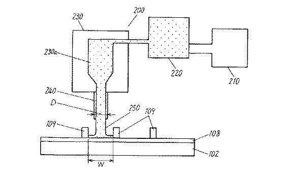
図5は、蛍光体層110R、110G、110Bを形成する際に用いるインキ塗布装置200の概略構成図である。図5に示すように、インキ塗布装置200は、サーバ210、加圧ポンプ220、ヘッダ230を備え、蛍光体インキを蓄えるサーバ210から供給される蛍光体インキは、加圧ポンプ220によりヘッダ230に加圧されて供給される。ヘッダ230にはインキ室230a及びノズル240が設けられており、加圧されてインキ室230aに供給された蛍光体インキは、ノズル240から連続的に吐出されるように構成されている。このノズル240の口径Dは、ノズルの目づまり防止のため、30μm以上で、かつ塗布の際の隔壁からのはみ出し防止のために隔壁109間の間隔W(約130μm〜200μm)以下にすることが望ましく、通常30μm〜130μmに設定される。
【0033】
ヘッダ230は、図示しないヘッダ走査機構によって直線的に駆動されるように構成されており、ヘッダ230を走査させるとともにノズル240から蛍光体インキ250を連続的に吐出することにより、背面ガラス基板102上の隔壁109間の溝に蛍光体インキが均一に塗布される。ここで、使用される蛍光体インキの粘度は25℃において、1500〜30000CPの範囲に保たれている。
【0034】
なお、上記サーバ210には図示しない攪拌装置が備えられており、その攪拌により蛍光体インキ中の粒子の沈殿が防止される。またヘッダ230は、インキ室230aやノズル240の部分も含めて一体成形されたものであり、金属材料を機器加工ならびに放電加工することによって作製されたものである。
【0035】
また、蛍光体層を形成する方法としては、上記方法に限定されるものではなく、例えばフォトリソ法、スクリーン印刷法及び蛍光体粒子を混合させたフィルムを配設する方法などの種々の方法を利用することができる。
【0036】
蛍光体インキは、各色蛍光体粒子、バインダー、溶媒とが混合され、1500〜50000センチポアズ(CP)となるように調合されたものであり、必要に応じて、界面活性剤、シリカ、分散剤(0.1〜5wt%)等を添加してもよい。
【0037】
この蛍光体インキに調合される赤色蛍光体としては、(Y、Gd)1-XBO3:EuX、またはY2-XO3:EuXで表される好ましい化合物が用いられる。これらは、その母体材料を構成するY元素の一部がEuに置換された化合物である。ここで、Y元素に対するEu元素の置換量Xは、0.05≦X≦0.20の範囲となることが好ましい。これ以上の置換量とすると、輝度は高くなるものの輝度劣化が著しくなることから実用上使用できにくくなると考えられる。一方、この置換量以下である場合には、発光中心であるEuの組成比率が低下し、輝度が低下して蛍光体として使用できなくなるためである。
【0038】
緑色蛍光体としては、表面が正に帯電した欠陥の少ないマグネトプラムバイト結晶構造を有するMMg1-xAl11O19:Mnx(ただし、MはCe、Laで、xの好ましい範囲は、0.1≦x≦1.0)あるいは、イットリア系の(Y1-a-yGda)BO3:Tby、(Y1-a-yGda)(Ga1-xAlx)3(BO3)4:Tby、(Y1-a-yGda)(Ga1-xAlx)3(BO3)4:Cey、Tby、(Y1-y)3(Ga1-xAlx)5O12:Tby、LaMg1-xAl11O19:Cex、Tbxで表される化合物及びこれら蛍光体の混合(イットリア系は一種以上でも良い)が用いられる。ここで、Gaに対するAlの置換量x、Yに対するGdの置換量a、Yに対するTbの置換量yは、それぞれ0.1≦x≦1.0、0≦a≦0.9、0.02≦y≦0.4の範囲となることが好ましい。Mgに対するCe、Tbの置換量は0.01≦x≦0.1の範囲が好ましい。
【0039】
青色蛍光体としては、Ba1-XMgAl10O17:EuX、またはBa1-x-ySryMgAl10O17:EuXで表される化合物が用いられる。Ba1-XMgAl10O17:EuX、Ba1-x-ySryMgAl10O17:EuXは、その母体材料を構成するBa元素の一部がEuあるいはSrに置換された化合物である。ここで、Ba元素に対するEu元素の置換量Xは、上記と同様の理由により、前者の青色蛍光体は0.03≦X≦0.20、0.1≦Y≦0.5の範囲となることが好ましい。
【0040】
これらの蛍光体の合成方法については後述する。蛍光体インキに調合されるバインダーとしては、エチルセルローズやアクリル樹脂を用い(インキの0.1〜10wt%を混合)、溶媒としては、α−ターピネオール、ブチルカービトールを用いることができる。なお、バインダーとして、PMAやPVAなどの高分子を、溶媒として、ジエチレングリコール、メチルエーテルなどの有機溶媒を用いることもできる。
【0041】
本実施の形態においては、蛍光体粒子には、固相焼成法、水溶液法、噴霧焼成法、水熱合成法により製造されたものが用いられる。
【0042】
▲1▼青色蛍光体
(Ba1-XMgAl10O17:EuXについて)
まず、混合液作製工程において、原料となる、硝酸バリウムBa(NO3)2、硝酸マグネシウムMg(NO3)2、硝酸アルミニウムAl(NO3)3、硝酸ユーロピウムEu(NO3)2をモル比が1−X:1:10:X(0.03≦X≦0.25)となるように混合し、これを水性媒体に溶解して混合液を作製する。この水性媒体にはイオン交換水、純水が不純物を含まない点で好ましいが、これらに非水溶媒(メタノール、エタノールなど)が含まれていても使用することができる。
【0043】
次に水和混合液を金あるいは白金などの耐食性、耐熱性を持つものからなる容器に入れて、例えばオートクレーブなどの加圧しながら加熱する事ができる装置を用い、高圧容器中で所定温度(100〜300℃)、所定圧力(0.2MPa〜10MPa)の下で水熱合成(12〜20時間)を行う。
【0044】
次に、この粉体を還元雰囲気下(例えば水素を5%、窒素を95%含む雰囲気)で、所定温度、所定時間(例えば、1350℃で2時間)焼成し次にこれを分級することにより所望の青色蛍光体Ba1-XMgAl10O17:EuXを得ることができる。次にこの粉体を水や炭化水素系ガスの吸着サイトを減少させるために、酸素−窒素中700℃〜1000℃でアニールして(Euの2価1部を3価にして)、酸素欠陥を取り除く。
【0045】
また、前記水和混合物を金あるいは、白金の容器に入れずに、この水和混合物をノズルから高温炉に吹き付けて蛍光体を合成する噴霧法によっても青色蛍光体を作製できる。
【0046】
(Ba1-x-ySryMgAl10O17:EuXについて)
この蛍光体は、上述したBa1-XMgAl10O17:EuXと原料が異なるのみで固相反応法で作製する。以下、その使用する原料について説明する。
【0047】
原料として、水酸化バリウムBa(OH)2、水酸化ストロンチウムSr(OH)2、水酸化マグネシウムMg(OH)2、水酸化アルミニウムAl(OH)3、水酸化ユーロピウムEu(OH)2を必要に応じたモル比となるように秤量し、これらをフラックスとしてのAlF3と共に混合し、所定の温度(1300℃〜1400℃)と焼成時間(12〜20時間)を経ることにより、Mg、Alを4価のイオンで置換したBa1-x-ySryMgAl10O17:EuXを得ることができる。この方法により、蛍光体粒子の平均粒径は、0.1μm〜3.0μm程度のものが得られる。
【0048】
次にこれを還元雰囲気下、例えば水素を5%、窒素を95%の雰囲気で所定の1000℃〜1600℃の温度で2時間焼成した後、空気分級機によって分級して蛍光体粉を作製する。次にこれを水や炭化水素系ガスの吸着サイトをなくすために、酸素−窒素中700℃〜1000℃でアニールして(Euの2価の1部を3価にして)酸素欠陥を取り除く。
【0049】
なお蛍光体の原料として、酸化物、硝酸塩、水酸化物を主に用いたが、Ba、Sr、Mg、Al、Eu、等の元素を含む有機金属化合物、例えば金属アルコキシド、やアセチルアセトン等を用いて、蛍光体を作製することもできる。
【0050】
▲2▼緑色蛍光体
(MMg1-xAl11O19:Mnx、(Y1-xGdx)Al3(BO3)4:Tbについて)
まず、マグネトプラムバイト結晶構造を有するアルミン酸塩系のMMg1-xAl11O19:Mnxについて、発光物質であるMnは、Mgと置換するため、前記化学式は、M(Mg1-xMnx)Al11O19(MはLa、Ce)と記述される。ここで(固相法で作製する場合)原料である、酸化ランタンLa2O3、酸化セリウムCe2O3、酸化マグネシウムMgO、酸化アルミニウムAl2O3、発光物質である炭酸マンガンMnCO3を、その組成がM(Mg1-xMnx)Al11O19となるように、必要に応じた酸化物のモル比と、xの値を決めて配合し、次に、少量のフラックス(AlF3、NH4F)とこれらの配合物を混合する。次に、これを950℃〜1300℃で空気中2時間焼成する。次に、これを凝集物がほぐれる程度に軽く粉砕後、これを窒素中あるいは窒素−水素中900℃〜1200℃で焼成し、これを粉砕した後、水や炭化水素ガスの吸着サイトを低減するため、酸素あるいは酸素−窒素中で500℃〜900℃でアニールして酸素欠陥を取り除き、正に帯電する緑色蛍光体を作製する。
【0051】
また、イットリウム系緑色蛍光体を作製する場合は、アルミン酸塩系と同様にして、原料となる酸化イットリウム(Y2O3)、酸化ガドリニウム(Gd2O3)、酸化ガリウム(Ga2O3)、酸化アルミニウム(Al2O3)、酸化硼素(B2O3)、及び発光物質である酸化テルビウム(Tb2O3)をそれぞれの蛍光体の組成に応じて配合し、少量のフラックスと共に混合した後、900℃〜1300℃で空気中で4時間焼成する。
【0052】
次に、これを凝集物がほぐれる程度に軽く粉砕した後、これを窒素中あるいは窒素−水素中で900℃〜1200℃で焼成し、これを粉砕した後、水や炭化水素ガスの吸着サイトを低減するため、酸素あるいは酸素−窒素中で500℃〜900℃でアニールして酸素欠陥を取り除き、正に帯電する緑色蛍光体を作製する。
【0053】
▲3▼赤色蛍光体
(Y、Gd)1-XBO3:EuXについて)
混合液作製工程において、原料である、硝酸イットリウムY2(NO3)3と水硝酸ガドリニウムGd2(NO3)3とホウ酸H3BO3と硝酸ユーロピウムEu2(NO3)3を混合し、モル比が1−X:2:X(0.05≦X≦0.20)(YとGdの比は65対35)となるように混合し、次にこれを空気中で1200℃〜1350℃で2時間熱処理した後、分級して赤色蛍光体を得る。赤色は空気中で焼成しているため、酸素−窒素中でアニールしなくても酸素欠陥が比較的少ないが、分級工程で欠陥が生じることがあり、アニールすることが好ましい。
【0054】
(Y2-XO3:EuXについて)
混合液作製工程において、原料である、硝酸イットリウムY2(NO3)3と硝酸ユーロピウムEu2(NO3)3を混合し、モル比が2−X:X(0.05≦X≦0.30)となるようにイオン交換水に溶解して混合液を作製する。
【0055】
次に、水和工程において、この水溶液に対して塩基性水溶液(例えば、アンモニア水溶液)を添加し、水和物を形成させる。
【0056】
その後、水熱合成工程において、この水和物とイオン交換水を白金や金などの耐食性、耐熱性を持つものからなる容器中に入れ、例えばオートクレーブを用いて高圧容器中で温度100〜300℃、圧力0.2M〜10MPaの条件下で3〜12時間水熱合成を行う。その後、得られた化合物の乾燥を行い、所望のY2- XO3:EuXが得られる。
【0057】
次に、この蛍光体を空気中で1300℃〜1400℃で2時間アニールした後分級して赤色蛍光体とする。この水熱合成工程により、得られる蛍光体は粒径が0.1μm〜2.0μm程度となり、かつその形状が球状となる。この粒径、形状は発光特性に優れた蛍光体層を形成するのに適している。
【0058】
なお、これら赤色蛍光体は空気中で焼成するため、酸素欠陥が少なくしたがって、水や炭化水素系ガスの吸着も少ない。
【0059】
なお、上述したPDP100の赤色の蛍光体層110Rについては、従来用いられてきた蛍光体を用い、Gについては、表面が正に帯電したM(Mg1-xMnx)Al11O19(Mは、La、Ceのいずれか一種)のアルミン酸塩系の緑色蛍光体と、同じく(+)帯電を有する(Y1-xGdx)BO3:Tb、(Y1-xGdx)Al3(BO3)4:Tb、(Y1-xGdx)Al3(BO3)4:Ce、Tb、Y3Al3Ga2O12:Tb、LaMg1-xAl11O19:Cex、Tbxのイットリア含有の緑色蛍光体を用い、Bについては、BaMgAl10O17:EuあるいはBaSrAl10O17:Euを使用した。特に、従来のZn2SiO4:Mn緑色蛍光体は、本発明の緑色蛍光体と比べて、負に帯電しているため、蛍光体工程中でノズルの目づまりが起こりやすく、また緑色を発光させた時の輝度は低下する傾向があったが、本発明にかかる製造方法により製造された緑色蛍光体を使用すれば、緑色セルの蛍光体塗布工程中でのノズルの目づまりがなく、またパネルの色ずれや輝度劣化及びアドレス放電ミスも起こらない。したがって、白表示の時の輝度を上げることができる。
【0060】
以下、本発明のプラズマディスプレイ装置の性能を評価するために、上記実施の形態に基づくサンプルを作製し、そのサンプルについて性能評価実験を行った。
【0061】
作製した各プラズマディスプレイ装置は、42インチの大きさを持ち(リブピッチ150μmのHD−TV仕様)、誘電体ガラス層の厚みは20μm、MgO保護層の厚みは0.5μm、表示電極と表示スキャン電極の間の距離は0.08mmとなるように作製した。また、放電空間に封入される放電ガスは、ネオンを主体にキセノンガスを5%以上90%以下で混合したガスであり、放電ガスとして66.5KPaの圧力で封入したものである。
【0062】
サンプル1〜6のPDPに用いる蛍光体粒子には、正に帯電するアルミン酸塩系のM(Mg1-xMnx)Al11O19(ただし、MはLa、Ceの内のいずれか一種)の緑色蛍光体と、BaMgAl10O17:Euあるいは(Ba、Sr)MgAl10O17:Euの青色蛍光体と、(Y、Gd)BO3:EuあるいはY2O3:Euの赤色蛍光体とを用いた。また、それぞれのa、xの値及びMの種類を表1に示す。
【0063】
サンプル7〜10、12、13のPDPに用いる蛍光体粒子には、正に帯電するアルミン酸塩系のM(Mg1-xMnxAl11O19(ただし、La、Ceの内のいずれか一種)とイットリア系の(Y1-b-yGdb)(Ga1-xAlx)(BO3)4:Tby、(Y1-b-yGdb)3(Ga1-xAlx)5O12:Cey、Tby及び(Y1-b-yGdb)BO3:Tbyの緑色蛍光体との混合蛍光体と、(Ba、Sr)MgAl10O17:EuあるいはBaMgAl10O17:Eu青色蛍光体と、Y2O3:Euあるいは(Y、Gd)BO3:Euの赤色蛍光体とを用いた。また、それぞれのa、x、b、yの値及びMの種類を表1に示す。
【0064】
サンプル11のPDPに用いる蛍光体粒子には、正に帯電するアルミン酸塩系のM(Mg1-xMnxAl11O19(ただし、La、Ceの内のいずれか一種)とマグネトプラムバイト系のLaMg1-xAl11O19:Cex、Tbxの緑色蛍光体との混合蛍光体と、(Ba、Sr)MgAl10O17:Euあるいは、BaMgAl10O17:Euの青色蛍光体と、Y2O3:Euあるいは(Y、Gd)BO3:Eu赤色蛍光体とを用いた。また、それぞれのa、x、b、yの値及びMの種類を表1に示す。
【0065】
サンプル14〜19(比較例)のPDPに用いる緑色には、従来例のZn2SiO4:Mn、BaAl12O17:Mn、BaMgAl14O23:Eu、Mn、LaPO4:Tbの内のいずれか一種が入った蛍光体を、青色蛍光体にはBaMgAl10O17:Euを、赤色蛍光体には(Y、Gd)BO3:Euを用いたパネルである。また、それぞれの蛍光体組成を表1に示す。
【0066】
【表1】
(実験1)
作製されたサンプル1〜13及び比較サンプル14〜19について、先ず作製した緑色蛍光体をグローオフ法を用いて還元鉄紛に対する帯電量を調べた(照明学会誌 第76巻第10号 平成4年 PP16〜27)。
【0068】
その結果Zn2SiO4:Mnが含まれるサンプル14、16は、負に帯電しているがそれ以外のサンプルは正に帯電していた。
【0069】
(実験2)
作製したパネル中の蛍光体(青、緑、赤)を取り出し、水、CO、CO2あるいは炭化水素の吸着量をTDS(昇温脱離ガス質量分析法)にて測定した。試料は作製したパネル内の蛍光体100ミリグラム(mg)を採取し、それを室温から1000℃まで昇温して、出てきた水及び炭化水素系ガスの総量を測定し、サンプル1の水及び炭化水素系ガスの量を1と規格化し、各サンプルの量と比較した。
【0070】
(実験3)
パネル製造工程後のパネルの輝度(全白、緑、青、赤)及び色温度を輝度計を用いて測定した。
【0071】
(実験4)
パネルを点灯した時の全白表示時の輝度劣化、色温度測定は、PDPに電圧185V、周波数200kHzの放電維持パルスを1000時間連続して印加し、その前後におけるパネル輝度色温度を測定し、そこから輝度劣化変化率(<〔印加後の輝度−印加前の輝度〕/印加前の輝度>*100)と色温度の変化率を求めた。また、アドレス放電時のアドレスミスについては画像を見てちらつきがあるかないかで判断し、1ヶ所でもあれば、ありとしている。
【0072】
これら実験1〜4の緑色の輝度及び輝度劣化変化率、アドレスミスの有無についての結果を表2に示す。
【0073】
【表2】
表2に示すように、比較サンプル14、15、16、17、18、19における緑色蛍光体は、サンプル14が、Zn2SiO4:Mnと(Y、Gd)BO3:Tbの組み合わせ、サンプル15がBaAl12O17:Mnと(Y、Gd)BO3の組み合わせ、サンプル16がZn2SiO4:Mnのみ、サンプル17がBaMgAl14O23:Eu、Mnのみ、サンプル18がBaAl12O19:Mnのみ、サンプル19がBaAl12O17:MnとLaPO4:Tbの組み合わせで、青色蛍光体にBaMgAl10O17:Euを使用したサンプルである。そのためこれらの蛍光体に水や炭化水素系ガスが多く吸着している。特に、水の吸着が本発明の実施の形態と比較して2〜3倍多く、絶対量は水の1/5〜1/10であるが、炭化水素も2〜3倍多くなっている。
【0075】
したがって、比較例14〜19は放電中(駆動中)緑色や青色の輝度の低下が大きく低下し、Xe分圧が10%を超えると特にアドレスミスが多発する。特に、サンプル14、16は緑色にZn2SiO4:Mnを使用しているため、負に蛍光体が帯電しているのに加え、水や炭化水素の吸着が多いため、アドレスミスや紫外線(147nm)や放電維持パルスによる輝度劣化が大きい。
【0076】
また、サンプル17、18、19は緑色にBaMgAl14O23:Mn、Eu、BaAl12O19:Mn、LaPO4:Tb等の水や炭化水素ガスを吸着し易い蛍光体を用いているため、アドレスミスや放電による劣化が特に大きい。
【0077】
これに対し、サンプル1〜13の緑色、青色、赤色の組み合わせパネルはすべて、紫外線(147nm)や維持放電パルスによる各色の輝度変化率が少なく、従って色温度の低下やアドレスミスあるいは蛍光体塗布時のノズルの目づまりもない。これは、従来の水や炭化水素が吸着し易い緑色蛍光体に変えて、Alを含有する、マグネトプラムバイト結晶構造のM(Mg1-xMnx)Al11O19あるいはYあるいはAlを含有する(Y1-b-yGdb)(Ga1-xAlx)3(BO3)4:Tby、(Y1-b-yGd)3(Ga1-xAlx)3(Ga1-xAlx)5O12:Ce、Tby、(Y1-b-yGdb)BO3:Tby、LaMg1-xAl11O19:Cex、Tbxの単独、または組み合わせで使用することで、パネル中の水や炭化水素の発生が抑制され、放電による輝度劣化やMgOの変質によるアドレスミスがなくなったためである。
【0078】
【発明の効果】
以上述べてきたように本発明によれば、前面パネルと背面パネルとの間に、5%を超えるXeを含む放電ガスを封入した放電空間を形成するとともに、放電セルを複数配列して設け、かつ各放電セルに配設された蛍光体層を紫外線により励起することにより発光するプラズマディスプレイパネルを備えたプラズマディスプレイ装置であって、前記蛍光体層の緑色蛍光体は、一般式MMg1-xAl11O19:Mnx(ただし、MはLa、Ceの内のいずれか一種)と、一般式(Y1-a-yGda)(Ga1-xAlx)3(BO3)4:Tby、一般式(Y1-a-yGda)(Ga1-xAlx)3(BO3)4:Cey、Tby、一般式(Y1-a-yGda)BO3:Tby、一般式LaMg1-xAl11O19:Cex、Tbxの中から選ばれるいずれか一種の蛍光体、または一種以上の蛍光体とを混合してなる混合蛍光体であり、かつ前記一般式MMg 1-x Al 11 O 19 :Mn x において、xが0.01≦x≦0.1であることを特徴とすることにより、各色蛍光体結晶の帯電状態を正にし、特に緑色蛍光体に水分や炭化水素の吸着が少なく電子放出係数の比較的大きいAlやYを母体とするマグネトプラムバイト結晶構造を有するアルミン酸塩系やイットリア系の蛍光体粒子で、緑色蛍光体を構成することによって、パネル中のXe分圧が高くなっても、パネルの輝度及び色温度の低下がなく、アドレスミスのない信頼性の高いパネルを実現することができる。
【図面の簡単な説明】
【図1】本発明の一実施の形態によるPDPの前面ガラス基板を除いた状態を示す平面図
【図2】同じくPDPの画像表示領域の構造を示す斜視図
【図3】本発明の一実施の形態によるプラズマディスプレイ装置を示すブロック図
【図4】本発明のPDPの画像表示領域の構造を示す断面図
【図5】本発明において、蛍光体層を形成する際に用いるインキ塗布装置の概略構成図
【符号の説明】
100 PDP
101 前面ガラス基板
103 表示電極
104 表示スキャン電極
105 誘電体ガラス層
106 MgO保護層
107 アドレス電極
108 誘電体ガラス層
109 隔壁
110R 蛍光体層(赤)
110G 蛍光体層(緑)
110B 蛍光体層(青)
122 放電空間[0001]
BACKGROUND OF THE INVENTION
The present invention relates to a plasma display device used for image display such as a television.
[0002]
[Prior art]
2. Description of the Related Art In recent years, among color display devices used for image display such as computers and televisions, display devices using plasma display panels (hereinafter referred to as PDPs) are attracting attention as color display devices that are large, thin, and lightweight. Has been.
[0003]
The PDP performs full color display by additively mixing so-called three primary colors (red, green, and blue). In order to perform this full-color display, the PDP is provided with a phosphor layer that emits each of the three primary colors red (R), green (G), and blue (B), and the phosphor constituting the phosphor layer. The particles are excited by ultraviolet rays generated in the discharge cell of the PDP, and generate visible light of each color.
[0004]
Examples of the compound used for the phosphors of the respective colors include (Y, Gd) BO that emits red light and is positively (+) charged.Three: Eu3+Or Y2OThree: Eu3+Zn that emits green light and is negatively charged (-)2SiOFour: Mn2+BaMgAl that emits blue light and is positively charged (+)TenO17: Eu2+Is known (see, for example, Non-Patent Document 1).
[0005]
Each of these phosphors is produced by mixing a predetermined raw material and then performing a solid phase reaction by firing at a high temperature of 1000 ° C. or more (see, for example, Non-Patent Document 2).
[0006]
Also, in the combination of red, green and blue of the conventional phosphor, only green is charged (-), so the amount of charge stored on the phosphor is greatly different from red and blue, and a discharge error occurs. There is a problem that it is easy.
[0007]
Therefore, in order to make the charge amount as close to red and blue as possible, YBO has (+) charge.Three: Tb and Zn2SiOFour: Method of eliminating discharge mistakes by mixing Mn (Patent Document 1) and BaAl having (+) electrification12O19: Mn, BaMgAl14Otwenty three: (Y, Gd) BO having the same (+) charge as MnThree: Tb, LaPOFour: Trying to improve discharge characteristics and luminance degradation by combining Tb (Patent Document 2) has been considered.
[0008]
[Non-Patent Document 1]
O plus E. February 1996 No. 195 pp99-100
[Non-Patent Document 2]
Phosphor Handbook P219, 225 Ohm
[Patent Document 1]
JP 2001-236893 A
[Patent Document 2]
JP 2003-7215 A
[0009]
[Problems to be solved by the invention]
However, when a high-luminance PDP is produced by increasing the concentration of Xe gas in the PDP using a combination of conventional phosphor materials, there is a problem described below particularly for the green phosphor.
[0010]
BaMgAl in blueTenO17: Eu, Zn on green2SiOFour: Mn, red (Y, Gd) BOThree: Eu, Y2OThree: The panel produced by the combination of Eu has positive (+) charge on the surface of the blue phosphor and the red phosphor among these phosphors.2SiOFour: In the case of a green phosphor made of Mn, SiO with respect to ZnO in the production of the phosphor2Is the stoichiometric ratio (2ZnO / SiO2) Than SiO2(1.5ZnO / SiO2) Because Zn2SiOFour: The surface of Mn crystal is SiO2The surface of the phosphor is negatively charged (−). Generally, when a negatively charged phosphor and a positive (+) charged phosphor are mixed in a PDP, negative (-) occurs when the panel is driven, especially when the entire surface is erased after the entire surface is turned on. There is a problem that negative charges remain only on the charged phosphor, and that when a voltage for display is applied, discharge variation or a discharge error that does not cause discharge occurs. In particular, it has been found that these problems become significant when the amount of Xe in the discharge gas is 5% or more in order to improve the brightness and efficiency of the PDP.
[0011]
In addition, Zn used in particular for green2SiOFour: The surface of Mn is SiO2Since it is covered with, it is in a state where it is very easy to adsorb gas. Zn2SiOFour: Mn is water (H2O), CO, CO2Or hydrocarbon gas (CxHy) Is adsorbed on the surface of MgO and is deteriorated in the discharge characteristics. These gases are blue phosphor BaMgAlTenO17: Eu or Zn as green phosphor2SiOFour: Adsorbed to the surface of Mn, causing a surface reaction there, causing a problem that luminance deterioration and a chromaticity y value increase when the color is blue, and color shift occurs due to a decrease in the color temperature of the panel.
[0012]
On the other hand, the green phosphor Zn whose surface is negatively charged2SiOFour: Mn and ReBO, a positively charged green phosphorThree: Tb (Re is a rare earth element: Sc, Y, La, Ce, Gd) to make the phosphor layer appear to be positively (+) charged, and blue and red are respectively positively charged BaMgAlTenO17: Eu, (Y, Gd) BOThree: A panel using a combination using Eu is considered, and discharge errors due to charge imbalance are improved to some extent, but discharge errors increase as the Xe gas concentration increases.
[0013]
In addition to this discharge mistake, this green combination is still H2O and CxHyZn which is easy to adsorb2SiOFourAs described above, H is released into the panel during discharge.2O, CO, CO2Or CxHyMgO deteriorates due to the gas, and discharge characteristics such as variations in discharge and discharge errors occur. On top of that these gases and BaMgAlTenO17: Eu, Zn2SiOFour: There existed a subject that a brightness | luminance degradation and a color shift produced by the surface reaction with Mn.
[0014]
Furthermore, as a green phosphor, (-) charged Zn2SiOFourInstead of all (+) charged BaAl12O17: Mn, BaMgAlTenO17: Mn, (Y, Gd) BOThree: Tb or LaPOFour: Any one of the five phosphors of Tb is used in combination as green, and blue with BaMgAlTenO17: Eu, red (Y, Gd) BOThree: Eu and Y2OThree: All combinations using Eu are (+) electrification, and discharge errors can be solved to some extent.
[0015]
However, when the amount of Xe in the discharge gas exceeds 5% (especially when it exceeds 10%), the discharge voltage rises, resulting in a problem that discharge errors and discharge variations increase. In addition to the deterioration of the discharge characteristics, among these green phosphors, BaAl having a β-alumina crystal structure in which layered defects are present.12O19: Mn, BaMgAl14Otwenty three: Mn or LaPOFour: Tb is still water (H2O) and hydrocarbons (CxHy) Is easily adsorbed, and H during panel aging2O or CxHyIs emitted into the panel, the luminance degradation is severe due to the chemical reaction on the surface of these phosphors, and the deterioration when the panel is turned on for a long time becomes large. There is a problem that a color shift of the panel occurs such that the color temperature is lowered and the screen becomes yellowish.
[0016]
The present invention has been made in view of such a problem. All the charges are positive (+) and water (H2O), CO (carbon monoxide), CO2(Carbon dioxide) or hydrocarbon (CxHyIt is an object of the present invention to provide a plasma display device including a green phosphor with little adsorption or reaction.
[0017]
[Means for Solving the Problems]
In order to achieve this object, the present invention forms a discharge space in which a discharge gas containing Xe exceeding 5% is enclosed between a front panel and a back panel, and a plurality of discharge cells are arranged, and A plasma display device including a plasma display panel that emits light by exciting a phosphor layer disposed in each discharge cell with ultraviolet rays, wherein the green phosphor of the phosphor layer has a general formula MMg1-xAl11O19: Mnx(Where M is one of La and Ce) and the general formula (Y1-ayGda) (Ga1-xAlx)Three(BOThree)Four: Tby, General formula (Y1-ayGda) (Ga1-xAlx)Three(BOThree)Four: Cey, Tby, General formula (Y1-ayGda) BOThree: Tby, General formula LaMg1-xAl11O19: Cex, TbxOne kind of phosphor selected from the above, or a mixed phosphor formed by mixing one or more kinds of phosphorsAnd the general formula MMg 1-x Al 11 O 19 : Mn x X is 0.01 ≦ x ≦ 0.1It is characterized by this.
[0018]
According to such a configuration, since all the charges are (+) charged, the charges stored on the phosphor are substantially equal, so that there is no discharge variation in R, G, B during address discharge, thereby eliminating a discharge error. Unlike the conventional example, the green phosphor has a high electron emission amount γ such as Al, Y, etc., and the host itself is composed of an oxide with a small amount of adsorption of water or hydrocarbon gas. Even when the amount of the panel is 5% or more, the discharge voltage rises little as in the case of using the conventional green phosphor. Therefore, even if the Xe partial pressure is increased to increase the brightness, the address discharge voltage does not increase so much when the panel is driven, so that the number of discharge errors is reduced.
[0019]
Also, Zn containing no conventional Al or Y2SiOFour: BaAl with β-alumina crystal structure with many Mn and crystal defects12O19: Mn or BaMgAl14Otwenty three: LaMg of magnetoplumbite crystal structure with few defects in the crystal instead of Mn and Eu1-xAl11O19: MnxSince yttrium borate and yttrium aluminum phosphors are used, the amount of adsorption of water and hydrocarbon gas is reduced. Therefore, even if the amount of Xe gas is 5% or more, the increase in the discharge voltage due to the separation of the adsorbed gas is reduced as in the case of using the conventional green phosphor. Since the voltage of the address discharge at the time does not rise so much, discharge mistakes are reduced.
[0020]
DETAILED DESCRIPTION OF THE INVENTION
Hereinafter, a plasma display device according to an embodiment of the present invention will be described with reference to the drawings.
[0021]
FIG. 1 is a schematic plan view of the PDP with the front glass substrate removed, and FIG. 2 is a partial sectional perspective view of the image display area of the PDP. In FIG. 1, the number of display electrode groups, display scan electrode groups, address electrode groups, and the like are partially omitted for easy understanding. The structure of the PDP will be described with reference to both drawings.
[0022]
As shown in FIG. 1, the
[0023]
As shown in FIG. 2, the
[0024]
When driving the plasma display device, as shown in FIG. 3, a
[0025]
Next, a manufacturing method for the above-described
[0026]
In the front panel, first, each of the
[0027]
The
[0028]
The MgO
[0029]
The back panel is formed in such a manner that M address
[0030]
FIG. 4 is a cross-sectional view of the
[0031]
The front panel and the back panel manufactured in this way are overlapped so that each electrode of the front panel and the address electrode of the back panel are orthogonal to each other, and a sealing glass is interposed on the periphery of the panel. It seals by baking for 15 minutes at about 0 degreeC, and forming the
[0032]
FIG. 5 is a schematic configuration diagram of the
[0033]
The
[0034]
The
[0035]
In addition, the method for forming the phosphor layer is not limited to the above-described method, and various methods such as a photolithographic method, a screen printing method, and a method of disposing a film mixed with phosphor particles are used. can do.
[0036]
The phosphor ink is prepared by mixing phosphor particles of various colors, a binder, and a solvent to be 1500 to 50000 centipoise (CP). If necessary, a surfactant, silica, a dispersant ( 0.1 to 5 wt%) may be added.
[0037]
As red phosphors to be prepared in this phosphor ink, (Y, Gd)1-XBOThree: EuXOr Y2-XOThree: EuXA preferred compound represented by the formula: These are compounds in which part of the Y element constituting the base material is substituted with Eu. Here, the substitution amount X of the Eu element with respect to the Y element is preferably in the range of 0.05 ≦ X ≦ 0.20. If the substitution amount is larger than this, the luminance is increased, but the luminance is significantly deteriorated. On the other hand, when the amount is less than this substitution amount, the composition ratio of Eu, which is the emission center, is lowered, the luminance is lowered, and the phosphor cannot be used.
[0038]
As the green phosphor, MGg having a magnetoplumbite crystal structure with a positively charged surface and few defects1-xAl11O19: Mnx(However, M is Ce, La, and the preferred range of x is 0.1 ≦ x ≦ 1.0) or yttria-based (Y1-ayGda) BOThree: Tby, (Y1-ayGda) (Ga1-xAlx)Three(BOThree)Four: Tby, (Y1-ayGda) (Ga1-xAlx)Three(BOThree)Four: Cey, Tby, (Y1-y)Three(Ga1-xAlx)FiveO12: Tby, LaMg1-xAl11O19: Cex, TbxAnd a mixture of these phosphors (one or more yttria compounds may be used). Here, the substitution amount x of Al for Ga, the substitution amount a of Gd for Y, and the substitution amount y of Tb for Y are 0.1 ≦ x ≦ 1.0, 0 ≦ a ≦ 0.9, and 0.02, respectively. It is preferable to be in the range of ≦ y ≦ 0.4. The substitution amount of Ce and Tb for Mg is preferably in the range of 0.01 ≦ x ≦ 0.1.
[0039]
As the blue phosphor, Ba1-XMgAlTenO17: EuXOr Ba1-xySryMgAlTenO17: EuXThe compound represented by these is used. Ba1-XMgAlTenO17: EuX, Ba1-xySryMgAlTenO17: EuXIs a compound in which a part of the Ba element constituting the base material is substituted with Eu or Sr. Here, the substitution amount X of Eu element with respect to Ba element is in the range of 0.03 ≦ X ≦ 0.20 and 0.1 ≦ Y ≦ 0.5 for the former blue phosphor for the same reason as above. It is preferable.
[0040]
A method for synthesizing these phosphors will be described later. Ethyl cellulose or acrylic resin can be used as the binder to be prepared for the phosphor ink (mixed with 0.1 to 10 wt% of the ink), and α-terpineol or butyl carbitol can be used as the solvent. A polymer such as PMA or PVA can be used as the binder, and an organic solvent such as diethylene glycol or methyl ether can be used as the solvent.
[0041]
In the present embodiment, phosphor particles manufactured by a solid phase firing method, an aqueous solution method, a spray firing method, or a hydrothermal synthesis method are used.
[0042]
(1) Blue phosphor
(Ba1-XMgAlTenO17: EuXabout)
First, barium nitrate Ba (NO, which is a raw material in the mixed liquid preparation step)Three)2, Magnesium nitrate Mg (NOThree)2, Aluminum nitrate Al (NOThree)Three, Europium nitrate Eu (NOThree)2Are mixed so that the molar ratio is 1-X: 1: 10: X (0.03 ≦ X ≦ 0.25), and this is dissolved in an aqueous medium to prepare a mixed solution. In this aqueous medium, ion-exchanged water and pure water are preferable in that they do not contain impurities, but they can be used even if they contain a non-aqueous solvent (such as methanol or ethanol).
[0043]
Next, the hydration liquid mixture is put in a container having corrosion resistance and heat resistance such as gold or platinum, and is heated in a high pressure container at a predetermined temperature (100, for example) using an apparatus such as an autoclave. Hydrothermal synthesis (12 to 20 hours) under a predetermined pressure (0.2 MPa to 10 MPa).
[0044]
Next, the powder is fired in a reducing atmosphere (for example, an atmosphere containing 5% hydrogen and 95% nitrogen) at a predetermined temperature for a predetermined time (for example, 2 hours at 1350 ° C.), and then classified. Desired blue phosphor Ba1-XMgAlTenO17: EuXCan be obtained. Next, this powder is annealed in oxygen-nitrogen at 700 ° C. to 1000 ° C. in order to reduce the adsorption sites of water and hydrocarbon gas (by making Eu divalent 1 part trivalent) to produce oxygen defects. Remove.
[0045]
A blue phosphor can also be produced by a spraying method in which a phosphor is synthesized by spraying the hydrated mixture from a nozzle to a high-temperature furnace without placing the hydrated mixture in a gold or platinum container.
[0046]
(Ba1-xySryMgAlTenO17: EuXabout)
This phosphor is the Ba described above.1-XMgAlTenO17: EuXIt is prepared by the solid phase reaction method only with different raw materials. Hereinafter, the raw materials used will be described.
[0047]
As raw material, barium hydroxide Ba (OH)2, Strontium hydroxide Sr (OH)2, Magnesium hydroxide Mg (OH)2, Aluminum hydroxide Al (OH)Three, Europium hydroxide Eu (OH)2Are weighed so as to have a molar ratio according to need, and these are AlF as a flux.ThreeBa, in which Mg and Al are substituted with tetravalent ions by passing through a predetermined temperature (1300 ° C. to 1400 ° C.) and firing time (12 to 20 hours).1-xySryMgAlTenO17: EuXCan be obtained. By this method, phosphor particles having an average particle diameter of about 0.1 μm to 3.0 μm are obtained.
[0048]
Next, after baking this in a reducing atmosphere, for example, in an atmosphere of 5% hydrogen and 95% nitrogen at a predetermined temperature of 1000 ° C. to 1600 ° C. for 2 hours, it is classified by an air classifier to produce phosphor powder. . Next, in order to eliminate the adsorption sites of water and hydrocarbon gas, this is annealed at 700 ° C. to 1000 ° C. in oxygen-nitrogen (by making the bivalent part of Eu trivalent) to remove oxygen defects.
[0049]
In addition, although oxide, nitrate, and hydroxide were mainly used as the raw material of the phosphor, organometallic compounds containing elements such as Ba, Sr, Mg, Al, Eu, such as metal alkoxide, acetylacetone, and the like were used. Thus, a phosphor can be produced.
[0050]
(2) Green phosphor
(MGg1-xAl11O19: Mnx, (Y1-xGdx) AlThree(BOThree)Four: About Tb)
First, an aluminate-based MGg having a magnetoplumbite crystal structure1-xAl11O19: MnxFor Mn, which is a luminescent material, substitutes Mg, the chemical formula is M (Mg1-xMnx) Al11O19(M is La, Ce). Here (when produced by a solid phase method), the raw material, lanthanum oxide La2OThree, Cerium oxide Ce2OThree, Magnesium oxide MgO, aluminum oxide Al2OThree, Manganese carbonate MnCO, a luminescent materialThreeWith a composition of M (Mg1-xMnx) Al11O19So that the molar ratio of oxides and the value of x are determined and blended, and then a small amount of flux (AlFThree, NHFourF) and these blends are mixed. Next, this is baked in air at 950 ° C. to 1300 ° C. for 2 hours. Next, this is lightly pulverized to such an extent that the agglomerates are loosened, and then baked at 900 ° C. to 1200 ° C. in nitrogen or nitrogen-hydrogen. After pulverizing this, the adsorption sites of water and hydrocarbon gas are reduced. Therefore, an oxygen defect is removed by annealing at 500 ° C. to 900 ° C. in oxygen or oxygen-nitrogen to produce a positively charged green phosphor.
[0051]
Moreover, when producing an yttrium-based green phosphor, the raw material yttrium oxide (Y2OThree), Gadolinium oxide (Gd2OThree), Gallium oxide (Ga2OThree), Aluminum oxide (Al2OThree), Boron oxide (B2OThree), And terbium oxide (Tb) which is a luminescent material2OThree) According to the composition of each phosphor, mixed with a small amount of flux, and then fired in the air at 900 ° C. to 1300 ° C. for 4 hours.
[0052]
Next, this is lightly pulverized to such an extent that the agglomerates are loosened, and then baked at 900 ° C. to 1200 ° C. in nitrogen or nitrogen-hydrogen. After pulverizing this, water and hydrocarbon gas adsorption sites are formed. In order to reduce this, an oxygen defect is removed by annealing at 500 ° C. to 900 ° C. in oxygen or oxygen-nitrogen to produce a positively charged green phosphor.
[0053]
(3) Red phosphor
(Y, Gd)1-XBOThree: EuXabout)
Yttrium nitrate Y, which is a raw material in the mixed liquid preparation process2(NOThree)ThreeAnd gadolinium nitrate Gd2(NOThree)ThreeAnd boric acid HThreeBOThreeAnd europium nitrate Eu2(NOThree)ThreeAnd mixed so that the molar ratio is 1-X: 2: X (0.05 ≦ X ≦ 0.20) (the ratio of Y to Gd is 65 to 35), After heat treatment at 1200 to 1350 ° C. for 2 hours, classification is performed to obtain a red phosphor. Since red is baked in the air, oxygen defects are relatively few even without annealing in oxygen-nitrogen, but defects may occur in the classification step, and annealing is preferable.
[0054]
(Y2-XOThree: EuXabout)
Yttrium nitrate Y, which is a raw material in the mixed liquid preparation process2(NOThree)ThreeAnd europium nitrate Eu2(NOThree)ThreeAre mixed in ion-exchanged water so as to have a molar ratio of 2-X: X (0.05 ≦ X ≦ 0.30) to prepare a mixed solution.
[0055]
Next, in the hydration step, a basic aqueous solution (for example, an aqueous ammonia solution) is added to this aqueous solution to form a hydrate.
[0056]
Thereafter, in the hydrothermal synthesis step, the hydrate and ion-exchanged water are placed in a container having corrosion resistance and heat resistance such as platinum or gold, and the temperature is set to 100 to 300 ° C. in a high pressure container using, for example, an autoclave. The hydrothermal synthesis is carried out for 3 to 12 hours under the conditions of pressure 0.2 M to 10 MPa. Thereafter, the obtained compound is dried to obtain the desired Y2- XOThree: EuXIs obtained.
[0057]
Next, this phosphor is annealed in air at 1300 ° C. to 1400 ° C. for 2 hours and then classified to obtain a red phosphor. The phosphor obtained by this hydrothermal synthesis step has a particle size of about 0.1 μm to 2.0 μm and a spherical shape. The particle size and shape are suitable for forming a phosphor layer having excellent light emission characteristics.
[0058]
Since these red phosphors are fired in the air, there are few oxygen defects, and therefore, there is little adsorption of water or hydrocarbon gas.
[0059]
For the red phosphor layer 110R of the
[0060]
Hereinafter, in order to evaluate the performance of the plasma display device of the present invention, a sample based on the above embodiment was produced, and a performance evaluation experiment was performed on the sample.
[0061]
Each produced plasma display device has a size of 42 inches (HD-TV specification with a rib pitch of 150 μm), the thickness of the dielectric glass layer is 20 μm, the thickness of the MgO protective layer is 0.5 μm, the display electrode and the display scan electrode. The distance between them was made to be 0.08 mm. The discharge gas sealed in the discharge space is a gas in which xenon gas is mixed at 5% to 90% mainly with neon, and is sealed at a pressure of 66.5 KPa as a discharge gas.
[0062]
The phosphor particles used in the PDPs of
[0063]
The phosphor particles used in the PDPs of Samples 7 to 10, 12, and 13 include positively charged aluminate-based M (Mg1-xMnxAl11O19(However, any one of La and Ce) and yttria (Y1-byGdb) (Ga1-xAlx) (BOThree)Four: Tby, (Y1-byGdb)Three(Ga1-xAlx)FiveO12: Cey, TbyAnd (Y1-byGdb) BOThree: TbyPhosphor mixed with green phosphor of (Ba, Sr) MgAlTenO17: Eu or BaMgAlTenO17: Eu blue phosphor and Y2OThree: Eu or (Y, Gd) BOThree: Eu red phosphor. Table 1 shows the values of a, x, b, and y and the types of M.
[0064]
The phosphor particles used in the PDP of sample 11 include positively charged aluminate-based M (Mg1-xMnxAl11O19(However, either La or Ce) and magnetoplumbite LaMg1-xAl11O19: Cex, TbxPhosphor mixed with green phosphor of (Ba, Sr) MgAlTenO17: Eu or BaMgAlTenO17: Eu blue phosphor and Y2OThree: Eu or (Y, Gd) BOThree: Eu red phosphor was used. Table 1 shows the values of a, x, b, and y and the types of M.
[0065]
The green color used for the PDPs of samples 14 to 19 (comparative examples) is Zn in the conventional example.2SiOFour: Mn, BaAl12O17: Mn, BaMgAl14Otwenty three: Eu, Mn, LaPOFour: Phosphor containing any one of Tb, and BaMgAl for blue phosphorTenO17: Eu, (Y, Gd) BO for red phosphorThree: A panel using Eu. In addition, Table 1 shows the respective phosphor compositions.
[0066]
[Table 1]
(Experiment 1)
With respect to the produced
[0068]
As a result, Zn2SiOFour: Samples 14 and 16 containing Mn were negatively charged, but the other samples were positively charged.
[0069]
(Experiment 2)
Take out the phosphors (blue, green, red) in the manufactured panel, and use water, CO, CO2Alternatively, the amount of adsorbed hydrocarbon was measured by TDS (Temperature Desorption Gas Mass Spectrometry). As a sample, 100 milligrams (mg) of the phosphor in the manufactured panel was collected, and the temperature was raised from room temperature to 1000 ° C., and the total amount of water and hydrocarbon-based gas that came out was measured. The amount of hydrocarbon gas was normalized to 1 and compared with the amount of each sample.
[0070]
(Experiment 3)
The luminance (total white, green, blue, red) and color temperature of the panel after the panel manufacturing process were measured using a luminance meter.
[0071]
(Experiment 4)
Luminance degradation and color temperature measurement when displaying all white when the panel is lit, a discharge sustaining pulse having a voltage of 185 V and a frequency of 200 kHz is continuously applied to the PDP for 1000 hours, and the panel luminance color temperature before and after the measurement is measured. From this, the luminance deterioration change rate (<[luminance after application-luminance before application] / luminance before application> * 100) and the change rate of the color temperature were determined. In addition, an address miss at the time of address discharge is determined by checking whether there is a flicker by looking at the image, and if there is even one place, it is determined.
[0072]
Table 2 shows the results of
[0073]
[Table 2]
As shown in Table 2, the green phosphors in Comparative Samples 14, 15, 16, 17, 18, 192SiOFour: Mn and (Y, Gd) BOThree: Tb combination, sample 15 is BaAl12O17: Mn and (Y, Gd) BOThreeSample 16 is a combination of2SiOFour: Mn only, sample 17 is BaMgAl14Otwenty three: Eu, Mn only, sample 18 is BaAl12O19: Mn only, sample 19 is BaAl12O17: Mn and LaPOFour: A combination of Tb and blue phosphor with BaMgAlTenO17: A sample using Eu. Therefore, a lot of water and hydrocarbon gas are adsorbed on these phosphors. In particular, the adsorption of water is 2 to 3 times greater than that of the embodiment of the present invention, and the absolute amount is 1/5 to 1/10 of water, but the hydrocarbon is also 2 to 3 times greater.
[0075]
Therefore, in Comparative Examples 14 to 19, the decrease in luminance of green and blue during discharge (during driving) is greatly reduced, and address mistakes occur frequently when the Xe partial pressure exceeds 10%. In particular, samples 14 and 16 are green in Zn2SiOFour: Since Mn is used, the phosphor is negatively charged, and water and hydrocarbons are adsorbed frequently. Therefore, luminance degradation due to address mistakes, ultraviolet rays (147 nm) and discharge sustaining pulses is large.
[0076]
Samples 17, 18, and 19 are green with BaMgAl14Otwenty three: Mn, Eu, BaAl12O19: Mn, LaPOFour: Since a phosphor such as Tb that easily adsorbs water or hydrocarbon gas is used, deterioration due to address error or discharge is particularly large.
[0077]
On the other hand, the green, blue, and red combination panels of
[0078]
【The invention's effect】
As described above, according to the present invention, a discharge space enclosing a discharge gas containing Xe exceeding 5% is formed between the front panel and the back panel, and a plurality of discharge cells are arranged and provided. In addition, the plasma display device includes a plasma display panel that emits light by exciting the phosphor layer disposed in each discharge cell with ultraviolet rays, and the green phosphor of the phosphor layer has a general formula MMg1-xAl11O19: Mnx(Where M is one of La and Ce) and the general formula (Y1-ayGda) (Ga1-xAlx)Three(BOThree)Four: Tby, General formula (Y1-ayGda) (Ga1-xAlx)Three(BOThree)Four: Cey, Tby, General formula (Y1-ayGda) BOThree: Tby, General formula LaMg1-xAl11O19: Cex, TbxOne kind of phosphor selected from the above, or a mixed phosphor formed by mixing one or more kinds of phosphorsAnd the general formula MMg 1-x Al 11 O 19 : Mn x X is 0.01 ≦ x ≦ 0.1In this way, the electrified state of each color phosphor crystal is made positive, and in particular, the magnetoplumbite crystal is based on Al or Y having a relatively large electron emission coefficient with little adsorption of moisture and hydrocarbons to the green phosphor. By constructing a green phosphor with aluminate-based and yttria-based phosphor particles having a structure, even if the Xe partial pressure in the panel increases, the brightness and color temperature of the panel do not decrease, and an address error occurs. A highly reliable panel without any problem can be realized.
[Brief description of the drawings]
FIG. 1 is a plan view showing a state in which a front glass substrate of a PDP according to an embodiment of the present invention is removed.
FIG. 2 is a perspective view showing the structure of an image display area of the PDP.
FIG. 3 is a block diagram showing a plasma display device according to an embodiment of the present invention.
FIG. 4 is a cross-sectional view showing the structure of an image display area of the PDP according to the present invention.
FIG. 5 is a schematic configuration diagram of an ink coating apparatus used for forming a phosphor layer in the present invention.
[Explanation of symbols]
100 PDP
101 Front glass substrate
103 Display electrode
104 Display scan electrode
105 Dielectric glass layer
106 MgO protective layer
107 Address electrode
108 Dielectric glass layer
109 Bulkhead
110R phosphor layer (red)
110G phosphor layer (green)
110B phosphor layer (blue)
122 Discharge space
Claims (1)
Priority Applications (6)
| Application Number | Priority Date | Filing Date | Title |
|---|---|---|---|
| JP2003186837A JP4415578B2 (en) | 2003-06-30 | 2003-06-30 | Plasma display device |
| CN2004800017914A CN1723522B (en) | 2003-06-30 | 2004-06-29 | plasma display device |
| US10/534,398 US7268492B2 (en) | 2003-06-30 | 2004-06-29 | Plasma display device with green emitting phosphor that becomes positively charged |
| EP04746952A EP1655757A4 (en) | 2003-06-30 | 2004-06-29 | PLASMA SCREEN |
| PCT/JP2004/009483 WO2005001873A1 (en) | 2003-06-30 | 2004-06-29 | Plasma display |
| KR1020057012319A KR100742453B1 (en) | 2003-06-30 | 2004-06-29 | Plasma display |
Applications Claiming Priority (1)
| Application Number | Priority Date | Filing Date | Title |
|---|---|---|---|
| JP2003186837A JP4415578B2 (en) | 2003-06-30 | 2003-06-30 | Plasma display device |
Publications (2)
| Publication Number | Publication Date |
|---|---|
| JP2005025958A JP2005025958A (en) | 2005-01-27 |
| JP4415578B2 true JP4415578B2 (en) | 2010-02-17 |
Family
ID=33549706
Family Applications (1)
| Application Number | Title | Priority Date | Filing Date |
|---|---|---|---|
| JP2003186837A Expired - Fee Related JP4415578B2 (en) | 2003-06-30 | 2003-06-30 | Plasma display device |
Country Status (6)
| Country | Link |
|---|---|
| US (1) | US7268492B2 (en) |
| EP (1) | EP1655757A4 (en) |
| JP (1) | JP4415578B2 (en) |
| KR (1) | KR100742453B1 (en) |
| CN (1) | CN1723522B (en) |
| WO (1) | WO2005001873A1 (en) |
Families Citing this family (20)
| Publication number | Priority date | Publication date | Assignee | Title |
|---|---|---|---|---|
| DE10036940A1 (en) * | 2000-07-28 | 2002-02-07 | Patent Treuhand Ges Fuer Elektrische Gluehlampen Mbh | Luminescence conversion LED |
| CN100383217C (en) * | 2002-10-31 | 2008-04-23 | 住友化学工业株式会社 | Phosphors for Vacuum Ultraviolet Excitation Light-Emitting Elements |
| JP4244727B2 (en) * | 2003-06-30 | 2009-03-25 | パナソニック株式会社 | Plasma display device |
| JP3931239B2 (en) * | 2004-02-18 | 2007-06-13 | 独立行政法人物質・材料研究機構 | Light emitting device and lighting apparatus |
| KR20060012778A (en) * | 2004-08-04 | 2006-02-09 | 삼성코닝 주식회사 | Phosphor, fluorescent lamp and plasma display panel including the same |
| KR100680064B1 (en) | 2005-02-01 | 2007-02-07 | 엘지전자 주식회사 | Blue phosphor and plasma display panel having same |
| KR20070116589A (en) * | 2005-02-28 | 2007-12-10 | 코니카 미놀타 메디칼 앤드 그래픽 가부시끼가이샤 | Phosphor and plasma display panel |
| KR20060097146A (en) * | 2005-03-04 | 2006-09-14 | 삼성에스디아이 주식회사 | Green phosphor composition for plasma display panel and plasma display panel manufactured therefrom |
| CN101189695B (en) * | 2005-06-02 | 2010-09-08 | 松下电器产业株式会社 | Plasma display panel and plasma display panel device |
| JP4825499B2 (en) * | 2005-11-18 | 2011-11-30 | 日立プラズマディスプレイ株式会社 | Phosphors for plasma display panels |
| EP1964907B1 (en) * | 2007-02-16 | 2012-05-16 | Samsung SDI Co., Ltd. | Phosphor and plasma display panel using the same |
| KR20080084437A (en) * | 2007-03-16 | 2008-09-19 | 삼성에스디아이 주식회사 | Plasma display panel |
| KR100945252B1 (en) * | 2007-10-16 | 2010-03-03 | 한국과학기술원 | Green light-emitting phosphor, method for manufacturing the same and fluorescent lamp comprising the same |
| JP5649718B2 (en) * | 2010-04-30 | 2015-01-07 | オーシャンズ キング ライティング サイエンスアンドテクノロジー カンパニー リミテッド | Aluminate-based fluorescent material and preparation method thereof |
| JP5212553B2 (en) * | 2010-05-07 | 2013-06-19 | パナソニック株式会社 | Plasma display panel |
| CN104178163A (en) * | 2013-05-23 | 2014-12-03 | 海洋王照明科技股份有限公司 | Cerium- terbium- co-doped rare earth boron gallate luminescent film, preparing method thereof and electroluminescent device |
| CN107427581A (en) | 2014-12-25 | 2017-12-01 | 株式会社癌免疫研究所 | The change method of T cell group |
| US10259716B2 (en) * | 2016-09-16 | 2019-04-16 | General Electric Company | Boron doped rare earth metal oxide compound |
| CN113423678A (en) * | 2019-12-17 | 2021-09-21 | 大富科技(安徽)股份有限公司 | Ceramic material and preparation method thereof |
| CN114479860A (en) * | 2022-02-22 | 2022-05-13 | 河南大学 | A kind of narrow-band green fluorescent powder and preparation method thereof, and white LED light-emitting device |
Family Cites Families (17)
| Publication number | Priority date | Publication date | Assignee | Title |
|---|---|---|---|---|
| JP2753138B2 (en) * | 1990-11-13 | 1998-05-18 | 松下電子工業株式会社 | Aluminate phosphor and fluorescent lamp using the same |
| JP2786329B2 (en) * | 1990-11-13 | 1998-08-13 | 松下電子工業株式会社 | Aluminate phosphor and fluorescent lamp using the same |
| JPH11199867A (en) * | 1997-03-13 | 1999-07-27 | Matsushita Electric Ind Co Ltd | Fluorescent body, fluorescent material containing the same and their production |
| JP3515728B2 (en) * | 1999-02-12 | 2004-04-05 | 松下電器産業株式会社 | Method for producing aluminate phosphor containing trivalent rare earth ion |
| US6290875B1 (en) * | 1999-02-12 | 2001-09-18 | Matsushita Electric Industrial Co., Ltd. | Trivalent rare earth ion-containing aluminate phosphor, a method for producing the same and a light emitting device using the same |
| JP3797084B2 (en) * | 1999-12-14 | 2006-07-12 | 松下電器産業株式会社 | Plasma display device |
| JP2001172696A (en) * | 1999-12-17 | 2001-06-26 | Lion Corp | Liquid detergent composition |
| JP2001172623A (en) * | 1999-12-20 | 2001-06-26 | Toshiba Corp | Phosphor and fluorescent lamp using the same |
| JP2001172626A (en) | 1999-12-21 | 2001-06-26 | Hitachi Ltd | Display, light-emitting device |
| DE10009915A1 (en) * | 2000-03-01 | 2001-09-27 | Philips Corp Intellectual Pty | Plasma screen with UV light emitting layer |
| JP2001335777A (en) * | 2000-03-23 | 2001-12-04 | Toshiba Corp | Vacuum ultraviolet excitation phosphor and light emitting device using the same |
| JP2001322867A (en) * | 2000-05-09 | 2001-11-20 | Matsushita Electric Ind Co Ltd | Translucent sintered body, arc tube and discharge lamp using the same |
| DE10106963A1 (en) * | 2001-02-15 | 2002-08-29 | Philips Corp Intellectual Pty | Plasma screen with increased luminance |
| JP4566465B2 (en) * | 2001-06-21 | 2010-10-20 | パナソニック株式会社 | Plasma display panel |
| JP2003096448A (en) * | 2001-09-27 | 2003-04-03 | Sumitomo Chem Co Ltd | Phosphor for VUV excited light emitting device |
| JP4333064B2 (en) * | 2001-10-31 | 2009-09-16 | 株式会社日立製作所 | Plasma display display device and video display system using the same |
| JP4235748B2 (en) * | 2002-03-18 | 2009-03-11 | 株式会社日立プラズマパテントライセンシング | Display device |
-
2003
- 2003-06-30 JP JP2003186837A patent/JP4415578B2/en not_active Expired - Fee Related
-
2004
- 2004-06-29 WO PCT/JP2004/009483 patent/WO2005001873A1/en not_active Ceased
- 2004-06-29 US US10/534,398 patent/US7268492B2/en not_active Expired - Fee Related
- 2004-06-29 EP EP04746952A patent/EP1655757A4/en not_active Withdrawn
- 2004-06-29 CN CN2004800017914A patent/CN1723522B/en not_active Expired - Fee Related
- 2004-06-29 KR KR1020057012319A patent/KR100742453B1/en not_active Expired - Fee Related
Also Published As
| Publication number | Publication date |
|---|---|
| CN1723522B (en) | 2010-09-29 |
| KR20050095598A (en) | 2005-09-29 |
| EP1655757A1 (en) | 2006-05-10 |
| KR100742453B1 (en) | 2007-07-25 |
| EP1655757A4 (en) | 2010-01-27 |
| US20060017385A1 (en) | 2006-01-26 |
| JP2005025958A (en) | 2005-01-27 |
| US7268492B2 (en) | 2007-09-11 |
| CN1723522A (en) | 2006-01-18 |
| WO2005001873A1 (en) | 2005-01-06 |
Similar Documents
| Publication | Publication Date | Title |
|---|---|---|
| JP4092911B2 (en) | Method for manufacturing plasma display device | |
| JP4415578B2 (en) | Plasma display device | |
| JP4096620B2 (en) | Method for manufacturing plasma display device | |
| JP3915458B2 (en) | Plasma display device | |
| JP2003336048A (en) | Plasma display device | |
| JP4244727B2 (en) | Plasma display device | |
| JP4727093B2 (en) | Plasma display device | |
| JP4244726B2 (en) | Plasma display device | |
| JP2003238954A (en) | Plasma display device | |
| JP3818285B2 (en) | Plasma display device | |
| KR100621125B1 (en) | Plasma display device | |
| JP4694088B2 (en) | Plasma display device | |
| JP2003336055A (en) | Plasma display device | |
| JP4672231B2 (en) | Plasma display panel | |
| JP4096618B2 (en) | Plasma display device | |
| JP4556908B2 (en) | Plasma display device | |
| JP2004091623A (en) | Plasma display panel | |
| JP2004067874A (en) | Plasma display panel |
Legal Events
| Date | Code | Title | Description |
|---|---|---|---|
| A621 | Written request for application examination |
Free format text: JAPANESE INTERMEDIATE CODE: A621 Effective date: 20050830 |
|
| RD01 | Notification of change of attorney |
Free format text: JAPANESE INTERMEDIATE CODE: A7421 Effective date: 20050913 |
|
| A131 | Notification of reasons for refusal |
Free format text: JAPANESE INTERMEDIATE CODE: A131 Effective date: 20080624 |
|
| A521 | Request for written amendment filed |
Free format text: JAPANESE INTERMEDIATE CODE: A523 Effective date: 20080821 |
|
| A131 | Notification of reasons for refusal |
Free format text: JAPANESE INTERMEDIATE CODE: A131 Effective date: 20090728 |
|
| A521 | Request for written amendment filed |
Free format text: JAPANESE INTERMEDIATE CODE: A523 Effective date: 20090928 |
|
| TRDD | Decision of grant or rejection written | ||
| A01 | Written decision to grant a patent or to grant a registration (utility model) |
Free format text: JAPANESE INTERMEDIATE CODE: A01 Effective date: 20091104 |
|
| A01 | Written decision to grant a patent or to grant a registration (utility model) |
Free format text: JAPANESE INTERMEDIATE CODE: A01 |
|
| A61 | First payment of annual fees (during grant procedure) |
Free format text: JAPANESE INTERMEDIATE CODE: A61 Effective date: 20091117 |
|
| FPAY | Renewal fee payment (event date is renewal date of database) |
Free format text: PAYMENT UNTIL: 20121204 Year of fee payment: 3 |
|
| FPAY | Renewal fee payment (event date is renewal date of database) |
Free format text: PAYMENT UNTIL: 20131204 Year of fee payment: 4 |
|
| LAPS | Cancellation because of no payment of annual fees |