JP4409655B2 - Heat treatment equipment - Google Patents
Heat treatment equipment Download PDFInfo
- Publication number
- JP4409655B2 JP4409655B2 JP07621199A JP7621199A JP4409655B2 JP 4409655 B2 JP4409655 B2 JP 4409655B2 JP 07621199 A JP07621199 A JP 07621199A JP 7621199 A JP7621199 A JP 7621199A JP 4409655 B2 JP4409655 B2 JP 4409655B2
- Authority
- JP
- Japan
- Prior art keywords
- wafer
- temperature
- mounting table
- heating
- heat
- Prior art date
- Legal status (The legal status is an assumption and is not a legal conclusion. Google has not performed a legal analysis and makes no representation as to the accuracy of the status listed.)
- Expired - Fee Related
Links
- 238000010438 heat treatment Methods 0.000 title claims description 54
- 239000000758 substrate Substances 0.000 claims description 11
- 238000009826 distribution Methods 0.000 claims description 3
- 239000007789 gas Substances 0.000 description 20
- 238000000034 method Methods 0.000 description 15
- 230000002093 peripheral effect Effects 0.000 description 12
- 230000005540 biological transmission Effects 0.000 description 7
- 238000000137 annealing Methods 0.000 description 6
- 238000007654 immersion Methods 0.000 description 5
- 239000004065 semiconductor Substances 0.000 description 4
- 230000000694 effects Effects 0.000 description 3
- 238000002310 reflectometry Methods 0.000 description 3
- 239000011261 inert gas Substances 0.000 description 2
- 239000010453 quartz Substances 0.000 description 2
- VYPSYNLAJGMNEJ-UHFFFAOYSA-N silicon dioxide Inorganic materials O=[Si]=O VYPSYNLAJGMNEJ-UHFFFAOYSA-N 0.000 description 2
- OKTJSMMVPCPJKN-UHFFFAOYSA-N Carbon Chemical compound [C] OKTJSMMVPCPJKN-UHFFFAOYSA-N 0.000 description 1
- XAGFODPZIPBFFR-UHFFFAOYSA-N aluminium Chemical compound [Al] XAGFODPZIPBFFR-UHFFFAOYSA-N 0.000 description 1
- 229910052782 aluminium Inorganic materials 0.000 description 1
- 230000015572 biosynthetic process Effects 0.000 description 1
- 229910052799 carbon Inorganic materials 0.000 description 1
- 230000003247 decreasing effect Effects 0.000 description 1
- 238000001514 detection method Methods 0.000 description 1
- 238000009792 diffusion process Methods 0.000 description 1
- 238000010894 electron beam technology Methods 0.000 description 1
- 229910052736 halogen Inorganic materials 0.000 description 1
- 150000002367 halogens Chemical class 0.000 description 1
- 230000017525 heat dissipation Effects 0.000 description 1
- 230000020169 heat generation Effects 0.000 description 1
- 238000004519 manufacturing process Methods 0.000 description 1
- 230000003647 oxidation Effects 0.000 description 1
- 238000007254 oxidation reaction Methods 0.000 description 1
- 238000010792 warming Methods 0.000 description 1
Images


Landscapes
- Container, Conveyance, Adherence, Positioning, Of Wafer (AREA)
Description
【0001】
【発明の属する技術分野】
本発明は、半導体ウエハ等の被処理基板に対して例えば加熱ランプにより熱処理を行う熱処理装置に関する。
【0002】
【従来の技術】
半導体デバイスの製造過程で例えば半導体をn型或いはp型にする工程は熱拡散により行われる。このような熱処理を行うための装置としては例えばレーザまたは電子ビームを使ってウエハを加熱する装置や抵抗加熱体による装置、またランプ熱によって加熱する装置等が知られている。
【0003】
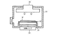
中でもランプ熱により加熱を行うランプアニール装置は量産性に優れ、高速昇温可能なことが知られており、ここに従来のランプアニール装置を図6に示す。
【0004】
処理容器11内には石英よりなる載置台12が設けられ、ガス供給管16により不活性ガスが供給されるようになっている。加熱ランプ14からの熱線は透過窓13及び載置台12を介してウエハWに照射される構造となっている。載置台12上に置かれたウエハWは、裏面側から加熱ランプ14により加熱されるが、ウエハWや載置台12を透過して処理容器11内に入射した熱線が処理容器11の内壁にて反射され、その反射された熱線も受けて加熱される。ウエハWの温度制御は熱電対等の測温計で検出した、例えばウエハ裏面の温度を加熱ランプ14のランプパワーへとフィードバックして行っている。
【0005】
【発明が解決しようとする課題】
ところで、ウエハWの面内温度均一性を確保するため、例えばウエハWの径方向の温度調整ができるように、同心円毎に発熱制御ができる加熱ランプなどを用いる工夫などがされているが、ウエハの中央部と周縁部とでは、発熱量及び放熱量のバランスにおいて程度の差が大きいため、現状では高い面内均一性の確保が困難になっている。
【0006】
例えばウエハWを昇温し、加熱処理し、降温するときのウエハWの中央部と周縁部との昇降温特性についてみると、後述する実施の形態の説明で用いている図3に示してあるように、設定されたプロセス温度でウエハ周辺部の温度が中央部より低くなっており、同一ウエハ内で温度差が生じていることが分かる。 一方、図3にもあるように従来型ランプアニール装置では、所定のプロセス温度(図3では1000℃)に致るまでの昇温時には、プロセス温度における加熱処理時とは逆にウエハ中央部の方が周縁部よりも低くなる。これは、加熱ランプからの発熱量が安定したときには、ウエハ周縁部の放熱量がどうしても大きくなってしまい、また昇温時には周縁部からの吸熱量が大きいためである。ここで今後のデバイス微細化に伴い、プロセス温度における加熱処理時は勿論のこと昇温時におけるウエハ温度の面内均一性も膜質に大きく効いてくるため、この問題を解決する方法が求められている。
【0007】
また一部の高速昇温加熱装置では、従来型ランプアニール装置で示したようなウエハ下方側の加熱ランプに加えて、ウエハ上方側にも加熱ランプを設けるものも見られるが、ウエハの温度均一性を確保することが困難であるため、例えば加熱ランプを回転させる機構などを設ける必要があり、装置が大型化、複雑化してしまうという課題があった。
【0008】
本発明は以上のような問題点に着目し、その目的は被処理基板温度の面内均一性を向上させることのできる熱処理装置を提供することにある。
【0009】
【課題を解決するための手段】
本発明は、被処理基板の載置台が設けられた処理容器と、前記載置台に載置された被処理基板を加熱処理するための加熱源と、被処理基板の温度分布を調節するために熱線の反射率を変えることができるように構成された反射部と、を備え、前記反射部は、反射面を形成する板状部と、この板状部に形成された複数の孔部と、これら孔部内に露出、没入自在に設けられ、先端面が反射面をなす可動部材と、を含み孔部内における可動部材の位置を変えることによって反射率を変えることを特徴とする熱処理装置である。
【0010】
上記の反射部は載置台と対向して設けられていることを特徴とする。
【0013】
【発明の実施の形態】
図1は本発明の熱処理方法に用いられる熱処理装置の一実施の形態を示した断面図である。21はアルミニウムよりなる処理容器であり、この処理容器21内には例えばSiCによってコーティングされたカーボン製の載置台43が設けられている。載置台43上方の処理容器21天井の壁部には例えば口径10mm程度の円筒状の孔部24が多数穿設されている。ここでウエハWに対向する処理容器21の天井部のうち、孔部24が設けられた部分を便宜的に反射部20と呼ぶことにすると、この反射部20は、例えば図2のように点線で示す多数の同心円に沿って孔部24が配置されており、最外周の同心円はウエハWより幾分大きな円をなしている。
【0014】
この夫々の孔部24内には可動部材であるピン23が電磁コイル22及び図示しないバネによって上下自在に、つまり孔部内に没入した位置と孔部が設けられていない内壁面のレベルと同じレベル位置である露出位置との間を移動自在に設けられており、制御部25から送信される信号に応じてピン23が前記孔部内を上下する。なお図2では孔部24とピン23とは便宜上共通の円で描いてある。反射部20の具体例を挙げると、例えば8インチウエハでは、7個の同心円を構成し、各同心円に沿った孔部の配列間隔は例えば15mm程度とする。ピン23の没入位置は例えば16mm程度とする。この例では処理容器21天井の壁部は反射面をなす板状部に相当する。
【0015】
前記載置台43の周囲にはウエハリフト42が設けられており、このウエハリフト42は、ウエハWの搬入出を行う図示しない搬送アームにウエハWを受け渡しすることができるように、上下する構造となっている。
【0016】
また、載置台43の上方には支持部材33により処理容器21の天井部に固定され、下方にガス噴出孔35を有するガス供給部34が載置台43と対向して設けられており、ガス供給源32とはバルブ31及びガス供給管30を介して接続されている。更に載置台43の下方には多数のガス孔を有するガス整流板44と、その更に下方側には処理容器21の下方開口部を塞ぐようにして透過窓51が下向き凸状かつ気密に取り付けられている。なお、ガス供給部34、ガス供給管30、ガス整流板44及び透過窓51は例えば石英製のものが使われる。
【0017】
前記透過窓51の内側には、N2 ガス供給源37からバルブ36及びガス供給管38を介してN2 ガスが供給されるようになっており、これは前述のガス整流板44と共に、例えば本装置をCVD等に用いる場合を考慮して設置されているものである。一方、透過窓51下方側には回転テーブル63上に同心円に沿って複数の加熱ランプ61及び反射部62が設けられ、これが一体となって加熱手段を形成している。反射部62は夫々の加熱ランプ61の側周及び底部を囲むようにした複数のすり鉢状くぼみを有した構成となっており、また加熱ランプ61は例えばハロゲンランプやアークランプが用いられる。
【0018】
次に、上述実施の形態によるウエハWの加熱処理について説明する。先ず図示しない搬送アームによりウエハWがゲートバルブ41より処理容器21内へと搬送され、ウエハリフト42に受け渡された後ウエハリフト42が降下して載置台43中央上へ載置される。処理容器21内には例えばウエハWの酸化を防ぐために、ガス供給管30及びバルブ31を介してガス供給源32から送られた不活性ガス例えばN2 ガスがガス供給部34下部にあるガス噴出孔35から供給される。
【0019】
ここで加熱ランプ61による加熱を開始する。載置台43には図示されない測温計例えば熱電対が、ウエハ裏面に接するように埋め込まれており、この熱電対により得られる検出値は図示されない伝達経路を経て制御部25へ送られ、加熱ランプ61の発光量を調節するためにフィードバックされる。そしてウエハWは所定のプロセス温度、例えば1000℃まで昇温され、その後所定のプロセス温度に所定時間維持され、しかる後降温する。
【0020】
上述の温度制御はウエハWの中央部を基準に行われるため、ウエハW中央部は図3実線のように推移する。またウエハWの周縁部は図3の点線のように推移する。ここで発明が解決しようとする課題でも述べたようにウエハWの中央部と周縁部との間に温度差が生じているため、この実施の形態では加熱ランプ61と対向する処理容器21内壁面に埋設されたピン23を上下することで夫々の箇所に反射する熱エネルギーの量を調節してウエハW表面の温度差を解消しようとしている。
【0021】
電磁コイル22はONの状態でピン23を図示しないバネの復元力に抗して孔部内に没入した形態をとるため、処理容器21内壁面に凹みができ、その箇所の熱線の反射率が小さくなる。一方電磁コイル22がOFFの状態では、バネの復元力によって処理容器21の内壁面と同レベルの位置にピン23下端が位置し、孔部をピン23が塞ぐような形態となり、熱線の反射率が先の状態よりは大きくなる。ここで電磁コイル22の制御は以下の通りに進行する。
【0022】
例えばプロセス温度を1000℃に設定すると、先ずウエハWの加熱開始時から1000℃に達するまでの昇温プロセス(図3中aで示される部分)では図4(a)の(イ)で示すようにウエハW周縁部に対向する箇所のピンが引込む(没入する)と共に図4(a)の(ロ)で示されるようにウエハW中央部に対向する箇所のピンが露出する(例えばピンの先端面が孔部以外の壁面と同じレベルになる)。従って反射部20からウエハWに放射される発熱量についてみれば、ウエハWの中央部よりも周縁部の方が小さく、このことは図2で示す温度分布を相殺する方向に作用するので、昇温時におけるウエハWの面内温度均一性が高くなる。
【0023】
この後の図3(b)で示されるt1 からt2 に致る処理プロセスでは、前述のようにウエハW周縁部の温度が中央部よりも低下するので夫々イ及びロに配置された電磁コイル22のOFF、ONが逆転し(図4(b))、ウエハW周縁部に対向する箇所のピンが露出し、中央部に対向する箇所のピンが没入し、これによりウエハW表面の温度差が相殺される。
【0024】
図3(c)で示される時間t2 経過後は装置を高速に冷却するため、加熱ランプ61への電力供給を停止するとともに図4(c)のように全てのピンを没入状態とし、反射部20の反射率を最も低い状態として降温を早めるようにする。
【0025】
上述実施の形態によれば、半導体ウエハの加熱処理において、昇温プロセス、処理プロセス及び降温プロセスの夫々に応じた温度制御を反射部20の反射率を変化させることにより行っているため、加熱開始から所定の温度における熱処理終了まで一貫して高いウエハの温度面内均一性を保つことができ、均一性の高いアニール処理を行うことができる。また加熱終了後にはウエハの冷却を高速に行うことができ、高いスループットが得られる。
【0026】
図4(a)、(b)及び(c)に示した例は、いわばオープン制御であるが、例えばクローズループで、ウエハWの表面温度に応じ露出されるピンと没入されるピンとの配列パターンを選定してもよい。またピンは露出、没入の2つの位置をとるだけでなく、没入量を調整できるように構成し、装置のセットアップの段階でピンの没入量を調整して適切な反射率を有する反射部としてもよいし、あるいはウエハの温度検出値に応じてリアルタイムで各ピンの没入量を調整するようにしてもよい。
【0027】
ここで図5は本発明に係る他の実施の形態を表したものである。この装置では加熱ランプ61等で構成される加熱手段がウエハW上方に設けられ、その加熱手段と対向するように載置台43下方側の処理容器21内壁面に反射部20が設けられる。この実施の形態では、載置台43の下面から放射される熱線を反射部20で反射し、その反射率を調整することにより載置台43の面内温度均一性を高め、以ってウエハWの面内温度均一性を高めるようにしている。
【0028】
これまで述べた実施の形態において、加熱手段に加熱ランプを用いる装置を例示したが、加熱源は加熱ランプに限定されるものではなく、例えば抵抗加熱体による加熱源を採用することも可能である。
【0029】
更に、本発明の用途は上述の加熱手段による効果を応用して例えばウエハの成膜等に利用することも可能である。
【0030】
【発明の効果】
本発明によれば、例えばウエハと対向するように反射率が可変な反射部を設けているため、ウエハ温度について高い面内均一性を維持できる。また、ウエハの加熱処理終了後には高速な放熱が為されるため、スループットが向上する。
【図面の簡単な説明】
【図1】本発明に係る一の実施の形態を表す断面図である。
【図2】図1の実施の形態で用いられる反射部を下から見た平面図である。
【図3】被処理基板中央部及び周縁部の温度変化を表した温度プロファイルである。
【図4】被処理基板の温度変化に応じて、ピンが上下する様子をあらわした反射部の断面図である。
【図5】本発明に係る他の実施の形態を表す断面図である。
【図6】従来発明に係るランプアニール装置を表す断面図である。
【符号の説明】
W ウエハ
20 反射部
21 処理容器
22 電磁コイル
23 ピン
24 孔部
25 制御部
34 ガス供給部
43 載置台
44 ガス整流板
51 透過窓
61 加熱ランプ[0001]
BACKGROUND OF THE INVENTION
The present invention relates to a heat treatment apparatus for performing heat treatment on the target substrate by, for example, heating lamp, such as a semiconductor wafer.
[0002]
[Prior art]
In the process of manufacturing a semiconductor device, for example, the step of making a semiconductor n-type or p-type is performed by thermal diffusion. As an apparatus for performing such a heat treatment, for example, an apparatus for heating a wafer using a laser or an electron beam, an apparatus using a resistance heater, an apparatus for heating by lamp heat, and the like are known.
[0003]
Among them, it is known that a lamp annealing apparatus that performs heating by lamp heat is excellent in mass productivity and can be rapidly heated, and a conventional lamp annealing apparatus is shown in FIG.
[0004]
A mounting table 12 made of quartz is provided in the
[0005]
[Problems to be solved by the invention]
By the way, in order to ensure the in-plane temperature uniformity of the wafer W, for example, a device such as a heating lamp capable of controlling heat generation for each concentric circle has been devised so that the temperature in the radial direction of the wafer W can be adjusted. Since there is a large difference in the degree of balance between the amount of heat generated and the amount of heat released between the central portion and the peripheral portion, it is difficult to ensure high in-plane uniformity at present.
[0006]
For example, the temperature rise and fall characteristics of the central portion and the peripheral portion of the wafer W when the wafer W is heated, heat-treated, and cooled are shown in FIG. 3 used in the description of the embodiment described later. Thus, it can be seen that the temperature at the peripheral portion of the wafer is lower than that at the central portion at the set process temperature, and a temperature difference occurs within the same wafer. On the other hand, in the conventional lamp annealing apparatus as shown in FIG. 3, when the temperature rises to a predetermined process temperature (1000 ° C. in FIG. 3), the central portion of the wafer is opposite to the heat treatment at the process temperature. Is lower than the periphery. This is because when the amount of heat generated from the heating lamp is stabilized, the amount of heat released from the peripheral edge of the wafer is inevitably large, and when the temperature is raised, the amount of heat absorbed from the peripheral edge is large. Here, with future device miniaturization, the in-plane uniformity of the wafer temperature at the time of temperature rise as well as the heat treatment at the process temperature has a great effect on the film quality, so a method for solving this problem is required. Yes.
[0007]
In addition to some heating lamps on the lower side of the wafer as shown in the conventional lamp annealing apparatus, some high-speed heating and heating apparatuses have a heating lamp on the upper side of the wafer. Since it is difficult to ensure the performance, for example, it is necessary to provide a mechanism for rotating the heating lamp, and there is a problem that the apparatus becomes large and complicated.
[0008]
This invention pays attention to the above problems , and the objective is to provide the heat processing apparatus which can improve the in-plane uniformity of to-be-processed substrate temperature.
[0009]
[Means for Solving the Problems]
In order to adjust the temperature distribution of a substrate to be processed, a processing container provided with a substrate for processing substrate, a heating source for heat-processing the substrate to be processed placed on the mounting table, and A reflection portion configured to change the reflectance of the heat ray, and the reflection portion includes a plate-like portion that forms a reflection surface, and a plurality of holes formed in the plate-like portion, exposed in these holes, immersive freely provided a heat treatment apparatus, characterized by changing the reflectance by changing the movable member distal end surface forms a reflecting surface, the position of the movable member in the hints hole portion.
[0010]
The reflecting portion is provided to face the mounting table.
[0013]
DETAILED DESCRIPTION OF THE INVENTION
FIG. 1 is a sectional view showing an embodiment of a heat treatment apparatus used in the heat treatment method of the present invention.
[0014]
In each
[0015]
A
[0016]
In addition, a
[0017]
Inside the
[0018]
Next, the heat treatment of the wafer W according to the above-described embodiment will be described. First, the wafer W is transferred from the gate valve 41 into the
[0019]
Here, heating by the
[0020]
Since the above temperature control is performed based on the central portion of the wafer W, the central portion of the wafer W changes as shown by a solid line in FIG. Further, the peripheral edge of the wafer W changes as indicated by the dotted line in FIG. Here, as described in the problem to be solved by the invention, a temperature difference is generated between the central portion and the peripheral portion of the wafer W. Therefore, in this embodiment, the inner wall surface of the
[0021]
Since the
[0022]
For example, when the process temperature is set to 1000 ° C., first, in the temperature raising process (the portion indicated by a in FIG. 3) from the start of heating of the wafer W to 1000 ° C., as shown in FIG. As shown in (b) of FIG. 4A, the pins at the location facing the peripheral portion of the wafer W are retracted (excluded) and the pins at the location facing the central portion of the wafer W are exposed (for example, the tip of the pin). The surface is the same level as the walls other than the holes). Accordingly, in terms of the amount of heat generated from the reflecting
[0023]
In the subsequent processing process from t1 to t2 shown in FIG. 3B, the temperature of the peripheral edge of the wafer W is lower than that in the central portion as described above, so that the
[0024]
After the elapse of time t2 shown in FIG. 3 (c), the power supply to the
[0025]
According to the above-described embodiment, in the heat treatment of the semiconductor wafer, since the temperature control corresponding to each of the temperature raising process, the treatment process, and the temperature lowering process is performed by changing the reflectance of the
[0026]
The examples shown in FIGS. 4A, 4 </ b> B, and 4 </ b> C are so-called open control. For example, in a closed loop, an arrangement pattern of pins that are exposed and immersed according to the surface temperature of the wafer W is shown. You may choose. Also, the pin can be adjusted not only in two positions, exposure and immersion, but also in the amount of immersion, and as a reflection part with appropriate reflectivity by adjusting the pin immersion amount at the stage of device setup Alternatively, the immersion amount of each pin may be adjusted in real time according to the detected temperature value of the wafer.
[0027]
FIG. 5 shows another embodiment according to the present invention. In this apparatus, a heating unit composed of a
[0028]
In the embodiments described so far, the apparatus using the heating lamp as the heating means has been exemplified. However, the heating source is not limited to the heating lamp, and for example, a heating source using a resistance heating body can be adopted. .
[0029]
Furthermore, the application of the present invention can be applied to, for example, film formation of a wafer by applying the effect of the heating means described above.
[0030]
【The invention's effect】
According to the present invention, for example, since the reflective portion having a variable reflectance is provided so as to face the wafer, high in-plane uniformity can be maintained with respect to the wafer temperature. In addition, after heat treatment of the wafer is completed, high-speed heat dissipation is performed, so that throughput is improved.
[Brief description of the drawings]
FIG. 1 is a cross-sectional view showing an embodiment according to the present invention.
FIG. 2 is a plan view of a reflection part used in the embodiment of FIG. 1 as viewed from below.
FIG. 3 is a temperature profile showing a temperature change in a central portion and a peripheral portion of a substrate to be processed.
FIG. 4 is a cross-sectional view of a reflecting portion showing how pins move up and down according to a temperature change of a substrate to be processed.
FIG. 5 is a sectional view showing another embodiment according to the present invention.
FIG. 6 is a cross-sectional view showing a lamp annealing apparatus according to a conventional invention.
[Explanation of symbols]
Claims (2)
前記反射部は、反射面を形成する板状部と、この板状部に形成された複数の孔部と、これら孔部内に露出、没入自在に設けられ、先端面が反射面をなす可動部材と、を含み、孔部内における可動部材の位置を変えることによって反射率を変えることを特徴とする熱処理装置。 A processing container provided with a mounting table for the substrate to be processed, a heating source for heat-treating the processing substrate mounted on the mounting table, and a heat ray reflectance to adjust the temperature distribution of the substrate to be processed and a reflecting portion configured to be able to change the,
The reflection portion includes a plate-like portion that forms a reflection surface, a plurality of holes formed in the plate-like portion, and a movable member that is exposed and immersible in the holes and the tip surface forms a reflection surface. And the reflectance is changed by changing the position of the movable member in the hole.
Priority Applications (1)
| Application Number | Priority Date | Filing Date | Title |
|---|---|---|---|
| JP07621199A JP4409655B2 (en) | 1999-03-19 | 1999-03-19 | Heat treatment equipment |
Applications Claiming Priority (1)
| Application Number | Priority Date | Filing Date | Title |
|---|---|---|---|
| JP07621199A JP4409655B2 (en) | 1999-03-19 | 1999-03-19 | Heat treatment equipment |
Publications (2)
| Publication Number | Publication Date |
|---|---|
| JP2000269155A JP2000269155A (en) | 2000-09-29 |
| JP4409655B2 true JP4409655B2 (en) | 2010-02-03 |
Family
ID=13598851
Family Applications (1)
| Application Number | Title | Priority Date | Filing Date |
|---|---|---|---|
| JP07621199A Expired - Fee Related JP4409655B2 (en) | 1999-03-19 | 1999-03-19 | Heat treatment equipment |
Country Status (1)
| Country | Link |
|---|---|
| JP (1) | JP4409655B2 (en) |
Families Citing this family (6)
| Publication number | Priority date | Publication date | Assignee | Title |
|---|---|---|---|---|
| JP4896555B2 (en) * | 2006-03-29 | 2012-03-14 | 株式会社東芝 | Semiconductor manufacturing apparatus and semiconductor device manufacturing method |
| KR101324211B1 (en) * | 2006-05-29 | 2013-11-06 | 주성엔지니어링(주) | Substrate processing apparatus |
| US8796777B2 (en) | 2009-09-02 | 2014-08-05 | Qualcomm Incorporated | Fin-type device system and method |
| US8986454B2 (en) * | 2010-06-08 | 2015-03-24 | Applied Materials, Inc. | Window assembly for use in substrate processing systems |
| KR101324210B1 (en) * | 2012-10-10 | 2013-11-06 | 주성엔지니어링(주) | Substrate processing apparatus |
| CN118486609B (en) * | 2024-05-28 | 2025-04-01 | 扬州思普尔科技有限公司 | A semiconductor wafer annealing furnace based on a new chamber structure |
-
1999
- 1999-03-19 JP JP07621199A patent/JP4409655B2/en not_active Expired - Fee Related
Also Published As
| Publication number | Publication date |
|---|---|
| JP2000269155A (en) | 2000-09-29 |
Similar Documents
| Publication | Publication Date | Title |
|---|---|---|
| JP5518043B2 (en) | Temperature measurement and control of wafer support in heat treatment chamber | |
| KR102504970B1 (en) | Substrate support device, thermal processing apparatus, substrate support method, and thermal processing method | |
| KR100976649B1 (en) | Controlled Annealing Method | |
| US6963692B2 (en) | Heat-treating methods and systems | |
| KR101724423B1 (en) | Apparatus and method for enhancing the cool down of radiatively heated substrates | |
| KR20130087530A (en) | Transparent reflector plate for rapid thermal processing chamber | |
| WO2005029561A1 (en) | Heat treatment apparatus | |
| JP2013093600A (en) | Back side rapid thermal processing of patterned wafers | |
| US11164761B2 (en) | Heat treatment method and heat treatment apparatus of light irradiation type | |
| US11289344B2 (en) | Heat treatment method and heat treatment apparatus for managing dummy wafer | |
| US10998207B2 (en) | Heat treatment method and heat treatment apparatus for managing heat treatment of dummy wafer | |
| US20170110347A1 (en) | Substrate supporting unit, substrate processing apparatus, and method of manufacturing substrate supporting unit | |
| JP4409655B2 (en) | Heat treatment equipment | |
| JP2010129861A (en) | Thermal processing apparatus | |
| TWI738120B (en) | Heat treatment method and heat treatment apparatus | |
| JP2009027001A (en) | Light irradiation type heat treatment equipment | |
| TWI761218B (en) | Heat treatment apparatus | |
| JP5169055B2 (en) | Semiconductor wafer heat treatment equipment | |
| JP2002289548A (en) | Heat treatment device | |
| TW202030802A (en) | Heat treatment method and heat treatment apparatus | |
| JP3709359B2 (en) | Substrate heat treatment equipment | |
| JP2025531068A (en) | Reflector plate for substrate processing | |
| KR20200021818A (en) | Hot plate and apparatus for heat-treating substrate with the hot plate, and fabricating method of the hot plate |
Legal Events
| Date | Code | Title | Description |
|---|---|---|---|
| A621 | Written request for application examination |
Free format text: JAPANESE INTERMEDIATE CODE: A621 Effective date: 20051118 |
|
| A977 | Report on retrieval |
Free format text: JAPANESE INTERMEDIATE CODE: A971007 Effective date: 20090521 |
|
| A131 | Notification of reasons for refusal |
Free format text: JAPANESE INTERMEDIATE CODE: A131 Effective date: 20090609 |
|
| A521 | Written amendment |
Free format text: JAPANESE INTERMEDIATE CODE: A523 Effective date: 20090810 |
|
| TRDD | Decision of grant or rejection written | ||
| A01 | Written decision to grant a patent or to grant a registration (utility model) |
Free format text: JAPANESE INTERMEDIATE CODE: A01 Effective date: 20091027 |
|
| A01 | Written decision to grant a patent or to grant a registration (utility model) |
Free format text: JAPANESE INTERMEDIATE CODE: A01 |
|
| A61 | First payment of annual fees (during grant procedure) |
Free format text: JAPANESE INTERMEDIATE CODE: A61 Effective date: 20091112 |
|
| R150 | Certificate of patent or registration of utility model |
Free format text: JAPANESE INTERMEDIATE CODE: R150 |
|
| FPAY | Renewal fee payment (event date is renewal date of database) |
Free format text: PAYMENT UNTIL: 20121120 Year of fee payment: 3 |
|
| LAPS | Cancellation because of no payment of annual fees |