JP4368498B2 - Semiconductor device, semiconductor wafer and manufacturing method thereof - Google Patents
Semiconductor device, semiconductor wafer and manufacturing method thereof Download PDFInfo
- Publication number
- JP4368498B2 JP4368498B2 JP2000143725A JP2000143725A JP4368498B2 JP 4368498 B2 JP4368498 B2 JP 4368498B2 JP 2000143725 A JP2000143725 A JP 2000143725A JP 2000143725 A JP2000143725 A JP 2000143725A JP 4368498 B2 JP4368498 B2 JP 4368498B2
- Authority
- JP
- Japan
- Prior art keywords
- insulating layer
- forming
- semiconductor device
- film
- multilayer
- Prior art date
- Legal status (The legal status is an assumption and is not a legal conclusion. Google has not performed a legal analysis and makes no representation as to the accuracy of the status listed.)
- Expired - Lifetime
Links
Images


Classifications
-
- H10W20/069—
-
- H10P14/662—
-
- H10P14/69215—
-
- H10P14/6925—
-
- H10W20/071—
-
- H10W20/074—
-
- H10W20/075—
-
- H10W20/097—
-
- H10W20/48—
-
- H10P14/6336—
-
- H10P14/6342—
-
- H10P14/665—
-
- H10P14/6682—
-
- H10P14/6686—
-
- H10P14/6922—
-
- H10P14/6926—
Landscapes
- Internal Circuitry In Semiconductor Integrated Circuit Devices (AREA)
- Formation Of Insulating Films (AREA)
- Chemical Vapour Deposition (AREA)
Description
【0001】
【発明の属する技術分野】
本発明は、低誘電率膜の形成された半導体ウェーハ、低誘電率膜中に配線等の形成された半導体装置、およびこれらの製造方法に関する。
【0002】
【従来の技術】
近年、素子の高速動作性に対する要請から、配線間容量を小さくする低誘電率材料を利用する技術が、盛んに検討されている。
【0003】
以下、図6〜7を参照して、低誘電率材料を用いたダマシン銅配線の形成プロセスについて説明する。
【0004】
まず図6(a)のように、シリコン基板上に形成された下層配線層(不図示)の上にシリコン窒化膜1を成膜した後、この上にMSQ(Methyl Silsesquioxane メチルシルセスキオキサン)膜2を成膜する。MSQ膜2の成膜は、回転塗布法等により行う。次いでこの上に酸化シリコンからなるシリコン酸化膜4を成膜する。シリコン酸化膜4は、次工程で用いるレジストを剥離する際の酸素プラズマアッシングに対する耐性を高め、また、吸湿による誘電率上昇を防止する等の目的で形成される。つづいて、シリコン酸化膜4の上に不図示のレジストマスクを形成した後、ドライエッチングにより、MSQ膜2およびシリコン酸化膜4中に、シリコン窒化膜1に達する配線溝を形成する(図6(c))。
【0005】
次にスパッタリング法等により、全面にバリアメタル膜5を形成する(図7(a))。次に全面に銅膜6を形成した後、CMPによる平坦化を行い、配線溝内に銅膜6を残してダマシン配線を完成する(図7(b))。
【0006】
以上の手順により得られる半導体装置は、配線間が低誘電率のMSQ膜2によって充填されているため、クロストークを有効に防止できる。ところが、有機材料からなるMSQ膜2の上に無機材料からなるシリコン酸化膜4が形成されているため、これらの膜の界面の密着性が悪く、後工程で図5のように剥離が発生しやすい。低誘電率を得るためにはMSQ膜2の有機成分を増加させるのが有利であり、一方、シリコン酸化膜4についてはアッシング耐性等の要請から無機材料とすることが望ましい。このため、これらの膜の親和性が不良となり、界面で剥離が発生しやすくなるのである。このような剥離が生じると、配線工程における歩留まり低下の原因となる。
【0007】
このような剥離を防止するため、MSQ膜2に代えて有機成分を含まないHSQ(Hydrogen Silisesquioxane ハイドロジェンシルセスキオキサン)等の材料を用いることも考えられるが、この場合、MSQを用いた場合に比較して誘電率が上昇する。
【0008】
また、剥離防止のため、MSQ膜成膜後、その表面に対してオゾン処理、UV−オゾン処理または酸素プラズマ処理等を行い、密着性を向上させることも検討されてきた。しかし、これらの方法では、膜中に水分が侵入したり絶縁膜の誘電率が上昇する上、膜の表面が荒れて残渣が生じるといった問題が発生する。そこで、このような問題の生じない、密着性向上手段が望まれていた。
【0009】
一方、微細加工技術に対する要求水準が高まる中、層間絶縁膜形成後の平坦化プロセスの重要性が益々高まりつつある。良好な平坦度が得られないと、露光の焦点がずれ、フォトレジストの加工が困難になるだけでなく、そのフォトレジストをマスクにした後のエッチング工程でのエッチング残りが多発することになる。層間絶縁膜の平坦性を高めるため、従来、メタル配線工程の前工程の絶縁膜材料として、リフロー性を有するBPSG(リンボロンガラス)等が用いられてきた。以下、図8〜9を参照して、BPSGを用いた従来のメモリ系デバイスの形成プロセスについて説明する。
【0010】
まず図8(a)に示すように、シリコン半導体基板上にワード線を兼ねるゲート電極60を形成する。以下、この状態に至るまでの工程の概略を説明する。はじめにp-形シリコン単結晶からなる半導体基板51の表面に選択酸化によりフィールド絶縁膜53を形成する。次にリンをイオン注入し、p型ウエル領域52を形成する。つづいて熱酸化処理により酸化シリコン膜61を形成した後、その上に多結晶シリコン膜62、WSi膜63、シリコン窒化膜64を成膜する。次いでこれらの膜をエッチングによりパターニングしてゲート電極60を形成する。つづいてシリコン窒化膜を成膜後、異方性エッチングを行い、ゲート電極60側面に窒化シリコンからなる側壁絶縁膜65を形成する。つづいて、イオン注入を行うことにより不純物拡散層54を形成する。以上の工程により図8(a)の状態となる。
【0011】
次にCVD法により、BPSG膜55を成膜する。成膜後、窒素アニールによるリフローを行う。その後、バッファードフッ化水素(BHF)を用いてエッチバックを行い、BPSG膜55表面を平坦化する(図8(b))。
【0012】
次に、BPSG膜55の表面にパターニングされたフォトレジスト(不図示)を設けた後、これをマスクとしてBPSG膜55をドライエッチングにより加工し、コンタクトホール57を形成する(図9(a))。このとき側壁絶縁膜65がエッチング阻止膜として機能し、接続孔57がセルフアラインに形成される。次いでバッファードフッ酸を用いて不純物拡散層54上の自然酸化膜を除去する。
【0013】
その後、接続孔57を埋め込むように多結晶シリコン膜72を形成した後、リンを添加する。さらにタングステンシリサイド(WSi)膜73およびシリコン酸化膜74を堆積した後、エッチングによりビット線を形成する(図9(b))。
【0014】
ところが、近年においては高集積化の要請からゲート電極(ワード線)の間隔が0.2μm以下ときわめて狭くなっているため、層間絶縁膜材料として、優れたギャップフィル性が求められる。特に、上記したプロセスのように、ゲート電極の側壁絶縁膜によりコンタクト孔と配線層の間の絶縁を確保する、いわゆるセルフアラインーコンタクト技術の採用が必須となるような高集積化プロセスにおいては、絶縁材料の埋め込み性に対する要求水準もきわめて高いものとなる。絶縁膜材料としてBPSGを用いる従来技術では、かかる要求に応えることは困難であり、よりギャップフィル性の優れる材料を用いることが必須となる。このような要求を満たす絶縁膜として、HSQ等の無機SOG膜や、MSQ等の有機SOG膜が考えられる。ところが、HSQは薬液耐性が低いため、バッファードフッ酸による自然酸化膜を除去工程でサイドエッチングが進行し、設計通りの形状のコンタクトホールを形成することが困難となる。また、HSQ以外の無機SOG膜は、一般にクラックが発生しやすいという問題がある。以上のことから、MSQ等の有機SOG膜が、最も好適に用いられる。MSQ等の有機低誘電率膜は、狭いギャップに対する埋め込み性に優れ、しかも良好な平坦性が得られる。
【0015】
ところが、MSQ等の有機低誘電率材料を用いた場合、アッシング耐性等を付与するため、その上に酸化シリコン等からなる無機保護膜を形成することが必要となる。この結果、前述したようにMSQ膜と無機保護膜との間の剥離の発生が問題となる。
【0016】
【発明が解決しようとする課題】
本発明は、上記事情に鑑み、有機低誘電率材料の持つ優れた誘電特性、平坦性およびギャップフィル特性を損なうことなく、低誘電率膜と保護膜との界面密着性を改善することを目的とする。
【0017】
【課題を解決するための手段】
上記課題を解決する本発明は、以下の事項により特定される。
【0018】
[1]半導体基板上に多層絶縁膜が設けられ、該多層絶縁膜中に配線が形成された半導体装置であって、該多層絶縁膜は、酸化シリコンよりも低い誘電率を有する有機低誘電率材料からなる第一の絶縁層と、該第一の絶縁層の上部に接して形成されたSi−H基を有するポリシロキサン化合物からなる第二の絶縁層と、該第二の絶縁層の上部に接して形成された無機材料からなる第三の絶縁層と、を含んでなることを特徴とする半導体装置。
【0019】
[2][1]に記載の半導体装置であって、前記第一の絶縁層は、オルガノポリシロキサンまたは芳香族含有有機樹脂からなることを特徴とする半導体装置。
【0020】
[3][1]または[2]に記載の半導体装置であって、前記第二の絶縁層は、ハイドロジェンシルセスキオキサンおよび/またはヒドリドオルガノシロキサンであることを特徴とする半導体装置。
【0021】
[4][1]乃至[3]いずれかに記載の半導体装置であって、前記第三の絶縁層は、酸化シリコン、窒化シリコンおよび酸窒化シリコンからなる群から選ばれる一または二以上の材料からなることを特徴とする半導体装置。
【0022】
[5]一表面に多層絶縁膜が形成された半導体ウェーハであって、該多層絶縁膜は、酸化シリコンよりも低い誘電率を有する有機低誘電率材料からなる第一の絶縁層と、該第一の絶縁層の上部に接して形成されたSi−H基を有するポリシロキサン化合物からなる第二の絶縁層と、該第二の絶縁層の上部に接して形成された無機材料からなる第三の絶縁層と、を含んでなることを特徴とする半導体ウェーハ。
【0023】
[6][5]に記載の半導体ウェーハであって、前記第一の絶縁層は、オルガノポリシロキサンまたは芳香族含有有機樹脂からなることを特徴とする半導体ウェーハ。
【0024】
[7][5]または[6]に記載の半導体ウェーハであって、前記第二の絶縁層は、ハイドロジェンシルセスキオキサンおよび/またはヒドリドオルガノシロキサンであることを特徴とする半導体ウェーハ。
【0025】
[8][5]乃至[7]いずれかに記載の半導体ウェーハであって、前記第三の絶縁層は、酸化シリコン、窒化シリコンおよび酸窒化シリコンからなる群から選ばれる一または二以上の材料からなることを特徴とする半導体ウェーハ。
【0026】
[9]半導体ウェーハ上に第一の絶縁層、第二の絶縁層および第三の絶縁層を含む多層絶縁膜を形成する方法であって、酸化シリコンよりも低い誘電率を有する有機低誘電率材料からなる第一の絶縁層を形成する工程と、第一の絶縁層の上部に接するように、Si−H基を有するポリシロキサン化合物からなる第二の絶縁層を形成する工程と、第二の絶縁層の上部に接するように、無機材料からなる第三の絶縁層を形成する工程と、を有することを特徴とする多層絶縁膜の形成方法。
【0027】
[10][9]に記載の多層絶縁膜の形成方法であって、前記第一の絶縁層は、オルガノポリシロキサンまたは芳香族含有有機樹脂からなることを特徴とする多層絶縁膜の形成方法。
【0028】
[11][9]または[10]に記載の多層絶縁膜の形成方法であって、前記第二の絶縁層は、ハイドロジェンシルセスキオキサンおよび/またはヒドリドオルガノシロキサンであることを特徴とする多層絶縁膜の形成方法。
【0029】
[12][9]乃至[11]いずれかに記載の多層絶縁膜の形成方法であって、前記第三の絶縁層は、酸化シリコン、窒化シリコンおよび酸窒化シリコンからなる群から選ばれる一または二以上の材料からなることを特徴とする多層絶縁膜の形成方法。
【0030】
[13][9]乃至[12]いずれかに記載の多層絶縁膜の形成方法であって、プラズマCVD法を用い、プラズマ雰囲気から半導体ウェーハを取り出すことなく、前記第一の絶縁層および前記第二の絶縁層を形成することを特徴とする多層絶縁膜の形成方法。
【0031】
[14][13]に記載の多層絶縁膜の形成方法であって、前記第一の絶縁層の形成に用いる原料ガスを、アルキルシランガスおよび酸化性ガスを含む混合ガスとし、第二の絶縁層の形成に用いる原料ガスを、モノシランガス、アルキルシランガスおよび酸化性ガスを含む混合ガスとすることを特徴とする多層絶縁膜の形成方法。
【0032】
[15][9]乃至[12]いずれかに記載の多層絶縁膜の形成方法であって、半導体ウェーハ上に前記有機低誘電率材料を含む溶液を回転塗布した後、熱処理を行うことにより第一の絶縁層を形成し、次いで200℃以上500℃以下の雰囲気下で加熱処理を行い、その後、プラズマCVD法を用いて第二の絶縁層を形成することを特徴とする多層絶縁膜の形成方法。
【0033】
[16]半導体基板上に、酸化シリコンよりも低い誘電率を有する有機低誘電率材料からなる第一の絶縁層を形成する工程と、第一の絶縁層の上部に接するように、Si−H基を有するポリシロキサン化合物からなる第二の絶縁層を形成する工程と、第二の絶縁層の上部に接するように、無機材料からなる第三の絶縁層を形成する工程と、第一の絶縁層、第二の絶縁層および第三の絶縁層をエッチングして凹部を形成する工程と、該凹部を埋め込むように全面に導電膜を形成する工程と、化学的機械的研磨またはエッチングにより、凹部外の領域に形成された導電膜を除去する工程と、を有することを特徴とする半導体装置の製造方法。
【0034】
[17]半導体基板上に、側面に側壁絶縁膜が設けられたゲート電極を形成し、該ゲート電極の両側の半導体基板表面領域に一対の不純物拡散領域を形成する工程と、全面に酸化シリコンよりも低い誘電率を有する有機低誘電率材料からなる第一の絶縁層を形成する工程と、第一の絶縁層の上部に接するように、Si−H基を有するポリシロキサン化合物からなる第二の絶縁層を形成する工程と、第二の絶縁層の上部に接するように、無機材料からなる第三の絶縁層を形成する工程と、第一の絶縁層、第二の絶縁層および第三の絶縁層をエッチングして接続孔を設け、該接続孔の底部に前記不純物拡散領域を露出させるとともに該接続孔の側面に前記側壁絶縁膜を露出させる工程と、該接続孔を埋め込むように全面に導電膜を形成する工程と、を有することを特徴とする半導体装置の製造方法。
【0035】
[18][16]または[17]に記載の半導体装置の製造方法であって、前記第一の絶縁層は、オルガノポリシロキサンまたは芳香族含有有機樹脂からなることを特徴とする半導体装置の製造方法。
【0036】
[19][16]乃至[18]いずれかに記載の半導体装置の製造方法であって、前記第二の絶縁層は、ハイドロジェンシルセスキオキサンおよび/またはヒドリドオルガノシロキサンであることを特徴とする半導体装置の製造方法。
【0037】
[20][16]乃至[19]いずれかに記載の半導体装置の製造方法であって、前記第三の絶縁層は、酸化シリコン、窒化シリコンおよび酸窒化シリコンからなる群から選ばれる一または二以上の材料からなることを特徴とする半導体装置の製造方法。
【0038】
[21][16]乃至[20]いずれかに記載の半導体装置の製造方法であって、プラズマCVD法を用い、プラズマ雰囲気から半導体ウェーハを取り出すことなく、前記第一の絶縁層および前記第二の絶縁層を形成することを特徴とする半導体装置の製造方法。
【0039】
[22][21]に記載の半導体装置の製造方法であって、前記第一の絶縁層の形成に用いる原料ガスを、アルキルシランガスおよび酸化性ガスを含む混合ガスとし、第二の絶縁層の形成に用いる原料ガスを、モノシランガス、アルキルシランガスおよび酸化性ガスを含む混合ガスとすることを特徴とする半導体装置の製造方法。
【0040】
[23][16]乃至[20]いずれかに記載の半導体装置の製造方法であって、半導体ウェーハ上に前記有機低誘電率材料を含む溶液を回転塗布した後、熱処理を行うことにより第一の絶縁層を形成し、次いで200℃以上500℃以下の雰囲気下で加熱処理を行い、その後、プラズマCVD法を用いて第二の絶縁層を形成することを特徴とする半導体装置の製造方法。
【0041】
上記本発明によれば、第一の絶縁層として有機低誘電率材料を用いているため、配線間のクロストークを防止でき、また、狭いギャップを絶縁膜材料により好適に埋め込むことができる。そして、第一の絶縁層と第三の絶縁層との間に、Si−H基を有するポリシロキサン化合物からなる第二の絶縁層を介在させているため、層間密着性が良好となり、各層の界面剥離を効果的に防止することができる。このため、プロセスの歩留まりを向上できるとともに、信頼性の高い半導体装置を得ることができる。
【0042】
なお、[16]記載の発明における凹部とは、配線溝、接続孔等、任意の形状のものを含む。また、[17]記載の発明においては、不純物拡散領域を形成するためのイオン注入は、ゲート電極パターン形成後に行われるが、側壁絶縁膜形成前後のいずれの段階で行っても良い。
【0043】
【発明の実施の形態】
本発明における第一の絶縁層は、酸化シリコンよりも低い誘電率を有する有機低誘電率材料からなる。好ましくは比誘電率3.5以下、より好ましくは比誘電率3.0以下のものが用いられ、たとえば、オルガノポリシロキサンまたは芳香族含有有機樹脂が好ましく用いられる。
【0044】
オルガノポリシロキサンとは、有機官能基を有するポリシロキサンであり、誘電特性および加工性に優れることから、アルキルシルセスキオキサンやヒドリドアルキルシロキサン等が好ましく用いられる。たとえば下記繰り返し単位(I)および(III)からなるメチルシルセスキオキサン、または、繰り返し単位(I)、(II)および(III)等からなるメチル化ハイドロジェンシルセスキオキサン(以下、適宜、「MHSQ」という。)が好ましく用いられ、このうち、誘電特性および加工性がより優れるメチルシルセスキオキサンが特に好ましく用いられる。
【0045】
【化1】
なお、MHSQを用いる場合、(I)、(II)および(III)の合計に対する(I)のモル比は、好ましくは0.5以上、より好ましくは0.7以上とする。(I)の含有率が低すぎると誘電率を充分に低くすることが困難であり、また、加工性が損なわれる場合がある。
【0047】
芳香族含有有機樹脂としては、ポリアリールエーテル(PAE)、ジビニルシロキサン−ビス−ベンゾシクロブテン(BCB)等を例示することができる。これらは、比誘電率が低い上、耐熱性も比較的良好である。
【0048】
本発明における第二の絶縁層は、Si−H基を有するポリシロキサン化合物からなる。たとえば上記した繰り返し単位(II)および(III)からなるハイドロジェンシルセスキオキサン、または、繰り返し単位(I)、(II)および(III)等からなるMHSQが好ましく用いられる。これらのポリマーは、分子中にSi−H基を有するため、有機低誘電率絶縁膜からなる第一の絶縁層、および、無機材料からなる第三の絶縁層との密着性に優れる。これらの層との密着性に優れる理由は必ずしも明らかではないが、Si−Hが脱水素化して反応活性部位が形成され、第一および第三の絶縁層の構成材料と反応を起こすことによるものと推察される。
【0049】
なお、MHSQを用いる場合、(I)、(II)および(III)の合計に対する(II)のモル比は、好ましくは0.2以上、より好ましくは0.5以上とする。このような範囲とすることで、より充分な層間密着性を得ることができる。
【0050】
本発明における第三の絶縁層は、レジストを剥離する際の酸素プラズマアッシングに対する耐性を高め、CMPを行う際のスクラッチ耐性を高め、また、吸湿による誘電率上昇を防止する等の目的で形成される。第三の絶縁層は、たとえば、酸化シリコン、窒化シリコンおよび酸窒化シリコンからなる群から選ばれる一または二以上の材料からなるものとすることが好ましい。
【0051】
本発明における多層絶縁膜は、上記した第一、第二および第三の絶縁層を含んでなるが、これらの層のうち、第一の絶縁層が最も最も厚いことが好ましい。本発明は、第一の絶縁層を構成する有機低誘電率材料の優れた誘電特性、平坦性およびギャップフィル特性を有効活用するものだからである。なお、本発明における多層絶縁膜において、第二の絶縁層中に、MSQ等からなる他の材料層が挿入されていてもよい。
【0052】
本発明における第一の絶縁層は、プラズマCVD法、スピンコート法等により形成することができる。プラズマCVD法による場合は、原料ガスとして、アルキルシランガスおよび酸化性ガスの混合ガスを用いる。アルキルシランガスとしては、モノメチルシラン、ジメチルシラン、トリメチルシランまたはテトラメチルシラン等が挙げられ、これらを単独で使用、または2種以上を併用することができる。このうち、トリメチルシランが好適に用いられる。
酸化性ガスとは、アルキルシランに対する酸化作用を示すガスであって、分子中に酸素元素を含むものが用いられる。たとえば、NO、NO2、CO、CO2およびO2からなる群から選ばれる一または二以上のガスを用いることができ、このうち、酸化力の強さが適度であることから、NOおよびNO2が好ましく用いられる。一方、第一の絶縁層をスピンコート法により形成する場合は、所定の回転速度で回転するウェーハ上に層材料の溶解した溶液を滴下して塗布し、次いで多段階の熱処理を行って乾燥、固化を行うことにより成膜する。
【0053】
本発明における第二の絶縁層は、第一の絶縁層と同様、プラズマCVD法、スピンコート法等により形成することができる。より高度の密着性が必要となる場合は、プラズマCVD法を用いることが好ましい。
【0054】
プラズマCVD法による場合は、原料ガスとしては、モノシラン(SiH4)ガス、アルキルシランガスおよび酸化性ガスの混合ガスを用いることが好ましい。アルキルシランガスとしては、モノメチルシラン、ジメチルシラン、トリメチルシランまたはテトラメチルシラン等が挙げられ、これらを単独で使用、または2種以上を併用することができる。このうちトリメチルシランが好適に用いられる。酸化性ガスとは、アルキルシランに対する酸化作用を示すガスであって、分子中に酸素元素を含むものが用いられる。たとえば、NO、NO2、CO、CO2およびO2からなる群から選ばれる一または二以上のガスを用いることができ、このうち、酸化力の強さが適度であることから、NOおよびNO2が好ましく用いられる。
【0055】
一方、第一の絶縁層をスピンコート法により形成する場合は、所定の回転速度で回転するウェーハ上に層材料の溶解した溶液を滴下して塗布し、次いで多段階の熱処理を行って乾燥、固化を行うことにより成膜する。
【0056】
本発明における第三の絶縁層は、熱CVD法やプラズマCVD法により形成することができる。原料ガスとしては、たとえば、モノシラン(SiH4)ガスおよび酸化性ガスの混合ガス、あるいは、テトラエトキシシラン(TEOS)等を用いることができる。
【0057】
本発明においては、上記第一および第二の絶縁層の形成を、下記(i)または(ii)の方法により行うことが好ましい。
(i)プラズマCVD法を用い、プラズマ雰囲気から半導体ウェーハを取り出すことなく第一の絶縁層、第二の絶縁層を形成する方法。
(ii)半導体ウェーハ上に前記有機低誘電率材料を含む溶液を回転塗布した後、熱処理を行うことにより第一の絶縁層を形成し、次いで200℃以上500℃以下、好ましくは350℃以上500℃以下の雰囲気下で加熱処理を行い、その後、第二の絶縁層を形成する方法。
【0058】
上記(i)の方法では、プラズマ雰囲気から半導体ウェーハを取り出すことがないため、第二の絶縁層に含まれるSi−H基の反応性が低下することを防止でき、また、形成された層の吸湿を防止でき、この結果、第二の絶縁層と他の層との密着性が特に良好となる。
【0059】
上記(ii)の方法では、第一の絶縁層を回転塗布法により形成するため、狭いギャップ間にも確実に絶縁材料を形成することができる。このため、従来技術の項で説明したゲート電極上の層間絶縁膜形成プロセス(図8)等に好適に適用することができる。また、この方法では、第一の絶縁層を形成後、所定の温度で加熱処理を行うため、第一の絶縁層と第二の絶縁層との間の密着性が更に良好となる。この理由は必ずしも明らかでないが、第一の絶縁層表面に吸着した水等が揮発すること、第一の絶縁層表面の活性が高まること等により、第二の絶縁層の構成材料との反応がより円滑に進行するためと考えられる。なお、この熱処理は、減圧下、たとえば1〜100Paの雰囲気で行うことが好ましく、処理時間は、通常、1〜10分程度とする。
【0060】
本発明において、「配線」とは、トランジスタ等の素子を電気的に接続するものの総称として用いており、メモリ素子におけるゲート電極を兼ねるワード線等も含む。本発明は、多層絶縁膜に設けられた複数の凹部に導電膜が埋め込まれてなるダマシン配線構造や、ゲート電極上にセルフアラインコンタクトを設ける構造に適用した場合、特に効果的である。
【0061】
【実施例】
実施例1
本実施例では、ダマシン銅配線が積層されてなる多層配線構造を備えた半導体装置を作製する際のプロセスの一例を示す。
【0062】
ロジック系デバイス等においては、図4のように複数の配線層が積層された多層配線構造がしばしば採用される。シリコン基板40上の第一層(素子形成層)にゲート電極42および不純物拡散層41からなるトランジスタが形成され、その上に、層間絶縁膜45中に設けられた銅配線44が多層に積層した構造となっている。各銅配線間は層間接続プラグ43により接続されている。
【0063】
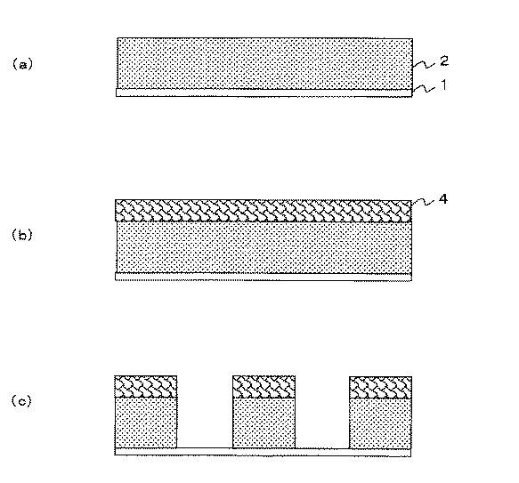
本実施例では、このような多層配線を構成する各配線層の詳細な構造を図1のようにした。図1に示す配線構造は、シリコン窒化膜1上に、MSQ(メチルシルセスキオキサン)膜2、MHSQ(メチル化ハイドロジェンシルセスキオキサン)膜3、およびシリコン酸化膜4がこの順で積層された多層絶縁膜が形成されている。この多層絶縁膜中に、複数の配線溝が形成され、その内部にTaからなるバリアメタル膜5を介して銅膜6が埋め込まれた構造となっている。銅膜6の厚みは200〜500nm程度である。
【0064】
以下、図1の配線構造を形成するプロセスについて図面を参照して説明する。まず図2(a)のように、下層配線層(不図示)の上にプラズマCVD法によりシリコン窒化膜1(膜厚50nm)を成膜した後、この上にMSQ膜2(膜厚250nm)を成膜した。MSQ膜2成膜時の原料ガスは、トリメチルシランおよびN2Oの混合ガスを用いた。MSQ膜2は、下記繰り返し単位(I)および(III)からなる構造を有する。
【0065】
【化2】
MSQ膜2の成膜後、その上にプラズマCVD法によりMHSQ膜3(膜厚50nm)を形成した(図2(b))。原料ガスは、モノシラン(SiH4)、トリメチルシランおよびN2Oの混合ガスを用いた。MHSQ膜3は、上記繰り返し単位(I)、(II)および(III)からなる構造を有する。原料ガスの組成比から、(I)、(II)および(III)の合計に対する(II)のモル比は、0.5〜0.6である。
【0067】
つづいてMHSQ膜3上にプラズマCVD法等によりシリコン酸化膜4(膜厚100nm)を形成した(図2(c))。原料ガスとしては、モノシラン(SiH4)およびN2Oの混合ガスを用いた。
【0068】
以上のようにして、MSQ膜2、MHSQ膜3およびシリコン酸化膜4が積層してなる多層膜を形成した。これらは、プラズマ装置内のプラズマ雰囲気からウェーハを取り出すことなく、原料ガスを変えて一連の工程で成膜を行った。その後、この多層膜をドライエッチングし、シリコン窒化膜1に達する配線溝を形成した(図2(d))。
【0069】
つづいて、スパッタリング法により、全面にTaからなるバリアメタル膜5を形成した(図3(a))。次にめっき法により、全面に銅膜6を形成した(図3(b))。銅膜6の形成はCVD法やスパッタリング法等により行うこともできるが、カバレッジの良好なめっき法またはCVD法によることが好ましい。銅膜6形成後、全面をCMPにより平坦化し、配線溝内に銅膜6を残してダマシン配線を完成した。
【0070】
以上のプロセスにより得られた半導体装置は、配線間が低誘電率のMSQ膜2によって充填されているためクロストークの問題が少なく、また、MSQ膜2とシリコン酸化膜4の間にMHSQ膜3が介在しているため、層間密着性が良好であった。
【0071】
実施例2
まず図10(a)に示すように、シリコン半導体基板上にワード線を兼ねるゲート電極60を形成した。以下、この状態に至るまでの工程の概略を説明する。はじめにp-形シリコン単結晶からなる半導体基板51の表面に選択酸化によりフィールド絶縁膜53を形成した。次にリンをイオン注入し、p型ウエル領域52を形成した。つづいて熱酸化処理により酸化シリコン膜61を形成した後、その上に多結晶シリコン膜62、WSi膜63、シリコン酸化膜を成膜した。これらの膜をエッチングによりパターニングしてゲート電極60を形成した。つづいてシリコン窒化膜を成膜後、異方性エッチングを行い、ゲート電極60側面に窒化シリコンからなる側壁絶縁膜65を形成した。ついでイオン注入を行うことにより不純物拡散層54を形成した。以上の工程により図10(a)の状態となる。
【0072】
次に回転塗布法によりMSQ膜2(膜厚300nm)を成膜した。すなわち、ゲート電極パターンの形成されたウェーハを回転させながら、メチルシルセスキオキサン溶液を滴下し、回転塗布した後、80℃、100℃、120℃のステップキュアを行い、溶媒を乾燥させるとともにメチルシルセスキオキサンを固化させ、MSQ膜2を形成した。MSQは、狭いギャップに対する埋め込み性に優れるため、図10(b)に示すように狭い間隔でゲート電極パターンが形成された領域上にも良好な埋め込み性で絶縁膜を形成することができる。
【0073】
以上のようにしてMSQ膜2を成膜した後、上記処理を施したウェーハを成膜装置内に配置し、次いで450℃の雰囲気下で10分程度放置した。その後、プラズマCVD法により、MHSQ膜3(膜厚50nm)およびシリコン酸化膜4(膜厚100nm)を成膜した(図10(c))。これらは、プラズマ装置内のプラズマ雰囲気からウェーハを取り出すことなく、原料ガスを変えて一連の工程で成膜を行った。MHSQ膜3成膜時の原料ガスは、モノシラン(SiH4)、トリメチルシランおよびN2Oの混合ガスとし、シリコン酸化膜4成膜時の原料ガスは、モノシラン(SiH4)およびN2Oの混合ガスとした。原料ガスの組成比から、前記繰り返し単位(I)、(II)および(III)の合計に対する(II)のモル比は、0.5〜0.6である。
【0074】
以上のようにしてMSQ膜2、MHSQ膜3およびシリコン酸化膜4が積層してなる多層膜を形成した後、この上にパターニングされたフォトレジスト(不図示)を設け、これをマスクとしてMSQ膜2、MHSQ膜3およびシリコン酸化膜4をドライエッチングにより加工し、接続孔57を形成した。このとき側壁絶縁膜65がエッチング阻止膜として機能し、接続孔57がセルフアラインに形成される。次いでバッファードフッ酸を用いて不純物拡散層54上の自然酸化膜を除去した。
【0075】
その後、接続孔57を埋め込むように多結晶シリコン膜72を形成した後、リンを添加した。さらにDCマグネトロン・スパッタ法により、タングステンシリサイド(WSi)膜73およびシリコン酸化膜74を堆積した。その後、多結晶シリコン膜72、タングステンシリサイド(WSi)膜73およびシリコン酸化膜74を、RIEによりエッチングしてビット線を形成した(図11(b))。
【0076】
以上のプロセスにより得られた半導体装置は、層間絶縁膜としてギャップフィル性および平坦性に優れるMSQを用いているため、ゲート電極間の狭いギャップにおける埋め込み性が良好であり、また、MSQ膜2とシリコン酸化膜4の間にMHSQ膜3が介在しているため、層間密着性が良好であった。
【0077】
【発明の効果】
以上説明したように本発明によれば、第一の絶縁層として有機低誘電率材料を用いているため、配線間のクロストークを防止でき、また、狭いギャップを絶縁膜材料により好適に埋め込むことができる。そして、第一の絶縁層と第三の絶縁層との間に、Si−H基を有するポリシロキサン化合物からなる第二の絶縁層を介在させているため、層間密着性が良好となり、各層の界面剥離を効果的に防止することができる。
【図面の簡単な説明】
【図1】本発明に係る半導体装置の一例を示す図である。
【図2】本発明に係る半導体装置の製造方法の一例を示す図である。
【図3】本発明に係る半導体装置の製造方法の一例を示す図である。
【図4】多層配線の構造を示す図である。
【図5】従来の半導体装置の一例を示す図である。
【図6】従来の半導体装置の製造方法の一例を示す図である。
【図7】従来の半導体装置の製造方法の一例を示す図である。
【図8】従来の半導体装置の製造方法の一例を示す図である。
【図9】従来の半導体装置の製造方法の一例を示す図である。
【図10】本発明に係る半導体装置の製造方法の一例を示す図である。
【図11】本発明に係る半導体装置の製造方法の一例を示す図である。
【符号の説明】
1 シリコン窒化膜
2 MSQ膜
3 MHSQ膜
4 シリコン酸化膜
5 バリアメタル膜
6 銅膜
40 シリコン基板
41 不純物拡散層
42 ゲート電極
43 層間接続プラグ
44 銅配線
45 層間絶縁膜
46 パッシベーション膜
51 半導体基板
52 p型ウエル領域
53 フィールド絶縁膜
54 不純物拡散層
55 BPSG膜
57 コンタクトホール
60 ゲート電極
61 酸化シリコン膜
62 多結晶シリコン膜
63 WSi膜
64 シリコン窒化膜
65 側壁絶縁膜
72 多結晶シリコン膜
73 タングステンシリサイド膜
74 シリコン酸化膜[0001]
BACKGROUND OF THE INVENTION
The present invention relates to a semiconductor wafer in which a low dielectric constant film is formed, a semiconductor device in which wiring or the like is formed in the low dielectric constant film, and a method for manufacturing the same.
[0002]
[Prior art]
In recent years, due to a demand for high-speed operability of elements, a technique using a low dielectric constant material for reducing the capacitance between wirings has been actively studied.
[0003]
Hereinafter, a process for forming a damascene copper wiring using a low dielectric constant material will be described with reference to FIGS.
[0004]
First, as shown in FIG. 6A, a
[0005]
Next, a
[0006]
Since the semiconductor device obtained by the above procedure is filled with the low-
[0007]
In order to prevent such peeling, it is conceivable to use a material such as HSQ (Hydrogen Silisesquioxane Hydrogen Silsesquioxane) which does not contain an organic component in place of the
[0008]
In order to prevent peeling, it has been studied to improve the adhesion by performing ozone treatment, UV-ozone treatment, oxygen plasma treatment or the like on the surface of the MSQ film after film formation. However, in these methods, there are problems that moisture penetrates into the film, the dielectric constant of the insulating film increases, and the surface of the film is rough to produce a residue. Therefore, an adhesion improving means that does not cause such a problem has been desired.
[0009]
On the other hand, as the level of demand for microfabrication technology increases, the importance of the planarization process after the formation of the interlayer insulating film is increasing. If good flatness cannot be obtained, not only the focus of exposure is shifted and it becomes difficult to process the photoresist, but also etching residue after the photoresist is used as a mask frequently occurs. In order to improve the flatness of the interlayer insulating film, conventionally, BPSG (phosphorus boron glass) having reflow characteristics has been used as an insulating film material in the pre-process of the metal wiring process. Hereinafter, a conventional process for forming a memory device using BPSG will be described with reference to FIGS.
[0010]
First, as shown in FIG. 8A, a
[0011]
Next, a BPSG
[0012]
Next, after providing a patterned photoresist (not shown) on the surface of the
[0013]
Thereafter, a
[0014]
However, in recent years, the gap between the gate electrodes (word lines) is extremely narrow as 0.2 μm or less due to a demand for high integration, and therefore, excellent gap fill property is required as an interlayer insulating film material. In particular, in the highly integrated process in which it is essential to employ so-called self-aligned contact technology that ensures insulation between the contact hole and the wiring layer by the sidewall insulating film of the gate electrode as in the process described above. The required level for the embedding property of the insulating material is also extremely high. In the prior art using BPSG as the insulating film material, it is difficult to meet such a requirement, and it is essential to use a material with better gap fill properties. As an insulating film satisfying such requirements, an inorganic SOG film such as HSQ or an organic SOG film such as MSQ can be considered. However, since HSQ has low chemical resistance, side etching progresses in the process of removing the natural oxide film with buffered hydrofluoric acid, making it difficult to form a contact hole having the shape as designed. Further, inorganic SOG films other than HSQ generally have a problem that cracks are likely to occur. From the above, an organic SOG film such as MSQ is most preferably used. An organic low dielectric constant film such as MSQ is excellent in embedding with respect to a narrow gap, and good flatness is obtained.
[0015]
However, when an organic low dielectric constant material such as MSQ is used, it is necessary to form an inorganic protective film made of silicon oxide or the like thereon in order to impart ashing resistance or the like. As a result, the occurrence of peeling between the MSQ film and the inorganic protective film becomes a problem as described above.
[0016]
[Problems to be solved by the invention]
In view of the above circumstances, the present invention aims to improve the interfacial adhesion between a low dielectric constant film and a protective film without impairing the excellent dielectric properties, flatness and gap fill properties of organic low dielectric constant materials. And
[0017]
[Means for Solving the Problems]
The present invention that solves the above problems is specified by the following matters.
[0018]
[1] A semiconductor device in which a multilayer insulating film is provided on a semiconductor substrate and wiring is formed in the multilayer insulating film, and the multilayer insulating film has an organic low dielectric constant having a dielectric constant lower than that of silicon oxide A first insulating layer made of a material; a second insulating layer made of a polysiloxane compound having a Si-H group formed in contact with the upper portion of the first insulating layer; and an upper portion of the second insulating layer And a third insulating layer made of an inorganic material formed in contact with the semiconductor device.
[0019]
[2] The semiconductor device according to [1], wherein the first insulating layer is made of an organopolysiloxane or an aromatic-containing organic resin.
[0020]
[3] The semiconductor device according to [1] or [2], wherein the second insulating layer is hydrogen silsesquioxane and / or hydridoorganosiloxane.
[0021]
[4] The semiconductor device according to any one of [1] to [3], wherein the third insulating layer is one or more materials selected from the group consisting of silicon oxide, silicon nitride, and silicon oxynitride. A semiconductor device comprising:
[0022]
[5] A semiconductor wafer having a multilayer insulating film formed on one surface, wherein the multilayer insulating film includes a first insulating layer made of an organic low dielectric constant material having a dielectric constant lower than that of silicon oxide, A second insulating layer made of a polysiloxane compound having a Si—H group formed in contact with the upper part of the one insulating layer; and a third made of an inorganic material formed in contact with the upper part of the second insulating layer. And an insulating layer.
[0023]
[6] The semiconductor wafer according to [5], wherein the first insulating layer is made of an organopolysiloxane or an aromatic-containing organic resin.
[0024]
[7] The semiconductor wafer according to [5] or [6], wherein the second insulating layer is hydrogen silsesquioxane and / or hydridoorganosiloxane.
[0025]
[8] The semiconductor wafer according to any one of [5] to [7], wherein the third insulating layer is made of one or more materials selected from the group consisting of silicon oxide, silicon nitride, and silicon oxynitride. A semiconductor wafer comprising:
[0026]
[9] A method for forming a multilayer insulating film including a first insulating layer, a second insulating layer, and a third insulating layer on a semiconductor wafer, wherein the organic low dielectric constant has a lower dielectric constant than silicon oxide A step of forming a first insulating layer made of a material, a step of forming a second insulating layer made of a polysiloxane compound having a Si-H group so as to be in contact with the upper portion of the first insulating layer, Forming a third insulating layer made of an inorganic material so as to be in contact with the upper portion of the insulating layer.
[0027]
[10] The method for forming a multilayer insulating film according to [9], wherein the first insulating layer is made of an organopolysiloxane or an aromatic-containing organic resin.
[0028]
[11] The method for forming a multilayer insulating film according to [9] or [10], wherein the second insulating layer is hydrogensilsesquioxane and / or hydridoorganosiloxane. A method for forming a multilayer insulating film.
[0029]
[12] The method for forming a multilayer insulating film according to any one of [9] to [11], wherein the third insulating layer is selected from the group consisting of silicon oxide, silicon nitride, and silicon oxynitride. A method for forming a multilayer insulating film comprising two or more materials.
[0030]
[13] A method for forming a multilayer insulating film according to any one of [9] to [12], wherein the first insulating layer and the first insulating layer are formed using a plasma CVD method without taking out a semiconductor wafer from a plasma atmosphere. A method for forming a multilayer insulating film, comprising forming two insulating layers.
[0031]
[14] The method for forming a multilayer insulating film according to [13], wherein the source gas used for forming the first insulating layer is a mixed gas containing an alkylsilane gas and an oxidizing gas, and the second insulating layer A method for forming a multilayer insulating film, characterized in that a source gas used for forming a gas is a mixed gas containing a monosilane gas, an alkylsilane gas, and an oxidizing gas.
[0032]
[15] The method for forming a multilayer insulating film according to any one of [9] to [12], wherein a solution containing the organic low dielectric constant material is spin-coated on a semiconductor wafer, and then heat treatment is performed. One insulating layer is formed, followed by heat treatment in an atmosphere of 200 ° C. or higher and 500 ° C. or lower, and then a second insulating layer is formed using a plasma CVD method. Method.
[0033]
[16] A step of forming a first insulating layer made of an organic low dielectric constant material having a dielectric constant lower than that of silicon oxide on a semiconductor substrate, and Si—H so as to be in contact with an upper portion of the first insulating layer. A step of forming a second insulating layer made of a polysiloxane compound having a group, a step of forming a third insulating layer made of an inorganic material so as to be in contact with the upper portion of the second insulating layer, and a first insulation Forming a recess by etching the layer, the second insulating layer, and the third insulating layer, forming a conductive film over the entire surface so as to fill the recess, and forming the recess by chemical mechanical polishing or etching. And a step of removing the conductive film formed in the outer region.
[0034]
[17] A step of forming a gate electrode having a sidewall insulating film on a side surface on a semiconductor substrate and forming a pair of impurity diffusion regions in the surface region of the semiconductor substrate on both sides of the gate electrode; A step of forming a first insulating layer made of an organic low dielectric constant material having a low dielectric constant, and a second step made of a polysiloxane compound having a Si—H group so as to be in contact with the top of the first insulating layer A step of forming an insulating layer; a step of forming a third insulating layer made of an inorganic material so as to be in contact with an upper portion of the second insulating layer; a first insulating layer, a second insulating layer, and a third insulating layer; Etching the insulating layer to provide a connection hole, exposing the impurity diffusion region at the bottom of the connection hole and exposing the side wall insulating film on the side surface of the connection hole, and filling the connection hole over the entire surface Forming a conductive film; and The method of manufacturing a semiconductor device characterized by having a.
[0035]
[18] The method for manufacturing a semiconductor device according to [16] or [17], wherein the first insulating layer is made of an organopolysiloxane or an aromatic-containing organic resin. Method.
[0036]
[19] The method for manufacturing a semiconductor device according to any one of [16] to [18], wherein the second insulating layer is hydrogensilsesquioxane and / or hydridoorganosiloxane. A method for manufacturing a semiconductor device.
[0037]
[20] The method for manufacturing a semiconductor device according to any one of [16] to [19], wherein the third insulating layer is one or two selected from the group consisting of silicon oxide, silicon nitride, and silicon oxynitride. A method for manufacturing a semiconductor device, comprising the above materials.
[0038]
[21] A method for manufacturing a semiconductor device according to any one of [16] to [20], wherein the first insulating layer and the second layer are formed using a plasma CVD method without taking out the semiconductor wafer from the plasma atmosphere. A method for manufacturing a semiconductor device, comprising: forming an insulating layer.
[0039]
[22] The method for manufacturing a semiconductor device according to [21], wherein the source gas used for forming the first insulating layer is a mixed gas containing an alkylsilane gas and an oxidizing gas, A method of manufacturing a semiconductor device, wherein a source gas used for formation is a mixed gas containing a monosilane gas, an alkylsilane gas, and an oxidizing gas.
[0040]
[23] A method for manufacturing a semiconductor device according to any one of [16] to [20], wherein a first heat treatment is performed after spin-coating a solution containing the organic low dielectric constant material on a semiconductor wafer. A method for manufacturing a semiconductor device is characterized in that an insulating layer is formed, then heat treatment is performed in an atmosphere of 200 ° C. to 500 ° C., and then a second insulating layer is formed using a plasma CVD method.
[0041]
According to the present invention, since the organic low dielectric constant material is used as the first insulating layer, crosstalk between wirings can be prevented, and a narrow gap can be suitably filled with the insulating film material. And since the 2nd insulating layer which consists of a polysiloxane compound which has Si-H group is interposed between the 1st insulating layer and the 3rd insulating layer, interlayer adhesiveness becomes favorable and each layer is good. Interfacial peeling can be effectively prevented. Therefore, the process yield can be improved and a highly reliable semiconductor device can be obtained.
[0042]
In the invention described in [16], the recess includes any shape such as a wiring groove and a connection hole. In the invention described in [17], ion implantation for forming the impurity diffusion region is performed after the gate electrode pattern is formed, but may be performed at any stage before and after the formation of the sidewall insulating film.
[0043]
DETAILED DESCRIPTION OF THE INVENTION
The first insulating layer in the present invention is made of an organic low dielectric constant material having a dielectric constant lower than that of silicon oxide. Preferably, a dielectric constant of 3.5 or less, more preferably a dielectric constant of 3.0 or less is used. For example, organopolysiloxane or aromatic-containing organic resin is preferably used.
[0044]
Organopolysiloxane is a polysiloxane having an organic functional group, and is excellent in dielectric properties and processability, and therefore, alkylsilsesquioxane, hydridoalkylsiloxane and the like are preferably used. For example, methyl silsesquioxane comprising the following repeating units (I) and (III), or methylated hydrogen silsesquioxane comprising the repeating units (I), (II) and (III) (hereinafter referred to as appropriate) "MHSQ") is preferably used, and among these, methylsilsesquioxane, which is more excellent in dielectric properties and workability, is particularly preferably used.
[0045]
[Chemical 1]
When MHSQ is used, the molar ratio of (I) to the sum of (I), (II) and (III) is preferably 0.5 or more, more preferably 0.7 or more. If the content of (I) is too low, it is difficult to sufficiently reduce the dielectric constant, and workability may be impaired.
[0047]
Examples of the aromatic-containing organic resin include polyaryl ether (PAE), divinylsiloxane-bis-benzocyclobutene (BCB), and the like. These have a low relative dielectric constant and relatively good heat resistance.
[0048]
The 2nd insulating layer in this invention consists of a polysiloxane compound which has Si-H group. For example, hydrogensilsesquioxane composed of the above repeating units (II) and (III) or MHSQ composed of the repeating units (I), (II) and (III) is preferably used. Since these polymers have Si—H groups in their molecules, they have excellent adhesion to the first insulating layer made of an organic low dielectric constant insulating film and the third insulating layer made of an inorganic material. The reason why the adhesiveness with these layers is excellent is not necessarily clear, but it is because Si-H is dehydrogenated to form a reaction active site and react with the constituent materials of the first and third insulating layers. It is guessed.
[0049]
When MHSQ is used, the molar ratio of (II) to the sum of (I), (II) and (III) is preferably 0.2 or more, more preferably 0.5 or more. By setting it as such a range, more sufficient interlayer adhesiveness can be obtained.
[0050]
The third insulating layer in the present invention is formed for the purpose of increasing resistance to oxygen plasma ashing when stripping the resist, increasing scratch resistance when performing CMP, and preventing an increase in dielectric constant due to moisture absorption. The The third insulating layer is preferably made of, for example, one or more materials selected from the group consisting of silicon oxide, silicon nitride, and silicon oxynitride.
[0051]
The multilayer insulating film in the present invention includes the first, second, and third insulating layers described above. Of these layers, the first insulating layer is preferably the thickest. This is because the present invention makes effective use of the excellent dielectric properties, flatness and gap fill properties of the organic low dielectric constant material constituting the first insulating layer. In the multilayer insulating film of the present invention, another material layer made of MSQ or the like may be inserted into the second insulating layer.
[0052]
The first insulating layer in the present invention can be formed by plasma CVD, spin coating, or the like. In the case of the plasma CVD method, a mixed gas of an alkylsilane gas and an oxidizing gas is used as a source gas. Examples of the alkyl silane gas include monomethyl silane, dimethyl silane, trimethyl silane, and tetramethyl silane. These can be used alone or in combination of two or more. Of these, trimethylsilane is preferably used.
The oxidizing gas is a gas that exhibits an oxidizing action on alkylsilane, and includes an oxygen element in the molecule. For example, one or two or more gases selected from the group consisting of NO, NO2, CO, CO2 and O2 can be used, and among these, NO and NO2 are preferably used since the strength of oxidizing power is moderate. It is done. On the other hand, when the first insulating layer is formed by the spin coating method, a solution in which the layer material is dissolved is applied dropwise onto the wafer rotating at a predetermined rotation speed, and then subjected to a multi-step heat treatment and dried. A film is formed by solidification.
[0053]
The second insulating layer in the present invention can be formed by a plasma CVD method, a spin coating method, or the like, like the first insulating layer. When a higher degree of adhesion is required, it is preferable to use a plasma CVD method.
[0054]
In the case of the plasma CVD method, the source gas is monosilane (SiH Four It is preferable to use a mixed gas of gas, alkylsilane gas and oxidizing gas. Examples of the alkyl silane gas include monomethyl silane, dimethyl silane, trimethyl silane, and tetramethyl silane. These can be used alone or in combination of two or more. Of these, trimethylsilane is preferably used. The oxidizing gas is a gas that exhibits an oxidizing action on alkylsilane, and includes an oxygen element in the molecule. For example, one or two or more gases selected from the group consisting of NO, NO2, CO, CO2 and O2 can be used, and among these, NO and NO2 are preferably used since the strength of oxidizing power is moderate. It is done.
[0055]
On the other hand, when the first insulating layer is formed by a spin coating method, a solution in which the layer material is dissolved is applied dropwise onto a wafer rotating at a predetermined rotation speed, and then subjected to a multi-step heat treatment and dried. A film is formed by solidification.
[0056]
The third insulating layer in the present invention can be formed by a thermal CVD method or a plasma CVD method. As the source gas, for example, monosilane (SiH Four ) A mixed gas of gas and oxidizing gas, tetraethoxysilane (TEOS), or the like can be used.
[0057]
In the present invention, the first and second insulating layers are preferably formed by the following method (i) or (ii).
(i) A method in which a first insulating layer and a second insulating layer are formed using a plasma CVD method without taking out a semiconductor wafer from a plasma atmosphere.
(ii) After spin-coating a solution containing the organic low dielectric constant material on a semiconductor wafer, a first insulating layer is formed by performing a heat treatment, and then 200 ° C. or higher and 500 ° C. or lower, preferably 350 ° C. or higher and 500 ° C. or lower. A method in which a heat treatment is performed in an atmosphere of less than or equal to ° C. and then a second insulating layer is formed.
[0058]
In the method (i), since the semiconductor wafer is not taken out from the plasma atmosphere, it is possible to prevent the reactivity of the Si—H group contained in the second insulating layer from being lowered, and the formed layer Moisture absorption can be prevented, and as a result, the adhesion between the second insulating layer and other layers is particularly good.
[0059]
In the method (ii), since the first insulating layer is formed by the spin coating method, the insulating material can be reliably formed even in a narrow gap. For this reason, it can be suitably applied to the interlayer insulating film formation process (FIG. 8) on the gate electrode described in the section of the prior art. Further, in this method, since the heat treatment is performed at a predetermined temperature after forming the first insulating layer, the adhesion between the first insulating layer and the second insulating layer is further improved. The reason for this is not necessarily clear, but the reaction with the constituent material of the second insulating layer is caused by the volatilization of water adsorbed on the surface of the first insulating layer, the increased activity of the surface of the first insulating layer, etc. This is thought to be more smooth. This heat treatment is preferably performed under reduced pressure, for example, in an atmosphere of 1 to 100 Pa, and the treatment time is usually about 1 to 10 minutes.
[0060]
In the present invention, the “wiring” is used as a general term for electrically connecting elements such as transistors, and includes a word line that also serves as a gate electrode in a memory element. The present invention is particularly effective when applied to a damascene wiring structure in which a conductive film is embedded in a plurality of recesses provided in a multilayer insulating film or a structure in which a self-aligned contact is provided on a gate electrode.
[0061]
【Example】
Example 1
In this embodiment, an example of a process for manufacturing a semiconductor device having a multilayer wiring structure in which damascene copper wiring is laminated is shown.
[0062]
In a logic device or the like, a multilayer wiring structure in which a plurality of wiring layers are stacked as shown in FIG. 4 is often employed. A transistor composed of the
[0063]
In this embodiment, the detailed structure of each wiring layer constituting such a multilayer wiring is as shown in FIG. In the wiring structure shown in FIG. 1, an MSQ (methyl silsesquioxane)
[0064]
Hereinafter, a process for forming the wiring structure of FIG. 1 will be described with reference to the drawings. First, as shown in FIG. 2A, a silicon nitride film 1 (film thickness 50 nm) is formed on a lower wiring layer (not shown) by plasma CVD, and then an MSQ film 2 (film thickness 250 nm) is formed thereon. Was deposited. The source gas for forming the
[0065]
[Chemical formula 2]
After the formation of the
[0067]
Subsequently, a silicon oxide film 4 (film thickness 100 nm) was formed on the MHSQ film 3 by plasma CVD or the like (FIG. 2C). As the source gas, a mixed gas of monosilane (SiH4) and N2O was used.
[0068]
As described above, a multilayer film formed by laminating the
[0069]
Subsequently, a
[0070]
Since the semiconductor device obtained by the above process is filled with the low dielectric
[0071]
Example 2
First, as shown in FIG. 10A, a
[0072]
Next, an MSQ film 2 (film thickness 300 nm) was formed by spin coating. That is, while rotating a wafer on which a gate electrode pattern is formed, a methylsilsesquioxane solution is dropped and applied by spin coating, followed by step curing at 80 ° C., 100 ° C., and 120 ° C. to dry the solvent and methyl Silsesquioxane was solidified to form an
[0073]
After the
[0074]
After forming a multilayer film formed by laminating the
[0075]
Then, after forming a
[0076]
Since the semiconductor device obtained by the above process uses MSQ which is excellent in gap fill property and flatness as an interlayer insulating film, the embedding property in a narrow gap between gate electrodes is good, and the
[0077]
【The invention's effect】
As described above, according to the present invention, since the organic low dielectric constant material is used as the first insulating layer, crosstalk between wirings can be prevented, and a narrow gap is preferably buried with the insulating film material. Can do. And since the 2nd insulating layer which consists of a polysiloxane compound which has Si-H group is interposed between the 1st insulating layer and the 3rd insulating layer, interlayer adhesiveness becomes favorable and each layer is good. Interfacial peeling can be effectively prevented.
[Brief description of the drawings]
FIG. 1 is a diagram showing an example of a semiconductor device according to the present invention.
FIG. 2 is a diagram showing an example of a method for manufacturing a semiconductor device according to the present invention.
FIG. 3 is a diagram showing an example of a method for manufacturing a semiconductor device according to the present invention.
FIG. 4 is a diagram showing a structure of a multilayer wiring.
FIG. 5 is a diagram illustrating an example of a conventional semiconductor device.
FIG. 6 is a diagram illustrating an example of a conventional method for manufacturing a semiconductor device.
FIG. 7 is a diagram showing an example of a conventional method for manufacturing a semiconductor device.
FIG. 8 is a diagram showing an example of a conventional method for manufacturing a semiconductor device.
FIG. 9 is a diagram illustrating an example of a conventional method for manufacturing a semiconductor device.
FIG. 10 is a diagram showing an example of a method for manufacturing a semiconductor device according to the present invention.
FIG. 11 is a diagram showing an example of a method for manufacturing a semiconductor device according to the present invention.
[Explanation of symbols]
1 Silicon nitride film
2 MSQ membrane
3 MHSQ membrane
4 Silicon oxide film
5 Barrier metal film
6 Copper film
40 Silicon substrate
41 Impurity diffusion layer
42 Gate electrode
43 Interlayer connection plug
44 Copper wiring
45 Interlayer insulation film
46 Passivation film
51 Semiconductor substrate
52 p-type well region
53 Field insulating film
54 Impurity diffusion layer
55 BPSG membrane
57 Contact hole
60 Gate electrode
61 Silicon oxide film
62 Polycrystalline silicon film
63 WSi film
64 Silicon nitride film
65 Side wall insulating film
72 Polycrystalline silicon film
73 Tungsten silicide film
74 Silicon oxide film
Claims (27)
原料ガスをアルキルシランガスおよび酸化性ガスを含む混合ガスとしてプラズマCVD法を用い、プラズマ雰囲気から半導体ウェーハを取り出すことなく、酸化シリコンよりも低い誘電率を有する有機低誘電率材料からなる第一の絶縁層を形成する工程と、
原料ガスをモノシランガス、アルキルシランガスおよび酸化性ガスを含む混合ガスとしてプラズマCVD法を用い、プラズマ雰囲気から半導体ウェーハを取り出すことなく、第一の絶縁層の上部に接するようにSi−H基を有するポリシロキサン化合物からなる第二の絶縁層を形成する工程と、
第二の絶縁層の上部に接するように、無機材料からなる第三の絶縁層を形成する工程と、
を有することを特徴とする多層絶縁膜の形成方法。A method of forming a multilayer insulating film including a first insulating layer, a second insulating layer, and a third insulating layer on a semiconductor wafer ,
A first insulation made of an organic low dielectric constant material having a dielectric constant lower than that of silicon oxide , using a plasma CVD method as a mixed gas containing an alkylsilane gas and an oxidizing gas, without taking out a semiconductor wafer from the plasma atmosphere. Forming a layer;
The raw material gas monosilane, plasma CVD using a mixed gas containing alkylsilane gas and oxidizing gas, without removing the semiconductor wafer from the plasma atmosphere, bearing Si-H groups so as to contact the top of the first insulating layer Forming a second insulating layer comprising a polysiloxane compound;
As against the top of the second insulating layer, forming a third insulating layer made of an inorganic material,
A method for forming a multilayer insulating film, comprising:
原料ガスをモノシランガス、アルキルシランガスおよび酸化性ガスを含む混合ガスとしてプラズマCVD法を用い、プラズマ雰囲気から半導体ウェーハを取り出すことなく、第一の絶縁層の上部に接するように、Si−H基を有するポリシロキサン化合物からなる第二の絶縁層を形成する工程と、
第二の絶縁層の上部に接するように、無機材料からなる第三の絶縁層を形成する工程と、
第一の絶縁層、第二の絶縁層および第三の絶縁層をエッチングして凹部を形成する工程と、
該凹部を埋め込むように全面に導電膜を形成する工程と、
化学的機械的研磨またはエッチングにより、凹部外の領域に形成された導電膜を除去する工程と、
を有することを特徴とする半導体装置の製造方法。 The raw material gas is made of an organic low dielectric constant material having a dielectric constant lower than that of silicon oxide on a semiconductor substrate without using a plasma wafer as a mixed gas containing an alkylsilane gas and an oxidizing gas and taking out a semiconductor wafer from the plasma atmosphere. Forming a first insulating layer;
The raw material gas monosilane, plasma CVD using a mixed gas containing alkylsilane gas and oxidizing gas, without removing the semiconductor wafer from the plasma atmosphere, so that contact with the upper portion of the first insulating layer, the Si-H groups Forming a second insulating layer comprising a polysiloxane compound having,
As against the top of the second insulating layer, forming a third insulating layer made of an inorganic material,
Etching the first insulating layer, the second insulating layer, and the third insulating layer to form a recess;
Forming a conductive film on the entire surface so as to fill the concave portion;
Removing the conductive film formed in the region outside the recess by chemical mechanical polishing or etching;
A method for manufacturing a semiconductor device, comprising:
該多層絶縁膜は、酸化シリコンよりも低い誘電率を有する有機低誘電率材料からなる第一の絶縁層と、
該第一の絶縁層の上部に接して形成されたヒドリドオルガノシロキサンからなる第二の絶縁層と、
該第二の絶縁層の上部に接して形成された無機材料からなる第三の絶縁層と、
を含んでなることを特徴とする半導体装置。A semiconductor device in which a multilayer insulating film is provided on a semiconductor substrate , and wiring is formed in the multilayer insulating film,
The multilayer insulating film includes a first insulating layer made of an organic low dielectric constant material having a dielectric constant lower than that of silicon oxide;
A second insulating layer made of hydride organosiloxane formed by contact with the upper portion of the first insulating layer,
A third insulating layer made of the second contact and an inorganic material formed on the insulating layer,
Wherein a comprise Do Rukoto a.
酸化シリコンよりも低い誘電率を有する有機低誘電率材料からなる第一の絶縁層と、
該第一の絶縁層の上部に接して形成されたヒドリドオルガノシロキサンからなる第二の絶縁層と、
該第二の絶縁層の上部に接して形成された無機材料からなる第三の絶縁層と、
を含んでなることを特徴とする半導体ウェーハ。 A semiconductor wafer having a multilayer insulating film formed on one surface, the multilayer insulating film comprising:
A first insulating layer made of an organic low dielectric constant material having a lower dielectric constant than silicon oxide;
A second insulating layer made of hydridoorganosiloxane formed in contact with the top of the first insulating layer;
A third insulating layer made of an inorganic material formed in contact with the upper portion of the second insulating layer ;
Semiconductor wafer, comprising comprise Do Rukoto a.
酸化シリコンよりも低い誘電率を有する有機低誘電率材料からなる第一の絶縁層を形成する工程と、
第一の絶縁層の上部に接するように、ヒドリドオルガノシロキサンからなる第二の絶縁層を形成する工程と、
第二の絶縁層の上部に接するように、無機材料からなる第三の絶縁層を形成する工程と、
を有することを特徴とする多層絶縁膜の形成方法。 The first insulating layer on a semiconductor wafer, a method for forming a multilayer insulating film including a second insulating layer and the third insulating layer,
Forming a first insulating layer made of an organic low dielectric constant material having a dielectric constant lower than that of silicon oxide ;
Forming a second insulating layer made of hydridoorganosiloxane so as to be in contact with the top of the first insulating layer ;
Forming a third insulating layer made of an inorganic material so as to be in contact with the upper portion of the second insulating layer;
A method for forming a multilayer insulating film, comprising:
第一の絶縁層の上部に接するように、ヒドリドオルガノシロキサンからなる第二の絶縁層を形成する工程と、
第二の絶縁層の上部に接するように、無機材料からなる第三の絶縁層を形成する工程と、
第一の絶縁層、第二の絶縁層および第三の絶縁層をエッチングして凹部を形成する工程と、
該凹部を埋め込むように全面に導電膜を形成する工程と、
化学的機械的研磨またはエッチングにより、凹部外の領域に形成された導電膜を除去する工程と、
を有することを特徴とする半導体装置の製造方法。 Forming a first insulating layer made of an organic low dielectric constant material having a dielectric constant lower than that of silicon oxide on a semiconductor substrate;
Forming a second insulating layer made of hydridoorganosiloxane so as to be in contact with the top of the first insulating layer ;
Forming a third insulating layer made of an inorganic material so as to be in contact with the upper portion of the second insulating layer;
Etching the first insulating layer, the second insulating layer, and the third insulating layer to form a recess;
Forming a conductive film on the entire surface so as to fill the concave portion;
Removing the conductive film formed in the region outside the recess by chemical mechanical polishing or etching;
The method of manufacturing a semiconductor device which is characterized in that have a.
全面に酸化シリコンよりも低い誘電率を有する有機低誘電率材料からなる第一の絶縁層を形成する工程と、
第一の絶縁層の上部に接するように、ヒドリドオルガノシロキサンからなる第二の絶縁層を形成する工程と、
第二の絶縁層の上部に接するように、無機材料からなる第三の絶縁層を形成する工程と、
第一の絶縁層、第二の絶縁層および第三の絶縁層をエッチングして接続孔を設け、該接続孔の底部に前記不純物拡散領域を露出させるとともに該接続孔の側面に前記側壁絶縁膜を露出させる工程と、
該接続孔を埋め込むように全面に導電膜を形成する工程と、
を有することを特徴とする半導体装置の製造方法。 Forming a gate electrode having a sidewall insulating film on a side surface on a semiconductor substrate, and forming a pair of impurity diffusion regions in a semiconductor substrate surface region on both sides of the gate electrode;
Forming a first insulating layer made of an organic low dielectric constant material having a dielectric constant lower than that of silicon oxide on the entire surface ;
Forming a second insulating layer made of hydridoorganosiloxane so as to be in contact with the top of the first insulating layer ;
Forming a third insulating layer made of an inorganic material so as to be in contact with the upper portion of the second insulating layer;
The first insulating layer, the second insulating layer, and the third insulating layer are etched to provide a connection hole, the impurity diffusion region is exposed at the bottom of the connection hole, and the side wall insulating film is formed on a side surface of the connection hole A step of exposing
Forming a conductive film on the entire surface so as to fill the connection hole;
The method of manufacturing a semiconductor device which is characterized in that have a.
Priority Applications (6)
| Application Number | Priority Date | Filing Date | Title |
|---|---|---|---|
| JP2000143725A JP4368498B2 (en) | 2000-05-16 | 2000-05-16 | Semiconductor device, semiconductor wafer and manufacturing method thereof |
| US09/851,313 US7602048B2 (en) | 2000-05-16 | 2001-05-09 | Semiconductor device and semiconductor wafer having a multi-layered insulation film |
| TW090111666A TW495882B (en) | 2000-05-16 | 2001-05-15 | Semiconductor device, semiconductor wafer, and methods of producing the same device and wafer |
| US10/135,393 US7229910B2 (en) | 2000-05-16 | 2002-05-01 | Method of producing a semiconductor device having a multi-layered insulation film |
| US11/797,293 US7674721B2 (en) | 2000-05-16 | 2007-05-02 | Semiconductor device, semiconductor wafer, and methods of producing same device and wafer |
| US12/320,053 US7816280B2 (en) | 2000-05-16 | 2009-01-15 | Semiconductor device, semiconductor wafer, and methods of producing the same device and wafer |
Applications Claiming Priority (1)
| Application Number | Priority Date | Filing Date | Title |
|---|---|---|---|
| JP2000143725A JP4368498B2 (en) | 2000-05-16 | 2000-05-16 | Semiconductor device, semiconductor wafer and manufacturing method thereof |
Publications (2)
| Publication Number | Publication Date |
|---|---|
| JP2001326222A JP2001326222A (en) | 2001-11-22 |
| JP4368498B2 true JP4368498B2 (en) | 2009-11-18 |
Family
ID=18650501
Family Applications (1)
| Application Number | Title | Priority Date | Filing Date |
|---|---|---|---|
| JP2000143725A Expired - Lifetime JP4368498B2 (en) | 2000-05-16 | 2000-05-16 | Semiconductor device, semiconductor wafer and manufacturing method thereof |
Country Status (3)
| Country | Link |
|---|---|
| US (4) | US7602048B2 (en) |
| JP (1) | JP4368498B2 (en) |
| TW (1) | TW495882B (en) |
Families Citing this family (40)
| Publication number | Priority date | Publication date | Assignee | Title |
|---|---|---|---|---|
| US6156743A (en) * | 1999-10-18 | 2000-12-05 | Whitcomb; John E. | Method of decreasing fatigue |
| JP4368498B2 (en) * | 2000-05-16 | 2009-11-18 | Necエレクトロニクス株式会社 | Semiconductor device, semiconductor wafer and manufacturing method thereof |
| US6675809B2 (en) | 2001-08-27 | 2004-01-13 | Richard S. Stack | Satiation devices and methods |
| US7097665B2 (en) * | 2003-01-16 | 2006-08-29 | Synecor, Llc | Positioning tools and methods for implanting medical devices |
| CN101810521B (en) * | 2001-08-27 | 2015-05-13 | 辛尼科有限责任公司 | Satiation devices and methods |
| US7146984B2 (en) * | 2002-04-08 | 2006-12-12 | Synecor, Llc | Method and apparatus for modifying the exit orifice of a satiation pouch |
| US20040033371A1 (en) * | 2002-05-16 | 2004-02-19 | Hacker Nigel P. | Deposition of organosilsesquioxane films |
| KR100915231B1 (en) | 2002-05-17 | 2009-09-02 | 삼성전자주식회사 | Deposition method of insulating layers having low dielectric constant of semiconductor device, a thin film transistor substrate using the same and a method of manufacturing the same |
| EP1369908A2 (en) * | 2002-06-03 | 2003-12-10 | Shipley Company LLC | Methods for depositing pinhole-defect free organic polysilica coatings |
| SE521977C2 (en) * | 2002-06-20 | 2003-12-23 | Mobile Media Group Stockholm A | Method and apparatus for formatting a web service |
| US7569497B2 (en) * | 2002-07-30 | 2009-08-04 | Tokyo Electron Limited | Method and apparatus for forming insulating layer |
| DE10237787A1 (en) * | 2002-08-17 | 2004-03-04 | Robert Bosch Gmbh | Layer system with a silicon layer and a passivation layer, method for producing a passivation layer on a silicon layer and their use |
| JP2004095865A (en) * | 2002-08-30 | 2004-03-25 | Nec Electronics Corp | Semiconductor device and method of manufacturing the same |
| JP3676784B2 (en) | 2003-01-28 | 2005-07-27 | Necエレクトロニクス株式会社 | Semiconductor device and manufacturing method thereof |
| JP2004235548A (en) | 2003-01-31 | 2004-08-19 | Nec Electronics Corp | Semiconductor device and method of manufacturing the same |
| TW200512926A (en) * | 2003-09-18 | 2005-04-01 | Semiconductor Leading Edge Tec | Method of manufacturing semiconductor device |
| JP4864307B2 (en) * | 2003-09-30 | 2012-02-01 | アイメック | Method for selectively forming an air gap and apparatus obtained by the method |
| US20050247320A1 (en) * | 2003-10-10 | 2005-11-10 | Stack Richard S | Devices and methods for retaining a gastro-esophageal implant |
| WO2005053009A1 (en) * | 2003-11-28 | 2005-06-09 | Nec Corporation | Porous insulating film, method for producing same, and semiconductor device using porous insulating film |
| JP4676694B2 (en) * | 2003-12-15 | 2011-04-27 | ルネサスエレクトロニクス株式会社 | Multilayer structure, semiconductor device and manufacturing method thereof |
| JP4938222B2 (en) | 2004-02-03 | 2012-05-23 | ルネサスエレクトロニクス株式会社 | Semiconductor device |
| US7717843B2 (en) | 2004-04-26 | 2010-05-18 | Barosense, Inc. | Restrictive and/or obstructive implant for inducing weight loss |
| KR100549014B1 (en) * | 2004-07-21 | 2006-02-02 | 삼성전자주식회사 | Semiconductor Devices Having A Spacer Pattern And Methods Of Forming The Same |
| US7396769B2 (en) * | 2004-08-02 | 2008-07-08 | Lam Research Corporation | Method for stripping photoresist from etched wafer |
| JP2008511711A (en) * | 2004-08-31 | 2008-04-17 | シレクス オサケユキチュア | New polyorganosiloxane dielectrics |
| KR100685734B1 (en) * | 2005-06-07 | 2007-02-26 | 삼성전자주식회사 | Porous spin on glass composition, preparation method thereof and method for manufacturing porous silicon oxide film using same |
| JP2007036067A (en) * | 2005-07-28 | 2007-02-08 | Sony Corp | Manufacturing method of semiconductor device |
| US20080190989A1 (en) * | 2005-10-03 | 2008-08-14 | Crews Samuel T | Endoscopic plication device and method |
| US9314361B2 (en) * | 2006-09-15 | 2016-04-19 | Boston Scientific Scimed, Inc. | System and method for anchoring stomach implant |
| TWI345811B (en) * | 2007-08-22 | 2011-07-21 | Vanguard Int Semiconduct Corp | A method of fabricating a semiconductor device |
| US7934631B2 (en) | 2008-11-10 | 2011-05-03 | Barosense, Inc. | Multi-fire stapling systems and methods for delivering arrays of staples |
| US20120004677A1 (en) | 2010-05-21 | 2012-01-05 | Balbierz Daniel J | Tissue-acquisition and fastening devices and methods |
| US10544330B2 (en) * | 2017-01-20 | 2020-01-28 | Honeywell International Inc. | Gap filling dielectric materials |
| US10170301B2 (en) | 2017-03-29 | 2019-01-01 | International Business Machines Corporation | Adhesion of polymers on silicon substrates |
| KR102650216B1 (en) | 2018-03-09 | 2024-03-21 | 삼성전자주식회사 | Method of forming oxide layer and method of fabricating semiconductor device |
| US11239155B2 (en) * | 2019-12-22 | 2022-02-01 | Intel Corporation | Conductive contact structures for electrostatic discharge protection in integrated circuits |
| US12113279B2 (en) * | 2020-09-22 | 2024-10-08 | Oti Lumionics Inc. | Device incorporating an IR signal transmissive region |
| WO2022123431A1 (en) | 2020-12-07 | 2022-06-16 | Oti Lumionics Inc. | Patterning a conductive deposited layer using a nucleation inhibiting coating and an underlying metallic coating |
| WO2023111919A1 (en) * | 2021-12-14 | 2023-06-22 | Oti Lumionics Inc. | Opto-electronic device comprising a patterning coating comprising a plurality of materials |
| CN120261401B (en) * | 2025-05-30 | 2025-09-26 | 合肥晶合集成电路股份有限公司 | Semiconductor structure and method for manufacturing the same |
Family Cites Families (57)
| Publication number | Priority date | Publication date | Assignee | Title |
|---|---|---|---|---|
| US4382057A (en) * | 1981-12-04 | 1983-05-03 | General Electric Company | Silicone rubber compositions for liquid injection molding machines |
| JPH11307633A (en) | 1997-11-17 | 1999-11-05 | Sony Corp | Semiconductor device having low dielectric constant film and method of manufacturing the same |
| US5672660A (en) * | 1995-12-01 | 1997-09-30 | Advanced Elastomer Systems, L.P. | Hydrosilylation crosslinking |
| EP0810648A3 (en) | 1996-05-31 | 1997-12-29 | Texas Instruments Incorporated | Improvements in or relating to semiconductor devices |
| JP3489946B2 (en) | 1996-11-08 | 2004-01-26 | 富士通株式会社 | Method for forming insulating film of semiconductor device and material for forming insulating film |
| US6030706A (en) | 1996-11-08 | 2000-02-29 | Texas Instruments Incorporated | Integrated circuit insulator and method |
| JP3610745B2 (en) | 1996-11-28 | 2005-01-19 | ソニー株式会社 | Method for forming interlayer insulating film |
| US6054769A (en) * | 1997-01-17 | 2000-04-25 | Texas Instruments Incorporated | Low capacitance interconnect structures in integrated circuits having an adhesion and protective overlayer for low dielectric materials |
| JPH10209148A (en) | 1997-01-27 | 1998-08-07 | Sony Corp | Method for forming low dielectric constant insulator film and semiconductor device using the same |
| US5818111A (en) * | 1997-03-21 | 1998-10-06 | Texas Instruments Incorporated | Low capacitance interconnect structures in integrated circuits using a stack of low dielectric materials |
| US6080526A (en) | 1997-03-24 | 2000-06-27 | Alliedsignal Inc. | Integration of low-k polymers into interlevel dielectrics using controlled electron-beam radiation |
| JP3676034B2 (en) | 1997-05-23 | 2005-07-27 | 富士通株式会社 | Semiconductor device and manufacturing method thereof |
| US6800928B1 (en) | 1997-05-28 | 2004-10-05 | Texas Instruments Incorporated | Porous integrated circuit dielectric with decreased surface porosity |
| US6008540A (en) * | 1997-05-28 | 1999-12-28 | Texas Instruments Incorporated | Integrated circuit dielectric and method |
| JPH1116904A (en) | 1997-06-26 | 1999-01-22 | Mitsubishi Electric Corp | Semiconductor device and manufacturing method thereof |
| JPH1126449A (en) | 1997-06-30 | 1999-01-29 | Sony Corp | Method of forming insulating film |
| JP3300643B2 (en) | 1997-09-09 | 2002-07-08 | 株式会社東芝 | Method for manufacturing semiconductor device |
| JPH1197533A (en) | 1997-09-22 | 1999-04-09 | Hitachi Ltd | Semiconductor integrated circuit and manufacturing method thereof |
| TW374946B (en) | 1997-12-03 | 1999-11-21 | United Microelectronics Corp | Definition of structure of dielectric layer patterns and the manufacturing method |
| US6054379A (en) * | 1998-02-11 | 2000-04-25 | Applied Materials, Inc. | Method of depositing a low k dielectric with organo silane |
| US6303523B2 (en) | 1998-02-11 | 2001-10-16 | Applied Materials, Inc. | Plasma processes for depositing low dielectric constant films |
| JP3305251B2 (en) * | 1998-02-26 | 2002-07-22 | 松下電器産業株式会社 | Method of forming wiring structure |
| US6448655B1 (en) * | 1998-04-28 | 2002-09-10 | International Business Machines Corporation | Stabilization of fluorine-containing low-k dielectrics in a metal/insulator wiring structure by ultraviolet irradiation |
| US6284675B1 (en) * | 1998-05-27 | 2001-09-04 | Texas Instruments Incorporated | Method of forming integrated circuit dielectric by evaporating solvent to yield phase separation |
| JP3107047B2 (en) | 1998-05-28 | 2000-11-06 | 日本電気株式会社 | Method for manufacturing semiconductor device |
| US6627539B1 (en) * | 1998-05-29 | 2003-09-30 | Newport Fab, Llc | Method of forming dual-damascene interconnect structures employing low-k dielectric materials |
| US6265780B1 (en) | 1998-12-01 | 2001-07-24 | United Microelectronics Corp. | Dual damascene structure for the wiring-line structures of multi-level interconnects in integrated circuit |
| US6001747A (en) | 1998-07-22 | 1999-12-14 | Vlsi Technology, Inc. | Process to improve adhesion of cap layers in integrated circuits |
| US6303192B1 (en) | 1998-07-22 | 2001-10-16 | Philips Semiconductor Inc. | Process to improve adhesion of PECVD cap layers in integrated circuits |
| US6504180B1 (en) * | 1998-07-28 | 2003-01-07 | Imec Vzw And Vrije Universiteit | Method of manufacturing surface textured high-efficiency radiating devices and devices obtained therefrom |
| JP3986674B2 (en) | 1998-08-04 | 2007-10-03 | 松下電器産業株式会社 | Semiconductor device, method for manufacturing the same, and method for forming interlayer insulating film |
| JP3248492B2 (en) | 1998-08-14 | 2002-01-21 | 日本電気株式会社 | Semiconductor device and manufacturing method thereof |
| US6197703B1 (en) | 1998-08-17 | 2001-03-06 | Advanced Micro Devices, Inc. | Apparatus and method for manufacturing semiconductors using low dielectric constant materials |
| US6383951B1 (en) * | 1998-09-03 | 2002-05-07 | Micron Technology, Inc. | Low dielectric constant material for integrated circuit fabrication |
| US6168726B1 (en) | 1998-11-25 | 2001-01-02 | Applied Materials, Inc. | Etching an oxidized organo-silane film |
| US6287951B1 (en) * | 1998-12-07 | 2001-09-11 | Motorola Inc. | Process for forming a combination hardmask and antireflective layer |
| US6503818B1 (en) | 1999-04-02 | 2003-01-07 | Taiwan Semiconductor Manufacturing Company | Delamination resistant multi-layer composite dielectric layer employing low dielectric constant dielectric material |
| US6218317B1 (en) * | 1999-04-19 | 2001-04-17 | National Semiconductor Corp. | Methylated oxide-type dielectric as a replacement for SiO2 hardmasks used in polymeric low K, dual damascene interconnect integration |
| US6248704B1 (en) * | 1999-05-03 | 2001-06-19 | Ekc Technology, Inc. | Compositions for cleaning organic and plasma etched residues for semiconductors devices |
| KR100292409B1 (en) * | 1999-05-24 | 2001-06-01 | 윤종용 | Structure of multi-layered dielectric layer including insulating layer having Si-methyl bond therein and method for fabricating the same |
| TW410430B (en) * | 1999-05-26 | 2000-11-01 | Taiwan Semiconductor Mfg | Planarization of inter metal dielectric layer |
| US6476132B1 (en) * | 1999-07-23 | 2002-11-05 | Advanced Elastomer Systems, L.P. | Use of a silane grafted polyolefin in EPDM/polyolefin thermoplastic vulcanizates to improve compression set |
| JP2001044191A (en) | 1999-07-27 | 2001-02-16 | Sony Corp | Laminated insulating film, method of manufacturing the same, semiconductor device and method of manufacturing the same |
| TW428230B (en) | 1999-09-27 | 2001-04-01 | United Microelectronics Corp | Post-treatment procedure for material with low dielectric constant |
| TW424301B (en) | 1999-10-02 | 2001-03-01 | Taiwan Semiconductor Mfg | Manufacturing method for dual damascene |
| US6403464B1 (en) * | 1999-11-03 | 2002-06-11 | Taiwan Semiconductor Manufacturing Company | Method to reduce the moisture content in an organic low dielectric constant material |
| TW432546B (en) | 1999-11-25 | 2001-05-01 | Taiwan Semiconductor Mfg | Manufacturing method of copper damascene |
| US6326692B1 (en) | 2000-02-23 | 2001-12-04 | Advanced Micro Devices, Inc. | Insulating and capping structure with preservation of the low dielectric constant of the insulating layer |
| US6426249B1 (en) | 2000-03-16 | 2002-07-30 | International Business Machines Corporation | Buried metal dual damascene plate capacitor |
| US6812131B1 (en) | 2000-04-11 | 2004-11-02 | Honeywell International Inc. | Use of sacrificial inorganic dielectrics for dual damascene processes utilizing organic intermetal dielectrics |
| US6323121B1 (en) | 2000-05-12 | 2001-11-27 | Taiwan Semiconductor Manufacturing Company | Fully dry post-via-etch cleaning method for a damascene process |
| JP4368498B2 (en) * | 2000-05-16 | 2009-11-18 | Necエレクトロニクス株式会社 | Semiconductor device, semiconductor wafer and manufacturing method thereof |
| US6448186B1 (en) | 2000-10-06 | 2002-09-10 | Novellus Systems, Inc. | Method and apparatus for use of hydrogen and silanes in plasma |
| US6441491B1 (en) | 2000-10-25 | 2002-08-27 | International Business Machines Corporation | Ultralow dielectric constant material as an intralevel or interlevel dielectric in a semiconductor device and electronic device containing the same |
| US6465361B1 (en) | 2001-02-20 | 2002-10-15 | Advanced Micro Devices, Inc. | Method for preventing damage of low-k dielectrics during patterning |
| US7132363B2 (en) | 2001-03-27 | 2006-11-07 | Advanced Micro Devices, Inc. | Stabilizing fluorine etching of low-k materials |
| US7547643B2 (en) * | 2004-03-31 | 2009-06-16 | Applied Materials, Inc. | Techniques promoting adhesion of porous low K film to underlying barrier layer |
-
2000
- 2000-05-16 JP JP2000143725A patent/JP4368498B2/en not_active Expired - Lifetime
-
2001
- 2001-05-09 US US09/851,313 patent/US7602048B2/en not_active Expired - Fee Related
- 2001-05-15 TW TW090111666A patent/TW495882B/en active
-
2002
- 2002-05-01 US US10/135,393 patent/US7229910B2/en not_active Expired - Lifetime
-
2007
- 2007-05-02 US US11/797,293 patent/US7674721B2/en not_active Expired - Fee Related
-
2009
- 2009-01-15 US US12/320,053 patent/US7816280B2/en not_active Expired - Fee Related
Also Published As
| Publication number | Publication date |
|---|---|
| US20090137108A1 (en) | 2009-05-28 |
| JP2001326222A (en) | 2001-11-22 |
| US7229910B2 (en) | 2007-06-12 |
| US20020127807A1 (en) | 2002-09-12 |
| US7674721B2 (en) | 2010-03-09 |
| US20010051447A1 (en) | 2001-12-13 |
| US7602048B2 (en) | 2009-10-13 |
| TW495882B (en) | 2002-07-21 |
| US20070207610A1 (en) | 2007-09-06 |
| US7816280B2 (en) | 2010-10-19 |
Similar Documents
| Publication | Publication Date | Title |
|---|---|---|
| JP4368498B2 (en) | Semiconductor device, semiconductor wafer and manufacturing method thereof | |
| JP3660799B2 (en) | Manufacturing method of semiconductor integrated circuit device | |
| US6566283B1 (en) | Silane treatment of low dielectric constant materials in semiconductor device manufacturing | |
| CN100353542C (en) | Integrated circuit and its forming method and electronic component | |
| US8008730B2 (en) | Semiconductor device, and manufacturing method thereof | |
| CN101271892B (en) | Semiconductor device and manufacturing method of the same | |
| EP0822586A2 (en) | Improvements in or relating to integrated circuits | |
| KR100382376B1 (en) | Semiconductor device and method of manufacturing the same | |
| WO2007091574A1 (en) | Multilayer wiring structure, and method for fabricating multilayer wiring | |
| JP2004095865A (en) | Semiconductor device and method of manufacturing the same | |
| US6432843B1 (en) | Methods of manufacturing integrated circuit devices in which a spin on glass insulation layer is dissolved so as to recess the spin on glass insulation layer from the upper surface of a pattern | |
| US6492257B1 (en) | Water vapor plasma for effective low-k dielectric resist stripping | |
| CN112435983A (en) | Metal internal connection structure and its making method | |
| JP2007281114A (en) | Semiconductor device manufacturing method and semiconductor device | |
| US6794298B2 (en) | CF4+H2O plasma ashing for reduction of contact/via resistance | |
| US6784095B1 (en) | Phosphine treatment of low dielectric constant materials in semiconductor device manufacturing | |
| KR100434187B1 (en) | Method of performing insulate pattern in semiconductor device | |
| KR102874940B1 (en) | Film deposition for patterning process | |
| JP2004006708A (en) | Method for manufacturing semiconductor device | |
| JP4955314B2 (en) | Method for producing porous silicon oxide film | |
| JP4167388B2 (en) | Manufacturing method of semiconductor device | |
| JP2004179424A (en) | Manufacturing method of semiconductor integrated circuit device | |
| CN121398585A (en) | Dielectric layer structure and manufacturing method of semiconductor devices | |
| TW413899B (en) | Manufacturing process of unlanded via | |
| KR20080022316A (en) | Metal wiring formation method of semiconductor device |
Legal Events
| Date | Code | Title | Description |
|---|---|---|---|
| RD03 | Notification of appointment of power of attorney |
Free format text: JAPANESE INTERMEDIATE CODE: A7423 Effective date: 20041112 |
|
| RD04 | Notification of resignation of power of attorney |
Free format text: JAPANESE INTERMEDIATE CODE: A7424 Effective date: 20041112 |
|
| RD04 | Notification of resignation of power of attorney |
Free format text: JAPANESE INTERMEDIATE CODE: A7424 Effective date: 20060120 |
|
| A621 | Written request for application examination |
Free format text: JAPANESE INTERMEDIATE CODE: A621 Effective date: 20070406 |
|
| A977 | Report on retrieval |
Free format text: JAPANESE INTERMEDIATE CODE: A971007 Effective date: 20071128 |
|
| A131 | Notification of reasons for refusal |
Free format text: JAPANESE INTERMEDIATE CODE: A131 Effective date: 20080723 |
|
| A521 | Request for written amendment filed |
Free format text: JAPANESE INTERMEDIATE CODE: A523 Effective date: 20080919 |
|
| TRDD | Decision of grant or rejection written | ||
| A01 | Written decision to grant a patent or to grant a registration (utility model) |
Free format text: JAPANESE INTERMEDIATE CODE: A01 Effective date: 20090805 |
|
| A01 | Written decision to grant a patent or to grant a registration (utility model) |
Free format text: JAPANESE INTERMEDIATE CODE: A01 |
|
| A61 | First payment of annual fees (during grant procedure) |
Free format text: JAPANESE INTERMEDIATE CODE: A61 Effective date: 20090826 |
|
| R150 | Certificate of patent or registration of utility model |
Free format text: JAPANESE INTERMEDIATE CODE: R150 Ref document number: 4368498 Country of ref document: JP Free format text: JAPANESE INTERMEDIATE CODE: R150 |
|
| FPAY | Renewal fee payment (event date is renewal date of database) |
Free format text: PAYMENT UNTIL: 20120904 Year of fee payment: 3 |
|
| FPAY | Renewal fee payment (event date is renewal date of database) |
Free format text: PAYMENT UNTIL: 20120904 Year of fee payment: 3 |
|
| S533 | Written request for registration of change of name |
Free format text: JAPANESE INTERMEDIATE CODE: R313533 |
|
| FPAY | Renewal fee payment (event date is renewal date of database) |
Free format text: PAYMENT UNTIL: 20120904 Year of fee payment: 3 |
|
| R350 | Written notification of registration of transfer |
Free format text: JAPANESE INTERMEDIATE CODE: R350 |
|
| FPAY | Renewal fee payment (event date is renewal date of database) |
Free format text: PAYMENT UNTIL: 20120904 Year of fee payment: 3 |
|
| FPAY | Renewal fee payment (event date is renewal date of database) |
Free format text: PAYMENT UNTIL: 20130904 Year of fee payment: 4 |
|
| S111 | Request for change of ownership or part of ownership |
Free format text: JAPANESE INTERMEDIATE CODE: R313113 |
|
| R250 | Receipt of annual fees |
Free format text: JAPANESE INTERMEDIATE CODE: R250 |
|
| R350 | Written notification of registration of transfer |
Free format text: JAPANESE INTERMEDIATE CODE: R350 |
|
| R250 | Receipt of annual fees |
Free format text: JAPANESE INTERMEDIATE CODE: R250 |
|
| R250 | Receipt of annual fees |
Free format text: JAPANESE INTERMEDIATE CODE: R250 |
|
| R250 | Receipt of annual fees |
Free format text: JAPANESE INTERMEDIATE CODE: R250 |
|
| R250 | Receipt of annual fees |
Free format text: JAPANESE INTERMEDIATE CODE: R250 |
|
| R250 | Receipt of annual fees |
Free format text: JAPANESE INTERMEDIATE CODE: R250 |
|
| EXPY | Cancellation because of completion of term |