JP4356393B2 - Electronic device and method for mounting capacitor in electronic device - Google Patents
Electronic device and method for mounting capacitor in electronic device Download PDFInfo
- Publication number
- JP4356393B2 JP4356393B2 JP2003291947A JP2003291947A JP4356393B2 JP 4356393 B2 JP4356393 B2 JP 4356393B2 JP 2003291947 A JP2003291947 A JP 2003291947A JP 2003291947 A JP2003291947 A JP 2003291947A JP 4356393 B2 JP4356393 B2 JP 4356393B2
- Authority
- JP
- Japan
- Prior art keywords
- capacitor
- electronic
- case
- electronic device
- pair
- Prior art date
- Legal status (The legal status is an assumption and is not a legal conclusion. Google has not performed a legal analysis and makes no representation as to the accuracy of the status listed.)
- Expired - Fee Related
Links
Images


Landscapes
- Studio Devices (AREA)
- Fixed Capacitors And Capacitor Manufacturing Machines (AREA)
Description
本発明は、電子機器及び電子機器におけるコンデンサの実装方法に関し、例えば電子スチルカメラ、携帯電話、PDA(Personal Digital Assistants )等に適用することができる。本発明は、陽極用電極及び陰極用電極を交互に積層して平板形状によりコンデンサを形成することにより、また機器の外装の面に沿わせてこのコンデンサを配置することにより、大容量のコンデンサを設ける場合であっても、電子機器を薄型化することができるようにする。 The present invention relates to a mounting method of a capacitor in an electronic machine Utsuwa及 beauty electronic devices, for example, an electronic still camera, a cellular phone, can be applied a PDA (Personal Digital Assistants) or the like. In the present invention, an anode electrode and a cathode electrode are alternately stacked to form a capacitor in a flat plate shape, and the capacitor is disposed along the surface of the exterior of the device, thereby allowing a large capacity capacitor to be formed. Even when the electronic device is provided, the electronic device can be thinned.
従来、電子スチルカメラ等の携帯側電子機器は、携帯性を向上するために薄型化され、そのため実装に供する電子部品についても、厚みの薄い電子部品が適用されるようになされている。しかしながら大容量のコンデンサである電解コンデンサにあっては、他の部品に比して厚みが厚く、この種の電子機器では、このような大容量のコンデンサの実装を避け得ない。 2. Description of the Related Art Conventionally, portable electronic devices such as an electronic still camera have been thinned to improve portability. Therefore, thin electronic components are also applied to electronic components used for mounting. However, an electrolytic capacitor, which is a large-capacity capacitor, is thicker than other components, and this type of electronic device cannot avoid mounting such a large-capacity capacitor.
すなわちこの種の電子機器は、例えば二次電池、太陽電池等の電源により動作する。しかしながらこれらの電源は、比較的内部抵抗が大きい欠点があり、これによりこれらの電源では、瞬間的に大きな電流が流れると電源電圧の降下が激しくなる。このためこの種の電子機器は、大容量のコンデンサに充電した電力により瞬時電流による電源電圧の降下を緩和して電源のインピーダンスを下げ、安定な動作を確保するようになされている。 That is, this type of electronic device is operated by a power source such as a secondary battery or a solar battery. However, these power supplies have a disadvantage that they have a relatively large internal resistance. With these power supplies, when a large current flows instantaneously, the power supply voltage drops drastically. For this reason, this type of electronic device is designed to reduce the impedance of the power source by reducing the power source voltage drop due to the instantaneous current by the power charged in the large-capacity capacitor, thereby ensuring stable operation.
またこの種の電子機器は、DC−DCコンバータ等による昇圧回路でこのような電源を昇圧して所望する電源電圧を確保するようになされており、このような昇圧回路においても、電源電圧の平滑化を目的として大容量のコンデンサが用いられるようになされている。 In addition, this type of electronic equipment is designed to boost such a power supply by a booster circuit such as a DC-DC converter to ensure a desired power supply voltage, and even in such a booster circuit, the power supply voltage is smoothed. A large-capacitance capacitor has been used for the purpose of achieving the above.
また電子スチルカメラは、フラッシュにより被写体を照明するものもあり、このような電子機器においては、シャッターの操作に応動してキセノンランプ等による発光体を高電圧(キセノンランプの場合250〔V〕前後)、大電力により瞬間的に駆動するようになされており、大容量のコンデンサ(数100〔μF〕程度)に充電した電力の放電によりこのような発光体に駆動用電源を供給するようになされている。 In addition, some electronic still cameras illuminate a subject with a flash. In such an electronic device, a light source such as a xenon lamp is responsive to a shutter operation to generate a high voltage (about 250 [V] in the case of a xenon lamp). ), Which is driven instantaneously with a large electric power, and a driving power is supplied to such a light emitting body by the discharge of electric power charged in a large-capacitance capacitor (several hundreds [μF]). ing.
これらによりこの種の電子機器においては、このような大容量のコンデンサの厚みで全体の厚みが制限され、結局、薄型化が困難な問題があった。 As a result, in this type of electronic device, the overall thickness is limited by the thickness of such a large-capacitance capacitor, and as a result, there is a problem that it is difficult to reduce the thickness.
このような携帯側電子機器に関して、例えば特開平2−79373号公報等に、電池の収納方法が提案されるようになされている。
本発明は以上の点を考慮してなされたもので、大容量のコンデンサを設ける場合であっても、薄型化することができる電子機器及び電子機器におけるコンデンサの実装方法を提案しようとするものである。 The present invention has been made in view of the above, even when providing a large-capacity capacitor, and to propose a method of mounting a capacitor in an electronic machine Utsuwa及 beauty electronic device can be made thinner Is.
係る課題を解決するため請求項1の発明においては、電子機器に適用して、ケースと、陽極用電極及び陰極用電極を交互に積層して平板形状に形成され、可撓性を有し、一方の面に前記陽極用電極及び陰極用電極に夫々接続された1対の端子が設けられ、他方の面が前記ケースの内面に接着されたコンデンサと、前記ケース内に配置され、一方の面に電子部品が実装され、他方の面に弾性を有する1対の接触端子が設けられ、前記1対の接触端子で前記コンデンサの前記一方の面に設けた前記1対の端子を夫々押圧して前記電子部品による電子回路を前記コンデンサに接続する配線基板とを備える。 In order to solve the problem, the invention of claim 1 is applied to an electronic device and is formed into a flat plate shape by alternately laminating a case, an anode electrode and a cathode electrode, and has flexibility, A pair of terminals respectively connected to the anode electrode and the cathode electrode are provided on one surface, and the other surface is disposed in the case with a capacitor bonded to the inner surface of the case. An electronic component is mounted on the other surface, and a pair of elastic contact terminals is provided on the other surface, and the pair of contact terminals press the pair of terminals provided on the one surface of the capacitor, respectively. A wiring board for connecting an electronic circuit of the electronic component to the capacitor .
また請求項6の発明においては、電子機器におけるコンデンサの実装方法に適用して、陽極用電極及び陰極用電極を交互に積層して平板形状により形成され、可撓性を有し、一方の面に前記陽極用電極及び陰極用電極にそれぞれ接続された1対の端子が設けられたコンデンサの他方の面をケースの内面に接着し、一方の面に所望の電子部品が実装され、他方の面に弾性を有する1対の接触端子が設けられた配線基板をケース内に配置し、前記弾性を有する1対の接触端子で前記コンデンサの前記一方の面に設けた前記1対の端子を夫々押圧して前記電子部品による電子回路を前記コンデンサに接続する。
According to a sixth aspect of the present invention, the present invention is applied to a method for mounting a capacitor in an electronic device, wherein an anode electrode and a cathode electrode are alternately laminated to form a flat plate shape and have flexibility. The other surface of the capacitor provided with a pair of terminals connected to the anode electrode and the cathode electrode on the surface is bonded to the inner surface of the case, and a desired electronic component is mounted on the other surface. A wiring board provided with a pair of elastic contact terminals on the surface is disposed in the case, and the pair of terminals provided on the one surface of the capacitor with the pair of elastic contact terminals, respectively. The electronic circuit by the electronic component is connected to the capacitor by pressing .
請求項1の構成により、電子機器に適用して、陽極用電極及び陰極用電極を交互に積層して平板形状により形成されたコンデンサにあっては、薄型化することができる。これにより外装の面と陽極用電極とがほぼ平行になるように、このコンデンサを外装の面に沿って配置すれば、形状を薄型化することができる。 According to the configuration of the first aspect, the capacitor formed in a flat plate shape by alternately stacking the anode electrode and the cathode electrode can be reduced in thickness when applied to an electronic device. Thus, if the capacitor is disposed along the surface of the exterior so that the exterior surface and the anode electrode are substantially parallel, the shape can be reduced.
また請求項6の構成によれば、大容量のコンデンサを設ける場合であっても、電子機器を薄型化することができるコンデンサを提供することができる。また請求項9の構成によれば、大容量のコンデンサを設ける場合であっても、電子機器を薄型化することができる電子機器におけるコンデンサの実装方法を提供することができる。
According to the configuration of
本発明によれば、大容量のコンデンサを設ける場合であっても、薄型化することができる。 According to the present invention, even when a large-capacity capacitor is provided, the thickness can be reduced.
以下、適宜図面を参照しながら本発明の実施例を詳述する。 Hereinafter, embodiments of the present invention will be described in detail with reference to the drawings.
(1)実施例1の構成
図1は、本発明の実施例1に係る携帯型電子機器である電子スチルカメラを示す斜視図である。この電子スチルカメラ1は、厚みの薄い横長の長方形形状により形成される。電子スチルカメラ1は、正面側より見て、この横長の一端側にレンズ2が設けられ、また上端側に、ファインダー窓3、フラッシュ4が設けられ、またレンズ2に近接してほぼ中央にマイク5、セルフタイマーランプ6が設けられる。これにより電子スチルカメラ1は、正面側の中央から左側、上端側を除く部位に、外部に露出する電子部品を何ら設けない領域が形成されるようになされている。電子スチルカメラ1は、さらに上端面には、シャッターボタン7、電源スイッチ8が設けられ、背面側には液晶画面、各種操作子等が設けられる。
(1) Configuration of Embodiment 1 FIG. 1 is a perspective view showing an electronic still camera which is a portable electronic apparatus according to Embodiment 1 of the present invention. The electronic still camera 1 is formed in a thin horizontally long rectangular shape. When viewed from the front side, the electronic still camera 1 is provided with a
電子スチルカメラ1は、このようにレンズ2等が設けられてなる正面側の正面ケース10Aと、この正面ケース10Aと対向する背面ケース10Bとにより外装が形成され、これらケース10A及び10Bに各種電子部品を実装した配線基板等が収納される。電子スチルカメラ1は、このように外装を形成する正面ケース10Aにおいて、正面側の中央から左側、上端側を除く外部に露出する電子部品を何ら設けない領域の内側面に沿って、大容量のコンデンサ11が設けられる。
The electronic still camera 1 has a
ここでコンデンサの基本構成は、図2(A)に示すように、誘電体15を間に挟んで電極16A及び16Bを対向させるものである。従来、大容量のコンデンサである電解コンデンサにおいては、図2(B)に示すように、酸化皮膜による誘電体膜を形成してなる陽極用電極16A、電解液を含液になる電解紙17、アルミ箔による陰極用電極16Bを順次積層した積層体を細長いシート状により形成し、この積層体を巻回して円柱形状により形成される。これにより従来の大容量コンデンサにおいては、これら積層体の厚みを薄くし、さらには幅を狭くして形状を小型化するようになされ、また積層体の面積を増大させて容量を増大させるようになされている。しかしてこの場合、この従来のコンデンサにおいては、この積層体の幅×円柱形状の径が概略、外形形状となり、この幅又は径により実装する装置の厚みが制限されることになる。
Here, as shown in FIG. 2A, the basic configuration of the capacitor is such that the
これに対してこの電子スチルカメラ1に適用される大容量のコンデンサ11は、電解コンデンサであり、図2(C)及び(D)に示すように、電解紙(図示せず)を間に挟んで、必要とする容量の分、シート材による陽極用電極16A、陰極用電極16Bを交互に積層し、保護シートにより封止して全体が平板形状により形成される。これによりこのコンデンサ11は、従来に比して電極16A及び16Bの投影面積を格段的に大きくし、その分、極端に厚みを薄くするようになされている。
On the other hand, the large-
コンデンサ11は、これら双方の電極16A及び16Bがそれぞれ内部で接続されて、外部端子18A及び18Bに接続され(図2(D))、この外部端子18A及び18Bを介して所望する回路ブロックに接続できるように形成される。コンデンサ11は、これら外部端子18A及び18Bが矩形形状により形成され、このような平板形状による一方の面に併設されて、周囲の面とほぼ平坦になるように形成される。
Capacitor 11 has both
これに対応して正面ケース10Aにおいては(図1)、正面側の中央から左側、上端側を除く外部に露出する電子部品を何ら設けない領域の内側面が、このコンデンサ11を沿わせて配置できるように平坦な面により形成され、これによりコンデンサ11を配置して無駄な空間が作成されないようになされている。また位置決め用の段差又は突起が、コンデンサ11の全周に対応する部位に形成され、またはこれら対応する部位の一部に形成され、これによりこの平板形状によるコンデンサ11を簡易かつ確実に位置決めして保持できるようになされている。
Correspondingly, in the
すなわち電子スチルカメラ1において、図1をA−A線により切り取って図3に示すように、コンデンサ11は、外部端子18A及び18Bを設けていない側の面が正面ケース10Aの内側面と対向するように、正面ケース10Aの内側面に沿って保持される。この実施例では粘着剤による接着によりケース10Aの内側面にコンデンサ11が設けられる。このためコンデンサ11は、コンデンサ11の電極18A及び18Bが設けられていない側の面に、事前に、粘着剤が塗布された後、剥離シートが貼り着けられて供給されるようになされている。
That is, in the electronic still camera 1, as shown in FIG. 3 by cutting FIG. 1 along the line AA, the
また電子スチルカメラ1では、正面ケース10Aのアッセンブリ工程で、この粘着剤に係る剥離シートを取り外し、コンデンサ11をケース10Aの内側面に押圧することにより、コンデンサ11をケース10Aに実装するようになされている。その後、電子スチルカメラ1では(図3)、各種電子部品21を実装してなる配線基板22がコンデンサ11とほぼ平行に対向するようにケース10Aに実装され、この基板22のコンデンサ11側面に設けられた端子23A及び23Bがそれぞれコンデンサ11の電極18A及び18Bに接触してコンデンサ11が配線基板22に形成された回路ブロックに接続されるようになされている。
Further, in the electronic still camera 1, in the assembly process of the
すなわち図4は、図3において符号Bにより示す端子23A及び23Bの部位を拡大して示す正面図(図4(A))及び側面図(図4(B))である。端子23A及び23Bは、同一形状により形成され、例えばりん青銅板等の弾性を有する金属板材を曲げ加工して、この実施例では断面Vの字形状に形成される。これにより端子23A及び23Bは、全体が撓んでコンデンサ11の電極18A及び18Bに適度な押圧力により押圧され、これにより電極18A及び18Bに確実に接触するようになされている。
That is, FIG. 4 is an enlarged front view (FIG. 4A) and side view (FIG. 4B) showing the portions of the
電子スチルカメラ1は、同様に背面ケース10Bに各種電子部品、配線基板等が実装された後、正面ケース10A側の配線基板22と背面ケース10B側の配線基板とが接続されてこれら正面ケース10A及び背面ケース10Bが一体化されて組み立てられる。これにより電子スチルカメラ1は、従来のような大容量のコンデンサ11による厚みの制限を受けることなく、全体形状が薄型化されるようになされている。
Similarly, in the electronic still camera 1, after various electronic components, a wiring board, and the like are mounted on the
図5は、この電子スチルカメラ1におけるコンデンサ11の周辺回路を示すブロック図である。この電子スチルカメラ1においては、着脱可能に保持されたバッテリ25が正面ケース10A側の配線基板22に接続され、このバッテリ25に内蔵の二次電池26の電源がこの配線基板22に供給される。この配線基板22は、この電源を電解コンデンサC1、バイパス用コンデンサC2を介して図示しない電源回路に供給し、この電源回路より各回路ブロックに動作用の電源を供給するようになされている。なおこの図5において、符号Rsは、二次電池26の内部抵抗である。
FIG. 5 is a block diagram showing a peripheral circuit of the
さらに配線基板22は、図示しないコントローラの制御により、ユーザーによるシャッターの操作に応動して、DC−DC変換器28の動作を立ち上げ、バッテリ25から供給される電源よりフラッシュ用の高電圧を生成する。配線基板22は、この高電圧により大容量のコンデンサ11を徐々に充電してコンデンサ11の端子電圧を徐々に立ち上げる。配線基板22は、このコンデンサ11に蓄積される電力の放電によりフラッシュ4を駆動し、これにより所望の被写体を照明することができるようになされている。
Further, the
(2)実施例の動作
以上の構成において、電子スチルカメラ1に適用されるコンデンサ11は(図2)、電解紙を間に挟んで、必要とする容量の分、シート材による陽極用電極16A、陰極用電極16Bを交互に積層して平板形状により形成される。これによりこのコンデンサ11を実装する電子機器においては、例えば機器の外装、内側面に沿ってこのコンデンサ11を配置して、従来の形状によるコンデンサを使用する場合に比して、格段的に電子機器の厚みを薄くすることができる。
(2) Operation of Example In the above-described configuration, the
すなわち通常、電子機器においては、殆どの場合、ケース内側面が平坦な面により形成され、この平坦な面においては、他の電子部品との間で空隙が設けられる。これによりコンデンサ11を平板形状に形成して、この空隙の空間を有効に利用するようにすれば、機器の内部空間を有効に利用して大容量のコンデンサを配置することができる。これによりコンデンサの厚みにより制限されることなく機器の厚みを薄くすることができ、さらには何らコンデンサを設けない場合に対して、殆ど内部空間を増大させることなく、この種のコンデンサを配置することができる。
That is, usually, in an electronic device, in most cases, the inner surface of the case is formed by a flat surface, and a gap is provided between the flat surface and other electronic components. Thus, if the
またこのような空隙においては、機器の外装の内側に沿った比較的大きな面積の部位であることにより、特に携帯型の電子機器においては、全体が板形状により形成されて機器全体の大きさに比してこのような平坦な領域の面積が大きいことにより、コンデンサ11を薄型化しても、コンデンサ11においては、充分な電極面積を確保し得、これにより充分な容量を確保することができる。
In addition, since such a gap is a portion having a relatively large area along the inside of the exterior of the device, particularly in a portable electronic device, the entire device is formed in a plate shape so as to be the size of the entire device. By contrast, since the area of such a flat region is large, even if the
すなわち従来の円柱形状によるコンデンサにおいて、円柱形状に係る底面の面積をS1、高さをH1とすると、容量はS1×H1にほぼ比例する。これに対してコンデンサ11においては、取り付け可能な平坦な領域の面積がS2の場合、この従来例に係るコンデンサと同一の容量を確保するとして、厚みはS1×H1/S2となる。これにより例えばS1/S2=1/10であればキャパシター全体での厚みは1/10となり、一般の機器においては、これより大きな比率を確保し得ることにより、コンデンサ11においては、従来に比して厚みを激減させて充分な容量を確保することができる。
That is, in a conventional capacitor having a cylindrical shape, if the area of the bottom surface related to the cylindrical shape is S1 and the height is H1, the capacitance is substantially proportional to S1 × H1. On the other hand, in the
またこのように積層構造によりコンデンサ11を作成する場合には、いわゆるエッジ効果により効率を向上し得、これによっても体積に対する容量を大きくすることができる。これにより小型の携帯機器等に適用して、瞬時電流変化の大きな回路等に利用することができる。具体的には、瞬時に流れる電流は大きいものの、通常の動作電流が少ない回路、又はこのような通常の動作電流が殆ど流れないような回路に適用することができる。
Further, when the
またこのように薄型化することができることにより、可撓性を備えるようにコンデンサ11を作成することもでき、これによりケース内側面が平坦な面で無い場合でも、シリンドリカル面であれば、コンデンサ11を配置して機器の内部空間を有効に利用することができる。なお厚みを厚くして可撓性が失われる場合でも、外装の内側面がシリンドリカル面である場合には、この内側面に沿うようにコンデンサ11を湾曲させて作成することもでき、この場合も機器の内部空間を有効に利用してコンデンサ11を配置することができる。これらによりこの実施例では、大容量のコンデンサを設ける場合であっても、電子機器を薄型化することができるようになされている。
In addition, since the thickness can be reduced in this way, the
またコンデンサ11は、陽極用電極16Aと平行な面に、これら陽極用電極16A、陰極用電極16Bの端子18A及び18Bが設けられ、この端子18A及び18Bを介して所望する回路ブロックに接続できるように作成される。これによりコンデンサ11においては、例えば機器の外装内側に配置した後に、配線基板と接続することが可能となり、組み立て作業を簡略化することができる(図3)。またこのように機器の外装内側に配置する場合にあっては、ある程度、実装に係る機器固有の専用部品との色彩を帯びることになるものの、このように端子により接続するようにすれば、例えば配線基板側に設ける端子の高さを機器に応じて種々に選定すること等により、配線基板との間の空隙の厚みが種々に異なる場合でも、これらの機器間でコンデンサ11を共通に使用することができ、コンデンサ11の汎用性を高めることができる。またケース外部からの衝撃等によりコンデンサ11が振動した場合等にあっても、確実に基板との接続を確保し得、これにより信頼性を向上することができる。
The
しかしてこの実施例において、コンデンサ11は、この電極18A及び18Bが配置されてない側の面に粘着剤、剥離シートが設けられて供給される。電子スチルカメラ1の製造工程においては(図3)、正面ケース10Aのアッセンブリ工程において、この剥離シートを剥がした後、この正面ケース10Aの内側面、何らケース表面側に電子部品が設けられていない領域にコンデンサ11を押し付けて、コンデンサ11がケース10Aに実装される。またその後、各種電子部品21を実装してなる配線基板22をケース10Aに組み込み、このとき配線基板22のコンデンサ11側に設けられた端子23A及び23Bによりコンデンサ11が配線基板22に形成された回路ブロックに接続される(図3及び図4)。またさらにアッセンブリされてなる背面ケース10Bと組み合わされて組み立てが完了する(図1)。
In this embodiment, the
電子スチルカメラ1では(図5)、このコンデンサ11がフラッシュ4の駆動回路であるDC−DC変換器28に接続されて、発光体であるフラッシュの駆動用電源の充電に使用され、これにより電子スチルカメラ1では、このような発光体の駆動に供する大容量のコンデンサを実装する場合でも、全体形状を薄型化することができる。しかしてこれによりこの電子スチルカメラ1では、種々の場所に携帯して、例えば明かりの不足する夕方、夜間、屋内等において、充分な光量により所望する被写体を撮像することができる。
In the electronic still camera 1 (FIG. 5), the
なお通常の電子スチルカメラに適用されるフラッシュにおいては、発光時における消費エネルギーが7.8〔Wsec〕程度、アーク長が13.5〔mm〕程度、最低発光電圧が240〔V〕以下のものが適用される。このようなフラッシュ4を定格で発光させる場合、コンデンサ11においては、容量42〜250〔μF〕、耐圧315〔V〕程度のものが必要とされ、この程度の容量、耐圧のコンデンサであってもこの実施例に係るコンデンサ11にあっては、薄い厚みにより作成することができる。
In addition, in a flash applied to a normal electronic still camera, the energy consumption during light emission is about 7.8 [Wsec], the arc length is about 13.5 [mm], and the minimum light emission voltage is 240 [V] or less. Applies. When such a
またこのようなコンデンサ11が外装の内側に設けられていることにより、電子スチルカメラ1においては、このコンデンサ11により不要輻射を低減することも期待される。
In addition, by providing such a
(3)実施例の効果
以上の構成によれば、陽極用電極及び陰極用電極を交互に積層して平板形状によりコンデンサを形成することにより、また機器の外装の面である内側面に沿わせてこのコンデンサを配置することにより、大容量のコンデンサを設ける場合であっても、電子機器を薄型化することができる。
(3) Advantages of the embodiment According to the above configuration, the anode electrode and the cathode electrode are alternately laminated to form a capacitor with a flat plate shape, and along the inner side surface that is the exterior surface of the device. By arranging the lever capacitor, the electronic device can be thinned even when a large-capacity capacitor is provided.
またコンデンサに端子を設けることにより、さらにはこの端子に配線基板の端子を接触させてコンデンサを対応する回路ブロックに接続することにより、組み立て作業を簡略化することができる。 Further, by providing a terminal on the capacitor, and further connecting the capacitor to a corresponding circuit block by bringing the terminal of the wiring board into contact with the terminal, the assembling work can be simplified.
またこのコンデンサが、充電した電力の放電により一時的に電子部品を駆動するコンデンサであることにより、さらにはこの電子部品が、発光素子であることにより、発光素子等を駆動するのに必要な大容量のコンデンサを設ける場合であっても、電子機器を薄型化することができる。 In addition, since this capacitor is a capacitor that temporarily drives an electronic component by discharging the charged power, and since this electronic component is a light-emitting device, it is necessary to drive a light-emitting device or the like. Even when a capacitor having a capacitance is provided, the electronic device can be thinned.
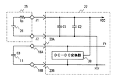
図6は、本発明の実施例2に係る電子スチルカメラに適用されるコンデンサを対応する回路ブロックと共に示す接続図である。この電子スチルカメラでは、実施例1について上述したと同様にして大容量のコンデンサ11が実装され、このコンデンサ11がこの図6に示す回路ブロックに適用される。なおこの実施例に係る電子スチルカメラは、この図6に係る構成が異なる点を除いて、実施例1の電子スチルカメラと同一に構成される。
FIG. 6 is a connection diagram showing capacitors applied to the electronic still camera according to the second embodiment of the present invention together with corresponding circuit blocks. In this electronic still camera, a large-
すなわちこの電子スチルカメラにおいては、配線基板22に実装されたDC−DC変換器38によりバッテリ25の電源を昇圧して所望の電圧による電源を生成するようになされ、コンデンサ11は、この電源の平滑用に適用される。
That is, in this electronic still camera, the DC-
この実施例のように平滑用に大容量のコンデンサを設ける場合であっても、実施例1と同一の効果を得ることができる。 Even when a large-capacitance capacitor is provided for smoothing as in this embodiment, the same effect as in the first embodiment can be obtained.
図7は、本発明の実施例3に係る電子スチルカメラに適用されるコンデンサを対応する回路ブロックと共に示す接続図である。この電子スチルカメラでは、実施例1について上述したと同様にして大容量のコンデンサ11が実装され、このコンデンサ11がこの図7に示す回路ブロックに適用される。なおこの実施例に係る電子スチルカメラは、この図7に係る構成が異なる点を除いて、実施例1の電子スチルカメラと同一に構成される。
FIG. 7 is a connection diagram showing capacitors applied to the electronic still camera according to the third embodiment of the present invention together with corresponding circuit blocks. In this electronic still camera, a large-
すなわちこの電子スチルカメラにおいては、配線基板22に入力されるバッテリ25による電源のデカップリング用にコンデンサ11が適用され、瞬時電流による電源電圧の降下を緩和する。
That is, in this electronic still camera, the
この実施例のようにデカップリング用のコンデンサを適用して、瞬時電流による電源電圧の降下を緩和する場合であっても、実施例1と同一の効果を得ることができる。 Even when a decoupling capacitor is applied as in this embodiment to reduce the power supply voltage drop due to the instantaneous current, the same effect as in the first embodiment can be obtained.
なお上述の実施例においては、断面Vの字形状による端子によりコンデンサを基板に接続する場合について述べたが、本発明はこれに限らず、端子の形状にあっては種々の形状を適用することができる。 In the above-described embodiment, the case where the capacitor is connected to the substrate by the terminal having the V-shaped cross section is described. However, the present invention is not limited to this, and various shapes can be applied to the terminal shape. It is Ru can.
また上述の実施例においては、それぞれ1つのコンデンサを外装内側面に配置する場合について述べたが、本発明はこれに限らず、複数のコンデンサを併設して、さらには重ね合わせて配置するようにしてもよい。またこの場合に、図6及び図7との対比により図8に示すように、2種類のコンデンサを一体化して複合型のコンデンサ41を形成し、このコンデンサ41を外装内側面に配置するようにしてもよい。
In the above-described embodiments, the case where one capacitor is arranged on the inner surface of the exterior has been described. However, the present invention is not limited to this, and a plurality of capacitors are also provided side by side. May be. Further, in this case, as shown in FIG. 8 in comparison with FIGS. 6 and 7, two types of capacitors are integrated to form a
また上述の実施例においては、酸化皮膜による誘電体膜を形成してなる陽極用電極、電解紙、陰極用電極による電解コンデンサに本発明を適用する場合について述べたが、本発明はこれに限らず、例えば電気二重層によるコンデンサ等、種々の電解コンデンサに広く適用することができる。 In the above-described embodiments, the case where the present invention is applied to an anode electrode formed by forming a dielectric film by an oxide film, electrolytic paper, and an electrolytic capacitor using a cathode electrode has been described. However, the present invention is not limited to this. For example, it can be widely applied to various electrolytic capacitors such as a capacitor using an electric double layer.
また上述の実施例においては、それぞれフラッシュの駆動用等にコンデンサを実装する場合について述べたが、本発明はこれに限らず、例えば、USB(Universal Serial Bus)により供給される電力を一次蓄積してハードディスクの起動に係る瞬時電流を補う場合等、要は大容量のコンデンサを実装する場合に広く適用することができる。 In the above-described embodiments, the case where a capacitor is mounted for driving a flash has been described. However, the present invention is not limited to this. For example, power supplied by a USB (Universal Serial Bus) is primarily accumulated. Thus, the present invention can be widely applied when a large-capacity capacitor is mounted, for example, when an instantaneous current related to the startup of a hard disk is compensated.
また上述の実施例においては、粘着剤による接着によりコンデンサを配置する場合について述べたが、本発明はこれに限らず、例えばエポキシ樹脂等の粘着剤による接着により配置する場合、ケースに設けた爪等によりケースに保持して配置する場合、さらにはケースとの一体成形によりケースに配置する場合等、種々の配置方法を広く適用することができる。 Further, in the above-described embodiments, the case where the capacitor is arranged by adhesion with an adhesive has been described. Various arrangement methods can be widely applied, for example, in a case where the arrangement is held in the case by means of, for example, or in the case where the arrangement is carried out by integral molding with the case.
また上述の実施例においては、本発明を電子スチルカメラに適用する場合について述べたが、本発明はこれに限らず、携帯電話、PDA、ビデオカメラ等、バッテリにより動作する携帯型の各種電子機器、さらには据え置き型の電子機器等に広く適用することができる。 In the above-described embodiments, the case where the present invention is applied to an electronic still camera has been described. However, the present invention is not limited to this, and various portable electronic devices that are operated by a battery, such as a mobile phone, a PDA, and a video camera. Further, it can be widely applied to stationary electronic devices.
本発明は、電子スチルカメラ、携帯電話、PDA等に適用することができる。 The present invention can be applied to an electronic still camera, a mobile phone, a PDA, and the like.
1……電子スチルカメラ、10A……正面ケース、10B……背面ケース、11、41……コンデンサ、16A……陽極用電極、16B……陰極用電極、18A、18B、23A、23B……端子、22……配線基板
DESCRIPTION OF SYMBOLS 1 ... Electronic still camera, 10A ... Front case, 10B ... Back case, 11, 41 ... Capacitor, 16A ... Electrode for anode, 16B ... Electrode for cathode, 18A, 18B, 23A, 23B ... Terminal , 22 …… Wiring board
Claims (6)
陽極用電極及び陰極用電極を交互に積層して平板形状に形成され、可撓性を有し、一方の面に前記陽極用電極及び陰極用電極に夫々接続された1対の端子が設けられ、他方の面が前記ケースの内面に接着されたコンデンサと、
前記ケース内に配置され、一方の面に電子部品が実装され、他方の面に弾性を有する1対の接触端子が設けられ、前記1対の接触端子で前記コンデンサの前記一方の面に設けた前記1対の端子を夫々押圧して前記電子部品による電子回路を前記コンデンサに接続する配線基板とを備える
電子機器。 Case and
An anode electrode and cathode electrode are laminated alternately formed in a flat plate shape, having flexibility, each connected pair of pin is provided on the anode electrode and cathode electrode on one surface A capacitor having the other surface bonded to the inner surface of the case;
An electronic component is mounted on one surface of the case, a pair of contact terminals having elasticity is provided on the other surface, and the pair of contact terminals are provided on the one surface of the capacitor. An electronic device comprising: a wiring board that presses the pair of terminals and connects an electronic circuit of the electronic component to the capacitor .
請求項1に記載の電子機器。 The electronic device according to claim 1, wherein the capacitor is a capacitor that reduces a drop in power supply voltage due to an instantaneous current of the electronic circuit.
請求項1に記載の電子機器。 The electronic device according to claim 1, wherein the capacitor is a capacitor for smoothing a power supply voltage of the electronic circuit.
請求項1に記載の電子機器。 The electronic device according to claim 1, wherein the capacitor is a capacitor that temporarily drives an electronic component constituting the electronic circuit by discharging charged power.
請求項4に記載の電子機器。 The electronic device according to claim 4, wherein the electronic component is a light emitting element.
一方の面に所望の電子部品が実装され、他方の面に弾性を有する1対の接触端子が設けられた配線基板をケース内に配置し、
前記弾性を有する1対の接触端子で前記コンデンサの前記一方の面に設けた前記1対の端子を夫々押圧して前記電子部品による電子回路を前記コンデンサに接続する
電子機器におけるコンデンサの実装方法。 The electrode for anode and the electrode for cathode are alternately laminated to form a flat plate shape, which is flexible and has a pair of terminals connected to the anode electrode and the cathode electrode on one surface. Bond the other side of the capacitor to the inner surface of the case,
A wiring board in which a desired electronic component is mounted on one surface and a pair of elastic contact terminals is provided on the other surface is disposed in the case.
A method of mounting a capacitor in an electronic device , wherein the pair of contact terminals having elasticity are pressed against the pair of terminals provided on the one surface of the capacitor to connect an electronic circuit of the electronic component to the capacitor.
Priority Applications (2)
| Application Number | Priority Date | Filing Date | Title |
|---|---|---|---|
| JP2003291947A JP4356393B2 (en) | 2003-08-12 | 2003-08-12 | Electronic device and method for mounting capacitor in electronic device |
| CNB2004100565643A CN100429729C (en) | 2003-08-12 | 2004-08-10 | Electronic device and capacitor, and method for mounting capacitor in said electronic device |
Applications Claiming Priority (1)
| Application Number | Priority Date | Filing Date | Title |
|---|---|---|---|
| JP2003291947A JP4356393B2 (en) | 2003-08-12 | 2003-08-12 | Electronic device and method for mounting capacitor in electronic device |
Publications (2)
| Publication Number | Publication Date |
|---|---|
| JP2005064212A JP2005064212A (en) | 2005-03-10 |
| JP4356393B2 true JP4356393B2 (en) | 2009-11-04 |
Family
ID=34369452
Family Applications (1)
| Application Number | Title | Priority Date | Filing Date |
|---|---|---|---|
| JP2003291947A Expired - Fee Related JP4356393B2 (en) | 2003-08-12 | 2003-08-12 | Electronic device and method for mounting capacitor in electronic device |
Country Status (2)
| Country | Link |
|---|---|
| JP (1) | JP4356393B2 (en) |
| CN (1) | CN100429729C (en) |
Family Cites Families (3)
| Publication number | Priority date | Publication date | Assignee | Title |
|---|---|---|---|---|
| US4356530A (en) * | 1979-12-15 | 1982-10-26 | Tdk Electronics Co., Ltd. | Ceramic capacitor |
| JPH0786081A (en) * | 1993-09-09 | 1995-03-31 | Mitsubishi Materials Corp | Manufacture of multilayered ceramic capacitor |
| JP2000243644A (en) * | 1999-02-19 | 2000-09-08 | Dainippon Printing Co Ltd | Manufacture of laminated capacitor |
-
2003
- 2003-08-12 JP JP2003291947A patent/JP4356393B2/en not_active Expired - Fee Related
-
2004
- 2004-08-10 CN CNB2004100565643A patent/CN100429729C/en not_active Expired - Fee Related
Also Published As
| Publication number | Publication date |
|---|---|
| CN100429729C (en) | 2008-10-29 |
| CN1582099A (en) | 2005-02-16 |
| JP2005064212A (en) | 2005-03-10 |
Similar Documents
| Publication | Publication Date | Title |
|---|---|---|
| US8415045B2 (en) | Electronic appliance secondary battery | |
| JP4006921B2 (en) | Thin battery | |
| KR102041590B1 (en) | Flexible electrode assembly, and rechargeable battery | |
| JP2013021347A (en) | Electrochemical device | |
| JP4864427B2 (en) | Manufacturing method of electric double layer capacitor | |
| US10910167B2 (en) | Electrochemical device and method for manufacturing same | |
| JP4356393B2 (en) | Electronic device and method for mounting capacitor in electronic device | |
| JP3579621B2 (en) | Battery pack | |
| US10879016B2 (en) | Electrochemical device and method for manufacturing same | |
| JP4019279B2 (en) | Battery, electronic device, and capacitor mounting method in electronic device | |
| CN113097568A (en) | Electrochemical device and electronic device using the same | |
| JP2001035465A (en) | Pack structure of flat battery | |
| JP4581340B2 (en) | Strobe device, driving method thereof, and electronic apparatus | |
| JP2005123127A (en) | Battery pack | |
| JP2001244156A (en) | Electrochemical capacitor | |
| JP2017084469A (en) | Battery pack and spacer for battery pack | |
| JP6155181B2 (en) | Flash light emitting device | |
| US6360060B1 (en) | Camera | |
| JP2010114365A (en) | Electric double layer capacitor and method of manufacturing the same | |
| JP2001223933A (en) | Electronic camera | |
| JP2003187755A (en) | Secondary battery manufacturing method and secondary battery | |
| JP6101373B2 (en) | Light emitting unit and flash light emitting device | |
| JP2001297951A (en) | Flat capacitor | |
| JP2002174846A (en) | Arrangement structure of main condenser for strobe device | |
| JP2008153516A (en) | Electric double layer capacitor |
Legal Events
| Date | Code | Title | Description |
|---|---|---|---|
| A621 | Written request for application examination |
Free format text: JAPANESE INTERMEDIATE CODE: A621 Effective date: 20050303 |
|
| A977 | Report on retrieval |
Free format text: JAPANESE INTERMEDIATE CODE: A971007 Effective date: 20080214 |
|
| A131 | Notification of reasons for refusal |
Free format text: JAPANESE INTERMEDIATE CODE: A131 Effective date: 20080227 |
|
| A521 | Request for written amendment filed |
Free format text: JAPANESE INTERMEDIATE CODE: A523 Effective date: 20080422 |
|
| A131 | Notification of reasons for refusal |
Free format text: JAPANESE INTERMEDIATE CODE: A131 Effective date: 20081030 |
|
| A521 | Request for written amendment filed |
Free format text: JAPANESE INTERMEDIATE CODE: A523 Effective date: 20081219 |
|
| RD03 | Notification of appointment of power of attorney |
Free format text: JAPANESE INTERMEDIATE CODE: A7423 Effective date: 20090331 |
|
| RD04 | Notification of resignation of power of attorney |
Free format text: JAPANESE INTERMEDIATE CODE: A7424 Effective date: 20090402 |
|
| TRDD | Decision of grant or rejection written | ||
| A01 | Written decision to grant a patent or to grant a registration (utility model) |
Free format text: JAPANESE INTERMEDIATE CODE: A01 Effective date: 20090714 |
|
| A01 | Written decision to grant a patent or to grant a registration (utility model) |
Free format text: JAPANESE INTERMEDIATE CODE: A01 |
|
| A61 | First payment of annual fees (during grant procedure) |
Free format text: JAPANESE INTERMEDIATE CODE: A61 Effective date: 20090727 |
|
| FPAY | Renewal fee payment (event date is renewal date of database) |
Free format text: PAYMENT UNTIL: 20120814 Year of fee payment: 3 |
|
| FPAY | Renewal fee payment (event date is renewal date of database) |
Free format text: PAYMENT UNTIL: 20120814 Year of fee payment: 3 |
|
| LAPS | Cancellation because of no payment of annual fees |