JP4342131B2 - Capacitance element manufacturing method and semiconductor device manufacturing method - Google Patents
Capacitance element manufacturing method and semiconductor device manufacturing method Download PDFInfo
- Publication number
- JP4342131B2 JP4342131B2 JP2001332706A JP2001332706A JP4342131B2 JP 4342131 B2 JP4342131 B2 JP 4342131B2 JP 2001332706 A JP2001332706 A JP 2001332706A JP 2001332706 A JP2001332706 A JP 2001332706A JP 4342131 B2 JP4342131 B2 JP 4342131B2
- Authority
- JP
- Japan
- Prior art keywords
- film
- heat treatment
- electrode
- capacitor
- upper electrode
- Prior art date
- Legal status (The legal status is an assumption and is not a legal conclusion. Google has not performed a legal analysis and makes no representation as to the accuracy of the status listed.)
- Expired - Lifetime
Links
Images


Classifications
-
- H—ELECTRICITY
- H10—SEMICONDUCTOR DEVICES; ELECTRIC SOLID-STATE DEVICES NOT OTHERWISE PROVIDED FOR
- H10D—INORGANIC ELECTRIC SEMICONDUCTOR DEVICES
- H10D84/00—Integrated devices formed in or on semiconductor substrates that comprise only semiconducting layers, e.g. on Si wafers or on GaAs-on-Si wafers
-
- H—ELECTRICITY
- H10—SEMICONDUCTOR DEVICES; ELECTRIC SOLID-STATE DEVICES NOT OTHERWISE PROVIDED FOR
- H10D—INORGANIC ELECTRIC SEMICONDUCTOR DEVICES
- H10D1/00—Resistors, capacitors or inductors
- H10D1/60—Capacitors
- H10D1/68—Capacitors having no potential barriers
- H10D1/692—Electrodes
-
- H—ELECTRICITY
- H10—SEMICONDUCTOR DEVICES; ELECTRIC SOLID-STATE DEVICES NOT OTHERWISE PROVIDED FOR
- H10B—ELECTRONIC MEMORY DEVICES
- H10B12/00—Dynamic random access memory [DRAM] devices
- H10B12/01—Manufacture or treatment
- H10B12/09—Manufacture or treatment with simultaneous manufacture of the peripheral circuit region and memory cells
-
- H—ELECTRICITY
- H10—SEMICONDUCTOR DEVICES; ELECTRIC SOLID-STATE DEVICES NOT OTHERWISE PROVIDED FOR
- H10B—ELECTRONIC MEMORY DEVICES
- H10B12/00—Dynamic random access memory [DRAM] devices
- H10B12/30—DRAM devices comprising one-transistor - one-capacitor [1T-1C] memory cells
- H10B12/31—DRAM devices comprising one-transistor - one-capacitor [1T-1C] memory cells having a storage electrode stacked over the transistor
- H10B12/315—DRAM devices comprising one-transistor - one-capacitor [1T-1C] memory cells having a storage electrode stacked over the transistor with the capacitor higher than a bit line
-
- H—ELECTRICITY
- H10—SEMICONDUCTOR DEVICES; ELECTRIC SOLID-STATE DEVICES NOT OTHERWISE PROVIDED FOR
- H10B—ELECTRONIC MEMORY DEVICES
- H10B12/00—Dynamic random access memory [DRAM] devices
- H10B12/30—DRAM devices comprising one-transistor - one-capacitor [1T-1C] memory cells
- H10B12/48—Data lines or contacts therefor
-
- H—ELECTRICITY
- H10—SEMICONDUCTOR DEVICES; ELECTRIC SOLID-STATE DEVICES NOT OTHERWISE PROVIDED FOR
- H10D—INORGANIC ELECTRIC SEMICONDUCTOR DEVICES
- H10D1/00—Resistors, capacitors or inductors
- H10D1/01—Manufacture or treatment
- H10D1/041—Manufacture or treatment of capacitors having no potential barriers
- H10D1/042—Manufacture or treatment of capacitors having no potential barriers using deposition processes to form electrode extensions
-
- H—ELECTRICITY
- H10—SEMICONDUCTOR DEVICES; ELECTRIC SOLID-STATE DEVICES NOT OTHERWISE PROVIDED FOR
- H10D—INORGANIC ELECTRIC SEMICONDUCTOR DEVICES
- H10D1/00—Resistors, capacitors or inductors
- H10D1/60—Capacitors
- H10D1/68—Capacitors having no potential barriers
- H10D1/692—Electrodes
- H10D1/711—Electrodes having non-planar surfaces, e.g. formed by texturisation
- H10D1/716—Electrodes having non-planar surfaces, e.g. formed by texturisation having vertical extensions
Landscapes
- Semiconductor Memories (AREA)
- Electrodes Of Semiconductors (AREA)
- Semiconductor Integrated Circuits (AREA)
Description
【0001】
【発明の属する技術分野】
本発明は、MIM(金属−絶縁膜−金属)構造を有する容量素子に係り、特に、熱処理による電極とキャパシタ誘電体膜との界面における膜剥がれやキャパシタ特性の劣化を防止しうる容量素子及びその製造方法並びにこのような容量素子を有する半導体装置の製造方法に関する。
【0002】
【従来の技術】
DRAMは、1トランジスタ、1キャパシタで構成しうる半導体記憶装置であり、従来より、高密度・高集積化された半導体記憶装置を製造するための構造や製造方法が種々検討されている。特に、キャパシタの占有面積はデバイスの集積化に多大な影響を与えるため、単位面積あたりの蓄積容量を如何にして増加するかが極めて重要である。このため、近年開発が行われているギガビット級の記憶容量を有するDRAMでは、キャパシタによる所有面積を狭めるべく、従来より広く用いられていたシリコン酸化膜やシリコン窒化膜よりも誘電率の大きな金属酸化物をキャパシタ誘電体膜として採用することが検討されている。このような酸化物誘電体膜としては、タンタル酸化膜、BSTO膜、STO膜、PZT膜などの酸化物誘電体膜が検討されている。
【0003】
キャパシタ誘電体膜としてこれら酸化物誘電体膜を用いる場合、通常、その成膜にはCVD法が用いられていた。これは、CVDにより形成した膜が高い誘電率を有すること、リーク電流が小さいこと及びステップカバレッジに優れた膜を形成できることによる。また、電極材料としては、ルテニウム(Ru)などの貴金属材料が用いられていた。これは、貴金属膜が酸化物誘電体膜との密着性に優れているとともに、仕事関数差が大きくリーク電流の小さいキャパシタを構成できるからである。
【0004】
【発明が解決しようとする課題】
しかしながら、本願発明者らが種々の検討を行ったところ、酸化物誘電体膜上に金属材料よりなる上部電極を形成した場合、その後に行う熱処理によって酸化物誘電体膜と上部電極との界面において膜剥がれが生じることが判明した。
【0005】
また、通常の半導体プロセスでは最上層のパッシベーション膜を形成した後にトランジスタの特性向上のためにフォーミングガス雰囲気中での熱処理を行うが、この熱処理によってキャパシタの電気特性が劣化することがあった。
【0006】
本発明の目的は、上部電極と酸化物誘電体膜との間における膜剥がれを防止するとともに、キャパシタ特性の劣化を抑制しうる半導体装置及びその製造方法を提供することにある。
【0007】
【課題を解決するための手段】
上記目的は、基板上に、金属よりなる下部電極を形成する工程と、前記下部電極上に、酸化物誘電体膜よりなるキャパシタ誘電体膜を形成する工程と、前記キャパシタ誘電体膜上に、金属膜をCVD法により堆積する工程と、前記金属膜の堆積後、水素を含む雰囲気中で熱処理を行う工程と、前記熱処理を行った後、前記金属膜をパターニングして前記金属膜よりなる上部電極を形成する工程とを有することを特徴とする容量素子の製造方法によって達成される。
【0010】
また、上記目的は、半導体基板上に、金属よりなる下部電極を形成する工程と、前記下部電極上に、酸化物誘電体膜よりなるキャパシタ誘電体膜を形成する工程と、前記キャパシタ誘電体膜上に、金属膜をCVD法により堆積する工程と、前記金属膜の堆積後、水素を含む雰囲気中で熱処理を行う工程と、前記熱処理を行った後、前記金属膜をパターニングして前記金属膜よりなる上部電極を形成する工程とを有することを特徴とする半導体装置の製造方法によっても達成される。
【0012】
【発明の実施の形態】
[本発明の原理]
上述の通り、酸化物誘電体膜上に金属材料よりなる上部電極を形成した場合、その後に行う熱処理によって酸化物誘電体膜と上部電極との界面において膜剥がれが生じることが判明した。
【0013】
膜剥がれが生じる原因は、キャパシタ誘電体膜と上部電極との間の密着性が低いことが原因していると考えられる。そこで、本願発明者らが密着性が劣化する原因について鋭意検討を行ったところ、上部電極を成膜する過程で膜中に取り込まれる炭素に起因するものと推測された。膜中に取り込まれる炭素は、上部電極を構成する有機金属原料に含まれるものであり、CVD法により上部電極を成膜する場合にあってはこれらを完全に除去することは困難である。
【0014】
そこで、本発明では、以下に示す2つの方法により、キャパシタ誘電体膜と上部電極との間の密着性を向上する。以下、キャパシタ誘電体膜をタンタル酸化膜により、上部電極をルテニウム膜により構成する場合を例にして、本発明を詳述する。
【0015】
第1の方法は、上部電極となるルテニウム膜の堆積後、このルテニウム膜のパターニング前に、フォーミングガス雰囲気中で熱処理を行う方法である。なお、ここで、フォーミングガスとは、水素ガスを含む窒素ガスやアルゴンガスにより構成される還元性のガスであって、水素10%も含むガスである。フォーミングガス雰囲気中で熱処理を行うことにより、ルテニウム膜中の炭素を効果的に除去することができる。これにより、ルテニウム膜とタンタル酸化膜との界面近傍における炭素濃度も大幅に低減され、ルテニウム膜とタンタル酸化膜との間の密着性を向上することができる。
【0016】
フォーミングガス雰囲気中での熱処理は、室温〜450℃程度の範囲で行うことが有効である。具体的な処理条件は、上部電極中に含まれる炭素濃度等に応じて適宜設定することが望ましい。
【0017】
図1は、フォーミングガス雰囲気中での熱処理前後におけるキャパシタ中の炭素及び酸素の分布を2次イオン質量分析法により測定した結果を示すグラフである。図示するように、フォーミングガス雰囲気中での熱処理を行うことにより、上部電極を構成するルテニウム膜中の炭素濃度を大幅に低減できることが判る。
【0018】
図2は上部電極の形成後に熱処理を行った試料を走査型電子顕微鏡により観察した結果を示す図である。図2(a)は上部電極の形成後に400℃1時間の窒素雰囲気中での熱処理(N2アニール)を行った場合、図2(b)は上部電極の形成後に400℃1時間のフォーミングガス雰囲気中での熱処理(FGA)と400℃1時間の窒素雰囲気中での熱処理(N2アニール)を行った場合である。
【0019】
図示するように、窒素雰囲気中での熱処理のみを行った試料では上部電極の表面に隆起した領域が観察されており、キャパシタ誘電体膜と上部電極との間で膜剥がれが生じていることが判る。一方、フォーミングガス雰囲気中の熱処理と窒素雰囲気中の熱処理とを行った試料では膜剥がれは観察されておらず、フォーミングガス雰囲気中で熱処理を行うことにより、その後に窒素雰囲気中で熱処理を行っても膜剥がれが生じないことが判った。
【0020】
表1は、熱処理条件と上部電極の膜剥がれとの関係をまとめたものである。
【0021】
【表1】
【0022】
一般に、フォーミングガス雰囲気中で行う熱処理はキャパシタの電気特性を劣化するものとして認識されている。しかしながら、本願発明者らが検討を行ったところ、ルテニウム膜の堆積後、パターニング前に行う熱処理では、むしろキャパシタの電気特性が向上することが初めて明らかとなった。
【0023】
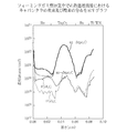
図3は、キャパシタのリーク電流を測定した結果を示すグラフである。図中、“As−Formed”はフォーミングガス雰囲気中で熱処理を行わない場合におけるキャパシタの電気特性を示しており、“FGA”はフォーミングガス雰囲気中で熱処理を行った場合におけるキャパシタの電気特性を示している。各条件に複数の線が含まれているのは、それぞれ29個のキャパシタの測定を行い、すべての特性を描いているためである。
【0024】
図示するように、フォーミングガス雰囲気中での熱処理を行っていない試料では、特性のばらつき及びリーク電流が大きい。しかしながら、フォーミングガス雰囲気中での熱処理を行うことにより、特性のばらつき及びリーク電流の双方を大幅に低減することができた。
【0025】
なお、フォーミングガス雰囲気中での熱処理は、上部電極を形成するためのパターニング前に行うことが重要である。上部電極を形成するためのパターニング後にフォーミングガス雰囲気中での熱処理を行ったのでは、キャパシタの電気特性の十分な向上は望めない。これに関しては明確なメカニズムは把握できていないが、フォーミングガス雰囲気中での熱処理の前にパターニングを行うと、ドライエッチングに用いられるF(フッ素)やCF4が試料表面に残存しており、この状態でフォーミングガス雰囲気中での熱処理を行うことにより雰囲気中にHFが生成され、タンタル酸化膜にダメージを与えているものと推測している。
【0026】
また、下部電極中の不純物濃度を軽減する観点から、下部電極の形成後、キャパシタ誘電体膜の形成前に、フォーミングガス雰囲気中で熱処理を行うようにしてもよい。
【0027】
第2の方法は、下部電極を構成するルテニウム膜の成膜条件と、上部電極を構成するルテニウム膜の成膜条件とを変える方法である。具体的には、下部電極の成膜は膜中に取り込まれる不純物(炭素や酸素)の濃度が低くなる条件で行い、上部電極の成膜は膜中の酸素濃度が高くなる条件で行う。
【0028】
図1から明らかなように、上部電極を形成した後に行うフォーミングガス雰囲気中での熱処理では、上部電極と比較して下部電極からの不純物の除去効果は小さい。したがって、下部電極の形成工程では、膜中に取り込まれる不純物の濃度が低くなる条件で行うことが望ましい。一方、上部電極中に高濃度に酸素が取り込まれると、酸化物であるキャパシタ誘電体膜との間の密着性が向上する。したがって、上部電極を形成する工程は、膜中の酸素濃度が高くなる条件でルテニウム膜を成膜することが望ましい。
【0029】
このように成膜条件を制御する1つの方法としては、ルテニウム膜の成膜温度を変化することが考えられる。ルテニウム原料としてRu(EtCp)2を用いる場合、例えば成膜温度を300℃とすると、膜中の酸素濃度は1×1021cm-3程度、炭素濃度は5×1020cm-3程度となり、例えば成膜温度を330℃とすると、膜中の酸素濃度は1×1020cm-3程度、炭素濃度は1×1020cm-3程度となる。したがって、上記の成膜条件を用いる場合、下部電極を330℃の成膜条件で形成し、上部電極を300℃の成膜条件を用いることにより、下部電極中の不純物濃度を低減しつつ、上部電極の密着性を向上することができる。
【0030】
或いは、上部電極を形成する際の酸素ガスに対するルテニウム原料の流量比を、下部電極を形成する際の酸素ガスに対するルテニウム原料の流量比よりも小さくすることによっても、上部電極中の酸素濃度を下部電極中の酸素濃度よりも高くすることができる。
【0031】
上部電極中に高濃度に酸素が含まれている場合、密着性向上に寄与するとともに、キャパシタの電気特性を向上するうえでも有効である。すなわち、上部電極中に含まれる酸素が後工程の熱処理によってキャパシタ誘電体膜中に拡散すると、タンタル酸化膜の組成を化学量論的組成に近づけるように作用する。これにより、良質のキャパシタ誘電体膜を形成することができる。
【0032】
なお、300℃の成膜条件を用いると、膜中に取り込まれる炭素濃度も増加する。この炭素を除去して更に密着性を向上する意味から、前述のフォーミングガス雰囲気中での熱処理を組み合わせることはより効果的である。
【0033】
また、本願発明者らがフォーミングガス雰囲気中での熱処理を行う時期に関して種々の検討を行ったところ、バックエンド工程中に行うフォーミングガス雰囲気中での熱処理がキャパシタの電気特性を向上するうえで有効であることがはじめて明らかとなった。具体的には、キャパシタ上を覆う層間絶縁膜、この層間絶縁膜を貫いて上部電極等に接続される電極プラグを形成した後にフォーミングガス雰囲気中での熱処理を行うことにより、キャパシタの電気特性を向上することができる。
【0034】
図4はキャパシタのリーク電流を測定した結果を示すグラフである。図中、“As−Formed”はキャパシタ及び電極プラグの形成直後、“FGA”はキャパシタ及び電極プラグの形成後にフォーミングガス雰囲気中での熱処理を行った場合、“FGA+N2”はキャパシタ及び電極プラグの形成後にフォーミングガス雰囲気中での熱処理と窒素雰囲気中での熱処理とを行った場合、“FGA+N2+FGA”はキャパシタ及び電極プラグの形成後にフォーミングガス雰囲気中での熱処理と窒素雰囲気中での熱処理とを行い、更にフォーミングガス雰囲気中での熱処理を行った場合の電気特性である。各条件に複数の線が含まれているのは、それぞれ3〜4個のキャパシタの測定を行い、すべての特性を描いているためである。
【0035】
図示するように、電極プラグを形成する一連のバックエンドプロセスを行うことにより、キャパシタの電気特性は劣化する。この劣化は、コンタクトホール形成過程におけるプラズマダメージなどによるものと考えられる。しかしながら、キャパシタのリーク電流は、フォーミングガス雰囲気中での熱処理を行うことにより大幅に低減する。特に、フォーミングガス雰囲気中での熱処理を行った後に窒素雰囲気中での熱処理を行う場合にあっては、リーク電流を更に低減することができる。
【0036】
バックエンドプロセスの最後にトランジスタの特性向上のために行われるフォーミングガス雰囲気中での熱処理を考慮して、キャパシタ及び電極プラグの形成後にフォーミングガス雰囲気中での熱処理と窒素雰囲気中での熱処理とを行い、更にフォーミングガス雰囲気中での熱処理を行った場合の電気特性は、フォーミングガス雰囲気中での熱処理と窒素雰囲気中での熱処理とを行った場合よりは劣化する。しかしながら、バックエンドプロセス中にフォーミングガスアニールを行わない場合(“As−formed”)よりも良好の電気特性を得られることが判った。
【0037】
[実施形態]
本発明の一実施形態による半導体装置及びその製造方法について図5乃至図18を用いて説明する。
【0038】
図5は本実施形態による半導体装置の構造を示す平面図、図6は本実施形態による半導体装置の構造を示す概略断面図、図7乃至図17は本実施形態による半導体装置の製造方法を示す工程断面図、図18は半導体装置の断面構造を走査型電子顕微鏡により観察した結果を示す図である。
【0039】
はじめに、本実施形態による半導体装置の構造を図5及び図6を用いて説明する。
【0040】
シリコン基板10上には、素子領域を画定する素子分離膜12が形成されている。素子領域上には、ゲート電極20とソース/ドレイン拡散層24、26とを有するメモリセルトランジスタが形成されている。ゲート電極20は、図5に示すように、ワード線を兼ねる導電膜としても機能する。メモリセルトランジスタが形成されたシリコン基板10上には、ソース/ドレイン拡散層24に接続されたプラグ36及びソース/ドレイン拡散層26に接続されたプラグ38とが埋め込まれた層間絶縁膜30が形成されている。
【0041】
層間絶縁膜30上には、層間絶縁膜40が形成されている。層間絶縁膜40上には、プラグ36を介してソース/ドレイン拡散層24に接続されたビット線48が形成されている。ビット線48は、図5に示すように、ワード線(ゲート電極20)と交わる方向に延在して複数形成されている。ビット線48が形成された層間絶縁膜40上には、層間絶縁膜58が形成されている。層間絶縁膜58には、プラグ38に接続されたプラグ62が埋め込まれている。
【0042】
層間絶縁膜58上には、エッチングストッパ膜64、層間絶縁膜66及びエッチングストッパ膜68が形成されている。エッチングストッパ膜68上には、エッチングストッパ膜68、層間絶縁膜66、エッチングストッパ膜64を貫きプラグ62に接続され、エッチングストッパ膜68上に突出して形成されたシリンダ状の蓄積電極76が形成されている。蓄積電極76上には、タンタル酸化膜(Ta2O5)よりなるキャパシタ誘電体膜78を介して、ルテニウム膜よりなるプレート電極88が形成されている。
【0043】
プレート電極88上には、TiN膜82、層間絶縁膜84,90が形成されている。層間絶縁膜90上には、プラグ96及びTiN膜82を介してプレート電極88に接続され、或いは、プラグ98を介してビット線48に接続された配線層100が形成されている。配線層100が形成された層間絶縁膜90上には、層間絶縁膜102が形成されている。
【0044】
こうして、1トランジスタ、1キャパシタよりなるメモリセルを有するDRAMが構成されている。
【0045】
ここで、本実施形態による半導体装置は、プレート電極88中の炭素濃度が、蓄積電極76中の炭素濃度よりも低くなっていることを1つの特徴とする。本発明による半導体装置においてプレート電極88中の炭素濃度が蓄積電極76中の炭素濃度よりも低いのは、前述のようにキャパシタ誘電体膜78とプレート電極88との間の密着性を高めるためである。電極中の炭素濃度をこのように制御することにより、後工程の熱処理による膜剥がれを防止することができる。
【0046】
なお、このような炭素濃度を有する電極構造は、プレート電極88となるルテニウム膜の堆積後、パターニング前に、フォーミングガス雰囲気中での熱処理を行うことにより形成することができる。
【0047】
次に、本実施形態による半導体装置の製造方法について図7乃至図17を用いて説明する。なお、図7及び図8は図5のA−A′線断面における工程断面図を表し、図9乃至図17は、図5のB−B′線断面における工程断面図を表している。
【0048】
まず、シリコン基板10の主表面上に、例えば、STI(Shallow Trench Isolation)法により、素子分離膜12を形成する(図7(a))。例えば、まず、シリコン基板10上に膜厚100nmのシリコン窒化膜(図示せず)を形成する。次いで、このシリコン窒化膜を、素子領域となる領域に残存するようにパターニングする。次いで、パターニングしたシリコン窒化膜をハードマスクとしてシリコン基板10をエッチングし、シリコン基板10に例えば深さ200nmの素子分離溝を形成する。次いで、例えばCVD法によりシリコン酸化膜を全面に堆積した後、シリコン窒化膜が露出するまでこのシリコン酸化膜をCMP(化学的機械的研磨:Chemical Mechanical Polishing)法により研磨し、素子分離溝内に選択的にシリコン酸化膜を残存させる。この後、シリコン窒化膜を除去し、シリコン基板10の素子分離溝に埋め込まれたシリコン酸化膜よりなる素子分離膜12を形成する。
【0049】
次いで、メモリセル領域のシリコン基板10中にPウェル(図示せず)を形成し、しきい値電圧制御のためのイオン注入を行う。
【0050】
次いで、素子分離膜12により画定された複数の素子領域上に、例えば熱酸化法により、例えば膜厚5nmのシリコン酸化膜よりなるゲート絶縁膜14を形成する。なお、ゲート絶縁膜14としては、シリコン窒化酸化膜などの他の絶縁膜を適用してもよい。
【0051】
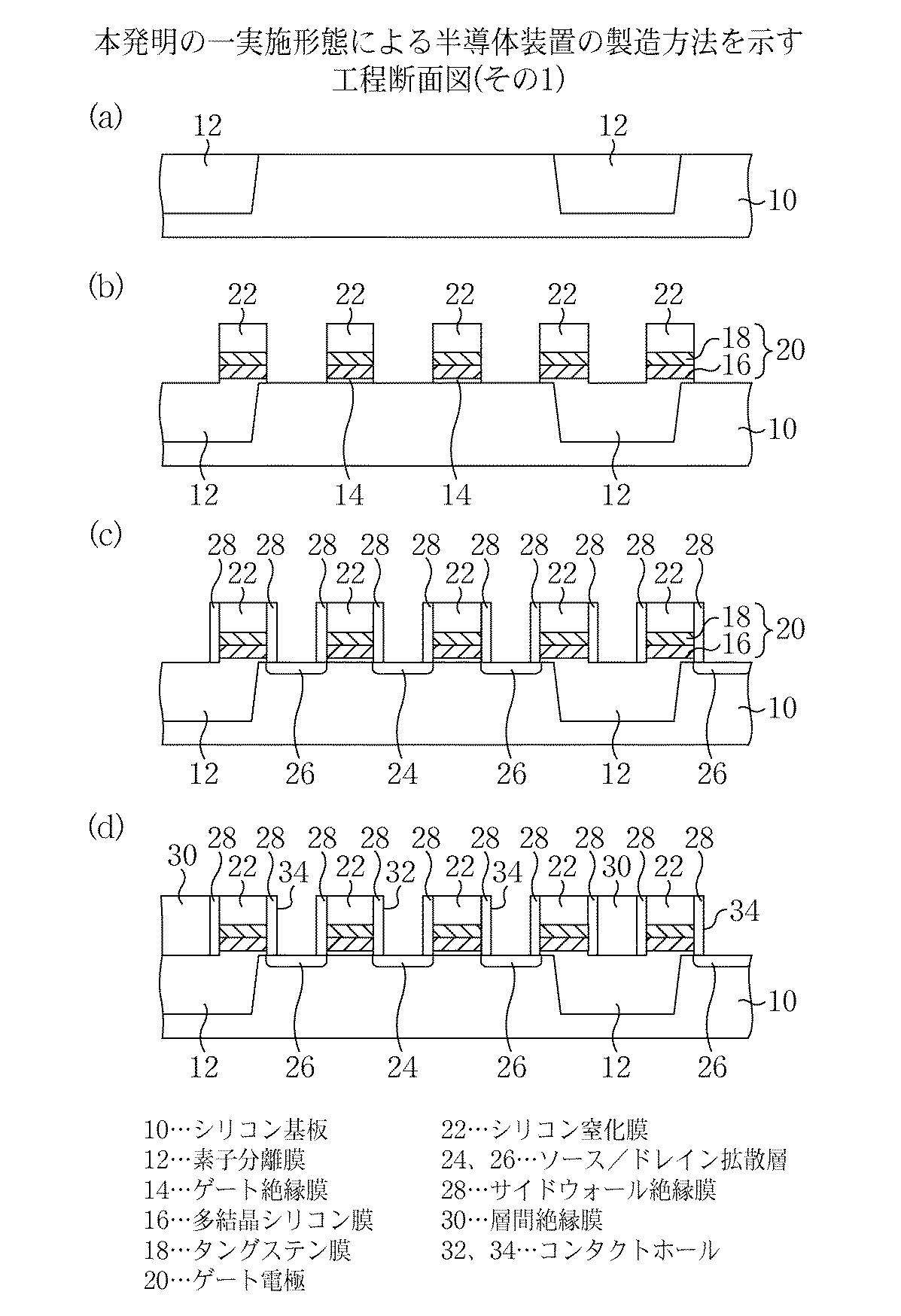
次いで、ゲート絶縁膜14上に、例えばポリシリコン膜16とタングステン膜18との積層膜よりなるポリメタル構造のゲート電極20を形成する(図7(b))。例えば、膜厚70nmのポリシリコン膜16と、膜厚5nmのタングステンナイトライド(WN)膜(図示せず)と、膜厚40nmのタングステン膜18と、膜厚200nmのシリコン窒化膜22とを順次堆積した後、リソグラフィー技術及びエッチング技術によりこれら膜を同一の形状にパターニングし、上面がシリコン窒化膜22で覆われ、タングステンナイトライド膜を介してポリシリコン膜16及びタングステン膜18が積層されてなるポリメタル構造のゲート電極20を形成する。なお、ゲート電極20は、ポリメタル構造に限られるものではなく、ポリゲート構造、ポリサイド構造、或いは、金属ゲート等を適用してもよい。
【0052】
次いで、ゲート電極20をマスクとしてイオン注入を行い、ゲート電極20の両側のシリコン基板10中にソース/ドレイン拡散層24、26を形成する。
【0053】
こうして、シリコン基板10上に、ゲート電極20、ソース/ドレイン拡散層24、26を有するメモリセルトランジスタを形成する。
【0054】
次いで、全面に、例えばCVD法により、例えば膜厚35nmのシリコン窒化膜を堆積した後にエッチバックし、ゲート電極20及びシリコン窒化膜22の側壁にシリコン窒化膜よりなるサイドウォール絶縁膜28を形成する(図7(c)、図9(a))。
【0055】
次いで、全面に、例えばCVD法により例えばBPSG膜を堆積した後、リフロー法及びCMP法等により、シリコン窒化膜18が露出するまでその表面を研磨し、表面が平坦化されたBPSG膜よりなる層間絶縁膜30を形成する。
【0056】
次いで、リソグラフィー技術及びエッチング技術により、層間絶縁膜30に、ソース/ドレイン拡散層24に達するスルーホール32と、ソース/ドレイン拡散層26に達するコンタクトホール34とを、ゲート電極20及びサイドウォール絶縁膜28に対して自己整合的に形成する(図7(d)、図9(b))。
【0057】
次いで、層間絶縁膜30に開口されたコンタクトホール32、34内に、プラグ36、38をそれぞれ埋め込む(図8(a)、図9(c))。例えば、CVD法により、砒素ドープした多結晶シリコン膜を堆積した後、CMP法によりシリコン窒化膜22が露出するまで研磨し、コンタクトホール32、34内のみに多結晶シリコン膜よりなるプラグ36、38を選択的に残存させる。
【0058】
次いで、全面に、例えばCVD法により、例えば膜厚200nmのシリコン酸化膜を堆積し、シリコン酸化膜よりなる層間絶縁膜40を形成する。
【0059】
次いで、リソグラフィー技術及びエッチング技術により、プラグ36に達するコンタクトホール42を層間絶縁膜40に形成する(図8(b)、図9(d))。
【0060】
次いで、層間絶縁膜40上に、コンタクトホール42を介してプラグ36に接続されたビット線48を形成する(図8(c)、図10(a))。例えば、まず、スパッタ法により、膜厚45nmの窒化チタン(TiN)/チタン(Ti)の積層構造よりなる密着層50と、膜厚250nmのタングステン(W)膜51とを順次堆積する。次いで、CMP法によりタングステン膜51を研磨し、コンタクトホール42内にタングステン膜51よりなるプラグを埋め込む。次いで、スパッタ法により、膜厚30nmのタングステン膜52を堆積する。次いで、CVD法により、タングステン膜52上に、膜厚200nmのシリコン窒化膜54を堆積する。次いで、リソグラフィー技術及びエッチング技術により、シリコン窒化膜54、タングステン膜52及び密着層50をパターニングし、上面がシリコン窒化膜54に覆われ、密着層50及びタングステン膜52よりなり、プラグ36を介してソース/ドレイン拡散層24に接続されたビット線48を形成する。
【0061】
次いで、全面に、例えばCVD法により、例えば膜厚20nmのシリコン窒化膜を堆積した後にエッチバックし、ビット線48及びシリコン窒化膜54の側壁に、シリコン窒化膜よりなるサイドウォール絶縁膜56を形成する(図10(b))。
【0062】
次いで、全面に、例えばCVD法により、例えば膜厚400nmのシリコン酸化膜を堆積し、CMP法によりその表面を研磨し、表面が平坦化されたシリコン酸化膜よりなる層間絶縁膜58を形成する。
【0063】
次いで、リソグラフィー技術及びエッチング技術により、層間絶縁膜58、40に、プラグ38に達するコンタクトホール60を形成する(図10(c))。このとき、シリコン窒化膜に対して高い選択比をもつエッチング条件でシリコン酸化膜をエッチングすることにより、ビット線48上を覆うシリコン窒化膜54及びビット線48の側壁に形成されたサイドウォール絶縁膜56に自己整合でコンタクトホール60を開口することができる。
【0064】
次いで、全面に、例えばスパッタ法により、膜厚25nmの窒化チタン/チタンの積層構造よりなる密着層と、膜厚250nmのタングステン膜とを堆積した後、層間絶縁膜58の表面が露出するまでCMP法により研磨し、コンタクトホール60内に埋め込まれたプラグ62を形成する(図11(a))。
【0065】
次いで、全面に、例えばCVD法により、例えば膜厚40nm程度のシリコン窒化膜を堆積し、シリコン窒化膜よりなるエッチングストッパ膜64を形成する。
【0066】
次いで、エッチングストッパ膜64上に、例えばCVD法により、例えば膜厚100nmのシリコン酸化膜を堆積し、シリコン酸化膜よりなる層間絶縁膜66を形成する。
【0067】
次いで、層間絶縁膜66上に、例えばCVD法により、例えば膜厚40nm程度のシリコン窒化膜を堆積し、シリコン窒化膜よりなるエッチングストッパ膜68を形成する。
【0068】
次いで、エッチングストッパ膜68上に、例えばCVD法により、例えば膜厚600nmのシリコン酸化膜を堆積し、シリコン酸化膜よりなる層間絶縁膜70を形成する(図11(b))。
【0069】
次いで、リソグラフィー技術及びエッチング技術により、層間絶縁膜70、エッチングストッパ膜68、層間絶縁膜66、エッチングストッパ膜64をパターニングし、蓄積電極の形成予定領域に、これら膜を貫いてプラグ62に達する開口部72を形成する(図12(a))。
【0070】
次いで、全面に、例えばCVD法により、膜厚10nmの窒化チタン膜と、膜厚40nmのルテニウム(Ru)膜とを堆積する。ルテニウム膜の成膜には、ルテニウム原料として例えばRu(EtCp)2を用い、330℃の温度で成膜を行う。この条件を用いることにより、ルテニウム膜中の酸素濃度は例えば1×1020cm-3程度、炭素濃度は例えば1×1020cm-3程度となる。
【0071】
次いで、フォトレジスト膜(図示せず)を塗布し、窒化チタン膜及びルテニウム膜が形成された開口部72内を埋め込む。
【0072】
次いで、例えばCMP法及び反応性イオンエッチング法により、層間絶縁膜70の表面が露出するまでフォトレジスト膜、ルテニウム膜及び窒化チタン膜を研磨するとともに、開口部72内のフォトレジスト膜を除去し、開口部72の内壁に沿って形成され、窒化チタン膜よりなる密着層74と、ルテニウム膜よりなる蓄積電極76とを形成する(図12(b))。
【0073】
次いで、例えば弗酸水溶液を用いたウェットエッチングなどの等方性エッチングにより、エッチングストッパ膜68をストッパとして、層間絶縁膜70を選択的にエッチングする。
【0074】
次いで、密着層74を、例えば硫酸と過酸化水素とを含む水溶液により、蓄積電極76、エッチングストッパ膜68、層間絶縁膜66に対して選択的にエッチングする(図13(a))。このエッチングは、密着層74と後に形成するキャパシタ誘電体膜78との相性が悪い場合を考慮したものであり、密着層74と蓄積電極76との相性がよい場合には、必ずしも密着層74を除去する必要はない。密着層74のエッチングは、少なくともエッチングストッパ膜68と蓄積電極76との間に間隙が形成されるまで行うことが望ましい。なお、キャパシタ誘電体膜との相性に基づいて密着層を除去する技術については、例えば、同一出願人による特開2000−124423号公報に詳述されている。
【0075】
次いで、全面に、例えばCVD法により、例えば膜厚10〜30nmのタンタル酸化膜を堆積し、このタンタル酸化膜よりなるキャパシタ誘電体膜78を形成する(図13(b))。例えば、酸素とペントエトキシタンタル(Ta(OC2H5)5)との混合ガスを用い、基板温度を480℃、圧力を1.3Torrとして成膜を行い、タンタル酸化膜よりなるキャパシタ誘電体膜78を形成する。
【0076】
次いで、UV−O3、O3或いはH2O雰囲気などにおける熱処理を行い、タンタル酸化膜中の酸素空孔を充填するとともに、PETの加水分解反応を促進する。例えば、UV−O3中で、温度を480℃として2時間の熱処理を行う。
【0077】
次いで、全面に、例えばCVD法により、例えば膜厚30〜50nmのルテニウム膜80を堆積する。例えば、スパッタ法により膜厚約10nmのシード層を形成した後、CVD法によりルテニウム膜を堆積することにより、所定膜厚のルテニウム膜を形成する。CVDによるルテニウム膜成の成膜には、ルテニウム原料として例えばRu(EtCp)2を用い、300℃の温度で成膜を行う。この条件を用いることにより、ルテニウム膜中の酸素濃度は例えば1×1021cm-3程度、炭素濃度は例えば5×1020cm-3程度となる。このような条件を用いた成膜では、膜中に多量の酸素が含まれており、キャパシタ誘電体膜78とルテニウム膜80との間の密着性は向上される。
【0078】
次いで、フォーミングガス(3%H2+97%N2)雰囲気中で例えば400℃、1時間の熱処理を行い、ルテニウム膜80中の不純物を低減する。熱処理後のルテニウム膜中の不純物分布は、例えば図1に示すようになる。これにより、キャパシタ誘電体膜78とルテニウム膜80(プレート電極88)との間の密着性が更に向上される。
【0079】
次いで、全面に、例えばスパッタ法により、例えば膜厚50nmのTiN膜82を堆積する。なお、TiN膜82は、プレート電極88とプラグ96との間の密着性を向上するための膜である。
【0080】
次いで、全面に、例えばCVD法により、例えば膜厚300nmのシリコン酸化膜を堆積し、シリコン酸化膜よりなる層間絶縁膜84を形成する(図14)。
【0081】
次いで、リソグラフィー技術及びエッチング技術により、層間絶縁膜84、TiN膜82、ルテニウム膜80をパターニングし、上面がTiN膜82及び層間絶縁膜84により覆われ、ルテニウム膜80よりなるプレート電極88を形成する。
【0082】
次いで、全面に、例えばCVD法により、例えば膜厚1000nmのシリコン酸化膜を堆積し、CMP法によりその表面を研磨し、表面が平坦化されたシリコン酸化膜よりなる層間絶縁膜90を形成する。
【0083】
次いで、リソグラフィー技術及びエッチング技術により、層間絶縁膜90を貫きプレート電極88に達するコンタクトホール92と、層間絶縁膜90、エッチングストッパ膜68、層間絶縁膜66、エッチングストッパ膜64及びシリコン窒化膜54を貫きビット線48に達するコンタクトホール94とを形成する(図15)。例えば、層間絶縁膜90,84,66は、圧力を0.05Torr、パワーを1500W、ガス流量をC4F8/CO/Ar/O2=15/300/350/5sccmとして、シリコン窒化膜に対してエッチング選択性を確保しうる条件でエッチングし、エッチングストッパ膜68、64及びシリコン窒化膜54は、圧力を0.05Torr、パワーを1500W、ガス流量をCHF3/CO/O2=50/150/5sccmとして、シリコン酸化膜に対してエッチング選択性を確保しうる条件でエッチングする。
【0084】
次いで、全面に、例えばスパッタ法により、膜厚25nmの窒化チタン/チタンの積層構造よりなる密着層と、膜厚250nmのタングステン膜とを堆積した後、層間絶縁膜90の表面が露出するまでCMP法により研磨し、コンタクトホール92内に埋め込まれたプラグ96と、コンタクトホール94内に埋め込まれたプラグ98とを形成する(図16)。
【0085】
次いで、フォーミングガス(3%H2+97%N2)雰囲気中で、例えば400℃、1時間の熱処理を行う。続けて、窒素雰囲気中で、例えば500℃、1時間の熱処理を行う。これら熱処理により、プラグ96,98を形成するまでのバックエンドプロセスにおいてキャパシタが被るダメージを低減し、キャパシタの特性を向上することができる。
【0086】
次いで、全面に、例えばスパッタ法により、膜厚10nmのバリアメタルとなる窒化チタン膜と、膜厚300nmのアルミ膜或いは銅膜とを堆積してパターニングし、プラグ96、98を介して下層配線に接続された配線層100を形成する。
【0087】
次いで、全面に、例えばCVD法により、例えば膜厚1000nmのシリコン酸化膜を堆積し、CMP法によりその表面を研磨し、表面が平坦化されたシリコン酸化膜よりなる層間絶縁膜102を形成する(図16)。
【0088】
次いで、リソグラフィー技術及びエッチング技術により、層間絶縁膜102を貫き配線層100に達するコンタクトホール104を形成する。
【0089】
次いで、全面に、例えばスパッタ法により、膜厚25nmの窒化チタン/チタンの積層構造よりなる密着層と、膜厚250nmのタングステン膜とを堆積した後、層間絶縁膜102の表面が露出するまでCMP法により研磨し、コンタクトホール104内に埋め込まれたプラグ106を形成する。
【0090】
次いで、全面に、例えばスパッタ法により、膜厚10nmのバリアメタルとなる窒化チタン膜と、膜厚300nmのアルミ膜或いは銅膜とを堆積してパターニングし、プラグ106を介して配線層100に接続された配線層108を形成する。
【0091】
次いで、全面に、例えばCVD法により、例えば膜厚300nmシリコン酸化膜110と、例えば膜厚600nmのシリコン窒化膜112とを堆積し、最上層のパッシベーション膜を形成する(図17)。
【0092】
次いで、フォーミングガス(3%H2+97%N2)雰囲気中で、例えば400℃、1時間の熱処理を行い、トランジスタ特性の回復を行う。
【0093】
こうして、1トランジスタ、1キャパシタよりなるメモリセルを有するDRAMを製造することができる。
【0094】
図18は、半導体装置の断面構造を走査型電子顕微鏡により観察した結果を示す図である。図18(a)はキャパシタの形成後に窒素雰囲気中で400℃、1時間の熱処理を行った試料、図18(b)はキャパシタの形成後にフォーミングガス雰囲気中で400℃、1時間の熱処理を行い、更に窒素雰囲気中で400℃、1時間の熱処理を行った試料である。
【0095】
図示するように、窒素雰囲気中での熱処理のみを行った試料ではキャパシタ誘電体膜78とプレート電極88との界面で膜剥がれが生じているが、フォーミングガス雰囲気中での熱処理及び窒素雰囲気中での熱処理を行った試料では膜剥がれは生じなかった。
【0096】
このように、本実施形態によれば、キャパシタ誘電体膜とプレート電極との界面における膜剥がれを防止できるとともに、フォーミングガス雰囲気中での熱処理によるキャパシタの電気特性の劣化を低減することができる。
【0097】
なお、上記実施形態では、蓄積電極及びプレート電極の形成条件の最適化、プレート電極となるルテニウム膜の成膜後、パターニングの前に行うフォーミングガス雰囲気中での熱処理及びバックエンドプロセス中に行うフォーミングガス雰囲気中での熱処理を行うことにより、キャパシタ誘電体膜とプレート電極との界面における密着性及びキャパシタの電気特性を向上したが、いずれか1つの手段のみを行うようにしてもよいし、任意の2つの手段を組み合わせて行うようにしてもよい。
【0098】
また、蓄積電極の形成後、キャパシタ誘電体膜の形成前に、フォーミングガス雰囲気中での熱処理を更に追加してもよい。この熱処理を行うことにより、蓄積電極中の不純物濃度を低減することができ、キャパシタ特性を向上することが可能である。
【0099】
[変形実施形態]
本発明は、上記実施形態に限らず種々の変形が可能である。
【0100】
例えば、上記実施形態では、キャパシタ誘電体膜としてタンタル酸化膜を用い、電極材料としてルテニウム膜を用いた場合を代表的な例として示しているが、本発明はタンタル酸化膜とルテニウム膜との組み合わせに限定されるものではない。
【0101】
電極材料としては、上記ルテニウムと共通の性質を有する白金族元素である、イリジウム(Ir)、ロジウム(Rh)、プラチナ(Pt)、パラジウム(Pd)、オスミウム(Os)を用いた場合に効果が期待できる。また、これら金属の酸化物である酸化ルテニウム(RuOx)や酸化イリジウム(IrOx)、SROを電極材料として用いてもよい。
【0102】
また、タンタル酸化膜を形成する場合のほか、上記導電性材料を電極材として用いる酸化物誘電体材料、例えば酸化ジルコニウム(ZrOx)膜、酸化ハフニウム(HfOx)膜、BST膜、STO膜、PZT膜を形成する場合においても、本発明を適用することができる。
【0103】
また、上記実施形態では、本発明をDRAMに適用した場合について説明したが、DRAMのみならず、MIM構造のキャパシタを有する半導体装置に広く適用することができる。例えば、キャパシタ誘電体膜として強誘電体膜を用いた強誘電体メモリにおいても本発明を適用することができる。
【0104】
【発明の効果】
以上の通り、本発明によれば、上部電極となる金属膜の堆積後、パターニングの前に、水素を含む雰囲気中での熱処理を行うので、上部電極中の炭素濃度が低減され、キャパシタ誘電体膜と上部電極との間の密着性を高めることができる。これにより、上部電極の膜剥がれを防止することができる。
【0105】
また、上部電極中に酸素が高濃度に含まれる条件で上部電極となる金属膜の成膜を行うので、キャパシタ誘電体膜と上部電極との間の密着性を高めることができる。これにより、上部電極の膜剥がれを防止することができる。
【0106】
また、上部電極の形成後、最上層のパッシベーション膜の形成前に、水素を含む雰囲気中で熱処理を行うので、バックエンドプロセスにおけるダメージを低減することができ、キャパシタ特性を向上することができる。
【図面の簡単な説明】
【図1】フォーミングガス雰囲気中での熱処理前後におけるキャパシタ中の炭素及び酸素の分布を2次イオン質量分析法により測定した結果を示すグラフである。
【図2】上部電極の形成後に熱処理を行った試料を走査型電子顕微鏡により観察した結果を示す図である。
【図3】キャパシタのリーク電流を測定した結果を示すグラフである。
【図4】キャパシタのリーク電流を測定した結果を示すグラフである。
【図5】本発明の一実施形態による半導体装置の構造を示す平面図である。
【図6】本発明の一実施形態による半導体装置の構造を示す概略断面図である。
【図7】本発明の一実施形態による半導体装置の製造方法を示す工程断面図(その1)である。
【図8】本発明の一実施形態による半導体装置の製造方法を示す工程断面図(その2)である。
【図9】本発明の一実施形態による半導体装置の製造方法を示す工程断面図(その3)である。
【図10】本発明の一実施形態による半導体装置の製造方法を示す工程断面図(その4)である。
【図11】本発明の一実施形態による半導体装置の製造方法を示す工程断面図(その5)である。
【図12】本発明の一実施形態による半導体装置の製造方法を示す工程断面図(その6)である。
【図13】本発明の一実施形態による半導体装置の製造方法を示す工程断面図(その7)である。
【図14】本発明の一実施形態による半導体装置の製造方法を示す工程断面図(その8)である。
【図15】本発明の一実施形態による半導体装置の製造方法を示す工程断面図(その9)である。
【図16】本発明の一実施形態による半導体装置の製造方法を示す工程断面図(その10)である。
【図17】本発明の一実施形態による半導体装置の製造方法を示す工程断面図(その11)である。
【図18】半導体装置の断面構造を走査型電子顕微鏡により観察した結果を示す図である。
【符号の説明】
10…シリコン基板
12…素子分離膜
14…ゲート絶縁膜
16…多結晶シリコン膜
18,52…タングステン膜
20…ゲート電極
22、54…シリコン窒化膜
24、26…ソース/ドレイン拡散層
28、56…サイドウォール絶縁膜
30、40、58、66、70、84、90、102…層間絶縁膜
32、34、60、92、94、104…コンタクトホール
36、38、62、96、98、106…プラグ
48…ビット線
50、74…密着層
64、68…エッチングストッパ膜
72…開口部
76…蓄積電極
78…キャパシタ誘電体膜
80…ルテニウム膜
82…TiN膜
88…プレート電極
100、108…配線層
112…シリコン酸化膜
114…シリコン窒化膜[0001]
BACKGROUND OF THE INVENTION
The present invention relates to a capacitive element having an MIM (metal-insulating film-metal) structure, and in particular, a capacitive element capable of preventing film peeling and deterioration of capacitor characteristics at the interface between an electrode and a capacitor dielectric film due to heat treatment, and a capacitor element thereof The present invention relates to a manufacturing method and a manufacturing method of a semiconductor device having such a capacitor element.
[0002]
[Prior art]
A DRAM is a semiconductor memory device that can be composed of one transistor and one capacitor. Conventionally, various structures and manufacturing methods for manufacturing a semiconductor memory device with high density and high integration have been studied. In particular, since the area occupied by the capacitor has a great influence on the integration of the device, how to increase the storage capacity per unit area is extremely important. For this reason, in a DRAM having a storage capacity of gigabit class that has been developed in recent years, a metal oxide having a dielectric constant larger than that of a silicon oxide film or a silicon nitride film that has been widely used so far in order to reduce the area owned by the capacitor. It has been studied to employ a material as a capacitor dielectric film. As such oxide dielectric films, oxide dielectric films such as tantalum oxide films, BSTO films, STO films, and PZT films have been studied.
[0003]
When these oxide dielectric films are used as the capacitor dielectric film, the CVD method is usually used for the film formation. This is because a film formed by CVD has a high dielectric constant, a leakage current is small, and a film excellent in step coverage can be formed. In addition, a noble metal material such as ruthenium (Ru) has been used as the electrode material. This is because the noble metal film is excellent in adhesion with the oxide dielectric film, and a capacitor having a large work function difference and a small leakage current can be formed.
[0004]
[Problems to be solved by the invention]
However, when the inventors of the present application have made various studies, when the upper electrode made of a metal material is formed on the oxide dielectric film, the heat treatment performed thereafter is performed at the interface between the oxide dielectric film and the upper electrode. It was found that film peeling occurred.
[0005]
In a normal semiconductor process, a heat treatment is performed in a forming gas atmosphere to improve the transistor characteristics after the uppermost passivation film is formed. This heat treatment sometimes deteriorates the electrical characteristics of the capacitor.
[0006]
An object of the present invention is to provide a semiconductor device capable of preventing film peeling between an upper electrode and an oxide dielectric film and suppressing deterioration of capacitor characteristics, and a method for manufacturing the same.
[0007]
[Means for Solving the Problems]
The above objects include a step of forming a lower electrode made of metal on a substrate, a step of forming a capacitor dielectric film made of an oxide dielectric film on the lower electrode, and on the capacitor dielectric film, A step of depositing a metal film by a CVD method, a step of performing a heat treatment in an atmosphere containing hydrogen after the deposition of the metal film, After performing the heat treatment, And a step of patterning the metal film to form an upper electrode made of the metal film.
[0010]
Also, the object is to form a lower electrode made of metal on a semiconductor substrate, to form a capacitor dielectric film made of an oxide dielectric film on the lower electrode, and to form the capacitor dielectric film A step of depositing a metal film by a CVD method, and a step of performing a heat treatment in an atmosphere containing hydrogen after the metal film is deposited; After performing the heat treatment, This method is also achieved by a method of manufacturing a semiconductor device, comprising patterning the metal film to form an upper electrode made of the metal film.
[0012]
DETAILED DESCRIPTION OF THE INVENTION
[Principle of the present invention]
As described above, when an upper electrode made of a metal material is formed on an oxide dielectric film, it has been found that film peeling occurs at the interface between the oxide dielectric film and the upper electrode by a subsequent heat treatment.
[0013]
The cause of film peeling is considered to be due to low adhesion between the capacitor dielectric film and the upper electrode. Therefore, the inventors of the present application conducted extensive studies on the cause of the deterioration of the adhesion, and it was assumed that it was caused by carbon incorporated into the film during the process of forming the upper electrode. Carbon incorporated into the film is contained in the organic metal raw material constituting the upper electrode, and it is difficult to completely remove the upper electrode when the upper electrode is formed by the CVD method.
[0014]
Therefore, in the present invention, the adhesion between the capacitor dielectric film and the upper electrode is improved by the following two methods. Hereinafter, the present invention will be described in detail by taking as an example the case where the capacitor dielectric film is made of a tantalum oxide film and the upper electrode is made of a ruthenium film.
[0015]
The first method is a method in which a heat treatment is performed in a forming gas atmosphere after the ruthenium film serving as the upper electrode is deposited and before the ruthenium film is patterned. Here, the forming gas is a reducing gas composed of nitrogen gas or argon gas containing hydrogen gas, and is a gas containing 10% hydrogen. By performing heat treatment in the forming gas atmosphere, carbon in the ruthenium film can be effectively removed. Thereby, the carbon concentration in the vicinity of the interface between the ruthenium film and the tantalum oxide film is also greatly reduced, and the adhesion between the ruthenium film and the tantalum oxide film can be improved.
[0016]
It is effective to perform the heat treatment in the forming gas atmosphere in the range of room temperature to about 450 ° C. It is desirable to set the specific processing conditions as appropriate in accordance with the carbon concentration contained in the upper electrode.
[0017]
FIG. 1 is a graph showing the results of measuring the distribution of carbon and oxygen in a capacitor before and after heat treatment in a forming gas atmosphere by secondary ion mass spectrometry. As shown in the figure, it is understood that the carbon concentration in the ruthenium film constituting the upper electrode can be significantly reduced by performing the heat treatment in the forming gas atmosphere.
[0018]
FIG. 2 is a diagram showing the results of observation of a sample subjected to heat treatment after formation of the upper electrode with a scanning electron microscope. FIG. 2A shows a heat treatment in a nitrogen atmosphere at 400 ° C. for 1 hour (N 2 2 (b) shows a heat treatment (FGA) in a forming gas atmosphere at 400 ° C. for 1 hour and a heat treatment (N in a nitrogen atmosphere at 400 ° C. for 1 hour) after the formation of the upper electrode. 2 This is a case where annealing is performed.
[0019]
As shown in the figure, in the sample subjected only to the heat treatment in the nitrogen atmosphere, a raised region is observed on the surface of the upper electrode, and there is a film peeling between the capacitor dielectric film and the upper electrode. I understand. On the other hand, film peeling was not observed in the samples subjected to the heat treatment in the forming gas atmosphere and the heat treatment in the nitrogen atmosphere, and by performing the heat treatment in the forming gas atmosphere, the heat treatment was performed in the nitrogen atmosphere thereafter. It was also found that no film peeling occurred.
[0020]
Table 1 summarizes the relationship between the heat treatment conditions and the film peeling of the upper electrode.
[0021]
[Table 1]
[0022]
In general, heat treatment performed in a forming gas atmosphere is recognized as degrading the electrical characteristics of the capacitor. However, as a result of investigations by the inventors of the present application, it has been clarified for the first time that the electrical characteristics of the capacitor are rather improved by the heat treatment performed after the deposition of the ruthenium film and before the patterning.
[0023]
FIG. 3 is a graph showing the result of measuring the leakage current of the capacitor. In the figure, “As-Formed” indicates the electrical characteristics of the capacitor when heat treatment is not performed in the forming gas atmosphere, and “FGA” indicates the electrical characteristics of the capacitor when heat treatment is performed in the forming gas atmosphere. ing. A plurality of lines are included in each condition because 29 capacitors are measured and all characteristics are drawn.
[0024]
As shown in the figure, in the sample not subjected to the heat treatment in the forming gas atmosphere, the characteristic variation and the leakage current are large. However, by performing the heat treatment in the forming gas atmosphere, both the characteristic variation and the leakage current can be greatly reduced.
[0025]
It is important to perform the heat treatment in the forming gas atmosphere before patterning for forming the upper electrode. If the heat treatment in the forming gas atmosphere is performed after the patterning for forming the upper electrode, it is not possible to sufficiently improve the electrical characteristics of the capacitor. Although no clear mechanism is known in this regard, if patterning is performed before heat treatment in a forming gas atmosphere, F (fluorine) or CF used for dry etching is used. Four It is presumed that HF is generated in the atmosphere by performing the heat treatment in the forming gas atmosphere in this state, and the tantalum oxide film is damaged.
[0026]
Further, from the viewpoint of reducing the impurity concentration in the lower electrode, heat treatment may be performed in a forming gas atmosphere after the formation of the lower electrode and before the formation of the capacitor dielectric film.
[0027]
The second method is a method of changing the deposition conditions of the ruthenium film constituting the lower electrode and the deposition conditions of the ruthenium film constituting the upper electrode. Specifically, the lower electrode is formed under the condition that the concentration of impurities (carbon and oxygen) taken into the film is lowered, and the upper electrode is formed under the condition that the oxygen concentration in the film is increased.
[0028]
As is apparent from FIG. 1, the heat treatment in the forming gas atmosphere performed after forming the upper electrode has a smaller effect of removing impurities from the lower electrode than the upper electrode. Therefore, it is desirable that the lower electrode formation step be performed under conditions that reduce the concentration of impurities incorporated into the film. On the other hand, when oxygen is taken into the upper electrode at a high concentration, the adhesion with the capacitor dielectric film, which is an oxide, is improved. Therefore, in the step of forming the upper electrode, it is desirable to form the ruthenium film under the condition that the oxygen concentration in the film becomes high.
[0029]
As one method for controlling the film formation conditions as described above, it is conceivable to change the film formation temperature of the ruthenium film. Ru (EtCp) as ruthenium raw material 2 When the film formation temperature is 300 ° C., for example, the oxygen concentration in the film is 1 × 10 twenty one cm -3 Degree, carbon concentration is 5 × 10 20 cm -3 For example, when the film formation temperature is 330 ° C., the oxygen concentration in the film is 1 × 10 20 cm -3 Degree, carbon concentration is 1 × 10 20 cm -3 It will be about. Therefore, when using the film formation conditions described above, the lower electrode is formed under the film formation condition of 330 ° C., and the upper electrode is used under the film formation condition of 300 ° C., thereby reducing the impurity concentration in the lower electrode and The adhesion of the electrode can be improved.
[0030]
Alternatively, the oxygen concentration in the upper electrode can be reduced by lowering the flow ratio of the ruthenium raw material to the oxygen gas when forming the upper electrode than the flow ratio of the ruthenium raw material to the oxygen gas when forming the lower electrode. The oxygen concentration in the electrode can be made higher.
[0031]
When oxygen is contained in the upper electrode at a high concentration, it contributes to improving the adhesion and is effective in improving the electrical characteristics of the capacitor. That is, when oxygen contained in the upper electrode diffuses into the capacitor dielectric film by a heat treatment in a later step, the composition of the tantalum oxide film acts to approach the stoichiometric composition. Thereby, a high-quality capacitor dielectric film can be formed.
[0032]
Note that when the film formation condition of 300 ° C. is used, the concentration of carbon incorporated into the film also increases. From the viewpoint of further improving the adhesion by removing this carbon, it is more effective to combine the heat treatment in the forming gas atmosphere described above.
[0033]
In addition, the inventors of the present application have made various studies regarding the timing of heat treatment in the forming gas atmosphere, and the heat treatment in the forming gas atmosphere during the back-end process is effective in improving the electrical characteristics of the capacitor. It became clear for the first time. Specifically, after forming an interlayer insulating film covering the capacitor and an electrode plug passing through the interlayer insulating film and connected to the upper electrode or the like, heat treatment in a forming gas atmosphere is performed, whereby the electrical characteristics of the capacitor are improved. Can be improved.
[0034]
FIG. 4 is a graph showing the result of measuring the leakage current of the capacitor. In the figure, “As-Formed” is immediately after the formation of the capacitor and the electrode plug, and “FGA” is “FGA + N when heat treatment is performed in the forming gas atmosphere after the formation of the capacitor and the electrode plug. 2 "FGA + N" when the heat treatment in the forming gas atmosphere and the heat treatment in the nitrogen atmosphere are performed after the formation of the capacitor and the electrode plug. 2 “+ FGA” is an electrical characteristic when heat treatment in a forming gas atmosphere and a heat treatment in a nitrogen atmosphere are performed after the formation of the capacitor and the electrode plug, and further in the forming gas atmosphere. This line is included because 3 to 4 capacitors are measured and all characteristics are drawn.
[0035]
As shown in the figure, the electrical characteristics of the capacitor are deteriorated by performing a series of back-end processes for forming electrode plugs. This deterioration is considered to be caused by plasma damage in the contact hole formation process. However, the leakage current of the capacitor is greatly reduced by performing heat treatment in a forming gas atmosphere. In particular, when the heat treatment in the nitrogen atmosphere is performed after the heat treatment in the forming gas atmosphere, the leakage current can be further reduced.
[0036]
Considering the heat treatment in the forming gas atmosphere to improve the characteristics of the transistor at the end of the back-end process, the heat treatment in the forming gas atmosphere and the heat treatment in the nitrogen atmosphere are performed after the formation of the capacitor and the electrode plug. In addition, the electrical characteristics when the heat treatment is performed in the forming gas atmosphere are deteriorated as compared with the case where the heat treatment in the forming gas atmosphere and the heat treatment in the nitrogen atmosphere are performed. However, it has been found that better electrical properties can be obtained than when no forming gas annealing is performed during the back-end process (“As-formed”).
[0037]
[Embodiment]
A semiconductor device and a manufacturing method thereof according to an embodiment of the present invention will be described with reference to FIGS.
[0038]
5 is a plan view showing the structure of the semiconductor device according to the present embodiment, FIG. 6 is a schematic cross-sectional view showing the structure of the semiconductor device according to the present embodiment, and FIGS. 7 to 17 show the method for manufacturing the semiconductor device according to the present embodiment. FIG. 18 is a process sectional view, and FIG. 18 is a diagram showing a result of observing the sectional structure of the semiconductor device with a scanning electron microscope.
[0039]
First, the structure of the semiconductor device according to the present embodiment will be explained with reference to FIGS.
[0040]
An
[0041]
An interlayer insulating
[0042]
On the
[0043]
A
[0044]
Thus, a DRAM having a memory cell composed of one transistor and one capacitor is formed.
[0045]
Here, the semiconductor device according to the present embodiment is characterized in that the carbon concentration in the
[0046]
Note that an electrode structure having such a carbon concentration can be formed by performing heat treatment in a forming gas atmosphere after deposition of a ruthenium film to be the
[0047]
Next, the method for fabricating the semiconductor device according to the present embodiment will be explained with reference to FIGS. 7 and 8 show process cross-sectional views taken along the line AA 'in FIG. 5, and FIGS. 9 to 17 show process cross-sectional views taken along the line BB' in FIG.
[0048]
First, the
[0049]
Next, a P-well (not shown) is formed in the
[0050]
Next, a
[0051]
Next, a
[0052]
Next, ion implantation is performed using the
[0053]
Thus, a memory cell transistor having the
[0054]
Next, a silicon nitride film of, eg, a 35 nm-thickness is deposited on the entire surface by, eg, CVD, and then etched back to form a
[0055]
Next, after a BPSG film, for example, is deposited on the entire surface by, for example, a CVD method, the surface is polished by a reflow method, a CMP method, or the like until the
[0056]
Next, the through hole 32 reaching the source /
[0057]
Next, plugs 36 and 38 are embedded in the contact holes 32 and 34 opened in the interlayer insulating film 30 (FIGS. 8A and 9C). For example, after depositing an arsenic-doped polycrystalline silicon film by the CVD method, polishing is performed until the
[0058]
Next, a 200 nm-thickness silicon oxide film, for example, is deposited on the entire surface by, eg, CVD, to form an
[0059]
Next, a
[0060]
Next, a
[0061]
Next, a silicon nitride film of, eg, a 20 nm-thickness is deposited on the entire surface by, eg, CVD, and then etched back to form a
[0062]
Next, a silicon oxide film having a thickness of, for example, 400 nm is deposited on the entire surface by, eg, CVD, and the surface is polished by CMP to form an
[0063]
Next, contact holes 60 reaching the
[0064]
Next, after depositing an adhesion layer having a titanium nitride / titanium laminated structure with a thickness of 25 nm and a tungsten film with a thickness of 250 nm on the entire surface by, for example, sputtering, CMP is performed until the surface of the
[0065]
Next, a silicon nitride film having a thickness of, eg, about 40 nm is deposited on the entire surface by, eg, CVD, and an
[0066]
Next, a silicon oxide film of, eg, a 100 nm-thickness is deposited on the
[0067]
Next, a silicon nitride film having a film thickness of, for example, about 40 nm is deposited on the
[0068]
Next, a 600 nm-thickness silicon oxide film, for example, is deposited on the
[0069]
Next, the
[0070]
Next, a titanium nitride film with a thickness of 10 nm and a ruthenium (Ru) film with a thickness of 40 nm are deposited on the entire surface by, eg, CVD. For the formation of a ruthenium film, for example, Ru (EtCp) as a ruthenium raw material 2 The film is formed at a temperature of 330.degree. By using this condition, the oxygen concentration in the ruthenium film is, for example, 1 × 10 20 cm -3 Degree, carbon concentration is, for example, 1 × 10 20 cm -3 It will be about.
[0071]
Next, a photoresist film (not shown) is applied to fill the
[0072]
Next, the photoresist film, the ruthenium film, and the titanium nitride film are polished by, for example, CMP method and reactive ion etching method until the surface of the
[0073]
Next, the
[0074]
Next, the
[0075]
Next, a tantalum oxide film having a thickness of, for example, 10 to 30 nm is deposited on the entire surface by, eg, CVD, and a
[0076]
Then UV-O Three , O Three Or H 2 Heat treatment in an O atmosphere or the like is performed to fill oxygen vacancies in the tantalum oxide film and promote the hydrolysis reaction of PET. For example, UV-O Three Among them, heat treatment is performed at a temperature of 480 ° C. for 2 hours.
[0077]
Next, a
[0078]
Next, forming gas (3% H 2 + 97% N 2 ) In the atmosphere, for example, heat treatment is performed at 400 ° C. for 1 hour to reduce impurities in the
[0079]
Next, a
[0080]
Next, a silicon oxide film of, eg, a 300 nm-thickness is deposited on the entire surface by, eg, CVD, to form an
[0081]
Next, the
[0082]
Next, a silicon oxide film of, eg, a 1000 nm-thickness is deposited on the entire surface by, eg, CVD, and the surface is polished by CMP to form an
[0083]
Next, the
[0084]
Next, after depositing a 25 nm-thickness titanium nitride / titanium laminated structure and a 250 nm-thickness tungsten film on the entire surface by, eg, sputtering, CMP is performed until the surface of the
[0085]
Next, forming gas (3% H 2 + 97% N 2 ) Heat treatment is performed in an atmosphere at 400 ° C. for 1 hour, for example. Subsequently, heat treatment is performed, for example, at 500 ° C. for 1 hour in a nitrogen atmosphere. By these heat treatments, damage to the capacitor in the back-end process until the
[0086]
Next, a titanium nitride film serving as a barrier metal having a thickness of 10 nm and an aluminum film or copper film having a thickness of 300 nm are deposited and patterned on the entire surface by, for example, sputtering, and are formed into lower layer wirings through
[0087]
Next, a silicon oxide film of, eg, a 1000 nm-thickness is deposited on the entire surface by, eg, CVD, and the surface is polished by CMP to form an
[0088]
Next, a
[0089]
Next, after depositing an adhesion layer having a titanium nitride / titanium laminated structure with a thickness of 25 nm and a tungsten film with a thickness of 250 nm on the entire surface by, for example, sputtering, CMP is performed until the surface of the
[0090]
Next, a titanium nitride film serving as a barrier metal with a thickness of 10 nm and an aluminum film or copper film with a thickness of 300 nm are deposited and patterned on the entire surface by, eg, sputtering, and connected to the
[0091]
Next, for example, a 300 nm-thickness
[0092]
Next, forming gas (3% H 2 + 97% N 2 ) In the atmosphere, for example, heat treatment is performed at 400 ° C. for 1 hour to recover the transistor characteristics.
[0093]
Thus, a DRAM having a memory cell composed of one transistor and one capacitor can be manufactured.
[0094]
FIG. 18 is a diagram illustrating a result of observing a cross-sectional structure of a semiconductor device with a scanning electron microscope. FIG. 18A shows a sample subjected to heat treatment at 400 ° C. for 1 hour in a nitrogen atmosphere after formation of the capacitor, and FIG. 18B shows heat treatment at 400 ° C. for 1 hour in forming gas atmosphere after formation of the capacitor. Further, the sample was heat-treated at 400 ° C. for 1 hour in a nitrogen atmosphere.
[0095]
As shown in the figure, in the sample subjected only to the heat treatment in the nitrogen atmosphere, film peeling occurs at the interface between the
[0096]
Thus, according to the present embodiment, film peeling at the interface between the capacitor dielectric film and the plate electrode can be prevented, and deterioration of the electrical characteristics of the capacitor due to heat treatment in the forming gas atmosphere can be reduced.
[0097]
In the above embodiment, the formation conditions of the storage electrode and the plate electrode are optimized, the ruthenium film to be the plate electrode is formed, and the heat treatment in the forming gas atmosphere is performed before the patterning and the forming is performed during the back-end process. By performing the heat treatment in the gas atmosphere, the adhesion at the interface between the capacitor dielectric film and the plate electrode and the electrical characteristics of the capacitor have been improved, but only one of the means may be performed or any These two means may be combined and performed.
[0098]
Further, a heat treatment in a forming gas atmosphere may be further added after the formation of the storage electrode and before the formation of the capacitor dielectric film. By performing this heat treatment, the impurity concentration in the storage electrode can be reduced, and the capacitor characteristics can be improved.
[0099]
[Modified Embodiment]
The present invention is not limited to the above embodiment, and various modifications can be made.
[0100]
For example, in the above embodiment, a case where a tantalum oxide film is used as the capacitor dielectric film and a ruthenium film is used as the electrode material is shown as a representative example, but the present invention is a combination of a tantalum oxide film and a ruthenium film. It is not limited to.
[0101]
The electrode material is effective when iridium (Ir), rhodium (Rh), platinum (Pt), palladium (Pd), or osmium (Os), which is a platinum group element having the same properties as ruthenium, is used. I can expect. Further, ruthenium oxide (RuOx), iridium oxide (IrOx), or SRO, which are oxides of these metals, may be used as an electrode material.
[0102]
In addition to forming a tantalum oxide film, an oxide dielectric material using the conductive material as an electrode material, such as a zirconium oxide (ZrOx) film, a hafnium oxide (HfOx) film, a BST film, an STO film, or a PZT film. The present invention can also be applied in the case of forming.
[0103]
In the above embodiment, the case where the present invention is applied to a DRAM has been described. However, the present invention can be widely applied not only to a DRAM but also to a semiconductor device having an MIM structure capacitor. For example, the present invention can also be applied to a ferroelectric memory using a ferroelectric film as a capacitor dielectric film.
[0104]
【The invention's effect】
As described above, according to the present invention, since the heat treatment in an atmosphere containing hydrogen is performed after the deposition of the metal film to be the upper electrode and before the patterning, the carbon concentration in the upper electrode is reduced, and the capacitor dielectric The adhesion between the film and the upper electrode can be improved. Thereby, film peeling of the upper electrode can be prevented.
[0105]
In addition, since the metal film serving as the upper electrode is formed under the condition that oxygen is contained in the upper electrode at a high concentration, the adhesion between the capacitor dielectric film and the upper electrode can be improved. Thereby, film peeling of the upper electrode can be prevented.
[0106]
Further, since heat treatment is performed in an atmosphere containing hydrogen after the formation of the upper electrode and before the formation of the uppermost passivation film, damage in the back-end process can be reduced, and capacitor characteristics can be improved.
[Brief description of the drawings]
FIG. 1 is a graph showing the results of measuring the distribution of carbon and oxygen in a capacitor before and after heat treatment in a forming gas atmosphere by secondary ion mass spectrometry.
FIG. 2 is a diagram showing a result of observation of a sample subjected to heat treatment after formation of an upper electrode with a scanning electron microscope.
FIG. 3 is a graph showing a result of measuring a leakage current of a capacitor.
FIG. 4 is a graph showing a result of measuring a leakage current of a capacitor.
FIG. 5 is a plan view showing a structure of a semiconductor device according to an embodiment of the present invention.
FIG. 6 is a schematic cross-sectional view showing the structure of a semiconductor device according to an embodiment of the present invention.
FIG. 7 is a process cross-sectional view (part 1) illustrating the method for manufacturing the semiconductor device according to the embodiment of the present invention;
FIG. 8 is a process cross-sectional view (part 2) illustrating the method for manufacturing the semiconductor device according to the embodiment of the present invention;
FIG. 9 is a process cross-sectional view (part 3) illustrating the method for manufacturing the semiconductor device according to the embodiment of the present invention;
FIG. 10 is a process cross-sectional view (part 4) illustrating the method for manufacturing the semiconductor device according to the embodiment of the present invention;
FIG. 11 is a process cross-sectional view (part 5) illustrating the method for manufacturing the semiconductor device according to the embodiment of the present invention;
FIG. 12 is a process cross-sectional view (No. 6) illustrating the method for manufacturing the semiconductor device according to the embodiment of the present invention;
FIG. 13 is a process cross-sectional view (No. 7) illustrating the method for manufacturing the semiconductor device according to the embodiment of the present invention;
FIG. 14 is a process cross-sectional view (No. 8) illustrating the method for manufacturing the semiconductor device according to the embodiment of the present invention;
FIG. 15 is a process cross-sectional view (No. 9) illustrating the method for manufacturing the semiconductor device according to the embodiment of the present invention;
FIG. 16 is a process cross-sectional view (No. 10) illustrating the method for manufacturing the semiconductor device according to the embodiment of the present invention;
FIG. 17 is a process cross-sectional view (No. 11) illustrating the method for manufacturing the semiconductor device according to the embodiment of the present invention;
FIG. 18 is a diagram showing a result of observing a cross-sectional structure of a semiconductor device with a scanning electron microscope.
[Explanation of symbols]
10 ... Silicon substrate
12 ... element isolation film
14 ... Gate insulating film
16 ... polycrystalline silicon film
18, 52 ... tungsten film
20 ... Gate electrode
22, 54 ... Silicon nitride film
24, 26 ... Source / drain diffusion layers
28, 56 ... sidewall insulating film
30, 40, 58, 66, 70, 84, 90, 102 ... interlayer insulating film
32, 34, 60, 92, 94, 104 ... contact holes
36, 38, 62, 96, 98, 106 ... plug
48 ... bit line
50, 74 ... adhesion layer
64, 68 ... Etching stopper film
72 ... opening
76 ... Storage electrode
78. Capacitor dielectric film
80 ... Ruthenium film
82 ... TiN film
88 ... Plate electrode
100, 108 ... wiring layer
112 ... Silicon oxide film
114 ... silicon nitride film
Claims (6)
前記下部電極上に、酸化物誘電体膜よりなるキャパシタ誘電体膜を形成する工程と、
前記キャパシタ誘電体膜上に、金属膜をCVD法により堆積する工程と、
前記金属膜の堆積後、水素を含む雰囲気中で熱処理を行う工程と、
前記熱処理を行った後、前記金属膜をパターニングして前記金属膜よりなる上部電極を形成する工程と
を有することを特徴とする容量素子の製造方法。Forming a lower electrode made of metal on the substrate;
Forming a capacitor dielectric film made of an oxide dielectric film on the lower electrode;
Depositing a metal film on the capacitor dielectric film by a CVD method;
A step of performing a heat treatment in an atmosphere containing hydrogen after the metal film is deposited;
And a step of patterning the metal film to form an upper electrode made of the metal film after performing the heat treatment .
前記上部電極中の酸素濃度が前記下部電極中の酸素濃度よりも高くなるように、前記下部電極及び前記上部電極の形成条件を制御する
ことを特徴とする容量素子の製造方法。In the manufacturing method of the capacitive element according to claim 1,
The method for manufacturing a capacitor element, wherein the formation conditions of the lower electrode and the upper electrode are controlled so that the oxygen concentration in the upper electrode is higher than the oxygen concentration in the lower electrode.
前記下部電極上に、酸化物誘電体膜よりなるキャパシタ誘電体膜を形成する工程と、
前記キャパシタ誘電体膜上に、金属膜をCVD法により堆積する工程と、
前記金属膜の堆積後、水素を含む雰囲気中で熱処理を行う工程と、
前記熱処理を行った後、前記金属膜をパターニングして前記金属膜よりなる上部電極を形成する工程と
を有することを特徴とする半導体装置の製造方法。Forming a lower electrode made of metal on a semiconductor substrate;
Forming a capacitor dielectric film made of an oxide dielectric film on the lower electrode;
Depositing a metal film on the capacitor dielectric film by a CVD method;
A step of performing a heat treatment in an atmosphere containing hydrogen after the metal film is deposited;
And a step of patterning the metal film to form an upper electrode made of the metal film after performing the heat treatment .
前記上部電極を形成する工程の後、最上層のパッシベーション膜を形成する工程の前に、水素を含む雰囲気中で熱処理を行う工程を更に有する
ことを特徴とする半導体装置の製造方法。In the manufacturing method of the semiconductor device according to claim 3,
A method of manufacturing a semiconductor device, further comprising a step of performing a heat treatment in an atmosphere containing hydrogen after the step of forming the upper electrode and before the step of forming the uppermost passivation film.
前記上部電極を形成する工程の後の前記熱処理を行った後、前記パッシベーション膜を形成する工程の前に、窒素雰囲気中で熱処理を行う工程を更に有する
ことを特徴とする半導体装置の製造方法。In the manufacturing method of the semiconductor device according to claim 4,
After the Netsusho management after the step of forming the upper electrode, before the step of forming the passivation film, manufacturing a semiconductor device characterized by further comprising a step of performing heat treatment in a nitrogen atmosphere Method.
前記上部電極中の酸素濃度が前記下部電極中の酸素濃度よりも高くなるように、前記下部電極及び前記上部電極の形成条件を制御する
ことを特徴とする半導体装置の製造方法。In the manufacturing method of the semiconductor device according to any one of claims 3 to 5,
A method for manufacturing a semiconductor device, wherein the formation conditions of the lower electrode and the upper electrode are controlled so that the oxygen concentration in the upper electrode is higher than the oxygen concentration in the lower electrode.
Priority Applications (5)
| Application Number | Priority Date | Filing Date | Title |
|---|---|---|---|
| JP2001332706A JP4342131B2 (en) | 2001-10-30 | 2001-10-30 | Capacitance element manufacturing method and semiconductor device manufacturing method |
| US10/173,596 US6690054B2 (en) | 2001-10-30 | 2002-06-19 | Capacitor |
| TW091114195A TW543185B (en) | 2001-10-30 | 2002-06-27 | Capacitor, method for fabricating the capacitor, and method for fabricating semiconductor device |
| KR1020020042952A KR100815657B1 (en) | 2001-10-30 | 2002-07-22 | Capacitor, method for fabricating the capacitor, and method for fabricating semiconductor device |
| US10/705,889 US6924193B2 (en) | 2001-10-30 | 2003-11-13 | Capacitor |
Applications Claiming Priority (1)
| Application Number | Priority Date | Filing Date | Title |
|---|---|---|---|
| JP2001332706A JP4342131B2 (en) | 2001-10-30 | 2001-10-30 | Capacitance element manufacturing method and semiconductor device manufacturing method |
Publications (2)
| Publication Number | Publication Date |
|---|---|
| JP2003133438A JP2003133438A (en) | 2003-05-09 |
| JP4342131B2 true JP4342131B2 (en) | 2009-10-14 |
Family
ID=19148089
Family Applications (1)
| Application Number | Title | Priority Date | Filing Date |
|---|---|---|---|
| JP2001332706A Expired - Lifetime JP4342131B2 (en) | 2001-10-30 | 2001-10-30 | Capacitance element manufacturing method and semiconductor device manufacturing method |
Country Status (4)
| Country | Link |
|---|---|
| US (2) | US6690054B2 (en) |
| JP (1) | JP4342131B2 (en) |
| KR (1) | KR100815657B1 (en) |
| TW (1) | TW543185B (en) |
Families Citing this family (19)
| Publication number | Priority date | Publication date | Assignee | Title |
|---|---|---|---|---|
| US9051641B2 (en) * | 2001-07-25 | 2015-06-09 | Applied Materials, Inc. | Cobalt deposition on barrier surfaces |
| KR100468774B1 (en) * | 2002-11-26 | 2005-01-29 | 삼성전자주식회사 | Method for manufacturing semiconductor device |
| JP2005032800A (en) * | 2003-07-08 | 2005-02-03 | Renesas Technology Corp | Manufacturing method of semiconductor device |
| US20070001208A1 (en) * | 2005-06-30 | 2007-01-04 | Andrew Graham | DRAM having carbon stack capacitor |
| DE102005056262A1 (en) * | 2005-11-25 | 2007-05-31 | Infineon Technologies Ag | Production of layer arrangement, such arrangement and electronic component, comprises covers carbon layer with protective layer of carbide before applying electrically isolating layer |
| JP2007165788A (en) * | 2005-12-16 | 2007-06-28 | Tokyo Electron Ltd | Method for decarbonizing metal film, film forming method, and method for manufacturing semiconductor device |
| KR100790237B1 (en) * | 2005-12-29 | 2008-01-02 | 매그나칩 반도체 유한회사 | Metal wiring formation method of image sensor |
| US7615480B2 (en) * | 2007-06-20 | 2009-11-10 | Lam Research Corporation | Methods of post-contact back end of the line through-hole via integration |
| JP2010080737A (en) * | 2008-09-26 | 2010-04-08 | Hitachi Kokusai Electric Inc | Method of manufacturing semiconductor device, and substrate treatment apparatus |
| JP5193913B2 (en) * | 2009-03-12 | 2013-05-08 | 東京エレクトロン株式会社 | Method for forming CVD-Ru film and method for manufacturing semiconductor device |
| JP2011060825A (en) | 2009-09-07 | 2011-03-24 | Elpida Memory Inc | Semiconductor device and method of manufacturing the same |
| JP5462885B2 (en) * | 2009-12-18 | 2014-04-02 | 株式会社日立国際電気 | Semiconductor device manufacturing method and substrate processing apparatus |
| KR101195268B1 (en) * | 2011-02-14 | 2012-11-14 | 에스케이하이닉스 주식회사 | Semiconductor device comprising capacitor and double-layered metal contact and method for fabricating the same |
| CN109494302B (en) * | 2017-09-12 | 2024-04-05 | 松下知识产权经营株式会社 | Capacitive element, image sensor, and method for manufacturing capacitive element |
| US12324143B2 (en) * | 2020-04-17 | 2025-06-03 | Micron Technology, Inc. | Methods of utilizing etch-stop material during fabrication of capacitors, integrated assemblies comprising capacitors |
| US11121135B1 (en) * | 2020-05-15 | 2021-09-14 | Winbond Electronics Corp. | Structure of memory device |
| US11610999B2 (en) * | 2020-06-10 | 2023-03-21 | Globalfoundries Dresden Module One Limited Liability Company & Co. Kg | Floating-gate devices in high voltage applications |
| CN115568208B (en) | 2021-07-02 | 2025-07-18 | 长鑫存储技术有限公司 | Manufacturing method of semiconductor structure and semiconductor structure |
| KR20230077033A (en) * | 2021-11-24 | 2023-06-01 | 삼성전자주식회사 | A semiconductor device and a method of fabricating of the same |
Family Cites Families (8)
| Publication number | Priority date | Publication date | Assignee | Title |
|---|---|---|---|---|
| JP3239445B2 (en) * | 1992-06-09 | 2001-12-17 | セイコーエプソン株式会社 | Dielectric element, method of manufacturing the same, and semiconductor memory device |
| JP3587004B2 (en) * | 1996-11-05 | 2004-11-10 | ソニー株式会社 | Capacitor structure of semiconductor memory cell and method of manufacturing the same |
| KR100258979B1 (en) * | 1997-08-14 | 2000-06-15 | 윤종용 | Method for manufacturing capacitor of semiconductor by heat treatment of dieledtric layer under hydrogen ambitent |
| US6078072A (en) * | 1997-10-01 | 2000-06-20 | Mitsubishi Denki Kabushiki Kaisha | Semiconductor device having a capacitor |
| KR100252058B1 (en) * | 1997-12-30 | 2000-04-15 | 윤종용 | Capacitor with storage electrode having uneven surface and manufacturing method thereof |
| KR19990065749A (en) * | 1998-01-16 | 1999-08-05 | 윤종용 | Capacitor of semiconductor device having a composite film of nitride film and oxide film as dielectric film |
| US6284655B1 (en) * | 1998-09-03 | 2001-09-04 | Micron Technology, Inc. | Method for producing low carbon/oxygen conductive layers |
| JP2001203334A (en) * | 1999-11-10 | 2001-07-27 | Mitsubishi Electric Corp | Semiconductor device having capacitor and method of manufacturing the same |
-
2001
- 2001-10-30 JP JP2001332706A patent/JP4342131B2/en not_active Expired - Lifetime
-
2002
- 2002-06-19 US US10/173,596 patent/US6690054B2/en not_active Expired - Lifetime
- 2002-06-27 TW TW091114195A patent/TW543185B/en not_active IP Right Cessation
- 2002-07-22 KR KR1020020042952A patent/KR100815657B1/en not_active Expired - Fee Related
-
2003
- 2003-11-13 US US10/705,889 patent/US6924193B2/en not_active Expired - Lifetime
Also Published As
| Publication number | Publication date |
|---|---|
| TW543185B (en) | 2003-07-21 |
| US6690054B2 (en) | 2004-02-10 |
| US20040097050A1 (en) | 2004-05-20 |
| KR20030035815A (en) | 2003-05-09 |
| KR100815657B1 (en) | 2008-03-20 |
| JP2003133438A (en) | 2003-05-09 |
| US6924193B2 (en) | 2005-08-02 |
| US20030107076A1 (en) | 2003-06-12 |
Similar Documents
| Publication | Publication Date | Title |
|---|---|---|
| JP4342131B2 (en) | Capacitance element manufacturing method and semiconductor device manufacturing method | |
| KR100703014B1 (en) | Silicon oxide etchant and method for manufacturing semiconductor device using same | |
| US6815226B2 (en) | Ferroelectric memory device and method of forming the same | |
| JPH09289296A (en) | Ferroelectric capacitor and method of manufacturing the same | |
| JP2003188281A (en) | Semiconductor device and manufacturing method thereof | |
| KR100972864B1 (en) | Semiconductor memory device and capacitor formation method of semiconductor memory device | |
| US6461913B2 (en) | Semiconductor memory device having plug contacted to a capacitor electrode and method for fabricating a capacitor of the semiconductor memory device | |
| JP4223189B2 (en) | Semiconductor device and manufacturing method thereof | |
| JPH11243184A (en) | High dielectric constant capacitor and manufacturing method | |
| JP3839281B2 (en) | Manufacturing method of semiconductor device | |
| US7102189B2 (en) | Semiconductor device suitable for forming conductive film such as platinum with good coverage, and its manufacture | |
| US6734061B2 (en) | Semiconductor memory device having a plug contacted to a capacitor electrode and method for fabricating the capacitor | |
| JP2003224206A (en) | Semiconductor device and manufacturing method thereof | |
| KR100741991B1 (en) | Silicon oxide etchant and contact hole formation method using the same | |
| US6689623B2 (en) | Method for forming a capacitor | |
| JP3929743B2 (en) | Capacitor element manufacturing method | |
| US6306666B1 (en) | Method for fabricating ferroelectric memory device | |
| JP4162879B2 (en) | Manufacturing method of semiconductor device | |
| JP4357146B2 (en) | Method for forming oxide dielectric film and method for manufacturing semiconductor device | |
| JP4632620B2 (en) | Manufacturing method of semiconductor device | |
| KR20010059002A (en) | A method for forming capacitor in semiconductor device | |
| KR100646947B1 (en) | Capacitor manufacturing method of semiconductor device | |
| JP2002190581A (en) | Semiconductor device and manufacturing method thereof | |
| KR100676534B1 (en) | Capacitor manufacturing method of semiconductor device | |
| JP2003264245A (en) | Semiconductor device and manufacturing method thereof |
Legal Events
| Date | Code | Title | Description |
|---|---|---|---|
| A621 | Written request for application examination |
Free format text: JAPANESE INTERMEDIATE CODE: A621 Effective date: 20041004 |
|
| A131 | Notification of reasons for refusal |
Free format text: JAPANESE INTERMEDIATE CODE: A131 Effective date: 20080527 |
|
| A711 | Notification of change in applicant |
Free format text: JAPANESE INTERMEDIATE CODE: A712 Effective date: 20080728 |
|
| A521 | Request for written amendment filed |
Free format text: JAPANESE INTERMEDIATE CODE: A523 Effective date: 20080819 |
|
| A02 | Decision of refusal |
Free format text: JAPANESE INTERMEDIATE CODE: A02 Effective date: 20081216 |
|
| A521 | Request for written amendment filed |
Free format text: JAPANESE INTERMEDIATE CODE: A523 Effective date: 20090306 |
|
| A521 | Request for written amendment filed |
Free format text: JAPANESE INTERMEDIATE CODE: A523 Effective date: 20090421 |
|
| A521 | Request for written amendment filed |
Free format text: JAPANESE INTERMEDIATE CODE: A821 Effective date: 20090422 |
|
| A911 | Transfer to examiner for re-examination before appeal (zenchi) |
Free format text: JAPANESE INTERMEDIATE CODE: A911 Effective date: 20090609 |
|
| TRDD | Decision of grant or rejection written | ||
| A01 | Written decision to grant a patent or to grant a registration (utility model) |
Free format text: JAPANESE INTERMEDIATE CODE: A01 Effective date: 20090707 |
|
| A01 | Written decision to grant a patent or to grant a registration (utility model) |
Free format text: JAPANESE INTERMEDIATE CODE: A01 |
|
| A61 | First payment of annual fees (during grant procedure) |
Free format text: JAPANESE INTERMEDIATE CODE: A61 Effective date: 20090707 |
|
| FPAY | Renewal fee payment (event date is renewal date of database) |
Free format text: PAYMENT UNTIL: 20120717 Year of fee payment: 3 |
|
| R150 | Certificate of patent or registration of utility model |
Ref document number: 4342131 Country of ref document: JP Free format text: JAPANESE INTERMEDIATE CODE: R150 Free format text: JAPANESE INTERMEDIATE CODE: R150 |
|
| FPAY | Renewal fee payment (event date is renewal date of database) |
Free format text: PAYMENT UNTIL: 20120717 Year of fee payment: 3 |
|
| S531 | Written request for registration of change of domicile |
Free format text: JAPANESE INTERMEDIATE CODE: R313531 |
|
| S533 | Written request for registration of change of name |
Free format text: JAPANESE INTERMEDIATE CODE: R313533 |
|
| FPAY | Renewal fee payment (event date is renewal date of database) |
Free format text: PAYMENT UNTIL: 20120717 Year of fee payment: 3 |
|
| R371 | Transfer withdrawn |
Free format text: JAPANESE INTERMEDIATE CODE: R371 |
|
| S531 | Written request for registration of change of domicile |
Free format text: JAPANESE INTERMEDIATE CODE: R313531 |
|
| S533 | Written request for registration of change of name |
Free format text: JAPANESE INTERMEDIATE CODE: R313533 |
|
| FPAY | Renewal fee payment (event date is renewal date of database) |
Free format text: PAYMENT UNTIL: 20120717 Year of fee payment: 3 |
|
| R350 | Written notification of registration of transfer |
Free format text: JAPANESE INTERMEDIATE CODE: R350 |
|
| FPAY | Renewal fee payment (event date is renewal date of database) |
Free format text: PAYMENT UNTIL: 20120717 Year of fee payment: 3 |
|
| FPAY | Renewal fee payment (event date is renewal date of database) |
Free format text: PAYMENT UNTIL: 20130717 Year of fee payment: 4 |
|
| S531 | Written request for registration of change of domicile |
Free format text: JAPANESE INTERMEDIATE CODE: R313531 |
|
| R350 | Written notification of registration of transfer |
Free format text: JAPANESE INTERMEDIATE CODE: R350 |
|
| R250 | Receipt of annual fees |
Free format text: JAPANESE INTERMEDIATE CODE: R250 |
|
| S111 | Request for change of ownership or part of ownership |
Free format text: JAPANESE INTERMEDIATE CODE: R313117 |
|
| S531 | Written request for registration of change of domicile |
Free format text: JAPANESE INTERMEDIATE CODE: R313531 |
|
| S111 | Request for change of ownership or part of ownership |
Free format text: JAPANESE INTERMEDIATE CODE: R313115 |
|
| R350 | Written notification of registration of transfer |
Free format text: JAPANESE INTERMEDIATE CODE: R350 |
|
| R350 | Written notification of registration of transfer |
Free format text: JAPANESE INTERMEDIATE CODE: R350 |
|
| R250 | Receipt of annual fees |
Free format text: JAPANESE INTERMEDIATE CODE: R250 |
|
| R250 | Receipt of annual fees |
Free format text: JAPANESE INTERMEDIATE CODE: R250 |
|
| R250 | Receipt of annual fees |
Free format text: JAPANESE INTERMEDIATE CODE: R250 |
|
| EXPY | Cancellation because of completion of term |