JP4322686B2 - Nonvolatile semiconductor memory device - Google Patents
Nonvolatile semiconductor memory device Download PDFInfo
- Publication number
- JP4322686B2 JP4322686B2 JP2004002041A JP2004002041A JP4322686B2 JP 4322686 B2 JP4322686 B2 JP 4322686B2 JP 2004002041 A JP2004002041 A JP 2004002041A JP 2004002041 A JP2004002041 A JP 2004002041A JP 4322686 B2 JP4322686 B2 JP 4322686B2
- Authority
- JP
- Japan
- Prior art keywords
- data
- bit line
- sense
- read
- circuit
- Prior art date
- Legal status (The legal status is an assumption and is not a legal conclusion. Google has not performed a legal analysis and makes no representation as to the accuracy of the status listed.)
- Expired - Fee Related
Links
Images


Classifications
-
- G—PHYSICS
- G11—INFORMATION STORAGE
- G11C—STATIC STORES
- G11C16/00—Erasable programmable read-only memories
- G11C16/02—Erasable programmable read-only memories electrically programmable
- G11C16/06—Auxiliary circuits, e.g. for writing into memory
- G11C16/34—Determination of programming status, e.g. threshold voltage, overprogramming or underprogramming, retention
- G11C16/3418—Disturbance prevention or evaluation; Refreshing of disturbed memory data
-
- G—PHYSICS
- G11—INFORMATION STORAGE
- G11C—STATIC STORES
- G11C16/00—Erasable programmable read-only memories
- G11C16/02—Erasable programmable read-only memories electrically programmable
- G11C16/06—Auxiliary circuits, e.g. for writing into memory
- G11C16/26—Sensing or reading circuits; Data output circuits
-
- G—PHYSICS
- G06—COMPUTING OR CALCULATING; COUNTING
- G06F—ELECTRIC DIGITAL DATA PROCESSING
- G06F11/00—Error detection; Error correction; Monitoring
- G06F11/07—Responding to the occurrence of a fault, e.g. fault tolerance
- G06F11/08—Error detection or correction by redundancy in data representation, e.g. by using checking codes
- G06F11/10—Adding special bits or symbols to the coded information, e.g. parity check, casting out 9's or 11's
- G06F11/1008—Adding special bits or symbols to the coded information, e.g. parity check, casting out 9's or 11's in individual solid state devices
- G06F11/1068—Adding special bits or symbols to the coded information, e.g. parity check, casting out 9's or 11's in individual solid state devices in sector programmable memories, e.g. flash disk
-
- G—PHYSICS
- G11—INFORMATION STORAGE
- G11C—STATIC STORES
- G11C29/00—Checking stores for correct operation ; Subsequent repair; Testing stores during standby or offline operation
- G11C29/04—Detection or location of defective memory elements, e.g. cell constructio details, timing of test signals
- G11C29/08—Functional testing, e.g. testing during refresh, power-on self testing [POST] or distributed testing
- G11C29/12—Built-in arrangements for testing, e.g. built-in self testing [BIST] or interconnection details
- G11C29/38—Response verification devices
- G11C29/42—Response verification devices using error correcting codes [ECC] or parity check
-
- G—PHYSICS
- G11—INFORMATION STORAGE
- G11C—STATIC STORES
- G11C16/00—Erasable programmable read-only memories
- G11C16/02—Erasable programmable read-only memories electrically programmable
- G11C16/04—Erasable programmable read-only memories electrically programmable using variable threshold transistors, e.g. FAMOS
- G11C16/0483—Erasable programmable read-only memories electrically programmable using variable threshold transistors, e.g. FAMOS comprising cells having several storage transistors connected in series
Landscapes
- Engineering & Computer Science (AREA)
- Theoretical Computer Science (AREA)
- Quality & Reliability (AREA)
- Physics & Mathematics (AREA)
- General Engineering & Computer Science (AREA)
- General Physics & Mathematics (AREA)
- Microelectronics & Electronic Packaging (AREA)
- Read Only Memory (AREA)
- Tests Of Electronic Circuits (AREA)
- For Increasing The Reliability Of Semiconductor Memories (AREA)
Description
この発明は、電気的書き換え可能な不揮発性半導体記憶装置(EEPROM)に関する。 The present invention relates to an electrically rewritable nonvolatile semiconductor memory device (EEPROM).
NAND型フラッシュメモリでは通常、1ブロックが消去単位となり、1ページが読み出し及び書き込みの単位となる。ここで、1ブロックは、ワード線を共有するNANDセルユニットの集合として定義され、1ページは1ワード線に沿って配列されるメモリセルの集合として定義される。 In a NAND flash memory, normally, one block is an erase unit, and one page is a read and write unit. Here, one block is defined as a set of NAND cell units sharing a word line, and one page is defined as a set of memory cells arranged along one word line.
NAND型フラッシュメモリにおいて、あるブロックにデータをオーバーライトする場合には、そのブロックを消去した後に、1ページずつデータを書き込む。従ってブロック内の一部のデータのみを書き換えたい場合には、保存したい相当数ページのデータを他の既に消去されているブロック(スペアブロック)に待避させることが必要になる。そのためには、1ページずつデータを読み出してこれを他のブロックに書き込むページコピーを行う(例えば、特許文献1参照)。 In the NAND flash memory, when data is overwritten in a certain block, the data is written page by page after the block is erased. Therefore, when it is desired to rewrite only a part of data in a block, it is necessary to save a considerable number of pages of data to be saved in another already erased block (spare block). For this purpose, page copy is performed in which data is read page by page and written to other blocks (see, for example, Patent Document 1).
一方、ページコピーを繰り返すと、読み出しや書き込み毎に非選択セルにディスターブがかかるために、データが一部反転するおそれがある。その対策のためには、ページコピーの読み出し時に読み出しデータのエラー検出と訂正を行うためのECC回路を備えることが必要となる。
具体的に例えば、NAND型フラッシュメモリの1ページが、2KByteのノーマルデータ領域と64Byteの冗長領域からなるものとする。冗長領域には、不良セル置換のためやECCデータを記憶するためのスペアセルが配置されている。ページコピーのためのセルアレイからページバッファへのデータ読み出しは1ページ単位で行われるが、ページバッファからI/O端子への読み出しデータ出力は、例えば1バイトずつシリアルに行われる。従って、1ページのコピー動作のためには、2112回の出力動作、エラー検出,訂正の動作及びページバッファへの書き戻し動作が必要になる。エラー出現頻度がそれほど高くないとすれば、ページコピー動作におけるエラーチェックと訂正のための時間が大きな無駄になる。 Specifically, for example, it is assumed that one page of the NAND flash memory includes a normal data area of 2 KB and a redundant area of 64 bytes. Spare cells for replacing defective cells and for storing ECC data are arranged in the redundant area. Data read from the cell array for page copy to the page buffer is performed in units of one page, but read data output from the page buffer to the I / O terminal is performed serially, for example, byte by byte. Accordingly, 2112 times of output operation, error detection / correction operation, and write-back operation to the page buffer are required for one page copy operation. If the error appearance frequency is not so high, time for error check and correction in the page copy operation is wasted.
この発明は、読み出しデータが十分なマージンを持っているか否かを判定することができる読み出し方式を採用した不揮発性半導体記憶装置を提供することを目的とする。 An object of the present invention is to provide a nonvolatile semiconductor memory device that employs a read method that can determine whether or not read data has a sufficient margin.
この発明の一態様による不揮発性半導体記憶装置は、電気的書き換え可能な不揮発性メモリセルが配列されたセルアレイと、前記セルアレイのビット線の電圧変化を検出することによりそのビット線に接続された選択メモリセルのデータを読み出すセンスアンプ回路と、前記センスアンプ回路の読み出しデータについてエラーチェックと訂正を行うように制御されるECC回路とを備え、前記センスアンプ回路は、前記セルアレイのビット線とセンスノードの間を選択的に接続して、ビット線電圧のクランプ動作とビット線電圧をセンスノードに転送する動作を行う第1のトランジスタと、前記センスノードに接続されてセンスノードとビット線のプリチャージを行う第2のトランジスタと、前記センスノードに転送されたビット線電圧を検出して読み出しデータをラッチするデータラッチと、前記データラッチから転送された読み出しデータを一時保持するデータ記憶回路と、前記データ記憶回路が保持する第1の読み出しデータと、この第1の読み出しデータに遅れて読み出されて前記データラッチが保持する第2の読み出しデータとを比較し、データ反転を検出した場合に警告信号を出力するしきい値マージン判定回路とを有すると共に、前記選択メモリセルのデータに応じて前記ビット線の電圧が変化する期間内の複数タイミングでデータ読み出しを行い、連続する2回のデータ読み出しによる読み出しデータを比較して前記選択メモリセルのしきい値マージンを判定するように構成され、前記ECC回路は、前記警告信号が出力された場合のみ読み出しデータについてエラーチェックと訂正を行うことを特徴とする。
また、本発明の別の一態様に係る不揮発性半導体記憶装置は、電気的書き換え可能な不揮発性メモリセルが配列されたセルアレイと、前記セルアレイのビット線の電圧変化を検出することによりそのビット線に接続された選択メモリセルのデータを読み出すセンスアンプ回路と、前記センスアンプ回路の読み出しデータについてエラーチェックと訂正を行うように制御されるECC回路とを備え、前記センスアンプ回路は、前記セルアレイのビット線とセンスノードの間を選択的に接続して、ビット線電圧のクランプ動作とビット線電圧をセンスノードに転送する動作を行う第1のトランジスタと、前記センスノードに接続されてセンスノードとビット線のプリチャージを行う第2のトランジスタと、前記センスノードに転送されたビット線電圧を検出して読み出しデータをラッチするデータラッチと、前記データラッチから転送された読み出しデータを一時保持するデータ記憶回路と、前記データ記憶回路が保持する第1の読み出しデータと、この第1の読み出しデータに遅れて読み出されて前記データラッチが保持する第2の読み出しデータとを比較し、データ反転を検出した場合に警告信号を出力するしきい値マージン判定回路とを有すると共に、前記選択メモリセルのデータに応じて前記ビット線の電圧が変化する期間内の複数タイミングでデータ読み出しを行い、連続する2回のデータ読み出しによる読み出しデータを比較して前記選択メモリセルのしきい値マージンを判定するように構成され、前記セルアレイのあるページのデータを読み出して、他のページに書き込むページコピー機能を有し、前記ECC回路は、コピー元ページの読み出しデータについて前記警告信号が出力された場合のみエラーチェックと訂正を行うように制御されることを特徴とする。
A nonvolatile semiconductor memory device according to an aspect of the present invention includes a cell array in which electrically rewritable nonvolatile memory cells are arranged, and a selection connected to the bit line by detecting a voltage change of the bit line of the cell array. A sense amplifier circuit that reads data from the memory cell; and an ECC circuit that is controlled to perform error check and correction on the read data from the sense amplifier circuit. The sense amplifier circuit includes a bit line and a sense node of the cell array. A first transistor for performing a bit line voltage clamping operation and an operation for transferring the bit line voltage to the sense node, and a precharge of the sense node and the bit line connected to the sense node. A second transistor that performs the operation and a bit line voltage transferred to the sense node. A data latch for latching the read data, a data storage circuit for temporarily holding the read data transferred from the data latch, a first read data held by the data storage circuit, and the first read data A threshold margin judgment circuit that compares the second read data read later and held by the data latch and outputs a warning signal when data inversion is detected; and Data reading is performed at a plurality of timings within a period in which the voltage of the bit line changes according to data, and the threshold value margin of the selected memory cell is determined by comparing read data obtained by two successive data readings. The ECC circuit performs an error check on read data only when the warning signal is output. And performing the correction and over check.
According to another aspect of the present invention, a nonvolatile semiconductor memory device includes a cell array in which electrically rewritable nonvolatile memory cells are arranged, and a bit line of the cell line by detecting a voltage change of the bit line of the cell array. A sense amplifier circuit that reads data from a selected memory cell connected to the ECC circuit, and an ECC circuit that is controlled to perform error checking and correction on the read data of the sense amplifier circuit. The sense amplifier circuit includes: A first transistor that selectively connects between the bit line and the sense node to perform a clamping operation of the bit line voltage and an operation of transferring the bit line voltage to the sense node; and a sense node connected to the sense node; A second transistor for precharging the bit line and the bit line transferred to the sense node; A data latch for detecting the pressure and latching the read data; a data storage circuit for temporarily holding the read data transferred from the data latch; a first read data held by the data storage circuit; A threshold margin determination circuit that compares the second read data read after the read data and held by the data latch and outputs a warning signal when data inversion is detected; Data reading is performed at a plurality of timings within a period in which the voltage of the bit line changes according to the data of the memory cell, and the threshold data of the selected memory cell is determined by comparing the read data by two consecutive data readings. is configured to determine, by reading the data of a page with the cell array, write to other pages It has a page copy function, the ECC circuit is characterized in that that will be controlled so as to perform correction and error check only when the warning signal is output for the read data in the copy source page.
この発明によれば、読み出しデータが十分なマージンを持っているか否かを判定することができる読み出し方式を採用した不揮発性半導体記憶装置を提供することができる。 According to the present invention, it is possible to provide a nonvolatile semiconductor memory device adopting a read method that can determine whether or not read data has a sufficient margin.
以下、図面を参照して、この発明の実施の形態を説明する。 Embodiments of the present invention will be described below with reference to the drawings.
[実施の形態1]
図1は、一実施の形態によるNAND型フラッシュメモリのメモリチップ10のブロック構成を示している。セルアレイ11は、後に説明するように、NANDセルユニットを配列して構成される。ロウデコーダ15は、セルアレイ11のワード線を選択駆動するもので、ワード線ドライバを含む。セルアレイ11のビット線に接続されるセンスアンプ回路12は、1ページ分の読み出しデータをセンスし、書き込みデータを保持するページバッファを構成している。
[Embodiment 1]
FIG. 1 shows a block configuration of a
ページバッファ12とデータバス14の間には、カラムデコーダ16により制御されるカラム選択ゲート回路13が設けられている。これにより、ページバッファ12に読み出された1ページ分のデータは、例えば1バイトずつデータバス14を介して外部I/O端子にシリアル出力される。書き込みデータも同様に、1バイトずつデータバス14をシリアル転送されて、ページバッファ12にロードされる。
A column
外部CPU26から供給されるコマンドは、コマンドデコーダ20によりデコードされる。コントローラ18は、そのコマンドにより指示されて、書き込み及び消去のシーケンス制御を行い、読み出しの動作制御を行う。外部からアドレスバッファ21を介して供給されるロウ及びカラムアドレスは、それぞれロウデコーダ15及びカラムデコーダ16に転送される。外部システムのI/O線とメモリチップ10の間には、バッファメモリ25が配置されている。
The command supplied from the
この実施の形態では、データの入出力を行うデータバッファ22とデータバス14の間に、読み出しデータのエラーチェックと訂正を行うためのECC回路23が配置されている。
In this embodiment, an
更にこの実施の形態では、ページバッファ12には、後に説明するように、読み出されるデータのしきい値マージンを判定するためのしきい値マージン判定回路がセンスユニット毎に配置され、その各判定回路の出力端を共通接続する共通信号線DETが配設されている。モニター回路17は、この信号線DETの信号を監視して、読み出しデータのしきい値マージンが小さいときに警告信号“WARN”を出力するようになっている。コントローラ18は、この警告信号WARNを受け取ると、ステータスレジスタ24をセットして、チップ外部にも警告信号を出力できるようになっている。
Further, in this embodiment, as will be described later, a threshold margin determination circuit for determining a threshold margin of data to be read is arranged for each sense unit in the
図2は、セルアレイ11の具体的な構成を示している。複数のメモリセル(図の場合16個のメモリセル)MC0−MC15は直列接続されて、NANDセルユニットNUを構成し、複数のNANDセルユニットNUがマトリクス配列される。各メモリセルMCiは、電荷蓄積層として例えばフローティングゲートを持つ、積層ゲート構造のMOSトランジスタであって、フローティングゲートの電荷蓄積状態で決まるしきい値電圧をデータとして不揮発に記憶する。セルデータは、フローティングゲートへの電子注入動作とその蓄積電荷の放出動作により、電気的書き換えが可能である。
FIG. 2 shows a specific configuration of the
NANDセルユニットNUの一端は、選択ゲートトランジスタSG1を介してビット線BLに接続され、他端は選択ゲートトランジスタSG2を介して共通ソース線CELSRCに接続される。NANDセルユニットNU内の各メモリセルMCiの制御ゲートは異なるワード線WLiに接続される。選択ゲートトランジスタSG1,SG2のゲートはそれぞれ、ワード線WLiと並行する選択ゲート線SGD,SGSに接続される。 One end of the NAND cell unit NU is connected to the bit line BL via the selection gate transistor SG1, and the other end is connected to the common source line CELSRC via the selection gate transistor SG2. The control gate of each memory cell MCi in the NAND cell unit NU is connected to a different word line WLi. The gates of select gate transistors SG1 and SG2 are connected to select gate lines SGD and SGS that are parallel to word line WLi, respectively.
1ワード線に沿って配列されるメモリセルの集合として定義される1ページが、データ読み出し及び書き込みの単位となる。また、ワード線を共有するNANDセルユニットの集合として定義されるブロックがデータ消去の単位となる。通常、図示のように、ビット線BLの方向に複数のブロックBLKj(j=0,1,…)が配置される。1ページは、例えば図2に示すように、2KByteのノーマルデータ領域11aと、64Byteの冗長領域11bとからなる。冗長領域11bは、ECCデータおよびデータ管理情報(論理番地等)の記憶領域を含む。
One page defined as a set of memory cells arranged along one word line is a unit for data reading and writing. A block defined as a set of NAND cell units sharing a word line is a unit of data erasure. Usually, as shown in the drawing, a plurality of blocks BLKj (j = 0, 1,...) Are arranged in the direction of the bit line BL. For example, as shown in FIG. 2, one page is composed of a
図3は、ページバッファ12を構成するセンスユニットの構成を示している。センスノードNsenとビット線BLの間に配置されたNMOSトランジスタMN1は、ビット線BLのプリチャージ電圧をクランプする働きと、ビット線電圧を増幅するプリセンスアンプとしての働きをする。センスノードNsenには、プリチャージ用PMOSトランジスタMP3が接続され、また必要に応じて電荷保持用のキャパシタC1が接続される。
FIG. 3 shows the configuration of the sense unit that constitutes the
センスノードNsenは、転送用NMOSトランジスタMN3を介してデータラッチ31の一方のデータノードN1に接続されている。データラッチ31は、データノードN1,N2の間に逆向きに並列接続されたクロックトインバータCI1,CI2により構成されている。 The sense node Nsen is connected to one data node N1 of the data latch 31 via the transfer NMOS transistor MN3. The data latch 31 includes clocked inverters CI1 and CI2 connected in parallel in the opposite direction between the data nodes N1 and N2.
データノードN1とセンスノードNsenの間には、読み出しデータを一時記憶するためのデータ記憶回路32が設けられている。ドレインが電源端子Vddに接続されたNMOSトランジスタMN7のゲートがデータ記憶ノードNRである。データ記憶ノードNRには好ましくは、電荷保持用キャパシタC2が設けられる。この記憶ノードNRとデータラッチ31のデータノードN1の間に、データ転送用NMOSトランジスタMN9が配置されている。また記憶ノードNRが保持するデータに応じて、センスノードNsenに電源電圧Vddを与えるために、NMOSトランジスタMN7とセンスノードNsenの間にNMOSトランジスタMN8が配置されている。
A
この実施の形態では、後述するように読み出される1ページデータの各ビット対応セルのしきい値マージンが十分にあるか否かを判定して、もししきい値マージンが不十分である場合には、警告を発するという読み出し動作を行う。その様なしきい値マージンの判定のために、この実施の形態では、読み出し時、選択セルによるビット線放電が開始された後のデータセンス動作を複数のタイミングで行い、それらのうち引き続く2回のデータセンスの結果の比較を行う。 In this embodiment, as described later, it is determined whether or not the threshold margin of each bit-corresponding cell of one page data to be read is sufficient. If the threshold margin is insufficient, The read operation of issuing a warning is performed. In order to determine such a threshold margin, in this embodiment, at the time of reading, the data sense operation after the bit line discharge by the selected cell is started is performed at a plurality of timings, and the subsequent two times are performed. Compare the data sense results.
データ記憶回路32は、上述した複数のビット線データセンスの結果の比較のために利用される。データ記憶回路32はまた、書き込みベリファイの結果に応じて書き込み不十分なセルにのみ書き込みバイアスを与えるデータをデータラッチ31に書き戻すための書き戻し回路としても用いられる。
The
データノードN2には、上述した複数のビット線データセンス結果に基づきしきい値マージンを判定するマージン判定回路33が設けられている。データノードN2にゲートが接続されたNMOSトランジスタMN4と、センスノードNsenにゲートが接続されたNMOSトランジスタMN5が、ノードNDと接地電位Vssの間に直列接続されている。ノードNDには、プリチャージ用PMOSトランジスタMP1が接続されている。このトランジスタMP1は、しきい値マージン判定時にそのゲートCHGに“L”が与えられてオンし、ノードNDがVddに設定されるようになっている。更に、ゲートがノードNDにより制御されるPMOSトランジスタMP2のドレインが、1ページ分のセンスユニットに共通の検出信号線DETに接続されている。センスノードNsenにはリセット用NMOSトランジスタMN10が接続されている。 The data node N2 is provided with a margin determination circuit 33 that determines a threshold margin based on the plurality of bit line data sense results described above. An NMOS transistor MN4 whose gate is connected to the data node N2 and an NMOS transistor MN5 whose gate is connected to the sense node Nsen are connected in series between the node ND and the ground potential Vss. A precharge PMOS transistor MP1 is connected to the node ND. The transistor MP1 is turned on when "L" is given to its gate CHG when the threshold margin is determined, and the node ND is set to Vdd. Further, the drain of the PMOS transistor MP2 whose gate is controlled by the node ND is connected to the detection signal line DET common to the sense units for one page. A reset NMOS transistor MN10 is connected to the sense node Nsen.
後に具体的に説明するが、読み出しデータのしきい値マージンの判定は、連続する2回のビット線データセンス結果に応じて、NMOSトランジスタMN4,MN5が同時にオンするか否かを検出することで行われる。検出信号線DETには、データマージンが十分でない場合に、警告信号が発生されることになる。 As will be described in detail later, the threshold margin of the read data is determined by detecting whether the NMOS transistors MN4 and MN5 are simultaneously turned on in accordance with two consecutive bit line data sense results. Done. A warning signal is generated on the detection signal line DET when the data margin is not sufficient.
このしきい値マージン判定回路33は、書き込みや消去時のベリファイ判定回路としても用いられる。即ちベリファイ読み出し終了後、チェック信号CHGにより、書き込みや消去が完了したか否かをチェックする回路である。 The threshold margin determination circuit 33 is also used as a verify determination circuit at the time of writing or erasing. That is, it is a circuit that checks whether writing or erasing has been completed by a check signal CHG after completion of verify reading.
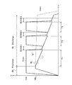
図4は、この実施の形態のNAND型フラッシュメモリが二値記憶を行う場合のデータのしきい値分布を示している。しきい値が負の状態がデータ“1”(消去状態)であり、しきい値が正の状態がデータ“0”(狭義の書き込み状態)である。データ“0”書き込みは、選択されたメモリセルの浮遊ゲートにチャネルからFNトンネリングにより電子を注入する動作として行われる。 FIG. 4 shows the threshold distribution of data when the NAND flash memory of this embodiment performs binary storage. A state with a negative threshold is data “1” (erased state), and a state with a positive threshold is data “0” (narrowly written state). Data “0” writing is performed as an operation of injecting electrons from the channel to the floating gate of the selected memory cell by FN tunneling.
具体的に1ページ分のデータ書き込みは、ビット線から各NANDセルの選択セルのチャネルに書き込みデータ“0”,“1”に対応して、Vss,Vdd−Vth(Vthは選択ゲートトランジスタSG1のしきい値)を転送し、選択されたワード線に書き込み電圧Vpgm(例えば20V)を与えて行われる。このとき、“0”データが与えられたメモリセルでは、浮遊ゲートとチャネル間に大きな電界がかかって、浮遊ゲートに電子が注入される(“0”書き込み)。“1”データが与えられたメモリセルでは、チャネルが容量カップリングにより電位上昇して、浮遊ゲートに電子注入が生じない(書き込み禁止)。 Specifically, for one page of data writing, Vss, Vdd-Vth (Vth is the value of the selection gate transistor SG1) corresponding to the write data “0”, “1” from the bit line to the channel of the selected cell of each NAND cell. Threshold value) is transferred, and a write voltage Vpgm (for example, 20 V) is applied to the selected word line. At this time, in the memory cell to which “0” data is applied, a large electric field is applied between the floating gate and the channel, and electrons are injected into the floating gate (“0” writing). In a memory cell to which “1” data is applied, the potential of the channel rises due to capacitive coupling, and electron injection does not occur in the floating gate (write inhibition).
データ書き込みは実際には、書き込みパルス電圧印加動作とその書き込み状態を確認する読み出し動作(書き込みベリファイ)を、1ページ分の書き込みデータが全て書き込まれるまで繰り返すことにより、行われる。 Data writing is actually performed by repeating a write pulse voltage application operation and a read operation (write verify) for confirming the write state until all the write data for one page is written.
データ消去は、選択ブロックの全ワード線に0Vを与え、選択ゲート線SGD,SGS、全ビット線BL及び共通ソース線CELSRCをフローティングとして、セルアレイが形成されたp型ウェルに消去電圧Vera(=20V)を与える。これにより、選択ブロックの全メモリセルの浮遊ゲートの電子がチャネルに放出され、しきい値が負の消去状態(データ“1”)が得られる。 In data erasing, 0 V is applied to all word lines of the selected block, the selection gate lines SGD, SGS, all bit lines BL, and the common source line CELSRC are floated, and the erase voltage Vera (= 20 V) is applied to the p-type well in which the cell array is formed. )give. As a result, the electrons of the floating gates of all the memory cells in the selected block are emitted to the channel, and an erased state (data “1”) having a negative threshold value is obtained.
次に、この実施の形態のフラッシュメモリの読み出し動作を説明する。図5は、一つのNANDセルユニットに着目して、読み出し時のバイアス条件を示している。読み出し時、ビット線BLは、電源電圧Vddより低い電圧VBLにプリチャージされる。その後、選択ワード線(図の場合、WL1)に0V、残りのワード線には、セルデータによらずセルがオンする、図4に示すようなパス電圧Vreadを与え、選択ゲート線SGD,SGSにもパス電圧Vreadを与える。このバイアス条件で、選択ワード線WL1に沿ったメモリセルのデータが“1”であれば、ビット線BLが放電され、“0”であれば、ビット線BLは放電されない。このセルデータに応じて異なるビット線放電状態を検出することにより、データを判定することができる。 Next, the read operation of the flash memory according to this embodiment will be described. FIG. 5 shows bias conditions at the time of reading, focusing on one NAND cell unit. At the time of reading, the bit line BL is precharged to a voltage VBL lower than the power supply voltage Vdd. Thereafter, 0 V is applied to the selected word line (WL1 in the figure), and the remaining word lines are supplied with a pass voltage Vread as shown in FIG. 4 which turns on the cells regardless of the cell data, and the selected gate lines SGD, SGS. Also, a pass voltage Vread is applied. Under this bias condition, if the data in the memory cell along the selected word line WL1 is “1”, the bit line BL is discharged, and if it is “0”, the bit line BL is not discharged. Data can be determined by detecting different bit line discharge states according to the cell data.
図6は、読み出し動作のシーケンス制御フローを示し、図7は図3のセンスユニットに着目して読み出し動作タイミングを示している。これらの図に示すように、この実施の形態では、ビット線放電動作の開始(タイミングt1)から、ビット線放電動作が続く間に、3回のデータセンスSENSE1(ステップS5)、SENSE2(ステップS8)、SENSE3(ステップS13)が行われる。そしてこれらのセンス結果に基づいて、選択セルのデータ状態が安定しているか否か、言い換えればデータマージン(しきい値マージン)が十分であるか否かの判定が行われる。以下、具体的に説明する。 FIG. 6 shows the sequence control flow of the read operation, and FIG. 7 shows the read operation timing by paying attention to the sense unit of FIG. As shown in these drawings, in this embodiment, the data sense SENSE1 (step S5) and SENSE2 (step S8) are performed three times during the bit line discharge operation from the start of the bit line discharge operation (timing t1). ), SENSE3 (step S13) is performed. Based on these sense results, it is determined whether or not the data state of the selected cell is stable, in other words, whether or not the data margin (threshold margin) is sufficient. This will be specifically described below.
読み出しのアドレス及びコマンドを受けると、コントローラ18はまず読み出しセットアップを行う(ステップS1)。読み出しセットアップでは、高電圧発生回路19が駆動されて、必要な内部高電圧が発生される。次にワード線WLやビット線BLの充電動作を開始する(ステップS2)。図5に示したように、選択ワード線には0Vが、非選択ワード線にはVreadが与えられる。選択ゲート線SGS,SGDには非選択ワード線と同時にVreadが与えられるが、但しビット線側の選択ゲート線SGDは、ビット線の放電開始までは、0Vを保つ。
Upon receiving the read address and command, the
ビット線プリチャージ動作は、図7に示すように、タイミングt0でトランジスタMN1のゲート端子CLAMPにVBL+Vth(VthはNMOSトランジスタのしきい値電圧)を、トランジスタMP3のゲート端子PREに“L”(=Vss)を与えることにより、行われる。センスノードNsenは、プリチャージ用トランジスタMP3により、Vddに、ビット線BLは、プリチャージ用トランジスタMP3及びクランプ用トランジスタMN1により、VBL(<Vdd)にそれぞれプリチャージされる。 As shown in FIG. 7, in the bit line precharge operation, VBL + Vth (Vth is the threshold voltage of the NMOS transistor) is applied to the gate terminal CLAMP of the transistor MN1 and “L” (= Vss) is performed. The sense node Nsen is precharged to Vdd by the precharging transistor MP3, and the bit line BL is precharged to VBL (<Vdd) by the precharging transistor MP3 and the clamping transistor MN1.
センスノードNsenのプリチャージ動作を継続しながら、タイミングt1でビット線プリチャージ動作を停止し、ビット線BLをVBLにプリチャージされたフローティング状態にする(ステップS3)。同時に選択ゲート線SGDにVreadを与えると、ビット線BLは、選択セルのデータに応じて放電される。図7に示すように、ビット線BLは、選択セルデータが“1”のときは、セル電流により放電されてレベル低下し(実線)、“0”のときは、リークによりわずかなレベル低下はあるものの、ほぼプリチャージ電圧VBLを保つ(破線)。図7では典型的なデータ“0”,“1”のビット線放電カーブを示しているが、実際には選択セルのデータ状態(しきい値状態)に応じて、種々の放電カーブを描く。 While continuing the precharge operation of the sense node Nsen, the bit line precharge operation is stopped at the timing t1, and the bit line BL is brought into a floating state precharged to VBL (step S3). At the same time, when Vread is applied to the selection gate line SGD, the bit line BL is discharged according to the data of the selected cell. As shown in FIG. 7, when the selected cell data is “1”, the bit line BL is discharged by the cell current and drops in level (solid line). Although it exists, the precharge voltage VBL is substantially maintained (broken line). FIG. 7 shows typical bit line discharge curves of data “0” and “1”, but actually, various discharge curves are drawn according to the data state (threshold state) of the selected cell.
ビット線放電開始から一定時間T1の待機(ステップS4)の後、第1回目のビット線データセンスSENSE1を行う(ステップS5)。即ち、図7に示すように、ゲートPREに“H”(=Vdd)を与えてプリチャージ用トランジスタMP3をオフにした後、クランプ用トランジスタMN1のゲートCLAMPにセンス用電圧Vsen+Vth(Vsen<VBL)を与える(タイミングt2−t3)。セルデータが“0”であれば、トランジスタMN1はオフを保ち、センスノードNsenは“H”レベルを保つ。セルデータが“1”でビット線BLが十分低レベルに放電されていれば、トランジスタNN1はオンして、センスノードNsenはビット線BLとの電荷分配により電圧が低下する。具体的にセンスノードNsenに比べてビット線BLの容量が十分に大きければ、この電荷分配によりセンスノードNsenはほぼビット電圧までレベル低下する。これによりビット線電圧は増幅されて、センスノードNsenに転送される。 After waiting for a predetermined time T1 from the start of the bit line discharge (step S4), the first bit line data sense SENSE1 is performed (step S5). That is, as shown in FIG. 7, after applying “H” (= Vdd) to the gate PRE to turn off the precharge transistor MP3, the sense voltage Vsen + Vth (Vsen <VBL) is applied to the gate CLAMP of the clamp transistor MN1. (Timing t2-t3). If the cell data is “0”, the transistor MN1 is kept off and the sense node Nsen is kept at the “H” level. If the cell data is “1” and the bit line BL is discharged to a sufficiently low level, the transistor NN1 is turned on, and the voltage at the sense node Nsen decreases due to charge sharing with the bit line BL. Specifically, if the capacitance of the bit line BL is sufficiently larger than the sense node Nsen, the level of the sense node Nsen is lowered to almost the bit voltage by this charge distribution. As a result, the bit line voltage is amplified and transferred to the sense node Nsen.
ビット線データセンスの結果は、ゲートBLCに“H”(=Vdd)を与えて転送トランジスタMN3をオンにすることにより、データラッチ31に転送されて保持される(タイミングt4)。実際にはデータラッチ31のクロックトインバータCI1,CI2は順次活性化されて、データ保持を行うが、図7のタイミング図ではその詳細動作は省略している。 The result of bit line data sensing is transferred to the data latch 31 and held by applying "H" (= Vdd) to the gate BLC and turning on the transfer transistor MN3 (timing t4). Actually, the clocked inverters CI1 and CI2 of the data latch 31 are sequentially activated to hold data, but the detailed operation is omitted in the timing chart of FIG.
データラッチ31にセンスデータを転送する間に、ビット線BLは再度フローティングにされて放電動作を続ける。またデータ転送後、センスノードNsenは改めてトランジスタMP3をオンにしてVddにプリチャージする(ステップS6)。このセンスノードNsenのプリチャージ動作の間、ゲートDTGに“H”(=Vdd)を与えて、転送トランジスタMN9をオンにして、データラッチ31のセンスデータを記憶ノードNRに転送する(タイミングt5)。 While the sense data is transferred to the data latch 31, the bit line BL is floated again and continues the discharge operation. After the data transfer, the sense node Nsen again turns on the transistor MP3 and precharges it to Vdd (step S6). During the precharge operation of the sense node Nsen, “H” (= Vdd) is applied to the gate DTG, the transfer transistor MN9 is turned on, and the sense data of the data latch 31 is transferred to the storage node NR (timing t5). .
そして、一定の時間T2の待機(ステップS7)の後、再度クランプ用トランジスタMN1のゲートCLAMPにセンス用電圧Vsen+Vthを与えて(タイミングt6−t7)、2回目のビット線データセンスSENSE2を行う(ステップS8)。このビット線データセンスの結果は、転送トランジスタMN3をオンにして、データラッチ31に転送し保持する(タイミングt8)。 Then, after waiting for a certain time T2 (step S7), the sense voltage Vsen + Vth is again applied to the gate CLAMP of the clamping transistor MN1 (timing t6-t7), and the second bit line data sense SENSE2 is performed (step S7). S8). The result of this bit line data sense is transferred to the data latch 31 with the transfer transistor MN3 turned on and held (timing t8).
データラッチ31にセンスデータを転送している間、ビット線放電動作を再開し、またセンスノードNsenのプリチャージを行う(ステップS9)。但し実際にセンスノードNsenのプリチャージ動作が開始される前に、1回目のセンスSENSE1の結果と、2回目のセンスSENSE2の結果のデータ比較を行う(ステップS10)。これら2回のセンスSENSE1,SENSE2の間でデータが反転している場合(即ち最初のセンス結果が“0”であり、次のセンス結果が“1”の場合)、コントローラはこれを検知してステータスレジスタ24に警告フラグをセットする(ステップS11)。 While the sense data is being transferred to the data latch 31, the bit line discharge operation is resumed and the sense node Nsen is precharged (step S9). However, before the precharge operation of the sense node Nsen is actually started, data comparison between the result of the first sense SENSE1 and the result of the second sense SENSE2 is performed (step S10). When data is inverted between these two senses SENSE1 and SENSE2 (that is, when the first sense result is “0” and the next sense result is “1”), the controller detects this. A warning flag is set in the status register 24 (step S11).
具体的に2回のセンス結果の比較は、図3に示すセンスユニット内のしきい値マージン判定回路33による各ビット線毎のしきい値マージン判定により行われる。即ち、DCHG=“H”(=Vdd)によりリセット用トランジスタMN10をオンにすると同時に、CHG=“L”(=Vss)によりチェック用トランジスタMP1をオンにして、センスノードNsenをVssに、ノードNDをVddにそれぞれ設定し(タイミングt9)。次いでREG=“H”(=Vdd)によりトランジスタMN8をオンにして、記憶ノードNRのデータをセンスノードNsenに転送する(タイミングt10)。 Specifically, the comparison of the sense results twice is performed by threshold margin determination for each bit line by the threshold margin determination circuit 33 in the sense unit shown in FIG. That is, the reset transistor MN10 is turned on by DCHG = “H” (= Vdd), and at the same time, the check transistor MP1 is turned on by CHG = “L” (= Vss), the sense node Nsen is set to Vss, and the node ND Are set to Vdd (timing t9). Next, the transistor MN8 is turned on by REG = “H” (= Vdd), and the data of the storage node NR is transferred to the sense node Nsen (timing t10).
前回のデータセンスSENSE1により得られた記憶ノードNRのデータと、今回のデータセンスSENSE2の結果によるデータノードN2のデータと異同によって、しきい値マージン判定回路33のトランジスタMN4,MN5のオンオフが決定され、従ってノードNDが放電されるか否かが決定される。このノードNDのレベル変化を受けて、検出信号線DETに信号が発生する。その詳細な動作説明は、後に行う。 On / off of the transistors MN4 and MN5 of the threshold margin determination circuit 33 is determined by the difference between the data of the storage node NR obtained by the previous data sense SENSE1 and the data of the data node N2 obtained by the result of the current data sense SENSE2. Thus, it is determined whether the node ND is discharged. In response to the level change of the node ND, a signal is generated on the detection signal line DET. The detailed operation will be described later.
一定の時間T3の待機(ステップS12)の間にセンスノードNsenを再度プリチャージしながら、タイミングt11で転送トランジスタMN9をオンにして、データラッチ31のセンスデータを記憶ノードNRに転送する。そして、センスノードNsenのプリチャージ動作を停止した後、クランプ用トランジスタMN1のゲートCLAMPにセンス用電圧Vsen+Vthを与えて(タイミングt12−t13)、3回目のビット線データセンスSENSE3を行う(ステップS13)。このビット線データセンスの結果は、転送トランジスタMN3をオンにして、データラッチ31に転送し保持する(タイミングt14)。 While waiting for a certain time T3 (step S12), the sense node Nsen is precharged again, the transfer transistor MN9 is turned on at timing t11, and the sense data of the data latch 31 is transferred to the storage node NR. Then, after stopping the precharge operation of the sense node Nsen, the sense voltage Vsen + Vth is applied to the gate CLAMP of the clamp transistor MN1 (timing t12-t13), and the third bit line data sense SENSE3 is performed (step S13). . The result of this bit line data sense is transferred to the data latch 31 with the transfer transistor MN3 turned on and held (timing t14).
2回目のデータセンスSENSE2の結果と、3回目のデータセンスSENSE3の結果の比較を行い(ステップS14)、コントローラはこれらのセンス結果が異なる場合に警告フラグをステータスレジスタ24にセットする(ステップS15)。
The result of the second data sense SENSE2 is compared with the result of the third data sense SENSE3 (step S14), and the controller sets a warning flag in the
以上の3回のデータセンスSENSE1,SENSE2,SENSE3のうち、第2回のデータセンスSENSE2のタイミングが従来の読み出し法でのそれと同じであるとする。この実施の形態では、この2回目のデータセンスSENSE2の結果を読み出しデータとしてページバッファ12に保存する(ステップS16)。具体的には、記憶ノードNRのデータをトランジスタMN8,MN3をオンにして、データラッチ31に書き戻す。そして、ワード線及びビット線を放電して(ステップS17)、読み出し動作を終了する。この後、外部から読み出しイネーブル信号を入力することにより、ページバッファ12が保持するページデータは、1バイトずつシリアル出力される。
Of the above three data senses SENSE1, SENSE2 and SENSE3, the timing of the second data sense SENSE2 is assumed to be the same as that in the conventional read method. In this embodiment, the result of the second data sense SENSE2 is stored in the
図8は、以上のデータセンス動作を、ビット線BLとセンスノードNsenのみに着目して示している。クランプ用トランジスタMN1に与えられるセンス用電圧Vsenは、図8に示すように、一定のビット線放電動作の後のビット線BLの“H”レベル(データ“0”)と“L”レベル(データ“1”)の間に設定される。1回目のデータセンスSENSE1と2回目のデータセンスSENSE2を比べると、前者の方が“1”データに対するマージンが小さい読み出し動作となる。つまり、1回目のデータセンスSENSE1では、“1”データセルのしきい値が十分に低くなければ、センス結果が“0”となる可能性がある。一方、2回目のデータセンスSENSE2と3回目のデータセンスSENSE3を比べると、後者の方が0”データに対するマージンが小さい。従って、3回目のデータセンスSENSE3では、“0”データセルのしきい値が十分に高くなく、リークが大きいと、センス結果が“1”となる可能性がある。 FIG. 8 shows the above data sensing operation focusing on only the bit line BL and the sense node Nsen. As shown in FIG. 8, the sense voltage Vsen applied to the clamping transistor MN1 is set to the “H” level (data “0”) and “L” level (data) of the bit line BL after a constant bit line discharge operation. It is set during “1”). Comparing the first data sense SENSE1 and the second data sense SENSE2, the former is a read operation with a smaller margin for “1” data. That is, in the first data sense SENSE1, if the threshold value of the “1” data cell is not sufficiently low, the sense result may be “0”. On the other hand, when the second data sense SENSE2 is compared with the third data sense SENSE3, the latter has a smaller margin for 0 ”data. Therefore, in the third data sense SENSE3, the threshold value of the“ 0 ”data cell If the value is not sufficiently high and the leak is large, the sense result may be “1”.
即ち、選択セルのしきい値マージンが十分に大きい場合、言い換えれば“0”データセルのリークが十分に小さくかつ、“1”データセルの放電が十分に大きい場合には、3回のセンス結果は同じになるが、“0”,“1”データのいずれかのマージンが小さいと、3回のデータセンスのどこかで、センス結果が“0”から“1”に変化する。より具体的に言えば、“1”データセルの放電カープが緩い場合には、1回目のセンスSENSE1で“0”、2回目のセンスSENSE2で“1”になる可能性がある。一方、“0”データセルのリークが大きい場合には、2回目のセンスSENSE2では“0”であるが、3回目のセンスSENSE3で“1”(誤データ)になる可能性がある。 That is, when the threshold margin of the selected cell is sufficiently large, in other words, when the leak of the “0” data cell is sufficiently small and the discharge of the “1” data cell is sufficiently large, the sense result of 3 times However, if the margin of either “0” or “1” data is small, the sense result changes from “0” to “1” somewhere in the three data senses. More specifically, when the discharge carp of the “1” data cell is loose, there is a possibility that the first sense SENSE1 is “0” and the second sense SENSE2 is “1”. On the other hand, if the leak of the “0” data cell is large, it is “0” in the second sense SENSE2, but may be “1” (incorrect data) in the third sense SENSE3.
この様な引き続く2回のデータセンスの間でのデータ反転(論理反転)を判定するのが、上述のステップS10及びS14である。このセンスデータの変化によるしきい値マージン判定の動作を、具体的に図9〜図11を参照して説明する。図9〜図11は、図3のセンスユニットのしきい値マージン判定動作時の状態を示している。 It is the above-described steps S10 and S14 that determine data inversion (logical inversion) between two subsequent data senses. The threshold margin determination operation based on the change in the sense data will be specifically described with reference to FIGS. 9 to 11 show states at the time of threshold margin determination operation of the sense unit of FIG.
図9は、先行するデータセンスによるデータが“0”(記憶ノードNR=“H”)であり、続くデータセンスによるデータが“0”(データノードN1=“H”)の場合である。センスノードNsenは、トランジスタMN10をオンにすることにより、予めVssにリセットされる。この状態で、トランジスタMN8のゲートREGに“H”レベルを与えると、記憶ノードNRが“H”であるから、トランジスタMN7,MN8が共にオンして、破線で示すように、VddがセンスノードNsenを介して、トランジスタMN5のゲートに与えられる。これにより、トランジスタMN5がオンする。しかしこのとき、データノードN2(=“L”)により駆動されるトランジスタMN4はオフであり、プリチャージされたノードNDは、放電されることなく、“H”レベルを保つ。 FIG. 9 shows a case where the data by the preceding data sense is “0” (storage node NR = “H”) and the data by the subsequent data sense is “0” (data node N1 = “H”). The sense node Nsen is reset to Vss in advance by turning on the transistor MN10. In this state, when the “H” level is applied to the gate REG of the transistor MN8, the storage node NR is “H”, so that both the transistors MN7 and MN8 are turned on and Vdd is sense node Nsen as indicated by the broken line. Is provided to the gate of the transistor MN5. As a result, the transistor MN5 is turned on. However, at this time, the transistor MN4 driven by the data node N2 (= “L”) is off, and the precharged node ND maintains the “H” level without being discharged.
図10は、先行するデータセンスによるデータが“0”(記憶ノードNR=“H”)であり、続くデータセンスによるデータが“1”(データノードN1=“L”)の場合である。このとき、トランジスタMN8のゲートREGに“H”レベルを与えると、トランジスタMN7,MN8が共にオンして、破線で示すように、VddがセンスノードNsenを介して、トランジスタMN5のゲートに与えられ、トランジスタMN5がオンする。また、データノードN2の“H”により制御されてトランジスタMN4もオンする。この結果、ノードNDは放電されて、“L”レベルになる。 FIG. 10 shows a case where the data by the preceding data sense is “0” (storage node NR = “H”) and the data by the subsequent data sense is “1” (data node N1 = “L”). At this time, if the “H” level is applied to the gate REG of the transistor MN8, the transistors MN7 and MN8 are both turned on, and Vdd is applied to the gate of the transistor MN5 via the sense node Nsen as indicated by the broken line. The transistor MN5 is turned on. Also, the transistor MN4 is turned on under the control of “H” of the data node N2. As a result, the node ND is discharged to the “L” level.
図11は、先行するデータセンスによるデータが“1”(記憶ノードNR=“L”)であり、続くデータセンスによるデータが“1”(データノードN1=“L”)の場合である。このとき、トランジスタMN7がオフであるから、トランジスタMN8をオンにしても、VddはトランジスタMN5のゲートに転送されない。従って、トランジスタMN4はオンするが、トランジスタMN5はオフを保ち、プリチャージされたノードNDは放電されずに“H”レベルを保つ。 FIG. 11 shows a case where the data by the preceding data sense is “1” (storage node NR = “L”) and the data by the subsequent data sense is “1” (data node N1 = “L”). At this time, since the transistor MN7 is off, even if the transistor MN8 is turned on, Vdd is not transferred to the gate of the transistor MN5. Accordingly, the transistor MN4 is turned on, but the transistor MN5 is kept off, and the precharged node ND is not discharged but kept at the “H” level.
以上のようにして、3回のビット線データセンスの間にセンスデータの“0”から“1”への変化があると、センスユニットのしきい値マージン判定回路33のノードNDはレベル低下する。これにより、トランジスタMP2がオンして、共通信号線DETに“H”レベル信号が発生する。即ち1ページ分の読み出しデータのなかに一つでもしきい値マージンが低いものがあると、共通信号線DETに警告信号が出力される。図1のDETモニター回路17はこの信号線DETをモニターして、データマージンが低いときに警告信号“WARN”を発生し、コントローラ18に送る。コントローラ18はこれを受けて、ステータスレジスタ24に警告信号をセットする。
As described above, if the sense data changes from “0” to “1” during the three bit line data senses, the level of the node ND of the threshold margin judgment circuit 33 of the sense unit is lowered. . As a result, the transistor MP2 is turned on, and an “H” level signal is generated on the common signal line DET. That is, if even one of the read data for one page has a low threshold margin, a warning signal is output to the common signal line DET. The
なおしきい値マージン判定回路33は、前述のように書き込み或いは消去時のベリファイ判定回路としても用いられる。例えば書き込み時は、CPU26から書き込みコマンド及びアドレスが入力される。これを受けて内部コントローラ18の制御により、書き込み電圧印加動作とベリファイ読み出し動作からなる書き込みサイクルが、1ページの全“0”書き込みビットの書き込みが完了するまで繰り返される。書き込みが完了すると、ベリファイ判定回路33が“Pass”フラグを出力し、コントローラ18はこれを受けて、書き込みシーケンスを終了する。
The threshold margin determining circuit 33 is also used as a verify determining circuit at the time of writing or erasing as described above. For example, at the time of writing, a write command and an address are input from the
規定回数の書き込みとベリファイを繰り返しても書き込みがパスしないときは、コントローラ18は、ステータスレジスタ24に“Fail”フラグをセットして、書き込みシーケンスを終了する。CPU26は、このステータスレジスタ24の情報に基づいて、書き込みのフェイル/パスを知ることができる。
If the writing does not pass even if the writing and verification are repeated a prescribed number of times, the
以上のようにこの実施の形態の読み出し方式によれば、読み出しデータのマージン判定が可能になる。この様な読み出し方式を適用すれば、ステータスレジスタ24の情報に基づいて、読み出したデータにビットエラーがある可能性について判断が可能である。即ち、ステータスレジスタ24に警告信号がセットされているときには、読み出しデータにエラービットがある可能性が高く、その場合にはエラーチェックと訂正を行い、警告信号が出力されていない場合には、エラーチェックと訂正を行わない、という制御が可能になる。
As described above, according to the reading method of this embodiment, it is possible to determine the margin of read data. If such a reading method is applied, it is possible to determine whether or not there is a bit error in the read data based on the information in the
具体的に、上述した読み出し方式をページコピー動作に適用した例を次に説明する。図12は、コントローラ18により制御されるページコピーの動作フローを示している。外部からコピー元のページアドレスとコマンドを入力すると、上述した読み出し方式で、コピー元ページのデータをページバッファ12に読み出す(ステップS21)。この読み出し動作後、内部コントローラ18は、ステータスレジスタ24に警告フラグがセットされているかどうかのチェックを行う(ステップS22)。警告フラグが出力されていない場合には、外部からコピー先アドレスを入力することにより、コントローラ18は、ページバッファ12に読み出されたデータをそのまま、コピー先ページに書き込む動作を実行する(ステップS27)。
Specifically, an example in which the above-described reading method is applied to a page copy operation will be described next. FIG. 12 shows an operation flow of page copy controlled by the
警告フラグがセットされている場合には、ECC計算フェーズに移る。即ち、コントローラ18の制御により、ページバッファ12の読み出しデータを1バイトずつシリアル転送して、ECC回路23に入力し、エラービットがあるかどうかを検出する(ステップS23)。前述のように、しきい値マージン判定の結果である警告フラグは、しきい値マージンが十分ではないことを示すものであり、必ずしも読み出しデータにエラーがあるとは限らない。エラービットが検出されなければ、ページバッファ12の読み出しデータをそのまま、コピー先ページに書き込む(ステップS27)。
If the warning flag is set, the process proceeds to the ECC calculation phase. That is, under the control of the
エラービットが検出されたときは、ECC回路23によるエラー訂正(ステップS25)、訂正されたデータのページバッファ12への書き戻しが行われる(ステップS26)。このデータ書き戻しは、1ページ全体でもよいが、訂正ビットを含む1バイト分のみをオーバーライトしてもよい。そして、ページバッファ12に保存された訂正されたページデータがコピー先ページに書き込まれる(ステップS27)。
When an error bit is detected, error correction by the ECC circuit 23 (step S25) and correction data is written back to the page buffer 12 (step S26). This data write-back may be performed for the entire page, or only one byte including the correction bit may be overwritten. Then, the corrected page data stored in the
以上のようにこの実施の形態によると、ページコピー動作において、エラー出現の可能性が高い場合のみ、エラーチェックと訂正を実行するという制御が行われる。前述のように1ページデータのエラーチェック及び訂正のためには、読み出しデータを1バイトずつECC回路に入力することが必要であり、長い時間を必要とする。この実施の形態によると、エラー出現の可能性が低いときにはその様なエラーチェック及び訂正の動作を省くことができ、これにより、高速のページコピーが可能になる。 As described above, according to this embodiment, in the page copy operation, control for executing error check and correction is performed only when there is a high possibility of error occurrence. As described above, in order to perform error check and correction of one page data, it is necessary to input read data byte by byte to the ECC circuit, which requires a long time. According to this embodiment, when the possibility of error occurrence is low, such error check and correction operations can be omitted, thereby enabling high-speed page copying.
[実施の形態2]
図1に示した実施の形態では、ECC回路23がメモリチップ10の内部に搭載されている。この場合には、ページコピーの読み出しデータに対するECC計算やエラー訂正を行うか否かは、内部コントローラ18がステータスレジスタ21の情報を参照して自ら判断する。
[Embodiment 2]
In the embodiment shown in FIG. 1, the
これに対して、図13に示すように、ECC回路23をメモリチップ10の外に配置する場合もある。この場合のページコピー動作は、次のようになる。
On the other hand, as shown in FIG. 13, the
コピー元ページのデータをページバッファ12に読み出す動作は、上記実施の形態と同様である。ページバッファ12において、読み出し時のその読み出しデータのしきい値マージンが十分であるか否かの判定がなされる。しきい値マージンが小さい場合には、モニター回路17から発生される警告フラグ“WARN”が、コントローラ18を介することなく、ステータスレジスタ24に直接セットされる。
The operation of reading the copy source page data to the
外部CPU26は、ECC回路23の活性化に先立って、ステータスレジスタ24の情報に基づいてECC計算が必要か否かを判定する。必要がない場合には、CPU26がコピー先ページアドレスを入力することにより、ページバッファ12が保持する読み出しデータをそのままコピー先ページに書き込む動作が行われる。その書き込みシーケンス制御は、先の実施の形態と同様、内部コントローラ18により行われる。
Prior to the activation of the
ECC計算が必要である場合には、CPU26は読み出しイネーブル信号をメモリチップ10に供給する。これにより、ページバッファ12が保持するデータはシリアル出力されて、ECC回路23に入力され、ECC計算及びエラー訂正が行われる。そして訂正データをページバッファ12にロードした後、コピー先ページへの書き込みが行われる。訂正データのロードは、先の実施の形態と同様に、訂正ビットを含む1バイトのみでよい。
When ECC calculation is necessary, the
この実施の形態によっても、先の実施の形態と同様の効果が得られる。 Also in this embodiment, the same effect as the previous embodiment can be obtained.
[実施の形態3]
次に、上記各実施の形態による不揮発性半導体記憶装置或いはメモリシステムを搭載した電子カードと、その電子カードを用いた電子装置の実施の形態を説明する。
[Embodiment 3]
Next, an embodiment of an electronic card on which the nonvolatile semiconductor memory device or memory system according to each of the above embodiments is mounted and an electronic device using the electronic card will be described.
図14は、この実施の形態による電子カードと、この電子カードを用いた電子装置の構成を示す。ここでは電子装置は、携帯電子機器の一例としてのディジタルスチルカメラ101を示す。電子カードは、ディジタルスチルカメラ101の記録媒体として用いられるメモリカード61である。メモリカード61は、先の各実施の形態で説明した不揮発性半導体装置或いはメモリシステムが集積化され封止されたICパッケージPK1を有する。
FIG. 14 shows the configuration of an electronic card according to this embodiment and an electronic device using this electronic card. Here, the electronic device represents a digital
ディジタルスチルカメラ101のケースには、カードスロット102と、このカードスロット102に接続された、図示しない回路基板が収納されている。メモリカード61は、カードスロット102に取り外し可能に装着される。メモリカード61は、カードスロット102に装着されると、回路基板上の電気回路に電気的に接続される。
The case of the digital
電子カードが例えば、非接触型のICカードである場合、カードスロット102に収納し、或いは近づけることによって、回路基板上の電気回路に無線信号により接続される。
When the electronic card is, for example, a non-contact type IC card, the electronic card is connected to the electric circuit on the circuit board by a radio signal by being stored in or close to the
図15は、ディジタルスチルカメラの基本的な構成を示す。被写体からの光は、レンズ103により集光されて撮像装置104に入力される。撮像装置104は例えばCMOSイメージセンサであり、入力された光を光電変換し、アナログ信号を出力する。このアナログ信号は、アナログ増幅器(AMP)により増幅された後、A/Dコンバータによりディジタル変換される。変換された信号は、カメラ信号処理回路105に入力され、例えば自動露出制御(AE)、自動ホワイトバランス制御(AWB)、及び色分離処理を行った後、輝度信号と色差信号に変換される。
FIG. 15 shows a basic configuration of a digital still camera. Light from the subject is collected by the
画像をモニターする場合、カメラ信号処理回路105から出力された信号はビデオ信号処理回路106に入力され、ビデオ信号に変換される。ビデオ信号の方式としては、例えばNTSC(National Television System Committee)を挙げることができる。ビデオ信号は、表示信号処理回路107を介して、ディジタルスチルカメラ101に取り付けられた表示部108に出力される。表示部108は例えば液晶モニターである。
When monitoring an image, the signal output from the camera
ビデオ信号は、ビデオドライバ109を介してビデオ出力端子110に与えられる。ディジタルスチルカメラ101により撮像された画像は、ビデオ出力端子110を介して、例えばテレビジョン等の画像機器に出力することができる。これにより、撮像した画像を表示部108以外でも表示することができる。撮像装置104、アナログ増幅器(AMP)、A/Dコンバータ(A/D)、カメラ信号処理回路105は、マイクロコンピュータ111により制御される。
The video signal is given to the
画像をキャプチャする場合、操作ボタン例えばシャッタボタン112を操作者が押す。これにより、マイクロコンピュータ111が、メモリコントローラ113を制御し、カメラ信号処理回路105から出力された信号がフレーム画像としてビデオメモリ114に書き込まれる。ビデオメモリ114に書き込まれたフレーム画像は、圧縮/伸張処理回路115により、所定の圧縮フォーマットに基づいて圧縮され、カードインタフェース116を介してカードスロット102に装着されているメモリカード61に記録される。
When capturing an image, the operator presses an operation button such as the
記録した画像を再生する場合、メモリカード61に記録されている画像を、カードインタフェース116を介して読み出し、圧縮/伸張処理回路115により伸張した後、ビデオメモリ114に書き込む。書き込まれた画像はビデオ信号処理回路106に入力され、画像をモニターする場合と同様に、表示部108や画像機器に映し出される。
When reproducing the recorded image, the image recorded on the
なおこの構成では、回路基板100上に、カードスロット102、撮像装置104、アナログ増幅器(AMP)、A/Dコンバータ(A/D)、カメラ信号処理回路105、ビデオ信号処理回路106、メモリコントローラ113、ビデオメモリ114、圧縮/伸張処理回路115、及びカードインタフェース116が実装される。
In this configuration, the
但しカードスロット102については、回路基板100上に実装される必要はなく、コネクタケーブル等により回路基板100に接続されるようにしてもよい。
However, the
回路基板100上には更に、電源回路117が実装される。電源回路117は、外部電源、或いは電池からの電源の供給を受け、ディジタルスチルカメラの内部で使用する内部電源電圧を発生する。電源回路117として、DC−DCコンバータを用いてもよい。内部電源電圧は、上述した各回路に供給される他、ストロボ118、表示部108にも供給される。
A
以上のようにこの実施の形態の電子カードは、ディジタルスチルカメラ等の携帯電子機器に用いることが可能である。更にこの電子カードは、携帯電子機器だけでなく、図16A−16Jに示すような他の各種電子機器に適用することができる。即ち、図16Aに示すビデオカメラ、図16Bに示すテレビジョン、図16Cに示すオーディオ機器、図16Dに示すゲーム機器、図16Eに示す電子楽器、図16Fに示す携帯電話、図16Gに示すパーソナルコンピュータ、図16Hに示すパーソナルディジタルアシスタント(PDA)、図16Iに示すヴォイスレコーダ、図16Jに示すPCカード等に、上記電子カードを用いることができる。 As described above, the electronic card of this embodiment can be used for portable electronic devices such as a digital still camera. Furthermore, this electronic card can be applied not only to portable electronic devices but also to various other electronic devices as shown in FIGS. 16A-16J. 16A, a television set shown in FIG. 16B, an audio device shown in FIG. 16C, a game machine shown in FIG. 16D, an electronic musical instrument shown in FIG. 16E, a mobile phone shown in FIG. 16F, and a personal computer shown in FIG. The electronic card can be used for a personal digital assistant (PDA) shown in FIG. 16H, a voice recorder shown in FIG. 16I, a PC card shown in FIG. 16J, and the like.
10…メモリチップ、11…セルアレイ、11a…ノーマルデータ領域、11b…冗長領域、12…センスアンプ回路(ページバッファ)、13…カラム選択ゲート回路、14…データバス、15…ロウデコーダ、16…カラムデコーダ、17…DETモニター回路、18…コントローラ、19…高電圧発生回路、20…コマンドデコーダ、21…アドレスバッファ、22…データバッファ、23…ECC回路、24…ステータスレジスタ、25…バッファメモリ、26…CPU、31…データラッチ、32…データ記憶回路、33…しきい値マージン判定回路、MC0−MC15…メモリセル、SG1,SG2…選択ゲートトランジスタ、WL0−WL15…ワード線、BL0−BLn−1…ビット線、SGD,SGS…選択ゲート線、CELSRC…共通ソース線。
DESCRIPTION OF
Claims (3)
前記セルアレイのビット線の電圧変化を検出することによりそのビット線に接続された選択メモリセルのデータを読み出すセンスアンプ回路と、
前記センスアンプ回路の読み出しデータについてエラーチェックと訂正を行うように制御されるECC回路と
を備え、
前記センスアンプ回路は、
前記セルアレイのビット線とセンスノードの間を選択的に接続して、ビット線電圧のクランプ動作とビット線電圧をセンスノードに転送する動作を行う第1のトランジスタと、
前記センスノードに接続されてセンスノードとビット線のプリチャージを行う第2のトランジスタと、
前記センスノードに転送されたビット線電圧を検出して読み出しデータをラッチするデータラッチと、
前記データラッチから転送された読み出しデータを一時保持するデータ記憶回路と、
前記データ記憶回路が保持する第1の読み出しデータと、この第1の読み出しデータに遅れて読み出されて前記データラッチが保持する第2の読み出しデータとを比較し、データ反転を検出した場合に警告信号を出力するしきい値マージン判定回路と
を有すると共に、前記選択メモリセルのデータに応じて前記ビット線の電圧が変化する期間内の複数タイミングでデータ読み出しを行い、連続する2回のデータ読み出しによる読み出しデータを比較して前記選択メモリセルのしきい値マージンを判定するように構成され、
前記ECC回路は、前記警告信号が出力された場合のみ読み出しデータについてエラーチェックと訂正を行う
ことを特徴とする不揮発性半導体記憶装置。 A cell array in which electrically rewritable nonvolatile memory cells are arranged;
A sense amplifier circuit that reads data of a selected memory cell connected to the bit line by detecting a voltage change of the bit line of the cell array;
An ECC circuit controlled to perform error check and correction on the read data of the sense amplifier circuit , and
The sense amplifier circuit is
A first transistor that selectively connects a bit line and a sense node of the cell array to perform a clamping operation of the bit line voltage and an operation of transferring the bit line voltage to the sense node;
A second transistor connected to the sense node for precharging the sense node and the bit line;
A data latch for detecting the bit line voltage transferred to the sense node and latching read data;
A data storage circuit for temporarily holding read data transferred from the data latch;
When the first read data held by the data storage circuit is compared with the second read data read after the first read data and held by the data latch, and data inversion is detected Threshold margin judgment circuit that outputs warning signal and
And reading data at a plurality of timings within a period in which the voltage of the bit line changes according to the data of the selected memory cell, and comparing the read data by two successive data readings Configured to determine the threshold margin of
The nonvolatile semiconductor memory device , wherein the ECC circuit performs error check and correction on read data only when the warning signal is output .
前記セルアレイのビット線の電圧変化を検出することによりそのビット線に接続された選択メモリセルのデータを読み出すセンスアンプ回路と、
前記センスアンプ回路の読み出しデータについてエラーチェックと訂正を行うように制御されるECC回路と
を備え、
前記センスアンプ回路は、
前記セルアレイのビット線とセンスノードの間を選択的に接続して、ビット線電圧のクランプ動作とビット線電圧をセンスノードに転送する動作を行う第1のトランジスタと、
前記センスノードに接続されてセンスノードとビット線のプリチャージを行う第2のトランジスタと、
前記センスノードに転送されたビット線電圧を検出して読み出しデータをラッチするデータラッチと、
前記データラッチから転送された読み出しデータを一時保持するデータ記憶回路と、
前記データ記憶回路が保持する第1の読み出しデータと、この第1の読み出しデータに遅れて読み出されて前記データラッチが保持する第2の読み出しデータとを比較し、データ反転を検出した場合に警告信号を出力するしきい値マージン判定回路と
を有すると共に、前記選択メモリセルのデータに応じて前記ビット線の電圧が変化する期間内の複数タイミングでデータ読み出しを行い、連続する2回のデータ読み出しによる読み出しデータを比較して前記選択メモリセルのしきい値マージンを判定するように構成され、
前記セルアレイのあるページのデータを読み出して、他のページに書き込むページコピー機能を有し、
前記ECC回路は、コピー元ページの読み出しデータについて前記警告信号が出力された場合のみエラーチェックと訂正を行うように制御される
ことを特徴とする不揮発性半導体記憶装置。 A cell array in which electrically rewritable nonvolatile memory cells are arranged;
A sense amplifier circuit that reads data of a selected memory cell connected to the bit line by detecting a voltage change of the bit line of the cell array;
An ECC circuit controlled to perform error check and correction on the read data of the sense amplifier circuit;
With
The sense amplifier circuit is
A first transistor that selectively connects a bit line and a sense node of the cell array to perform a clamping operation of the bit line voltage and an operation of transferring the bit line voltage to the sense node;
A second transistor connected to the sense node for precharging the sense node and the bit line;
A data latch for detecting the bit line voltage transferred to the sense node and latching read data;
A data storage circuit for temporarily holding read data transferred from the data latch;
When the first read data held by the data storage circuit is compared with the second read data read after the first read data and held by the data latch, and data inversion is detected Threshold margin judgment circuit that outputs warning signal and
And reading data at a plurality of timings within a period in which the voltage of the bit line changes according to the data of the selected memory cell, and comparing the read data by two successive data readings Configured to determine the threshold margin of
Read page data in the cell array and have a page copy function to write to other pages;
The ECC circuit, copies of the original pages of read data you wherein controlled Ru <br/> it to make a correction and error check only when the warning signal is output nonvolatile semiconductor memory device.
ことを特徴とする請求項1又は2記載の不揮発性半導体記憶装置。 The cell array is formed by arranging a plurality of NAND cell units, and each NAND cell unit has a plurality of series-connected memory cells each having a control gate connected to a different word line and one end connected to a bit line. A NAND cell unit having a first select gate transistor for connecting to the common source line and a second select gate transistor for connecting the other end to the common source line and sharing one word line in the bit line direction. the nonvolatile semiconductor memory device according to claim 1, wherein it has a plurality of blocks defined as.
Priority Applications (4)
| Application Number | Priority Date | Filing Date | Title |
|---|---|---|---|
| JP2004002041A JP4322686B2 (en) | 2004-01-07 | 2004-01-07 | Nonvolatile semiconductor memory device |
| US10/856,851 US6982904B2 (en) | 2004-01-07 | 2004-06-01 | Non-volatile semiconductor memory device and electric device with the same |
| TW093141820A TWI256052B (en) | 2004-01-07 | 2004-12-31 | Non-volatile semiconductor memory device |
| KR1020050001054A KR100690476B1 (en) | 2004-01-07 | 2005-01-06 | Nonvolatile semiconductor memory |
Applications Claiming Priority (1)
| Application Number | Priority Date | Filing Date | Title |
|---|---|---|---|
| JP2004002041A JP4322686B2 (en) | 2004-01-07 | 2004-01-07 | Nonvolatile semiconductor memory device |
Publications (2)
| Publication Number | Publication Date |
|---|---|
| JP2005196871A JP2005196871A (en) | 2005-07-21 |
| JP4322686B2 true JP4322686B2 (en) | 2009-09-02 |
Family
ID=34709025
Family Applications (1)
| Application Number | Title | Priority Date | Filing Date |
|---|---|---|---|
| JP2004002041A Expired - Fee Related JP4322686B2 (en) | 2004-01-07 | 2004-01-07 | Nonvolatile semiconductor memory device |
Country Status (4)
| Country | Link |
|---|---|
| US (1) | US6982904B2 (en) |
| JP (1) | JP4322686B2 (en) |
| KR (1) | KR100690476B1 (en) |
| TW (1) | TWI256052B (en) |
Families Citing this family (51)
| Publication number | Priority date | Publication date | Assignee | Title |
|---|---|---|---|---|
| JP3631463B2 (en) | 2001-12-27 | 2005-03-23 | 株式会社東芝 | Nonvolatile semiconductor memory device |
| JP3977799B2 (en) * | 2003-12-09 | 2007-09-19 | 株式会社東芝 | Nonvolatile semiconductor memory device |
| US7453840B1 (en) | 2003-06-30 | 2008-11-18 | Cisco Systems, Inc. | Containment of rogue systems in wireless network environments |
| JP2005092969A (en) * | 2003-09-16 | 2005-04-07 | Renesas Technology Corp | Nonvolatile semiconductor memory |
| JP2006048783A (en) * | 2004-08-02 | 2006-02-16 | Renesas Technology Corp | Nonvolatile memory and memory card |
| JP4271168B2 (en) * | 2004-08-13 | 2009-06-03 | 株式会社東芝 | Semiconductor memory device |
| US7805140B2 (en) * | 2005-02-18 | 2010-09-28 | Cisco Technology, Inc. | Pre-emptive roaming mechanism allowing for enhanced QoS in wireless network environments |
| KR100618051B1 (en) * | 2005-09-08 | 2006-08-30 | 삼성전자주식회사 | Apparatus and method for detecting voltage glitches |
| KR100737914B1 (en) * | 2005-11-10 | 2007-07-10 | 삼성전자주식회사 | Page buffer and driving method thereof, and nonvolatile memory device having the same |
| US7489546B2 (en) * | 2005-12-20 | 2009-02-10 | Micron Technology, Inc. | NAND architecture memory devices and operation |
| KR100724339B1 (en) * | 2006-01-25 | 2007-06-04 | 삼성전자주식회사 | A three-level nonvolatile semiconductor memory device having a fast first page read speed and a driving method thereof |
| US7436708B2 (en) * | 2006-03-01 | 2008-10-14 | Micron Technology, Inc. | NAND memory device column charging |
| US7450422B2 (en) | 2006-05-11 | 2008-11-11 | Micron Technology, Inc. | NAND architecture memory devices and operation |
| KR100735758B1 (en) | 2006-06-29 | 2007-07-06 | 삼성전자주식회사 | Majority judgment circuits, data bus inversion circuits, and semiconductor devices. |
| US7688102B2 (en) | 2006-06-29 | 2010-03-30 | Samsung Electronics Co., Ltd. | Majority voter circuits and semiconductor devices including the same |
| US7551467B2 (en) * | 2006-08-04 | 2009-06-23 | Micron Technology, Inc. | Memory device architectures and operation |
| KR100794664B1 (en) * | 2006-09-01 | 2008-01-14 | 삼성전자주식회사 | Flash memory device and its refresh method |
| JP4791943B2 (en) * | 2006-11-30 | 2011-10-12 | 東芝マイクロエレクトロニクス株式会社 | Semiconductor device |
| US20080158986A1 (en) * | 2006-12-29 | 2008-07-03 | Daniel Elmhurst | Flash memory and associated methods |
| US8391061B2 (en) | 2006-12-29 | 2013-03-05 | Intel Corporation | Flash memory and associated methods |
| JP5145720B2 (en) * | 2007-01-31 | 2013-02-20 | 富士通セミコンダクター株式会社 | Charge loss repair method and semiconductor memory device |
| JP5283845B2 (en) | 2007-02-07 | 2013-09-04 | 株式会社メガチップス | Bit error prevention method and information processing apparatus |
| KR100871700B1 (en) * | 2007-02-13 | 2008-12-08 | 삼성전자주식회사 | Error Data Correction Method Due to Charge Loss in Nonvolatile Memory Devices |
| US7719901B2 (en) * | 2007-06-05 | 2010-05-18 | Micron Technology, Inc. | Solid state memory utilizing analog communication of data values |
| US7545678B2 (en) * | 2007-06-29 | 2009-06-09 | Sandisk Corporation | Non-volatile storage with source bias all bit line sensing |
| US9582417B2 (en) * | 2007-08-30 | 2017-02-28 | Virident Systems, Llc | Memory apparatus and methods thereof for preventing read errors on weak pages in a non-volatile memory system |
| KR101248942B1 (en) * | 2007-10-17 | 2013-03-29 | 삼성전자주식회사 | Non-volatile memory device |
| US7701761B2 (en) * | 2007-12-20 | 2010-04-20 | Sandisk Corporation | Read, verify word line reference voltage to track source level |
| KR101466698B1 (en) * | 2008-02-19 | 2014-11-28 | 삼성전자주식회사 | How to read memory devices and memory data |
| US7957197B2 (en) * | 2008-05-28 | 2011-06-07 | Sandisk Corporation | Nonvolatile memory with a current sense amplifier having a precharge circuit and a transfer gate coupled to a sense node |
| US8406048B2 (en) * | 2008-08-08 | 2013-03-26 | Marvell World Trade Ltd. | Accessing memory using fractional reference voltages |
| JP5193830B2 (en) | 2008-12-03 | 2013-05-08 | 株式会社東芝 | Nonvolatile semiconductor memory |
| KR20100093885A (en) | 2009-02-17 | 2010-08-26 | 삼성전자주식회사 | Nonvolatile memory device, operating method thereof and memory system including the same |
| JP2011258289A (en) * | 2010-06-10 | 2011-12-22 | Toshiba Corp | Method for detecting threshold value of memory cell |
| US8599609B2 (en) * | 2010-12-22 | 2013-12-03 | HGST Netherlands B.V. | Data management in flash memory using probability of charge disturbances |
| US9147454B2 (en) | 2013-01-14 | 2015-09-29 | Qualcomm Incorporated | Magnetic tunneling junction non-volatile register with feedback for robust read and write operations |
| JP2014157650A (en) * | 2013-02-18 | 2014-08-28 | Toshiba Corp | Semiconductor memory device |
| US9496023B2 (en) | 2014-06-05 | 2016-11-15 | Micron Technology, Inc. | Comparison operations on logical representations of values in memory |
| KR102258905B1 (en) * | 2015-07-02 | 2021-05-31 | 에스케이하이닉스 주식회사 | Semiconductor device and operating method thereof |
| JP6370444B1 (en) * | 2017-06-20 | 2018-08-08 | ウィンボンド エレクトロニクス コーポレーション | Semiconductor memory device |
| JP6904141B2 (en) | 2017-07-28 | 2021-07-14 | カシオ計算機株式会社 | Music generators, methods, programs, and electronic musical instruments |
| JP6922614B2 (en) * | 2017-09-27 | 2021-08-18 | カシオ計算機株式会社 | Electronic musical instruments, musical tone generation methods, and programs |
| US10535397B1 (en) * | 2018-08-21 | 2020-01-14 | Micron Technology, Inc. | Sensing techniques for multi-level cells |
| CN111524543B (en) * | 2019-08-13 | 2022-04-19 | 南京博芯电子技术有限公司 | Wide-voltage SRAM timing sequence speculation quick error detection circuit and method |
| US10991433B2 (en) * | 2019-09-03 | 2021-04-27 | Silicon Storage Technology, Inc. | Method of improving read current stability in analog non-volatile memory by limiting time gap between erase and program |
| US11475954B2 (en) * | 2020-11-15 | 2022-10-18 | Macronix International Co., Ltd. | Fast interval read setup for 3D NAND flash |
| US11488657B1 (en) | 2021-04-19 | 2022-11-01 | Macronix International Co., Ltd. | Fast interval read setup for 3D memory |
| US11803326B2 (en) | 2021-04-23 | 2023-10-31 | Macronix International Co., Ltd. | Implementing a read setup burst command in 3D NAND flash memory to reduce voltage threshold deviation over time |
| US11385839B1 (en) | 2021-04-27 | 2022-07-12 | Macronix International Co., Ltd. | Implementing a read setup in 3D NAND flash memory to reduce voltage threshold deviation over time |
| US12200928B2 (en) * | 2021-07-28 | 2025-01-14 | Micron Technology, Inc. | Memory device having memory cell strings and separate read and write control gates |
| CN115862722A (en) * | 2022-12-20 | 2023-03-28 | 群联电子股份有限公司 | Decoding method, memory storage device and memory control circuit unit |
Family Cites Families (4)
| Publication number | Priority date | Publication date | Assignee | Title |
|---|---|---|---|---|
| US6091639A (en) * | 1993-08-27 | 2000-07-18 | Kabushiki Kaisha Toshiba | Non-volatile semiconductor memory device and data programming method |
| JP3176019B2 (en) | 1995-04-05 | 2001-06-11 | 株式会社東芝 | Storage system including nonvolatile semiconductor storage unit |
| KR100423894B1 (en) * | 2002-05-09 | 2004-03-22 | 삼성전자주식회사 | Low-voltage semiconductor memory device |
| KR20050010546A (en) * | 2003-07-21 | 2005-01-28 | 예지시스템주식회사 | Control method and device of digital door lock for recognizing ID by radio frequency with safe mode |
-
2004
- 2004-01-07 JP JP2004002041A patent/JP4322686B2/en not_active Expired - Fee Related
- 2004-06-01 US US10/856,851 patent/US6982904B2/en not_active Expired - Lifetime
- 2004-12-31 TW TW093141820A patent/TWI256052B/en not_active IP Right Cessation
-
2005
- 2005-01-06 KR KR1020050001054A patent/KR100690476B1/en not_active Expired - Fee Related
Also Published As
| Publication number | Publication date |
|---|---|
| TWI256052B (en) | 2006-06-01 |
| KR100690476B1 (en) | 2007-03-09 |
| US6982904B2 (en) | 2006-01-03 |
| JP2005196871A (en) | 2005-07-21 |
| TW200539185A (en) | 2005-12-01 |
| US20050146959A1 (en) | 2005-07-07 |
| KR20050072687A (en) | 2005-07-12 |
Similar Documents
| Publication | Publication Date | Title |
|---|---|---|
| JP4322686B2 (en) | Nonvolatile semiconductor memory device | |
| JP4237648B2 (en) | Nonvolatile semiconductor memory device | |
| JP4220319B2 (en) | Nonvolatile semiconductor memory device and subblock erasing method thereof | |
| JP4287235B2 (en) | Nonvolatile semiconductor memory device | |
| US7193896B2 (en) | Multi-value semiconductor memory device and method capable of caching a lower page data upon an incomplete write of an upper page data | |
| US7551485B2 (en) | Semiconductor memory device | |
| JP4287222B2 (en) | Nonvolatile semiconductor memory device | |
| TWI384482B (en) | Semiconductor memory device | |
| KR100624590B1 (en) | Non-volatile semiconductor memory device | |
| US20060050564A1 (en) | Non-volatile semiconductor memory device | |
| JP4156985B2 (en) | Semiconductor memory device | |
| KR100639285B1 (en) | Nonvolatile semiconductor memory device | |
| JP4284226B2 (en) | Nonvolatile semiconductor memory device |
Legal Events
| Date | Code | Title | Description |
|---|---|---|---|
| A621 | Written request for application examination |
Free format text: JAPANESE INTERMEDIATE CODE: A621 Effective date: 20060704 |
|
| A977 | Report on retrieval |
Free format text: JAPANESE INTERMEDIATE CODE: A971007 Effective date: 20081128 |
|
| A131 | Notification of reasons for refusal |
Free format text: JAPANESE INTERMEDIATE CODE: A131 Effective date: 20081216 |
|
| A521 | Request for written amendment filed |
Free format text: JAPANESE INTERMEDIATE CODE: A523 Effective date: 20090216 |
|
| TRDD | Decision of grant or rejection written | ||
| A01 | Written decision to grant a patent or to grant a registration (utility model) |
Free format text: JAPANESE INTERMEDIATE CODE: A01 Effective date: 20090512 |
|
| A01 | Written decision to grant a patent or to grant a registration (utility model) |
Free format text: JAPANESE INTERMEDIATE CODE: A01 |
|
| A61 | First payment of annual fees (during grant procedure) |
Free format text: JAPANESE INTERMEDIATE CODE: A61 Effective date: 20090603 |
|
| FPAY | Renewal fee payment (event date is renewal date of database) |
Free format text: PAYMENT UNTIL: 20120612 Year of fee payment: 3 |
|
| FPAY | Renewal fee payment (event date is renewal date of database) |
Free format text: PAYMENT UNTIL: 20120612 Year of fee payment: 3 |
|
| FPAY | Renewal fee payment (event date is renewal date of database) |
Free format text: PAYMENT UNTIL: 20130612 Year of fee payment: 4 |
|
| LAPS | Cancellation because of no payment of annual fees |