JP4318849B2 - Piezo actuator drive circuit - Google Patents
Piezo actuator drive circuit Download PDFInfo
- Publication number
- JP4318849B2 JP4318849B2 JP2000352183A JP2000352183A JP4318849B2 JP 4318849 B2 JP4318849 B2 JP 4318849B2 JP 2000352183 A JP2000352183 A JP 2000352183A JP 2000352183 A JP2000352183 A JP 2000352183A JP 4318849 B2 JP4318849 B2 JP 4318849B2
- Authority
- JP
- Japan
- Prior art keywords
- switching element
- energization path
- piezo
- inductor
- piezo stack
- Prior art date
- Legal status (The legal status is an assumption and is not a legal conclusion. Google has not performed a legal analysis and makes no representation as to the accuracy of the status listed.)
- Expired - Fee Related
Links
Images


Landscapes
- General Electrical Machinery Utilizing Piezoelectricity, Electrostriction Or Magnetostriction (AREA)
Description
【0001】
【発明の属する技術分野】
本発明はピエゾアクチュエータ駆動回路に関する。
【0002】
【従来の技術】
ピエゾアクチュエータはPZT等の圧電材料の圧電作用を利用したもので、容量性素子であるピエゾスタックが充放電により伸長または縮小してピストン等を直線動する。例えば、内燃機関の燃料噴射装置において、燃料噴射用のインジェクタの開閉弁の切り替えをピエゾアクチュエータにより行うものが知られている。
【0003】
ピエゾアクチュエータを駆動するピエゾアクチュエータ駆動回路は、図4に示すように、ピエゾスタックへの給電用のコンデンサ81を備え、コンデンサ81からインダクタ83を介してピエゾスタック9に通電する第1の通電経路82aと、前記インダクタ83とダイオード85とピエゾスタック9とで閉回路を形成する第2の通電経路82bとを有している。第1の通電経路82aには、その途中に設けられてオンオフを繰り返すスイッチング素子84のオン期間に漸増する充電電流が流れ、第2の通電経路82bには、前記スイッチング素子84のオフ期間にフライホイール作用で漸減する充電電流が流れる。また、スイッチング素子84のオンからオフへの切り替えは、例えば、充電電流がそのピーク値を規定する所定の電流制限値になると行われる。
【0004】
図5に示すように、充電電流はかかる漸増と漸減とを繰り返してピエゾスタック9の充電量が増加していき、ピエゾスタック9の両端間電圧(ピエゾスタック電圧)が段階的に上昇していく(特開平10−308542号公報等)。これは複数スイッチング方式として知られている。そして、ピエゾスタック電圧が所定の目標値に達するとスイッチング素子84をオフに固定し充電を終了する。
【0005】
【発明が解決しようとする課題】
ところで、スイッチング素子84をオフに固定した時にインダクタ83に電流(充電電流)が流れていると、この電流に応じたエネルギーがインダクタ83には蓄積されているから、その分、フライホイール作用で電流が流れて充電され、ピエゾスタック電圧は上昇する。この、スイッチング素子84をオフに固定した後の充電量は、目標充電量に対する誤差となる。
【0006】
その上、この誤差は、環境の変化等でピエゾアクチュエータ駆動回路を構成する部品の定数が変化することでばらつく。例えば、ピエゾスタック9を含め容量性素子は一般的に静電容量が大きな温度依存性を示す。ピエゾスタック9に蓄電された電荷量をQ、ピエゾスタック静電容量をC、ピエゾスタック電圧をVとしてV=Q/Cであるから、ピエゾスタック静電容量の増大でピエゾスタック電圧の上昇は緩やかになる。この結果、ピエゾスタック電圧が目標値に達した時、すなわちスイッチング素子84をオフに固定した時の充電電流の大きさが温度によって変動することになる。
【0007】
また、かかる誤差は目標充電量に対して+側に現れるから、無駄なエネルギーが供給されることとなり、実質的なエネルギー効率の低下となる。
【0008】
本発明は前記実情に鑑みなされたもので、簡単な手段でピエゾスタックの充電量と目標値の誤差を抑制して、供給エネルギーに無駄のないピエゾアクチュエータ駆動回路を提供することを目的とする。
【0009】
【課題を解決するための手段】
請求項1記載の発明では、ピエゾアクチュエータに設けられたピエゾスタックに供給する電荷を蓄電するコンデンサを具備し、
かつ、該コンデンサからインダクタを介してピエゾスタックに通電する第1の通電経路を有し、該通電経路には、前記コンデンサと前記通電経路の間に介設される充電用のスイッチング素子のオン期間に充電電流を流し、
前記コンデンサおよび前記スイッチング素子をバイパスしてインダクタからピエゾスタックに通電する第2の通電経路を有し、該通電経路には、前記スイッチング素子のオフ期間にフライホイール作用で前記ピエゾスタックへの充電可能な充電電流を流し、
かつ、前記スイッチング素子を制御しピエゾスタックが目標充電量に達するとスイッチング素子をオフに固定する制御手段を具備するピエゾアクチュエータ駆動回路において、
前記ピエゾスタックと前記第2の通電経路の間に介設されて、前記スイッチング素子がオフに固定されるのと同じタイミングで前記制御手段によりオフされてピエゾスタックを第2の通電経路から切断する通電経路切断用のスイッチング素子と、
インダクタからピエゾスタックに到る途中で第2の通電経路から分岐し、前記通電経路切断用のスイッチング素子がオフすると実質的にインダクタと前記コンデンサとを接続して前記フライホイール作用でインダクタから前記コンデンサに還流電流を流す第3の通電経路とを具備する構成とする。
【0010】
充電量が目標値に達して充電用のスイッチング素子がオフに固定されると、第2の通電経路が開き、その時、インダクタに蓄積されているエネルギーによりピエゾスタックが充電されることが禁止される。そして、前記エネルギーは第3の通電経路によりコンデンサに戻される。これにより、充電量を正確に目標値とすることができる。しかも、充電量が目標値に達した時点でインダクタに流れている電流に応じたエネルギーはコンデンサに戻されるのでエネルギー効率がよい。
【0011】
請求項2記載の発明では、請求項1の発明の構成において、前記第3の通電経路は、前記インダクタと前記コンデンサ間に、バッファコンデンサの両端間電圧に対して逆バイアスとなるようにダイオードを設けてなる構成とする。
【0012】
ピエゾスタックが第2の通電経路から切断されると、インダクタに蓄積されたエネルギーによりコンデンサの両端間電圧に相当する逆起電力が生じて、ダイオードがこの逆起電力に対して順バイアスとなり、自動的に第3の通電経路によりインダクタとコンデンサとが接続する。インダクタに蓄積されたエネルギーで流れるフライホイール作用で流れる電流の経路がスムーズに第2の通電経路から第3の通電経路へと切り換わるので、サージ電圧の発生等を回避することができる。また、通電経路切断用のスイッチング素子のオンオフだけで制御し得るので構成が簡単である。
【0013】
請求項3記載の発明では、請求項1または2の発明の構成において、前記インダクタの出力端には、前記ピエゾスタックと、ピエゾアクチュエータ選択用のスイッチング素子とを直列に接続したものを複数組並列に接続し、
前記制御手段は、前記充電用のスイッチング素子がオフに固定されるのと一緒に前記ピエゾアクチュエータ選択用のスイッチング素子がオフするように設定し、
前記ピエゾアクチュエータ選択用のスイッチング素子を前記通電経路切断用のスイッチング素子と兼用とする。
【0014】
複数のピエゾアクチェータを共通の通電経路等により駆動するものにおいて、充電すべきピエゾスタックを選択するスイッチング素子を、通電経路切断用とするので、新たにスイッチング素子を設ける必要がなく、構成が簡単である。
【0015】
【発明の実施の形態】
(第1実施形態)
図1に本発明を適用したピエゾアクチュエータ駆動回路の構成を示す。ピエゾアクチュエータ駆動回路はコモンレール式の4気筒ディーゼルエンジンの燃料噴射システムに適用されたもので、ピエゾアクチュエータ駆動回路1は、車載バッテリ111、バッテリ電圧(+B)から数十〜数百Vの直流電圧を発生するDC−DCコンバータ112、およびその出力端に並列に接続されたバッファコンデンサ113により直流電源11を構成し、ピエゾスタック2A,2B,2C,2Dの充電用の電圧を出力する。DC−DCコンバータ112はバッテリ111と直列にインダクタ1121とスイッチング素子1122が接続され、スイッチング素子1122のオン時にインダクタ1121に蓄積されたエネルギーが、スイッチング素子1122のオフ時に、逆起電力を発生するインダクタ1121からダイオード1123を介してバッファ用のコンデンサ(以下、バッファコンデンサ)113に充電される。バッファコンデンサ113は比較的静電容量の大きなもので構成され、ピエゾスタック2A〜2Dへの充電作動時にも略一定の電圧値を保つようになっている。
【0016】
直流電源11のバッファコンデンサ113からピエゾスタック2A〜2Dにインダクタ13を介して通電する第1の通電経路12aが設けてあり、通電経路12aには、バッファコンデンサ113とインダクタ13間にこれらと直列に第1のスイッチング素子14が介設されている。第1のスイッチング素子14はMOSFETで構成され、その寄生ダイオード141がバッファコンデンサ113の両端間電圧に対して逆バイアスとなるように接続される。
【0017】
また、インダクタ13は、バッファコンデンサ113および第1のスイッチング素子14をバイパスしてピエゾスタック2A〜2Dに到る第2の通電経路12bを形成しており、この通電経路12bは、インダクタ13と第1のスイッチング素子14の接続中点に接続される第2のスイッチング素子15を有し、インダクタ13、ピエゾスタック2A〜2D、第2のスイッチング素子15により、閉回路を形成している。第2のスイッチング素子15もMOSFETで構成され、その寄生ダイオード151がバッファコンデンサ113の両端間電圧に対して逆バイアスとなるように接続される。
【0018】
通電経路12a,12bはピエゾスタック2A〜2Dのそれぞれに共通であり、次のように駆動対象としてのピエゾスタック2A〜2Dが選択できる。すなわち、ピエゾスタック2A〜2Dのそれぞれには直列に充電用のスイッチング素子である第3のスイッチング素子16A,16B,16C,16Dが1対1に接続されており、噴射気筒のインジェクタのピエゾスタック2A〜2Dに対応する16A〜16Dがオンされる。第3のスイッチング素子16A〜16DはMOSFETが用いられている。その寄生ダイオード161A,161B,161C,161Dは、バッファコンデンサ113に対して逆バイアスとなるように接続されている。
【0019】
ピエゾスタック2A〜2Dは4つの気筒と1対1に対応しており、各気筒に設けられたインジェクタの燃料噴射と停止の切り替え用としてインジェクタのそれぞれに搭載される。
【0020】
また、インダクタ13の出力端13aとバッファコンデンサ113の正極113aとを接続する第3の通電経路12cが設けてあり、その途中には、ダイオード17が、そのカソードがバッファコンデンサ正極113aと導通するように設けられ、バッファコンデンサ113の両端端電圧に対して逆バイアスとしてある。
【0021】
スイッチング素子14,15,16A〜16Dの各ゲートには制御回路18からそれぞれ制御信号が入力しており、前記のごとく第3のスイッチング素子16A〜16Dのいずれかをオンして駆動対象のピエゾスタック2A〜2Dが選択されるとともに、スイッチング素子14,15のゲートにはパルス状の制御信号が入力してスイッチング素子14,15をオンオフし、ピエゾスタック2A〜2Dの充電制御および放電制御を行うようになっている。充電制御および放電制御にあたっては、制御回路18に入力する図示しないピエゾスタック電流およびピエゾスタック電圧の検出信号に基づいて行われる。また、充電時期および放電時期は制御回路18に入力する噴射信号に基づいて設定される。噴射信号は「H」と「L」からなる二値信号で、その立ち上がりで充電が行われて燃料が噴射され、立ち下がりで放電が行われて噴射が停止する。噴射信号の出力時期および長さはクランク角度等の検出信号に基づいて設定される。
【0022】
図2は充電制御時の各部の作動を示すもので、従来装置と同様に、充電しようとするピエゾアクチュエータのピエゾスタック2A〜2Dに対応する第3のスイッチング素子16A〜16Dをオンし(以下、ピエゾスタック2Aに対応する第3のスイッチング素子16Aとして説明する)、第1のスイッチング素子14のオンオフ作動を開始する。これにより、インダクタ13には三角波状の電流が流れる。インダクタ13に流れる三角波状の電流Iは、後述するようにピエゾスタック電圧Vp が目標電圧に達するまでは従来装置と同様にピエゾスタック2Aの充電電流Ip と等しい。ここで、目標電圧はバッファコンデンサ113の両端間電圧よりも低く、また、第2の通電経路12bが閉じていればスイッチング素子14のオフ期間におけるインダクタ13の逆起電力は略ピエゾスタック電圧Vp であるから、第3の通電経路12cには電流は流れない(ダイオード還流電流Id =0)。
【0023】
そして、ピエゾスタック2Aの充電が進行し、ピエゾスタック電圧Vp が目標電圧に達すると、第1のスイッチング素子14をオフに固定するとともに、第3のスイッチング素子16Aをオフにする。
【0024】
この時、インダクタ13には電流Iに応じたエネルギーが蓄積されている。これはピエゾスタック電圧Vp が目標電圧に達するまでの第1のスイッチング素子14のオフ期間のごとくフライホイール電流を流そうとするが、第1のスイッチング素子14がオフに固定されるのと一緒に第3のスイッチング素子16Aがオフするので、ピエゾスタック2Aは第2の通電経路12bから切断されており、従来装置のようにピエゾスタック2Aにはフライホイール電流は流れ込まない。したがって、ピエゾスタック電圧Vp は目標電圧に達した後、目標電圧のまま一定であり、ピエゾスタック2Aが過剰な押圧力を出力することが防止できる。
【0025】
そして、第3の通電経路12cのダイオード17は、インダクタ13の出力端13aからバッファコンデンサ113の正極113aに向かう方向が順方向となっているので、この最後のオフ期間におけるフライホイール電流はダイオード還流電流Id として第3の通電経路12cを通りバッファコンデンサ113に流れ込む。すなわち、従来、充電量の誤差分となっていた電荷がバッファコンデンサ113に回収されることになり、これは次回以降のピエゾスタック2A〜2Dの充電に供される。したがって、エネルギー効率が向上する。
【0026】
このように、ダイオード17を設けるとともに、スイッチング素子14をオフに固定するのと一緒に、ピエゾスタック2Aを第2の通電経路12bから切断することで、ピエゾスタック2Aの充電精度が向上するとともにエネルギー効率をも向上する。他のピエゾスタック2B〜2Dも同様である。
【0027】
しかも、ピエゾスタック2Aを第2の通電経路12bから切断するのは、選択スイッチング素子16A〜16Dをオフすることで行うようにしたから、新たにスイッチング素子を設ける必要がなく、構成簡単である。
【0028】
放電制御は従来装置と同様に、第2のスイッチング素子15をオンオフし、オン期間に第2の通電経路12bに漸増する放電電流を流し、オフ期間に第1の通電経路12aに漸減する放電電流を流す。この放電電流の波形も三角波とみなせ、放電電流が電流制限値および0に達する度に第2のスイッチング素子15のオンとオフとを切り換える。この時の電流制限値は例えば、充電制御における電流制限値を用い得る。
【0029】
なお、本実施形態の特徴は、6気筒エンジン等、ピエゾスタックの数が複数で、充電すべきピエゾスタックを選択する構成のものであれば、選択スイッチング素子を、第2の通電経路12bを開くために用いることができるのは勿論である。
【0030】
(第2実施形態)
図3に本発明の第2実施形態になるピエゾアクチエータ駆動回路の構成を示す。本実施形態は、第1実施形態において単一のピエゾアクチュエータを駆動する構成のもので、ピエゾアクチュエータのピエゾスタックが1つのみ接続されている。図中、第1実施形態と実質的に同じ作動をする部分には第1実施形態と同じ番号を付し、第1実施形態との相違点を中心に説明する。
【0031】
ピエゾアクチュエータ駆動回路1Aは、駆動対象であるピエゾアクチュエータのピエゾスタック2を第2の通電経路12bから切断する専用のスイッチング素子19がピエゾスタック2と直列に接続されており、その寄生ダイオード191はバッファコンデンサ113の両端間電圧に対して逆バイアスとなっており、ピエゾスタック2の放電時に放電電流が流れる。
【0032】
制御回路18Aは、基本的な構成が第1実施形態と同じで、制御信号に対してピエゾスタック2を充電するとともに所定時間の後、放電する。そして、充電制御時には、第1のスイッチング素子14のオンオフ開始までに、スイッチング素子19をオンしておき、ピエゾスタック電圧Vp が目標電圧に達すると、第1のスイッチング素子14をオフに固定するのと一緒に、スイッチング素子19をオフする。これにより、第1実施形態と同様に、ピエゾスタック電圧Vp が正確に目標電圧に調整されるとともに、ピエゾスタック電圧Vp が目標電圧に達した時点でインダクタ13に蓄積されていたエネルギーはバッファコンデンサ113に回収される。
【0033】
なお、上記実施形態では、スイッチング素子14をオンオフ駆動させ、ピエゾスタック2A〜2Dのいずれかを充電制御する方式(複数スイッチング方式)にて説明したが、インダクタ13とピエゾスタック2A〜2DのどれかとのLC共振回路によって充電制御を行ういわゆるLC共振方式を採用したピエゾアクチュエータ駆動回路に本発明を適用してもよい。
【図面の簡単な説明】
【図1】本発明を適用した第1のピエゾアクチュエータ駆動回路の回路図である。
【図2】前記ピエゾアクチュエータ駆動回路の作動を示すタイミングチャートである。
【図3】本発明を適用した第2のピエゾアクチュエータ駆動回路の回路図である。
【図4】従来のピエゾアクチュエータ駆動回路の代表例の概略回路図である。
【図5】前記ピエゾアクチュエータ駆動回路の作動を示すタイミングチャートである。
【符号の説明】
1,1A ピエゾアクチュエータ駆動回路
11 直流電源
111 バッテリ
112 DC−DCコンバータ
113 バッファコンデンサ(コンデンサ)
12a,12b,12c 通電経路
13 インダクタ
14 第1のスイッチング素子(充電用のスイッチング素子)
141 寄生ダイオード
15 第2のスイッチング素子
151 寄生ダイオード
16A,16B,16C,16D,19 第3のスイッチング素子(通電経路切断用のスイッチング素子)
161A,161B,161C,161D,191 寄生ダイオード
17 ダイオード
18,18A 制御回路(制御手段)
2A,2B,2C,2D,2 ピエゾスタック[0001]
BACKGROUND OF THE INVENTION
The present invention relates to a piezoelectric actuator drive circuit.
[0002]
[Prior art]
The piezo actuator uses a piezoelectric action of a piezoelectric material such as PZT, and a piezo stack, which is a capacitive element, expands or contracts due to charge / discharge, and linearly moves a piston or the like. For example, a fuel injection device for an internal combustion engine is known in which an on-off valve of a fuel injection injector is switched by a piezo actuator.
[0003]
As shown in FIG. 4, the piezo actuator drive circuit for driving the piezo actuator includes a
[0004]
As shown in FIG. 5, the charging current repeats such a gradual increase and decrease and the amount of charge in the
[0005]
[Problems to be solved by the invention]
By the way, if a current (charging current) flows through the
[0006]
In addition, this error varies due to changes in the constants of the parts constituting the piezo actuator drive circuit due to environmental changes or the like. For example, capacitive elements including the
[0007]
In addition, since such an error appears on the + side with respect to the target charge amount, wasteful energy is supplied, resulting in a substantial reduction in energy efficiency.
[0008]
The present invention has been made in view of the above circumstances, and an object of the present invention is to provide a piezoelectric actuator driving circuit that uses a simple means to suppress an error between the amount of charge of a piezo stack and a target value, and that does not waste supply energy.
[0009]
[Means for Solving the Problems]
In the first aspect of the present invention, a capacitor for storing electric charge supplied to a piezo stack provided in the piezo actuator is provided,
And a first energization path for energizing the piezo stack from the capacitor via the inductor, wherein the energization path includes an on period of a charging switching element interposed between the capacitor and the energization path. The charging current to
There is a second energization path that bypasses the capacitor and the switching element to energize the piezo stack from the inductor, and the energization path can charge the piezo stack by flywheel action during the off period of the switching element A large charging current,
And in the piezo actuator drive circuit comprising control means for controlling the switching element and fixing the switching element to OFF when the piezo stack reaches a target charge amount,
It is interposed between the piezo stack and the second energization path, and is turned off by the control means at the same timing as the switching element is fixed to be off, thereby disconnecting the piezo stack from the second energization path. A switching element for cutting the energization path;
Branching from the second energization path on the way from the inductor to the piezo stack, and when the switching element for disconnecting the energization path is turned off, the inductor and the capacitor are substantially connected to each other by the flywheel action. And a third energization path through which a reflux current flows.
[0010]
When the charge amount reaches the target value and the switching element for charging is fixed off, the second energization path is opened, and at that time, the piezo stack is prohibited from being charged by the energy accumulated in the inductor. . The energy is returned to the capacitor through the third energization path. Thereby, the charge amount can be accurately set as the target value. In addition, since the energy corresponding to the current flowing through the inductor when the charge amount reaches the target value is returned to the capacitor, energy efficiency is good.
[0011]
According to a second aspect of the present invention, in the configuration of the first aspect of the present invention, the third energizing path has a diode between the inductor and the capacitor so as to be reverse-biased with respect to the voltage across the buffer capacitor. A configuration is provided.
[0012]
When the piezo stack is disconnected from the second energization path, the energy accumulated in the inductor generates a back electromotive force corresponding to the voltage across the capacitor, and the diode becomes forward biased with respect to this back electromotive force. Thus, the inductor and the capacitor are connected by the third energization path. Since the path of the current that flows due to the flywheel action that flows with the energy accumulated in the inductor is smoothly switched from the second energization path to the third energization path, generation of a surge voltage or the like can be avoided. Further, since the control can be performed only by turning on / off the switching element for cutting the energization path, the configuration is simple.
[0013]
According to a third aspect of the present invention, in the configuration of the first or second aspect of the present invention, a plurality of sets in which the piezo stack and a piezo actuator selection switching element are connected in series are arranged in parallel at the output end of the inductor. Connected to
The control means is set so that the switching element for selecting the piezo actuator is turned off together with the switching element for charging being fixed off,
The switching element for selecting the piezoelectric actuator is also used as the switching element for cutting the energization path.
[0014]
When driving multiple piezo actuators using a common energization path, etc., the switching element for selecting the piezo stack to be charged is for disconnecting the energization path, so there is no need to provide a new switching element and the configuration is simple. is there.
[0015]
DETAILED DESCRIPTION OF THE INVENTION
(First embodiment)
FIG. 1 shows a configuration of a piezo actuator drive circuit to which the present invention is applied. The piezo actuator drive circuit is applied to a fuel injection system of a common rail type four-cylinder diesel engine. The piezo actuator drive circuit 1 receives a DC voltage of several tens to several hundreds V from the in-
[0016]
A
[0017]
The
[0018]
The
[0019]
The
[0020]
Further, a
[0021]
A control signal is input from the
[0022]
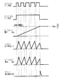
FIG. 2 shows the operation of each part at the time of charge control. As in the conventional apparatus, the
[0023]
When the
[0024]
At this time, energy corresponding to the current I is accumulated in the
[0025]
Since the
[0026]
In this way, by providing the
[0027]
In addition, since the
[0028]
In the discharge control, as in the conventional device, the
[0029]
Note that the feature of this embodiment is that if the number of piezo stacks is such as a 6-cylinder engine and the configuration is such that the piezo stack to be charged is selected, the
[0030]
(Second Embodiment)
FIG. 3 shows the configuration of a piezo actuator driving circuit according to the second embodiment of the present invention. This embodiment is configured to drive a single piezo actuator in the first embodiment, and only one piezo stack of the piezo actuator is connected. In the figure, parts that operate substantially the same as those in the first embodiment are denoted by the same reference numerals as those in the first embodiment, and differences from the first embodiment will be mainly described.
[0031]
In the piezo
[0032]
The
[0033]
In the above embodiment, the switching
[Brief description of the drawings]
FIG. 1 is a circuit diagram of a first piezo actuator drive circuit to which the present invention is applied.
FIG. 2 is a timing chart showing the operation of the piezo actuator drive circuit.
FIG. 3 is a circuit diagram of a second piezo actuator drive circuit to which the present invention is applied.
FIG. 4 is a schematic circuit diagram of a typical example of a conventional piezo actuator driving circuit.
FIG. 5 is a timing chart showing the operation of the piezo actuator drive circuit.
[Explanation of symbols]
1, 1A Piezo
12a, 12b, 12c
141
161A, 161B, 161C, 161D, 191
2A, 2B, 2C, 2D, 2 Piezo stack
Claims (3)
かつ、該コンデンサからインダクタを介してピエゾスタックに通電する第1の通電経路を有し、該通電経路には、前記コンデンサと前記通電経路の間に介設される充電用のスイッチング素子のオン期間に充電電流を流し、
前記コンデンサおよび前記スイッチング素子をバイパスしてインダクタからピエゾスタックに通電する第2の通電経路を有し、該通電経路には、前記スイッチング素子のオフ期間にフライホイール作用で前記ピエゾスタックへの充電可能な充電電流を流し、
かつ、前記スイッチング素子を制御しピエゾスタックが目標充電量に達するとスイッチング素子をオフに固定する制御手段を具備するピエゾアクチュエータ駆動回路において、
前記ピエゾスタックと前記第2の通電経路の間に介設されて、前記スイッチング素子がオフに固定されるのと同じタイミングで前記制御手段によりオフされてピエゾスタックを第2の通電経路から切断する通電経路切断用のスイッチング素子と、
インダクタからピエゾスタックに到る途中で第2の通電経路から分岐し、前記通電経路切断用のスイッチング素子がオフすると実質的にインダクタと前記コンデンサとを接続して前記フライホイール作用でインダクタから前記コンデンサに還流電流を流す第3の通電経路とを具備することを特徴とするピエゾアクチュエータ駆動回路。A capacitor for storing electric charge to be supplied to the piezo stack provided in the piezo actuator;
And a first energization path for energizing the piezo stack from the capacitor via the inductor, wherein the energization path includes an on period of a charging switching element interposed between the capacitor and the energization path. The charging current to
There is a second energization path that bypasses the capacitor and the switching element to energize the piezo stack from the inductor, and the energization path can charge the piezo stack by flywheel action during the off period of the switching element A large charging current,
And in the piezo actuator drive circuit comprising control means for controlling the switching element and fixing the switching element to OFF when the piezo stack reaches a target charge amount,
It is interposed between the piezo stack and the second energization path, and is turned off by the control means at the same timing as the switching element is fixed to be off, thereby disconnecting the piezo stack from the second energization path. A switching element for cutting the energization path;
Branching from the second energization path on the way from the inductor to the piezo stack, and when the switching element for disconnecting the energization path is turned off, the inductor and the capacitor are substantially connected to each other by the flywheel action. A piezo actuator drive circuit comprising: a third energization path through which a reflux current flows.
前記制御手段は、前記充電用のスイッチング素子がオフに固定されるのと一緒に前記ピエゾアクチュエータ選択用のスイッチング素子がオフするように設定し、
前記ピエゾアクチュエータ選択用のスイッチング素子を前記通電経路切断用のスイッチング素子と兼用としたピエゾアクチュエータ駆動回路。The piezoelectric actuator driving circuit according to claim 1 or 2, wherein a plurality of sets of the piezoelectric stack and a piezoelectric actuator selection switching element connected in series are connected in parallel to the output end of the inductor,
The control means is set so that the switching element for selecting the piezo actuator is turned off together with the switching element for charging being fixed off,
A piezoelectric actuator driving circuit in which the switching element for selecting the piezoelectric actuator is also used as the switching element for cutting the energization path.
Priority Applications (2)
| Application Number | Priority Date | Filing Date | Title |
|---|---|---|---|
| JP2000352183A JP4318849B2 (en) | 2000-11-20 | 2000-11-20 | Piezo actuator drive circuit |
| DE10151421A DE10151421A1 (en) | 2000-10-19 | 2001-10-18 | The piezo operating element drive circuit for fuel injection unit of motor vehicle, has piezo stack and control circuit which adjusts on period of switching system |
Applications Claiming Priority (1)
| Application Number | Priority Date | Filing Date | Title |
|---|---|---|---|
| JP2000352183A JP4318849B2 (en) | 2000-11-20 | 2000-11-20 | Piezo actuator drive circuit |
Publications (2)
| Publication Number | Publication Date |
|---|---|
| JP2002159190A JP2002159190A (en) | 2002-05-31 |
| JP4318849B2 true JP4318849B2 (en) | 2009-08-26 |
Family
ID=18825118
Family Applications (1)
| Application Number | Title | Priority Date | Filing Date |
|---|---|---|---|
| JP2000352183A Expired - Fee Related JP4318849B2 (en) | 2000-10-19 | 2000-11-20 | Piezo actuator drive circuit |
Country Status (1)
| Country | Link |
|---|---|
| JP (1) | JP4318849B2 (en) |
Families Citing this family (3)
| Publication number | Priority date | Publication date | Assignee | Title |
|---|---|---|---|---|
| KR100705004B1 (en) | 2005-07-11 | 2007-04-09 | 삼성전기주식회사 | Piezo Actuator Drive Circuit |
| JP4792899B2 (en) | 2005-09-29 | 2011-10-12 | ブラザー工業株式会社 | Optical scanning device and retinal scanning display device including the same |
| JP5029654B2 (en) * | 2009-05-27 | 2012-09-19 | 株式会社デンソー | Electronic control device |
-
2000
- 2000-11-20 JP JP2000352183A patent/JP4318849B2/en not_active Expired - Fee Related
Also Published As
| Publication number | Publication date |
|---|---|
| JP2002159190A (en) | 2002-05-31 |
Similar Documents
| Publication | Publication Date | Title |
|---|---|---|
| US6016040A (en) | Device and method for driving at least one capacitive actuator | |
| JP4383453B2 (en) | Driving circuit for an injector device | |
| WO1991017351A1 (en) | An apparatus for driving a piezoelectric actuator | |
| CN1156033C (en) | Device and method for controlling at least one capacitive actuator | |
| JP2007506038A5 (en) | ||
| US8149559B2 (en) | Piezoelectric actuator driving device and method | |
| JP2000501473A (en) | Apparatus and method for controlling at least one capacitive adjustment member | |
| KR100662145B1 (en) | Method and apparatus for driving one or more capacitive control elements | |
| US6661155B2 (en) | Method and device for controlling at least one capacitive actuator | |
| US7732976B2 (en) | Piezoelectric actuator drive device | |
| US6081062A (en) | Method and device for driving at least one capacitive actuator | |
| JP4104498B2 (en) | Piezo actuator drive circuit | |
| JP4318849B2 (en) | Piezo actuator drive circuit | |
| US20050231170A1 (en) | Circuit configuration for charging and discharging a plurality of capacitive actuators | |
| JP2010522839A (en) | Drive control circuit and drive control method for piezoelectric element | |
| CN101911454A (en) | Voltage pulse train generator, application to the control of an ultrasound piezoelectric injector | |
| JP3765286B2 (en) | Piezo actuator drive circuit | |
| JP2002246667A (en) | Piezo actuator driving circuit and fuel jetting device | |
| JP4622112B2 (en) | Piezo actuator driving circuit and fuel injection device | |
| JP4942663B2 (en) | Electric drive for ultrasonic piezoelectric actuator | |
| JPH0786657A (en) | Piezo-actuator driving device | |
| USRE38470E1 (en) | Method and device for driving at least one capacitive actuator | |
| KR100573847B1 (en) | Piezo Injector Drive of Diesel Common Rail System | |
| JP3067425B2 (en) | Piezo element drive circuit | |
| JP2002299707A (en) | Piezoelectric actuator dedriving circuit and fuel injection equipment |
Legal Events
| Date | Code | Title | Description |
|---|---|---|---|
| A621 | Written request for application examination |
Free format text: JAPANESE INTERMEDIATE CODE: A621 Effective date: 20061213 |
|
| A977 | Report on retrieval |
Free format text: JAPANESE INTERMEDIATE CODE: A971007 Effective date: 20090519 |
|
| TRDD | Decision of grant or rejection written | ||
| A01 | Written decision to grant a patent or to grant a registration (utility model) |
Free format text: JAPANESE INTERMEDIATE CODE: A01 Effective date: 20090526 |
|
| A01 | Written decision to grant a patent or to grant a registration (utility model) |
Free format text: JAPANESE INTERMEDIATE CODE: A01 |
|
| A61 | First payment of annual fees (during grant procedure) |
Free format text: JAPANESE INTERMEDIATE CODE: A61 Effective date: 20090527 |
|
| FPAY | Renewal fee payment (event date is renewal date of database) |
Free format text: PAYMENT UNTIL: 20120605 Year of fee payment: 3 |
|
| R150 | Certificate of patent or registration of utility model |
Free format text: JAPANESE INTERMEDIATE CODE: R150 |
|
| FPAY | Renewal fee payment (event date is renewal date of database) |
Free format text: PAYMENT UNTIL: 20120605 Year of fee payment: 3 |
|
| FPAY | Renewal fee payment (event date is renewal date of database) |
Free format text: PAYMENT UNTIL: 20130605 Year of fee payment: 4 |
|
| FPAY | Renewal fee payment (event date is renewal date of database) |
Free format text: PAYMENT UNTIL: 20140605 Year of fee payment: 5 |
|
| R250 | Receipt of annual fees |
Free format text: JAPANESE INTERMEDIATE CODE: R250 |
|
| LAPS | Cancellation because of no payment of annual fees |