JP4318768B2 - Method for manufacturing semiconductor device - Google Patents
Method for manufacturing semiconductor device Download PDFInfo
- Publication number
- JP4318768B2 JP4318768B2 JP15230898A JP15230898A JP4318768B2 JP 4318768 B2 JP4318768 B2 JP 4318768B2 JP 15230898 A JP15230898 A JP 15230898A JP 15230898 A JP15230898 A JP 15230898A JP 4318768 B2 JP4318768 B2 JP 4318768B2
- Authority
- JP
- Japan
- Prior art keywords
- film
- silicon film
- crystal
- semiconductor device
- amorphous silicon
- Prior art date
- Legal status (The legal status is an assumption and is not a legal conclusion. Google has not performed a legal analysis and makes no representation as to the accuracy of the status listed.)
- Expired - Fee Related
Links
Images


Classifications
-
- H10P14/3466—
-
- G—PHYSICS
- G02—OPTICS
- G02F—OPTICAL DEVICES OR ARRANGEMENTS FOR THE CONTROL OF LIGHT BY MODIFICATION OF THE OPTICAL PROPERTIES OF THE MEDIA OF THE ELEMENTS INVOLVED THEREIN; NON-LINEAR OPTICS; FREQUENCY-CHANGING OF LIGHT; OPTICAL LOGIC ELEMENTS; OPTICAL ANALOGUE/DIGITAL CONVERTERS
- G02F1/00—Devices or arrangements for the control of the intensity, colour, phase, polarisation or direction of light arriving from an independent light source, e.g. switching, gating or modulating; Non-linear optics
- G02F1/01—Devices or arrangements for the control of the intensity, colour, phase, polarisation or direction of light arriving from an independent light source, e.g. switching, gating or modulating; Non-linear optics for the control of the intensity, phase, polarisation or colour
- G02F1/13—Devices or arrangements for the control of the intensity, colour, phase, polarisation or direction of light arriving from an independent light source, e.g. switching, gating or modulating; Non-linear optics for the control of the intensity, phase, polarisation or colour based on liquid crystals, e.g. single liquid crystal display cells
- G02F1/133—Constructional arrangements; Operation of liquid crystal cells; Circuit arrangements
- G02F1/1333—Constructional arrangements; Manufacturing methods
- G02F1/1345—Conductors connecting electrodes to cell terminals
- G02F1/13454—Drivers integrated on the active matrix substrate
-
- H—ELECTRICITY
- H10—SEMICONDUCTOR DEVICES; ELECTRIC SOLID-STATE DEVICES NOT OTHERWISE PROVIDED FOR
- H10D—INORGANIC ELECTRIC SEMICONDUCTOR DEVICES
- H10D30/00—Field-effect transistors [FET]
- H10D30/01—Manufacture or treatment
- H10D30/021—Manufacture or treatment of FETs having insulated gates [IGFET]
- H10D30/031—Manufacture or treatment of FETs having insulated gates [IGFET] of thin-film transistors [TFT]
- H10D30/0312—Manufacture or treatment of FETs having insulated gates [IGFET] of thin-film transistors [TFT] characterised by the gate electrodes
- H10D30/0314—Manufacture or treatment of FETs having insulated gates [IGFET] of thin-film transistors [TFT] characterised by the gate electrodes of lateral top-gate TFTs comprising only a single gate
-
- H—ELECTRICITY
- H10—SEMICONDUCTOR DEVICES; ELECTRIC SOLID-STATE DEVICES NOT OTHERWISE PROVIDED FOR
- H10D—INORGANIC ELECTRIC SEMICONDUCTOR DEVICES
- H10D30/00—Field-effect transistors [FET]
- H10D30/01—Manufacture or treatment
- H10D30/021—Manufacture or treatment of FETs having insulated gates [IGFET]
- H10D30/031—Manufacture or treatment of FETs having insulated gates [IGFET] of thin-film transistors [TFT]
- H10D30/0321—Manufacture or treatment of FETs having insulated gates [IGFET] of thin-film transistors [TFT] comprising silicon, e.g. amorphous silicon or polysilicon
-
- H—ELECTRICITY
- H10—SEMICONDUCTOR DEVICES; ELECTRIC SOLID-STATE DEVICES NOT OTHERWISE PROVIDED FOR
- H10D—INORGANIC ELECTRIC SEMICONDUCTOR DEVICES
- H10D30/00—Field-effect transistors [FET]
- H10D30/60—Insulated-gate field-effect transistors [IGFET]
- H10D30/67—Thin-film transistors [TFT]
- H10D30/6729—Thin-film transistors [TFT] characterised by the electrodes
- H10D30/673—Thin-film transistors [TFT] characterised by the electrodes characterised by the shapes, relative sizes or dispositions of the gate electrodes
- H10D30/6731—Top-gate only TFTs
-
- H—ELECTRICITY
- H10—SEMICONDUCTOR DEVICES; ELECTRIC SOLID-STATE DEVICES NOT OTHERWISE PROVIDED FOR
- H10D—INORGANIC ELECTRIC SEMICONDUCTOR DEVICES
- H10D30/00—Field-effect transistors [FET]
- H10D30/60—Insulated-gate field-effect transistors [IGFET]
- H10D30/67—Thin-film transistors [TFT]
- H10D30/674—Thin-film transistors [TFT] characterised by the active materials
- H10D30/6741—Group IV materials, e.g. germanium or silicon carbide
- H10D30/6743—Silicon
- H10D30/6744—Monocrystalline silicon
-
- H—ELECTRICITY
- H10—SEMICONDUCTOR DEVICES; ELECTRIC SOLID-STATE DEVICES NOT OTHERWISE PROVIDED FOR
- H10D—INORGANIC ELECTRIC SEMICONDUCTOR DEVICES
- H10D30/00—Field-effect transistors [FET]
- H10D30/60—Insulated-gate field-effect transistors [IGFET]
- H10D30/67—Thin-film transistors [TFT]
- H10D30/674—Thin-film transistors [TFT] characterised by the active materials
- H10D30/6741—Group IV materials, e.g. germanium or silicon carbide
- H10D30/6743—Silicon
- H10D30/6745—Polycrystalline or microcrystalline silicon
-
- H—ELECTRICITY
- H10—SEMICONDUCTOR DEVICES; ELECTRIC SOLID-STATE DEVICES NOT OTHERWISE PROVIDED FOR
- H10D—INORGANIC ELECTRIC SEMICONDUCTOR DEVICES
- H10D62/00—Semiconductor bodies, or regions thereof, of devices having potential barriers
- H10D62/40—Crystalline structures
-
- H—ELECTRICITY
- H10—SEMICONDUCTOR DEVICES; ELECTRIC SOLID-STATE DEVICES NOT OTHERWISE PROVIDED FOR
- H10D—INORGANIC ELECTRIC SEMICONDUCTOR DEVICES
- H10D84/00—Integrated devices formed in or on semiconductor substrates that comprise only semiconducting layers, e.g. on Si wafers or on GaAs-on-Si wafers
- H10D84/01—Manufacture or treatment
- H10D84/02—Manufacture or treatment characterised by using material-based technologies
- H10D84/03—Manufacture or treatment characterised by using material-based technologies using Group IV technology, e.g. silicon technology or silicon-carbide [SiC] technology
- H10D84/038—Manufacture or treatment characterised by using material-based technologies using Group IV technology, e.g. silicon technology or silicon-carbide [SiC] technology using silicon technology, e.g. SiGe
-
- H—ELECTRICITY
- H10—SEMICONDUCTOR DEVICES; ELECTRIC SOLID-STATE DEVICES NOT OTHERWISE PROVIDED FOR
- H10D—INORGANIC ELECTRIC SEMICONDUCTOR DEVICES
- H10D86/00—Integrated devices formed in or on insulating or conducting substrates, e.g. formed in silicon-on-insulator [SOI] substrates or on stainless steel or glass substrates
- H10D86/01—Manufacture or treatment
- H10D86/021—Manufacture or treatment of multiple TFTs
- H10D86/0221—Manufacture or treatment of multiple TFTs comprising manufacture, treatment or patterning of TFT semiconductor bodies
- H10D86/0223—Manufacture or treatment of multiple TFTs comprising manufacture, treatment or patterning of TFT semiconductor bodies comprising crystallisation of amorphous, microcrystalline or polycrystalline semiconductor materials
- H10D86/0225—Manufacture or treatment of multiple TFTs comprising manufacture, treatment or patterning of TFT semiconductor bodies comprising crystallisation of amorphous, microcrystalline or polycrystalline semiconductor materials using crystallisation-promoting species, e.g. using a Ni catalyst
-
- H—ELECTRICITY
- H10—SEMICONDUCTOR DEVICES; ELECTRIC SOLID-STATE DEVICES NOT OTHERWISE PROVIDED FOR
- H10D—INORGANIC ELECTRIC SEMICONDUCTOR DEVICES
- H10D88/00—Three-dimensional [3D] integrated devices
-
- H—ELECTRICITY
- H10—SEMICONDUCTOR DEVICES; ELECTRIC SOLID-STATE DEVICES NOT OTHERWISE PROVIDED FOR
- H10D—INORGANIC ELECTRIC SEMICONDUCTOR DEVICES
- H10D88/00—Three-dimensional [3D] integrated devices
- H10D88/01—Manufacture or treatment
-
- H10P14/24—
-
- H10P14/3411—
-
- H10P14/3454—
-
- H10P14/3456—
-
- H10P14/38—
-
- H10P14/3802—
-
- H10P14/3806—
-
- H10P36/03—
-
- Y—GENERAL TAGGING OF NEW TECHNOLOGICAL DEVELOPMENTS; GENERAL TAGGING OF CROSS-SECTIONAL TECHNOLOGIES SPANNING OVER SEVERAL SECTIONS OF THE IPC; TECHNICAL SUBJECTS COVERED BY FORMER USPC CROSS-REFERENCE ART COLLECTIONS [XRACs] AND DIGESTS
- Y10—TECHNICAL SUBJECTS COVERED BY FORMER USPC
- Y10S—TECHNICAL SUBJECTS COVERED BY FORMER USPC CROSS-REFERENCE ART COLLECTIONS [XRACs] AND DIGESTS
- Y10S438/00—Semiconductor device manufacturing: process
- Y10S438/973—Substrate orientation
Landscapes
- Physics & Mathematics (AREA)
- Nonlinear Science (AREA)
- Mathematical Physics (AREA)
- Chemical & Material Sciences (AREA)
- Crystallography & Structural Chemistry (AREA)
- General Physics & Mathematics (AREA)
- Optics & Photonics (AREA)
- Thin Film Transistor (AREA)
- Recrystallisation Techniques (AREA)
Abstract
Description
【0001】
【発明が属する技術分野】
本明細書で開示する発明は、絶縁表面を有する基板上に形成された半導体薄膜およびそれを活性層とする半導体装置に関する。特に、半導体薄膜として珪素(シリコン)を主成分とする材料を利用する場合の構成に関する。
【0002】
また、薄膜トランジスタの如き半導体装置で構成された半導体回路および電気光学装置並びにそれらを搭載した電子機器の構成に関する。
【0003】
なお、本明細書中では上記薄膜トランジスタ、半導体回路、電気光学装置および電子機器を全て「半導体装置」に範疇に含めて扱う。即ち、半導体特性を利用して機能しうる装置全てを半導体装置と呼ぶ。従って、上記特許請求の範囲に記載された半導体装置は、薄膜トランジスタ等の単体素子だけでなく、それを集積化した半導体回路や電気光学装置およびそれらを部品として搭載した電子機器をも包含する。
【0004】
【従来の技術】
近年、絶縁表面を有する基板上に形成された半導体薄膜(厚さ数十〜数百nm程度)を用いて薄膜トランジスタ(TFT)を構成する技術が注目されている。薄膜トランジスタは特に画像表示装置(例えば液晶表示装置)のスイッチング素子としての開発が急がれている。
【0005】
例えば、液晶表示装置においてはマトリクス状に配列された画素領域を個々に制御する画素マトリクス回路、画素マトリクス回路を制御する駆動回路、さらに外部からのデータ信号を処理するロジック回路(演算回路、メモリ回路、クロックジェネレータなど)等のあらゆる電気回路にTFTを応用する試みがなされている。
【0006】
現状においては、活性層として非晶質珪素膜(アモルファスシリコン膜)を用いたTFTが実用化されているが、駆動回路やロジック回路などの様に、さらなる高速動作性能を求められる電気回路には、結晶性珪素膜(ポリシリコン膜等)を利用したTFTが必要とされる。
【0007】
例えば、ガラス基板上に結晶性珪素膜を形成する方法としては、本出願人による特開平7-130652号公報、特開平8-78329 号公報に記載された技術が公知である。これらの公報記載の技術は、非晶質珪素膜の結晶化を助長する触媒元素を利用することにより、500 〜600 ℃、4時間程度の加熱処理によって結晶性の優れた結晶性珪素膜を形成することを可能とするものである。
【0008】
特に、特開平8-78329 に記載された技術は上記技術を応用して基板面とほぼ平行な結晶成長を行わすものであり、発明者らは形成された結晶化領域を特に横成長領域(またはラテラル成長領域)と呼んでいる。
【0009】
しかし、この様なTFTを用いて駆動回路を構成してもまだまだ要求される性能を完全に満たすには及ばない。特に、メガヘルツからギガヘルツにかけての極めて高速な動作を要求する高速ロジック回路を従来のTFTで構成することは不可能なのが現状である。
【0010】
【発明が解決しようとする課題】
本発明者らは、これまで結晶粒界を有する結晶性珪素膜(ポリシリコン膜と呼ばれる)の結晶性を向上させるために様々な思考錯誤を繰り返してきた。セミアモルファス半導体(特開昭57-160121 号公報等)やモノドメイン半導体(特開平8-139019号公報等)などが挙げられる。
【0011】
上記公報に記載された半導体膜に共通の概念は、結晶粒界の実質的な無害化にある。即ち、結晶粒界を実質的になくし、キャリア(電子または正孔)の移動を円滑に行わせることが最大の課題であった。
【0012】
しかしながら、上記公報に記載された半導体膜をもってしてもロジック回路が要求する高速動作を行うには不十分と言える。即ち、ロジック回路を内蔵したシステム・オン・パネルを実現するためには、従来にない全く新しい材料の開発が求められているのである。
【0013】
本願発明は、その様な要求に答えるものであり、従来のTFTでは作製不可能であった様な高速ロジック回路を構成しうる極めて高性能な半導体装置を実現するための半導体薄膜を提供することを課題とする。また、その様な半導体薄膜を利用した半導体装置を提供することを課題とする。
【0014】
【課題を解決するための手段】
本明細書で開示する発明の構成は、
珪素を主成分とする複数の棒状または偏平棒状結晶の集合体からなる半導体薄膜であって、
主たる配向面は概略{110}面であり、
膜中に存在するC(炭素)及びN(窒素)の濃度が 5×10¹⁷atoms/cm3 以下、O(酸素)の濃度が 1×10¹⁸atoms/cm3 以下であり、
前記複数の棒状または偏平棒状結晶は互いに回転角をもって接しており、且つ、当該回転角の絶対値が3°以内であることを特徴とする。
【0015】
また、上記構成において、前記半導体薄膜の電子線回折パターンには{110}配向による特定の規則性が観測され、
当該電子線回折パターンの任意の回折スポットは概略円状であり、
前記回折スポットの短軸の長さ(a)と長軸の長さ(b)との比(a/b)が1/1(円形)〜1/1.5 であることを特徴とする。
【0016】
また、上記構成において、前記半導体薄膜の電子線回折パターンには{110}配向による特定の規則性が観測され、
当該電子線回折パターンの任意の回折スポットは、電子線照射エリアの中心点に対して同心円状の広がりを有し、
前記電子線照射エリアの中心点から前記回折スポットに対して引いた接線と、前記電子線照射エリアの中心点と前記回折スポットの中心点とを結ぶ線分と、がなす角は±1.5 °以内であることを特徴とする。
【0017】
以上に示す構成でなる本願発明について、以下に示す実施例をもって詳細な説明を行うこととする。
【0018】
【実施例】
〔実施例1〕
本実施例では、本願発明である半導体薄膜およびそれを活性層とした半導体装置(具体的にはTFT)の作製工程について説明する。
【0019】
まず、絶縁表面を有する基板としてシリコン基板501を準備する。シリコン基板501は水素熱処理を施して脱酸素化した基板を用いる。そして、シリコン基板501に対してハロゲン化物ガス(本実施例ではHCl)を含有する雰囲気での熱酸化処理を行い、熱酸化膜502を形成する。
【0020】
この様にして形成された熱酸化膜502は極めて平坦性に優れているという特徴を有する。本実施例では熱酸化条件を最適化することで、凹部と凸部との差の平均値が5nm以下(代表的には3nm以下、好ましくは2nm以下)、或いは100個の凹凸を調べれば、100個全ての凹凸の差が10nm以下で、且つ、その内の90個の凹凸の差が5nm以下である様な熱酸化膜を得られる。
【0021】
こうして図5(A)に示す様に極めて平坦な絶縁表面を有する基板が得られる。この優れた平坦性が本願発明の半導体薄膜を形成するにあたって重要な役割を果たす。
【0022】
次に、非晶質珪素膜503を形成する。非晶質珪素膜503は最終的な膜厚(熱酸化後の膜減りを考慮した膜厚)が10〜75nm(好ましくは15〜45nm)となる様に調節する。本実施例では成膜を減圧熱CVD法で行い、下記条件に従って形成する。

なお、成膜に際して膜中の不純物濃度の管理を徹底的に行うことが重要である。本実施例の場合、非晶質珪素膜503中では結晶化を阻害する不純物であるC(炭素)及びN(窒素)の濃度はいずれも 5×10¹⁸atoms/cm3 未満(代表的には 5×10¹⁷atoms/cm3 以下、好ましくは 2×10¹⁷atoms/cm3 以下)、O(酸素)は 1.5×10¹⁹atoms/cm3 未満(代表的には 1×10¹⁸atoms/cm3 以下、好ましくは 5×10¹⁷atoms/cm3 以下)となる様に管理する。なぜならば各不純物がこれ以上の濃度で存在すると、後の結晶化の際に悪影響を及ぼし、結晶化後の膜質を低下させる原因となるからである。
【0024】
ここで本実施例の条件で作製した非晶質珪素膜中の不純物濃度をSIMS(質量二次イオン分析)で調べた結果を図13に示す。なお、試料はシリコンウェハー上に0.5 μmの膜厚の非晶質珪素膜を成膜したものを用いた。その結果、図13に示す様にC、N、Oいずれの元素も上記濃度範囲内に収まることが確認された。ただし、本明細書中において膜中の元素濃度は、SIMSの測定結果における最小値で定義される。
【0025】
上記構成を得るため、本実施例で用いる減圧熱CVD炉は定期的にドライクリーニングを行い、成膜室の清浄化を図っておくことが望ましい。ドライクリーニングは、 200〜400 ℃程度に加熱した炉内に 100〜300sccm のClF3 (フッ化塩素)ガスを流し、熱分解によって生成したフッ素によって成膜室のクリーニングを行えば良い。
【0026】
なお、本発明者らの知見によれば炉内温度300 ℃とし、ClF3 (フッ化塩素)ガスの流量を300sccm とした場合、約2μm厚の付着物(主に珪素を主成分する)を4時間で完全に除去することができる。
【0027】
また、非晶質珪素膜503中の水素濃度も非常に重要なパラメータであり、水素含有量を低く抑えた方が結晶性の良い膜が得られる様である。そのため、非晶質珪素膜503の成膜は減圧熱CVD法であることが好ましい。なお、成膜条件を最適化することでプラズマCVD法を用いることも可能である。
【0028】
次に、非晶質珪素膜503の結晶化工程を行う。結晶化の手段としては本発明者による特開平7-130652号公報記載の技術を用いる。同公報の実施例1および実施例2のどちらの手段でも良いが、本願発明では実施例2に記載した技術内容(特開平8-78329 号公報に詳しい)を利用するのが好ましい。
【0029】
特開平8-78329 号公報記載の技術は、まず触媒元素の添加領域を選択するマスク絶縁膜504を形成する。そして、非晶質珪素膜503の結晶化を助長する触媒元素としてニッケル(Ni)を含有した溶液をスピンコート法により塗布し、Ni含有層505を形成する。(図5(B))
【0030】
なお、触媒元素としてはニッケル以外にも、コバルト(Co)、鉄(Fe)、パラジウム(Pd)、白金(Pt)、銅(Cu)、金(Au)、ゲルマニウム(Ge)、鉛(Pb)、インジウム(In)等を用いることができる。
【0031】
また、上記触媒元素の添加工程はスピンコート法に限らず、レジストマスクを利用したイオン注入法またはプラズマドーピング法を用いることもできる。この場合、添加領域の占有面積の低減、横成長領域の成長距離の制御が容易となるので、微細化した回路を構成する際に有効な技術となる。
【0032】
次に、触媒元素の添加工程が終了したら、450 ℃1時間程度の水素出しの後、不活性雰囲気、水素雰囲気または酸素雰囲気中において 500〜700 ℃(代表的には 550〜650 ℃)の温度で 4〜24時間の加熱処理を加えて非晶質珪素膜503の結晶化を行う。本実施例では窒素雰囲気で570 ℃14時間の加熱処理を行う。
【0033】
この時、非晶質珪素膜503の結晶化はニッケルを添加した領域506で発生した核から優先的に進行し、基板501の基板面に対してほぼ平行に成長した結晶領域507が形成される。本発明者らはこの結晶領域507を横成長領域と呼んでいる。横成長領域は比較的揃った状態で個々の結晶が集合しているため、全体的な結晶性に優れるという利点がある。(図5(C))
【0034】
結晶化のための加熱処理が終了したら、マスク絶縁膜504を除去してパターニングを行い、横成長領域507のみでなる島状半導体層(活性層)508を形成する。次に、珪素を含む絶縁膜でなるゲイト絶縁膜509を形成する。ゲイト絶縁膜509の膜厚は後の熱酸化工程による増加分も考慮して20〜250nm の範囲で調節すれば良い。また、成膜方法は公知の気相法(プラズマCVD法、スパッタ法等)を用いれば良い。
【0035】
次に、図5(D)に示す様に触媒元素(ニッケル)を除去または低減するための加熱処理(触媒元素のゲッタリングプロセス)を行う。この加熱処理は処理雰囲気中にハロゲン元素を含ませ、ハロゲン元素による金属元素のゲッタリング効果を利用するものである。
【0036】
なお、ハロゲン元素によるゲッタリング効果を十分に得るためには、上記加熱処理を700 ℃を超える温度で行なうことが好ましい。この温度以下では処理雰囲気中のハロゲン化合物の分解が困難となり、ゲッタリング効果が得られなくなる恐れがある。そのため加熱処理温度を好ましくは800 〜1000℃(代表的には950 ℃)とし、処理時間は 0.1〜 6hr、代表的には 0.5〜 1hrとする。
【0037】
代表的な実施例としては酸素雰囲気中に対して塩化水素(HCl)を0.5 〜10体積%(本実施例では3体積%)の濃度で含有させた雰囲気中において、950 ℃、30分の加熱処理を行えば良い。HCl濃度を上記濃度以上とすると、活性層508の表面に膜厚程度の凹凸が生じてしまうため好ましくない。
【0038】
また、ハロゲン元素を含む化合物してはHClガス以外にもHF、NF3 、HBr、Cl2 、ClF3 、BCl3 、F2 、Br2 等のハロゲン元素を含む化合物から選ばれた一種または複数種のものを用いることが出来る。
【0039】
この工程においては活性層508中のニッケルが塩素の作用によりゲッタリングされ、揮発性の塩化ニッケルとなって大気中へ離脱して除去される。そして、この工程により活性層508中のニッケルの濃度は 5×10¹⁷atoms/cm3 以下(代表的には 2×10¹⁷atoms/cm3 以下)にまで低減される。なお、本発明者らの経験によれば、ニッケル濃度が 1×10¹⁸atoms/cm3 以下(好ましくは 5×10¹⁷atoms/cm3 以下)であればTFT特性に悪影響はでない。
【0040】
また、上記ゲッタリング処理はニッケル以外の他の金属元素にも効果的である。珪素膜中に混入しうる金属元素としては、主に成膜チャンバーの構成元素(代表的にはアルミニウム、鉄、クロム等)が考えられるが、上記ゲッタリング処理を行なえば、それら金属元素の濃度も 5×10¹⁷atoms/cm3 以下(好ましくは 2×10¹⁷atoms/cm3 以下)にすることが可能である。
【0041】
なお、上記ゲッタリング処理を行うと、活性層508中にはゲッタリング処理に使用したハロゲン元素が 1×10¹⁵〜 1×10²⁰atoms/cm3 の濃度で残存する。
【0042】
また、上記加熱処理により活性層508とゲイト絶縁膜509の界面では熱酸化反応が進行し、熱酸化膜の分だけゲイト絶縁膜509の膜厚は増加する。この様にして熱酸化膜を形成すると、非常に界面準位の少ない半導体/絶縁膜界面を得ることができる。また、活性層端部における熱酸化膜の形成不良(エッジシニング)を防ぐ効果もある。
【0043】
さらに、上記ハロゲン雰囲気における加熱処理を施した後に、窒素雰囲気中で950 ℃ 1時間程度の加熱処理を行なうことで、ゲイト絶縁膜509の膜質の向上を図ることも有効である。
【0044】
なお、このハロゲン元素によるゲッタリング工程は、結晶化工程とゲイト絶縁膜の成膜工程との間に行うこともできる。
【0045】
次に、図示しないアルミニウムを主成分とする金属膜を成膜し、パターニングによって後のゲイト電極の原型510を形成する。本実施例では2wt% のスカンジウムを含有したアルミニウム膜を用いる。なお、これ以外にもタンタル膜、導電性を有する珪素膜等を用いることもできる。(図5(E))
【0046】
ここで本発明者らによる特開平7-135318号公報記載の技術を利用する。同公報には、陽極酸化により形成した酸化膜を利用して自己整合的にソース/ドレイン領域と低濃度不純物領域とを形成する技術が開示されている。以下にその技術について簡単に説明する。
【0047】
まず、アルミニウム膜のパターニングに使用したレジストマスク(図示せず)を残したまま3%シュウ酸水溶液中で陽極酸化処理を行い、多孔性の陽極酸化膜511を形成する。この膜厚が後に低濃度不純物領域の長さになるのでそれに合わせて膜厚を制御する。
【0048】
次に、図示しないレジストマスクを除去した後、エチレングリコール溶液に3%の酒石酸を混合した電解溶液中で陽極酸化処理を行う。この処理では緻密な無孔性の陽極酸化膜512が形成される。膜厚は70〜120 nmで良い。
【0049】
そして、上述の2回に渡る陽極酸化処理の後に残ったアルミニウム膜513が実質的にゲイト電極として機能する。(図6(A))
【0050】
次にゲイト電極513、多孔性の陽極酸化膜511をマスクとしてゲイト絶縁膜509をドライエッチング法によりエッチングする。そして、多孔性の陽極酸化膜511を除去する。こうして形成されるゲイト絶縁膜514の端部は多孔性の陽極酸化膜511の膜厚分だけ露出した状態となる。(図6(B))
【0051】
次に、一導電性を付与する不純物元素の添加工程を行う。不純物元素としてはN型ならばP(リン)またはAs(砒素)、P型ならばB(ボロン)またはIn(インジウム)を用いれば良い。
【0052】
この工程では、まず1回目の不純物添加を高加速電圧で行い、n- 領域を形成する。この時、加速電圧が80keV 程度と高いので不純物元素は露出した活性層表面だけでなく露出したゲイト絶縁膜の端部の下にも添加される。さらに、2回目の不純物添加を低加速電圧で行い、n+ 領域を形成する。この時は加速電圧が10keV 程度と低いのでゲイト絶縁膜はマスクとして機能する。
【0053】
以上の工程で形成された不純物領域は、n+ 領域がソース領域515、ドレイン領域516となり、n- 領域が一対の低濃度不純物領域(LDD領域とも呼ばれる)517となる。また、ゲイト電極直下の領域は不純物元素が添加されず、真性または実質的に真性なチャネル形成領域518となる。(図6(C))
【0054】
以上の様にして活性層が完成したら、ファーネスアニール、レーザーアニール、ランプアニール等の組み合わせによって不純物元素の活性化を行う。それと同時に添加工程で受けた活性層の損傷も修復される。
【0055】
次に、層間絶縁膜519を500 nmの厚さに形成する。層間絶縁膜519としては酸化珪素膜、窒化珪素膜、酸化窒化珪素膜、有機性樹脂膜、或いはそれらの積層膜を用いることができる。
【0056】
次に、コンタクトホールを形成した後、ソース電極520、ドレイン電極521を形成する。最後に、基板全体を350 ℃の水素雰囲気で1〜2時間加熱し、素子全体の水素化を行うことで膜中(特に活性層中)のダングリングボンド(不対結合手)を終端する。以上の工程によって、図6(D)に示す様な構造のTFTを作製することができる。
【0057】
なお、本願発明は活性層を構成する半導体薄膜に関する技術であるので、その他の構造および構成は何ら本願発明を限定するものではない。従って、本願発明は本実施例以外の構造および構成を有するTFTに対しても容易に適用することが可能である。
【0058】
(活性層中に含まれる不純物に関する知見)
本実施例の活性層(半導体薄膜)には結晶化を阻害する元素であるC(炭素)、N(窒素)及びO(酸素)が存在しない、或いは実質的に存在しない点に特徴がある。これは徹底的な不純物(汚染物)管理によってなしうる構成である。
【0059】
本実施例の場合、非晶質珪素膜の成膜にあたってC(炭素)、N(窒素)及びO(酸素)の混入を徹底的に避けるので、必然的に最終的な半導体膜中に存在するC(炭素)及びN(窒素)の濃度は少なくとも 5×10¹⁸atoms/cm3 未満(代表的には 5×10¹⁷atoms/cm3 以下、好ましくは 2×10¹⁷atoms/cm3 以下)、O(酸素)の濃度は少なくとも 1.5×10¹⁹atoms/cm3 未満(代表的には 1×10¹⁸atoms/cm3 以下、好ましくは 5×10¹⁷atoms/cm3 以下)となる。
【0060】
なお、純粋に珪素だけからなる半導体膜では珪素の濃度が約 5×10²²atoms/cm3 であるので、例えば 5×10¹⁸atoms/cm3 の不純物元素は約0.01atomic% の濃度で存在することに相当する。
【0061】
また、望ましくは最終的な半導体膜中に存在するC(炭素)、N(窒素)及びO(酸素)の濃度をSIMS分析における検出下限以下、さらに望ましくは完全に存在しない状態とすることが優れた結晶性を得るためには必要である。
【0062】
本発明者らがSIMSで分析した結果、C、N、Oの濃度がいずれも上記濃度範囲を満たす非晶質珪素膜を出発膜として用いた場合、完成したTFTの活性層中に含まれるC、N、Oの濃度も上記濃度範囲を満たすことが判明している。
【0063】
〔活性層の結晶構造に関する知見〕
上記作製工程に従って形成した活性層は、微視的に見れば複数の棒状(または偏平棒状)結晶が互いに概略平行に特定方向への規則性をもって並んだ結晶構造を有する。このことはTEM(透過型電子顕微鏡法)による観察で容易に確認することができる。
【0064】
ここで、棒状または偏平棒状結晶同士の結晶粒界を 800万倍に拡大したHR−TEM写真を図17に示す。なお、本明細書中において結晶粒界とは、棒状または偏平棒状結晶が接した境界に形成される粒界を指すものと定義する。従って、例えば横成長領域がぶつかりあって形成される様なマクロな意味あいでの粒界とは区別して考える。
【0065】
ところで前述のHR−TEM(高分解能透過型電子顕微鏡法)とは、試料に対して垂直に電子線を照射し、透過電子や弾性散乱電子の干渉を利用して原子・分子配列を評価する手法である。
【0066】
HR−TEMでは結晶格子の配列状態を格子縞として観察することが可能である。従って、結晶粒界を観察することで、結晶粒界における原子同士の結合状態を推測することができる。なお、格子縞は白と黒の縞模様となって現れるが、コントラストの相違であって原子の位置を示すものではない。
【0067】
図17(A)は本願発明で得られる結晶性珪素膜の代表的なTEM写真であり、異なる二つの結晶粒が写真左上から右下にかけて見られる結晶粒界で接した状態が観察されている。この時、二つの結晶粒は結晶軸に多少のずれが含まれているものの概略{110}配向であった。
【0068】
なお、後述するが複数の結晶粒を調べた結果、殆ど全てが概略{110}配向であることをX線回折や電子線回折によって確認している。なお、多数観察した中には(011)面や(200)面などもあるはずだが、それら等価な面はまとめて{110}面と表すことにする。
【0069】
ところで、図17(A)に図示した様に、面内には{111}面、{100}面に対応する格子縞が観察されている。なお、{111}面に対応する格子縞とは、その格子縞に沿って結晶粒を切断した場合に断面に{111}面が現れる様な格子縞を指している。格子縞がどの様な面に対応するかは、簡易的に格子縞と格子縞の間隔から確認できる。
【0070】
なお、図17(A)において格子縞の見え方に差が見られるのは、結晶粒の微妙な傾きの違いによるものである。即ち、片方の結晶粒の結晶面に垂直に電子線が照射される様に設定すると、他方の結晶粒は僅かに斜めから電子線が照射される状態になるため、格子縞の見え方が変わるのである。
【0071】
ここで{111}面に対応する格子縞に注目する。図17(A)において粒界を挟んで上側の結晶粒の{111}面に対応する格子縞は、下側の結晶粒の{111}面に対応する格子縞と約70°(正確には70.5°)の角度をなして交わっている。
【0072】
この様な結晶構造(正確には結晶粒界の構造)は、結晶粒界において異なる二つの結晶粒が極めて整合性よく接合していることを示している。即ち、結晶粒界において結晶格子が連続的に連なり、結晶欠陥等に起因するトラップ準位を非常に作りにくい構成となっている。換言すれば、結晶粒界において結晶格子に連続性があるとも言える。
【0073】
なお、参考までに従来の高温ポリシリコン膜のHRーTEM写真を図17(B)に示す。図17(B)の場合、後述するが結晶面に規則性がなく、{110}面が主体となる配向ではなかった。ただし、ここでは図17(A)と比較するために{111}面に対応する格子縞が現れる様な結晶粒を観察した。
【0074】
図17(B)を詳細に観察して見ると、図中において矢印で示す様に、結晶粒界では格子縞が途切れた部分が多数確認できる。この様な部分では未結合手(結晶欠陥と呼べる)が存在することになる、トラップ準位としてキャリアの移動を阻害する可能性が高い。
【0075】
ただし、確かに本願発明の結晶性珪素膜にも図17(B)に示した様な未結合手は存在する。これは本願発明の結晶性珪素膜が多結晶である以上しかたのないことである。しかしながら、本願発明の結晶性珪素膜を広範囲に渡って詳細にTEM観察した結果、その様な未結合手はごく僅かであることが判明している。
【0076】
本出願人が調べた限りでは、全体の90%以上(典型的には95%以上)の結晶粒界に結晶格子の連続性が見られ、図17(B)に示した様な未結合手は殆ど見つけることができなかった。この事からも本願発明の結晶性珪素膜は従来の高温ポリシコンとは明らかに異なる半導体膜であると言えよう。
【0077】
次に、本願発明の半導体薄膜を電子線回折によって調べた結果を図1(A)に示す。また、リファレンスとして従来の高温ポリシリコン膜の電子線回折パターンを図1(B)に示す。なお、図1(A)、(B)において電子線の照射エリアの径はそれぞれ4.25μm、1.35μmである。本実施例では複数箇所を測定したうちの代表的な写真を示す。
【0078】
図1(A)の場合、〈110〉入射に対応する回折スポット(回折斑点)が比較的きれいに現れており、電子線の照射エリア内では殆ど全ての結晶粒が{110}配向していることが確認できる。
【0079】
なお、本出願人は特開平7−321339号公報に記載した手法に従ってX線回折を行い、本願発明の半導体薄膜について配向比率を算出した。同公報では下記数1に示す様な算出方法で配向比率を定義している。
【0080】
【数1】
本願発明の半導体薄膜の配向性をX線回折で調べた結果、X線回折パターンには(220)面に相当するピークが現れた。勿論、(220)は{110}と等価であることは言うまでもない。この測定の結果、{110}面が主たる配向面であり、配向比率は0.7 以上(典型的には0.9 以上)であることが判明した。
【0082】
一方、図1(B)に示す従来の高温ポリシリコン膜の場合、回折スポットには明瞭な規則性が見られず、ほぼランダムに配向している、換言すれば{110}面以外の面方位の結晶粒が不規則に混在することが判明した。
【0083】
なお、各回折スポットは同心円上の広がりを僅かにもっているが、これは結晶軸を中心にある程度の回転角の分布をもつためと予想される。この事について以下に説明する。
【0084】
図1(A)に示した電子線回折パターンの一部を模式的に図2(A)に示す。図2(A)において、201で示される複数の揮点は〈110〉入射に対応する回折スポットである。複数の回折スポット201は照射エリアの中心点202を中心にして同心円状に分布している。
【0085】
ここで、点線で囲まれた領域203を拡大したものを図2(B)に示す。図2(B)に示す様に、図1(A)に示す電子線回折パターンを詳細に観察すると、照射エリアの中心点202に対して回折スポット201が約±1.5 °の広がり(ゆらぎ)を持っていることが判る。
【0086】
即ち、電子線照射エリアの中心点202から回折スポット201に対して引いた接線204と、電子線照射エリアの中心点202と回折スポットの中心点205とを結ぶ線分と、がなす角(回転角の1/2に相当する)は1.5 °以下となることを意味している。この時、接線は2本引けるので、回折スポット201の広がりは結局±1.5 °以内の範囲に収まることになる。
【0087】
この傾向は図1(A)に示した電子線回折パターンの全域で見受けられ、全体としては±2.5 °以内(典型的には±1.5 °以内、好ましくは±0.5 °以内)に収まっている。前述の「各回折スポットは同心円上の広がりを僅かにもっている」という言葉はこの事を指している。
【0088】
また、半導体薄膜の下地を限りなく平坦にすることで、回折スポット201の短軸の長さ(a)と長軸の長さ(b)との比(a/b)を1/1(円形を意味する)〜1/1.5 としうる。これは、回折スポットが円形または実質的に円形になることを意味している。
【0089】
回折スポットが円形になるためには複数の結晶粒間に存在する回転角を非常に小さくしなければならない。単結晶の電子線回折パターンでは回折スポットが完全に円形になることを考えれば、回折スポットが円形になるという事は本願発明の半導体薄膜が限りなく単結晶に近づくことに他ならない。
【0090】
また、図3(A)は面方位が{110}である場合の結晶軸と、結晶面内に含まれる軸の関係を表している。この様に、結晶面が{110}配向であれば結晶軸は〈110〉軸であり、その結晶面内には〈111〉軸、〈100〉軸などが含まれる。
【0091】
また、以前に本発明者らがHR−TEMを利用して上記棒状結晶の成長方向を調べた結果、概略〈111〉軸方向に向かって成長することが確かめられている(特開平7-321339号公報参照)。従って、本願発明の半導体薄膜の一部を拡大すると図3(B)の様になっていると考えられる。
【0092】
図3(B)において、301〜303はそれぞれ異なる棒状結晶であり、個々の結晶粒の結晶軸は概略〈110〉軸である。また、結晶成長は平均的には概略〈111〉軸方向に向かって進行するので、棒状結晶の延在する方向と〈111〉軸方向とはほぼ一致する。なお、点線で示されるのは結晶粒界である。
【0093】
この時、任意の結晶粒301の面内に含まれる〈111〉軸304を基準軸とすると、近傍に存在する他の棒状結晶302、303の面内に含まれる〈111〉軸305、306は、基準軸304に一致するか、若しくはそれぞれ僅かづつずれて基準軸304に対してある程度の角度を持つ様になる。本明細書中ではこの角度を回転角と呼んでいる。
【0094】
なお、前述の回折スポットの広がりが±2.5 °以内(典型的には±1.5 °以内、好ましくは±0.5 °以内)に収まっているという事は、換言すれば回転角の絶対値が5°以内(典型的には3°以内、好ましくは1°以内)に収まっているという事と同義である。
【0095】
この関係を判りやすく図3(C)にまとめると、本願発明の半導体薄膜では軸305が基準軸304となす角(α)および軸306が基準軸304となす角(β)が回転角である。そして、この回転角が少なくとも5°以内に収まっているのである。
【0096】
そして、図3(B)の様に微妙な回転角を有する個々の結晶粒はそれぞれ異なる回折スポットとして電子線回折パターン上に現れる。例えば、結晶粒302、303の回折スポットは、結晶粒301の回折スポットから回転角α、β分だけ同心円上にずれて現れる。
【0097】
即ち、電子線の照射エリア内に複数の結晶粒が存在すれば、同心円上に複数の結晶粒に対応する回折スポットが連続的に並ぶことになり、回折スポットは見かけ上、楕円に近い形状を示す様になる。これが図1(A)の電子線回折パターンに回折スポットの広がりが見られた理由である。
【0098】
なお、本実施例では〈111〉等の様に表記しているが、その中には[111]や[1−11]など等価な複数の軸が含まれる(マイナス記号は反転を意味する)。即ち、等価な軸全てに対応して回折スポットが現れ、その結果として図1(A)の様な電子線回折パターンを形成しているので、結晶粒が回転角分だけ回転すれば電子線回折パターンも全体的に回転角分だけ回転する。そのため、全ての回折スポットが同心円上に広がりを持つ。
【0099】
以上の様に、本願発明の半導体薄膜を電子線回折で調べた結果として図1(A)の様な回折パターンが得られたのは、電子線の照射エリア内に複数の棒状結晶が存在し、それぞれが僅かに異なる回転角を有するためと解釈できる。また、その回折スポットの広がり具合から、回転角の絶対値は5°以内(典型的には3°以内、好ましくは1°以内)と考えられる。
【0100】
これは、本願発明の半導体薄膜を構成する全結晶粒のうち、最も大きな回転角を有する二つの結晶粒間においても、任意の基準軸のずれが少なくとも5°以内に収まっていることを意味している。
【0101】
ここで、一般的に行われている結晶粒界の分類に乗っ取り、本願発明の半導体薄膜における各種結晶粒界の存在度について説明する。次に示す表は、本願発明の半導体薄膜に関するデータを考慮したものである。
【0102】
【表1】
なお、表1に示した形態の結晶粒界は電子線回折、HR−TEM、断面TEM等を駆使することで識別が可能であり、さらにはより詳細な情報を得ることができる。なお、本明細書で取り扱う回転角の値は、上記手法を組み合わせて様々な角度から結晶粒界を解析することで測定している。
【0104】
前述の結晶軸まわりの回転は「粒界面に含まれる方位についての回転」であるので小傾角粒界に含まれる。この様なを結晶粒界を形成する場合、模式的には図4(A)に示す様な関係で二つの結晶粒は接している。この場合、二つの結晶粒の接する面が粒界面である。しかしながら、本願発明の半導体薄膜では結晶軸まわりの回転角が±2.5 °以内と極めて小さいので図4(A)の様な粒界は殆ど存在しないと見なすことができる。。
【0105】
また、小傾角粒界には図4(B)に示す様な場合もある。図4(B)の形態の場合、回転軸となる軸が図4(A)とは異なっている。しかし、粒界面に含まれる軸を中心にして二つの結晶粒がある回転角を有する関係にある点は図4(A)と同様である。本願発明の半導体薄膜では、この場合の回転角も±2.5 °以内(典型的には±1.5 °以内、好ましくは0.5 °以内)であるので、この様な結晶粒界も殆ど存在しないと見なすことができる。
【0106】
また、図4(A)、(B)に示した小傾角粒界とは区別されるが、同じ低角粒界の分類にねじれ粒界と呼ばれる形態がある。これは図4(C)に示す様に、粒界面に垂直な方位について回転した場合に相当する。
【0107】
この場合も、二つの結晶粒がある回転角を有する関係にある点は小傾角粒界と同様であり、本願発明の半導体薄膜では回転角が±2.5 °以内(典型的には±1.5 °以内、好ましくは0.5 °以内)に収まっている。即ち、ねじれ粒界も殆ど存在しないと見なすことができる。
【0108】
以上の様に、本願発明の半導体薄膜には一般的に低角粒界と呼ばれる電気的に活性な結晶粒界がない又は実質的にないと考えられる。なお、「電気的に活性」とはキャリアにとってトラップとして機能しうることを意味している。
【0109】
また、「実質的にない」とは、例えば5μm平方の範囲に含まれる結晶粒界を調べた時に、該当する粒界(例えば低角粒界等)が、観察されても1つや2つである様な場合を指す。
【0110】
また、特殊な高角粒界では双晶粒界とその他の対応粒界とがあるが、本願発明の半導体薄膜の殆どがこの双晶粒界であることが確認されている。この対応粒界は例え存在しても電気的に不活性(キャリアのトラップとして機能しない)であることが判っている。
【0111】
特に、本願発明の半導体薄膜はΣ3の対応粒界({111}双晶粒界)が全体の90%以上(典型的には95%以上)を占めており、極めて整合性の良い結晶粒界が形成されていることが広い範囲において証明されている。
【0112】
なお、Σ値は対応粒界の整合性の程度を示す指針となるパラメータであり、Σ値が小さいほど整合性の良い結晶粒界であることが知られている。Σ値の定義については「材料評価のための高分解能電子顕微鏡法;進藤大輔,平賀賢二共著,pp.54 〜60,共立出版株式会社,1996」に詳しい。
【0113】
二つの結晶粒の間に形成された結晶粒界において、両方の結晶の面方位が{110}である場合、{111}面に対応する格子縞がなす角をθとすると、θ=70.5°の時にΣ3の対応粒界となることが知られている。
【0114】
従って、図1(A)のTEM写真に示された結晶粒界では、隣接する結晶粒の各格子縞が70.5°の角度で連続しており、この結晶粒界は{111}双晶粒界であると容易に推察することができる。
【0115】
なお、θ= 38.9 °の時にはΣ9の対応粒界となるが、この様な他の対応粒界も若干ながら存在した。
【0116】
この様な対応粒界は、同一面方位の結晶粒間にしか形成されない。即ち、本願発明の半導体薄膜は面方位が概略{110}で揃っているからこそ、広範囲に渡ってこの様な対応粒界を形成しうるのである。この特徴は、面方位が不規則な他のポリシリコン膜ではあり得ることではない。
【0117】
また、ランダムな高角粒界とは有意な方位関係を持たずに不規則な方位の結晶粒が並んだだけの半導体薄膜に見られる粒界であり、従来の高温ポリシリコンなどの様な半導体薄膜に多く見られる。本願発明の半導体薄膜では、当然、高角粒界は殆ど存在しない。
【0118】
表1に示した低角粒界、ランダムな高角粒界の双方がない又は極めてその数が少ない場合、活性な結晶粒界は存在しないと見なせる。即ち、その様な結晶構造を有する半導体薄膜は実質的に結晶粒界のない単結晶又は実質的な単結晶と見なすことができる。
【0119】
以上の様に、本願発明の半導体薄膜は、薄膜を構成する個々の結晶粒(棒状結晶)が互いに完全に一致する方位関係にあるか、ある程度の回転角を有した関係にある。そして、その回転角は±2.5 °以内という非常に小さなものであり、実質的に活性な結晶粒界を形成しないと見なして良いレベルである。
【0120】
本発明者らは、この様な半導体薄膜が得られた理由として、下地の平坦性を重要視している。本発明者らの経験では、下地に凹凸があるとそれが結晶成長の際に大きく影響する。即ち、下地の凹凸等によって結晶粒にひずみ等が発生し、結晶軸のずれなどを引き起こすことになる。
【0121】
本願発明の半導体薄膜は、本実施例に示した様な方法で形成された非常に平坦性の高い下地膜上に形成されている。従って、結晶成長を阻害する要因を極力排除した状態で成長させることができるため、非常に高い結晶性を維持したまま結晶粒同士が接合する。その結果として、前述の様に実質的に単結晶と見なせる結晶性を有する半導体薄膜が得られたものと考えられる。
【0122】
なお、本発明の半導体薄膜を形成するにあたって結晶化温度以上の温度でのアニール工程(本実施例の場合、図5(D)に示す工程)は、結晶粒内の欠陥低減に関して重要な役割を果たしている。その事について説明する。
【0123】
図14(A)は図5(C)に示した結晶化工程までを終了した時点での結晶シリコン膜を25万倍に拡大したTEM写真であり、結晶粒内(黒い部分と白い部分はコントラストの差に起因して現れる)に矢印で示される様なジグザグ状に見える欠陥が確認される。
【0124】
この様な欠陥は主としてシリコン結晶格子面の原子の積み重ね順序が食い違っている積層欠陥であるが、転位などの場合もある。図14(A)は{111}面に平行な欠陥面を有する積層欠陥と思われる。その事は、ジグザグ状に見える欠陥が約70°の角をなして折れ曲がっていることから推測できる。
【0125】
一方、図14(B)に示す様に、同倍率で見た本発明の結晶シリコン膜は、結晶粒内には殆ど積層欠陥や転位などに起因する欠陥が見られず、非常に結晶性が高いことが確認できる。この傾向は膜面全体について言えることであり、欠陥数をゼロにすることは現状では困難であるが、実質的にゼロと見なせる程度にまで低減することができる。
【0126】
即ち、図14(B)に示す結晶シリコン膜は結晶粒内の欠陥が殆ど無視しうる程度にまで低減され、且つ、結晶粒界が高い連続性によってキャリア移動の障壁になりえないため、単結晶または実質的に単結晶と見なせる。
【0127】
この様に、図14(A)と(B)の写真に示した結晶シリコン膜は結晶粒界はほぼ同等の連続性を有しているが、結晶粒内の欠陥数には大きな差がある。本発明の結晶シリコン膜が図14(A)に示した結晶シリコン膜よりも遙に高い電気特性を示す理由はこの欠陥数の差によるところが大きい。
【0128】
本出願人は、図5(D)の工程によって起こる現象について次の様なモデルを考えている。まず、図14(A)に示す状態では結晶粒内の欠陥(主として積層欠陥)には触媒元素(代表的にはニッケル)が偏析している。即ち、Si-Ni-Siといった形の結合が多数存在していると考えられる。
【0129】
しかしながら、触媒元素のゲッタリングプロセスを行うことで欠陥に存在するNiが除去されると、Si-Ni 結合は切れる。そのため、シリコンの余った結合手はすぐにSi-Si 結合を形成して安定する。こうして欠陥が消滅する。
【0130】
勿論、高い温度での熱アニールによって結晶シリコン膜中の欠陥が消滅することは知られているが、本発明ではニッケルとの結合が切れて未結合手が多く発生するためシリコンの再結合がさらにスムーズに行われると推測できる。
【0131】
また、同時に結晶シリコン膜が熱酸化される際に発生する余剰シリコン原子が欠陥へと移動し、Si-Si 結合の生成に大きく寄与していると考えられる。この概念はいわゆる高温ポリシリコン膜の結晶粒内に欠陥が少ない理由として知られている。
【0132】
また、本出願人は結晶化温度を超える温度(代表的には 700〜1100℃)で加熱処理を行うことで結晶シリコン膜とその下地との間が固着し、密着性が高まることで欠陥が消滅するというモデルを考えている。
【0133】
結晶シリコン膜と下地膜となる酸化珪素膜とでは、熱膨張係数に10倍近くの差がある。従って、非晶質シリコン膜から結晶シリコン膜に変成した段階(図14(A))では、結晶シリコン膜が冷却される時に非常に大きな応力が結晶シリコン膜にかかる。
【0134】
この事について、図15を用いて説明する。図15(A)は結晶化工程後の結晶シリコン膜にかかる熱履歴を示している。まず、温度(t1 )で結晶化された結晶シリコン膜は冷却期間(a)を経て室温まで冷やされる。
【0135】
ここで図15(B)に示すのは冷却期間(a)にある時の結晶シリコン膜であり、30は石英基板、31は結晶シリコン膜である。この時、結晶シリコン膜31と石英基板30との界面32における密着性はあまり高くなく、それが原因となって多数の粒内欠陥を発生していると考えられる。
【0136】
即ち、熱膨張係数の差によって引っ張られた結晶シリコン膜31は石英基板30上で非常に動きやすく、引っ張り応力などの力によって積層欠陥や転位などの欠陥33を容易に生じてしまうと考えられる。
【0137】
こうして得られた結晶シリコン膜が図14(A)に示した様な状態となるのである。そしてその後、図15(A)に示す様に温度(t2 )で触媒元素のゲッタリング工程が施され、その結果、結晶シリコン膜中の欠陥が前述の理由によって消滅する。
【0138】
ここで重要なことは触媒元素のゲッタリング工程が行われると同時に結晶シリコン膜石英基板に固着され、石英基板との密着性が高まる点である。即ち、このゲッタリング工程は結晶シリコン膜と石英基板(下地)との固着工程を兼ねていると考えられる。
【0139】
こうしてゲッタリング+固着工程を終了すると冷却期間(b)を経て室温まで冷やされる。ここで結晶化工程の後の冷却期間(a)と異なる点は、石英基板30とアニール後の結晶シリコン膜34との界面35が非常に密着性の高い状態となっている点である。(図15(C))
【0140】
この様に密着性が高いと石英基板30に対して結晶シリコン膜34が完全に固着されるので、結晶シリコン膜の冷却段階において結晶シリコン膜に応力が加わっても欠陥を発生するには至らない。即ち、再び欠陥が発生する様なことを防ぐことができる。
【0141】
なお、図15(A)では結晶化工程後に室温まで下げるプロセスを例にとっているが、結晶化が終了したらそのまま温度を上げてゲッタリング+固着工程を行うこともできる。その様なプロセスを経ても本発明の結晶シリコン膜を得ることは可能である。
【0142】
こうして得られた本発明の結晶シリコン膜(図14(B))は、単に結晶化を行っただけの結晶シリコン膜(図14(A))に較べて格段に結晶粒内の欠陥数が少ないという特徴を有している。
【0143】
この欠陥数の差は電子スピン共鳴分析(Electron Spin Resonance :ESR)によってスピン密度の差となって現れる。現状では本発明の結晶シリコン膜のスピン密度は少なくとも 5×10¹⁷spins/cm3 以下(好ましくは 3×10¹⁷spins/cm3 以下)であることが判明している。ただし、この測定値はは現存する測定装置の検出限界に近いので、実際のスピン密度はさらに低いと予想される。
【0144】
以上の様な結晶構造を有する本発明の結晶シリコン膜を、本出願人は連続粒界結晶シリコン(Continuous Grain Silicon:CGS)と呼んでいる。
【0145】
(対応粒界に関する知見)
先に説明した様な対応粒界は、同一面方位の結晶粒間にしか形成されない。即ち、本願発明の半導体薄膜は面方位が概略{110}で揃っているからこそ、広範囲に渡ってこの様な対応粒界を形成しうるのである。この特徴は、面方位が不規則な他のポリシリコン膜ではあり得ることではない。
【0146】
ここで、本願発明の半導体薄膜を1万5千倍に拡大したTEM写真(暗視野像)を図18(A)に示す。白く見える領域と黒く見える領域とが存在するが、同色に見える部分は配向性が同一であることを示している。
【0147】
図18(A)で特筆すべきはこれだけ広範囲の暗視野像において、白く見える領域がかなりの割合で連続的にまとまっている点である。これは配向性の同じ結晶粒がある程度の方向性をもって存在し、隣接する結晶粒同士で殆ど同一の配向性を有していることを意味している。
【0148】
他方、従来の高温ポリシリコン膜を1万5千倍に拡大したTEM写真(暗視野像)を図18(B)に示す。従来の高温ポリシリコン膜では同一面方位の部分はばらばらに点在するのみであり、図18(A)に示す様な方向性のあるまとまりは確認できない。これは隣接する結晶粒同士の配向性が全く不規則であるためと考えられる。
【0149】
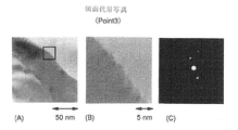
また、後述する実施例4の技術でニッケルのゲッタリング処理を行った本願発明の半導体薄膜を明視野で観察した場合のTEM写真を図19に示す。また、図19中においてPoint 1を30万倍に拡大した写真を図20(A)に、200万倍に拡大した写真を図20(B)に示す。なお、図20(A)内において四角で囲まれた領域が図20(B)に相当する。また、Point 1における電子線回折パターン(スポット径 1.7μmφ)を図20(C)に示す。
【0150】
さらに、Point 1と全く同条件でPoint 2とPoint 3を観察した。Point 2の観察結果を図21(A)、図21(B)、図21(C)に、Point 3の観察結果を図22(A)、図22(B)、図22(C)に示す。
【0151】
これらの観察結果から、任意の結晶粒界において結晶格子に連続性が保たれており、平面状粒界が形成されていることが判る。なお、本出願人はここに示した測定点以外にも多数の領域に渡って観察と測定を繰り返し、TFTを作製するのに十分な広い領域において、結晶粒界における結晶格子の連続性が確保されていることを確認している。
【0152】
〔実施例2〕
実施例1では平坦性に優れた下地を得るために、シリコン基板をハロゲン化物(例えばHCl)を含む雰囲気中で熱酸化する例を示した。本実施例では他の基板を利用する例を示す。
【0153】
本実施例では、まず安価な低級グレードの石英基板を用意する。次に、その石英基板をCMP(化学機械研磨)等の手法により理想状態(凹凸部の差の平均値が5nm以内、代表的には3nm以内、好ましくは2nm以内)にまで研磨する。
【0154】
この様に、安価な石英基板であっても研磨によって優れた平坦性を有する絶縁性基板として利用することができる。石英基板を用いると非常に下地が緻密となるので下地/半導体薄膜界面の安定度が高い。また、基板からの汚染の影響も殆どないので非常に利用価値が高い。
【0155】
〔実施例3〕
実施例1では半導体膜として珪素膜を用いる例を示したが、SiX Ge1-X (0<X<1、好ましくは0.05≦X≦0.95)で示される様にゲルマニウムを1〜10%含有した珪素膜を用いることも有効である。
【0156】
この様な化合物半導体膜を用いた場合、N型TFTおよびP型TFTを作製した際にしきい値電圧を小さくできる。また、電界効果移動度(モビリティと呼ばれる)を大きくすることができる。
【0157】
〔実施例4〕
実施例1では珪素の結晶化を助長する触媒元素をゲッタリングする工程においてハロゲン元素を用いる例を示した。本願発明では、触媒元素のゲッタリング工程にリン元素を用いることも可能である。
【0158】
リン元素を用いる場合、活性層となる領域以外の領域にリンを添加し、 400〜1050℃(好ましくは 600〜750 ℃)の温度で、1min 〜20hr(典型的には30min 〜3hr)の加熱処理を行えば良い。この加熱処理によりリンを添加した領域に触媒元素がゲッタリングされるので、活性層中の触媒元素の濃度は 5×10¹⁷atoms/cm3 以下にまで低減される。
【0159】
こうしてゲッタリング工程を終えたら、リンを添加した領域以外の領域を利用して活性層を形成する。後は、実施例1の工程に従えば実施例1と同じ特徴を有する半導体装置が得られる。
【0160】
勿論、ゲイト絶縁膜となる熱酸化膜を形成する際にハロゲン元素を含む雰囲気中で加熱処理を行えば、本実施例のリン元素によるゲッタリング効果とハロゲン元素によるゲッタリング効果との相乗効果が得られる。
【0161】
〔実施例5〕
本実施例では実施例1に示した半導体装置を利用して反射型液晶パネルを構成する場合の例を示す。図7に示すのはアクティブマトリクス型液晶パネルの断面図であり、ドライバー回路やロジック回路を構成する領域にはCMOS回路を、画素マトリクス回路を構成する領域には画素TFTを示している。
【0162】
CMOS回路はNチャネル型TFTとPチャネル型TFTとを相補的に組み合わせて作製する。CMOS回路を構成する個々のTFTの構成および作製方法は実施例1で説明したので省略する。
【0163】
また、画素TFTはドライバー回路等を構成するTFTにさらに工夫を加える必要がある。図7において701は窒化珪素膜であり、CMOS回路のパッシベーション膜を兼ねると同時に、補助容量を構成する絶縁体として機能する。
【0164】
窒化珪素膜701上にはチタン膜702が形成され、チタン膜702とドレイン電極703との間で補助容量が形成される。この時、絶縁体は比誘電率の高い窒化珪素膜であるので、容量を大きくすることができる。また、反射型では開口率を考慮する必要がないので、図7の様な構造としても問題がない。
【0165】
次に、704は有機性樹脂膜でなる層間絶縁膜であり、本実施例ではポリイミドを用いている。この層間絶縁膜704は膜厚を2μm程度と厚くして十分な平坦性を確保しておくことが好ましい。こうすることで、優れた平坦性を持つ画素電極705を形成することができる。
【0166】
画素電極705はアルミニウムまたはアルミニウムを主成分とする材料で構成する。なるべく反射率の高い材料を用いる方が良い。また、優れた平坦性を確保しておくことで画素電極表面での乱反射損失を低減することができる。
【0167】
画素電極705の上には配向膜706を形成する。配向膜706はラビングによって配向力を持たせる。以上がTFT側基板(アクティブマトリクス基板)の構成に関する説明である。
【0168】
一方、対向基板側は、透過性基板707上に透明導電膜708、配向膜709を形成して構成される。これ以外にも必要に応じてブラックマスクやカラーフィルターを設けることもできる。
【0169】
そして、スペーサ散布、シール材印刷を行った後、液晶層710を封入して図7に示す様な構造の反射型液晶パネルが完成する。液晶層710は液晶の動作モード(ECBモード、ゲストホストモード等)によって自由に選定することができる。
【0170】
また、図7に示した様な反射型液晶パネルを構成するアクティブマトリクス基板の外観を図8に簡略化して示す。図8において、801は実施例1の工程に従って熱酸化膜を設けたシリコン基板、802は画素マトリクス回路、803はソースドライバー回路、804はゲイトドライバー回路、805はロジック回路である。
【0171】
ロジック回路805は広義的にはTFTで構成される論理回路全てを含むが、ここでは従来から画素マトリクス回路、ドライバー回路と呼ばれている回路と区別するため、それ以外の信号処理回路(メモリ、D/Aコンバータ、クロックジェネレータ等)を指す。
【0172】
また、こうして形成された液晶パネルには外部端子としてFPC(Flexible Print Circuit)端子が取り付けられる。一般的に液晶モジュールと呼ばれるのはFPCを取り付けた状態の液晶パネルである。
【0173】
〔実施例6〕
本実施例では実施例1に示した半導体装置を利用して透過型液晶パネルを構成する例を図9に示す。ただし、基本的な構造は実施例4に示した反射型液晶パネルと同じであるので、構成の異なる点を特に説明する。
【0174】
図9に示す透過型液晶パネルの場合、ブラックマスク901の構成が反射型液晶パネルと大きく異なる。即ち、透過型では開口率を稼ぐ必要があるのでTFT部および配線部以外は極力ブラックマスク901が重ならない様な構成とすることが重要である。
【0175】
そのため、本実施例ではTFT部の上にドレイン電極902が重なる様に形成しておき、その上でブラックマスク901との間に補助容量を形成する。この様に、広い面積を占めやすい補助容量をTFTの上に形成することで開口率を広くすることが可能である。
【0176】
また、903は画素電極となる透明導電膜である。透明導電膜903としてはITOが最も多用されるが、他の材料(酸化スズ系など)を用いても良い。
【0177】
本実施例の画素構造において画素TFTの部分に注目した上面図を図23(A)に示す。図23(A)において、51は活性層、52はソース線、53はゲイト線、54はドレイン電極、55はブラックマスク、56はドレイン電極54と画素電極57とを接続するためのコンタクトホールである。
【0178】
本実施例の特徴は、画素TFTの上方においてドレイン電極54とブラックマスク55との間で補助容量を形成する点にある。
【0179】
また、図23(A)をA−A’で示される破線で切断した時に見られる断面構造を図23(B)に示す。なお、図23(A)と図23(B)には共通の符号を用いている。さらに、図23(B)に相当する断面を実際に撮影したTEM写真を図24に示す。
【0180】
この様に、ゲイト線53と重なる様な配置でドレイン電極55が形成され、誘電体58を挟んで対向するブラックマスク55との間に補助容量が形成されている。なお、本実施例ではドレイン電極55としてチタン膜をアルミニウム膜で挟んだ三層構造を採用している。
【0181】
本実施例の場合、ドレイン電極55を形成した後で窒化珪素膜/酸化珪素膜/アクリル膜の三層構造でなる層間絶縁膜を形成し、その上にブラックマスク55を形成する。
【0182】
この時、ブラックマスク55の形成前に、後に補助容量となる領域のアクリル膜のみを除去して開口部を形成しておく。すると、開口部の底には酸化珪素膜と窒化珪素膜しか残らず、この二層構造でなる絶縁層が補助容量の誘電体58として機能するのである。
【0183】
〔実施例7〕
本実施例は、ゲイト電極として導電性を有する珪素膜を用いた、いわゆるシリコンゲイトTFTに適用した場合の例である。基本的な構成は実施例1で作製したTFTとほぼ同様であるので、相違点のみに着目して説明する。
【0184】
図10において、11はNチャネル型TFTのゲイト電極、12はPチャネル型TFTのゲイト電極、13は画素TFTのゲイト電極である。ゲイト電極11〜13はリンまたは砒素を添加したN型ポリシリコン膜、或いはボロンまたはインジウムを添加したP型ポリシリコンを用いる。
【0185】
また、CMOS回路ではNチャネル型TFTにN型ポリシリコンゲイトを用い、Pチャネル型TFTにP型ポリシリコンゲイトを用いたデュアルゲイト型CMOS回路を構成しても良い。
【0186】
この様にゲイト電極として珪素膜を用いる利点としては、耐熱性が高いこと、珪素膜であるので扱いが容易であることなどが挙げられる。また、金属膜との反応を利用してサリサイド構造(ポリサイド構造も含む)をとることができる。
【0187】
そのためには、ゲイト電極11〜13を形成した後にサイドウォール14〜16を形成する。そして、チタン、タングステン等の金属膜(図示せず)を成膜し、加熱処理を行って金属シリサイド17〜19を形成する。金属シリサイド17〜19はソース/ドレイン領域およびゲイト電極の一部に形成される。
【0188】
この様にサイドウォール等を用いて自己整合的に金属シリサイドを形成する構造をサリサイド構造と呼ぶ。この様な構造とすると取り出し電極(ソース/ドレイン電極等)とのオーミック接触が良好なものとなるので有効である。
【0189】
〔実施例8〕
本実施例では非晶質珪素膜の結晶化に際して触媒元素としてゲルマニウムを用いる場合について図16を用いて説明する。まず、基板41として石英基板を用意する。必要に応じて酸化珪素膜等の絶縁膜を下地として設けても良い。
【0190】
次に、非晶質珪素(アモルファスシリコン)膜42を形成する。非晶質珪素膜の成膜は減圧熱CVD法で行い、成膜ガスとしてはジシラン(Si2H6 )を用いる。また、本実施例では非晶質珪素膜の膜厚を75nmとする。
【0191】
次に、非晶質珪素膜42の結晶化工程を行う。本実施例では非晶質珪素膜の結晶化に際して、結晶化を助長する触媒元素としてゲルマニウムを用いる。本実施例の場合、まず成膜した非晶質珪素膜42上にプラズマCVD法によりゲルマニウム膜43を形成する。
【0192】
成膜ガスとしては、ゲルマン(GeH4)ガスを水素又はヘリウムで5〜10倍に希釈したものを用いる。そして、 100〜300 ℃の成膜温度で、20〜50mW/cm2で放電して 1〜50nm(代表的には 10 〜20nm)の膜厚のゲルマニウム膜を成膜することができる。
【0193】
また、ゲルマニウム膜43の成膜方法は減圧熱CVD法で行うことも可能である。ゲルマンは非常に分解しやすいガスであるので、450 ℃程度の低温で容易に分解してゲルマニウム膜を形成することができる。
【0194】
こうして図16(A)の状態が得られる。次に、 450〜650 ℃(好ましくは 500〜550 ℃)の加熱処理を行い、非晶質珪素膜42を結晶化させる。 600℃を上限としたのは、これを超えると自然核発生が増加してしまい、ゲルマニウムを核とした結晶と混在して結晶性が乱れるからである。(図16(B))
【0195】
なお、この結晶化工程はファーネスアニール、ランプアニール、レーザーアニールのいずれの手段を用いても良い。本実施例では形成された膜の均質性を重視してファーネスアニールを用いる。
【0196】
こうして得られた結晶性珪素膜(結晶シリコン膜またはポリシリコン膜)44は 500℃程度の低温で形成されたにも拘わらず、優れた結晶性を有している。
【0197】
次に、結晶性珪素膜44上に残存するゲルマニウム膜を硫酸過水溶液(H2SO4 :H2O2=1:1)で除去した後、結晶シリコン膜44に対して少なくとも前述の結晶化の際の温度よりも高い温度(代表的には 800〜1050℃)での熱処理工程を行う。本実施例ではこの熱処理工程を酸化性雰囲気で行う。(図16(C))
【0198】
なお、本実施例の様にシリコンの結晶化を助長する触媒元素としてゲルマニウムを用いる場合、特にゲルマニウムをゲッタリングして除去する必要はない。ゲルマニウムはシリコンと同族の半導体であり、互いに相性が良いのでシリコンの半導体特性に悪影響を与えないと考えられる。
【0199】
この熱処理工程によって高い結晶性を有する結晶性珪素膜45が形成される。また、結晶性珪素膜45上には熱処理工程によって熱酸化膜46が形成される。この熱酸化膜46はTFT作製時にそのままゲイト絶縁膜として利用することも可能である。
【0200】
なお、ゲルマニウム膜を残したまま熱処理を行うこともできるが、その場合は高い濃度で膜中にゲルマニウムが存在した状態となる。いずれにしてもこの熱処理工程を終えた結晶性珪素膜45中には拡散によって 1×10¹⁴〜 5×10¹⁹atoms/cm3 (代表的には 1×10¹⁵〜 1×10¹⁶atoms/cm3 )の濃度でゲルマニウムが存在する。
【0201】
そのため、本実施例で得られた結晶性珪素膜45の表面近傍はシリコン原子とゲルマニウム原子が置換された結合を多く含み、SiX Ge1-X (0<X<1 )で表されるシリコンゲルマニウム半導体に近い半導体薄膜になると考えられる。
【0202】
この時、本実施例の作製工程では結晶性珪素膜上における酸化シリコンの異常成長が全く起こらないという利点がある。即ち、本実施例のプロセスで形成された結晶シリコン膜45は、酸化性雰囲気中に触れた状態で熱酸化されても酸化シリコンの異常成長が発生しない。
【0203】
本出願人によれば、結晶化の触媒としてニッケルを用いた場合、その後の熱処理条件によっては酸化シリコンの異常成長を生じることが確認されている。これは結晶シリコン膜中に存在するニッケルシリサイドが集中的に酸化されることに起因する。本実施例ではその様な異常成長が起こらないのである。
【0204】
また、さらに図16(C)に示した熱処理工程によって結晶シリコン膜44の内部に存在していた粒内欠陥をほぼ完全に除去することができる。結晶化を終えた状態、即ち図16(B)に示した状態の結晶シリコン膜44は、結晶粒内に多くの欠陥(積層欠陥や転位欠陥など)を含んでいる。ところが、図16(C)の工程後に得られた結晶シリコン膜45は、結晶粒内に殆ど欠陥を含まない。
【0205】
本出願人は、このことについてほぼ実施例1で説明したモデルと同様のことが起こっているのであろうと推測している。ただし、触媒元素にニッケルを用いていないので、欠陥が消滅するのはもっぱら熱酸化によって生じた余剰シリコン原子の影響によるところが大きいと思われる。
【0206】
以上の様に、本実施例の工程を採用することで、結晶性珪素膜の異常酸化が防止されるため結晶性珪素膜の熱処理に際して工程を煩雑にすることがない。また、結晶性珪素膜中の粒内欠陥が除去され、非常に結晶性の高い結晶性珪素膜を得ることができる。
【0207】
なお、結晶化温度以上の温度とは、代表的には 800〜1050℃( 好ましくは 850〜900 ℃)の温度であり、その様な高い温度で熱処理を行う点に特徴がある。この工程では熱酸化機構が粒内欠陥の低減に大きく寄与すると思われるので、熱酸化が起こりやすい条件であることが望ましい。
【0208】
従って、スループットを考えると熱処理の下限温度は 800℃が好ましく、上限は基板(本実施例では石英)の耐熱性を考慮して 1050 ℃が好ましい。ただし、ゲルマニウムの融点が 930〜940 ℃であるので、より好ましくは 900℃を上限とすると良い。
【0209】
また、熱処理雰囲気は酸化性雰囲気であることが好ましいが、不活性雰囲気であっても構わない。酸化性雰囲気とする場合、ドライ酸素(O2)雰囲気、ウェット酸素(O2+H2)雰囲気、ハロゲン元素を含む雰囲気(O2+HCl 等)のいずれかとすれば良い。
【0210】
特に、ハロゲンを含む雰囲気で熱処理を行うと、ハロゲン元素のゲッタリング効果により結晶性珪素膜の格子間に存在する余分なゲルマニウムが揮発性のGeCl4 の形で除去される。そのため、格子歪みの少ない結晶性珪素膜を得るためには有効な手段である。
【0211】
なお、本実施例は他のどの実施例とも組み合わせることができる。
【0212】
〔実施例9〕
本願発明のTFTは実質的に単結晶と見なせる半導体薄膜を活性層として利用しているため、単結晶シリコンを用いたMOSFETに匹敵する電気特性を示す。本発明者らが試作したTFTからは次に示す様なデータが得られている。
【0213】
(1)TFTのスイッチング性能(オン/オフ動作の切り換えの俊敏性)の指標となるサブスレッショルド係数が、Nチャネル型TFTおよびPチャネル型TFTともに60〜100mV/decade(代表的には60〜85mV/decade )と小さい。
(2)TFTの動作速度の指標となる電界効果移動度(μFE)が、Nチャネル型TFTで200 〜650cm2/Vs (代表的には250 〜300cm2/Vs )、Pチャネル型TFTで100 〜300cm2/Vs (代表的には150 〜200cm2/Vs )と大きい。
(3)TFTの駆動電圧の指標となるしきい値電圧(Vth)が、Nチャネル型TFTで-0.5〜1.5 V、Pチャネル型TFTで-1.5〜0.5 Vと小さい。
【0214】
以上の様に、本発明で得られるTFTは極めて優れたスイッチング特性および高速動作特性を有している。そのため、これまでMOSFETで構成されてきたLSIなどの集積化回路をTFTで構成することが可能となる。
【0215】
さらには、薄膜を用いるTFTの利点を生かして三次元構造の半導体装置(半導体回路)を構成することも可能となる。
【0216】
図11に示す半導体回路は、本願発明のTFTを用いた三次元構造の半導体回路の一例を示している。図11(A)は下側にTFT層、上側にイメージセンサを積層した三次元回路である。また、図11(B)は上層及び下層にTFT層を配置した三次元回路である。
【0217】
図11(A)において、21は光電変換層であり非晶質珪素膜等を用いることができる。その上には上部電極(透明導電膜)22が設けられ、光を受光して電気信号に変換する受光部を構成している。
【0218】
なお、TFTの作製行程は実施例1で既に説明したので省略する。また、三次元回路を構成するための積層技術は、公知の手段を用いれば良い。ただし、上側のTFT層を形成する場合、下層のTFTの耐熱性を考慮する必要がある。
【0219】
例えば、下層を本願発明のTFTで構成し、上層を従来の低温形成のTFTとする構成でも良い。また、下層のTFTを耐熱性の高い材料で形成しておき、上層に本願発明のTFTを形成する様な構造としても良い。
【0220】
また、上層となるイメージセンサは受光部だけで構成した下層のTFTで上層の受光部を制御する構成としても良い。
【0221】
次に、図11(B)において、下層はシリコンゲイト構造を用いたTFT層であり、上層はシリコンゲイト構造または他の金属膜(アルミニウムを主成分とする膜等)をゲイト電極として用いた構造のTFT層である。なお、図11(B)もTFT構造の説明は省略する。
【0222】
この様な構造においても、上層のTFTを形成する際に下層のTFTの耐熱性を十分の考慮した上で作製することが必要である。
【0223】
また、図11(A)、(B)のどちらも、下層のTFTを形成した後に厚めに層間絶縁膜23、24を形成し、それをCMP(化学機械研磨)等で研磨して平坦化した後に上層のTFTを形成することが望ましい。
【0224】
以上の様に、本願発明のTFTを用いて三次元構造の半導体回路を構成することで、非常に機能性に富んだ半導体回路を構成することが可能である。なお、本明細書中において、半導体回路とは半導体特性を利用して電気信号の制御、変換を行う電気回路という意味で用いている。
【0225】
また、本願発明のTFTを用いてLCDドライバ回路や携帯機器用の高周波回路(MMIC:マイクロウェイブ・モジュール・IC)などを構成することもできる。即ち、本願発明のTFTを用いることで従来のICチップやLSIチップをTFTで作製することが可能である。
【0226】
〔実施例10〕
本願発明は液晶表示装置以外にも、アクティブマトリクス型のEL(エレクトロルミネッセンス)表示装置やEC(エレクトロクロミクス)表示装置等の他の電気光学装置を作製することも可能である。また、イメージセンサやCCDを作製することも可能である。
【0227】
なお、電気光学装置とは電気信号を光学的信号に変換する装置またはその逆を行う装置という意味で用いている。
【0228】
〔実施例11〕
本実施例では、本発明を利用した電気光学装置を利用する電子機器(応用製品)の一例を図12に示す。なお、電子機器とは半導体回路および/または電気光学装置を搭載した製品のことを意味している。
【0229】
本願発明を適用しうる電子機器としてはビデオカメラ、電子スチルカメラ、プロジェクター、ヘッドマウントディスプレイ、カーナビゲーション、パーソナルコンピュータ、携帯情報端末(モバイルコンピュータ、携帯電話、PHS(パーソナルハンディフォンシステム)等)などが挙げられる。
【0230】
図12(A)は携帯電話であり、本体2001、音声出力部2002、音声入力部2003、表示装置2004、操作スイッチ2005、アンテナ2006で構成される。本願発明は音声出力部2002、音声出力部2003、表示装置2004等に適用することができる。
【0231】
図12(B)はビデオカメラであり、本体2101、表示装置2102、音声入力部2103、操作スイッチ2104、バッテリー2105、受像部2106で構成される。本願発明は表示装置2102、音声入力部2103、受像部2106等に適用することができる。
【0232】
図12(C)はモバイルコンピュータ(モービルコンピュータ)であり、本体2201、カメラ部2202、受像部2203、操作スイッチ2204、表示装置2205で構成される。本願発明はカメラ部2202、受像部2203、表示装置2205等に適用できる。
【0233】
図12(D)はヘッドマウントディスプレイであり、本体2301、表示装置2302、バンド部2303で構成される。本発明は表示装置2302に適用することができる。
【0234】
図12(E)はリア型プロジェクターであり、本体2401、光源2402、表示装置2403、偏光ビームスプリッタ2404、リフレクター2405、2406、スクリーン2407で構成される。本発明は表示装置2403に適用することができる。
【0235】
図12(F)はフロント型プロジェクターであり、本体2501、光源2502、表示装置2503、光学系2504、スクリーン2505で構成される。本発明は表示装置2503に適用することができる。
【0236】
以上の様に、本願発明の適用範囲は極めて広く、あらゆる分野の電子機器に適用することが可能である。また、電気光学装置や半導体回路を必要とする製品であれば全てに適用できる。
【0237】
【発明の効果】
本明細書で開示する発明によれば、実質的に単結晶と見なせる結晶性を有する半導体薄膜を形成することができる。そして、その様な半導体薄膜を利用することで単結晶上に作製したMOSFETに匹敵する、或いは凌駕しうる高い性能を有したTFTを実現することができる。
【0238】
以上の様なTFTを用いて構成される半導体回路や電気光学装置およびそれらを搭載した電子機器は、極めて高い性能を有し、機能性、携帯性、信頼性の面で非常に優れた製品となる。
【図面の簡単な説明】
【図1】 半導体薄膜の電子回折パターンを示す写真。
【図2】 電子線回折パターンを模式的に表した図。
【図3】 半導体薄膜の方位関係を説明するための図。
【図4】 結晶粒界の形態を示す図。
【図5】 半導体装置の作製工程を示す図。
【図6】 半導体装置の作製工程を示す図。
【図7】 電気光学装置の断面を示す図。
【図8】 アクティブマトリクス基板の外観を示す図。
【図9】 アクティブマトリクス基板の断面を示す図。
【図10】 アクティブマトリクス基板の断面を示す図。
【図11】 半導体回路の一例を示す図。
【図12】 電子機器の一例を示す図。
【図13】 SIMS測定結果を示す図。
【図14】 結晶シリコン膜の結晶粒を示すTEM写真。
【図15】 欠陥の生成および消滅に関するモデルを説明するための図。
【図16】 半導体装置の作製工程を示す図。
【図17】 半導体薄膜の結晶粒を示すTEM写真。
【図18】 半導体薄膜の暗視野像を示すTEM写真。
【図19】 半導体薄膜の明視野像を示すTEM写真。
【図20】 半導体薄膜の結晶粒界の様子を示すTEM写真。
【図21】 半導体薄膜の結晶粒界の様子を示すTEM写真。
【図22】 半導体薄膜の結晶粒界の様子を示すTEM写真。
【図23】 画素TFTの上面及び断面構造を示す図。
【図24】 画素TFTの断面構造を示すTEM写真。[0001]
[Technical field to which the invention belongs]
The invention disclosed in this specification relates to a semiconductor thin film formed over a substrate having an insulating surface and a semiconductor device using the semiconductor thin film as an active layer. In particular, the present invention relates to a configuration in which a material containing silicon (silicon) as a main component is used as a semiconductor thin film.
[0002]
In addition, the present invention relates to the configuration of a semiconductor circuit and an electro-optical device that are configured by a semiconductor device such as a thin film transistor, and an electronic device in which they are mounted.
[0003]
Note that in this specification, the above thin film transistors, semiconductor circuits, electro-optical devices, and electronic devices are all included in the category of “semiconductor devices”. That is, all devices that can function using semiconductor characteristics are called semiconductor devices. Therefore, the semiconductor device described in the claims includes not only a single element such as a thin film transistor but also a semiconductor circuit or an electro-optical device in which the semiconductor device is integrated, and an electronic device in which they are mounted as components.
[0004]
[Prior art]
In recent years, a technique for forming a thin film transistor (TFT) using a semiconductor thin film (having a thickness of about several tens to several hundreds nm) formed on a substrate having an insulating surface has attracted attention. Thin film transistors are particularly urgently developed as switching elements for image display devices (for example, liquid crystal display devices).
[0005]
For example, in a liquid crystal display device, a pixel matrix circuit that individually controls pixel areas arranged in a matrix, a drive circuit that controls the pixel matrix circuit, and a logic circuit (arithmetic circuit, memory circuit) that processes an external data signal Attempts have been made to apply TFTs to various electric circuits such as clock generators.
[0006]
At present, TFTs using an amorphous silicon film (amorphous silicon film) as an active layer have been put into practical use. However, electrical circuits that require higher-speed operation performance, such as drive circuits and logic circuits, are used. A TFT using a crystalline silicon film (polysilicon film or the like) is required.
[0007]
For example, as a method for forming a crystalline silicon film on a glass substrate, techniques described in Japanese Patent Application Laid-Open Nos. 7-130652 and 8-78329 by the present applicant are known. The technologies described in these publications form a crystalline silicon film having excellent crystallinity by heating at 500 to 600 ° C. for about 4 hours by using a catalytic element that promotes crystallization of the amorphous silicon film. It is possible to do.
[0008]
In particular, the technique described in Japanese Patent Application Laid-Open No. 8-78329 applies the above technique to perform crystal growth substantially parallel to the substrate surface. Or a lateral growth region).
[0009]
However, even if a drive circuit is configured using such TFTs, the required performance is still not fully satisfied. In particular, it is currently impossible to construct a high-speed logic circuit that requires extremely high-speed operation from megahertz to gigahertz using conventional TFTs.
[0010]
[Problems to be solved by the invention]
The present inventors have repeated various thoughts and errors so far in order to improve the crystallinity of a crystalline silicon film having crystal grain boundaries (referred to as a polysilicon film). Examples thereof include semi-amorphous semiconductors (Japanese Patent Laid-Open No. 57-160121, etc.) and monodomain semiconductors (Japanese Patent Laid-Open No. 8-39019, etc.).
[0011]
The concept common to the semiconductor films described in the above publication is to make the grain boundaries substantially harmless. That is, the biggest problem is to substantially eliminate crystal grain boundaries and to smoothly move carriers (electrons or holes).
[0012]
However, even with the semiconductor film described in the above publication, it can be said that it is insufficient for the high-speed operation required by the logic circuit. In other words, in order to realize a system-on-panel with a built-in logic circuit, development of a completely new material that has not been heretofore required is required.
[0013]
The present invention responds to such a demand, and provides a semiconductor thin film for realizing an extremely high performance semiconductor device capable of constituting a high-speed logic circuit that cannot be manufactured by a conventional TFT. Is an issue. Another object is to provide a semiconductor device using such a semiconductor thin film.
[0014]
[Means for Solving the Problems]
The configuration of the invention disclosed in this specification is as follows.
A semiconductor thin film comprising an assembly of a plurality of rod-like or flat rod-like crystals mainly composed of silicon,
The main orientation plane is roughly the {110} plane,
The concentration of C (carbon) and N (nitrogen) present in the film is 5 × 10 17 atoms / cm Three Below, the concentration of O (oxygen) is 1 × 10 18 atoms / cm Three And
The plurality of rod-like or flat rod-like crystals are in contact with each other with a rotation angle, and the absolute value of the rotation angle is within 3 °.
[0015]
Further, in the above configuration, specific regularity due to {110} orientation is observed in the electron beam diffraction pattern of the semiconductor thin film,
Arbitrary diffraction spots of the electron beam diffraction pattern are approximately circular,
The ratio (a / b) of the minor axis length (a) to the major axis length (b) of the diffraction spot is from 1/1 (circular) to 1 / 1.5.
[0016]
Further, in the above configuration, specific regularity due to {110} orientation is observed in the electron beam diffraction pattern of the semiconductor thin film,
An arbitrary diffraction spot of the electron beam diffraction pattern has a concentric expanse with respect to the center point of the electron beam irradiation area,
The angle formed by the tangent drawn to the diffraction spot from the center point of the electron beam irradiation area and the line segment connecting the center point of the electron beam irradiation area and the center point of the diffraction spot is within ± 1.5 °. It is characterized by being.
[0017]
The present invention having the above-described configuration will be described in detail with the following examples.
[0018]
【Example】
[Example 1]
In this embodiment, a manufacturing process of a semiconductor thin film according to the present invention and a semiconductor device (specifically, a TFT) using the semiconductor thin film as an active layer will be described.
[0019]
First, a
[0020]
The
[0021]
Thus, a substrate having a very flat insulating surface as shown in FIG. 5A is obtained. This excellent flatness plays an important role in forming the semiconductor thin film of the present invention.
[0022]
Next, an
It is important to thoroughly control the impurity concentration in the film during film formation. In the case of this embodiment, the concentrations of C (carbon) and N (nitrogen), which are impurities that inhibit crystallization, in the
[0024]
FIG. 13 shows the result of examining the impurity concentration in the amorphous silicon film manufactured under the conditions of this example by SIMS (mass secondary ion analysis). The sample used was an amorphous silicon film having a thickness of 0.5 μm formed on a silicon wafer. As a result, as shown in FIG. 13, it was confirmed that all elements of C, N, and O were within the above concentration range. However, in this specification, the element concentration in the film is defined by the minimum value in the SIMS measurement result.
[0025]
In order to obtain the above-described configuration, it is desirable that the low-pressure thermal CVD furnace used in this embodiment periodically perform dry cleaning to clean the film formation chamber. Dry cleaning is performed in a furnace heated to about 200 to 400 ° C. and 100 to 300 sccm of ClF. Three A (chlorine fluoride) gas is allowed to flow, and the film formation chamber may be cleaned with fluorine generated by thermal decomposition.
[0026]
According to the knowledge of the present inventors, the furnace temperature was set to 300 ° C., and ClF Three When the flow rate of (chlorine fluoride) gas is set to 300 sccm, deposits having a thickness of about 2 μm (mainly containing silicon as a main component) can be completely removed in 4 hours.
[0027]
Further, the hydrogen concentration in the
[0028]
Next, a crystallization process of the
[0029]
In the technique described in Japanese Patent Laid-Open No. 8-78329, first, a
[0030]
In addition to nickel, the catalytic element is cobalt (Co), iron (Fe), palladium (Pd), platinum (Pt), copper (Cu), gold (Au), germanium (Ge), lead (Pb). Indium (In) or the like can be used.
[0031]
The catalyst element addition step is not limited to the spin coating method, and an ion implantation method or a plasma doping method using a resist mask can also be used. In this case, since the occupied area of the added region can be reduced and the growth distance of the lateral growth region can be easily controlled, this is an effective technique for configuring a miniaturized circuit.
[0032]
Next, after the catalyst element addition process is completed, after dehydrogenation at 450 ° C. for about 1 hour, a temperature of 500 to 700 ° C. (typically 550 to 650 ° C.) in an inert atmosphere, hydrogen atmosphere or oxygen atmosphere The
[0033]
At this time, the crystallization of the
[0034]
When the heat treatment for crystallization is completed, the
[0035]
Next, as shown in FIG. 5D, heat treatment (catalyst element gettering process) for removing or reducing the catalyst element (nickel) is performed. In this heat treatment, a halogen element is included in the treatment atmosphere, and the gettering effect of the metal element by the halogen element is used.
[0036]
Note that the heat treatment is preferably performed at a temperature exceeding 700 ° C. in order to sufficiently obtain the gettering effect by the halogen element. Below this temperature, decomposition of the halogen compound in the processing atmosphere becomes difficult, and the gettering effect may not be obtained. Therefore, the heat treatment temperature is preferably 800 to 1000 ° C. (typically 950 ° C.), and the treatment time is 0.1 to 6 hr, typically 0.5 to 1 hr.
[0037]
As a typical example, heating is performed at 950 ° C. for 30 minutes in an atmosphere containing hydrogen chloride (HCl) at a concentration of 0.5 to 10% by volume (in this example, 3% by volume) with respect to an oxygen atmosphere. What is necessary is just to process. If the HCl concentration is equal to or higher than the above concentration, the surface of the
[0038]
In addition, as a compound containing a halogen element, HF, NF other than HCl gas Three , HBr, Cl 2 , ClF Three , BCl Three , F 2 , Br 2 One or a plurality of compounds selected from compounds containing a halogen element such as the above can be used.
[0039]
In this step, nickel in the
[0040]
The gettering process is also effective for metal elements other than nickel. As the metal elements that can be mixed into the silicon film, the constituent elements of the deposition chamber (typically aluminum, iron, chromium, etc.) can be considered, but if the gettering process is performed, the concentration of these metal elements is considered. Also 5 × 10 17 atoms / cm Three Below (preferably 2 × 10 17 atoms / cm Three The following is possible:
[0041]
When the gettering process is performed, the
[0042]
Further, the heat treatment causes a thermal oxidation reaction to proceed at the interface between the
[0043]
It is also effective to improve the film quality of the
[0044]
Note that this gettering step using a halogen element can also be performed between the crystallization step and the gate insulating film formation step.
[0045]
Next, a metal film (not shown) containing aluminum as a main component is formed, and a
[0046]
Here, the technique described in Japanese Patent Laid-Open No. 7-13518 by the present inventors is used. This publication discloses a technique for forming source / drain regions and low-concentration impurity regions in a self-aligning manner using an oxide film formed by anodic oxidation. The technique will be briefly described below.
[0047]
First, a porous
[0048]
Next, after removing a resist mask (not shown), anodization is performed in an electrolytic solution in which 3% tartaric acid is mixed with an ethylene glycol solution. In this process, a dense non-porous
[0049]
The
[0050]
Next, the
[0051]
Next, an impurity element adding step for imparting one conductivity is performed. As the impurity element, P (phosphorus) or As (arsenic) may be used for N type, and B (boron) or In (indium) may be used for P type.
[0052]
In this step, first impurity addition is performed at a high acceleration voltage, and n - Form a region. At this time, since the acceleration voltage is as high as about 80 keV, the impurity element is added not only to the exposed active layer surface but also under the exposed end portion of the gate insulating film. Further, the second impurity addition is performed at a low acceleration voltage, and n + Form a region. At this time, since the acceleration voltage is as low as about 10 keV, the gate insulating film functions as a mask.
[0053]
The impurity region formed by the above steps is n + The regions become a
[0054]
When the active layer is completed as described above, the impurity element is activated by a combination of furnace annealing, laser annealing, lamp annealing and the like. At the same time, the damage of the active layer received in the addition process is also repaired.
[0055]
Next, an interlayer insulating film 519 is formed to a thickness of 500 nm. As the interlayer insulating film 519, a silicon oxide film, a silicon nitride film, a silicon oxynitride film, an organic resin film, or a stacked film thereof can be used.
[0056]
Next, after forming contact holes, a
[0057]
In addition, since this invention is a technique regarding the semiconductor thin film which comprises an active layer, other structures and structures do not limit this invention at all. Therefore, the present invention can be easily applied to TFTs having structures and configurations other than the present embodiment.
[0058]
(Knowledge about impurities contained in active layer)
The active layer (semiconductor thin film) of this embodiment is characterized in that C (carbon), N (nitrogen), and O (oxygen), which are elements that inhibit crystallization, are not present or substantially absent. This is a configuration that can be achieved through thorough impurity (contamination) management.
[0059]
In the case of the present embodiment, since the mixing of C (carbon), N (nitrogen) and O (oxygen) is thoroughly avoided in the formation of the amorphous silicon film, it inevitably exists in the final semiconductor film. The concentration of C (carbon) and N (nitrogen) is at least 5 × 10 18 atoms / cm Three Less than (typically 5x10 17 atoms / cm Three Below, preferably 2 × 10 17 atoms / cm Three Below), O (oxygen) concentration is at least 1.5 × 10 19 atoms / cm Three Less than (typically 1x10 18 atoms / cm Three Below, preferably 5 × 10 17 atoms / cm Three The following.
[0060]
In the case of a semiconductor film made of pure silicon, the silicon concentration is about 5 × 10 twenty two atoms / cm Three So, for example, 5 × 10 18 atoms / cm Three This corresponds to the presence of the impurity element at a concentration of about 0.01 atomic%.
[0061]
In addition, it is desirable that the concentration of C (carbon), N (nitrogen), and O (oxygen) present in the final semiconductor film is less than the lower limit of detection in SIMS analysis, and more preferably not completely present. It is necessary to obtain high crystallinity.
[0062]
As a result of analysis by the SIMS by the present inventors, when an amorphous silicon film in which the concentrations of C, N, and O all satisfy the above concentration range is used as a starting film, C contained in the active layer of the completed TFT It has been found that the concentrations of N, O also satisfy the above concentration range.
[0063]
[Knowledge about the crystal structure of the active layer]
When viewed microscopically, the active layer formed in accordance with the above manufacturing process has a crystal structure in which a plurality of rod-shaped (or flat rod-shaped) crystals are arranged in parallel to each other with regularity in a specific direction. This can be easily confirmed by observation with a TEM (transmission electron microscope).
[0064]
Here, FIG. 17 shows an HR-TEM photograph in which the grain boundary between rod-like or flat rod-like crystals is enlarged 8 million times. In the present specification, a crystal grain boundary is defined as a grain boundary formed at a boundary where a rod-shaped or flat rod-shaped crystal is in contact. Therefore, for example, it is considered to be distinguished from a grain boundary in a macro sense such that the laterally grown regions collide with each other.
[0065]
By the way, the above-mentioned HR-TEM (High Resolution Transmission Electron Microscopy) is a method in which an electron beam is irradiated perpendicularly to a sample and the atomic / molecular arrangement is evaluated using interference of transmitted electrons and elastically scattered electrons. It is.
[0066]
In HR-TEM, it is possible to observe the arrangement state of crystal lattices as lattice fringes. Therefore, by observing the crystal grain boundary, it is possible to infer the bonding state between atoms at the crystal grain boundary. Note that the lattice stripes appear as white and black stripes, but they are different in contrast and do not indicate the position of atoms.
[0067]
FIG. 17A is a typical TEM photograph of the crystalline silicon film obtained in the present invention, in which two different crystal grains are in contact with each other at the grain boundary seen from the upper left to the lower right of the photograph. . At this time, the two crystal grains had a roughly {110} orientation although the crystal axes included some deviation.
[0068]
As will be described later, as a result of examining a plurality of crystal grains, it has been confirmed by X-ray diffraction and electron beam diffraction that almost all have a substantially {110} orientation. Although many (011) planes and (200) planes should be present in many observations, these equivalent planes are collectively expressed as {110} planes.
[0069]
Incidentally, as shown in FIG. 17A, lattice fringes corresponding to the {111} plane and the {100} plane are observed in the plane. Note that the lattice stripe corresponding to the {111} plane refers to a lattice stripe such that a {111} plane appears in a cross section when crystal grains are cut along the lattice stripe. It can be simply confirmed from the interval between the lattice fringes what surface the lattice fringes correspond to.
[0070]
Note that the difference in the appearance of lattice fringes in FIG. 17A is due to a subtle difference in the inclination of crystal grains. That is, if the electron beam is set to be perpendicular to the crystal plane of one of the crystal grains, the other crystal grain is slightly irradiated with the electron beam, so the appearance of the lattice fringes changes. is there.
[0071]
Here, attention is paid to lattice fringes corresponding to the {111} plane. In FIG. 17A, the lattice stripe corresponding to the {111} plane of the upper crystal grain across the grain boundary is approximately 70 ° (exactly 70.5 ° to the lattice stripe corresponding to the {111} plane of the lower crystal grain. ).
[0072]
Such a crystal structure (exactly, the structure of the crystal grain boundary) indicates that two different crystal grains are joined with extremely good consistency at the crystal grain boundary. That is, the crystal lattice is continuously connected at the crystal grain boundary, and the trap level caused by crystal defects or the like is very difficult to create. In other words, it can be said that the crystal lattice has continuity at the grain boundaries.
[0073]
For reference, an HR-TEM photograph of a conventional high-temperature polysilicon film is shown in FIG. In the case of FIG. 17B, as will be described later, there is no regularity in the crystal plane, and the {110} plane is not the main orientation. However, here, for comparison with FIG. 17A, crystal grains in which lattice fringes corresponding to the {111} plane appear were observed.
[0074]
When FIG. 17B is observed in detail, as indicated by arrows in the figure, many portions where lattice fringes are interrupted can be confirmed at the crystal grain boundary. In such a portion, a dangling bond (which can be called a crystal defect) is present, and there is a high possibility of inhibiting the movement of carriers as a trap level.
[0075]
However, there is certainly a dangling bond as shown in FIG. 17B in the crystalline silicon film of the present invention. This is because the crystalline silicon film of the present invention is only polycrystalline. However, as a result of TEM observation of the crystalline silicon film of the present invention over a wide range in detail, it has been found that such dangling bonds are very few.
[0076]
As far as the present applicant has examined, continuity of crystal lattices can be seen at 90% or more (typically 95% or more) of the crystal grain boundaries, and unbonded hands as shown in FIG. Could hardly be found. From this fact, it can be said that the crystalline silicon film of the present invention is a semiconductor film that is clearly different from the conventional high-temperature polysilicon.
[0077]
Next, the result of examining the semiconductor thin film of the present invention by electron diffraction is shown in FIG. FIG. 1B shows an electron diffraction pattern of a conventional high-temperature polysilicon film as a reference. 1A and 1B, the diameters of the electron beam irradiation areas are 4.25 μm and 1.35 μm, respectively. In this example, a representative photograph of a plurality of points measured is shown.
[0078]
In the case of FIG. 1A, diffraction spots (diffraction spots) corresponding to <110> incidence appear relatively cleanly, and almost all crystal grains are {110} oriented in the electron beam irradiation area. Can be confirmed.
[0079]
The present applicant performed X-ray diffraction according to the method described in JP-A-7-321339, and calculated the orientation ratio of the semiconductor thin film of the present invention. In this publication, the orientation ratio is defined by a calculation method as shown in the following equation (1).
[0080]
[Expression 1]
As a result of examining the orientation of the semiconductor thin film of the present invention by X-ray diffraction, a peak corresponding to the (220) plane appeared in the X-ray diffraction pattern. Of course, it goes without saying that (220) is equivalent to {110}. As a result of this measurement, it was found that the {110} plane is the main orientation plane, and the orientation ratio is 0.7 or more (typically 0.9 or more).
[0082]
On the other hand, in the case of the conventional high-temperature polysilicon film shown in FIG. 1B, no clear regularity is observed in the diffraction spot, and the orientation is almost random, in other words, a plane orientation other than the {110} plane. It has been found that the crystal grains are irregularly mixed.
[0083]
Note that each diffraction spot has a slight concentric spread, which is presumed to have a certain degree of rotation angle distribution around the crystal axis. This will be described below.
[0084]
A part of the electron beam diffraction pattern shown in FIG. 1A is schematically shown in FIG. In FIG. 2A, a plurality of volatile points denoted by 201 are diffraction spots corresponding to <110> incidence. The plurality of
[0085]
Here, an enlarged view of the
[0086]
That is, an angle (rotation) formed by a
[0087]
This tendency can be seen in the entire region of the electron diffraction pattern shown in FIG. 1A, and is within ± 2.5 ° as a whole (typically within ± 1.5 °, preferably within ± 0.5 °). The term “each diffraction spot has a slight concentric extent” refers to this.
[0088]
Further, by making the base of the semiconductor thin film as flat as possible, the ratio (a / b) of the minor axis length (a) to the major axis length (b) of the
[0089]
In order for the diffraction spot to be circular, the rotation angle existing between a plurality of crystal grains must be made very small. Considering that the diffraction spot is completely circular in the electron diffraction pattern of a single crystal, the fact that the diffraction spot is circular is nothing but the semiconductor thin film of the present invention is as close as possible to the single crystal.
[0090]
FIG. 3A shows the relationship between the crystal axis when the plane orientation is {110} and the axis included in the crystal plane. Thus, if the crystal plane is in the {110} orientation, the crystal axis is the <110> axis, and the <111> axis, the <100> axis, and the like are included in the crystal plane.
[0091]
Further, as a result of the inventors previously examining the growth direction of the rod-like crystal using HR-TEM, it has been confirmed that the rod-like crystal grows in the direction of the <111> axis (Japanese Patent Laid-Open No. 7-321339). No. publication). Therefore, it is considered that a part of the semiconductor thin film of the present invention is enlarged as shown in FIG.
[0092]
In FIG. 3B,
[0093]
At this time, if the <111>
[0094]
It should be noted that the above-mentioned diffraction spot spread is within ± 2.5 ° (typically within ± 1.5 °, preferably within ± 0.5 °). In other words, the absolute value of the rotation angle is within 5 °. (Typically within 3 °, preferably within 1 °).
[0095]
When this relationship is easily understood in FIG. 3C, in the semiconductor thin film of the present invention, the angle (α) between the
[0096]
Then, individual crystal grains having a delicate rotation angle as shown in FIG. 3B appear on the electron diffraction pattern as different diffraction spots. For example, the diffraction spots of the
[0097]
That is, if there are a plurality of crystal grains in the electron beam irradiation area, diffraction spots corresponding to the plurality of crystal grains are continuously arranged on a concentric circle, and the diffraction spots appear to have a shape close to an ellipse. As shown. This is the reason why the spread of diffraction spots was observed in the electron diffraction pattern of FIG.
[0098]
In this embodiment, <111> and the like are described, but this includes a plurality of equivalent axes such as [111] and [1-11] (a minus sign means inversion). . That is, diffraction spots appear corresponding to all the equivalent axes, and as a result, an electron beam diffraction pattern as shown in FIG. 1A is formed. Therefore, if the crystal grains are rotated by the rotation angle, electron beam diffraction is performed. The pattern also rotates as much as the rotation angle. Therefore, all diffraction spots have a concentric circle.
[0099]
As described above, as a result of examining the semiconductor thin film of the present invention by electron beam diffraction, the diffraction pattern as shown in FIG. 1A was obtained because a plurality of rod-like crystals exist in the electron beam irradiation area. , Each having a slightly different rotation angle. Further, the absolute value of the rotation angle is considered to be within 5 ° (typically within 3 °, preferably within 1 °) from the extent of the diffraction spot.
[0100]
This means that the deviation of any reference axis is within at least 5 ° between the two crystal grains having the largest rotation angle among all the crystal grains constituting the semiconductor thin film of the present invention. ing.
[0101]
Here, the presence of various crystal grain boundaries in the semiconductor thin film of the present invention will be described by taking over the classification of crystal grain boundaries generally performed. The following table considers data relating to the semiconductor thin film of the present invention.
[0102]
[Table 1]
In addition, the crystal grain boundary of the form shown in Table 1 can be identified by making full use of electron diffraction, HR-TEM, cross-sectional TEM, and more detailed information can be obtained. In addition, the value of the rotation angle handled in this specification is measured by analyzing the crystal grain boundary from various angles by combining the above methods.
[0104]
Since the rotation about the crystal axis is “rotation about the orientation included in the grain interface”, it is included in the low-inclination grain boundary. When such a crystal grain boundary is formed, the two crystal grains are in contact with each other in a relation as shown schematically in FIG. In this case, the surface where the two crystal grains contact is the grain interface. However, since the rotation angle around the crystal axis is as small as ± 2.5 ° in the semiconductor thin film of the present invention, it can be considered that there are almost no grain boundaries as shown in FIG. .
[0105]
Further, there are cases where the low-inclination grain boundary is as shown in FIG. In the case of the form of FIG. 4 (B), the axis | shaft used as a rotating shaft differs from FIG. 4 (A). However, the point that the two crystal grains have a certain rotation angle about the axis included in the grain interface is the same as in FIG. 4A. In the semiconductor thin film of the present invention, since the rotation angle in this case is also within ± 2.5 ° (typically within ± 1.5 °, preferably within 0.5 °), it is considered that such a crystal grain boundary hardly exists. Can do.
[0106]
Further, although distinguished from the small-angle grain boundaries shown in FIGS. 4A and 4B, there is a form called a twist grain boundary in the same low-angle grain boundary classification. As shown in FIG. 4C, this corresponds to the case of rotating about an orientation perpendicular to the grain interface.
[0107]
In this case as well, the point that the two crystal grains have a certain rotation angle is the same as that of the low-inclination grain boundary. In the semiconductor thin film of the present invention, the rotation angle is within ± 2.5 ° (typically within ± 1.5 °). , Preferably within 0.5 °). That is, it can be considered that there is almost no twist grain boundary.
[0108]
As described above, it is considered that the semiconductor thin film of the present invention has no or substantially no electrically active crystal grain boundary generally called a low angle grain boundary. Note that “electrically active” means that the carrier can function as a trap.
[0109]
In addition, “substantially no” means, for example, that when a crystal grain boundary included in a range of 5 μm square is examined, the corresponding grain boundary (for example, a low-angle grain boundary) is one or two even if observed. Refers to a certain case.
[0110]
In addition, there are twin grain boundaries and other corresponding grain boundaries in special high-angle grain boundaries, and it has been confirmed that most of the semiconductor thin films of the present invention are twin grain boundaries. Even if this corresponding grain boundary exists, it has been found that it is electrically inactive (does not function as a carrier trap).
[0111]
In particular, in the semiconductor thin film of the present invention, the corresponding grain boundary ({111} twin grain boundary) of Σ3 occupies 90% or more (typically 95% or more) of the whole, and the crystal grain boundary with very good consistency. It is proved in a wide range that is formed.
[0112]
The Σ value is a parameter that serves as a guideline indicating the degree of matching of the corresponding grain boundary, and it is known that the smaller the Σ value, the better the grain boundary. The definition of Σ value is detailed in “High-resolution electron microscopy for material evaluation; Daisuke Shindo, Kenji Hiraga, pp.54-60, Kyoritsu Shuppan Co., Ltd., 1996”.
[0113]
In the crystal grain boundary formed between two crystal grains, when the plane orientation of both crystals is {110}, assuming that the angle formed by the lattice stripes corresponding to the {111} plane is θ, θ = 70.5 ° It is known that sometimes it becomes the corresponding grain boundary of Σ3.
[0114]
Therefore, in the crystal grain boundary shown in the TEM photograph of FIG. 1A, each lattice stripe of adjacent crystal grains is continuous at an angle of 70.5 °, and this crystal grain boundary is a {111} twin crystal grain boundary. It can be easily guessed that there is.
[0115]
Incidentally, when θ = 38.9 °, the corresponding grain boundary of Σ9 is obtained, but there are some other corresponding grain boundaries.
[0116]
Such a corresponding grain boundary is formed only between crystal grains having the same plane orientation. That is, because the semiconductor thin film of the present invention has a plane orientation of approximately {110}, such a corresponding grain boundary can be formed over a wide range. This feature is not possible with other polysilicon films with irregular surface orientation.
[0117]
In addition, it is a grain boundary found in semiconductor thin films where only irregularly oriented crystal grains are arranged without having a significant orientation relationship with random high-angle grain boundaries. Conventional semiconductor thin films such as high-temperature polysilicon Many are seen. Of course, in the semiconductor thin film of the present invention, there are almost no high-angle grain boundaries.
[0118]
When neither the low-angle grain boundaries shown in Table 1 nor the random high-angle grain boundaries are present or the number thereof is extremely small, it can be considered that there are no active grain boundaries. That is, a semiconductor thin film having such a crystal structure can be regarded as a single crystal substantially free of crystal grain boundaries or a substantially single crystal.
[0119]
As described above, the semiconductor thin film of the present invention has an orientation relationship in which individual crystal grains (rod-like crystals) constituting the thin film completely coincide with each other or have a certain degree of rotation angle. The rotation angle is very small within ± 2.5 °, which is a level that can be regarded as not forming a substantially active crystal grain boundary.
[0120]
The present inventors attach importance to the flatness of the base as the reason why such a semiconductor thin film is obtained. According to the experience of the present inventors, if there are irregularities in the base, it greatly affects the crystal growth. That is, the crystal grains are distorted by the unevenness of the base, and the crystal axis is displaced.
[0121]
The semiconductor thin film of the present invention is formed on a very flat base film formed by the method as shown in this embodiment. Therefore, the crystal grains can be grown in a state in which the factors inhibiting the crystal growth are eliminated as much as possible, so that the crystal grains are joined together while maintaining very high crystallinity. As a result, it is considered that a semiconductor thin film having crystallinity substantially regarded as a single crystal was obtained as described above.
[0122]
In forming the semiconductor thin film of the present invention, the annealing process at a temperature higher than the crystallization temperature (in this example, the process shown in FIG. 5D) plays an important role in reducing defects in the crystal grains. Plays. Explain that.
[0123]
FIG. 14A is a TEM photograph in which the crystalline silicon film at the time when the crystallization process shown in FIG. 5C is completed is enlarged 250,000 times, and the inside of the crystal grain (the black part and the white part are contrasts). Defects appearing in a zigzag pattern as shown by arrows in FIG.
[0124]
Such defects are mainly stacking faults in which the stacking order of atoms on the silicon crystal lattice plane is different, but there are also cases such as dislocations. FIG. 14A seems to be a stacking fault having a defect plane parallel to the {111} plane. This can be inferred from the fact that the zigzag-shaped defect is bent at an angle of about 70 °.
[0125]
On the other hand, as shown in FIG. 14 (B), the crystalline silicon film of the present invention viewed at the same magnification has very little crystallinity and no defects due to stacking faults or dislocations are observed in the crystal grains. It can be confirmed that it is expensive. This tendency is true for the entire film surface, and it is difficult to reduce the number of defects to zero, but it can be reduced to a level that can be regarded as substantially zero.
[0126]
That is, the crystalline silicon film shown in FIG. 14B is reduced to such an extent that defects in crystal grains are almost negligible, and the crystal grain boundary cannot be a barrier for carrier movement due to high continuity. It can be regarded as a crystal or substantially a single crystal.
[0127]
As described above, the crystal silicon films shown in the photographs of FIGS. 14A and 14B have substantially the same continuity in the crystal grain boundaries, but there is a large difference in the number of defects in the crystal grains. . The reason why the crystalline silicon film of the present invention shows much higher electrical characteristics than the crystalline silicon film shown in FIG. 14A is largely due to the difference in the number of defects.
[0128]
The present applicant considers the following model for the phenomenon caused by the process of FIG. First, in the state shown in FIG. 14A, a catalyst element (typically nickel) is segregated in defects in crystal grains (mainly stacking faults). That is, it is considered that there are many bonds in the form of Si-Ni-Si.
[0129]
However, when Ni present in the defect is removed by performing the gettering process of the catalytic element, the Si—Ni bond is broken. As a result, the excess bond in silicon immediately forms a Si-Si bond and stabilizes. Thus, the defect disappears.
[0130]
Of course, it is known that defects in the crystalline silicon film disappear by thermal annealing at a high temperature. However, in the present invention, the bond with nickel is broken and a lot of dangling bonds are generated, so that the recombination of silicon is further increased. It can be estimated that it is performed smoothly.
[0131]
At the same time, it is thought that surplus silicon atoms generated when the crystalline silicon film is thermally oxidized move to defects and contribute greatly to the generation of Si-Si bonds. This concept is known as the reason why there are few defects in the crystal grains of the so-called high-temperature polysilicon film.
[0132]
In addition, the present applicant performs a heat treatment at a temperature exceeding the crystallization temperature (typically 700 to 1100 ° C.), so that the crystalline silicon film and its base are fixed, and the adhesion is increased, so that defects are increased. I'm thinking of a model that disappears.
[0133]
There is a difference of nearly 10 times in the thermal expansion coefficient between the crystalline silicon film and the silicon oxide film as the base film. Therefore, at the stage where the amorphous silicon film is transformed into the crystalline silicon film (FIG. 14A), a very large stress is applied to the crystalline silicon film when the crystalline silicon film is cooled.
[0134]
This will be described with reference to FIG. FIG. 15A shows the thermal history of the crystalline silicon film after the crystallization process. First, the temperature (t 1 The crystallized silicon film crystallized in step) is cooled to room temperature through a cooling period (a).
[0135]
Here, FIG. 15B shows a crystalline silicon film during the cooling period (a), 30 is a quartz substrate, and 31 is a crystalline silicon film. At this time, the adhesiveness at the
[0136]
That is, it is considered that the
[0137]
The crystalline silicon film thus obtained is in a state as shown in FIG. Then, as shown in FIG. 15 (A), the temperature (t 2 ), A catalytic element gettering step is performed, and as a result, defects in the crystalline silicon film disappear for the reasons described above.
[0138]
What is important here is that the crystalline silicon film is fixed to the quartz substrate at the same time as the catalytic element gettering step is performed, and the adhesion to the quartz substrate is enhanced. That is, it is considered that this gettering step also serves as a fixing step between the crystalline silicon film and the quartz substrate (base).
[0139]
When the gettering + adhering step is completed in this way, it is cooled to room temperature through a cooling period (b). Here, the difference from the cooling period (a) after the crystallization step is that the
[0140]
If the adhesiveness is high in this manner, the
[0141]
Note that in FIG. 15A, a process of lowering to room temperature after the crystallization process is taken as an example, but when crystallization is completed, the temperature can be raised as it is to perform the gettering + fixing process. Even through such a process, it is possible to obtain the crystalline silicon film of the present invention.
[0142]
The thus obtained crystalline silicon film of the present invention (FIG. 14B) has a remarkably smaller number of defects in the crystal grains than the crystalline silicon film simply crystallized (FIG. 14A). It has the characteristics.
[0143]
The difference in the number of defects appears as a difference in spin density by electron spin resonance analysis (Electron Spin Resonance: ESR). At present, the spin density of the crystalline silicon film of the present invention is at least 5 × 10 17 spins / cm Three Below (preferably 3 × 10 17 spins / cm Three The following): However, since this measured value is close to the detection limit of existing measuring devices, the actual spin density is expected to be even lower.
[0144]
The present applicant calls the crystalline silicon film of the present invention having the above crystal structure as continuous grain boundary crystalline silicon (CGS).
[0145]
(Knowledge about corresponding grain boundaries)
Corresponding grain boundaries as described above are formed only between crystal grains having the same plane orientation. That is, because the semiconductor thin film of the present invention has a plane orientation of approximately {110}, such a corresponding grain boundary can be formed over a wide range. This feature is not possible with other polysilicon films with irregular surface orientation.
[0146]
Here, a TEM photograph (dark field image) obtained by enlarging the semiconductor thin film of the present invention 15,000 times is shown in FIG. There are areas that appear white and areas that appear black, but the portions that appear the same color indicate that the orientation is the same.
[0147]
It should be noted in FIG. 18A that the white-looking region is continuously gathered at a considerable rate in such a wide dark field image. This means that crystal grains having the same orientation exist with a certain degree of orientation, and adjacent crystal grains have almost the same orientation.
[0148]
On the other hand, FIG. 18B shows a TEM photograph (dark field image) obtained by enlarging a conventional high-temperature polysilicon film by 15,000 times. In the conventional high-temperature polysilicon film, the portions having the same plane orientation are only scattered in a scattered manner, and it is not possible to confirm a set of directivity as shown in FIG. This is considered because the orientation of adjacent crystal grains is completely irregular.
[0149]
Further, FIG. 19 shows a TEM photograph in the case where the semiconductor thin film of the present invention which has been subjected to nickel gettering processing by the technique of Example 4 described later is observed in a bright field. Further, in FIG. 19, a photograph of Point 1 enlarged 300,000 times is shown in FIG. 20A, and a photograph enlarged 2 million times is shown in FIG. 20B. Note that a region surrounded by a square in FIG. 20A corresponds to FIG. An electron diffraction pattern (spot diameter 1.7 μmφ) at Point 1 is shown in FIG.
[0150]
Furthermore, Point 2 and Point 3 were observed under exactly the same conditions as Point 1. The observation results of Point 2 are shown in FIGS. 21 (A), 21 (B), and 21 (C), and the observation results of Point 3 are shown in FIGS. 22 (A), 22 (B), and 22 (C). .
[0151]
From these observation results, it can be seen that continuity is maintained in the crystal lattice at an arbitrary crystal grain boundary, and a planar grain boundary is formed. In addition to the measurement points shown here, the applicant repeated observation and measurement over a large number of regions to ensure the continuity of the crystal lattice at the crystal grain boundaries in a wide enough region to fabricate the TFT. Make sure that it is.
[0152]
[Example 2]
In Example 1, an example in which a silicon substrate is thermally oxidized in an atmosphere containing a halide (for example, HCl) has been shown in order to obtain a substrate having excellent flatness. In this embodiment, an example in which another substrate is used is shown.
[0153]
In this embodiment, an inexpensive low-grade quartz substrate is first prepared. Next, the quartz substrate is polished to an ideal state (average value of the uneven portion difference is within 5 nm, typically within 3 nm, preferably within 2 nm) by a technique such as CMP (Chemical Mechanical Polishing).
[0154]
Thus, even an inexpensive quartz substrate can be used as an insulating substrate having excellent flatness by polishing. When a quartz substrate is used, the substrate becomes very dense and the stability of the substrate / semiconductor thin film interface is high. Further, since there is almost no influence of contamination from the substrate, the utility value is very high.
[0155]
Example 3
In Example 1, an example in which a silicon film is used as a semiconductor film is shown. X Ge 1-X It is also effective to use a silicon film containing 1 to 10% germanium as indicated by (0 <X <1, preferably 0.05 ≦ X ≦ 0.95).
[0156]
When such a compound semiconductor film is used, the threshold voltage can be reduced when an N-type TFT and a P-type TFT are manufactured. In addition, field effect mobility (referred to as mobility) can be increased.
[0157]
Example 4
In Example 1, an example in which a halogen element is used in the process of gettering a catalytic element that promotes crystallization of silicon is shown. In the present invention, it is also possible to use a phosphorus element in the catalyst element gettering step.
[0158]
In the case of using phosphorus element, phosphorus is added to a region other than the region to be the active layer, and heated at a temperature of 400 to 1050 ° C. (preferably 600 to 750 ° C.) for 1 min to 20 hr (typically 30 min to 3 hr). What is necessary is just to process. Since the catalytic element is gettered to the region where phosphorus is added by this heat treatment, the concentration of the catalytic element in the active layer is 5 × 10. 17 atoms / cm Three Reduced to:
[0159]
When the gettering process is completed in this manner, an active layer is formed using a region other than the region to which phosphorus is added. Thereafter, according to the steps of the first embodiment, a semiconductor device having the same characteristics as the first embodiment is obtained.
[0160]
Of course, if a heat treatment is performed in an atmosphere containing a halogen element when forming a thermal oxide film to be a gate insulating film, the synergistic effect of the gettering effect by the phosphorus element and the gettering effect by the halogen element in this embodiment can be obtained. can get.
[0161]
Example 5
In this embodiment, an example in which a reflective liquid crystal panel is configured using the semiconductor device shown in Embodiment 1 will be described. FIG. 7 is a cross-sectional view of an active matrix liquid crystal panel, in which a CMOS circuit is shown in a region constituting a driver circuit and a logic circuit, and a pixel TFT is shown in a region constituting a pixel matrix circuit.
[0162]
A CMOS circuit is manufactured by complementary combination of an N-channel TFT and a P-channel TFT. Since the configuration and manufacturing method of each TFT constituting the CMOS circuit has been described in the first embodiment, a description thereof will be omitted.
[0163]
Further, the pixel TFT needs to be further devised for the TFT constituting the driver circuit or the like. In FIG. 7,
[0164]
A
[0165]
Next,
[0166]
The
[0167]
An
[0168]
On the other hand, the counter substrate side is formed by forming a transparent
[0169]
Then, after spraying the spacers and printing the sealing material, the
[0170]
FIG. 8 shows a simplified appearance of an active matrix substrate that constitutes a reflective liquid crystal panel as shown in FIG. In FIG. 8,
[0171]
The
[0172]
Further, an FPC (Flexible Print Circuit) terminal is attached as an external terminal to the liquid crystal panel thus formed. In general, a liquid crystal module is called a liquid crystal panel with an FPC attached.
[0173]
Example 6
In this embodiment, an example in which a transmissive liquid crystal panel is formed using the semiconductor device shown in Embodiment 1 is shown in FIG. However, since the basic structure is the same as that of the reflective liquid crystal panel shown in the fourth embodiment, the difference in configuration will be particularly described.
[0174]
In the case of the transmissive liquid crystal panel shown in FIG. 9, the configuration of the
[0175]
Therefore, in this embodiment, the
[0176]
[0177]
FIG. 23A shows a top view focusing on the pixel TFT portion in the pixel structure of this embodiment. In FIG. 23A, 51 is an active layer, 52 is a source line, 53 is a gate line, 54 is a drain electrode, 55 is a black mask, and 56 is a contact hole for connecting the
[0178]
The feature of this embodiment is that an auxiliary capacitance is formed between the
[0179]
FIG. 23B shows a cross-sectional structure seen when FIG. 23A is cut along the broken line indicated by AA ′. Note that the same reference numerals are used in FIGS. 23A and 23B. Further, FIG. 24 shows a TEM photograph obtained by actually photographing the cross section corresponding to FIG.
[0180]
In this manner, the
[0181]
In this embodiment, after the
[0182]
At this time, before the
[0183]
Example 7
In this embodiment, the present invention is applied to a so-called silicon gate TFT using a conductive silicon film as a gate electrode. Since the basic configuration is substantially the same as that of the TFT manufactured in Example 1, only the differences will be described.
[0184]
In FIG. 10, 11 is a gate electrode of an N-channel TFT, 12 is a gate electrode of a P-channel TFT, and 13 is a gate electrode of a pixel TFT. The
[0185]
Further, in the CMOS circuit, a dual gate type CMOS circuit using an N type polysilicon gate for the N channel type TFT and using a P type polysilicon gate for the P channel type TFT may be formed.
[0186]
Advantages of using the silicon film as the gate electrode in this way include high heat resistance and easy handling because it is a silicon film. Further, a salicide structure (including a polycide structure) can be taken by utilizing a reaction with a metal film.
[0187]
For this purpose, the
[0188]
Such a structure in which metal silicide is formed in a self-aligning manner using a sidewall or the like is called a salicide structure. Such a structure is effective because the ohmic contact with the extraction electrode (source / drain electrode, etc.) becomes good.
[0189]
Example 8
In this embodiment, the case where germanium is used as a catalyst element in crystallization of an amorphous silicon film will be described with reference to FIG. First, a quartz substrate is prepared as the substrate 41. An insulating film such as a silicon oxide film may be provided as a base if necessary.
[0190]
Next, an amorphous silicon (amorphous silicon) film 42 is formed. The amorphous silicon film is formed by a low pressure thermal CVD method, and disilane (Si 2 H 6 ) Is used. In this embodiment, the thickness of the amorphous silicon film is 75 nm.
[0191]
Next, a crystallization process of the amorphous silicon film 42 is performed. In this embodiment, germanium is used as a catalyst element for promoting crystallization when the amorphous silicon film is crystallized. In the case of the present embodiment, first, a germanium film 43 is formed on the formed amorphous silicon film 42 by plasma CVD.
[0192]
As the deposition gas, germane (GeH Four ) A gas diluted with hydrogen or
[0193]
The germanium film 43 can be formed by a low pressure thermal CVD method. Since germane is a gas that is very easily decomposed, it can be easily decomposed at a low temperature of about 450 ° C. to form a germanium film.
[0194]
In this way, the state of FIG. Next, a heat treatment at 450 to 650 ° C. (preferably 500 to 550 ° C.) is performed to crystallize the amorphous silicon film 42. The reason why the upper limit is set to 600 ° C. is that if it exceeds this, the generation of natural nuclei increases, and the crystallinity is disturbed by mixing with crystals having germanium as a nucleus. (Fig. 16B)
[0195]
Note that this crystallization step may use any means of furnace annealing, lamp annealing, and laser annealing. In this embodiment, furnace annealing is used with emphasis on the homogeneity of the formed film.
[0196]
The crystalline silicon film (crystalline silicon film or polysilicon film) 44 thus obtained has excellent crystallinity even though it is formed at a low temperature of about 500 ° C.
[0197]
Next, the germanium film remaining on the crystalline silicon film 44 is converted into an aqueous solution of sulfuric acid (H 2 SO Four : H 2 O 2 = 1: 1), the crystalline silicon film 44 is subjected to a heat treatment step at a temperature (typically 800 to 1050 ° C.) at least higher than the temperature at the time of crystallization. In this embodiment, this heat treatment step is performed in an oxidizing atmosphere. (Fig. 16 (C))
[0198]
When germanium is used as a catalytic element for promoting crystallization of silicon as in this embodiment, it is not particularly necessary to remove germanium by gettering. Germanium is a semiconductor of the same family as silicon and is compatible with each other, so it is considered that germanium does not adversely affect the semiconductor characteristics of silicon.
[0199]
By this heat treatment process, a crystalline silicon film 45 having high crystallinity is formed. A thermal oxide film 46 is formed on the crystalline silicon film 45 by a heat treatment process. This thermal oxide film 46 can also be used as a gate insulating film as it is during TFT fabrication.
[0200]
Note that heat treatment can be performed while leaving the germanium film, but in this case, germanium is present in the film at a high concentration. In any case, in the crystalline silicon film 45 after the heat treatment step, 1 × 10 14 ~ 5 × 10 19 atoms / cm Three (Typically 1 × 10 15 ~ 1 × 10 16 atoms / cm Three ) Is present at a concentration of
[0201]
Therefore, the vicinity of the surface of the crystalline silicon film 45 obtained in the present embodiment contains many bonds in which silicon atoms and germanium atoms are substituted, and Si X Ge 1-X (0 <X It is considered that the semiconductor thin film is close to the silicon germanium semiconductor represented by <1).
[0202]
At this time, the manufacturing process of this embodiment has an advantage that no abnormal growth of silicon oxide occurs on the crystalline silicon film. That is, the crystalline silicon film 45 formed by the process of this embodiment does not cause abnormal growth of silicon oxide even if it is thermally oxidized while being in an oxidizing atmosphere.
[0203]
According to the present applicant, when nickel is used as a crystallization catalyst, it has been confirmed that abnormal growth of silicon oxide occurs depending on subsequent heat treatment conditions. This is due to the intensive oxidation of nickel silicide present in the crystalline silicon film. In this embodiment, such abnormal growth does not occur.
[0204]
Further, the intragranular defects existing inside the crystalline silicon film 44 can be almost completely removed by the heat treatment step shown in FIG. The crystal silicon film 44 in the state after crystallization, that is, in the state shown in FIG. 16B includes many defects (stacking defects, dislocation defects, etc.) in the crystal grains. However, the crystalline silicon film 45 obtained after the step of FIG. 16C has almost no defects in the crystal grains.
[0205]
The Applicant speculates that this is likely to be similar to the model described in Example 1. However, since nickel is not used as the catalyst element, it seems that the defect disappears largely due to the effect of excess silicon atoms generated by thermal oxidation.
[0206]
As described above, by adopting the process of this embodiment, abnormal oxidation of the crystalline silicon film is prevented, so that the process is not complicated during the heat treatment of the crystalline silicon film. Further, the intragranular defects in the crystalline silicon film are removed, and a crystalline silicon film having very high crystallinity can be obtained.
[0207]
The temperature above the crystallization temperature is typically a temperature of 800 to 1050 ° C. (preferably 850 to 900 ° C.), and is characterized in that the heat treatment is performed at such a high temperature. In this process, since the thermal oxidation mechanism seems to contribute greatly to the reduction of intragranular defects, it is desirable that the conditions are such that thermal oxidation is likely to occur.
[0208]
Therefore, considering the throughput, the lower limit temperature of the heat treatment is preferably 800 ° C., and the upper limit is preferably 1050 ° C. in consideration of the heat resistance of the substrate (quartz in this embodiment). However, since the melting point of germanium is 930 to 940 ° C., the upper limit is more preferably 900 ° C.
[0209]
The heat treatment atmosphere is preferably an oxidizing atmosphere, but may be an inert atmosphere. When using an oxidizing atmosphere, dry oxygen (O 2 ) Atmosphere, wet oxygen (O 2 + H 2 ) Atmosphere, atmosphere containing halogen element (O 2 + HCl, etc.).
[0210]
In particular, when heat treatment is performed in an atmosphere containing halogen, excess germanium existing between the lattices of the crystalline silicon film is volatile due to the gettering effect of the halogen element. Four Is removed in the form of Therefore, it is an effective means for obtaining a crystalline silicon film with little lattice distortion.
[0211]
Note that this embodiment can be combined with any other embodiment.
[0212]
Example 9
Since the TFT of the present invention uses a semiconductor thin film that can be regarded as a single crystal as an active layer, it exhibits electrical characteristics comparable to a MOSFET using single crystal silicon. The following data has been obtained from the TFT fabricated by the present inventors.
[0213]
(1) Sub-threshold coefficient, which is an index of TFT switching performance (agility of switching on / off operation), is 60 to 100 mV / decade (typically 60 to 85 mV) for both N-channel and P-channel TFTs. / decade) and small.
(2) Field-effect mobility (μ FE ) 200-650cm for N-channel TFT 2 / Vs (typically 250-300cm 2 / Vs), 100-300cm for P-channel TFT 2 / Vs (typically 150-200cm 2 / Vs).
(3) Threshold voltage (V th ) Is as low as -0.5 to 1.5 V for N-channel TFTs and -1.5 to 0.5 V for P-channel TFTs.
[0214]
As described above, the TFT obtained by the present invention has extremely excellent switching characteristics and high-speed operation characteristics. Therefore, an integrated circuit such as an LSI, which has been configured with a MOSFET, can be configured with a TFT.
[0215]
Furthermore, it is possible to configure a three-dimensional semiconductor device (semiconductor circuit) by taking advantage of the TFT using a thin film.
[0216]
The semiconductor circuit shown in FIG. 11 shows an example of a three-dimensional semiconductor circuit using the TFT of the present invention. FIG. 11A shows a three-dimensional circuit in which a TFT layer is stacked on the lower side and an image sensor is stacked on the upper side. FIG. 11B shows a three-dimensional circuit in which TFT layers are arranged in an upper layer and a lower layer.
[0217]
In FIG. 11A,
[0218]
Note that the manufacturing process of the TFT has already been described in Embodiment 1, and therefore will be omitted. In addition, a known technique may be used as a lamination technique for configuring the three-dimensional circuit. However, when forming the upper TFT layer, it is necessary to consider the heat resistance of the lower TFT.
[0219]
For example, the lower layer may be composed of the TFT of the present invention, and the upper layer may be a conventional low-temperature TFT. Alternatively, the lower TFT may be formed of a material having high heat resistance, and the TFT of the present invention may be formed in the upper layer.
[0220]
Further, the upper image sensor may be configured to control the upper light receiving portion with a lower layer TFT constituted only by the light receiving portion.
[0221]
Next, in FIG. 11B, the lower layer is a TFT layer using a silicon gate structure, and the upper layer is a structure using a silicon gate structure or another metal film (such as a film containing aluminum as a main component) as a gate electrode. TFT layer. Note that description of the TFT structure is also omitted in FIG.
[0222]
Even in such a structure, it is necessary to fabricate the TFT with sufficient consideration for the heat resistance of the lower TFT when forming the upper TFT.
[0223]
In both of FIGS. 11A and 11B, after forming the lower layer TFT, thicker
[0224]
As described above, by forming a three-dimensional semiconductor circuit using the TFT of the present invention, a highly functional semiconductor circuit can be formed. Note that in this specification, a semiconductor circuit is used to mean an electric circuit that controls and converts an electric signal using semiconductor characteristics.
[0225]
Further, an LCD driver circuit, a high-frequency circuit (MMIC: microwave module module IC) for a portable device, or the like can be configured using the TFT of the present invention. That is, by using the TFT of the present invention, it is possible to manufacture a conventional IC chip or LSI chip with TFT.
[0226]
Example 10
In addition to the liquid crystal display device, the present invention can also produce other electro-optical devices such as an active matrix EL (electroluminescence) display device and an EC (electrochromic) display device. It is also possible to produce an image sensor or CCD.
[0227]
The electro-optical device is used to mean a device that converts an electric signal into an optical signal or vice versa.
[0228]
Example 11
In this embodiment, an example of an electronic device (applied product) using an electro-optical device using the present invention is shown in FIG. The electronic device means a product on which a semiconductor circuit and / or an electro-optical device is mounted.
[0229]
Electronic devices to which the present invention can be applied include video cameras, electronic still cameras, projectors, head mounted displays, car navigation systems, personal computers, personal digital assistants (mobile computers, mobile phones, PHS (Personal Handyphone System), etc.), etc. Can be mentioned.
[0230]
FIG. 12A illustrates a mobile phone, which includes a main body 2001, an audio output unit 2002, an audio input unit 2003, a display device 2004, an
[0231]
FIG. 12B illustrates a video camera, which includes a
[0232]
FIG. 12C illustrates a mobile computer, which includes a
[0233]
FIG. 12D illustrates a head mounted display which includes a
[0234]
FIG. 12E illustrates a rear projector, which includes a main body 2401, a light source 2402, a display device 2403, a polarizing beam splitter 2404,
[0235]
FIG. 12F illustrates a front projector, which includes a
[0236]
As described above, the application range of the present invention is extremely wide and can be applied to electronic devices in various fields. Further, the present invention can be applied to any product that requires an electro-optical device or a semiconductor circuit.
[0237]
【The invention's effect】
According to the invention disclosed in this specification, a semiconductor thin film having crystallinity substantially regarded as a single crystal can be formed. By using such a semiconductor thin film, a TFT having a high performance comparable to or surpassing that of a MOSFET manufactured on a single crystal can be realized.
[0238]
Semiconductor circuits and electro-optical devices configured using TFTs as described above and electronic devices equipped with them have extremely high performance, and are extremely excellent in terms of functionality, portability, and reliability. Become.
[Brief description of the drawings]
FIG. 1 is a photograph showing an electron diffraction pattern of a semiconductor thin film.
FIG. 2 is a diagram schematically showing an electron beam diffraction pattern.
FIG. 3 is a diagram for explaining the orientation relation of a semiconductor thin film.
FIG. 4 is a diagram showing a form of a crystal grain boundary.
FIGS. 5A to 5D are diagrams illustrating a manufacturing process of a semiconductor device. FIGS.
6A and 6B illustrate a manufacturing process of a semiconductor device.
FIG. 7 is a cross-sectional view of an electro-optical device.
FIG. 8 is a diagram showing the appearance of an active matrix substrate.
FIG. 9 shows a cross section of an active matrix substrate.
FIG. 10 is a cross-sectional view of an active matrix substrate.
FIG 11 illustrates an example of a semiconductor circuit.
FIG 12 illustrates an example of an electronic device.
FIG. 13 is a diagram showing SIMS measurement results.
FIG. 14 is a TEM photograph showing crystal grains of a crystalline silicon film.
FIG. 15 is a diagram for explaining a model relating to generation and disappearance of defects.
FIG. 16 illustrates a manufacturing process of a semiconductor device.
FIG. 17 is a TEM photograph showing crystal grains of a semiconductor thin film.
FIG. 18 is a TEM photograph showing a dark field image of a semiconductor thin film.
FIG. 19 is a TEM photograph showing a bright field image of a semiconductor thin film.
FIG. 20 is a TEM photograph showing a state of a crystal grain boundary of a semiconductor thin film.
FIG. 21 is a TEM photograph showing the state of crystal grain boundaries in a semiconductor thin film.
FIG. 22 is a TEM photograph showing the state of crystal grain boundaries in a semiconductor thin film.
FIG. 23 is a diagram showing a top surface and a cross-sectional structure of a pixel TFT.
FIG. 24 is a TEM photograph showing a cross-sectional structure of a pixel TFT.
Claims (8)
前記熱酸化膜上に、非晶質珪素膜を形成し、Forming an amorphous silicon film on the thermal oxide film;
前記非晶質珪素膜に、触媒元素を添加した領域を形成し、Forming a region where a catalytic element is added to the amorphous silicon film;
加熱処理によって、前記非晶質珪素膜を結晶化することを特徴とする半導体装置の作製方法。A method for manufacturing a semiconductor device, wherein the amorphous silicon film is crystallized by heat treatment.
ハロゲン元素を含有する雰囲気における加熱処理によって、前記結晶化した珪素膜中の前記触媒元素をゲッタリングすることを特徴とする半導体装置の作製方法。A method for manufacturing a semiconductor device, wherein the catalytic element in the crystallized silicon film is gettered by heat treatment in an atmosphere containing a halogen element.
前記熱酸化膜上に、非晶質珪素膜を形成し、Forming an amorphous silicon film on the thermal oxide film;
前記非晶質珪素膜に、触媒元素を添加した領域を形成し、Forming a region where a catalytic element is added to the amorphous silicon film;
加熱処理によって、前記非晶質珪素膜を結晶化し、By heat treatment, the amorphous silicon film is crystallized,
前記結晶化した珪素膜をパターニングすることによって、島状半導体層を形成し、By patterning the crystallized silicon film, an island-shaped semiconductor layer is formed,
前記島状半導体層上に、絶縁膜を形成し、Forming an insulating film on the island-shaped semiconductor layer;
ハロゲン元素を含有する雰囲気における加熱処理によって、前記島状半導体層中の前記触媒元素をゲッタリングすることを特徴とする半導体装置の作製方法。A method for manufacturing a semiconductor device, wherein the catalyst element in the island-shaped semiconductor layer is gettered by heat treatment in an atmosphere containing a halogen element.
前記非晶質珪素膜中に存在するC(炭素)およびN(窒素)の濃度が5×10¹⁷atoms/cm3以下、O(酸素)の濃度が1×1018atoms/cm3以下であることを特徴とする半導体装置の作製方法。 In any one of Claims 1 thru | or 3,
The density of existing in the amorphous silicon film C (carbon) and N (nitrogen) 5 × 10 17 atoms / cm 3 or less, the concentration of O (oxygen) is 1 × 10 18 atoms / cm 3 or less A method for manufacturing a semiconductor device .
前記熱酸化膜は、凹部と凸部との差の平均値が5nm以下であることを特徴とする半導体装置の作製方法。In any one of claims 1 to 4,
Before SL thermally oxidized film, a method for manufacturing a semiconductor device, wherein the average value of the difference between the concave portion and the convex portion is 5nm or less.
前記ハロゲン化物ガスは、HCl(塩化水素)であることを特徴とする半導体装置の作製方法。The method for manufacturing a semiconductor device, wherein the halide gas is HCl (hydrogen chloride).
前記触媒元素は、Ni(ニッケル),Co(コバルト),Fe(鉄),Pd(パラジウム),Pt(白金),Cu(銅),Au(金),Ge(ゲルマニウム),Pb(鉛),In(インジウム)から選ばれた一種または複数種であることを特徴とする半導体装置の作製方法。The catalyst elements are Ni (nickel), Co (cobalt), Fe (iron), Pd (palladium), Pt (platinum), Cu (copper), Au (gold), Ge (germanium), Pb (lead), A method for manufacturing a semiconductor device, which is one or a plurality selected from In (indium).
前記ハロゲン元素は、HCl(塩化水素),HF(フッ化水素),NFThe halogen element is HCl (hydrogen chloride), HF (hydrogen fluoride), NF 33 (三フッ化窒素),HBr(臭化水素),Cl(Nitrogen trifluoride), HBr (hydrogen bromide), Cl 22 (塩素),ClF(Chlorine), ClF 33 (三フッ化塩素),BCl(Chlorine trifluoride), BCl 33 (三塩化ホウ素),F(Boron trichloride), F 22 (フッ素),Br(Fluorine), Br 22 (臭素)から選ばれた一種または複数種であることを特徴とする半導体装置の作製方法。A method for manufacturing a semiconductor device, which is one or more selected from (bromine).
Priority Applications (11)
| Application Number | Priority Date | Filing Date | Title |
|---|---|---|---|
| JP15230898A JP4318768B2 (en) | 1997-07-23 | 1998-05-16 | Method for manufacturing semiconductor device |
| TW087111618A TW418435B (en) | 1997-07-23 | 1998-07-16 | Semiconductor thin film and semiconductor apparatus |
| US09/120,290 US6087679A (en) | 1997-07-23 | 1998-07-22 | Semiconductor thin film and semiconductor device |
| KR1019980029598A KR100536523B1 (en) | 1997-07-23 | 1998-07-23 | Semiconductor thin film and semiconductor device |
| DE19833237A DE19833237B4 (en) | 1997-07-23 | 1998-07-23 | Semiconductor thin film and semiconductor device |
| DE19861495.0A DE19861495B3 (en) | 1997-07-23 | 1998-07-23 | Semiconductor devices, display device and device |
| US09/592,936 US6495886B1 (en) | 1997-07-23 | 2000-06-13 | Semiconductor thin film and semiconductor device |
| US10/295,882 US6822262B2 (en) | 1997-07-23 | 2002-11-18 | Semiconductor thin film and semiconductor device |
| US10/983,782 US7297978B2 (en) | 1997-07-23 | 2004-11-09 | Semiconductor thin film and semiconductor device |
| US11/984,467 US7928438B2 (en) | 1997-07-23 | 2007-11-19 | Semiconductor thin film and semiconductor device |
| US12/849,964 US8384084B2 (en) | 1997-07-23 | 2010-08-04 | Semiconductor thin film and semiconductor device |
Applications Claiming Priority (5)
| Application Number | Priority Date | Filing Date | Title |
|---|---|---|---|
| JP9-212428 | 1997-07-23 | ||
| JP21242897 | 1997-07-23 | ||
| JP10855298 | 1998-04-03 | ||
| JP10-108552 | 1998-04-03 | ||
| JP15230898A JP4318768B2 (en) | 1997-07-23 | 1998-05-16 | Method for manufacturing semiconductor device |
Publications (3)
| Publication Number | Publication Date |
|---|---|
| JPH11345767A JPH11345767A (en) | 1999-12-14 |
| JPH11345767A5 JPH11345767A5 (en) | 2005-09-29 |
| JP4318768B2 true JP4318768B2 (en) | 2009-08-26 |
Family
ID=27311251
Family Applications (1)
| Application Number | Title | Priority Date | Filing Date |
|---|---|---|---|
| JP15230898A Expired - Fee Related JP4318768B2 (en) | 1997-07-23 | 1998-05-16 | Method for manufacturing semiconductor device |
Country Status (5)
| Country | Link |
|---|---|
| US (6) | US6087679A (en) |
| JP (1) | JP4318768B2 (en) |
| KR (1) | KR100536523B1 (en) |
| DE (2) | DE19861495B3 (en) |
| TW (1) | TW418435B (en) |
Families Citing this family (111)
| Publication number | Priority date | Publication date | Assignee | Title |
|---|---|---|---|---|
| US6997985B1 (en) | 1993-02-15 | 2006-02-14 | Semiconductor Energy Laboratory Co., Ltd. | Semiconductor, semiconductor device, and method for fabricating the same |
| DE69428387T2 (en) * | 1993-02-15 | 2002-07-04 | Semiconductor Energy Lab | Manufacturing process for a crystallized semiconductor layer |
| US5818076A (en) | 1993-05-26 | 1998-10-06 | Semiconductor Energy Laboratory Co., Ltd. | Transistor and semiconductor device |
| KR100355938B1 (en) * | 1993-05-26 | 2002-12-16 | 가부시키가이샤 한도오따이 에네루기 켄큐쇼 | Semiconductor device manufacturing method |
| US6090646A (en) | 1993-05-26 | 2000-07-18 | Semiconductor Energy Laboratory Co., Ltd. | Method for producing semiconductor device |
| KR100265179B1 (en) * | 1995-03-27 | 2000-09-15 | 야마자끼 순페이 | Semiconductor device and manufacturing method |
| JP4056571B2 (en) | 1995-08-02 | 2008-03-05 | 株式会社半導体エネルギー研究所 | Method for manufacturing semiconductor device |
| TW379360B (en) * | 1997-03-03 | 2000-01-11 | Semiconductor Energy Lab | Method of manufacturing a semiconductor device |
| US6335445B1 (en) * | 1997-03-24 | 2002-01-01 | Societe De Conseils De Recherches Et D'applications Scientifiques (S.C.R.A.S.) | Derivatives of 2-(iminomethyl)amino-phenyl, their preparation, their use as medicaments and the pharmaceutical compositions containing them |
| JP3844561B2 (en) | 1997-06-10 | 2006-11-15 | 株式会社半導体エネルギー研究所 | Method for manufacturing semiconductor device |
| JP3390633B2 (en) * | 1997-07-14 | 2003-03-24 | 株式会社半導体エネルギー研究所 | Method for manufacturing semiconductor device |
| JP4318768B2 (en) * | 1997-07-23 | 2009-08-26 | 株式会社半導体エネルギー研究所 | Method for manufacturing semiconductor device |
| JP4180689B2 (en) * | 1997-07-24 | 2008-11-12 | 株式会社半導体エネルギー研究所 | Method for manufacturing semiconductor device |
| JP3844566B2 (en) * | 1997-07-30 | 2006-11-15 | 株式会社半導体エネルギー研究所 | Method for manufacturing semiconductor device |
| US6717179B1 (en) | 1997-08-19 | 2004-04-06 | Semiconductor Energy Laboratory Co., Ltd. | Semiconductor device and semiconductor display device |
| US6667494B1 (en) | 1997-08-19 | 2003-12-23 | Semiconductor Energy Laboratory Co., Ltd. | Semiconductor device and semiconductor display device |
| JP3980178B2 (en) | 1997-08-29 | 2007-09-26 | 株式会社半導体エネルギー研究所 | Nonvolatile memory and semiconductor device |
| JPH11143379A (en) | 1997-09-03 | 1999-05-28 | Semiconductor Energy Lab Co Ltd | Semiconductor display device correction system and semiconductor display device correction method |
| JP3943245B2 (en) * | 1997-09-20 | 2007-07-11 | 株式会社半導体エネルギー研究所 | Semiconductor device |
| TW408351B (en) * | 1997-10-17 | 2000-10-11 | Semiconductor Energy Lab | Semiconductor device and method of manufacturing the same |
| US6686623B2 (en) | 1997-11-18 | 2004-02-03 | Semiconductor Energy Laboratory Co., Ltd. | Nonvolatile memory and electronic apparatus |
| JPH11204434A (en) * | 1998-01-12 | 1999-07-30 | Semiconductor Energy Lab Co Ltd | Semiconductor device and manufacturing method thereof |
| US6821710B1 (en) | 1998-02-11 | 2004-11-23 | Semiconductor Energy Laboratory Co., Ltd. | Method of manufacturing semiconductor device |
| US7248232B1 (en) | 1998-02-25 | 2007-07-24 | Semiconductor Energy Laboratory Co., Ltd. | Information processing device |
| US6617648B1 (en) | 1998-02-25 | 2003-09-09 | Semiconductor Energy Laboratory Co., Ltd. | Projection TV |
| US6496172B1 (en) * | 1998-03-27 | 2002-12-17 | Semiconductor Energy Laboratory Co., Ltd. | Liquid crystal display device, active matrix type liquid crystal display device, and method of driving the same |
| JP2000039628A (en) * | 1998-05-16 | 2000-02-08 | Semiconductor Energy Lab Co Ltd | Semiconductor display device |
| KR100271211B1 (en) * | 1998-07-15 | 2000-12-01 | 윤덕용 | Method for fabricating a non-volatile memory device using nano-crystal dots |
| US7153729B1 (en) * | 1998-07-15 | 2006-12-26 | Semiconductor Energy Laboratory Co., Ltd. | Crystalline semiconductor thin film, method of fabricating the same, semiconductor device, and method of fabricating the same |
| US6274887B1 (en) | 1998-11-02 | 2001-08-14 | Semiconductor Energy Laboratory Co., Ltd. | Semiconductor device and manufacturing method therefor |
| US6617644B1 (en) | 1998-11-09 | 2003-09-09 | Semiconductor Energy Laboratory Co., Ltd. | Semiconductor device and method of manufacturing the same |
| US7141821B1 (en) | 1998-11-10 | 2006-11-28 | Semiconductor Energy Laboratory Co., Ltd. | Semiconductor device having an impurity gradient in the impurity regions and method of manufacture |
| US6909114B1 (en) | 1998-11-17 | 2005-06-21 | Semiconductor Energy Laboratory Co., Ltd. | Semiconductor device having LDD regions |
| US6365917B1 (en) | 1998-11-25 | 2002-04-02 | Semiconductor Energy Laboratory Co., Ltd. | Semiconductor device |
| JP2000174282A (en) * | 1998-12-03 | 2000-06-23 | Semiconductor Energy Lab Co Ltd | Semiconductor device |
| US6469317B1 (en) | 1998-12-18 | 2002-10-22 | Semiconductor Energy Laboratory Co., Ltd. | Semiconductor device and method of fabricating the same |
| EP1020900B1 (en) * | 1999-01-14 | 2009-08-05 | Panasonic Corporation | Semiconductor device and method for fabricating the same |
| US6576924B1 (en) | 1999-02-12 | 2003-06-10 | Semiconductor Energy Laboratory Co., Ltd. | Semiconductor device having at least a pixel unit and a driver circuit unit over a same substrate |
| US7821065B2 (en) | 1999-03-02 | 2010-10-26 | Semiconductor Energy Laboratory Co., Ltd. | Semiconductor device comprising a thin film transistor comprising a semiconductor thin film and method of manufacturing the same |
| US6475836B1 (en) | 1999-03-29 | 2002-11-05 | Semiconductor Energy Laboratory Co., Ltd. | Semiconductor device and manufacturing method thereof |
| US6861670B1 (en) | 1999-04-01 | 2005-03-01 | Semiconductor Energy Laboratory Co., Ltd. | Semiconductor device having multi-layer wiring |
| TW518637B (en) | 1999-04-15 | 2003-01-21 | Semiconductor Energy Lab | Electro-optical device and electronic equipment |
| US6512504B1 (en) | 1999-04-27 | 2003-01-28 | Semiconductor Energy Laborayory Co., Ltd. | Electronic device and electronic apparatus |
| JP5210473B2 (en) * | 1999-06-21 | 2013-06-12 | 株式会社半導体エネルギー研究所 | Display device |
| JP4627822B2 (en) | 1999-06-23 | 2011-02-09 | 株式会社半導体エネルギー研究所 | Display device |
| TW480554B (en) | 1999-07-22 | 2002-03-21 | Semiconductor Energy Lab | Semiconductor device and manufacturing method thereof |
| US6541294B1 (en) | 1999-07-22 | 2003-04-01 | Semiconductor Energy Laboratory Co., Ltd. | Semiconductor device and manufacturing method thereof |
| US6646287B1 (en) | 1999-11-19 | 2003-11-11 | Semiconductor Energy Laboratory Co., Ltd. | Semiconductor device with tapered gate and insulating film |
| JP2001175198A (en) * | 1999-12-14 | 2001-06-29 | Semiconductor Energy Lab Co Ltd | Semiconductor device and manufacturing method thereof |
| TW473800B (en) | 1999-12-28 | 2002-01-21 | Semiconductor Energy Lab | Method of manufacturing a semiconductor device |
| US6747638B2 (en) | 2000-01-31 | 2004-06-08 | Semiconductor Energy Laboratory Co., Ltd. | Adhesion type area sensor and display device having adhesion type area sensor |
| JP4854947B2 (en) * | 2000-01-31 | 2012-01-18 | 株式会社半導体エネルギー研究所 | Method for manufacturing display device |
| US20020113268A1 (en) * | 2000-02-01 | 2002-08-22 | Jun Koyama | Nonvolatile memory, semiconductor device and method of manufacturing the same |
| US7098884B2 (en) * | 2000-02-08 | 2006-08-29 | Semiconductor Energy Laboratory Co., Ltd. | Semiconductor display device and method of driving semiconductor display device |
| US7525165B2 (en) | 2000-04-17 | 2009-04-28 | Semiconductor Energy Laboratory Co., Ltd. | Light emitting device and manufacturing method thereof |
| TWI263336B (en) * | 2000-06-12 | 2006-10-01 | Semiconductor Energy Lab | Thin film transistors and semiconductor device |
| JP2002083974A (en) | 2000-06-19 | 2002-03-22 | Semiconductor Energy Lab Co Ltd | Semiconductor device |
| US6828587B2 (en) * | 2000-06-19 | 2004-12-07 | Semiconductor Energy Laboratory Co., Ltd. | Semiconductor device |
| US7503975B2 (en) * | 2000-06-27 | 2009-03-17 | Semiconductor Energy Laboratory Co., Ltd. | Semiconductor device and fabrication method therefor |
| US6875674B2 (en) * | 2000-07-10 | 2005-04-05 | Semiconductor Energy Laboratory Co., Ltd. | Method of manufacturing a semiconductor device with fluorine concentration |
| US6703265B2 (en) | 2000-08-02 | 2004-03-09 | Semiconductor Energy Laboratory Co., Ltd. | Semiconductor device and method of manufacturing the same |
| KR100652039B1 (en) * | 2000-11-23 | 2006-11-30 | 엘지.필립스 엘시디 주식회사 | Electroluminescence Device |
| US7045444B2 (en) | 2000-12-19 | 2006-05-16 | Semiconductor Energy Laboratory Co., Ltd. | Method of manufacturing semiconductor device that includes selectively adding a noble gas element |
| US6825496B2 (en) | 2001-01-17 | 2004-11-30 | Semiconductor Energy Laboratory Co., Ltd. | Light emitting device |
| US6858480B2 (en) | 2001-01-18 | 2005-02-22 | Semiconductor Energy Laboratory Co., Ltd. | Method of manufacturing semiconductor device |
| TWI221645B (en) * | 2001-01-19 | 2004-10-01 | Semiconductor Energy Lab | Method of manufacturing a semiconductor device |
| US7115453B2 (en) | 2001-01-29 | 2006-10-03 | Semiconductor Energy Laboratory Co., Ltd. | Semiconductor device and manufacturing method of the same |
| JP2002231627A (en) * | 2001-01-30 | 2002-08-16 | Semiconductor Energy Lab Co Ltd | Method for manufacturing photoelectric conversion device |
| US7141822B2 (en) * | 2001-02-09 | 2006-11-28 | Semiconductor Energy Laboratory Co., Ltd. | Semiconductor device and method for manufacturing the same |
| JP4993810B2 (en) | 2001-02-16 | 2012-08-08 | 株式会社半導体エネルギー研究所 | Method for manufacturing semiconductor device |
| JP5088993B2 (en) * | 2001-02-16 | 2012-12-05 | 株式会社半導体エネルギー研究所 | Method for manufacturing semiconductor device |
| SG103846A1 (en) | 2001-02-28 | 2004-05-26 | Semiconductor Energy Lab | A method of manufacturing a semiconductor device |
| US7052943B2 (en) | 2001-03-16 | 2006-05-30 | Semiconductor Energy Laboratory Co., Ltd. | Method of manufacturing a semiconductor device |
| JP4718700B2 (en) | 2001-03-16 | 2011-07-06 | 株式会社半導体エネルギー研究所 | Method for manufacturing semiconductor device |
| US6812081B2 (en) * | 2001-03-26 | 2004-11-02 | Semiconductor Energy Laboratory Co.,.Ltd. | Method of manufacturing semiconductor device |
| US6902966B2 (en) * | 2001-10-25 | 2005-06-07 | Advanced Micro Devices, Inc. | Low-temperature post-dopant activation process |
| US7238557B2 (en) * | 2001-11-14 | 2007-07-03 | Semiconductor Energy Laboratory Co., Ltd. | Semiconductor device and method of fabricating the same |
| JP2003168645A (en) * | 2001-12-03 | 2003-06-13 | Hitachi Ltd | Semiconductor thin film device, method of manufacturing the same, and image display device |
| US6861338B2 (en) * | 2002-08-22 | 2005-03-01 | Semiconductor Energy Laboratory Co., Ltd. | Thin film transistor and method of manufacturing the same |
| JP4627964B2 (en) * | 2002-10-24 | 2011-02-09 | 株式会社半導体エネルギー研究所 | Method for manufacturing semiconductor device |
| US7374976B2 (en) | 2002-11-22 | 2008-05-20 | Semiconductor Energy Laboratory Co., Ltd. | Method for fabricating thin film transistor |
| CN100392861C (en) * | 2003-01-08 | 2008-06-04 | 株式会社半导体能源研究所 | Semiconductor device and manufacturing method thereof |
| JP4342826B2 (en) | 2003-04-23 | 2009-10-14 | 株式会社半導体エネルギー研究所 | Manufacturing method of semiconductor element |
| US7652321B2 (en) * | 2004-03-08 | 2010-01-26 | Semiconductor Energy Laboratory Co., Ltd. | Semiconductor device and manufacturing method of the same |
| JP4272142B2 (en) * | 2004-12-07 | 2009-06-03 | 株式会社ルネサステクノロジ | Switching element, antenna switch circuit and high-frequency module using the same |
| JP2006245417A (en) * | 2005-03-04 | 2006-09-14 | Toshiba Corp | Semiconductor device and manufacturing method thereof |
| KR100594327B1 (en) * | 2005-03-24 | 2006-06-30 | 삼성전자주식회사 | A semiconductor device having nanowires having a round cross section and a method of manufacturing the same |
| JP5201805B2 (en) * | 2005-05-31 | 2013-06-05 | 株式会社半導体エネルギー研究所 | Method for manufacturing semiconductor device |
| US20070194450A1 (en) * | 2006-02-21 | 2007-08-23 | Tyberg Christy S | BEOL compatible FET structure |
| US7439594B2 (en) | 2006-03-16 | 2008-10-21 | Micron Technology, Inc. | Stacked non-volatile memory with silicon carbide-based amorphous silicon thin film transistors |
| WO2009004919A1 (en) | 2007-06-29 | 2009-01-08 | Semiconductor Energy Laboratory Co., Ltd. | Semiconductor device and manufacturing method thereof |
| FR2935539B1 (en) * | 2008-08-26 | 2010-12-10 | Commissariat Energie Atomique | THREE-DIMENSIONAL CMOS CIRCUIT ON TWO DESALIGNED SUBSTRATES AND METHOD OF MAKING SAME |
| TWI547845B (en) * | 2009-07-02 | 2016-09-01 | 半導體能源研究所股份有限公司 | Touch panel and driving method thereof |
| WO2011074407A1 (en) | 2009-12-18 | 2011-06-23 | Semiconductor Energy Laboratory Co., Ltd. | Semiconductor device and method for manufacturing the same |
| DE102010040860A1 (en) * | 2010-09-16 | 2012-03-22 | Otto-Von-Guericke-Universität Magdeburg | Layer system consisting of a silicon-based support and a heterostructure applied directly to the support |
| WO2012090799A1 (en) | 2010-12-28 | 2012-07-05 | Semiconductor Energy Laboratory Co., Ltd. | Semiconductor device and method for manufacturing the same |
| US8941112B2 (en) | 2010-12-28 | 2015-01-27 | Semiconductor Energy Laboratory Co., Ltd. | Semiconductor device and method for manufacturing the same |
| US9443984B2 (en) | 2010-12-28 | 2016-09-13 | Semiconductor Energy Laboratory Co., Ltd. | Semiconductor device and manufacturing method thereof |
| JP5975635B2 (en) | 2010-12-28 | 2016-08-23 | 株式会社半導体エネルギー研究所 | Semiconductor device |
| KR101981808B1 (en) | 2010-12-28 | 2019-08-28 | 가부시키가이샤 한도오따이 에네루기 켄큐쇼 | Semiconductor device and method for manufacturing the same |
| US8883556B2 (en) | 2010-12-28 | 2014-11-11 | Semiconductor Energy Laboratory Co., Ltd. | Semiconductor device and manufacturing method thereof |
| JP2012209543A (en) | 2011-03-11 | 2012-10-25 | Semiconductor Energy Lab Co Ltd | Semiconductor device |
| US8952379B2 (en) | 2011-09-16 | 2015-02-10 | Semiconductor Energy Laboratory Co., Ltd. | Semiconductor device |
| US9082663B2 (en) | 2011-09-16 | 2015-07-14 | Semiconductor Energy Laboratory Co., Ltd. | Semiconductor device and manufacturing method thereof |
| WO2013039126A1 (en) | 2011-09-16 | 2013-03-21 | Semiconductor Energy Laboratory Co., Ltd. | Semiconductor device |
| TW201324760A (en) * | 2011-12-07 | 2013-06-16 | Chunghwa Picture Tubes Ltd | Pixel structure and its manufacturing method |
| US9653614B2 (en) | 2012-01-23 | 2017-05-16 | Semiconductor Energy Laboratory Co., Ltd. | Semiconductor device and method for manufacturing the same |
| TWI545236B (en) * | 2014-10-02 | 2016-08-11 | 錼創科技股份有限公司 | Epitaxial substrate, semiconductor light emitting device and manufacturing method thereof |
| KR102565380B1 (en) * | 2016-12-07 | 2023-08-10 | 삼성디스플레이 주식회사 | Thin film transistor substrate |
| JP7190875B2 (en) * | 2018-11-16 | 2022-12-16 | 東京エレクトロン株式会社 | Polysilicon film forming method and film forming apparatus |
| KR20230007592A (en) * | 2021-07-05 | 2023-01-13 | 삼성디스플레이 주식회사 | Display device |
Family Cites Families (80)
| Publication number | Priority date | Publication date | Assignee | Title |
|---|---|---|---|---|
| US3922475A (en) * | 1970-06-22 | 1975-11-25 | Rockwell International Corp | Process for producing nitride films |
| JPS57160121A (en) * | 1981-03-27 | 1982-10-02 | Semiconductor Energy Lab Co Ltd | Semiamorphous semiconductor device |
| DE3226713A1 (en) * | 1982-07-16 | 1984-01-19 | Siemens AG, 1000 Berlin und 8000 München | INDUCTION HEATING COIL DESIGNED AS A FLAT COIL FOR POT-FREE ZONE MELTING |
| US4727044A (en) * | 1984-05-18 | 1988-02-23 | Semiconductor Energy Laboratory Co., Ltd. | Method of making a thin film transistor with laser recrystallized source and drain |
| JPS63133667A (en) * | 1986-11-26 | 1988-06-06 | Ricoh Co Ltd | Contact-type photoelectric conversion device |
| US5153702A (en) * | 1987-06-10 | 1992-10-06 | Hitachi, Ltd. | Thin film semiconductor device and method for fabricating the same |
| JP2941908B2 (en) * | 1989-07-31 | 1999-08-30 | キヤノン株式会社 | Thin film transistor, method of manufacturing the same, and device having the same |
| JP3009438B2 (en) * | 1989-08-14 | 2000-02-14 | 株式会社日立製作所 | Liquid crystal display |
| US5444557A (en) * | 1990-12-31 | 1995-08-22 | Kopin Corporation | Single crystal silicon arrayed devices for projection displays |
| JPH04318973A (en) * | 1991-04-17 | 1992-11-10 | Seiko Epson Corp | Thin film transistor and manufacture thereof |
| JP3327952B2 (en) * | 1991-07-17 | 2002-09-24 | 旭化成株式会社 | Piezoelectric body and SAW device using the same |
| US5612563A (en) * | 1992-03-02 | 1997-03-18 | Motorola Inc. | Vertically stacked vertical transistors used to form vertical logic gate structures |
| EP0582986B1 (en) * | 1992-08-10 | 1999-01-20 | Canon Kabushiki Kaisha | Semiconductor device and method of manufacturing the same |
| TW226478B (en) * | 1992-12-04 | 1994-07-11 | Semiconductor Energy Res Co Ltd | Semiconductor device and method for manufacturing the same |
| US5604360A (en) * | 1992-12-04 | 1997-02-18 | Semiconductor Energy Laboratory Co., Ltd. | Semiconductor device including a plurality of thin film transistors at least some of which have a crystalline silicon film crystal-grown substantially in parallel to the surface of a substrate for the transistor |
| JP3163606B2 (en) * | 1993-01-29 | 2001-05-08 | 住友電気工業株式会社 | Surface acoustic wave device |
| JPH06296023A (en) * | 1993-02-10 | 1994-10-21 | Semiconductor Energy Lab Co Ltd | Thin-film semiconductor device and manufacture thereof |
| US6997985B1 (en) | 1993-02-15 | 2006-02-14 | Semiconductor Energy Laboratory Co., Ltd. | Semiconductor, semiconductor device, and method for fabricating the same |
| DE69428387T2 (en) * | 1993-02-15 | 2002-07-04 | Semiconductor Energy Lab | Manufacturing process for a crystallized semiconductor layer |
| JP3193803B2 (en) * | 1993-03-12 | 2001-07-30 | 株式会社半導体エネルギー研究所 | Manufacturing method of semiconductor element |
| US5569936A (en) * | 1993-03-12 | 1996-10-29 | Semiconductor Energy Laboratory Co., Ltd. | Semiconductor device employing crystallization catalyst |
| TW241377B (en) * | 1993-03-12 | 1995-02-21 | Semiconductor Energy Res Co Ltd | |
| US5624851A (en) * | 1993-03-12 | 1997-04-29 | Semiconductor Energy Laboratory Co., Ltd. | Process of fabricating a semiconductor device in which one portion of an amorphous silicon film is thermally crystallized and another portion is laser crystallized |
| CN1095204C (en) * | 1993-03-12 | 2002-11-27 | 株式会社半导体能源研究所 | Semiconductor Devices and Transistors |
| US5501989A (en) * | 1993-03-22 | 1996-03-26 | Semiconductor Energy Laboratory Co., Ltd. | Method of making semiconductor device/circuit having at least partially crystallized semiconductor layer |
| DE4309769A1 (en) * | 1993-03-25 | 1994-09-29 | Wacker Chemitronic | Method and appliance for reducing the incorporation of oxygen into a single crystal of silicon |
| US5818076A (en) * | 1993-05-26 | 1998-10-06 | Semiconductor Energy Laboratory Co., Ltd. | Transistor and semiconductor device |
| US5481121A (en) * | 1993-05-26 | 1996-01-02 | Semiconductor Energy Laboratory Co., Ltd. | Semiconductor device having improved crystal orientation |
| US5488000A (en) * | 1993-06-22 | 1996-01-30 | Semiconductor Energy Laboratory Co., Ltd. | Method of fabricating a thin film transistor using a nickel silicide layer to promote crystallization of the amorphous silicon layer |
| US6730549B1 (en) | 1993-06-25 | 2004-05-04 | Semiconductor Energy Laboratory Co., Ltd. | Semiconductor device and method for its preparation |
| US5895933A (en) | 1993-06-25 | 1999-04-20 | Semiconductor Energy Laboratory Co., Ltd. | Semiconductor device and method for its preparation |
| TW295703B (en) | 1993-06-25 | 1997-01-11 | Handotai Energy Kenkyusho Kk | |
| JP2791858B2 (en) * | 1993-06-25 | 1998-08-27 | 株式会社半導体エネルギー研究所 | Semiconductor device manufacturing method |
| US5663077A (en) * | 1993-07-27 | 1997-09-02 | Semiconductor Energy Laboratory Co., Ltd. | Method of manufacturing a thin film transistor in which the gate insulator comprises two oxide films |
| TW357415B (en) * | 1993-07-27 | 1999-05-01 | Semiconductor Engrgy Lab | Semiconductor device and process for fabricating the same |
| US5492843A (en) * | 1993-07-31 | 1996-02-20 | Semiconductor Energy Laboratory Co., Ltd. | Method of fabricating semiconductor device and method of processing substrate |
| JP2975973B2 (en) * | 1993-08-10 | 1999-11-10 | 株式会社半導体エネルギー研究所 | Semiconductor device and manufacturing method thereof |
| JP2762215B2 (en) * | 1993-08-12 | 1998-06-04 | 株式会社半導体エネルギー研究所 | Method for manufacturing thin film transistor and semiconductor device |
| JP2814049B2 (en) | 1993-08-27 | 1998-10-22 | 株式会社半導体エネルギー研究所 | Semiconductor device and manufacturing method thereof |
| US5581092A (en) * | 1993-09-07 | 1996-12-03 | Semiconductor Energy Laboratory Co., Ltd. | Gate insulated semiconductor device |
| TW297142B (en) * | 1993-09-20 | 1997-02-01 | Handotai Energy Kenkyusho Kk | |
| US5923962A (en) | 1993-10-29 | 1999-07-13 | Semiconductor Energy Laboratory Co., Ltd. | Method for manufacturing a semiconductor device |
| JP3431033B2 (en) * | 1993-10-29 | 2003-07-28 | 株式会社半導体エネルギー研究所 | Semiconductor fabrication method |
| TW264575B (en) * | 1993-10-29 | 1995-12-01 | Handotai Energy Kenkyusho Kk | |
| JP3562590B2 (en) * | 1993-12-01 | 2004-09-08 | 株式会社半導体エネルギー研究所 | Semiconductor device manufacturing method |
| US5612250A (en) * | 1993-12-01 | 1997-03-18 | Semiconductor Energy Laboratory Co., Ltd. | Method for manufacturing a semiconductor device using a catalyst |
| US5654203A (en) * | 1993-12-02 | 1997-08-05 | Semiconductor Energy Laboratory, Co., Ltd. | Method for manufacturing a thin film transistor using catalyst elements to promote crystallization |
| JP2860869B2 (en) * | 1993-12-02 | 1999-02-24 | 株式会社半導体エネルギー研究所 | Semiconductor device and manufacturing method thereof |
| JP3305085B2 (en) * | 1993-12-03 | 2002-07-22 | キヤノン株式会社 | Liquid crystal display |
| KR100319332B1 (en) * | 1993-12-22 | 2002-04-22 | 야마자끼 순페이 | Semiconductor device and electro-optical device |
| JP3378078B2 (en) * | 1994-02-23 | 2003-02-17 | 株式会社半導体エネルギー研究所 | Method for manufacturing semiconductor device |
| JP3192546B2 (en) * | 1994-04-15 | 2001-07-30 | シャープ株式会社 | Semiconductor device and method of manufacturing the same |
| JPH07315826A (en) * | 1994-05-24 | 1995-12-05 | Canon Inc | Polycrystalline silicon thin film and manufacturing method thereof |
| JPH07321328A (en) * | 1994-05-27 | 1995-12-08 | Hitachi Ltd | Thin film transistor driven liquid crystal display device and method of manufacturing the same |
| JPH07335906A (en) * | 1994-06-14 | 1995-12-22 | Semiconductor Energy Lab Co Ltd | Thin film semiconductor device and manufacturing method thereof |
| JP3067949B2 (en) * | 1994-06-15 | 2000-07-24 | シャープ株式会社 | Electronic device and liquid crystal display device |
| JP3072000B2 (en) * | 1994-06-23 | 2000-07-31 | 株式会社半導体エネルギー研究所 | Method for manufacturing semiconductor device |
| JP3897826B2 (en) | 1994-08-19 | 2007-03-28 | 株式会社半導体エネルギー研究所 | Active matrix display device |
| JP3072005B2 (en) * | 1994-08-25 | 2000-07-31 | シャープ株式会社 | Semiconductor device and manufacturing method thereof |
| JP3464287B2 (en) * | 1994-09-05 | 2003-11-05 | 株式会社半導体エネルギー研究所 | Method for manufacturing semiconductor device |
| JP4083821B2 (en) * | 1994-09-15 | 2008-04-30 | 株式会社半導体エネルギー研究所 | Method for manufacturing semiconductor device |
| US5712191A (en) * | 1994-09-16 | 1998-01-27 | Semiconductor Energy Laboratory Co., Ltd. | Method for producing semiconductor device |
| JP3942651B2 (en) * | 1994-10-07 | 2007-07-11 | 株式会社半導体エネルギー研究所 | Method for manufacturing semiconductor device |
| JP3486240B2 (en) * | 1994-10-20 | 2004-01-13 | 株式会社半導体エネルギー研究所 | Semiconductor device |
| US6133557A (en) * | 1995-01-31 | 2000-10-17 | Kyocera Corporation | Wafer holding member |
| JP3364081B2 (en) | 1995-02-16 | 2003-01-08 | 株式会社半導体エネルギー研究所 | Method for manufacturing semiconductor device |
| TW448584B (en) * | 1995-03-27 | 2001-08-01 | Semiconductor Energy Lab | Semiconductor device and a method of manufacturing the same |
| JP3306258B2 (en) | 1995-03-27 | 2002-07-24 | 三洋電機株式会社 | Method for manufacturing semiconductor device |
| JP3086641B2 (en) * | 1995-08-29 | 2000-09-11 | 三洋電機株式会社 | Mobile terminal |
| TW335503B (en) | 1996-02-23 | 1998-07-01 | Semiconductor Energy Lab Kk | Semiconductor thin film and manufacturing method and semiconductor device and its manufacturing method |
| US5658808A (en) * | 1996-08-14 | 1997-08-19 | Industrial Technology Research Institute | Method of fabricating polycrystalline silicon thin-film transistor having symmetrical lateral resistors |
| US5734763A (en) * | 1996-09-04 | 1998-03-31 | Hewlett-Packard Company | Compact two-by-n optical components based on bierfringent walk-off crystals |
| US5897985A (en) * | 1996-10-11 | 1999-04-27 | Kodak Polychrome Graphics, Llc | Potassium silicate developing composition and method of use to process lithographic printing plates |
| US6307214B1 (en) * | 1997-06-06 | 2001-10-23 | Semiconductor Energy Laboratory Co., Ltd. | Semiconductor thin film and semiconductor device |
| JP4318768B2 (en) * | 1997-07-23 | 2009-08-26 | 株式会社半導体エネルギー研究所 | Method for manufacturing semiconductor device |
| JP2000031488A (en) | 1997-08-26 | 2000-01-28 | Semiconductor Energy Lab Co Ltd | Semiconductor device and manufacturing method thereof |
| US6518637B1 (en) * | 1999-04-08 | 2003-02-11 | Wayne State University | Cubic (zinc-blende) aluminum nitride |
| US8109483B2 (en) * | 2003-12-05 | 2012-02-07 | Hewlett-Packard Development Company, L.P. | Swivel support base apparatus |
| JP4252477B2 (en) * | 2004-03-10 | 2009-04-08 | 西川ゴム工業株式会社 | Folding roof weatherstrip |
| US6998782B1 (en) * | 2004-08-18 | 2006-02-14 | National Semiconductor Corporation | Circuit for generating a process-independent current |
-
1998
- 1998-05-16 JP JP15230898A patent/JP4318768B2/en not_active Expired - Fee Related
- 1998-07-16 TW TW087111618A patent/TW418435B/en not_active IP Right Cessation
- 1998-07-22 US US09/120,290 patent/US6087679A/en not_active Expired - Lifetime
- 1998-07-23 DE DE19861495.0A patent/DE19861495B3/en not_active Expired - Fee Related
- 1998-07-23 DE DE19833237A patent/DE19833237B4/en not_active Expired - Fee Related
- 1998-07-23 KR KR1019980029598A patent/KR100536523B1/en not_active Expired - Fee Related
-
2000
- 2000-06-13 US US09/592,936 patent/US6495886B1/en not_active Expired - Lifetime
-
2002
- 2002-11-18 US US10/295,882 patent/US6822262B2/en not_active Expired - Fee Related
-
2004
- 2004-11-09 US US10/983,782 patent/US7297978B2/en not_active Expired - Fee Related
-
2007
- 2007-11-19 US US11/984,467 patent/US7928438B2/en not_active Expired - Fee Related
-
2010
- 2010-08-04 US US12/849,964 patent/US8384084B2/en not_active Expired - Fee Related
Also Published As
| Publication number | Publication date |
|---|---|
| US6822262B2 (en) | 2004-11-23 |
| DE19833237B4 (en) | 2011-10-06 |
| KR19990014087A (en) | 1999-02-25 |
| US7297978B2 (en) | 2007-11-20 |
| US20100295046A1 (en) | 2010-11-25 |
| US20080087894A1 (en) | 2008-04-17 |
| US8384084B2 (en) | 2013-02-26 |
| JPH11345767A (en) | 1999-12-14 |
| KR100536523B1 (en) | 2006-02-28 |
| US20030102480A1 (en) | 2003-06-05 |
| TW418435B (en) | 2001-01-11 |
| US7928438B2 (en) | 2011-04-19 |
| US20050092997A1 (en) | 2005-05-05 |
| DE19861495B3 (en) | 2014-09-04 |
| DE19833237A1 (en) | 1999-01-28 |
| US6087679A (en) | 2000-07-11 |
| US6495886B1 (en) | 2002-12-17 |
Similar Documents
| Publication | Publication Date | Title |
|---|---|---|
| JP4318768B2 (en) | Method for manufacturing semiconductor device | |
| JP4601731B2 (en) | Semiconductor device, electronic device having semiconductor device, and method for manufacturing semiconductor device | |
| JP4566294B2 (en) | Continuous grain boundary crystalline silicon film, semiconductor device | |
| JP4401448B2 (en) | Method for manufacturing semiconductor device | |
| JP4068219B2 (en) | Method for manufacturing semiconductor device | |
| KR100465416B1 (en) | Semiconductor device and method of manufacturing the same | |
| US6452211B1 (en) | Semiconductor thin film and semiconductor device | |
| CN100505309C (en) | A portable information terminal and a video camera | |
| JP4566295B2 (en) | Method for manufacturing semiconductor device | |
| JP3980117B2 (en) | Method for manufacturing semiconductor device | |
| JP4602155B2 (en) | Method for manufacturing semiconductor device | |
| JPH11186563A (en) | Semiconductor device and its manufacture thereof | |
| JPH118196A (en) | Semiconductor thin film and semiconductor device | |
| JP4801608B2 (en) | Method for manufacturing semiconductor device | |
| JP4646343B2 (en) | Method for manufacturing semiconductor device | |
| KR100560047B1 (en) | Semiconductor thin film and semiconductor device |
Legal Events
| Date | Code | Title | Description |
|---|---|---|---|
| A521 | Request for written amendment filed |
Free format text: JAPANESE INTERMEDIATE CODE: A523 Effective date: 20050511 |
|
| A621 | Written request for application examination |
Free format text: JAPANESE INTERMEDIATE CODE: A621 Effective date: 20050511 |
|
| A977 | Report on retrieval |
Free format text: JAPANESE INTERMEDIATE CODE: A971007 Effective date: 20070731 |
|
| A131 | Notification of reasons for refusal |
Free format text: JAPANESE INTERMEDIATE CODE: A131 Effective date: 20081118 |
|
| A521 | Request for written amendment filed |
Free format text: JAPANESE INTERMEDIATE CODE: A523 Effective date: 20090109 |
|
| TRDD | Decision of grant or rejection written | ||
| A01 | Written decision to grant a patent or to grant a registration (utility model) |
Free format text: JAPANESE INTERMEDIATE CODE: A01 Effective date: 20090526 |
|
| A01 | Written decision to grant a patent or to grant a registration (utility model) |
Free format text: JAPANESE INTERMEDIATE CODE: A01 |
|
| A61 | First payment of annual fees (during grant procedure) |
Free format text: JAPANESE INTERMEDIATE CODE: A61 Effective date: 20090527 |
|
| FPAY | Renewal fee payment (event date is renewal date of database) |
Free format text: PAYMENT UNTIL: 20120605 Year of fee payment: 3 |
|
| R150 | Certificate of patent or registration of utility model |
Free format text: JAPANESE INTERMEDIATE CODE: R150 |
|
| FPAY | Renewal fee payment (event date is renewal date of database) |
Free format text: PAYMENT UNTIL: 20120605 Year of fee payment: 3 |
|
| FPAY | Renewal fee payment (event date is renewal date of database) |
Free format text: PAYMENT UNTIL: 20120605 Year of fee payment: 3 |
|
| FPAY | Renewal fee payment (event date is renewal date of database) |
Free format text: PAYMENT UNTIL: 20130605 Year of fee payment: 4 |
|
| FPAY | Renewal fee payment (event date is renewal date of database) |
Free format text: PAYMENT UNTIL: 20130605 Year of fee payment: 4 |
|
| R250 | Receipt of annual fees |
Free format text: JAPANESE INTERMEDIATE CODE: R250 |
|
| R250 | Receipt of annual fees |
Free format text: JAPANESE INTERMEDIATE CODE: R250 |
|
| R250 | Receipt of annual fees |
Free format text: JAPANESE INTERMEDIATE CODE: R250 |
|
| R250 | Receipt of annual fees |
Free format text: JAPANESE INTERMEDIATE CODE: R250 |
|
| LAPS | Cancellation because of no payment of annual fees |