JP4313798B2 - Light switch - Google Patents
Light switch Download PDFInfo
- Publication number
- JP4313798B2 JP4313798B2 JP2005504298A JP2005504298A JP4313798B2 JP 4313798 B2 JP4313798 B2 JP 4313798B2 JP 2005504298 A JP2005504298 A JP 2005504298A JP 2005504298 A JP2005504298 A JP 2005504298A JP 4313798 B2 JP4313798 B2 JP 4313798B2
- Authority
- JP
- Japan
- Prior art keywords
- waveguide
- optical
- electrode
- electric field
- optical switch
- Prior art date
- Legal status (The legal status is an assumption and is not a legal conclusion. Google has not performed a legal analysis and makes no representation as to the accuracy of the status listed.)
- Expired - Fee Related
Links
- 230000003287 optical effect Effects 0.000 claims description 481
- 230000005684 electric field Effects 0.000 claims description 168
- 239000013078 crystal Substances 0.000 claims description 129
- 239000000463 material Substances 0.000 claims description 44
- 230000007704 transition Effects 0.000 claims description 34
- 239000000203 mixture Substances 0.000 claims description 31
- VYPSYNLAJGMNEJ-UHFFFAOYSA-N Silicium dioxide Chemical compound O=[Si]=O VYPSYNLAJGMNEJ-UHFFFAOYSA-N 0.000 claims description 10
- 229910052758 niobium Inorganic materials 0.000 claims description 9
- 230000001902 propagating effect Effects 0.000 claims description 9
- RKTYLMNFRDHKIL-UHFFFAOYSA-N copper;5,10,15,20-tetraphenylporphyrin-22,24-diide Chemical compound [Cu+2].C1=CC(C(=C2C=CC([N-]2)=C(C=2C=CC=CC=2)C=2C=CC(N=2)=C(C=2C=CC=CC=2)C2=CC=C3[N-]2)C=2C=CC=CC=2)=NC1=C3C1=CC=CC=C1 RKTYLMNFRDHKIL-UHFFFAOYSA-N 0.000 claims description 7
- 229910052715 tantalum Inorganic materials 0.000 claims description 7
- 239000000377 silicon dioxide Substances 0.000 claims description 4
- 230000010287 polarization Effects 0.000 description 64
- 239000000758 substrate Substances 0.000 description 60
- 238000005253 cladding Methods 0.000 description 59
- 238000010586 diagram Methods 0.000 description 54
- 239000010410 layer Substances 0.000 description 47
- 230000008859 change Effects 0.000 description 42
- 230000000694 effects Effects 0.000 description 41
- 238000000034 method Methods 0.000 description 39
- BASFCYQUMIYNBI-UHFFFAOYSA-N platinum Chemical compound [Pt] BASFCYQUMIYNBI-UHFFFAOYSA-N 0.000 description 28
- 238000000206 photolithography Methods 0.000 description 22
- 230000005540 biological transmission Effects 0.000 description 18
- 239000010931 gold Substances 0.000 description 18
- 238000004519 manufacturing process Methods 0.000 description 17
- 230000004044 response Effects 0.000 description 16
- 229910052697 platinum Inorganic materials 0.000 description 15
- 238000001312 dry etching Methods 0.000 description 14
- 230000014509 gene expression Effects 0.000 description 13
- 229910052751 metal Inorganic materials 0.000 description 13
- 239000002184 metal Substances 0.000 description 13
- 238000004544 sputter deposition Methods 0.000 description 12
- 239000007772 electrode material Substances 0.000 description 10
- 238000003780 insertion Methods 0.000 description 10
- 230000037431 insertion Effects 0.000 description 10
- 229910052737 gold Inorganic materials 0.000 description 9
- 239000010409 thin film Substances 0.000 description 9
- PCHJSUWPFVWCPO-UHFFFAOYSA-N gold Chemical compound [Au] PCHJSUWPFVWCPO-UHFFFAOYSA-N 0.000 description 7
- 230000008033 biological extinction Effects 0.000 description 6
- 230000008878 coupling Effects 0.000 description 6
- 238000010168 coupling process Methods 0.000 description 6
- 238000005859 coupling reaction Methods 0.000 description 6
- 239000010408 film Substances 0.000 description 6
- 238000004891 communication Methods 0.000 description 5
- 239000002178 crystalline material Substances 0.000 description 5
- 239000011159 matrix material Substances 0.000 description 5
- 229910052719 titanium Inorganic materials 0.000 description 5
- 238000002840 optical waveguide grating Methods 0.000 description 4
- 230000008901 benefit Effects 0.000 description 3
- 229910052796 boron Inorganic materials 0.000 description 3
- 230000003993 interaction Effects 0.000 description 3
- 229910052746 lanthanum Inorganic materials 0.000 description 3
- 229910052745 lead Inorganic materials 0.000 description 3
- 229910052726 zirconium Inorganic materials 0.000 description 3
- 239000000956 alloy Substances 0.000 description 2
- 229910045601 alloy Inorganic materials 0.000 description 2
- 229910052782 aluminium Inorganic materials 0.000 description 2
- 229910052787 antimony Inorganic materials 0.000 description 2
- 238000006243 chemical reaction Methods 0.000 description 2
- 230000000295 complement effect Effects 0.000 description 2
- 239000010949 copper Substances 0.000 description 2
- 230000007423 decrease Effects 0.000 description 2
- 230000001419 dependent effect Effects 0.000 description 2
- 238000009792 diffusion process Methods 0.000 description 2
- 238000009713 electroplating Methods 0.000 description 2
- 229910052733 gallium Inorganic materials 0.000 description 2
- 229910052735 hafnium Inorganic materials 0.000 description 2
- 229910052738 indium Inorganic materials 0.000 description 2
- 229910052763 palladium Inorganic materials 0.000 description 2
- KDLHZDBZIXYQEI-UHFFFAOYSA-N palladium Substances [Pd] KDLHZDBZIXYQEI-UHFFFAOYSA-N 0.000 description 2
- 229920002120 photoresistant polymer Polymers 0.000 description 2
- 239000010453 quartz Substances 0.000 description 2
- 229910052718 tin Inorganic materials 0.000 description 2
- 239000010936 titanium Substances 0.000 description 2
- XLOMVQKBTHCTTD-UHFFFAOYSA-N zinc oxide Inorganic materials [Zn]=O XLOMVQKBTHCTTD-UHFFFAOYSA-N 0.000 description 2
- 239000000853 adhesive Substances 0.000 description 1
- 230000001070 adhesive effect Effects 0.000 description 1
- 229910052788 barium Inorganic materials 0.000 description 1
- 230000000903 blocking effect Effects 0.000 description 1
- 229910052791 calcium Inorganic materials 0.000 description 1
- 239000011248 coating agent Substances 0.000 description 1
- 238000000576 coating method Methods 0.000 description 1
- 229910052802 copper Inorganic materials 0.000 description 1
- 239000012792 core layer Substances 0.000 description 1
- 230000003247 decreasing effect Effects 0.000 description 1
- 238000013461 design Methods 0.000 description 1
- 239000003989 dielectric material Substances 0.000 description 1
- 238000007599 discharging Methods 0.000 description 1
- 238000009826 distribution Methods 0.000 description 1
- 230000005685 electric field effect Effects 0.000 description 1
- 238000005516 engineering process Methods 0.000 description 1
- 230000001747 exhibiting effect Effects 0.000 description 1
- 230000005621 ferroelectricity Effects 0.000 description 1
- 239000012535 impurity Substances 0.000 description 1
- AMGQUBHHOARCQH-UHFFFAOYSA-N indium;oxotin Chemical compound [In].[Sn]=O AMGQUBHHOARCQH-UHFFFAOYSA-N 0.000 description 1
- 238000005342 ion exchange Methods 0.000 description 1
- 230000031700 light absorption Effects 0.000 description 1
- 238000001459 lithography Methods 0.000 description 1
- 238000005259 measurement Methods 0.000 description 1
- 238000002156 mixing Methods 0.000 description 1
- 230000004048 modification Effects 0.000 description 1
- 238000012986 modification Methods 0.000 description 1
- 230000009022 nonlinear effect Effects 0.000 description 1
- 238000013021 overheating Methods 0.000 description 1
- 230000000149 penetrating effect Effects 0.000 description 1
- 230000008569 process Effects 0.000 description 1
- 238000012545 processing Methods 0.000 description 1
- 238000003672 processing method Methods 0.000 description 1
- 230000005855 radiation Effects 0.000 description 1
- 230000009467 reduction Effects 0.000 description 1
- 239000004065 semiconductor Substances 0.000 description 1
- 238000001228 spectrum Methods 0.000 description 1
- 229910052712 strontium Inorganic materials 0.000 description 1
- 230000009466 transformation Effects 0.000 description 1
- 229910052727 yttrium Inorganic materials 0.000 description 1
Images


Classifications
-
- G—PHYSICS
- G02—OPTICS
- G02F—OPTICAL DEVICES OR ARRANGEMENTS FOR THE CONTROL OF LIGHT BY MODIFICATION OF THE OPTICAL PROPERTIES OF THE MEDIA OF THE ELEMENTS INVOLVED THEREIN; NON-LINEAR OPTICS; FREQUENCY-CHANGING OF LIGHT; OPTICAL LOGIC ELEMENTS; OPTICAL ANALOGUE/DIGITAL CONVERTERS
- G02F1/00—Devices or arrangements for the control of the intensity, colour, phase, polarisation or direction of light arriving from an independent light source, e.g. switching, gating or modulating; Non-linear optics
- G02F1/29—Devices or arrangements for the control of the intensity, colour, phase, polarisation or direction of light arriving from an independent light source, e.g. switching, gating or modulating; Non-linear optics for the control of the position or the direction of light beams, i.e. deflection
- G02F1/31—Digital deflection, i.e. optical switching
- G02F1/313—Digital deflection, i.e. optical switching in an optical waveguide structure
-
- G—PHYSICS
- G02—OPTICS
- G02F—OPTICAL DEVICES OR ARRANGEMENTS FOR THE CONTROL OF LIGHT BY MODIFICATION OF THE OPTICAL PROPERTIES OF THE MEDIA OF THE ELEMENTS INVOLVED THEREIN; NON-LINEAR OPTICS; FREQUENCY-CHANGING OF LIGHT; OPTICAL LOGIC ELEMENTS; OPTICAL ANALOGUE/DIGITAL CONVERTERS
- G02F1/00—Devices or arrangements for the control of the intensity, colour, phase, polarisation or direction of light arriving from an independent light source, e.g. switching, gating or modulating; Non-linear optics
- G02F1/35—Non-linear optics
- G02F1/355—Non-linear optics characterised by the materials used
- G02F1/3551—Crystals
-
- G—PHYSICS
- G02—OPTICS
- G02B—OPTICAL ELEMENTS, SYSTEMS OR APPARATUS
- G02B6/00—Light guides; Structural details of arrangements comprising light guides and other optical elements, e.g. couplings
- G02B6/10—Light guides; Structural details of arrangements comprising light guides and other optical elements, e.g. couplings of the optical waveguide type
- G02B6/12—Light guides; Structural details of arrangements comprising light guides and other optical elements, e.g. couplings of the optical waveguide type of the integrated circuit kind
- G02B6/12007—Light guides; Structural details of arrangements comprising light guides and other optical elements, e.g. couplings of the optical waveguide type of the integrated circuit kind forming wavelength selective elements, e.g. multiplexer, demultiplexer
- G02B6/12009—Light guides; Structural details of arrangements comprising light guides and other optical elements, e.g. couplings of the optical waveguide type of the integrated circuit kind forming wavelength selective elements, e.g. multiplexer, demultiplexer comprising arrayed waveguide grating [AWG] devices, i.e. with a phased array of waveguides
- G02B6/12011—Light guides; Structural details of arrangements comprising light guides and other optical elements, e.g. couplings of the optical waveguide type of the integrated circuit kind forming wavelength selective elements, e.g. multiplexer, demultiplexer comprising arrayed waveguide grating [AWG] devices, i.e. with a phased array of waveguides characterised by the arrayed waveguides, e.g. comprising a filled groove in the array section
-
- G—PHYSICS
- G02—OPTICS
- G02B—OPTICAL ELEMENTS, SYSTEMS OR APPARATUS
- G02B6/00—Light guides; Structural details of arrangements comprising light guides and other optical elements, e.g. couplings
- G02B6/10—Light guides; Structural details of arrangements comprising light guides and other optical elements, e.g. couplings of the optical waveguide type
- G02B6/12—Light guides; Structural details of arrangements comprising light guides and other optical elements, e.g. couplings of the optical waveguide type of the integrated circuit kind
- G02B6/12007—Light guides; Structural details of arrangements comprising light guides and other optical elements, e.g. couplings of the optical waveguide type of the integrated circuit kind forming wavelength selective elements, e.g. multiplexer, demultiplexer
- G02B6/12009—Light guides; Structural details of arrangements comprising light guides and other optical elements, e.g. couplings of the optical waveguide type of the integrated circuit kind forming wavelength selective elements, e.g. multiplexer, demultiplexer comprising arrayed waveguide grating [AWG] devices, i.e. with a phased array of waveguides
- G02B6/12023—Light guides; Structural details of arrangements comprising light guides and other optical elements, e.g. couplings of the optical waveguide type of the integrated circuit kind forming wavelength selective elements, e.g. multiplexer, demultiplexer comprising arrayed waveguide grating [AWG] devices, i.e. with a phased array of waveguides characterised by means for reducing the polarisation dependence, e.g. reduced birefringence
-
- G—PHYSICS
- G02—OPTICS
- G02F—OPTICAL DEVICES OR ARRANGEMENTS FOR THE CONTROL OF LIGHT BY MODIFICATION OF THE OPTICAL PROPERTIES OF THE MEDIA OF THE ELEMENTS INVOLVED THEREIN; NON-LINEAR OPTICS; FREQUENCY-CHANGING OF LIGHT; OPTICAL LOGIC ELEMENTS; OPTICAL ANALOGUE/DIGITAL CONVERTERS
- G02F1/00—Devices or arrangements for the control of the intensity, colour, phase, polarisation or direction of light arriving from an independent light source, e.g. switching, gating or modulating; Non-linear optics
- G02F1/29—Devices or arrangements for the control of the intensity, colour, phase, polarisation or direction of light arriving from an independent light source, e.g. switching, gating or modulating; Non-linear optics for the control of the position or the direction of light beams, i.e. deflection
- G02F1/31—Digital deflection, i.e. optical switching
- G02F1/313—Digital deflection, i.e. optical switching in an optical waveguide structure
- G02F1/3136—Digital deflection, i.e. optical switching in an optical waveguide structure of interferometric switch type
-
- G—PHYSICS
- G02—OPTICS
- G02B—OPTICAL ELEMENTS, SYSTEMS OR APPARATUS
- G02B6/00—Light guides; Structural details of arrangements comprising light guides and other optical elements, e.g. couplings
- G02B6/10—Light guides; Structural details of arrangements comprising light guides and other optical elements, e.g. couplings of the optical waveguide type
- G02B6/12—Light guides; Structural details of arrangements comprising light guides and other optical elements, e.g. couplings of the optical waveguide type of the integrated circuit kind
- G02B2006/12133—Functions
- G02B2006/12142—Modulator
-
- G—PHYSICS
- G02—OPTICS
- G02B—OPTICAL ELEMENTS, SYSTEMS OR APPARATUS
- G02B6/00—Light guides; Structural details of arrangements comprising light guides and other optical elements, e.g. couplings
- G02B6/10—Light guides; Structural details of arrangements comprising light guides and other optical elements, e.g. couplings of the optical waveguide type
- G02B6/12—Light guides; Structural details of arrangements comprising light guides and other optical elements, e.g. couplings of the optical waveguide type of the integrated circuit kind
- G02B2006/12133—Functions
- G02B2006/12145—Switch
-
- G—PHYSICS
- G02—OPTICS
- G02F—OPTICAL DEVICES OR ARRANGEMENTS FOR THE CONTROL OF LIGHT BY MODIFICATION OF THE OPTICAL PROPERTIES OF THE MEDIA OF THE ELEMENTS INVOLVED THEREIN; NON-LINEAR OPTICS; FREQUENCY-CHANGING OF LIGHT; OPTICAL LOGIC ELEMENTS; OPTICAL ANALOGUE/DIGITAL CONVERTERS
- G02F1/00—Devices or arrangements for the control of the intensity, colour, phase, polarisation or direction of light arriving from an independent light source, e.g. switching, gating or modulating; Non-linear optics
- G02F1/01—Devices or arrangements for the control of the intensity, colour, phase, polarisation or direction of light arriving from an independent light source, e.g. switching, gating or modulating; Non-linear optics for the control of the intensity, phase, polarisation or colour
- G02F1/21—Devices or arrangements for the control of the intensity, colour, phase, polarisation or direction of light arriving from an independent light source, e.g. switching, gating or modulating; Non-linear optics for the control of the intensity, phase, polarisation or colour by interference
- G02F1/212—Mach-Zehnder type
-
- G—PHYSICS
- G02—OPTICS
- G02F—OPTICAL DEVICES OR ARRANGEMENTS FOR THE CONTROL OF LIGHT BY MODIFICATION OF THE OPTICAL PROPERTIES OF THE MEDIA OF THE ELEMENTS INVOLVED THEREIN; NON-LINEAR OPTICS; FREQUENCY-CHANGING OF LIGHT; OPTICAL LOGIC ELEMENTS; OPTICAL ANALOGUE/DIGITAL CONVERTERS
- G02F1/00—Devices or arrangements for the control of the intensity, colour, phase, polarisation or direction of light arriving from an independent light source, e.g. switching, gating or modulating; Non-linear optics
- G02F1/01—Devices or arrangements for the control of the intensity, colour, phase, polarisation or direction of light arriving from an independent light source, e.g. switching, gating or modulating; Non-linear optics for the control of the intensity, phase, polarisation or colour
- G02F1/21—Devices or arrangements for the control of the intensity, colour, phase, polarisation or direction of light arriving from an independent light source, e.g. switching, gating or modulating; Non-linear optics for the control of the intensity, phase, polarisation or colour by interference
- G02F1/225—Devices or arrangements for the control of the intensity, colour, phase, polarisation or direction of light arriving from an independent light source, e.g. switching, gating or modulating; Non-linear optics for the control of the intensity, phase, polarisation or colour by interference in an optical waveguide structure
-
- G—PHYSICS
- G02—OPTICS
- G02F—OPTICAL DEVICES OR ARRANGEMENTS FOR THE CONTROL OF LIGHT BY MODIFICATION OF THE OPTICAL PROPERTIES OF THE MEDIA OF THE ELEMENTS INVOLVED THEREIN; NON-LINEAR OPTICS; FREQUENCY-CHANGING OF LIGHT; OPTICAL LOGIC ELEMENTS; OPTICAL ANALOGUE/DIGITAL CONVERTERS
- G02F1/00—Devices or arrangements for the control of the intensity, colour, phase, polarisation or direction of light arriving from an independent light source, e.g. switching, gating or modulating; Non-linear optics
- G02F1/29—Devices or arrangements for the control of the intensity, colour, phase, polarisation or direction of light arriving from an independent light source, e.g. switching, gating or modulating; Non-linear optics for the control of the position or the direction of light beams, i.e. deflection
- G02F1/31—Digital deflection, i.e. optical switching
- G02F1/313—Digital deflection, i.e. optical switching in an optical waveguide structure
- G02F1/3137—Digital deflection, i.e. optical switching in an optical waveguide structure with intersecting or branching waveguides, e.g. X-switches and Y-junctions
-
- G—PHYSICS
- G02—OPTICS
- G02F—OPTICAL DEVICES OR ARRANGEMENTS FOR THE CONTROL OF LIGHT BY MODIFICATION OF THE OPTICAL PROPERTIES OF THE MEDIA OF THE ELEMENTS INVOLVED THEREIN; NON-LINEAR OPTICS; FREQUENCY-CHANGING OF LIGHT; OPTICAL LOGIC ELEMENTS; OPTICAL ANALOGUE/DIGITAL CONVERTERS
- G02F1/00—Devices or arrangements for the control of the intensity, colour, phase, polarisation or direction of light arriving from an independent light source, e.g. switching, gating or modulating; Non-linear optics
- G02F1/35—Non-linear optics
- G02F1/365—Non-linear optics in an optical waveguide structure
-
- G—PHYSICS
- G02—OPTICS
- G02F—OPTICAL DEVICES OR ARRANGEMENTS FOR THE CONTROL OF LIGHT BY MODIFICATION OF THE OPTICAL PROPERTIES OF THE MEDIA OF THE ELEMENTS INVOLVED THEREIN; NON-LINEAR OPTICS; FREQUENCY-CHANGING OF LIGHT; OPTICAL LOGIC ELEMENTS; OPTICAL ANALOGUE/DIGITAL CONVERTERS
- G02F2201/00—Constructional arrangements not provided for in groups G02F1/00 - G02F7/00
- G02F2201/12—Constructional arrangements not provided for in groups G02F1/00 - G02F7/00 electrode
- G02F2201/124—Constructional arrangements not provided for in groups G02F1/00 - G02F7/00 electrode interdigital
-
- G—PHYSICS
- G02—OPTICS
- G02F—OPTICAL DEVICES OR ARRANGEMENTS FOR THE CONTROL OF LIGHT BY MODIFICATION OF THE OPTICAL PROPERTIES OF THE MEDIA OF THE ELEMENTS INVOLVED THEREIN; NON-LINEAR OPTICS; FREQUENCY-CHANGING OF LIGHT; OPTICAL LOGIC ELEMENTS; OPTICAL ANALOGUE/DIGITAL CONVERTERS
- G02F2203/00—Function characteristic
- G02F2203/50—Phase-only modulation
Landscapes
- Physics & Mathematics (AREA)
- Nonlinear Science (AREA)
- General Physics & Mathematics (AREA)
- Optics & Photonics (AREA)
- Engineering & Computer Science (AREA)
- Microelectronics & Electronic Packaging (AREA)
- Chemical & Material Sciences (AREA)
- Crystallography & Structural Chemistry (AREA)
- Optical Modulation, Optical Deflection, Nonlinear Optics, Optical Demodulation, Optical Logic Elements (AREA)
- Optical Integrated Circuits (AREA)
Description
【技術分野】
【0001】
本発明は、光通信用部品に使用する光スイッチ、光変調器および波長可変フィルタに関する。
【背景技術】
【0002】
現在、光通信システムの大容量、高速化ならびに高機能化に対する要求は、急激に高まっている。このような、光通信システムに用いられる光信号処理デバイスとして期待されているのが、光スイッチや光変調器である。特に、近年のネットワークの高機能化に向けた光クロスコネクト用スイッチの重要性は急速に高まっている。このような光スイッチとして、MEMS(Micro Electro Mechanical System)と呼ばれるマイクロマシーン技術を用いた光スイッチと、石英系光導波路の熱光学効果を用いた光スイッチとが開発されている。また、導波路交差部分に導波路と等しい屈折率を有するオイルを充填しておき、過熱により気泡を発生させ、交差部分での光の反射を発生させることにより光路を切り替える光スイッチ等も開発されている。
【0003】
しかし、これらの光スイッチの動作速度はmsecの領域である。次世代光ネットワークに求められる光パケットのルーティングに必要な動作速度は1〜10nsecである。1〜10nsecの動作速度が実現可能な光スイッチとしては、LiNbO3(LNとも呼ぶ)の電気光学効果を用いたスイッチがある。この光スイッチはLNの有する1次の電気光学効果により導波路屈折率を変化させることにより実現されている。
【0004】
LNを用いた電気光学効果の光スイッチを作製する方法としては、LN基板上に、Ti熱拡散法により、Y分岐の形態をもつ導波路パタンを形成する。その上にバッファ層を形成し、さらにその上に導波路パタンに対応する電極を配設するという方法が知られている(西原、春名、栖原共著「光集積回路」、オーム社、PP.310−326(1985)参照)。
【発明の開示】
【発明が解決しようとする課題】
【0005】
ところが、LNは三方晶の結晶であり、もっとも大きい電気光学定数であるr33を用いるためには、複屈折性のある方位に光を導波させる必要がある。このため、光スイッチは光の偏光に対し動作が異なる偏波依存性を有することになる。偏波依存性は光の伝送においてエラーを起こす原因となるため、光スイッチには偏波無依存であることが重要である。そこで、LNにおいても偏波無依存動作する光スイッチの作製が検討されている。しかしながら、複屈折性のない結晶方位を持った場合、電気光学定数の小さいr13を利用することとなり、駆動電圧が40V以上になるという問題があった。
【0006】
高速で動作する光スイッチとしては、半導体材料で構成された対称マッハツェンダ干渉計を用いるものが提案されている。しかしながら、マッハツェンダ干渉計は、スイッチングにコントロール光を用い、同期を取るなどの複雑な構成が必要であり、実用性に乏しい。
【0007】
また、モード分布を制御するデジタル型光スイッチも提案されている。しかしながら、他の種類の光スイッチと比較して駆動電圧が高くなる問題がある。
【0008】
ところで、電気光学効果は、結晶を構成する原子の電子状態が電界によって変化する現象であるから、電界の変化に対する応答速度は極めて速い。よって、フェムト秒レベルの電界変化に瞬時に応答するため超高速用光変調器として利用するのに最も適した物理現象といえる。特に、LNは、Tiなどの不純物の拡散やイオン交換などの方法により光導波路を比較的容易に作製できる。従って、一次の電気光学効果を利用した光変調器としても最も広く用いられている材料である(西原、春名、栖原共著「光集積回路」、オーム社、PP.310−326(1985)、特開昭53−6054号公報、特開昭53−54040号公報参照)。
【0009】
一般に、電気光学効果は、結晶の方位に応じた依存性があり、最も大きい電気光学定数を有する結晶軸に電界を印加して屈折率を変調する。LNの場合は、上述のr33(30pm/V)を利用する。また、光変調器を実現する場合、重要な性能パラメータは、動作速度および変調電圧である。位相変調量は、電極長に比例するため、電極長が長いほど変調電圧は低くてすむ。しかしながら、電極長が1cm以上であると、集中定数型電極を用いて、GHz程度の高周波を一様にかけることは、変調信号の周期と電界が電極内で端から端まで到達する時間と同程度になるため難しくなる。逆に、応答速度を向上させようとして電極長を短くした場合、高電圧電源が必要となる。よって、この場合、現実に利用できる電源は非常に高価なものになってしまう。
【0010】
本発明は、単純な構成で、低駆動電圧、偏波無依存かつ高速の光スイッチ、光変調器および波長可変フィルタを提供することを目的とする。
【課題を解決するための手段】
【0011】
【課題を解決するための手段】
本発明は、このような目的を達成するために、請求項1に記載の発明は、入力側に設けられた3dBカップラと出力側に設けられた3dBカップラと前記入力側3dBカップラ及び前記出力側3dBカップラを接続する2本の三次元光導波路とにより構成されたマッハツェンダ干渉計と、前記2本の三次元光導波路の一方に電界を印加する電極とを備える光スイッチにおいて、前記2本の三次元光導波路の一方に電界を印加する電極は、伝搬する光のTE方向及びTM方向のそれぞれに平行な方向に電界強度が等しい電界を形成する2種類の電極構造を有し、少なくとも前記2本の三次元光導波路が、2本ともKTa 1−x Nb x O 3 (0<x<1)、又は2本ともK 1−y Li y Ta 1−x Nb x O 3 (0<x<1、0<y<1)、又は1本がKTa 1−x Nb x O 3 でもう1本がK 1−y Li y Ta 1−x Nb x O 3 からなる組成の結晶材料であり、前記光スイッチを動作させる温度は、前記結晶材料の、立方晶から正方晶への相転移温度近傍であることを特徴とする。
【0012】
請求項2に記載の発明は、請求項1に記載の光スイッチにおいて、前記入力側3dBカップラ及び前記出力側3dBカップラを構成する三次元光導波路が、石英系光導波路からなることを特徴とする。
【0013】
請求項3に記載の発明は、請求項1に記載の光スイッチにおいて、前記2本の三次元光導波路の一方に電界を印加する電極は、前記三次元光導波路を挟んで平行に対向して2つ配置されていることを特徴とする。
【0014】
請求項4に記載の発明は、請求項1に記載の光スイッチにおいて、前記2本の三次元光導波路の一方に電界を印加する電極は、前記三次元光導波路を挟んで平行に対向して2つ配置されていると共に、前記三次元光導波路上に1つ配置されていることを特徴とする。
【0015】
請求項5に記載の発明は、請求項1乃至4のいずれかに記載の光スイッチにおいて、前記電極による電界印加方向は、前記三次元光導波路に対して所定の結晶軸方向であることを特徴とする。
【0016】
請求項6に記載の発明は、請求項1に記載の光スイッチにおいて、前記電極の一部あるいは全部が、1.55μmの波長の光に対して透明である材料で構成されたことを特徴とする。
【0017】
請求項7に記載の発明は、請求項1に記載の光スイッチにおいて、前記結晶材料の組成比として、組成比xを0.55以上かつ0.90以下とし、組成比yを0より大きくかつ0.1未満とし、ここで、xはTa及びNbに対するNbの組成比とし、yはK及びLiに対するLiの組成比とすることを特徴とする。
【0021】
本発明をより詳細に説述するために、添付の図面に従ってこれを説明する。
【0022】
本実施形態に係る光スイッチおよび光変調器では、立方晶かつ大きい2次の電気光学効果を有する誘電体結晶を用いる。具体的には、KTN(KTa1-xNbxO3(0<x<1))及びKLTN(K1-yLiyTa1-xNbxO3(0<x<1、0<y<1))、又はKTN若しくはKLTNからなる組成の結晶材料を用いる。本発明の一実施形態は、これらの結晶材料で構成された光導波路デバイスを用いることを特徴としている。ここで、XはTa及びNbに対するNbの組成比であり、YはK及びLiに対するLiの組成比である。
【0023】
KTNに対して、外部電極を結晶軸方向に印加すると、KTNは二次の電気光学効果を示す。その値は(1200〜8000pm/V)であり、LNの有する非線形定数30pm/Vに比べて著しく大きい。
【0024】
また、KTNは、組成に依存し、−273℃〜400℃のキュリー転移温度で強誘電転移を生じる。このキュリー温度を境に、比誘電率が約3000〜約20000に大きく変化する。非線形効果に基づく屈折率変化は、比誘電率の2乗に比例する。このため、転移温度近傍では、より低電圧で屈折率を制御することが可能となる。さらに、キュリー温度は、KTa1-xNbxO3の組成xの値に応じて変化するが、LiをKTNに添加することによっても、その温度範囲を調整することができる。
【0025】
なお、KTN、KLTN結晶の他に、KTN、KLTN結晶と同様に立方晶かつ大きい2次の電気光学効果を有する誘電体結晶を用いてもよい。例えば、KTN結晶のKをBaで、Ta及びNbを両方ともTiで置き換えた結晶材料であるBaTiO3(BTO)は、室温では正方晶の構造をとる。しかしながら、BTOは、約100℃以上において構造相転移して立方晶となる。したがって、この状態でならば、本発明のKTN、KLTN結晶を用いた方法により、本発明の光スイッチおよび光変調器を構成することができる。また、動作温度などで使い勝手に差はあるものの、KTN結晶のKをSrで置き換えたSTOや、Caで置き換えたCTOも同様の性質を有する。さらに、BTOとSTOとCTOとの3つの材料のうち、2つ以上の材料を混合して得られる材料も同様である。さらなる変形として、BTOのBaをPbとLaとで置換し、Tiの一部をZrで置換した材料であっても良い。換言すれば、KTN結晶のKをPbとLaとで置換し、Ta及びNbをTiとZrとで置換した材料(一般にPLZTと称する結晶材料)も、全く同様に用いることができる。なお、上記変形は、KTN結晶と同様に、KLTN結晶へも適用可能であり、その場合、Liを、Ba、Sr、CaやPb、Laへ置き換える。
【0026】
KTN、KLTN結晶は、立方晶から正方晶さらに菱面体晶へと温度により結晶系を変える性質を有している。これらの結晶は、立方晶においては、大きい2次の電気光学効果を有することが知られている。特に、立方晶から正方晶への相転移温度に近い領域では、比誘電率が発散する現象が起こり、比誘電率の自乗に比例する2次の電気光学効果はきわめて大きい値となる。したがって、光スイッチを駆動する電圧も1V以下とすることが可能となり、電源への負荷が小さく、ICでの駆動が可能となる。
【0027】
又、2次の電気光学効果を利用する光スイッチおよび光変調器の動作温度は、KTN、KLTN結晶の立方晶から正方晶への相転移近傍が望ましい。KTN、KLTN結晶は、TaとNbの組成比を変化させることにより、常誘電性から強誘電性(結晶系は立方晶から正方晶)への相転移温度を、ほぼ絶対零度から400℃まで変化させることが可能である。そのため、KTN、KLTN結晶を用いて作製した光スイッチおよび光変調器は、その動作温度を室温付近に容易に設定できるという利点もある。加えて、本発明に係る光スイッチおよび光変調器は、立方晶の領域の結晶を光導波路に使用するため、光導波路としては複屈折性がなく、光スイッチとしても偏波無依存動作が可能となる。
【0028】
上記特徴を最も発揮するKTN、KLTN結晶材料の組成比としては、KTNについては、0<x<1であればよく、また、KLTNについては、0<x<1、0<y<1であればよい。ただし、組成比X(TaおよびNbに対するNbの比)は0.55以上かつ0.90以下の範囲が好ましく、組成比Y(KおよびLiに対するLiの比)は0より大きくかつ0.1未満の範囲が好ましい。組成比Xが0.55〜0.90の範囲以外である場合は、結晶の相転移温度が高すぎたり低すぎたりするため適切でなく、組成比Yが0.1以上の場合は、結晶構造が変わるため適切でない。
【0029】
(第1の実施形態)
第1の実施形態に係る光スイッチは、光を伝搬する光導波路と、光導波路に電界を印加する電極とを有する。その光導波路として、KTN、KLTN結晶等の立方晶かつ大きい2次の電気光学効果を有する誘電体結晶を用いる。
【0030】
具体的な構成としては、より小さい屈折率変化でスイッチングが可能な、すなわち低駆動電圧でスイッチングが可能なマッハツェンダ干渉計型の光スイッチがある。この光スイッチでは、偏波無依存動作にするため、2次の電気光学効果による屈折率変化がTE方向、TM方向で正確に等しくなる必要がある。本実施形態で用いるKTN、KLTN結晶は、TE方向及びTM方向における屈折率変化が原理的に等しい電界方位が存在する。すなわち、光の伝搬方向に平行になるような電界を印加する電極を構成することで、偏波無依存動作可能な光スイッチを実現できる(後述の実施例3参照)。また、本実施形態では、同一の光導波路において、光の伝搬方向に直交するような電界を印加する電極を複数組み合わせて構成する。この構成によれば、仮に電界に対する屈折率変化がTE方向とTM方向とに対して異方性を持つ方位に電界を印加したとしても、偏波無依存動作可能な光スイッチを実現できる(後述の実施例1参照)。
【0031】
本実施形態に係る光スイッチは、その動作として2次の電気光学効果を用いており、高い比誘電率を有する材料を用いている。このため、CR時定数による速度制限があることを考慮しなければならない。しかしながら、本発明に係る光スイッチでは、その2次の電気光学効果が高いことにより、素子のサイズを極めて小さくすることが可能となる。また、その素子部分の静電容量を小さく設計することができる。その結果、上記偏波無依存動作に加えて、さらに、1〜10nsecの高速動作を実現することが可能となる。
【0032】
以上のことから、本実施形態に係る光スイッチは、単純な構成で、1〜10nsecの高速動作、1V以下の低駆動電圧、偏波無依存動作という、従来の光スイッチでは実現できなかった高機能性を実現することできる。よって、このような光スイッチは、光パケットルーティングに利用することが可能となる。そこで、上記特徴を有する本発明に係る光スイッチの実施形態を、いくつかの実施例を用いて説明するが、本発明は下記の実施例に限定されるものではない。
【0033】
(実施例1)
図1は、本発明に係る実施形態の一例を示す光スイッチの構成図である。光スイッチは、マッハツェンダ干渉計を有する。この光スイッチの光導波路は誘電体結晶で作製されている。なお、本実施形態の他の実施例においても、図1に示したマッハツェンダ干渉計を有する光スイッチをベースに説明する。
【0034】
図1に示すように、本発明に係る光スイッチは、入力側に設けられた3dBカップラ16と、出力側に設けられた3dBカップラ17と、入力側3dBカップラ16及び出力側3dBカップラ17とを接続する2本の光導波路(アーム導波路)とを含んで構成されたマッハツェンダ干渉計である。また、位相調整部分18として、2本の光導波路の一方に電界を印加する電極を備えている。なお、入力側3dBカップラ16及び出力側3dBカップラ17の結合定数は、精密に3dBになるよう設計されている。
【0035】
本実施例の光スイッチでは、コア14、クラッド15に用いた誘電体結晶材料は、ともにKLTN結晶であり、Liの濃度とNbの濃度を調整することにより、比屈折率差0.75%の光導波路を実現している。なお、光導波路の断面は、後述の図2に示すように、コア14がクラッド15に囲まれた埋め込み導波路となっている。コア14、クラッド15の誘電体結晶の相転移温度は、それぞれ10℃、7℃であり、本実施例に係る光スイッチの動作温度は12℃である。12℃におけるコア14、クラッド15の誘電体結晶の比誘電率は、それぞれ18000と15000であった。
【0036】
本実施例の光スイッチでは、図1に示すように、入力ポート11から光を入力する。位相変調部分18において光導波路に電界を印加しない場合(OFFの場合)は、出力ポート12へすべての光が出力される。位相変調部分18において光導波路に電界を印加する場合(ONの場合)は、位相変調部分18よって位相をπ変化させることで、光の出力が出力ポート13へ切り替わる。
【0037】
図2は、図1の光スイッチのマッハツェンダ干渉計の一方の光導波路に形成した位相変調部分18を示す構成図である。又、図3Aは図2のIIIA−IIIA線矢視断面図であり、図3Bは図2のIIIB−IIIB線矢視断面図である。
【0038】
図2、図3AおよびBに示すように、位相変調部分18は、位相変調部24、位相変調部25の2つの位相変調部から構成される。これら2種類の位相変調部は、各々異なる電極構造を有する。具体的には、位相変調部24では、コア14直上に透明電極22が設けられ、その両側にグランド電極23が配置されている。この電極構造では、図3Aに示すように、コア14から基板に向かう方向(伝搬する光のTM方向に平行な方向)に電界が印加される。一方、位相変調部25では、コア14を挟むように透明電極22、グランド電極23が配置されている。よって、図3Bに示すように、基板に平行な方向(伝搬する光のTE方向に平行な方向)に電界が印加される。このような電極構造により、光の伝搬方向に対して直交し、かつ、互いに直交する2方向に電界を印加することができる。
【0039】
ここで、KTN、KLTN結晶の2次の電気光学効果は、その対称性から下記のように表すことができる。
【0040】
【数1】
![]()
【数2】
![]()
上式において、Δn//は印加電界に平行な方向の屈折率変化であり、Δn⊥は印加電界に垂直な方向の屈折率変化であり、n0はKTN、KLTNの電場印加前の屈折率であり、g11およびg12はKTN、KLTNの非線形定数であり、ε0は真空の誘電率であり、εaは結晶の比誘電率であり、Eは印加電界である。
【0043】
KTN、KLTN結晶の電気光学定数は、それぞれg11=0.136m4/C2、g12=−0.038m4/C2である。このため、電界に平行な屈折率は、電界の印加により小さくなり、電界に垂直な方向の屈折率は電界の印加により大きくなる。さらに、電界に平行な屈折率の変化量が、電界に垂直な方向の屈折率の変化量の3〜4倍程度大きいことがわかる。このような電界の印加前、印加後の光の伝搬方向に直交する屈折率を図示すると、図4のように変化することがわかる。したがって、図2に示した位相変調部分18では、式(1)、(2)より、互いに直交する2つの電界が等しい場合には、式(1)と(2)との加算分の屈折率変化が、TE方向、TM方向の両偏光に等しく生じる。そのため、位相変調部分18では位相変調量は偏光に依存しないことになり、本発明の光スイッチが偏光無依存で動作することがわかる。
【0044】
本実施形態に係る光スイッチでは、電極から印加される電界を光が導波するコアに有効に作用させるため、電極直下のクラッド厚を極めて薄くした。さらに、光電界の閉じ込めを考慮して、電極の一部又は全部、特にコア直上の電極を、1.55μmの波長の光に対して透明となる材料(例えば、ITO:Indium Tin Oxide)で構成する。これにより、印加電界をほぼドロップさせることなくコアに印加することが可能となる。
【0045】
又、図2に示した2種類の電極の長さはそれぞれ4mmであり、両電極で約8mmとする。この光スイッチの挿入損は約3dBであり、KLTN結晶を用いて作製されたマッハツェンダ干渉計を含む光導波路は、極めて低損失となる。
【0046】
図5は、本発明に係る光スイッチの動作特性を示すグラフである。
【0047】
位相変調部24、25に等しくバイアス電界(電圧)1Vを印加し、スイッチングに必要な電界を印加したときに、出力ポート12、13に出力される光パワーを測定した結果である。図5に示すように、光出力が電界(電圧)の印加により切り替わることがわかる。本実施例の光スイッチの場合、2次の電気光学効果を用いているため、印加電界(電圧)が大きくなるに従い屈折率変化が大きくなる。そのため、位相がπ変化するために必要な電界(電圧)が次第に小さくなっていく様子がわかる。本実施例の光スイッチの構成並びに駆動条件では、動作に必要な電圧(Vπ)は0.85Vであり、スイッチの消光比は32dBと良好な値を示した。さらに、矩形波の電界をスイッチに印加して測定したスイッチング速度は約1.5nsecであり、パケットスイッチに必要となる高速動作も可能である。
【0048】
なお、本実施例では、屈折率制御を容易にするためにKLTN結晶を用いた。しかしながら、KTN結晶を用いても同様の光スイッチを作製でき、0.87Vの駆動電圧、1.2nsecのスイッチング速度、さらに、偏波無依存動作を確認した。
【0049】
(実施例2)
本実施例の光スイッチは、マッハツェンダ干渉計の光導波路(アーム導波路)の一方側に図2に示した位相変調部分18の位相変調部24を設け、他方側に位相変調部分8の位相変調部25を設けた構成である。それ以外の構成は、実施例1の光スイッチとほぼ同様の構成である。本実施例は、このような構成の光スイッチを作製して、その動作を確認した。
【0050】
実施例1の光スイッチの構成では、マッハツェンダ干渉計の一方のアーム導波路のみに電界をかけるため、屈折率変化が式(1)、(2)の加算になる。実施例1において説明したように、KTN、KLTN結晶の2次の電気光学定数は直交する方向で符号が反対である。従って、式(1)、(2)の加算により、偏光に対する屈折率依存性はなくなるが、屈折率変化量は小さくなる方向に働く。
【0051】
そこで、実施例2の光スイッチでは、印加電界に対してさらに有効的にスイッチング動作を行うため、両方のアーム導波路にそれぞれ位相変調部分18(図2参照)を作製した。そして、一方のアーム導波路の位相変調部24と他方のアーム導波路の位相変調部25とに同じ電界を印加する。光出力をスイッチングする場合には、逆に、一方のアーム導波路の位相変調部25と他方のアーム導波路の位相変調部24へ同じ電界を印加することとした。これにより、プッシュプル動作が可能になり、屈折率変化は式(1)と(2)の差分となり、さらに低電圧でのスイッチングを実現することができた。この場合の駆動電圧Vπは0.53Vであり、その他のスイッチング特性は実施例1の光スイッチと同様であった。つまり、本実施例の構成により、光スイッチの高速、偏波無依存の特性を保ちつつ、さらに低電圧で駆動できることが明らかになった。
【0052】
(実施例3)
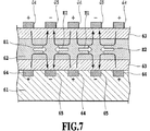
図6は、本実施形態に係る光スイッチの実施形態の他の一例であり、その位相変調部分の構成を示す図である。又、図7は、図6のVII−VII線矢視断面に該当し、櫛型電極を用いた位相変調部分の電界方向を示す図である。
【0053】
実施例3の光スイッチの構成は、実施例1の光スイッチと同様にマッハツェンダ干渉計を用いたものであるが、マッハツェンダ干渉計の光導波路(アーム導波路)の位相変調部分に、図6に示す櫛型の電極構造を用いたことが、大きく異なる点である。
【0054】
図6、図7に示すように、本実施例の位相変調部分は、基板61上に形成したクラッド63に、コア62が囲まれるように形成された埋め込み導波路となっている。コア62の上部には、その長さ方向に櫛型状の櫛型電極64とグランド電極65が、互いの電極が交互の配置になるように形成されている。又、図7に示すように(図6では図示せず)、上部側の櫛型電極64及びグランド電極65にそれぞれ対向するように、基板61とクラッド17の界面に、下部側の櫛型電極64及びグランド電極65がそれぞれ形成されている。
【0055】
櫛型電極64及びグランド電極65によって印加される電界は、図7に示す電界E1、E2のように、光の伝搬方向に平行な方向に複数形成される。そして、隣り合う電界E1、E2の方向が、交互に逆転する向きを持つ。対向する櫛型電極64、グランド電極65の極性が同相となるように電極が作製されている。従って、コア62に直交する方向の電界が打ち消され、コア62に平行する電界のみが残る。
【0056】
このような電界の印加前、印加後の光の伝搬方向に直交する屈折率を図示すると、図8のように変化することがわかる。実施例3の場合、光の伝搬方向に直交する方向の屈折率変化は、式(2)の屈折率変化に対応している。つまり、図8から明らかなように、この屈折率変化の方向は等方的であり、偏光に対して等方的に屈折率変化が生じる。よって、偏波無依存となることがわかる。
【0057】
実施例3の櫛型状の電極構造では、図7に示すように電界E1、E2の方向が交互に逆転しているにもかかわらず、電界の方向に依らず一定方向の屈折率変化が得られる特徴がある。これは、2次の電気光学効果を用いているため、電界の符号(電界の方向)に関係なく、その絶対値の2乗に比例する屈折率変化を得ることができるからである。これが、2次の電気光学効果を利用している大きな利点であり、櫛型電極を用いることを可能としている。
【0058】
更に、櫛型電極を用いる場合、櫛型電極のピッチを変えることで、電界の大きさを変えることができるという利点がある。サンドイッチ型の電極構造の場合、光導波路の厚み以下には電極間隔を小さくすることができず、電界を大きくするには大きい電圧を印加するしかない。しかしながら、櫛型電極の場合は正負の電極が同じ平面上にあり、その間隔を任意に変えることができる。よって、その間隔を小さくすることで、同じ印加電圧でありながら大きい電界を得ることができる。つまり、2次の電気光学効果を有する誘電体結晶に、櫛型電極を用いることで、小さい印加電圧でありながら大きい電界が印加できる。さらに、交互に電界の方向が変化しても一定方向に屈折率を変化させることができるため、屈折率が光の伝搬方向に一様に大きく変化した光導波路を得ることができる。したがって、実施例3の櫛型状の電極構造を用いた位相変調部分を、マッハツェンダ干渉計の一方(又は両方)のアーム導波路に用いることにより、偏波無依存かつ低駆動電圧の光スイッチを容易に実現することができる。
【0059】
なお、実施例3のような櫛型状の電極構造に限らず、光の伝搬方向に平行な方向であり、かつ、光の伝搬方向に順方向のみ又は逆方向のみの電界を形成するような電極構造の場合でも、偏波無依存の光スイッチを実現することができる。
【0060】
実施例3では、実施例1とほぼ等しい相転移温度を有するKTN結晶でマッハツェンダ干渉計を含む光導波路を作製した。また、下部電極に白金、上部電極にITOを用いて、光スイッチを作製した。電極は導電性のあるものであればスイッチング動作が可能である。上部及び下部のクラッド厚を薄くし、電界印加効率を上げた場合、透明電極を使用したほうが、電極材料による光吸収の影響を抑制することができる。その結果として挿入損失を低下させることができる。又、位相変調部分の長さを1cm、バイアス電圧を1Vとした場合、本実施例の光スイッチの駆動電圧Vπは0.98Vであり、消光比は35aBと良好な特性を示し、偏波無依存で動作する。
【0061】
なお、実施例1乃至実施例3の光スイッチにおいて、バイアス電圧を印加して動作させている。このバイアス電圧にスイッチングに必要な変調電圧を重畳することは、回路構成として容易である。又、2次の電気光学効果を用いているため、バイアス電圧を印加することで、電界変化に対する屈折率変化量を大きくすることが可能である。よって、電源回路に負荷をかけない程度のバイアス電圧を印加することで、さらに効率よいスイッチングが可能であることが明らかになった。
【0062】
(実施例4)
実施例4の光スイッチの構成は、実施例1の光スイッチと同様にマッハツェンダ干渉計を用いたものである。2本のアーム導波路をKLTN結晶により形成して、実施例1と同様の位相変調部分を両方のアーム導波路に作製した。但し、入力側3dBカップラ及び出力側3dBカップラは石英系導波路で作製されている。これらの材料を用いて、位相変調部分側のKLTN結晶の端面を研磨してARコートを施した上で、その端面を入力側3dBカップラ及び出力側3dBカップラと光学接着剤で接合して光スイッチを構成した。
【0063】
実施例4の光スイッチは、その駆動電圧やスイッチング速度は、実施例1とほぼ同様である。しかしながら、挿入損失ならびに消光比が改善され、それぞれ2.4dB、42dBとなる。これは、石英系導波路で作製された3dBカップラが、KLTN結晶で作製された3dBカップラより低損失で高精度であることを示している。このように、位相変調部分のみにKTN、KLTN結晶の光導波路を用い、その他の部分を石英系等の他の光導波路で構成しても、同様の光スイッチが作製できることが明らかになった。
【0064】
(実施例5)
実施例5の光スイッチは、実施例1の光スイッチと同等の構成であるが、光導波路がBTO結晶等で作製されている点が異なる。このような構成の光スイッチを作製し、その動作を確認した。
【0065】
実施例5の光スイッチにおいて、BTO導波路部分を110℃に制御して動作させると、駆動電圧Vπ、は1.5V必要である。しかしながら、実施例1の光スイッチと同様の性能が得られ、さらに、スイッチング速度は1ns以下である。また、BTOとSTOを0.73:0.27の割合で混合した、Ba0.73Sr0.27TiO3の単結晶からなる導波路を作製し、これを用いて同様な光スイッチを作製する。この場合、導波路温度10℃にて、BTOの導波路を用いた場合と同様な特性が得られる。その他、PLZTを導波路材料とした光スイッチでも同様な動作が可能であった。
【0066】
(実施例6)
実施例6では、実施例2の光スイッチを4インチの基板上に高密度に集積することで、16×16のマトリクススイッチを作製する。作製した光スイッチはノンブロッキング構成であり、その数は256個である。光スイッチは偏波無依存で動作し、挿入損は8.5dB、消光比は43dB、駆動電圧0.9V、スイッチングに使用した消費電力は0.8Wである。実施例6の光スイッチの場合、スイッチ部分の電気容量に対応する充放電をスイッチング時に繰り返すため、スイッチング速度に対応する電力消費が生じる。具体的には、1GHzで連続的にスイッチング動作が起きる場合、その最大の消費電力は0.8Wである。これにより、従来の光スイッチに比べ、極めて小さい電力消費であることが明らかになった。
【0067】
(実施例7)
本実施形態では、マッハツェンダ干渉型の光スイッチについて説明してきた。実施例7では、方向性結合器について説明する。
【0068】
図9に示すように、実施例7の導波路型デバイスではコア91、クラッド92に用いた導波路材料は共にKLTN結晶である。これら材料に対してLiの濃度とNbの濃度を調整することにより比屈折率差0.5%の光導波路を実現した。コアリッジはリソグラフィーとドライエッチングによりほぼ6μm×6μmのサイズに加工されている。
【0069】
実施例7は方向性結合型光分岐素子96を備えており、入力ポート93から光を入力すると相互作用領域において2つの導波路間にモード結合が生じ、エネルギーが移行する。コア間のギャップG及び相互作用領域Lを調節することにより1:1の分岐比を有する素子、すなわち3dBカップラを実現することができる。
【0070】
コアギャップG及び相互作用長Lを変化させた方向性結合型光分岐素子を複数作製した。入力ポート93から波長1.55μmの光を入力し出力ポート94,95からの出力光の強度を測定し、分岐比が1:1となる典型的な条件を示したグラフが図10である。図10より、作製した方向性結合型光分岐素子の過剰損失は概ね0.ldB以下と優れた光学特性を示した。
【0071】
(実施例8)
実施例7における方向性結合器において、一方の光導波路の直上に電極(図示せず)を形成し、分岐比可変導波路型分岐素子を作製した。その構造を図11に示す。
【0072】
実施例8の導波路型分岐素子では、図11に示すように入力ポート111から光を入力すると、位相変調部分112において、入力された光が一度もう一方の光導波路に移行した後、再び元の光導波路へ移行する。このとき、出力ポート114へすべての光が出力されるようバイアス電圧が印加されている。位相変調部分112において光導波路に分岐比制御用電界を印加する場合(ONの場合)は、位相変調部分112の電界の印加により片側導波路の実効屈折率が変化する。その結果、2つの導波路間の伝搬定数に差が生じ位相不整合が生じる。この位相不整合量を分岐比制御用電界で変化させることで、光の出力が出力ポート113へ移行し分岐比が変化することになる。
【0073】
図12は、図11における方向性結合器の一方の光導波路に形成した位相変調部分112を示す構成図である。また、図13Aは図12のXIIA−XIIA断面図であり、図13Bは図12のXIIB−XIIB断面図である。
【0074】
図12、図13AおよびBに示すように、位相変調部分112は、位相変調部121、位相変調部122の2つの位相変調部から構成されている。それぞれの位相変調部は、2種類の、各々異なる電極構造を有する。具体的には、位相変調部121ではコア91直上に電極123が配置されており、その両側にグランド電極124が配置されている。この電極構造では、図13Aに示すように、コア91から基板に向かう方向(伝搬する光のTM方向に平行な方向)に電界が印加される。一方、位相変調部122では、コア91をはさむように電極123、グランド電極124が配置されている。よって、図13Bに示すように、基板に平行な方向(伝搬する光のTE方向に平行な方向)に電界が印加される。このような電極構造により、光の伝搬方向に対して直交し、かつ、互いに直交する2方向に電界を印加することが可能である。
【0075】
すなわち、式(1)−(2)より、図11に示した位相変調部分112では、互いに直行する2つの電界が等しい場合には式(1)と(2)の加算分の屈折率変化がTE方向、TM方向の両変更に等しく生じる。そのため、位相変調部分112では、位相変調量は偏光に依存しないことになり本実施形態の光スイッチが偏光無依存で分岐比可変動作することがわかる。
【0076】
図12に示した2種類の電極の長さはそれぞれ4mmであり、両電極で約8mmとした。この光スイッチの挿入損失は約2.5dBであり、KLTN結晶を用いた方向性結合器を含む導波路デバイスが極めて低損失である。
【0077】
図14は、本実施形態に係る光スイッチの分岐特性を示すグラフである。上述のように位相変調部121,122に等しくバイアス電界(電圧)3Vを印加し、分岐比を変化させるために必要な電界を印加したときに、出力ポート113,114に出力される光パワーを測定した結果である。図14に示すように、光出力が電界の印加により切り替わることがわかる。実施例8の導波路型デバイスが分岐比可変であり、さらにスイッチング機能を有することがわかる。実施例8では、2次の電気光学効果を用いているため、印加電界が大きくなるに従い屈折率変化が大きくなる。このため、スイッチング動作に必要な電界が次第に小さくなっていく様子がわかる。本実施例の光スイッチの構成並びに駆動条件ではスイッチング動作に必要な電圧は0.95Vであり、スイッチの消光比は30dBと良好な値を示した。さらに、矩形波の電界をスイッチに印加して測定したスイッチング速度は約2nsecである。よって、本実施例の光スイッチにより、パケットスイッチングに必要となる高速動作も可能である。
【0078】
なお、実施例8では、KLTN結晶を用いたが、KTN結晶を用いても同様の光スイッチが作製でき、0.97Vの駆動電圧、1.7nsecのスイッチング速度、さらに、偏波無依存動作を確認した。また、位相変調を与えるための電極構成は図13AおよびBに示した2つの位相変調部からなる構成を用いたが櫛型電極等の構成を用いても偏波無依存操作を確認した。
【0079】
(実施例9)
実施例9では、実施例8の光スイッチを4インチの基板上に高密度に集積することで、16×16のマトリックススイッチを作製した。作製した光スイッチはノンプロッキング構造であり、その数は256個である。図15はその中で16個の要素151を示している。各要素151は図11に示した方向性結合器を用いた光スイッチである。この光スイッチは偏波無依存で動作し、挿入損失は8.0dB、消光比は45dB、駆動電圧0.90V、スイッチングに使用した消費電力は0.83Wであった。
【0080】
本スイッチの場合、スイッチ部分の電気容量に対応する充放電をスイッチング時に繰り返すため、スイッチング速度に対応する電力消費が生じる。具体的にはlGHzで連続的にスイッチング動作が起きる場合、その最大消費電力は0.8Wであり従来の光スイッチに比べ、きわめて小さい消費電力であった。
【0081】
第1の実施形態に係る光スイッチでは、KTNやKLTN等に対してキュリー転移温度近傍で動作させるために、温度コントローラを備えることができる。温度コントローラは、ペルチェ素子であっても良い。
【0082】
以上説明してきたように、第1の実施形態によれば、KTN、KLTN結晶等を光導波路として用いることにより、従来では実現できなかった高速、低電圧駆動、偏波無依存の光スイッチを実現することができる。低電圧で駆動できるため、高価な高速動作の電源を使用する必要がなく、替わりにIC等で直接駆動することができる。また、第1の実施形態に係る光スイッチは、集積回路やボード実装等を用いて、高密度のスイッチボードとして安価に作製することができる。更に、マトリクス構成することが容易であり、大規模なマトリクススイッチを構成することができる。よって、第1の実施形態に係る光スイッチは、光パケットルーターのコアスイッチとして有用である。
【0083】
(第2の実施形態)
第2の実施形態は、KTN結晶を基本とした光導波路を用いてデジタル光スイッチを構成する。例えば、図16に示すように、KTN若しくはKLTNをコア161とし、これより僅かに屈折率が低いKTN若しくはKLTNをクラッド層162とした埋め込み型三次元光導波路を用いる。図16中では、省略されているが、この埋め込み型三次導波路は、KTaO3(KT)、KNbO3(KN)若しくはKTN基板上に設けられている。
【0084】
このような埋め込み型三次元光導波路を利用した1×2デジタル光スイッチを図17に示す。この光スイッチは、光の導波路方向にのみ電界E1を印加するため、下層クラッドの下方かつ上層クラッドの上方に櫛形電極を具備する。
【0085】
即ち、基板173上には、コア178とクラッド層174とよりなる埋め込み型三次元光導波路として、一つの入力光導波路(入力ポート)175から二つの出力導波路(出力ポート)176,177へ分岐するY分岐型導波路を構成する。下側のクラッド層174の下方及び上側のクラッド層174の上方であって、Y分岐の近傍における出力導波路176,177には、コア178に電界を与えるために櫛形電極171,172を配置する。
【0086】
このようなデジタル光スイッチは、後述するように、TE,TM両方の屈折率変化が等しい屈折率変化を受けることが可能となり、偏光依存性が除去できる。本実施形態で用いるKTNは誘電体結晶材料であり、キュリー温度以上で立方晶構造を有する。これに対して、図16に示すように、外部電場E1,E2,E3を結晶軸方向a1,a2,a3に印加すると、二次の電気光学効果を示す。
【0087】
立方晶でのTE,TM各モードの屈折率の電場依存性は、E2若しくはE3が0の時には、以下のように記述できる。
【0088】
【数3】

上式において、n0はKTNまたはKLTNの電場印加前の屈折率であり、g11およびg12はKTN、KLTNの非線形定数であり、εaはKTN、KLTNの比誘電率である。ここで、E1,E2,E3の電界方向は、図16に示したコア108の主軸方向の電場に各々対応する。E2若しくはE3が0の時には、屈折率楕円体の主軸は変化せず、モード変換は起こらない。また、E3が0でない時には、g11とg12との符号が異なるため、屈折率変化の方向が異なる。
【0090】
そして、nTEはE3の増加に伴い減少する。一方、nTMはE3の増加に伴い増加するためスイッチ動作の偏波依存性を生じてしまう。そこで、光の導波方向の電界E1のみを印加すると、屈折率変化は両モードとも下式のように同一の式で与えられ、偏波依存性を除去できる。
【0091】
【数4】
そこで、図17のように、光の導波方向の電界E1のみを印加するために、コア178である出力ポート176、177の上下に櫛形電極171,172を配置した。
【0093】
櫛形電極171,172が配置されたY分岐導波路の断面図を図18Aに、櫛形電極の平面図を図18Bに示す。
【0094】
図18Aに示すように、基板183上にはクラッド層184とコア182とからなる埋め込み型三次元光導波路が設けられている。また、上側のクラッド層184の上方及び下側のクラッド層184の下側にはそれぞれ櫛型電極181が配置されている。図18Bに示すように、櫛型電極181は、+極181aと、−極181bとを一定間隔で交互に配置している。そして、上下の櫛型電極181の同極が向き合ように配置されている。
【0095】
そのため、コア182を上下に貫く電界E3は、上下の櫛型電極181からの電界成分の打ち消し合いにより理想的には0となる。よって、本実施例の櫛形電極181により、光の導波方向にのみ電界E1を効果的に印加することができる。更に、本発明の電界効果は、2次の電気光学効果を利用しているため電場の二乗に比例する。従って、二つの出力ポート176,177に予めDCバイアス電圧を印加しておいて、スイッチ動作により光路を切り替えたい二つの出力ポート176又は出力ポート177のみに電圧を印加することにより、より低消費電力でスイッチ動作できる。
【0096】
一方、図19に示すように、上側のクラッド層193の表面において、コア192の左右に+極、−極の電極191を配置し、光導波方向に対して垂直方向に電圧を印加した場合、基板に平行であってコア192を横切る方向の電界E2が主に発生する。その場合、屈折率変化は、以下の式で表せて、nTEは減少して、nTMは増加する。
【0097】
【数5】
このような原理を利用した1×2偏波スプリッタを図20に示す。即ち、図20に示すように、基板203上には、コア208とクラッド層204とよりなる埋め込み型三次元光導波路として、一つの入力ポート205から二つの出力ポート206,207へ分岐するY分岐型導波路を設けた。クラッド層204の表面には、Y分岐の近傍における出力ポート206,207のそれぞれ左右両側にスイッチング用電極201,202を配置した。
【0099】
従って、入力ポート205にTM光、TE光を入射させて、一方のスイッチング用電極201に電圧を印加すると、基板に平行であってコア208を横切る方向の電界E2が発生する。このため、TM光は出力ポート206へ、TE光は出力ポート207へ出力される。従って、TEモードとTMモードとを分離可能な偏波スプリッタが実現できる。
【0100】
また、図21AおよびBにこのY分岐型導波路を5個ツリー状に組み合わせた1×2偏波無依存光スイッチの模式図を示す。即ち、第一のY分岐型導波路211で一つの導波路を二つの導波路に分岐する。第二、第三のY分岐型導波路212,213で二つの導波路を四つに分岐する。第四、第五のY分岐型導波路214,215で交差した導波路と直線的な導波路をそれぞれ二つの導波路に結合させている。また、各Y分岐型導波路211〜215の出力導波路にはそれぞれスイッチング用電極が配置されている。図21AおよびB中に黒色で示す電極に実際に電圧が印加される。
【0101】
図21Aの場合、TM光、TE光は矢印で示した光路をそれぞれ伝播して、最終的には共に図中上側の出力ポートに出力される。一方、図21Bの場合、TM光、TE光は矢印で示した光路をそれぞれ伝播して、最終的には共に図中下側の出力ポートに出力される。
【0102】
また、図22AおよびBにこのY分岐型導波路を7個ツリー状に組み合わせた1×2偏波無依存光スイッチの模式図を示す。即ち、第一のY分岐型導波路221で一つの導波路を二つの導波路に分岐する。第二、第三のY分岐型導波路222,223で二つの導波路を更に四つの導波路に分岐する。第四のY分岐型導波路224で二つの導波路を一つの導波路に結合して第五のY分岐型導波路225で一つの導波路を二つの導波路に分岐する。更に、第六、第七のY分岐型導波路226,227で四つの導波路を二つの導波路に結合させている。これら各Y分岐型導波路221〜227の出力導波路にはそれぞれスイッチング用電極が配置されている。図22AおよびB中に黒色で示す電極に実際に電圧が印加される。
【0103】
図22Aの場合、TM光、TE光はそれぞれ矢印で示した光路を伝播して、最終的には共に図中上側の出力ポートに出力される。一方、図22Bの場合、TM光、TE光は矢印で示した光路を伝播して、最終的には共に下側の出力ポートに出力される。
【0104】
以上のように、多段にY分岐型導波路を連結することにより偏波無依存型の光スイッチが実現できる。図21AおよびB、ならびに図22AおよびBのように、Y分岐型導波路を5〜7個のツリー状に連結することで最小の小型の偏波無依存型のスイッチを実現できる。
【0105】
一方、図23のように下側のクラッド層233の下方かつ上側のクラッド層233の上方の両方に+電極231及び−電極231を配置する。光導波方向に対して垂直方向に電圧を印加した場合、基板に垂直であってコア導波路232を横切る方向の電界E3が主に発生する。
【0106】
【数6】
この場合、電圧印加時には、nTEは増加して、nTMは減少する。
【0108】
このような原理を利用した1×2偏波スプリッタを図24に示す。図24に示すように、基板248上には、コア241とクラッド層244とよりなる埋め込み型三次元光導波路として、一つの入力ポート245から二つの出力ポート246,247へ分岐するY分岐型導波路を設けた。クラッド層244の上面及びその下面には、Y分岐の近傍における出力ポート246,247のそれぞれに沿ってスイッチング用電極242,243を配置した。
【0109】
このような構成で、入力ポート245にTM光、TE光を入射させて、一方のスイッチング用電極242に電圧を印加すると、基板に垂直であってコア246を横切る方向の電界E3を発生させる。よって、TE光は出力ポート246へ、TM光は出力ポート247へ出力される。従って、同様にTEモードとTMモードとを分離可能な偏波スプリッタが実現できる。
【0110】
また、図25AおよびBにこのY分岐型導波路を5個ツリー状に組み合わせた1×2偏波無依存光スイッチの模式図を示す。即ち、第一のY分岐型導波路251で一つの導波路を二つの導波路に分岐する。第二、第三のY分岐型導波路252,253で二つの導波路を四つに分岐する。第四、第五のY分岐型導波路254,255で交差した導波路と直線的な導波路をそれぞれ二つの導波路に結合させている。これら各Y分岐型導波路251〜255の出力ポートにはそれぞれスイッチング用電極が配置されている。図25A、B中に黒色で示す電極に実際に電圧が印加される。
【0111】
図25Aの場合、TM光、TE光は矢印で示した光路をそれぞれ伝播して、最終的には共に図中上側の出力ポートに出力される。一方、図25Bの場合、TM光、TE光は矢印で示した光路をそれぞれ伝播して、最終的には共に図中下側の出力ポートに出力される。
【0112】
また、図26AおよびBにこのY分岐型導波路を7つ組み合わせた1×2偏波無依存光スイッチの模式図を示す。即ち、第一のY分岐型導波路261で一つの導波路を二つの導波路に分岐する。第二、第三のY分岐型導波路262,263で二つの導波路を更に四つの導波路に分岐する。第四のY分岐型導波路264で二つの導波路を一つの導波路に結合して第五のY分岐型導波路265で一つの導波路を二つの導波路に分岐する。更に第六、第七のY分岐型導波路266,267で四つの導波路を二つの導波路に結合させている。
【0113】
各Y分岐型導波路261〜267の出力ポートにはそれぞれスイッチング用電極が配置されている。図26AおよびB中に黒色で示す電極に実際に電圧が印加される。
【0114】
図26Aの場合、TM光、TE光は矢印で示した光路をそれぞれ伝播して、最終的には共に図中上側の出力ポートに出力される。一方、図26Bの場合、TM光、TE光は矢印で示した光路をそれぞれ伝播して、最終的には共に図中下側の出力ポートに出力される。以上のように、多段にY分岐型導波路を連結することにより偏波無依存型の光スイッチが実現できる。
【0115】
以下に、上記の手法により作製した光スイッチの実施例を示すが、スイッチ作製手法は記述の内容に限定されるものではない。
【0116】
(実施例1)
フォトリソグラフィーなどの手法により、KTN結晶の表面に白金櫛形電極を作製した。そしてその上に、Li濃度を調整して屈折率の高いKLTNをY分岐型のコアとし屈折率の低いKLTNをクラッド層としたY分岐埋め込み導波路を作製する。そこで、コアとクラッドとの比屈折率差はΔn=0.3%とした。コアサイズは、8×8μm2とする。更に、フォトリソグラフィーなどの手法により、上層クラッド結晶の表面に白金櫛形電極を作製して駆動用電極とする。
【0117】
電極長は、短いほどCR定数で決定される応答速度に有利である。しかしながら、クロストークは電極長が長いほど有利である。よって、電極長を変えたパタンを有する複数の光スイッチでその光学特性を評価し、最適値を得た。キュリー転移温度近傍で動作させるため、この光スイッチをペルチェ素子で温度調整する。DCバイアス3Vを双方のスイッチング用電極に印加し、ONポート側のスイッチング用電極に変調電圧を印加し、スイッチ動作させる。この1×2デジタル型EOスイッチは、動作電圧<1V(DCバイアス3V)、クロストーク<−30dB、応答速度<1nsの光学特性を示した。
【0118】
(実施例2)
フォトリソグラフィーなどの手法により、KTN結晶の表面に白金の櫛形電極を作製する。そしてその上に、Ta/Nb濃度比を調整して屈折率の高いKTNをコアとし屈折率の低いKTNをクラッド層としたY分岐埋め込み導波路を作製する。コアとクラッドとの比屈折率差はΔn=0.3%とした。コアサイズは、8×8μm2とする。更に、フォトリソグラフィーなどの手法により、上層クラッド結晶の表面に白金櫛形電極を作製して駆動用電極とする。
【0119】
電極長は、短いほどCR定数で法定される応答速度に有利である。しかしながら、クロストークは電極長が長いほど有利である。よって、クロストークは電極長が長いほど有利であるため、電極長を変えたパタンを有する複数の光スイッチでその光学特性を評価し、最適値を得た。キュリー転移温度近傍で動作させるために、この光スイッチをペルチェ素子で温度調整する。DCバイアス3Vを双方のスイッチング用電極に印加し、一方のスイッチング用電極に変調電圧を印加し、スイッチ動作させる。この1×2デジタル型EOスイッチは、動作電圧<1V(DCバイアス3V)、ク回ストーク<−30dB、応答速度<1nsの光学特性を示した。
【0120】
(実施例3)
Ta/Nb濃度比を調整して屈折率の高いKTNをコアとし屈折率の低いKTNをクラッド層とした導波路を作製する。この導波路を用いて、図22AおよびBに示したようにY分岐型導波路221〜227を7段に連結した構造の埋め込み導波路を作製する。コアとクラッドとの比屈折率差はΔ=0.3%とした。コアサイズは、8×8μm2とする。更に、フォトリソグラフィーなどの手法により、上層クラッド結晶の表面に白金表面電極を作製してスイッチング用電極とする。キュリー転移温度近傍で動作させるために、この光スイッチをペルチェ素子で温度調整する。
【0121】
図22AおよびBの黒色で示す電極に変調電圧を印加し、スイッチ動作させる。この1×2デジタル型EOスイッチは、動作電圧<1V(DCバイアス3V)、クロストーク<−30dB、応答速度<1nsの光学特性を示した。
【0122】
(実施例4)
Ta/Nb濃度比を調整して屈折率の高いKTNをコアとし屈折率の低いKTNをクラッド層とした導波路を作製する。この導波路を用いて、図21AおよびBに示したようにY分岐型導波路211〜215を5段に連結した構造の埋め込み導波路を作製する。コアとクラッドとの比屈折率蓬はΔn=0.3%とした。コアサイズは、8×8μm2とする。更に、フォトリソグラフィーなどの手法により、上層クラッド結晶の表面に白金表面電極を作製して駆動用電極とする。キュリー転移温度近傍で動作させるために、この光スイッチをペルチェ素子で温度調整する。
【0123】
図21AおよびBの黒色で示す電極に変調電圧を印加しスイッチ動作させる。この1×2デジタル型EOスイッチは、動作電圧<1V(DCバイアス3V)、クロストーク<−30dB、応答速度<1nsの光学特性を示した。
【0124】
(実施例5)
フォトリソグラフィーなどの手法により、KTN結晶の表面に白金のスイッチ用電極を作製する。そしてその上に、Ta/Nb濃度比を調整して屈折率の高いKTNをコアとし屈折率の低いKTNをクラッド層とした導波路を作製する。その導波路を用いて、図25AおよびBに示したようにY分岐型導波路251〜255を5段に連結した構造の埋め込み導波路を作製する。そこで、コアとクラッドとの比屈折率差はΔn=0.3%とした。コアサイズは、8×8μm2とする。更に、フォトリソグラフィーなどの手法により、上層クラッド結晶の表面及び下層クラッド結晶下部に白金電極を作製してスイッチング用電極とする。キュリー転移温度近傍で動作させるために、この光スイッチをペルチェ素子で温度調整する。
【0125】
図25AおよびBの黒色で示す電極に変調電圧を印加し、スイッチ動作させる。この1×2デジタル型EOスイッチは、動作電圧<1V(DCバイアス3V)、クロストーク<−30dB、応答速度<1nsの光学特性を示した。
【0126】
(実施例6)
フォトリソグラフィーなどの手法により、KTN結晶の表面に白金のスイッチ用電極を作製する。そしてその上に、Ta/Nb濃度比を調整して屈折率の高いKTNをコアとし屈折率の低いKTNをクラッド層とした導波路を作製する。この導波路を用いて、図26AおよびBに示したようなY分岐型導波路261〜267が7段に連結した構造の埋め込み導波路を作製する。そこで、コアとクラッドとの比屈折率差はΔn=0.3%とした。コアサイズは、8×8μm2とする。更に、フォトリソグラフィーなどの手法により、上層クラッド結晶の表面及び下層クラッド結晶下部に白金電極を作製して駆動用電極とする。キュリー転移温度近傍で動作させるために、この光スイッチをペルチェ素子で温度調整する。
【0127】
図26AおよびBの黒色で示す電極に変調電圧を印加し、スイッチ動作させる。この1×2デジタル型EOスイッチは、動作電圧<1V(DCバイアス3V)、クロストーク<−30dB、応答速度<1nsの光学粋性を示した。
【0128】
(実施例7)
実施例7の光スイッチは、実施例1の光スイッチと同等の構成であるが、光導波路がBTO結晶等で作製されている点が異なる。このような構成の光スイッチを作製し、その動作を確認した。
【0129】
実施例7の光スイッチにおいて、BTO導波路部分を110℃に制御して動作させると、動作電圧は1.5V必要である。しかしながら、実施例1の光スイッチと同様の性能が得られ、さらに、スイッチング速度は1ns以下である。また、BTOとSTOを0.73:0.27の割合で混合した、Ba0.73Sr0.27TiO3の単結晶からなる導波路を作製し、これを用いて同様な光スイッチを作製する。この場合、導波路温度10℃にて、BTOの導波路を用いた場合と同様な特性が得られる。その他、PLZTを導波路材料とした光スイッチでも同様な動作が可能であった。
【0130】
第2の実施形態に係る光スイッチでは、KTNやKLTN等に対してキュリー転移温度近傍で動作させるために、温度コントローラを備えることができる。温度コントローラは、ペルチェ素子であっても良い。
【0131】
以上説明したように、本実施形態は、誘電体結晶基板と誘電体結晶導波路とを用いた光デバイスに関し、具体的には、KTaO3若しくはKNbO3若しくはKTN基板と、この基板上にKLTNをコアとし、コアより僅かに屈折率が低いKLTN導波路をクラッド層とした埋め込み型光導波路と、電界を与える電極とを具備した光デバイスである。
【0132】
以上説明したように、第2の実施形態によれば、偏波無依存動作可能な光スイッチなどの導波路型デバイスを実現できる。つまり、第の実施形態では、KTN/KLTN結晶材料を用いた埋め込み型導波路にスイッチング用電極を具備するので、小型で安価な高速電源を用いてスイッチ動作が可能という効果がある。
【0133】
更に、偏波無依存、集積化できるためネットワークシステム用の高速スイッチ、例えば、光パケットスイッチとして用いることができ、新規なネットワークシステムを提供できるという効果がある。
【0134】
(第3の実施形態)
第3の実施形態は、電気光学定数が極めて大きい立方晶かつ2次の電気光学定数を有する誘電体結晶を基本とした位相シフタを用いて構成した光変調器を特徴とするものである。本実施形態では、上述の誘電体結晶として、KTN、KLTNを用いている。
【0135】
立方晶でのTE,TM各モードの屈折率の電場依存性は、E2もしくはE3が0の時には、以下のように記述できる。つまり、TE,TM各モードの屈折率の電場依存性は、E2もしくはE3が0の時には、以下のように記述できる。
【0136】
【数7】
【数8】
上式において、n0はKTNまたはKLTNの電場印加前の屈折率であり、g11およびg12はKTN、KLTNの非線形定数であり、εaはKTN、KLTNの比誘電率である。また、g11=0.136であり、g12=−0.038である。
【0139】
図27は、誘電体結晶材料の導波路の結晶方位と電界方向を示す立体図で、図中符号271はコア、符号272はクラッドを示している。ここで、E1,E2,E3の電界方向は、KTN導波路の主軸方向の電場に各々対応する。E2もしくはE3が0の時には、屈折率楕円形の主軸は変化せず、モード変換はおこらない。
【0140】
図28A,Bは、櫛形電極付光導波路の構成図である。図28Aは、櫛形電極付光導波路の斜視図であり、図28Bは図28AのXXVIIIB−XXVIIIB線切断断面図である。図中符号281はコア、符号282はクラッド、符号283は基板、符号284は櫛型電極を示している。コア281の上下を挟むようにして櫛型電極284が配置される。この櫛型電極284は、長手方向に正極及び負極が交互に配置されている。つまり、基板283上には、クラッド282が形成され、このクラッド282中にはコア281が埋め込まれている。クラッド282の上下には櫛形状電極284が配設されている。
【0141】
図28AおよびBに示すように、電極284によりE1のみに電界をかけると、屈折率変化は両モードとも下記の式のように同一の式で与えられる。よって、偏波依存性を除去できる。
【0142】
【数9】
【数10】
図29AおよびBは、電極付光導波路の構成図である。図29Aは電極付導波路の斜視図であり、図29Bは図29AのXXIXB−XXIXB線切断断面図である。図中符号291はコア、292はクラッド、293は基板、294は電極を示している。この電極294は、コア291の上方でクラッド292面上にその直上及びその両側に3つ配置されている。
【0145】
図29AおよびBに示すように、電極294によりE2のみに電界をかけると、屈折率変化は下式のように与えられる。
【0146】
【数11】
【数12】
図30AおよびBは、電極付光導波路の構成図である。図30Aは電極付導波路の斜視図であり、図30Bは図30AのXXXB−XXXB線切断断面図である。図中符号301はコア、302はクラッド、303は基板、304は電極を示している。この電極304は、コア301の上方でクラッド302面上にその直上の両側に2つ配置されている。
【0149】
図30AおよびBに示すように、電極304によりE3のみに電界をかけると、屈折率変化は下式のように与えられる。
【0150】
【数13】
【数14】
後者の2つの電界印加配置では、屈折率の変化が両モードにおいて逆符号となる。図31(実施例15で詳説する)には、マッハ・ツェンダ型の光変調器の基本構造が示されている。入力光は3dBカップラ312によって2分され、Y分岐光導波路314に導かれる。このY分岐光導波路314の一方は光位相変調器として動作し、そこを通過する光の位相を変調する。
【0153】
Y分岐光導波路314からの光波が同位相で入射した場合は、2つの光波はそのまま足しあわされて出力ポートに導かれる。しかしながら、両者の位相が180度ずれている場合には、光は放射モードとしてY分岐光導波路314から外へ放射されるために出力ポート316へは導かれない。KTNは大きな2次の電気光学効果を有するために、電流長を短くしても式(7)または(8)、あるいは(11)乃至式(14)から導かれる屈折率変化に応じた位相の変化により効率よく光強度変調を実現できる。
【0154】
図31に示した電極構造を用いると偏波無依存動作を実現できるが、図32(実施例16で詳説する)及び図33(実施例17で詳説する)に応じた電極を用いると偏波依存動作になる。しかしながら、図32および図33に応じた電極を用いると、より大きな非線形定数(g11)を用いることが可能で、より低電圧での強度変調が可能になる。通常、強度変調する光源としては、偏光したレーザ光を変調する場合が多い。よって、偏光依存動作でもレーザ偏光に応じた光を変調することが可能であれば実用上は問題にならないと考えられる。
【0155】
さらに、図34(実施例18で詳説する)に示すように、一方のY分岐光導波路344に図29AおよびBの電極を、他方のY分岐光導波路344に図30AおよびBの電極を用いた場合、非線形定数が逆符号のため位相変調の方向を互いに逆相にしたプッシュープル動作によって変調能率を増加することも可能である。
【0156】
ところで、相転移近傍のKTNの誘電率は、他材料に比べて非常に大きい。このため、電気容量を小さくするための工夫が必要である。表面電極を用いる場合、デバイスの電気容量は、電極間ギャップが小さく、かつ光導波路層の厚みが大きいほど大きくなると考えられる。電極間ギャップは狭いほど、強電界をコアに印加することが可能である。よって、電極間ギャップは、可能な限り狭いほうが望ましい。そこで、コア厚をhcとしたとき、下層クラッド厚hu及び上層クラッド厚hoが、0≦hu,ho≦3hcの範囲にある埋め込み導波路は、1GHz以上の高速動作のため十分低い電気容量であることが確かめられた。
【0157】
しかしながら、クラッド層が1μm以下の薄層になると、単純な金属電極を用いた場合、TMモードの導波路光は、メタルクラディングの影響により、100dB/cm以上におよぶ大きな損失を生じる。そこで、通信波長帯で高い透明性を有するITO及びZnOを電極材料に用いて、低損失な位相シフタを実現する。また、1μmを超えるクラッド厚の場合、単純な金属、例えば、Pt,Au,Pd,Ti,Cuに代表される金属やこれらの合金を電極材料として用いることも可能である。
【0158】
また、コアとクラッドの比屈折率差を大きくすることによって、コア層の厚さを薄層化することにより、電気容量を小さくすることも可能である。例えば、屈折率差を1.5%にすれば、シングルモード導波のためのコア厚は、4μmまで小さくすることができる。屈折率差の大きいコア及びクラッドを用いることにより、低い電気容量を有するデバイスを実現することが可能となった。基板に用いられる結晶材料として、導波路を構成する結晶材料の比誘電率よりも一桁以上低い比誘電率をもつものとすると、なお一層電気容量の低下に対して効果がある。以上に示した、低電圧駆動位相シフタを用いると、高い変調指数を有する光強度変調器を広帯域で実現することが可能となる。
【0159】
さらに、より効果的な駆動電圧の低減法として、コア上のクラッド厚が重要なパラメータであることを確かめた。クラッド厚が小さいほど、駆動電圧を低減できる。そこで、コア幅をWとしたとき、コア上のクラッドの厚さh及び電極のギャップgが、0≦h≦3W、0≦g≦3Wの範囲にあれば、1GHz以上の高速動作のため十分低い駆動電圧であることを確認している。しかし、クラッド厚が1μm以下の薄層になると、単純な金属電極を用いた場合、TMモードの導波路光はメタルクラディングの影響により100dB/cm以上におよぶ大きな損失を生じる。そこで、通信波長帯で高い透明性を有するITOおよびZnOを電極材料に用いて、低損失な位相シフタを実現する。
【0160】
さらに、KTN材料は2次の電気光学効果を示すため、バイアス電圧を印加すれば駆動電圧を低減できる。一般に、駆動電圧は位相シフタ中の導波路の位相がπ変化するVπで定義される。Vπとバイアス電圧Vb印加時の駆動電圧Vmは以下の関係がある。
【0161】
【数15】
上式に従って、駆動電圧を低減することが可能である。例えば、無バイアス時のVπが2.5Vの位相シフタにおいて、6Vのバイアスを印加すると駆動電圧は0.5Vにまで低減する。
【0163】
また、1μmを超えるクラッド厚の場合は、単純な金属例えば、Pt,Au,Pd,Ti,Cuに代表される金属やこれらの合金を電極用材料として用いることも可能である。以上に示した低電圧駆動位相シフタを用いると、高い変調指数を有する光強度変調器を実現することが可能となる。
【0164】
以下に実施例を示すが、本発明はこれらの実施例に限定されるものではない。
以下、図面を参照して本発明の実施例について説明する。
(実施例1)
実施例1は、図30AおよびBの電極を用いた場合の導波路電気光学位相シフタの実施例である。
【0165】
本実施形態の導波路電気光学位相シフタは、立方晶で2次の電気光学効果を有する結晶を用いている。コア幅wを有するコア301上のオーバー(上層)クラッド厚hが、0≦h≦3wの範囲の厚みを有する埋め込み型のチャネル光導波路を備えた導波路電気光学位相シフタである。チャネル光導波路を挟んで平行に対向する2つの電界印加用薄膜電極(単に電極とも呼ぶ)304が配置されている。
【0166】
また、電極間のギャップgは、0≦g≦3wの範囲の長さを有している。また、結晶として、KTN及びKLTNからなる組成の結晶材料を用いている。さらに、電極として、Al,Ga,InおよびBの中の少なくとも1つがドーピングされたZnOもしくはSn,Ti,Zr,Hf,Nb,Ra,W,Ge,Mo,Sb,Te,Au,PtおよびPgの中の少なくとも1つがドーピングされたITOを電極材料として用いている。
【0167】
以下、実施例1の導波路電気光学位相シフタの作製方法について説明する。
【0168】
まず、Ta/Nb濃度比を調整して、屈折率2.184を有するKTNをコアとし、屈折率の低いKTNをクラッドとした埋め込み型光導波路を作製する。また、さらに精密な屈折率の調整法としては、Liをクラッド、コア各層にドープして制御する。光導波路のコア断面サイズは6μm×6μmとする。コア上のクラッド厚を0μmに設定する。
【0169】
さらに、光導波路上にITO膜をスパッター法で形成し、フォトリソグラフィーおよびドライエッチング法を用いてギャップ幅6μm、電極幅100μm、厚さ1μm、ギャップ幅6μmのSnドープされたITOからなる電界印加用電極を作製する。電極長は1mmとする。印加電圧の反射を抑えるために、電極を50オームに終端した。波長1.55μmのレーザ光源を入力ポートに接続してオシロスコープを用いて変調特性を測定した。駆動時には、デバイス温度を相転移近傍にコントロールした。変調動作電圧は、無バイアス時、2.5V以下であった。また、6Vのバイアス電圧印加時には、変調動作電圧は0.5V以下であった。
【0170】
(実施例2)
本実施例2は、図29AおよびBの電極を用いた場合の導波路電気光学位相シフタの実施例である。以下、実施例2の導波路電気光学位相シフタの作製方法について説明する。
【0171】
まず、Ta/Nb濃度比を調整して、屈折率2.184を有するKTNをコアとし、屈折率の低いKTNをクラッドとした埋め込み型光導波路を作製する。また、さらに精密な屈折率の調整法としては、Liをクラッド、コア各層にドープして制御する。光導波路のコア断面サイズは6μm×6μmとする。コア上のクラッド厚を0μmに設定する。
【0172】
さらに、光導波路上にITO膜をスパッター法で形成し、フォトリソグラフィーおよびドライエッチング法を用いてギャップ幅6μm、電極幅100μm、厚さ1μm、ギャップ幅6μmのAlドープされたITOからなる電界印加用電極を作製する。電極長は1mmとする。印加電圧の反射を抑えるために、電極を50オームに終端した。波長1.55μmのレーザ光源を入力ポートに接続してオシロスコープを用いて変調特性を測定した。駆動時には、デバイス温度を相転移近傍にコントロールした。変調動作電圧は、無バイアス時、2.5V以下であった。また、6Vのバイアス電圧印加時には、変調動作電圧は0.5V以下であった。
【0173】
(実施例3)
本実施例3は、単純な金属を電極材料に用いて、図30AおよびBの電極を用いた場合の導波路電気光学位相シフタの実施例である。Ta/Nb濃度比を調整して、屈折率2.184を有するKTNをコアとし、屈折率の低いKTNをクラッドとした埋め込み型光導波路を作製する。また、さらに精密な屈折率の調整法としては、Liをクラッド、コア各層にドープして制御する。光導波路のコア断面サイズは6μm×6μmとする。コア上のクラッド厚を6μmに設定する。
【0174】
さらに、光導波路上に金薄膜をスパッター法で形成し、フォトリソグラフィーおよびドライエッチング法を用いてギャップ幅6μm、電極幅100μm、厚さ1μm、ギャップ幅6μmのAuからなる電界印加用電極を作製する。電極長は3mmとする。印加電圧の反射を抑えるために、電極を50オームに終端した。駆動時には、デバイス温度を相転移近傍にコントロールした。波長1.55μmのレーザ光源を入力ポートに接続してオシロスコープを用いて変調特性を測定した。変調動作電圧は、無バイアス時、6V以下であった。
【0175】
(実施例4)
本実施例4は、単純な金属を電極材料に用いて、図29AおよびBの電極を用いた場合の導波路電気光学位相シフタの実施例である。Ta/Nb濃度比を調整して、屈折率2.184を有するKTNをコア部とし、屈折率の低いKTNをクラッド部とした埋め込み型光導波路を作製する。また、さらに精密な屈折率の調整法としては、Liをクラッド、コア各層にドープして制御する。光導波路のコア断面サイズは6μm×6μmとする。コア上のクラッド厚を6μmに設定する。
【0176】
さらに、光導波路上に金薄膜をスパッター法で形成し、フォトリソグラフィーおよびドライエッチング法を用いてギャップ幅6μm、電極幅100μm、厚さ1μm、ギャップ幅6μmのPtからなる電界印加用電極を作製する。電極長は3mmとする。印加電圧の反射を抑えるために、電極を50オームに終端した。駆動時には、デバイス温度を相転移近傍にコントロールした。波長1.55μmのレーザ光源を入力ポートに接続してオシロスコープを用いて変調特性を測定した。TE,TM両モードとも、変調指数が直流値の1/2に低下する帯域幅は5GHzで、変調動作電圧は、無バイアス時、6V以下であった。抵抗に終端抵抗を用いて50オームに調整した。波長1.55μmのレーザ光源を入力ポートに接続してオシロスコープを用いて変調特性を測定した。変調動作電圧は6V以下であった。
【0177】
(実施例5)
図34は、図29AおよびB並びに図30AおよびBに示した電極を導波路電気光学位相シフタとして用いた場合の本実施形態に係るマッハ・ツェンダ光強度変調器の実施例を示す構成図である。図中符号340はクラッド、符号341は入力ポート、符号342は3dBカップラ、符号343a、bおよびcは電極(電界印加部)、符号344はY分岐光導波路(三次元光導波路)、符号345は3dBカップラ、符号346は出力ポート、符号347は印加用電源を示している。このマッハ・ツェンダ光強度変調器は、1個の入力ポート341と、この入力ポート341に連結された3dBカップラ342と、この3dBカップラ342に連結された三次元光導波路344と、この三次元光導波路344に連結された3dBカップラ345と、この3dBカップラ345に連結された出力導波路346とを供えている。また、手前のチャネル導波路には図30AおよびBに示す電極を配置し、奥のチャネル導波路には図29AおよびBに示す電極を配置した構成である。
【0178】
このような構成にすれば、図29AおよびBと図30AおよびBとに示した電極を有する位相シフタのTEモードとTMモードとに対する位相シフタが相補的になる。よって、この構成の光強度変調器は、偏波無依存動作が可能になる。実際、TE、TM両モードとも、変調指数が直流値の1/2に低下する帯域幅は5GHzであり、無バイアス時の変調動作電圧は2.5V以下であった。
【0179】
しかしながら、偏波が固定されているのであれば、入射光がTEモードであるかTMモードであるかに応じて、2つのチャネル導波路の何れか一方に図29AおよびBあるいは図30AおよびBに示した電極を配置すれば、同様の効果を奏することは言うまでもない。
【0180】
(実施例6)
図35AおよびBは、本発明に係る電極を用いた場合の導波路電気光学位相シフタの実施例6を説明するための構成図である。図35Aは導波路電気光学位相シフタを説明するための斜視図であり、図35Bは図39AのXXXVB−XXXVB線断面図である。図中符号350はコア、符号351はクラッド、符号352は基板、符号353は電極を示している。
【0181】
本実施形態の導波路電気光学位相シフタは、立方晶で2次の電気光学効果を有する結晶を用いている。その結晶のコア厚をhcとしたとき、下層クラッド厚hu及び上層クラッド厚hoが、0≦hu,ho≦3hcの範囲の厚みを有する埋め込み型の三次元光導波路を備えた導波路電気光学位相シフタである。その位相シフタには、三次元光導波路を挟んで平行に対向する2つの電極353が配置されている。
【0182】
また、結晶として、KTNおよびKLTNからなる組成の結晶材料を用いた基板上に、KTNおよびKLTNからなる組成の結晶材料を導波路として用いている。
【0183】
また、結晶材料の組成比として、組成比Xを0以上かつ1以下とし、組成比Yを0より大きく0.1未満としている。また、導波路の材料としてKTNおよびKLTNの比誘電率が、基板に用いられている結晶材料の比誘電率よりも一桁以上大きいようになっている。
【0184】
さらに、コアとクラッドの比屈折率差が、0%より大きく1.5%以下である。また、電極として、Al,Ga,InおよびBの中の少なくとも1つがドーピングされたZnOもしくはSn,Ti,Zr,Hf,Nb,Ra,W,Ge,Mo,Sb,Te,Au,PtおよびPgの中の少なくとも1つがドーピングされたITOを用いている。
【0185】
以下、実施例6の導波路電気光学位相シフタの作製方法について説明する。
まず、Ta/Nb濃度比を調整して、屈折率2.184を有するKTNをコア部とし、屈折率の低いKTNをクラッド部とした埋め込み型光導波路を作製する。導波層の比誘電率は、基板352のそれよりも一桁以上大きいことが確かめられる。さらに精密な屈折率の調整法としては、Liをクラッド、コア各層にドープして制御する。コア350とクラッド351との屈折率差は0.5%として、光導波路のコア断面サイズは6μm×6μmとする。コア350下の下層クラッド厚huを6μm、コア350上の上層クラッド厚hoを1μmに設定する。
【0186】
さらに、光導波路上に金薄膜をスパッター法で形成し、フォトリソグラフィーおよびドライエッチング法を用いてギャップ幅6μm、電極幅100μm、厚さ1μm、ギャップ幅6μmのSnドープされたITOからなる電界印加用電極を作製する。電極長は1mmとする。印加電圧の反射を抑えるために、電極を50オームに終端した。波長1.55μmのレーザ光源を入力ポートに接続してオシロスコープを用いて変調特性を測定した。駆動時には、デバイス温度を相転移近傍にコントロールした。変調動作電圧は、無バイアス時、2.5V以下であった。また、6Vのバイアス電圧印加時には、変調動作電圧は0.5V以下であった。また、10GHz程度まで応答特性は劣化しないことを確かめた。
【0187】
(実施例7)
図36AおよびBは、本実施形態に係る電極を用いた場合の導波路電気光学位相シフタの実施例7を説明するための構成図である。図36Aは導波路電気光学シフタを説明するための斜視図であり、図36Bは図36AのXXXVIB−XXXVIB線断面図である。図中符号360はコア、符号361はクラッド、符号362は基板、符号363は電極を示している。この実施例7の位相シフタは、三次元光導波路を挟んで平行に対向する2つの電極363が配置されているとともに、チャネル導波路上に1つの電極363が配置されている。
【0188】
以下、実施例7の導波路電気光学位相シフタの作製方法について説明する。
まず、Ta/Nb濃度比を調整して、屈折率2.184を有するKTNをコアとし、屈折率の低いKTNをクラッドとした埋め込み型光導波路を作製する。導波層の比誘電率は、基板362のそれよりも一桁以上大きいことが確かめられる。また、さらに精密な屈折率の調整法としては、Liをクラッド、コア各層にドープして制御する。コア360とクラッド361の屈折率差は0.5%として、光導波路のコア断面サイズは6μm×6μmとする。コア360下の下層クラッド厚huを6μm、コア360上の上層クラッド厚hoを1μmに設定する。
【0189】
さらに、光導波路上にITO膜をスパッター法で形成し、フォトリソグラフィーおよびドライエッチング法を用いてギャップ幅6μm、電極幅100μm、厚さ1μm、ギャップ幅6μmのSnドープされたITOからなる電界印加用電極を作製する。電極長は1mmとする。印加電圧の反射を抑えるために、電極を50オームに終端した。波長1.55μmのレーザ光源を入力ポートに接続してオシロスコープを用いて変調特性を測定した。駆動時には、デバイス温度を相転移近傍にコントロールした。変調動作電圧は、無バイアス時、2.5V以下であった。また、6Vのバイアス電圧印加時には、変調動作電圧は0.5V以下であった。また、10GHz程度まで応答特性は劣化しないことを確かめた。
【0190】
(実施例8)
本実施例8は、単純な金属を電極材料に用いて、図35AおよびBの電極を用いた場合の導波路電気光学位相シフタの実施例である。
【0191】
以下、実施例8の導波路電気光学位相シフタの作製方法について説明する。
まず、Ta/Nb濃度比を調整して、屈折率2.184を有するKTNをコアとし、屈折率の低いKTNをクラッドとした埋め込み型光導波路を作製する。さらに精密な屈折率の調整法としては、Liをクラッド、コア各層にドープして制御する。コア350とクラッド351の屈折率差は0.5%として、光導波路のコア断面サイズは6μm×6μmとする。コア350下の下層クラッド厚huを1μm、コア350上の上層クラッド厚hoを6μmに設定する。
【0192】
さらに、光導波路上に金薄膜をスパッター法で形成し、フォトリソグラフィーおよびドライエッチング法を用いてギャップ幅6μm、電極幅100μm、厚さ1μm、ギャップ幅6μmのAuからなる電界印加用電極を作製する。電極長は3mmとした。印加電圧の反射を抑えるために、電極を50オームに終端した。駆動時には、デバイス温度を相転移近傍にコントロールした。波長1.55μmのレーザ光源を入力ポートに接続してオシロスコープを用いて変調特性を測定した。変調動作電圧は、無バイアス時、6V以下であった。また、10GHz程度まで応答特性は劣化しないことを確かめた。
【0193】
(実施例9)
本実施例9は、単純な金属を電極材料に用いて、図36AおよびBの電極を用いた場合の導波路電気光学位相シフタの実施例である。
【0194】
以下、実施例9の導波路電気光学位相シフタの作製方法について説明する。
まず、Ta/Nb濃度比を調整して、屈折率2.184を有するKTNをコアとし、屈折率の低いKTNをクラッドとした埋め込み型光導波路を作製する。さらに精密な屈折率の調整法としては、Liをクラッド、コア各層にドープして制御する。コア360とクラッド361の屈折率差は0.5%として、光導波路のコア断面サイズは6μm×6μmとする。コア360下の下層クラッド厚huを1μm、コア360上の上層クラッド厚hoを6μmに設定する。
【0195】
さらに、光導波路上に金薄膜をスパッター法で形成し、フォトリソグラフィーおよびドライエッチング法を用いてギャップ幅6μm、電極幅100μm、厚さ1μm、ギャップ幅6μmのPtからなる電界印加用電極を作製する。電極長は3mmとする。印加電圧の反射を抑えるために、電極を50オームに終端した。駆動時には、デバイス温度を相転移近傍にコントロールした。波長1.55μmのレーザ光源を入力ポートに接続してオシロスコープを用いて変調特性を測定した。変調動作電圧は、無バイアス時、6V以下であった。また、10GHz程度まで応答特性は劣化しないことを確かめた。
【0196】
(実施例10)
図37AおよびBは、本実施形態に係る電極を用いた場合の導波路電気光学位相シフタの実施例10を説明するための構成図である。図37Aは導波路電気光学位相シフタを説明するための斜視図であり、図37Bは図37AのXXXVIIB−XXXVIIB線断面図である。図中符号370はコア、符号371はクラッド、符号372は基板、符号373は電極を示している。この実施例10の位相シフタは、三次元光導波路を挟んで平行に対向する2つの電極373が配置されている。図35AおよびBにおける下層クラッドを用いずに、基板372上に直接コア370を形成し、電極373を用いた場合を示している。
【0197】
以下、実施例10の導波路電気光学位相シフタの作製方法について説明する。
まず、Ta/Nb濃度比を調整して、屈折率2.184を有するKTNをコアとし、屈折率の低いKTNをクラッドとした埋め込み型光導波路を作製する。導波層の比誘電率は、基板372のそれよりも一桁以上大きいことが確かめられる。さらに精密な屈折率の調整法としては、Liをクラッド、コア各層にドープして制御する。コア370とクラッド371との屈折率差は1.5%として、光導波路のコア断面サイズは6μm×6μmとした。コア370上のクラッド厚hoを1μmに設定する。
【0198】
さらに、光導波路上に金薄膜をスパッター法で形成し、フォトリソグラフィーおよびドライエッチング法を用いてギャップ幅6μm、電極幅100μm、厚さ1μm、ギャップ幅6μmのSnドープされたITOからなる電極を作製する。電極長は1mmとする。印加電圧の反射を抑えるために、電極を50オームに終端した。波長1.55μmのレーザ光源を入力ポートに接続してオシロスコープを用いて変調特性を測定した。駆動時には、デバイス温度を相転移近傍にコントロールした。変調動作電圧は、無バイアス時、2.5V以下であった。また、6Vのバイアス電圧印加時には、変調動作電圧は0.5V以下であった。また、10GHz程度まで応答特性は劣化しないことを確かめた。
【0199】
(実施例11)
図38AおよびBは、本実施形態に係る電極を用いた場合の導波路電気光学位相シフタの実施例11を説明するための構成図である。図38Aは導波路電気光学位相シフタを説明するための斜視図であり、図38Bは図38AのXXXVIIIB−XXXVIIIB線断面図である。図中符号380はコア、符号381はクラッド、符号382は基板、符号383は電極を示している。この実施例11の位相シフタは、三次元光導波路を挟んで平行に対向する2つの電極383が配置されているとともに、チャネル導波路上に1つの電界印加用薄膜電極423が配置されている。そして、下層クラッドを用いずに、基板382上に直接コア380を形成し、電極383を用いた場合を示している。
【0200】
以下、実施例11の導波路電気光学位相シフタの作製方法について説明する。
まず、Ta/Nb濃度比を調整して、屈折率2.184を有するKTNをコアとし、屈折率の低いKTNをクラッドとした埋め込み型光導波路を作製する。導波層の比誘電率は、基板382のそれよりも一桁以上大きいことが確かめられる。さらに精密な屈折率の調整法としては、Liをクラッド、コア各層にドープして制御する。コア380とクラッド381との屈折率差は1.5%として、光導波路のコア断面サイズは4μm×4μmとする。コア420上のクラッド厚hoを0μmに設定する。
【0201】
さらに、光導波路上にITO膜をスパッター法で形成し、フォトリソグラフィーおよびドライエッチング法を用いてギャップ幅6μm、電極幅100μm、厚さ1μm、ギャップ幅6μmのSnドープされたITOからなる電界印加用電極を作製する。電極長は1mmとする。印加電圧の反射を抑えるために、電極を50オームに終端した。波長1.55μmのレーザ光源を入力ポートに接続してオシロスコープを用いて変調特性を測定した。駆動時には、デバイス温度を相転移近傍にコントロールした。変調動作電圧は、無バイアス時、2.5V以下であった。6Vのバイアス電圧印加時には、変調動作電圧は0.5V以下であった。また、10GHz程度まで応答特性は劣化しないことを確かめた。
【0202】
(実施例12)
図31は、本実施形態の光変調器の実施例12を説明するための構成図である。図28AおよびBに示した電極付光導波路の電極を電気光学位相シフタとして用いた場合の光変調器の実施例を示す図である。
【0203】
図中符号310はクラッド、符号311は入力ポート、符号312は3dBカップラ、符号313は電極(電界印加部)、符号314はY分岐光導波路(三次元光導波路)、符号315は3dBカップラ、符号316は出力ポート、符号317は印加用電源を示している。なお、電極313の長手方向の断面は図28Bに対応している。
【0204】
図31に示すように、本実施形態の光変調器は、1個の入力ポート311と、この入力ポート311に連結された3dBカップラ312と、この3dBカップラ312に連結されたY分岐光導波路314と、このY分岐光導波路314に連結された3dBカップラ315と、この3dBカップラ315に連結された出力ポート316と、Y分岐光導波路314の少なくとも一方に配置された1個の電界印加部313とから構成されている。
【0205】
つまり、本実施形態の光変調器は、立方晶で2次の電気光学効果を有する結晶を導波路材料に用いて、少なくとも1つの入力ポート311と、2つの3dBカップラ312,315と、2つの三次元光導波路(Y分岐光導波路)314と、1つの出力ポート316とを有するマッハ・ツェンダ型の光変調器である。そして、三次元光導波路314の少なくいとも一方に、電極313が配置されている電気光学位相シフタを有している。この電極313が、チャネル導波路314上に1つ配置されている。また、電極313は、三次元光導波路314に対して垂直方向にそれぞれ正極及び負極が交互に配置されている。
【0206】
3dBカップラ312,315は、その形状が所定の曲率半径を持った扇形となっている。Ta/Nb濃度比を調整して、屈折率2.184を有するKTNをコアとし、屈折率の低いKTNをクラッドとした埋め込み導波路を作製する。また、さらに精密な屈折率の調整法としては、Liをクラッド、コア各層にドープして制御する。
【0207】
誘電体結晶として、KTNおよびKLTNからなる組成の結晶材料を用いる。また、結晶材料の組成比として、組成比Xを0以上、1以下とし、組成比Yを0より大きく0.1未満とする。
【0208】
Y分岐光導波路314のコア断面サイズは6μm×6μmとする。Y分岐光導波路314上に金属膜をスパッタ法で形成し、フォトリソグラフィーおよびドライエッチング法を用いて、設計の幅10μm、厚さ1μmの電界印加用電極313を作製する。電極長は1mmとする。反射を抑えるために、電極の抵抗に終端抵抗を用いて50オームに調整した。波長1.55μmのレーザ光源を入力ポートに接続してオシロスコープを用いて変調特性を測定した。TE,TM両モードとも、変調指数が直流値の1/2に低下する帯域幅は5GHzで、変調動作電圧は5V以下であった。
【0209】
(実施例13)
図32は、本発明の誘電体結晶を用いた光変調器の実施例13を説明するための構成図である。図30AおよびBに示した電極付光導波路の電極を電気光学位相シフタとして用いた場合の光変調器の実施例を示す図である。
【0210】
図中符号320はクラッド、符号321は入力ポート、符号322は3dBカップラ、符号323は電極(電界印加部)、符号324はY分岐光導波路(三次元光導波路)、符号325は3dBカップラ、符号326は出力ポート、符号327は印加用電源を示している。なお、電極323の断面は図30Bに対応している。
【0211】
この実施例13においては、電極323が、一方の三次元光導波路324を挟んで平行に対向して2つ配置されている。また、電極323は、三次元光導波路324に対して垂直方向にそれぞれ正極及び負極が交互に配置されている。
【0212】
本実施例13による光変調器の作製方法は、上述した実施例12にならい、電極長は1mmとする。反射を抑えるために、電極の抵抗に終端抵抗を用いて50オームに調整した。波長1.55μmのレーザ光源を入力ポートに接続してオシロスコープを用いて変調特性を測定した。TMモードに関して、変調指数が直流値の1/2に低下する帯域幅は5GHzで、変調動作電圧は3V以下であった。
【0213】
(実施例14)
図33は、本実施形態の光変調器の実施例14を説明するための構成図である。図29AおよびBに示した電極付光導波路の電極を電気光学位相シフタとして用いた場合の光変調器の実施例を示す図である。
【0214】
図中符号330はクラッド、符号33は入力ポート、符号332は3dBカップラ、符号333aおよび73bは電極(電界印加部)、符号334はY分岐光導波路(三次元光導波路)、符号335は3dBカップラ、符号336は出力ポート、符号337は印加用電源を示している。なお、電極333aおよび333bの断面は図29Bに対応している。
【0215】
この実施例14においては、電極333bが、一方の三次元光導波路334を挟んで平行に対向して2つ配置されているとともに、電極333aが、チャネル導波路334上に1つ配置されている。また、電極333aおよび333bは、三次元光導波路334に対して垂直方向にそれぞれ正極及び負極が交互に配置されている。
【0216】
本実施例14による光変調器の作製方法は、上述した実施例12にならい、電極長は1mmとする。反射を抑えるために、電極の抵抗を終端抵抗に用いて50オームに調整する。波長1.55μmのレーザ光源を入力ポートに接続してオシロスコープを用いて変調特性を測定した。TMモードに関して、変調指数が直流値の1/2に低下する帯域幅は5GHzで、変調動作電圧は3V以下であった。
【0217】
(実施例15)
本実施例15は、図29AおよびBならびに図30AおよびBに示した電極付光導波路の電極を電気光学位相シフタとして用いた場合の光変調器の実施例を示す図である。
【0218】
本実施例15による光変調器の作製方法は、上述した実施例12にならい、電極長は1mmとする。反射を抑えるために、電極の抵抗に終端抵抗を用いて50オームに調整する。波長1.55μmのレーザ光源を入力ポートに接続してオシロスコープを用いて変調特性を測定した。TM,TE両モードに関して、変調指数が直流値の1/2に低下する帯域幅は5GHzで、変調動作電圧は2.5V以下であった。
【0219】
図34では、手前のチャネル導波路には図30AおよびBに示す電極を配置し、奥のチャネル導波路には図29AおよびBに示す電極を配置した場合を示している。しかしながら、これに限定されることなく、図30AおよびBに示した電極の代わりに図37AおよびBに示した電極を配置し、または図29AおよびBに示した電極の代わりに図38AおよびBに示した電極を配置しても同様の効果を奏することは言うまでもない。
【0220】
このような構成にすれば、図30AおよびB(または図37AおよびB)と図29AおよびB(または図38AおよびB)に示した電極を有する位相シフタのTEモードとTMモードに対する位相シフタが相補的になるため、偏波無依存動作が可能になる。しかしながら、偏波が固定されているのであれば、入射光がTEモードであるかTMモードであるかに応じて、2つのチャネル導波路の何れか一方に図30AおよびB(または図37AおよびB)あるいは図29AおよびB(または図38AおよびB)に示した電極を配置すれば、同様の効果を奏することは言うまでもない。
【0221】
(実施例16)
実施例16の光変調器は、実施例12の光変調器と同等の構成であるが、光導波路がBTO結晶等で作製されている点が異なる。このような構成の光変調器を作製し、その動作を確認した。
【0222】
実施例16の光スイッチにおいて、BTO導波路部分を110℃に制御して動作させると、実施例12の光変調器と同様の変調特性が得られた。また、BTOとSTOを0.73:0.27の割合で混合した、Ba0.73Sr0.27TiO3の単結晶からなる導波路を作製し、これを用いて同様な光変調器を作製する。この場合、導波路温度10℃にて、BTOの導波路を用いた場合と同様な特性が得られる。その他、PLZTを導波路材料とした光変調器でも同様な動作が可能であった。
【0223】
以下で、第3の実施形態に係る光変調器において、進行波電極を用いた光変調器について説明する。
【0224】
上述のKTNおよびKLTNを用い、進行波電極を用いて光変調器を実現しようとした場合、光導波路中を進行する光と、電極中を伝播するマイクロ波との速度は大きく異なっている。立方晶であるKTNにける光の屈折率は約2.14であるが、誘電率は上述するように20000に達する。従って、マイクロ波の実効屈折率は約141となり、光の屈折率の約70倍に達する。このように、マイクロ波と光波とがKTNを通過する際に、速度不整合が生じ、光変調器の動作速度に限界が生じてしまう。よって、進行波電極ならびにKTNおよびKLTNを用いた光デバイスは、高い電気光学定数を有するが、誘電率も高いためGHz以上の高速変調器を実現するのは困難であった。
【0225】
第3の実施形態に係る進行波電極を用いた光変調器(広帯域光変調器)は、光を伝搬する光導波路と、光導波路に電界を印加する電極とを有する。その光導波路として、KTN、KLTN結晶等の立方晶かつ大きい2次の電気光学効果を有する誘電体結晶を用いる。また、その電極として、進行波電極を用いる。第3の実施形態の広帯域光変調器では、変調用の電極を進行波電極とし、マイクロ波と光波との速度整合をとることを特徴としている。より具体的には、電極を厚膜化することによってマイクロ波のKTNおよびKLTNに対する実効屈折率を小さくし、マイクロ波と光波との速度整合を図っている。
【0226】
(実施例17)
図39は、第3の実施形態の実施例17についての光変調器の断面図である。図39において、KTN基板390にはKTNからなる埋め込み光導波路391が形成されている。さらに、厚さ約20μmのAu電極392を基板390上に形成されている。その作製法としては、厚さ25μm程度のフォトレジストを埋め込み導波路上に形成する。続いて、このパタンをガイドとして電界メッキ法により厚さ約25μmのAu電極パタンを形成する。電極間の凹内には、誘電率10以下の構造保持用誘電体393を配置している。この光変調器の3dB帯域を測定したところ約10GHzであることを確認した。
【0227】
(実施例18)
図40は、第3の実施形態の実施例18についての光変調器の断面図である。実施例18では、光導波路をリッジ化し電極を備えることによって、マイクロ波の実効屈折率を光の実効屈折率に近づけるようにしている。KTN基板400上にはKTNからなるリッジ状光導波路401が形成されている。さらに、このリッジ状光導波路401を挟み込むように変調用のAu電極403を作製する。この構成により、リッジ状光導波路401に対して基板400と平行な方向に電圧を印加することができる。その作製法は、実施例17の通りである。図40の符号402に示した領域には誘電率10以下の低誘電体材料を埋め込む。この光変調器の3dB帯域を測定したところ約10GHzであることを確認した。
【0228】
(実施例19)
図41は、第3の実施形態の実施例19についての光変調器の断面図である。KTN基板410にはKTNからなるリッジ状光導波路411が形成されている。さらに、電界を基板410に対して垂直に印加するために、このリッジ状光導波路の上面および410基板の直上に変調用のAu電極412および413を作製する。この構成により、リッジ状光導波路411に対して基板410と垂直な方向に電圧を印加することができる。この光変調器の3dB帯域を測定したところ約10GHzであることを確認した。
【0229】
(実施例20)
図42は、第3の実施形態の実施例20についての光変調器の断面図である。KTN基板420にはKTNからなる埋め込み光導波路421、および変調用のAu電極422が形成されている。さらに、Au電極422上に、Au電極を伝播するマイクロ波の実効屈折率が光導波路421を伝播する光の実効屈折率に近くなる条件の厚さを有する空気を介して、アース電極423が固定されている。アース電極424の作製にあたっては、電界メッキ法により電極を作製した後に、フォトレジストによりアース電極のパタンを形成し、ドライエッチング法により空気層の厚さが所望の厚さになるように電極層を加工する。この光変調器の3dB帯域を測定したところ約10GHzであることを確認した。
【0230】
(実施例21)
実施例21の光変調器は、実施例17の光変調器と同等の構成であるが、光導波路がBTO結晶等で作製されている点が異なる。このような構成の光変調器を作製し、その動作を確認した。
【0231】
実施例21の光スイッチにおいて、BTO導波路部分を110℃に制御して動作させると、実施例17の光変調器と同様の変調特性が得られた。また、BTOとSTOを0.73:0.27の割合で混合した、Ba0.73Sr0.27TiO3の単結晶からなる導波路を作製し、これを用いて同様な光変調器を作製する。この場合、導波路温度10℃にて、BTOの導波路を用いた場合と同様な特性が得られる。その他、PLZTを導波路材料とした光変調器でも同様な動作が可能であった。
【0232】
上述の実施例17〜20では、基板および光導波路の材料としてKTNについて説明したが、これに限定されず、基板としてKLTNを用いても良い。
【0233】
第3の実施形態に係る位相シフタおよび光変調器では、KTNやKLTN等に対してキュリー転移温度近傍で動作させるために、温度コントローラを備えることができる。温度コントローラは、ペルチェ素子であっても良い。
【0234】
以上説明したように、第3の実施形態によれば、立法晶で2次の電気光学効果を有する誘電体結晶であるKTNおよびKLTNからなる組成の結晶材料を基本とした光導波路を用いて、高速低電圧駆動の位相シフタ、それを用いた光変調器を実現することができる。それにより、短い電極でかつ低電圧で変調可能な光変調器が実現できるという効果を奏する。
【0235】
また、光変調器の電極として進行波電極を用いる場合でも、マイクロ波と光波との速度整合をとることができる。
【0236】
(第4の実施形態)
第4の実施形態は、第3の実施形態で詳細に説明した位相シフタを用いて構成したアレイ光導波路格子波長可変フィルタ(単に、波長可変フィルタとも呼ぶ)を特徴とするものである。
【0237】
図43に示すアレイ光導波路格子波長可変フィルタにおいて(具体的には後述する)、入力された信号光は、第1のスラブ光導波路430をへて各アレイ光導波路に分配される。導波光は、等差数列的な光路長差(ΔL)をつけた位相シフタ437を通過し、第2のスラブ光導波路432をへて分岐ポート光導波路434へ集光する。その透過中心波長λcenは以下で与えられる。
【0238】
【数16】
ここで、nはアレイ導波路の透過屈折率、mは回折次数を表す。このアレイ導波路上の各導波路に対して電界印加用電極を配置する。2次の電気光学効果を用いて、等差数列的な光路長差(ΔLh)をつけたアレイ導波路上の各導波路の屈折率をΔn変化させた場合、上述した中心透過波長から波長フィルタは以下に示すΔλだけ透過中心波長がシフトする。
【0240】
【数17】
図44から図46に示すように(具体的には後述する)、電界印加用電極をアレイ導波路上に対向するように配置した場合、第1及び第2電極では、式(17)に示したΔLhが逆符号のため、透過波長が逆方向にシフトする。よって、両電極を切り替えて使用した場合、2倍の波長可変帯域を実現できる。図44に示した電極構成では、E1のみに電界をかけることが可能である。従って、波長可変フィルタは偏波無依存動作を実現できる。一方、図45及び図46に示した電極構成の場合、両モード間で透過波長が異なる。
【0242】
上記特徴を有する第4の実施形態に係る波長可変フィルタの実施形態を、いくつかの実施例を用いて説明するが、本発明は下記の実施例に限定されるものではない。
【0243】
(実施例1)
図43は、第3の実施形態にて説明した導波路電気光学位相シフタを具備した波長可変フィルタの構成図である。図中符号430は第1のスラブ光導波路、符号431はチャネル光導波路アレイ、符号432は第2のスラブ光導波路、符号433は入力ポートチャネル光導波路、符号434は出力ポートチャネル光導波路、符号435は第1の電界印加部、符号436は第2の電界印加部、符号437は導波路電気光学位相シフタを示している。
【0244】
第4の実施形態に係るアレイ光導波路格子波長可変フィルタは、少なくとも1本の入力ポートチャネル光導波路433と、光路長が互いに異なるチャネル光導波路からなるチャネル光導波路アレイ431と、少なくとも1本の出力ポートチャネル光導波路434と、入力ポートチャネル光導波路433及びチャネル光導波路アレイ431を結ぶ第1のスラブ光導波路430と、出力ポートチャネル光導波路434及びチャネル光導波路アレイ431を結ぶ第2のスラブ光導波路432と、チャネル光導波路アレイ431の一部からなる電気光学位相シフタ437とを備える。この電気光学位相シフタ437は、第1の電界印加部435と第2の電界印加部436とを備えている。光導波路は、上述した特性を示すKTN、KLTN結晶を用いて作製されている。
【0245】
図44は、本実施形態に係る波長可変フィルタ用の電気光学位相シフタの電極構造を示す構成図である。図44では、アレイ導波路上の各導波路に対して等差数列的な長さを有した電界印加用電極構成を示している。図中符号440および441は電極、符号442は共通のアース、符号443は導波路を示している。
【0246】
導波路443及び電極440,441は、電極位相シフタ用チャネル光導波路アレイを構成している。中央を境にして上下対称に設けられている。また、電極440,441は、光導波路毎にΔLhずつ長さが変えられて、電極440とアース442との組み合わせで第1の電極を構成し、電極441とアース442とにより第2の電極を構成している。
【0247】
なお、図28AおよびBに示す櫛形電極付光導波路によって上述の可変フィルタを達成する場合、クラッド282中にアレイ光導波路のコアが埋め込まれる。
【0248】
図43に示すように、2個の入出力導波路433と434、2個のスラブ光導波路430と432と、位相シフタ用チャネル光導波路アレイ431と、1個の第1の電界印加部435と、1個の第2の電界印加部436とを備えている。スラブ光導波路430と432とは、その形状が所定の曲率半径を持った扇形となっている。第1の電界印加部435と、第2の電界印加部436とについては、図44に示されている。電極442が共通のアースになっており、電極440及び441が電界印加用電極となっている。
【0249】
アレイ光導波路の本数は120本、アレイ光導波路の間隔は25μm、隣接したアレイ光導波路長差は35.5μm、回折次数は50、隣接アレイ光導波路ヒータ長差はΔLh=300μmとした。屈折率2.184のKTN結晶をコアに、上述した設計の光導波路を作製した。KTN光導波路の作製方法は、「強誘電体膜の加工方法」(特願2002−215779号)に準じる。コア断面サイズは6μm×6μmとする。光導波路上に金薄膜をスパッター法で形成し、フォトリソグラフィーおよびドライエッチング法を用いて上述した設計の幅10μm、厚さ1μmの電界印加用電極を作製する。
【0250】
波長1.55μm帯のASE広帯域光源および光スペクトルアナライザをそれぞれ入出力ポートに接続してフィルタ特性を測定した。電極に電界を与えない場合の波長フィルタ特性は、透過中心波長1,550nm、挿入損失5.5dB、クロストーク−30dB(1,550±0.8nm)であった。第1の電極440に電圧を与えたとき、透過中心波長は与えた電圧の2乗に比例して長波長シフトした。一方、第2の電極441に電圧を与えたときは、短波長シフトした。コアに電界を0〜0.5V/μmを与えることで、透過中心波長はTEモード、TEモード両方とも、1.545〜1.565nmの範囲で可変した。また、透過中心波長変化に伴う挿入損失およびクロストークの顕著な増加は認められなかった。
【0251】
(実施例2)
上述した実施例1と同様に、図43の波長可変フィルタを作製した。位相シフタ用電極として、図45に示す構成の電極を用いる。この図45は、本発明に係る波長可変フィルタ用の電気光学位相シフタの電極構造の他の実施例を示す構成図である。図中符号450および451は電極、符号452は共通のアース、符号453は導波路を示している。
【0252】
TEモードに関しては、第1の電極450に電圧を与えたとき、透過中心波長は与えた電圧の2乗に比例して短波長シフトした。一方、第2の電極451に電圧を与えたときは、長波長シフトした。TMモードに関しては、透過中心波長は逆方向にシフトした。TMモードは、コアに電界を0〜0.17V/μmを与えることで、透過中心波長は1,545〜1,565nmの範囲で可変した。また、透過中心波長変化に伴う挿入損失およびクロストークの顕著な増加は認められなかった。
【0253】
(実施例3)
上述した実施例2と同様に、図43の波長可変フィルタを作製する。位相シフタ用電極として、図46に示す構成の電極を用いる。図46は、本発明に係る波長可変フィルタ用の電気光学位相シフタの電極構造の他の実施例を示す平面図である。図中符号460および461は電極、符号462は共通のアース、符号463は導波路を示している。
【0254】
TEモードに関しては、第1の電極460に電圧を与えたとき、透過中心波長は与えた電圧の2乗に比例して短波長シフトした。一方、第2の電極461に電圧を与えたときは、長波長シフトした。TMモードに関しては、逆方向にシフトした。TMモードは、コアに加電界を0〜0.17V/μmを与えることで、透過中心波長は1,545〜1,565nmの範囲で可変した。また、透過中心波長変化に伴う挿入損失およびクロストークの顕著な増加は認められなかった。
【0255】
(実施例4)
実施例4の波長可変フィルタは、実施例1の波長可変フィルタと同等の構成であるが、光導波路がBTO結晶等で作製されている点が異なる。このような構成の波長可変フィルタを作製し、その動作を確認した。
【0256】
実施例4の波長可変フィルタにおいて、BTO導波路部分を110℃に制御して動作させると、実施例1の波長可変フィルタと同様のフィルタ特性が得られた。また、BTOとSTOを0.73:0.27の割合で混合した、Ba0.73Sr0.27TiO3の単結晶からなる導波路を作製し、これを用いて同様な波長可変フィルタを作製する。この場合、導波路温度10℃にて、BTOの導波路を用いた場合と同様なフィルタ特性が得られる。その他、PLZTを導波路材料とした波長可変フィルタでも同様な動作が可能であった。
【0257】
第4の実施形態に係る波長可変フィルタでは、KTNやKLTN等に対してキュリー転移温度近傍で動作させるために、温度コントローラを備えることができる。温度コントローラは、ペルチェ素子であっても良い。
【0258】
以上説明したように、第4の実施形態によれば、立法晶で2次の電気光学効果を有する誘電体結晶であるKTNおよびKLTNからなる組成の結晶材料を基本とした光導波路を用いて、高速低電圧駆動のアレイ光導波路格子波長可変フィルタを実現することができる。
【図面の簡単な説明】
【0259】
【図1】本発明の一実施形態に係る光スイッチの構成図である。
【図2】第1図の光スイッチのマッハツェンダ干渉計の一方の光導波路に形成した位相変調部分を示す構成図である。
【図3A】第2図のIIIA−IIIA線矢視断面図である。
【図3B】第2図のIIIB−IIIB線矢視断面図である。
【図4】第3図AおよびBの位相変調部における電界の印加による屈折率変化を示す図である。
【図5】本発明の一実施形態に係る光スイッチの動作特性を示すグラフである。
【図6】本発明の本実施形態に係る光スイッチの位相変調部分の構成を示す図である。
【図7】第6図のVII−VII線矢視断面に該当し、櫛型電極を用いた位相変調部分の電界方向を示す図である。
【図8】第7図の位相変調部分における電界の印加による屈折率変化を示す図である。
【図9】本発明の一実施形態に係る光スイッチの構成図である。
【図10】本発明の一実施形態に係る方向性結合型光分岐素子の分岐比が1:1となる典型的な条件を示したグラフである。
【図11】本発明の一実施形態に係る分岐比可変導波路型分岐素子の構成図である。
【図12】第11図における方向性結合器の一方の光導波路に形成した位相変調部分を示す構成図である。
【図13A】第12図のXIIIA−XIIIA断面図である。
【図13B】は、第12図のXIIIB−XIIIB断面図である。
【図14】本発明の一実施形態に係る光スイッチの動作特性を示すグラフである。
【図15】本発明の一実施形態に係る16×16のマトリックススイッチの概略図である。
【図16】本発明の一実施形態に係る導波路を示す構成図である。
【図17】本発明の一実施形態に係る1×2デジタル光スイッチの構成図である。
【図18A】第17図のXVIIIA−XVIIIAA線断面図であり、
【図18B】第17図中の櫛形電極の平面図である。
【図19】本発明の一実施形態に係る電界印加法(基板平行)を示す説明図である。
【図20】本発明の一実施形態に係る1×2偏波スプリッタ(電界基板平行印加)の構成図である。
【図21A】本発明の一実施形態に係る1×2偏波無依存光スイッチ(3段接続、電界基板平行印加)の説明図である。
【図21B】本発明の一実施形態に係る1×2偏波無依存光スイッチ(3段接続、電界基板平行印加)の説明図である。
【図22A】本発明の一実施形態に係る1×2偏波無依存光スイッチ(5段接続、電界基板平行印加)の説明図である。
【図22B】本発明の一実施形態に係る1×2偏波無依存光スイッチ(5段接続、電界基板平行印加)の説明図である。
【図23】本発明の一実施形態に係る電界印加法(基板垂直)を示す説明図である。
【図24】本発明の一実施形態に係る1×2偏波スプリッタ(電界基板垂直印加)の構成図である。
【図25A】本発明の一実施形態に係る1×2偏波無依存光スイッチ(3段接続、電界基板垂直印加)の説明図である。
【図25B】本発明の一実施形態に係る1×2偏波無依存光スイッチ(3段接続、電界基板垂直印加)の説明図である。
【図26A】本発明の一実施形態に係る1×2偏波無依存光スイッチ(5段接続、電界基板垂直印加)の説明図である。
【図26B】本発明の一実施形態に係る1×2偏波無依存光スイッチ(5段接続、電界基板垂直印加)の説明図である。
【図27】本発明の一実施形態に係る導波路を示す構成図である。
【図28A】本実施形態に係る導波路の斜視図である。
【図28B】第28A図のXXVIIIB−XXVIIIB線切断断面図である。
【図29A】本発明の一実施形態に係る導波路の斜視図である。
【図29B】第29A図のXXIXB−XXIXB線切断断面図である。
【図30A】本発明の一実施形態に係る導波路の斜視図である。
【図30B】第29A図のXXXB−XXXB線切断断面図である。
【図31】本発明の一実施形態に係る光変調器の構成図である。
【図32】本発明の一実施形態に係る光変調器の構成図である。
【図33】本発明の一実施形態に係る光変調器の構成図である。
【図34】本発明の一実施形態に係る光変調器の構成図である。
【図35A】本発明の一実施形態に係る導波路電気光学位相シフタを説明するための斜視図である。
【図35B】第35A図のXXXVB−XXXVB線断面図である。
【図36A】本発明の一実施形態に係る導波路電気光学位相シフタを説明するための斜視図である。
【図36B】第36A図のXXXVIB−XXXVIB線断面図である。
【図37A】本発明の一実施形態に係る導波路電気光学位相シフタを説明するための斜視図である。
【図37B】第37A図のXXXVIIB−XXXVIIB線断面図である。
【図38A】本発明の一実施形態に係る導波路電気光学位相シフタを説明するための斜視図である。
【図38B】第38A図のXXXVIIIB−XXXVIIIB線断面図である。
【図39】本発明の一実施形態に係る光変調器の断面図である。
【図40】本発明の一実施形態に係る光変調器の断面図である。
【図41】本発明の一実施形態に係る光変調器の断面図である。
【図42】本発明の一実施形態に係る光変調器の断面図である。
【図43】本発明の一実施形態に係る導波路電気光学位相シフタを具備した波長可変フィルタの構成図である。
【図44】本発明の一実施形態に係る波長可変フィルタ用の電気光学位相シフタの電極構造を示す構成図である。
【図45】本発明の一実施形態に係る波長可変フィルタ用の電気光学位相シフタの電極構造を示す構成図である。
【図46】本発明の一実施形態に係る波長可変フィルタ用の電気光学位相シフタの電極構造を示す構成図である。【Technical field】
[0001]
The present invention relates to an optical switch, an optical modulator, and a wavelength tunable filter used for optical communication components.
[Background]
[0002]
Currently, demands for large capacity, high speed and high functionality of optical communication systems are increasing rapidly. Optical switches and optical modulators are expected as such optical signal processing devices used in optical communication systems. In particular, the importance of optical cross-connect switches for network enhancement in recent years is rapidly increasing. As such an optical switch, an optical switch using a micromachine technology called MEMS (Micro Electro Mechanical System) and an optical switch using a thermo-optic effect of a silica-based optical waveguide have been developed. In addition, an optical switch that switches the optical path by filling the waveguide intersection with oil having the same refractive index as the waveguide, generating bubbles by overheating, and reflecting light at the intersection has been developed. ing.
[0003]
However, the operating speed of these optical switches is in the region of msec. The operation speed required for optical packet routing required for the next-generation optical network is 1 to 10 nsec. As an optical switch capable of realizing an operation speed of 1 to 10 nsec, LiNbOThreeThere is a switch using the electro-optic effect (also referred to as LN). This optical switch is realized by changing the waveguide refractive index by the primary electro-optic effect of LN.
[0004]
As a method of manufacturing an optical switch having an electro-optic effect using LN, a waveguide pattern having a Y-branch form is formed on an LN substrate by a Ti thermal diffusion method. A method is known in which a buffer layer is formed thereon, and an electrode corresponding to a waveguide pattern is further disposed thereon (Nishihara, Haruna, Sugawara, “Optical Integrated Circuit”, Ohmsha, PP. 310). -326 (1985)).
DISCLOSURE OF THE INVENTION
[Problems to be solved by the invention]
[0005]
However, LN is a trigonal crystal and has the largest electro-optic constant r33In order to use, it is necessary to guide light in a birefringent direction. For this reason, the optical switch has polarization dependency that is different in operation with respect to the polarization of light. Since polarization dependence causes an error in light transmission, it is important that the optical switch is polarization independent. Therefore, the production of an optical switch that operates in a polarization-independent manner in the LN is also being studied. However, when the crystal orientation has no birefringence, r having a small electro-optic constant13There is a problem that the driving voltage becomes 40 V or more.
[0006]
As an optical switch operating at high speed, an optical switch using a symmetric Mach-Zehnder interferometer made of a semiconductor material has been proposed. However, the Mach-Zehnder interferometer uses a control light for switching and requires a complicated configuration such as synchronization, and is not practical.
[0007]
A digital optical switch that controls the mode distribution has also been proposed. However, there is a problem that the drive voltage is higher than that of other types of optical switches.
[0008]
By the way, the electro-optic effect is a phenomenon in which the electronic state of the atoms constituting the crystal changes depending on the electric field, so that the response speed to the change in the electric field is extremely fast. Therefore, it can be said to be the most suitable physical phenomenon to be used as an ultrahigh-speed optical modulator because it responds instantaneously to a change in electric field of femtosecond level. In particular, LN can produce an optical waveguide relatively easily by a method such as diffusion of impurities such as Ti or ion exchange. Therefore, it is the most widely used material as an optical modulator utilizing the primary electro-optic effect (Nishihara, Haruna, Kashihara, “Optical Integrated Circuit”, Ohm, PP. 310-326 (1985), (See Kaisho 53-6054, JP 53-54040).
[0009]
In general, the electro-optic effect depends on the crystal orientation, and the refractive index is modulated by applying an electric field to the crystal axis having the largest electro-optic constant. In the case of LN, the above r33(30 pm / V) is used. Also, when realizing an optical modulator, important performance parameters are the operating speed and the modulation voltage. Since the phase modulation amount is proportional to the electrode length, the longer the electrode length, the lower the modulation voltage. However, when the electrode length is 1 cm or more, using a lumped constant electrode to uniformly apply a high frequency of about GHz is the same as the period of the modulation signal and the time for the electric field to reach from end to end within the electrode. It becomes difficult because of the degree. Conversely, when the electrode length is shortened in order to improve the response speed, a high voltage power supply is required. Therefore, in this case, the power supply that can be actually used becomes very expensive.
[0010]
An object of the present invention is to provide an optical switch, an optical modulator, and a wavelength tunable filter with a simple configuration, a low drive voltage, a polarization-independent and high-speed operation.
[Means for Solving the Problems]
[0011]
[Means for Solving the Problems]
In order to achieve such an object, the present invention provides a 3 dB coupler provided on the input side, a 3 dB coupler provided on the output side, the
[0012]
According to a second aspect of the present invention, in the optical switch according to the first aspect, the three-dimensional optical waveguides constituting the
[0013]
According to a third aspect of the present invention, in the optical switch according to the first aspect, an electrode that applies an electric field to one of the two three-dimensional optical waveguides is opposed in parallel across the three-dimensional optical waveguide. Two are arranged.
[0014]
According to a fourth aspect of the present invention, in the optical switch according to the first aspect, an electrode that applies an electric field to one of the two three-dimensional optical waveguides is opposed in parallel across the three-dimensional optical waveguide. Two are arranged, and one is arranged on the three-dimensional optical waveguide.
[0015]
According to a fifth aspect of the present invention, in the optical switch according to any one of the first to fourth aspects, an electric field application direction by the electrodes is a predetermined crystal axis direction with respect to the three-dimensional optical waveguide. And
[0016]
A sixth aspect of the present invention is the optical switch according to the first aspect, wherein a part or all of the electrodes are made of a material that is transparent to light having a wavelength of 1.55 μm. To do.
[0017]
According to a seventh aspect of the present invention, in the optical switch according to the first aspect, as the composition ratio of the crystal material, the composition ratio x is 0.55 or more and 0.90 or less, the composition ratio y is greater than 0, and Less than 0.1, where x is the composition ratio of Nb to Ta and Nb, and y is the composition ratio of Li to K and Li.
[0021]
In order to describe the present invention in more detail, it will be described with reference to the accompanying drawings.
[0022]
In the optical switch and the optical modulator according to this embodiment, a dielectric crystal having a cubic crystal and a large second-order electro-optic effect is used. Specifically, KTN (KTa1-xNbxOThree(0 <x <1)) and KLTN (K1-yLiyTa1-xNbxOThree(0 <x <1, 0 <y <1)), or a crystal material having a composition of KTN or KLTN. One embodiment of the present invention is characterized by using an optical waveguide device composed of these crystalline materials. Here, X is the composition ratio of Nb to Ta and Nb, and Y is the composition ratio of Li to K and Li.
[0023]
When an external electrode is applied to KTN in the crystal axis direction, KTN exhibits a secondary electro-optic effect. The value is (1200 to 8000 pm / V), which is significantly larger than the nonlinear constant 30 pm / V of LN.
[0024]
Further, KTN causes a ferroelectric transition at a Curie transition temperature of −273 ° C. to 400 ° C. depending on the composition. The relative dielectric constant changes greatly from about 3000 to about 20000 at the Curie temperature. The refractive index change based on the nonlinear effect is proportional to the square of the relative dielectric constant. For this reason, the refractive index can be controlled at a lower voltage near the transition temperature. Furthermore, the Curie temperature is KTa1-xNbxO3The temperature range can also be adjusted by adding Li to KTN.
[0025]
In addition to the KTN and KLTN crystals, a cubic crystal and a dielectric crystal having a large secondary electro-optic effect may be used as in the case of the KTN and KLTN crystals. For example, BaTiO, which is a crystalline material in which K in a KTN crystal is replaced with Ba and both Ta and Nb are replaced with Ti.Three(BTO) has a tetragonal structure at room temperature. However, BTO undergoes a structural phase transition to a cubic crystal at about 100 ° C. or higher. Therefore, in this state, the optical switch and the optical modulator of the present invention can be configured by the method using the KTN and KLTN crystals of the present invention. Further, although there is a difference in usability depending on the operating temperature and the like, STO in which K of the KTN crystal is replaced with Sr and CTO in which Ca is replaced with Ca have similar properties. Further, the same applies to a material obtained by mixing two or more materials among the three materials BTO, STO, and CTO. As a further modification, a material in which Ba of BTO is replaced with Pb and La and a part of Ti is replaced with Zr may be used. In other words, a material in which K of the KTN crystal is substituted with Pb and La and Ta and Nb are substituted with Ti and Zr (a crystal material generally referred to as PLZT) can be used in the same manner. In addition, the said deformation | transformation is applicable to a KLTN crystal similarly to a KTN crystal, In that case, Li is replaced with Ba, Sr, Ca, Pb, and La.
[0026]
KTN and KLTN crystals have the property of changing the crystal system depending on the temperature from cubic to tetragonal to rhombohedral. These crystals are known to have a large secondary electro-optic effect in cubic crystals. In particular, in a region close to the phase transition temperature from cubic to tetragonal, a phenomenon in which the relative permittivity diverges occurs, and the secondary electro-optic effect proportional to the square of the relative permittivity is a very large value. Therefore, the voltage for driving the optical switch can be set to 1 V or less, the load on the power supply is small, and the IC can be driven.
[0027]
Further, the operating temperature of the optical switch and the optical modulator using the second-order electro-optic effect is preferably in the vicinity of the phase transition from cubic to tetragonal crystal of KTN and KLTN crystals. KTN and KLTN crystals change the phase transition temperature from paraelectricity to ferroelectricity (the crystal system is cubic to tetragonal) from almost zero to 400 ° C by changing the composition ratio of Ta and Nb. It is possible to make it. Therefore, an optical switch and an optical modulator manufactured using KTN and KLTN crystals also have an advantage that the operating temperature can be easily set near room temperature. In addition, since the optical switch and the optical modulator according to the present invention use a cubic crystal in the optical waveguide, the optical waveguide has no birefringence, and the optical switch can be operated without polarization. It becomes.
[0028]
The composition ratios of the KTN and KLTN crystal materials that best exhibit the above characteristics may be 0 <x <1 for KTN, and 0 <x <1, 0 <y <1 for KLTN. That's fine. However, the composition ratio X (the ratio of Nb to Ta and Nb) is preferably in the range of 0.55 to 0.90, and the composition ratio Y (the ratio of Li to K and Li) is greater than 0 and less than 0.1. The range of is preferable. When the composition ratio X is outside the range of 0.55 to 0.90, it is not appropriate because the phase transition temperature of the crystal is too high or too low, and when the composition ratio Y is 0.1 or more, the crystal It is not appropriate because the structure changes.
[0029]
(First embodiment)
The optical switch according to the first embodiment includes an optical waveguide that propagates light and an electrode that applies an electric field to the optical waveguide. As the optical waveguide, a cubic crystal such as KTN or KLTN crystal and a dielectric crystal having a large secondary electro-optic effect is used.
[0030]
As a specific configuration, there is a Mach-Zehnder interferometer type optical switch capable of switching with a smaller change in refractive index, that is, capable of switching with a low driving voltage. In this optical switch, the refractive index change due to the secondary electro-optic effect needs to be exactly equal in the TE direction and TM direction in order to achieve polarization-independent operation. The KTN and KLTN crystals used in this embodiment have electric field orientations in which the refractive index changes in the TE direction and TM direction are theoretically equal. That is, an optical switch that can operate in a polarization-independent manner can be realized by configuring an electrode that applies an electric field that is parallel to the light propagation direction (see Example 3 described later). In the present embodiment, a plurality of electrodes for applying an electric field orthogonal to the light propagation direction are combined in the same optical waveguide. According to this configuration, even if an electric field is applied in an orientation in which the refractive index change with respect to the electric field has anisotropy with respect to the TE direction and the TM direction, an optical switch that can operate in a polarization independent manner can be realized (described later). Example 1).
[0031]
The optical switch according to the present embodiment uses a secondary electro-optic effect as its operation, and uses a material having a high relative dielectric constant. For this reason, it must be considered that there is a speed limit due to the CR time constant. However, in the optical switch according to the present invention, since the secondary electro-optic effect is high, the size of the element can be extremely reduced. In addition, the capacitance of the element portion can be designed to be small. As a result, in addition to the polarization-independent operation, a high-speed operation of 1 to 10 nsec can be realized.
[0032]
From the above, the optical switch according to the present embodiment has a simple configuration, such as a high speed operation of 1 to 10 nsec, a low drive voltage of 1 V or less, and a polarization-independent operation, which cannot be realized by a conventional optical switch. Functionality can be realized. Therefore, such an optical switch can be used for optical packet routing. Then, although the embodiment of the optical switch which concerns on this invention which has the said characteristic is described using a some Example, this invention is not limited to the following Example.
[0033]
Example 1
FIG. 1 is a configuration diagram of an optical switch showing an example of an embodiment according to the present invention. The optical switch has a Mach-Zehnder interferometer. The optical waveguide of this optical switch is made of a dielectric crystal. In other examples of the present embodiment, description will be made based on the optical switch having the Mach-Zehnder interferometer shown in FIG.
[0034]
As shown in FIG. 1, the optical switch according to the present invention includes a 3
[0035]
In the optical switch of this example, the dielectric crystal materials used for the
[0036]
In the optical switch of this embodiment, light is input from the
[0037]
FIG. 2 is a block diagram showing the
[0038]
As shown in FIGS. 2, 3 </ b> A, and B, the
[0039]
Here, the secondary electro-optic effect of the KTN and KLTN crystals can be expressed as follows from the symmetry.
[0040]
[Expression 1]
![]()
[Expression 2]
![]()
In the above equation, Δn//Is the refractive index change in the direction parallel to the applied electric field, and Δn⊥Is the refractive index change in the direction perpendicular to the applied electric field, n0Is the refractive index of KTN and KLTN before application of the electric field, g11And g12Is a nonlinear constant of KTN and KLTN, and ε0Is the dielectric constant of vacuum and εaIs the relative dielectric constant of the crystal and E is the applied electric field.
[0043]
The electro-optic constants of KTN and KLTN crystals are g11= 0.136mFour/ C2, G12= -0.038mFour/ C2It is. For this reason, the refractive index parallel to the electric field decreases with the application of the electric field, and the refractive index in the direction perpendicular to the electric field increases with the application of the electric field. Furthermore, it can be seen that the amount of change in the refractive index parallel to the electric field is about 3 to 4 times larger than the amount of change in the refractive index in the direction perpendicular to the electric field. When the refractive index perpendicular to the propagation direction of light before and after application of such an electric field is illustrated, it can be seen that the refractive index changes as shown in FIG. Therefore, in the
[0044]
In the optical switch according to the present embodiment, the cladding thickness directly under the electrode is made extremely thin in order to effectively apply the electric field applied from the electrode to the core through which the light is guided. Furthermore, considering the confinement of the optical electric field, part or all of the electrodes, especially the electrode directly above the core, is made of a material that is transparent to light with a wavelength of 1.55 μm (for example, ITO: Indium Tin Oxide). To do. This makes it possible to apply the applied electric field to the core without substantially dropping it.
[0045]
Also, the length of each of the two types of electrodes shown in FIG. 2 is 4 mm, and the length of both electrodes is about 8 mm. The insertion loss of this optical switch is about 3 dB, and an optical waveguide including a Mach-Zehnder interferometer manufactured using a KLTN crystal has a very low loss.
[0046]
FIG. 5 is a graph showing the operating characteristics of the optical switch according to the present invention.
[0047]
This is a result of measuring the optical power output to the
[0048]
In this example, a KLTN crystal was used to facilitate the refractive index control. However, a similar optical switch could be fabricated using a KTN crystal, and a driving voltage of 0.87 V, a switching speed of 1.2 nsec, and a polarization-independent operation were confirmed.
[0049]
(Example 2)
The optical switch of this embodiment is provided with the
[0050]
In the configuration of the optical switch according to the first embodiment, since an electric field is applied only to one arm waveguide of the Mach-Zehnder interferometer, a change in refractive index is an addition of Expressions (1) and (2). As described in Example 1, the secondary electro-optic constants of the KTN and KLTN crystals have opposite signs in the orthogonal direction. Therefore, the addition of the expressions (1) and (2) eliminates the dependency of the refractive index on the polarized light, but works in the direction of decreasing the refractive index change amount.
[0051]
Therefore, in the optical switch of Example 2, in order to perform the switching operation more effectively with respect to the applied electric field, the phase modulation portions 18 (see FIG. 2) are respectively formed in both arm waveguides. Then, the same electric field is applied to the
[0052]
(Example 3)
FIG. 6 is another example of the embodiment of the optical switch according to the present embodiment, and is a diagram showing the configuration of the phase modulation portion. FIG. 7 corresponds to the section taken along line VII-VII in FIG. 6 and shows the electric field direction of the phase modulation portion using the comb-shaped electrode.
[0053]
The configuration of the optical switch according to the third embodiment uses a Mach-Zehnder interferometer as in the optical switch according to the first embodiment. FIG. 6 shows the phase modulation portion of the optical waveguide (arm waveguide) of the Mach-Zehnder interferometer. The difference is that the comb-shaped electrode structure shown is used.
[0054]
As shown in FIGS. 6 and 7, the phase modulation portion of this embodiment is a buried waveguide formed so that a
[0055]
A plurality of electric fields applied by the comb-shaped
[0056]
When the refractive index perpendicular to the propagation direction of light before and after the application of such an electric field is illustrated, it can be seen that it changes as shown in FIG. In the case of Example 3, the refractive index change in the direction orthogonal to the light propagation direction corresponds to the refractive index change in Expression (2). That is, as is clear from FIG. 8, the direction of the refractive index change is isotropic, and the refractive index change occurs isotropically with respect to the polarized light. Therefore, it turns out that it becomes polarization independent.
[0057]
In the comb-shaped electrode structure of Example 3, as shown in FIG. 7, although the directions of the electric fields E1 and E2 are alternately reversed, a refractive index change in a certain direction is obtained regardless of the direction of the electric field. There is a feature that can be. This is because since the secondary electro-optic effect is used, a change in refractive index proportional to the square of the absolute value can be obtained regardless of the sign of the electric field (direction of the electric field). This is a great advantage of utilizing the secondary electro-optic effect, and makes it possible to use a comb electrode.
[0058]
Furthermore, when using a comb electrode, there is an advantage that the magnitude of the electric field can be changed by changing the pitch of the comb electrode. In the case of a sandwich-type electrode structure, the electrode spacing cannot be reduced below the thickness of the optical waveguide, and a large voltage can only be applied to increase the electric field. However, in the case of a comb-type electrode, the positive and negative electrodes are on the same plane, and the interval can be arbitrarily changed. Therefore, by reducing the interval, a large electric field can be obtained with the same applied voltage. That is, by using a comb-shaped electrode for a dielectric crystal having a secondary electro-optic effect, a large electric field can be applied with a small applied voltage. Furthermore, even if the direction of the electric field changes alternately, the refractive index can be changed in a fixed direction, so that an optical waveguide whose refractive index is uniformly changed greatly in the light propagation direction can be obtained. Therefore, by using the phase modulation portion using the comb-shaped electrode structure of the third embodiment for one (or both) arm waveguides of the Mach-Zehnder interferometer, an optical switch having a polarization-independent and low driving voltage can be obtained. It can be easily realized.
[0059]
In addition to the comb-shaped electrode structure as in the third embodiment, an electric field that is parallel to the light propagation direction and only the forward direction or the reverse direction is formed in the light propagation direction. Even in the case of the electrode structure, a polarization-independent optical switch can be realized.
[0060]
In Example 3, an optical waveguide including a Mach-Zehnder interferometer was manufactured using a KTN crystal having a phase transition temperature substantially equal to that of Example 1. Moreover, the optical switch was produced using platinum for the lower electrode and ITO for the upper electrode. If the electrode is conductive, the switching operation is possible. When the upper and lower clad thicknesses are reduced and the electric field application efficiency is increased, the effect of light absorption by the electrode material can be suppressed by using a transparent electrode. As a result, insertion loss can be reduced. When the length of the phase modulation portion is 1 cm and the bias voltage is 1 V, the driving voltage V of the optical switch of this embodiment isπIs 0.98 V, the extinction ratio is 35 aB, which is a good characteristic, and operates without polarization dependence.
[0061]
Note that the optical switches of the first to third embodiments are operated by applying a bias voltage. It is easy as a circuit configuration to superimpose a modulation voltage necessary for switching on this bias voltage. In addition, since the secondary electro-optic effect is used, it is possible to increase the amount of change in the refractive index with respect to the change in electric field by applying a bias voltage. Therefore, it became clear that more efficient switching is possible by applying a bias voltage that does not apply a load to the power supply circuit.
[0062]
(Example 4)
The configuration of the optical switch according to the fourth embodiment uses a Mach-Zehnder interferometer in the same manner as the optical switch according to the first embodiment. Two arm waveguides were formed of KLTN crystal, and the same phase modulation portion as in Example 1 was produced in both arm waveguides. However, the
[0063]
The drive voltage and switching speed of the optical switch of Example 4 are almost the same as those of Example 1. However, the insertion loss and the extinction ratio are improved to 2.4 dB and 42 dB, respectively. This indicates that a 3 dB coupler manufactured with a quartz-based waveguide has lower loss and higher accuracy than a 3 dB coupler manufactured with a KLTN crystal. As described above, it has been clarified that the same optical switch can be manufactured even if the optical waveguide of the KTN or KLTN crystal is used only for the phase modulation part and the other part is constituted by other optical waveguides such as quartz.
[0064]
(Example 5)
The optical switch of Example 5 has the same configuration as the optical switch of Example 1, except that the optical waveguide is made of BTO crystal or the like. An optical switch having such a configuration was fabricated and its operation was confirmed.
[0065]
In the optical switch of Example 5, when the BTO waveguide portion is controlled to operate at 110 ° C., the driving voltage Vπ, Requires 1.5V. However, the same performance as the optical switch of Example 1 is obtained, and the switching speed is 1 ns or less. Also, BTO and STO were mixed at a ratio of 0.73: 0.27, Ba0.73Sr0.27TiOThreeA waveguide made of a single crystal is manufactured, and a similar optical switch is manufactured using the waveguide. In this case, the same characteristics as when a BTO waveguide is used at a waveguide temperature of 10 ° C. can be obtained. In addition, the same operation was possible with an optical switch using PLZT as a waveguide material.
[0066]
(Example 6)
In Example 6, a 16 × 16 matrix switch is manufactured by integrating the optical switch of Example 2 on a 4-inch substrate at high density. The manufactured optical switch has a non-blocking configuration, and the number thereof is 256. The optical switch operates independent of polarization, insertion loss is 8.5 dB, extinction ratio is 43 dB, drive voltage is 0.9 V, and power consumption used for switching is 0.8 W. In the case of the optical switch of the sixth embodiment, since charging and discharging corresponding to the electric capacity of the switch portion are repeated at the time of switching, power consumption corresponding to the switching speed occurs. Specifically, when the switching operation continuously occurs at 1 GHz, the maximum power consumption is 0.8 W. As a result, it became clear that the power consumption was extremely small compared to the conventional optical switch.
[0067]
(Example 7)
In the present embodiment, a Mach-Zehnder interference type optical switch has been described. In Example 7, a directional coupler will be described.
[0068]
As shown in FIG. 9, in the waveguide type device of Example 7, the waveguide materials used for the
[0069]
The seventh embodiment includes a directional coupling type optical branching
[0070]
A plurality of directional coupling type optical branching elements in which the core gap G and the interaction length L were changed were produced. FIG. 10 is a graph showing a typical condition in which light having a wavelength of 1.55 μm is input from the
[0071]
(Example 8)
In the directional coupler in Example 7, an electrode (not shown) was formed immediately above one of the optical waveguides to produce a variable branching ratio waveguide type branch element. The structure is shown in FIG.
[0072]
In the waveguide type branch element of the eighth embodiment, when light is input from the
[0073]
FIG. 12 is a configuration diagram showing the
[0074]
As shown in FIGS. 12, 13 </ b> A, and B, the
[0075]
That is, from the equations (1)-(2), in the
[0076]
The length of each of the two types of electrodes shown in FIG. 12 was 4 mm, and the length of both electrodes was about 8 mm. The insertion loss of this optical switch is about 2.5 dB, and a waveguide device including a directional coupler using a KLTN crystal has a very low loss.
[0077]
FIG. 14 is a graph showing the branching characteristics of the optical switch according to the present embodiment. As described above, when a bias electric field (voltage) of 3 V is applied equally to the
[0078]
In Example 8, a KLTN crystal was used. However, a similar optical switch can be manufactured using a KTN crystal, a driving voltage of 0.97 V, a switching speed of 1.7 nsec, and a polarization-independent operation. confirmed. In addition, the electrode configuration for applying the phase modulation was the configuration including the two phase modulation units shown in FIGS. 13A and 13B, but the polarization-independent operation was confirmed even when the configuration of the comb-shaped electrode or the like was used.
[0079]
Example 9
In Example 9, a 16 × 16 matrix switch was fabricated by integrating the optical switch of Example 8 on a 4-inch substrate at high density. The produced optical switch has a non-procking structure, and the number thereof is 256. FIG. 15 shows 16
[0080]
In the case of this switch, charge / discharge corresponding to the electric capacity of the switch portion is repeated at the time of switching, so that power consumption corresponding to the switching speed occurs. Specifically, when the switching operation occurs continuously at 1 GHz, the maximum power consumption is 0.8 W, which is very small power consumption as compared with the conventional optical switch.
[0081]
The optical switch according to the first embodiment can be provided with a temperature controller in order to operate near the Curie transition temperature with respect to KTN, KLTN, or the like. The temperature controller may be a Peltier element.
[0082]
As described above, according to the first embodiment, by using a KTN, KLTN crystal, or the like as an optical waveguide, a high-speed, low-voltage drive, polarization-independent optical switch that could not be realized conventionally is realized. can do. Since it can be driven at a low voltage, it is not necessary to use an expensive high-speed power supply, and instead it can be directly driven by an IC or the like. In addition, the optical switch according to the first embodiment can be manufactured at low cost as a high-density switch board using an integrated circuit, board mounting, or the like. Furthermore, it is easy to configure a matrix, and a large-scale matrix switch can be configured. Therefore, the optical switch according to the first embodiment is useful as a core switch of an optical packet router.
[0083]
(Second Embodiment)
In the second embodiment, a digital optical switch is configured using an optical waveguide based on a KTN crystal. For example, as shown in FIG. 16, a buried three-dimensional optical waveguide is used in which KTN or KLTN is used as a
[0084]
FIG. 17 shows a 1 × 2 digital optical switch using such a buried three-dimensional optical waveguide. This optical switch has an electric field E only in the optical waveguide direction.1Is provided with a comb electrode below the lower clad and above the upper clad.
[0085]
That is, on the
[0086]
As will be described later, such a digital optical switch can receive a change in refractive index in which both TE and TM have the same change in refractive index, and the polarization dependence can be eliminated. KTN used in the present embodiment is a dielectric crystal material and has a cubic structure above the Curie temperature. On the other hand, as shown in FIG.1, E2, EThreeCrystal axis direction a1, A2, AThreeWhen applied to, it exhibits a secondary electro-optic effect.
[0087]
The electric field dependence of the refractive index of each TE and TM mode in the cubic crystal is E2Or EThreeWhen is 0, it can be described as follows.
[0088]
[Equation 3]
Where n0Is the refractive index of KTN or KLTN before application of the electric field, g11And g12Is a nonlinear constant of KTN and KLTN, and εaIs the relative dielectric constant of KTN and KLTN. Where E1, E2, EThreeThe electric field directions respectively correspond to the electric field in the main axis direction of the core 108 shown in FIG. E2Or EThreeWhen is 0, the principal axis of the refractive index ellipsoid does not change and mode conversion does not occur. EThreeWhen is not 0, g11And g12Since the signs are different, the direction of the refractive index change is different.
[0090]
And nTEIs EThreeDecreases with increasing On the other hand, nTMIs EThreeSince this increases with an increase in the switch, the polarization dependence of the switch operation will occur. Therefore, the electric field E in the waveguide direction of light1When only is applied, the refractive index change is given by the same equation as in the following equation in both modes, and the polarization dependence can be removed.
[0091]
[Expression 4]
Therefore, as shown in FIG. 17, the electric field E in the waveguide direction of light.1In order to apply only the electrodes,
[0093]
A cross-sectional view of the Y-branch waveguide in which the comb-shaped
[0094]
As shown in FIG. 18A, an embedded three-dimensional optical waveguide including a
[0095]
Therefore, the electric field E penetrating the core 182 up and downThreeIs ideally zero due to the cancellation of the electric field components from the upper and
[0096]
On the other hand, as shown in FIG. 19, when the positive and
[0097]
[Equation 5]
A 1 × 2 polarization splitter using such a principle is shown in FIG. That is, as shown in FIG. 20, on a
[0099]
Therefore, when TM light and TE light are incident on the
[0100]
FIGS. 21A and 21B are schematic diagrams of a 1 × 2 polarization-independent optical switch in which five Y-branch waveguides are combined in a tree shape. That is, one waveguide is branched into two waveguides by the first Y-
[0101]
In the case of FIG. 21A, TM light and TE light propagate through optical paths indicated by arrows, respectively, and finally are output to the upper output port in the drawing. On the other hand, in the case of FIG. 21B, the TM light and the TE light propagate through the optical paths indicated by the arrows, respectively, and finally are output to the lower output port in the figure.
[0102]
FIGS. 22A and 22B are schematic views of a 1 × 2 polarization-independent optical switch in which seven Y-branch waveguides are combined in a tree shape. That is, one waveguide is branched into two waveguides by the first Y-
[0103]
In the case of FIG. 22A, TM light and TE light propagate through optical paths indicated by arrows, respectively, and are finally output to the upper output port in the figure. On the other hand, in the case of FIG. 22B, TM light and TE light propagate through the optical path indicated by the arrow, and are finally output to the lower output port.
[0104]
As described above, a polarization-independent optical switch can be realized by connecting Y-branch waveguides in multiple stages. As shown in FIGS. 21A and 21B and FIGS. 22A and 22B, the smallest and smallest polarization-independent switch can be realized by connecting Y-branch waveguides in the form of 5 to 7 trees.
[0105]
On the other hand, as shown in FIG. 23, the +
[0106]
[Formula 6]
In this case, when voltage is applied, nTEIncreases nTMDecrease.
[0108]
A 1 × 2 polarization splitter using such a principle is shown in FIG. As shown in FIG. 24, a Y-branch waveguide that branches from one
[0109]
With this configuration, when TM light and TE light are incident on the
[0110]
FIGS. 25A and 25B are schematic diagrams of a 1 × 2 polarization-independent optical switch in which five Y-branch waveguides are combined in a tree shape. That is, one waveguide is branched into two waveguides by the first Y-
[0111]
In the case of FIG. 25A, TM light and TE light propagate through optical paths indicated by arrows, respectively, and are finally output to the upper output port in the figure. On the other hand, in the case of FIG. 25B, TM light and TE light propagate through optical paths indicated by arrows, respectively, and are finally output to the lower output port in the figure.
[0112]
FIGS. 26A and 26B are schematic views of a 1 × 2 polarization-independent optical switch in which seven Y branching waveguides are combined. That is, one waveguide is branched into two waveguides by the first Y-
[0113]
Switching electrodes are arranged at the output ports of the
[0114]
In the case of FIG. 26A, TM light and TE light propagate through optical paths indicated by arrows, respectively, and are finally output to the upper output port in the drawing. On the other hand, in the case of FIG. 26B, TM light and TE light propagate through optical paths indicated by arrows, respectively, and are finally output to the lower output port in the figure. As described above, a polarization-independent optical switch can be realized by connecting Y-branch waveguides in multiple stages.
[0115]
Examples of the optical switch manufactured by the above method are shown below, but the switch manufacturing method is not limited to the description.
[0116]
Example 1
A platinum comb electrode was prepared on the surface of the KTN crystal by a technique such as photolithography. On top of that, a Y-branch waveguide having a high refractive index KLTN as a Y-branch core and a low refractive index KLTN as a cladding layer is prepared by adjusting the Li concentration. Therefore, the relative refractive index difference between the core and the clad is set to Δn = 0.3%. Core size is 8x8μm2And Further, a platinum comb electrode is produced on the surface of the upper clad crystal by a technique such as photolithography to form a driving electrode.
[0117]
The shorter the electrode length, the more advantageous the response speed determined by the CR constant. However, crosstalk is more advantageous as the electrode length is longer. Therefore, the optical characteristics were evaluated using a plurality of optical switches having patterns with different electrode lengths, and optimum values were obtained. In order to operate near the Curie transition temperature, the temperature of this optical switch is adjusted by a Peltier element. A DC bias of 3 V is applied to both switching electrodes, and a modulation voltage is applied to the switching electrode on the ON port side to perform a switching operation. This 1 × 2 digital type EO switch exhibited optical characteristics of operating voltage <1 V (DC bias 3 V), crosstalk <−30 dB, response speed <1 ns.
[0118]
(Example 2)
A platinum comb electrode is formed on the surface of the KTN crystal by a technique such as photolithography. On top of this, a Ta / Nb concentration ratio is adjusted to produce a Y-branch buried waveguide with KTN having a high refractive index as a core and KTN having a low refractive index as a cladding layer. The relative refractive index difference between the core and the cladding was Δn = 0.3%. Core size is 8x8μm2And Further, a platinum comb electrode is produced on the surface of the upper clad crystal by a technique such as photolithography to form a driving electrode.
[0119]
The shorter the electrode length, the more advantageous the response speed legally determined by the CR constant. However, crosstalk is more advantageous as the electrode length is longer. Therefore, since the crosstalk is more advantageous as the electrode length is longer, the optical characteristics were evaluated using a plurality of optical switches having patterns with different electrode lengths, and the optimum value was obtained. In order to operate near the Curie transition temperature, the temperature of this optical switch is adjusted with a Peltier element. A DC bias of 3 V is applied to both switching electrodes, and a modulation voltage is applied to one of the switching electrodes to perform a switching operation. This 1 × 2 digital type EO switch exhibited optical characteristics of operating voltage <1 V (DC bias 3 V), crosstalk <-30 dB, response speed <1 ns.
[0120]
(Example 3)
By adjusting the Ta / Nb concentration ratio, a waveguide having a high refractive index KTN as a core and a low refractive index KTN as a cladding layer is manufactured. Using this waveguide, a buried waveguide having a structure in which Y-
[0121]
A modulation voltage is applied to the electrodes shown in black in FIGS. 22A and 22B to switch them. This 1 × 2 digital type EO switch exhibited optical characteristics of operating voltage <1 V (DC bias 3 V), crosstalk <−30 dB, response speed <1 ns.
[0122]
(Example 4)
By adjusting the Ta / Nb concentration ratio, a waveguide having a high refractive index KTN as a core and a low refractive index KTN as a cladding layer is manufactured. Using this waveguide, a buried waveguide having a structure in which Y-
[0123]
A modulation voltage is applied to the electrodes shown in black in FIGS. This 1 × 2 digital type EO switch exhibited optical characteristics of operating voltage <1 V (DC bias 3 V), crosstalk <−30 dB, response speed <1 ns.
[0124]
(Example 5)
A platinum switch electrode is formed on the surface of the KTN crystal by a technique such as photolithography. Then, a Ta / Nb concentration ratio is adjusted to produce a waveguide having a high refractive index KTN as a core and a low refractive index KTN as a cladding layer. Using the waveguide, a buried waveguide having a structure in which Y-
[0125]
A modulation voltage is applied to the black electrodes shown in FIGS. 25A and 25B to perform a switching operation. This 1 × 2 digital type EO switch exhibited optical characteristics of operating voltage <1 V (DC bias 3 V), crosstalk <−30 dB, response speed <1 ns.
[0126]
(Example 6)
A platinum switch electrode is formed on the surface of the KTN crystal by a technique such as photolithography. Then, a Ta / Nb concentration ratio is adjusted to produce a waveguide having a high refractive index KTN as a core and a low refractive index KTN as a cladding layer. Using this waveguide, a buried waveguide having a structure in which Y-
[0127]
A modulation voltage is applied to the electrodes shown in black in FIGS. This 1 × 2 digital type EO switch showed optical characteristics of operating voltage <1V (DC bias 3V), crosstalk <−30 dB, response speed <1 ns.
[0128]
(Example 7)
The optical switch of Example 7 has the same configuration as that of the optical switch of Example 1, except that the optical waveguide is made of BTO crystal or the like. An optical switch having such a configuration was fabricated and its operation was confirmed.
[0129]
In the optical switch of Example 7, when the BTO waveguide portion is operated at 110 ° C., an operating voltage of 1.5 V is required. However, the same performance as the optical switch of Example 1 is obtained, and the switching speed is 1 ns or less. Also, BTO and STO were mixed at a ratio of 0.73: 0.27, Ba0.73Sr0.27TiOThreeA waveguide made of a single crystal is manufactured, and a similar optical switch is manufactured using the waveguide. In this case, the same characteristics as when a BTO waveguide is used at a waveguide temperature of 10 ° C. can be obtained. In addition, the same operation was possible with an optical switch using PLZT as a waveguide material.
[0130]
In the optical switch according to the second embodiment, a temperature controller can be provided in order to operate near the Curie transition temperature with respect to KTN, KLTN, or the like. The temperature controller may be a Peltier element.
[0131]
As described above, the present embodiment relates to an optical device using a dielectric crystal substrate and a dielectric crystal waveguide, and specifically, KTaO.ThreeOr KNbOThreeAlternatively, the optical device includes a KTN substrate, a buried optical waveguide having a KLTN waveguide as a core and a KLTN waveguide having a slightly lower refractive index than the core as a cladding layer, and an electrode for applying an electric field.
[0132]
As described above, according to the second embodiment, a waveguide device such as an optical switch that can operate in a polarization-independent manner can be realized. That is, in the first embodiment, since the switching electrode is provided in the embedded waveguide using the KTN / KLTN crystal material, there is an effect that the switching operation can be performed using a small and inexpensive high-speed power supply.
[0133]
Furthermore, since it is polarization independent and can be integrated, it can be used as a high-speed switch for a network system, for example, an optical packet switch, and there is an effect that a new network system can be provided.
[0134]
(Third embodiment)
The third embodiment is characterized by an optical modulator configured by using a phase shifter based on a dielectric crystal having a cubic crystal having a very large electro-optic constant and a second-order electro-optic constant. In the present embodiment, KTN or KLTN is used as the dielectric crystal.
[0135]
The electric field dependence of the refractive index of each TE and TM mode in the cubic crystal is E2Or E3When is 0, it can be described as follows. That is, the electric field dependence of the refractive index of each mode of TE and TM is E2Or E3When is 0, it can be described as follows.
[0136]
[Expression 7]
[Equation 8]
Where n0Is the refractive index of KTN or KLTN before application of the electric field, g11And g12Is a nonlinear constant of KTN and KLTN, and εaIs the relative dielectric constant of KTN and KLTN. G11= 0.136, g12= −0.038.
[0139]
FIG. 27 is a three-dimensional view showing the crystal orientation and electric field direction of the waveguide of the dielectric crystal material, in which the
[0140]
28A and 28B are configuration diagrams of an optical waveguide with comb-shaped electrodes. 28A is a perspective view of an optical waveguide with a comb electrode, and FIG. 28B is a cross-sectional view taken along line XXVIIIB-XXVIIIB in FIG. 28A. In the figure,
[0141]
As shown in FIGS. 28A and B, the
[0142]
[Equation 9]
[Expression 10]
FIG. 29A and B are block diagrams of an optical waveguide with electrodes. 29A is a perspective view of the waveguide with electrodes, and FIG. 29B is a sectional view taken along line XXIXB-XXIXB in FIG. 29A. In the figure,
[0145]
As shown in FIGS. 29A and B, the
[0146]
## EQU11 ##
[Expression 12]
30A and 30B are configuration diagrams of an electrode-equipped optical waveguide. 30A is a perspective view of the waveguide with electrodes, and FIG. 30B is a sectional view taken along line XXXB-XXXB in FIG. 30A. In the figure,
[0149]
As shown in FIGS. 30A and 30B,
[0150]
[Formula 13]
[Expression 14]
In the latter two electric field application arrangements, the change in refractive index is opposite in both modes. FIG. 31 (detailed in the fifteenth embodiment) shows a basic structure of a Mach-Zehnder type optical modulator. The input light is divided into two by the 3
[0153]
When light waves from the Y branch
[0154]
When the electrode structure shown in FIG. 31 is used, polarization-independent operation can be realized. However, when the electrodes according to FIG. 32 (detailed in the embodiment 16) and FIG. 33 (detailed in the embodiment 17) are used, polarization is achieved. It becomes dependent operation. However, when the electrodes according to FIGS. 32 and 33 are used, a larger nonlinear constant (g11) Can be used, and intensity modulation at a lower voltage becomes possible. Usually, as a light source for intensity modulation, polarized laser light is often modulated. Therefore, it is considered that there is no practical problem as long as light corresponding to laser polarization can be modulated even in polarization-dependent operation.
[0155]
Further, as shown in FIG. 34 (detailed in Example 18), the electrodes of FIGS. 29A and 29B were used for one Y-branch
[0156]
By the way, the dielectric constant of KTN near the phase transition is very large compared to other materials. For this reason, a device for reducing the electric capacity is necessary. In the case of using the surface electrode, the electric capacity of the device is considered to increase as the gap between the electrodes is smaller and the thickness of the optical waveguide layer is larger. The narrower the gap between the electrodes, the stronger the electric field can be applied to the core. Therefore, it is desirable that the gap between the electrodes is as narrow as possible. Therefore, when the core thickness is hc, the buried waveguide in which the lower clad thickness hu and the upper clad thickness ho are in the range of 0 ≦ hu and ho ≦ 3hc has a sufficiently low electric capacity for high-speed operation of 1 GHz or more. It was confirmed.
[0157]
However, when the clad layer is a thin layer of 1 μm or less, when a simple metal electrode is used, the TM mode waveguide light causes a large loss of 100 dB / cm or more due to the influence of metal cladding. Therefore, a low-loss phase shifter is realized by using ITO and ZnO having high transparency in the communication wavelength band as electrode materials. In the case of a cladding thickness exceeding 1 μm, a simple metal, for example, a metal typified by Pt, Au, Pd, Ti, Cu or an alloy thereof can be used as the electrode material.
[0158]
Further, by increasing the relative refractive index difference between the core and the clad, it is possible to reduce the electric capacity by reducing the thickness of the core layer. For example, if the refractive index difference is 1.5%, the core thickness for single mode waveguide can be reduced to 4 μm. By using a core and a clad having a large refractive index difference, a device having a low electric capacity can be realized. If the relative dielectric constant of the crystalline material used for the substrate is one digit or more lower than the relative dielectric constant of the crystalline material constituting the waveguide, the electric capacity is further reduced. When the low voltage drive phase shifter shown above is used, a light intensity modulator having a high modulation index can be realized in a wide band.
[0159]
Furthermore, as a more effective driving voltage reduction method, it was confirmed that the cladding thickness on the core is an important parameter. The drive voltage can be reduced as the cladding thickness is reduced. Therefore, when the core width is W, if the thickness h of the clad on the core and the gap g of the electrodes are in the range of 0 ≦ h ≦ 3W and 0 ≦ g ≦ 3W, it is sufficient for high-speed operation of 1 GHz or more. It is confirmed that the drive voltage is low. However, when the clad thickness is 1 μm or less, TM mode waveguide light causes a large loss of 100 dB / cm or more due to the influence of metal cladding when a simple metal electrode is used. Therefore, a low-loss phase shifter is realized by using ITO and ZnO having high transparency in the communication wavelength band as electrode materials.
[0160]
Furthermore, since the KTN material exhibits a secondary electro-optic effect, the drive voltage can be reduced by applying a bias voltage. In general, the drive voltage is defined as Vπ where the phase of the waveguide in the phase shifter changes by π. Vπ and the drive voltage Vm when the bias voltage Vb is applied have the following relationship.
[0161]
[Expression 15]
The drive voltage can be reduced according to the above equation. For example, when a bias of 6V is applied to a phase shifter having a Vπ of 2.5V when no bias is applied, the drive voltage is reduced to 0.5V.
[0163]
In the case of a cladding thickness exceeding 1 μm, a simple metal such as a metal typified by Pt, Au, Pd, Ti, or Cu or an alloy thereof can be used as the electrode material. When the low voltage drive phase shifter described above is used, a light intensity modulator having a high modulation index can be realized.
[0164]
Examples are shown below, but the present invention is not limited to these examples.
Embodiments of the present invention will be described below with reference to the drawings.
Example 1
Example 1 is an example of a waveguide electro-optic phase shifter using the electrodes of FIGS. 30A and 30B.
[0165]
The waveguide electro-optic phase shifter of this embodiment uses a cubic crystal having a secondary electro-optic effect. The waveguide electro-optic phase shifter includes a buried channel optical waveguide having an over (upper layer) cladding thickness h on the
[0166]
The gap g between the electrodes has a length in the range of 0 ≦ g ≦ 3w. Further, a crystal material having a composition composed of KTN and KLTN is used as the crystal. Furthermore, ZnO or Sn, Ti, Zr, Hf, Nb, Ra, W, Ge, Mo, Sb, Te, Au, Pt and Pg doped with at least one of Al, Ga, In and B are used as electrodes. ITO doped with at least one of the above is used as an electrode material.
[0167]
A method for manufacturing the waveguide electro-optic phase shifter of Example 1 will be described below.
[0168]
First, by adjusting the Ta / Nb concentration ratio, a buried optical waveguide is manufactured using KTN having a refractive index of 2.184 as a core and KTN having a low refractive index as a cladding. Further, as a more precise method for adjusting the refractive index, Li is doped in each layer of the clad and core and controlled. The core cross-sectional size of the optical waveguide is 6 μm × 6 μm. The cladding thickness on the core is set to 0 μm.
[0169]
Further, an ITO film is formed on the optical waveguide by sputtering, and an electric field application is made of Sn-doped ITO having a gap width of 6 μm, an electrode width of 100 μm, a thickness of 1 μm, and a gap width of 6 μm using photolithography and dry etching. An electrode is produced. The electrode length is 1 mm. In order to suppress reflection of the applied voltage, the electrode was terminated to 50 ohms. A laser light source having a wavelength of 1.55 μm was connected to the input port, and the modulation characteristics were measured using an oscilloscope. During driving, the device temperature was controlled near the phase transition. The modulation operating voltage was 2.5 V or less when no bias was applied. In addition, when a bias voltage of 6V was applied, the modulation operating voltage was 0.5V or less.
[0170]
(Example 2)
Example 2 is an example of a waveguide electro-optic phase shifter using the electrodes of FIGS. 29A and 29B. Hereinafter, a method for manufacturing the waveguide electro-optic phase shifter of Example 2 will be described.
[0171]
First, by adjusting the Ta / Nb concentration ratio, a buried optical waveguide is manufactured using KTN having a refractive index of 2.184 as a core and KTN having a low refractive index as a cladding. Further, as a more precise method for adjusting the refractive index, Li is doped in each layer of the clad and core and controlled. The core cross-sectional size of the optical waveguide is 6 μm × 6 μm. The cladding thickness on the core is set to 0 μm.
[0172]
Furthermore, an ITO film is formed on the optical waveguide by sputtering, and an electric field application is made of Al-doped ITO having a gap width of 6 μm, an electrode width of 100 μm, a thickness of 1 μm, and a gap width of 6 μm using photolithography and dry etching. An electrode is produced. The electrode length is 1 mm. In order to suppress reflection of the applied voltage, the electrode was terminated to 50 ohms. A laser light source having a wavelength of 1.55 μm was connected to the input port, and the modulation characteristics were measured using an oscilloscope. During driving, the device temperature was controlled near the phase transition. The modulation operating voltage was 2.5 V or less when no bias was applied. In addition, when a bias voltage of 6V was applied, the modulation operating voltage was 0.5V or less.
[0173]
(Example 3)
Example 3 is an example of a waveguide electro-optic phase shifter in which a simple metal is used as an electrode material and the electrodes shown in FIGS. 30A and 30B are used. By adjusting the Ta / Nb concentration ratio, a buried optical waveguide is manufactured using KTN having a refractive index of 2.184 as a core and KTN having a low refractive index as a cladding. Further, as a more precise method for adjusting the refractive index, Li is doped in each layer of the clad and core and controlled. The core cross-sectional size of the optical waveguide is 6 μm × 6 μm. The cladding thickness on the core is set to 6 μm.
[0174]
Further, a gold thin film is formed on the optical waveguide by sputtering, and an electric field applying electrode made of Au having a gap width of 6 μm, an electrode width of 100 μm, a thickness of 1 μm, and a gap width of 6 μm is produced by photolithography and dry etching. . The electrode length is 3 mm. In order to suppress reflection of the applied voltage, the electrode was terminated to 50 ohms. During driving, the device temperature was controlled near the phase transition. A laser light source having a wavelength of 1.55 μm was connected to the input port, and the modulation characteristics were measured using an oscilloscope. The modulation operating voltage was 6 V or less when no bias was applied.
[0175]
(Example 4)
Example 4 is an example of a waveguide electro-optic phase shifter using a simple metal as an electrode material and the electrodes of FIGS. 29A and 29B. By adjusting the Ta / Nb concentration ratio, a buried optical waveguide is manufactured using KTN having a refractive index of 2.184 as a core portion and KTN having a low refractive index as a cladding portion. Further, as a more precise method for adjusting the refractive index, Li is doped in each layer of the clad and core and controlled. The core cross-sectional size of the optical waveguide is 6 μm × 6 μm. The cladding thickness on the core is set to 6 μm.
[0176]
Further, a gold thin film is formed on the optical waveguide by a sputtering method, and an electrode for applying an electric field made of Pt having a gap width of 6 μm, an electrode width of 100 μm, a thickness of 1 μm, and a gap width of 6 μm is produced by photolithography and dry etching. . The electrode length is 3 mm. In order to suppress reflection of the applied voltage, the electrode was terminated to 50 ohms. During driving, the device temperature was controlled near the phase transition. A laser light source having a wavelength of 1.55 μm was connected to the input port, and the modulation characteristics were measured using an oscilloscope. In both the TE and TM modes, the bandwidth at which the modulation index drops to ½ of the DC value was 5 GHz, and the modulation operating voltage was 6 V or less when no bias was applied. The resistance was adjusted to 50 ohms using a terminating resistor. A laser light source having a wavelength of 1.55 μm was connected to the input port, and the modulation characteristics were measured using an oscilloscope. The modulation operating voltage was 6V or less.
[0177]
(Example 5)
FIG. 34 is a configuration diagram showing an example of the Mach-Zehnder light intensity modulator according to this embodiment when the electrodes shown in FIGS. 29A and 29B and FIGS. 30A and 30B are used as a waveguide electro-optic phase shifter. . In the figure,
[0178]
With such a configuration, the phase shifters for the TE mode and TM mode of the phase shifter having the electrodes shown in FIGS. 29A and 29B and FIGS. 30A and 30B become complementary. Therefore, the light intensity modulator having this configuration can perform polarization-independent operation. Actually, in both the TE and TM modes, the bandwidth at which the modulation index is reduced to ½ of the direct current value is 5 GHz, and the modulation operation voltage when no bias is applied is 2.5 V or less.
[0179]
However, if the polarization is fixed, depending on whether the incident light is in the TE mode or the TM mode, either one of the two channel waveguides is shown in FIG. 29A and B or FIG. 30A and B. Needless to say, if the electrodes shown are arranged, the same effect can be obtained.
[0180]
(Example 6)
FIGS. 35A and 35B are configuration diagrams for explaining Example 6 of the waveguide electro-optic phase shifter when the electrode according to the present invention is used. 35A is a perspective view for explaining a waveguide electro-optic phase shifter, and FIG. 35B is a sectional view taken along line XXXVB-XXXVB in FIG. 39A. In the figure,
[0181]
The waveguide electro-optic phase shifter of this embodiment uses a cubic crystal having a secondary electro-optic effect. A waveguide electro-optic phase having an embedded three-dimensional optical waveguide in which the lower layer cladding thickness hu and the upper layer cladding thickness ho have thicknesses in the range of 0 ≦ hu and ho ≦ 3hc, where hc is the core thickness of the crystal. Shifter. In the phase shifter, two
[0182]
In addition, a crystal material composed of KTN and KLTN is used as a waveguide on a substrate using a crystal material composed of KTN and KLTN as a crystal.
[0183]
The composition ratio of the crystal material is such that the composition ratio X is 0 or more and 1 or less, and the composition ratio Y is greater than 0 and less than 0.1. Further, the relative dielectric constants of KTN and KLTN as waveguide materials are larger by one digit or more than the relative dielectric constant of the crystal material used for the substrate.
[0184]
Further, the relative refractive index difference between the core and the cladding is greater than 0% and not more than 1.5%. Further, ZnO or Sn, Ti, Zr, Hf, Nb, Ra, W, Ge, Mo, Sb, Te, Au, Pt, and Pg doped with at least one of Al, Ga, In, and B are used as electrodes. ITO doped with at least one of them is used.
[0185]
A method for manufacturing the waveguide electro-optic phase shifter of Example 6 will be described below.
First, by adjusting the Ta / Nb concentration ratio, a buried optical waveguide is manufactured using KTN having a refractive index of 2.184 as a core portion and KTN having a low refractive index as a cladding portion. It can be confirmed that the relative dielectric constant of the waveguide layer is larger by one digit or more than that of the
[0186]
Further, a gold thin film is formed on the optical waveguide by sputtering, and an electric field application is made of Sn-doped ITO having a gap width of 6 μm, an electrode width of 100 μm, a thickness of 1 μm, and a gap width of 6 μm using photolithography and dry etching. An electrode is produced. The electrode length is 1 mm. In order to suppress reflection of the applied voltage, the electrode was terminated to 50 ohms. A laser light source having a wavelength of 1.55 μm was connected to the input port, and the modulation characteristics were measured using an oscilloscope. During driving, the device temperature was controlled near the phase transition. The modulation operating voltage was 2.5 V or less when no bias was applied. In addition, when a bias voltage of 6V was applied, the modulation operating voltage was 0.5V or less. It was also confirmed that the response characteristics did not deteriorate up to about 10 GHz.
[0187]
(Example 7)
36A and 36B are configuration diagrams for explaining Example 7 of the waveguide electro-optic phase shifter when the electrode according to this embodiment is used. 36A is a perspective view for explaining a waveguide electro-optic shifter, and FIG. 36B is a sectional view taken along line XXXVIB-XXXVIB in FIG. 36A. In the figure,
[0188]
A method for manufacturing the waveguide electro-optic phase shifter of Example 7 will be described below.
First, by adjusting the Ta / Nb concentration ratio, a buried optical waveguide is manufactured using KTN having a refractive index of 2.184 as a core and KTN having a low refractive index as a cladding. It is confirmed that the relative dielectric constant of the waveguide layer is one order of magnitude larger than that of the
[0189]
Further, an ITO film is formed on the optical waveguide by sputtering, and an electric field application is made of Sn-doped ITO having a gap width of 6 μm, an electrode width of 100 μm, a thickness of 1 μm, and a gap width of 6 μm using photolithography and dry etching. An electrode is produced. The electrode length is 1 mm. In order to suppress reflection of the applied voltage, the electrode was terminated to 50 ohms. A laser light source having a wavelength of 1.55 μm was connected to the input port, and the modulation characteristics were measured using an oscilloscope. During driving, the device temperature was controlled near the phase transition. The modulation operating voltage was 2.5 V or less when no bias was applied. In addition, when a bias voltage of 6V was applied, the modulation operating voltage was 0.5V or less. It was also confirmed that the response characteristics did not deteriorate up to about 10 GHz.
[0190]
(Example 8)
Example 8 is an example of a waveguide electro-optic phase shifter using a simple metal as an electrode material and the electrodes of FIGS. 35A and 35B.
[0191]
A method for manufacturing the waveguide electro-optic phase shifter of Example 8 will be described below.
First, by adjusting the Ta / Nb concentration ratio, a buried optical waveguide is manufactured using KTN having a refractive index of 2.184 as a core and KTN having a low refractive index as a cladding. As a more precise method of adjusting the refractive index, Li is doped in each layer of the clad and core and controlled. The refractive index difference between the core 350 and the clad 351 is 0.5%, and the core cross-sectional size of the optical waveguide is 6 μm × 6 μm. The lower clad thickness hu below the
[0192]
Further, a gold thin film is formed on the optical waveguide by sputtering, and an electric field applying electrode made of Au having a gap width of 6 μm, an electrode width of 100 μm, a thickness of 1 μm, and a gap width of 6 μm is produced by photolithography and dry etching. . The electrode length was 3 mm. In order to suppress reflection of the applied voltage, the electrode was terminated to 50 ohms. During driving, the device temperature was controlled near the phase transition. A laser light source having a wavelength of 1.55 μm was connected to the input port, and the modulation characteristics were measured using an oscilloscope. The modulation operating voltage was 6 V or less when no bias was applied. It was also confirmed that the response characteristics did not deteriorate up to about 10 GHz.
[0193]
Example 9
Example 9 is an example of a waveguide electro-optic phase shifter using a simple metal as an electrode material and the electrodes of FIGS. 36A and 36B.
[0194]
A method for manufacturing the waveguide electro-optic phase shifter of Example 9 will be described below.
First, by adjusting the Ta / Nb concentration ratio, a buried optical waveguide is manufactured using KTN having a refractive index of 2.184 as a core and KTN having a low refractive index as a cladding. As a more precise method of adjusting the refractive index, Li is doped in each layer of the clad and core and controlled. The refractive index difference between the core 360 and the clad 361 is 0.5%, and the core cross-sectional size of the optical waveguide is 6 μm × 6 μm. The lower clad thickness hu below the
[0195]
Further, a gold thin film is formed on the optical waveguide by a sputtering method, and an electrode for applying an electric field made of Pt having a gap width of 6 μm, an electrode width of 100 μm, a thickness of 1 μm, and a gap width of 6 μm is produced by photolithography and dry etching. . The electrode length is 3 mm. In order to suppress reflection of the applied voltage, the electrode was terminated to 50 ohms. During driving, the device temperature was controlled near the phase transition. A laser light source having a wavelength of 1.55 μm was connected to the input port, and the modulation characteristics were measured using an oscilloscope. The modulation operating voltage was 6 V or less when no bias was applied. It was also confirmed that the response characteristics did not deteriorate up to about 10 GHz.
[0196]
(Example 10)
FIGS. 37A and B are configuration diagrams for explaining Example 10 of the waveguide electro-optic phase shifter when the electrode according to this embodiment is used. FIG. 37A is a perspective view for explaining a waveguide electro-optic phase shifter, and FIG. 37B is a sectional view taken along line XXXVIIB-XXXVIIB in FIG. 37A. In the figure,
[0197]
A method for manufacturing the waveguide electro-optic phase shifter of Example 10 will be described below.
First, by adjusting the Ta / Nb concentration ratio, a buried optical waveguide is manufactured using KTN having a refractive index of 2.184 as a core and KTN having a low refractive index as a cladding. It can be confirmed that the relative dielectric constant of the waveguide layer is larger by one digit or more than that of the
[0198]
Further, a gold thin film is formed on the optical waveguide by a sputtering method, and an electrode made of Sn-doped ITO having a gap width of 6 μm, an electrode width of 100 μm, a thickness of 1 μm, and a gap width of 6 μm is produced by photolithography and dry etching. To do. The electrode length is 1 mm. In order to suppress reflection of the applied voltage, the electrode was terminated to 50 ohms. A laser light source having a wavelength of 1.55 μm was connected to the input port, and the modulation characteristics were measured using an oscilloscope. During driving, the device temperature was controlled near the phase transition. The modulation operating voltage was 2.5 V or less when no bias was applied. In addition, when a bias voltage of 6V was applied, the modulation operating voltage was 0.5V or less. It was also confirmed that the response characteristics did not deteriorate up to about 10 GHz.
[0199]
(Example 11)
38A and 38B are configuration diagrams for explaining Example 11 of the waveguide electro-optic phase shifter when the electrode according to this embodiment is used. 38A is a perspective view for explaining a waveguide electro-optic phase shifter, and FIG. 38B is a sectional view taken along line XXXVIIIB-XXXVIIIB in FIG. 38A. In the figure,
[0200]
A method for manufacturing the waveguide electro-optic phase shifter of Example 11 will be described below.
First, by adjusting the Ta / Nb concentration ratio, a buried optical waveguide is manufactured using KTN having a refractive index of 2.184 as a core and KTN having a low refractive index as a cladding. It is confirmed that the relative dielectric constant of the waveguide layer is one order of magnitude larger than that of the
[0201]
Further, an ITO film is formed on the optical waveguide by sputtering, and an electric field application is made of Sn-doped ITO having a gap width of 6 μm, an electrode width of 100 μm, a thickness of 1 μm, and a gap width of 6 μm using photolithography and dry etching. An electrode is produced. The electrode length is 1 mm. In order to suppress reflection of the applied voltage, the electrode was terminated to 50 ohms. A laser light source having a wavelength of 1.55 μm was connected to the input port, and the modulation characteristics were measured using an oscilloscope. During driving, the device temperature was controlled near the phase transition. The modulation operating voltage was 2.5 V or less when no bias was applied. When a 6 V bias voltage was applied, the modulation operating voltage was 0.5 V or less. It was also confirmed that the response characteristics did not deteriorate up to about 10 GHz.
[0202]
Example 12
FIG. 31 is a configuration diagram for explaining Example 12 of the optical modulator of the present embodiment. It is a figure which shows the Example of an optical modulator at the time of using the electrode of the optical waveguide with an electrode shown to FIG. 28A and B as an electro-optical phase shifter.
[0203]
In the figure,
[0204]
As shown in FIG. 31, the optical modulator of the present embodiment includes one
[0205]
That is, the optical modulator of the present embodiment uses a cubic crystal having a secondary electro-optic effect as a waveguide material, and uses at least one
[0206]
The 3
[0207]
As the dielectric crystal, a crystal material having a composition composed of KTN and KLTN is used. In addition, the composition ratio of the crystal material is such that the composition ratio X is 0 or more and 1 or less, and the composition ratio Y is greater than 0 and less than 0.1.
[0208]
The core cross-sectional size of the Y branch
[0209]
(Example 13)
FIG. 32 is a block diagram for explaining Example 13 of the optical modulator using the dielectric crystal of the present invention. It is a figure which shows the Example of an optical modulator at the time of using the electrode of the optical waveguide with an electrode shown to FIG. 30A and B as an electro-optical phase shifter.
[0210]
In the figure,
[0211]
In the thirteenth embodiment, two
[0212]
The manufacturing method of the optical modulator according to the thirteenth embodiment is the same as the twelfth embodiment described above, and the electrode length is 1 mm. In order to suppress reflection, the resistance of the electrode was adjusted to 50 ohms using a terminating resistor. A laser light source having a wavelength of 1.55 μm was connected to the input port, and the modulation characteristics were measured using an oscilloscope. Regarding the TM mode, the bandwidth at which the modulation index drops to ½ of the DC value was 5 GHz, and the modulation operating voltage was 3 V or less.
[0213]
(Example 14)
FIG. 33 is a configuration diagram for explaining Example 14 of the optical modulator of the present embodiment. FIG. 30 is a diagram showing an example of an optical modulator in the case where the electrode of the optical waveguide with electrodes shown in FIGS. 29A and 29B is used as an electro-optic phase shifter.
[0214]
In the figure,
[0215]
In the fourteenth embodiment, two
[0216]
The manufacturing method of the optical modulator according to the fourteenth embodiment is the same as the twelfth embodiment described above, and the electrode length is 1 mm. In order to suppress reflection, the resistance of the electrode is adjusted to 50 ohms using the termination resistance. A laser light source having a wavelength of 1.55 μm was connected to the input port, and the modulation characteristics were measured using an oscilloscope. Regarding the TM mode, the bandwidth at which the modulation index drops to ½ of the DC value was 5 GHz, and the modulation operating voltage was 3 V or less.
[0217]
(Example 15)
Example 15 is a diagram showing an example of an optical modulator in which the electrodes of the optical waveguide with electrodes shown in FIGS. 29A and 29B and FIGS. 30A and 30B are used as an electro-optical phase shifter.
[0218]
The manufacturing method of the optical modulator according to the fifteenth embodiment is the same as the twelfth embodiment described above, and the electrode length is 1 mm. In order to suppress reflection, the resistance of the electrode is adjusted to 50 ohms using a termination resistor. A laser light source having a wavelength of 1.55 μm was connected to the input port, and the modulation characteristics were measured using an oscilloscope. For both the TM and TE modes, the bandwidth at which the modulation index drops to ½ of the DC value was 5 GHz, and the modulation operating voltage was 2.5 V or less.
[0219]
FIG. 34 shows a case where the electrodes shown in FIGS. 30A and 30B are arranged in the front channel waveguide, and the electrodes shown in FIGS. 29A and 29B are arranged in the rear channel waveguide. However, without limitation, the electrodes shown in FIGS. 37A and B are arranged in place of the electrodes shown in FIGS. 30A and B, or in FIGS. 38A and B instead of the electrodes shown in FIGS. 29A and B. It goes without saying that the same effect can be obtained even if the electrodes shown are arranged.
[0220]
With such a configuration, the phase shifter for the TE mode and the TM mode of the phase shifter having the electrodes shown in FIGS. 30A and B (or FIGS. 37A and B) and FIGS. 29A and B (or FIGS. 38A and B) are complementary. Therefore, polarization independent operation is possible. However, if the polarization is fixed, depending on whether the incident light is in the TE mode or the TM mode, either one of the two channel waveguides can be switched to FIGS. 30A and B (or FIGS. 37A and B). ) Or the electrodes shown in FIGS. 29A and B (or FIGS. 38A and B), it goes without saying that the same effect can be obtained.
[0221]
(Example 16)
The optical modulator of the sixteenth embodiment has the same configuration as that of the optical modulator of the twelfth embodiment, except that the optical waveguide is made of a BTO crystal or the like. An optical modulator having such a configuration was fabricated and its operation was confirmed.
[0222]
In the optical switch of Example 16, when the BTO waveguide portion was operated at 110 ° C., the same modulation characteristics as those of the optical modulator of Example 12 were obtained. Also, BTO and STO were mixed at a ratio of 0.73: 0.27, Ba0.73Sr0.27TiOThreeA waveguide made of a single crystal is manufactured, and a similar optical modulator is manufactured using the waveguide. In this case, the same characteristics as when a BTO waveguide is used at a waveguide temperature of 10 ° C. can be obtained. In addition, the same operation was possible with an optical modulator using PLZT as a waveguide material.
[0223]
Hereinafter, an optical modulator using traveling wave electrodes in the optical modulator according to the third embodiment will be described.
[0224]
When the above-described KTN and KLTN are used to realize an optical modulator using a traveling wave electrode, the speed of light traveling through the optical waveguide and the microwave propagating through the electrode are greatly different. Although the refractive index of light in the cubic KTN is about 2.14, the dielectric constant reaches 20000 as described above. Therefore, the effective refractive index of the microwave is about 141, reaching about 70 times the refractive index of light. As described above, when the microwave and the light wave pass through the KTN, speed mismatch occurs, and the operation speed of the optical modulator is limited. Therefore, an optical device using a traveling wave electrode and KTN and KLTN has a high electro-optic constant, but has a high dielectric constant, so that it is difficult to realize a high-speed modulator of GHz or higher.
[0225]
The optical modulator (broadband optical modulator) using the traveling wave electrode according to the third embodiment includes an optical waveguide that propagates light and an electrode that applies an electric field to the optical waveguide. As the optical waveguide, a cubic crystal such as KTN or KLTN crystal and a dielectric crystal having a large secondary electro-optic effect is used. A traveling wave electrode is used as the electrode. The broadband optical modulator according to the third embodiment is characterized in that the modulation electrode is a traveling wave electrode, and the speed matching between the microwave and the light wave is achieved. More specifically, the effective refractive index of microwaves with respect to KTN and KLTN is reduced by increasing the thickness of the electrode, thereby achieving speed matching between the microwave and the light wave.
[0226]
(Example 17)
FIG. 39 is a cross-sectional view of the optical modulator according to Example 17 of the third embodiment. In FIG. 39, a buried
[0227]
(Example 18)
FIG. 40 is a cross-sectional view of the optical modulator according to Example 18 of the third embodiment. In Example 18, the effective refractive index of the microwave is made close to the effective refractive index of light by providing the electrode with a ridged optical waveguide. On the
[0228]
Example 19
FIG. 41 is a cross-sectional view of the optical modulator according to Example 19 of the third embodiment. A ridge-shaped
[0229]
(Example 20)
FIG. 42 is a cross-sectional view of the optical modulator according to Example 20 of the third embodiment. An embedded
[0230]
(Example 21)
The optical modulator of Example 21 has the same configuration as that of the optical modulator of Example 17, except that the optical waveguide is made of a BTO crystal or the like. An optical modulator having such a configuration was fabricated and its operation was confirmed.
[0231]
In the optical switch of Example 21, when the BTO waveguide portion was operated at 110 ° C., the same modulation characteristics as those of the optical modulator of Example 17 were obtained. Also, BTO and STO were mixed at a ratio of 0.73: 0.27, Ba0.73Sr0.27TiOThreeA waveguide made of a single crystal is manufactured, and a similar optical modulator is manufactured using the waveguide. In this case, the same characteristics as when a BTO waveguide is used at a waveguide temperature of 10 ° C. can be obtained. In addition, the same operation was possible with an optical modulator using PLZT as a waveguide material.
[0232]
In Examples 17 to 20 described above, KTN has been described as the material for the substrate and the optical waveguide. However, the present invention is not limited to this, and KLTN may be used as the substrate.
[0233]
The phase shifter and the optical modulator according to the third embodiment can be provided with a temperature controller in order to operate KTN, KLTN, etc. in the vicinity of the Curie transition temperature. The temperature controller may be a Peltier element.
[0234]
As described above, according to the third embodiment, an optical waveguide based on a crystal material having a composition composed of KTN and KLTN, which is a dielectric crystal having a secondary electro-optic effect with a cubic crystal, is used. A phase shifter driven at high speed and low voltage and an optical modulator using the phase shifter can be realized. As a result, an optical modulator that can be modulated with a short electrode and at a low voltage can be realized.
[0235]
Moreover, even when a traveling wave electrode is used as the electrode of the optical modulator, speed matching between the microwave and the light wave can be achieved.
[0236]
(Fourth embodiment)
The fourth embodiment is characterized by an arrayed optical waveguide grating wavelength tunable filter (also simply referred to as a wavelength tunable filter) configured using the phase shifter described in detail in the third embodiment.
[0237]
In the arrayed optical waveguide grating tunable filter shown in FIG. 43 (specifically described later), the input signal light is distributed to each arrayed optical waveguide through the first slab
[0238]
[Expression 16]
Here, n represents the transmission refractive index of the arrayed waveguide, and m represents the diffraction order. An electric field application electrode is arranged for each waveguide on the arrayed waveguide. Using a secondary electro-optic effect, an optical path length difference (ΔLhWhen the refractive index of each waveguide on the arrayed waveguide with () is changed by Δn, the wavelength filter shifts the transmission center wavelength by Δλ shown below from the above-mentioned center transmission wavelength.
[0240]
[Expression 17]
As shown in FIGS. 44 to 46 (specifically described later), when the electric field application electrode is arranged so as to face the arrayed waveguide, the first and second electrodes are represented by the equation (17). ΔLhSince the reverse sign, the transmission wavelength shifts in the reverse direction. Therefore, when both electrodes are switched and used, a double wavelength variable band can be realized. In the electrode configuration shown in FIG.1It is possible to apply an electric field only to Therefore, the wavelength tunable filter can realize polarization independent operation. On the other hand, in the case of the electrode configuration shown in FIGS. 45 and 46, the transmission wavelength is different between both modes.
[0242]
Embodiments of the wavelength tunable filter according to the fourth embodiment having the above features will be described using some examples, but the present invention is not limited to the following examples.
[0243]
Example 1
FIG. 43 is a configuration diagram of a wavelength tunable filter including the waveguide electro-optic phase shifter described in the third embodiment. In the figure,
[0244]
The array optical waveguide grating wavelength tunable filter according to the fourth embodiment includes at least one input port channel
[0245]
FIG. 44 is a configuration diagram showing an electrode structure of an electro-optic phase shifter for a wavelength tunable filter according to this embodiment. FIG. 44 shows an electrode configuration for applying an electric field having an arithmetic sequence length for each waveguide on the arrayed waveguide. In the figure,
[0246]
The waveguide 443 and the
[0247]
When the above-described variable filter is achieved by the optical waveguide with comb electrodes shown in FIGS. 28A and 28B, the core of the array optical waveguide is embedded in the clad 282.
[0248]
As shown in FIG. 43, two input /
[0249]
The number of array optical waveguides is 120, the distance between the array optical waveguides is 25 μm, the length difference between adjacent optical waveguides is 35.5 μm, the diffraction order is 50, and the length difference between adjacent optical waveguide heaters is ΔLh= 300 μm. An optical waveguide having the above-described design was fabricated using a KTN crystal having a refractive index of 2.184 as a core. The manufacturing method of the KTN optical waveguide conforms to “Processing method of ferroelectric film” (Japanese Patent Application No. 2002-21579). The core cross-sectional size is 6 μm × 6 μm. A gold thin film is formed on the optical waveguide by a sputtering method, and an electric field application electrode having a width of 10 μm and a thickness of 1 μm as described above is produced using photolithography and dry etching.
[0250]
Filter characteristics were measured by connecting an ASE broadband light source having a wavelength of 1.55 μm and an optical spectrum analyzer to the input / output ports. The wavelength filter characteristics when no electric field was applied to the electrodes were a transmission center wavelength of 1,550 nm, an insertion loss of 5.5 dB, and a crosstalk of -30 dB (1,550 ± 0.8 nm). When a voltage was applied to the
[0251]
(Example 2)
Similar to Example 1 described above, the wavelength tunable filter of FIG. 43 was produced. As the phase shifter electrode, an electrode having the structure shown in FIG. 45 is used. FIG. 45 is a configuration diagram showing another embodiment of an electrode structure of an electro-optic phase shifter for a wavelength tunable filter according to the present invention. In the figure,
[0252]
Regarding the TE mode, when a voltage was applied to the
[0253]
(Example 3)
Similarly to the second embodiment described above, the wavelength tunable filter shown in FIG. 43 is manufactured. As the phase shifter electrode, an electrode having the structure shown in FIG. 46 is used. FIG. 46 is a plan view showing another embodiment of the electrode structure of the electro-optic phase shifter for a wavelength tunable filter according to the present invention. In the figure,
[0254]
Regarding the TE mode, when a voltage was applied to the
[0255]
(Example 4)
The wavelength tunable filter according to the fourth embodiment has the same configuration as the wavelength tunable filter according to the first embodiment, except that the optical waveguide is made of a BTO crystal or the like. A wavelength tunable filter having such a configuration was fabricated and its operation was confirmed.
[0256]
In the wavelength tunable filter of Example 4, when the BTO waveguide portion was operated at 110 ° C., the same filter characteristics as the wavelength tunable filter of Example 1 were obtained. Also, BTO and STO were mixed at a ratio of 0.73: 0.27, Ba0.73Sr0.27TiOThreeA waveguide made of a single crystal is produced, and a similar tunable filter is produced using the waveguide. In this case, filter characteristics similar to those obtained when a BTO waveguide is used at a waveguide temperature of 10 ° C. are obtained. In addition, the same operation was possible with a wavelength tunable filter using PLZT as a waveguide material.
[0257]
In the wavelength tunable filter according to the fourth embodiment, a temperature controller can be provided in order to operate near the Curie transition temperature with respect to KTN, KLTN, or the like. The temperature controller may be a Peltier element.
[0258]
As described above, according to the fourth embodiment, an optical waveguide based on a crystal material having a composition composed of KTN and KLTN, which is a dielectric crystal having a secondary electro-optic effect with a cubic crystal, is used. A high-speed, low-voltage drive array optical waveguide grating wavelength tunable filter can be realized.
[Brief description of the drawings]
[0259]
FIG. 1 is a configuration diagram of an optical switch according to an embodiment of the present invention.
2 is a configuration diagram showing a phase modulation portion formed in one optical waveguide of the Mach-Zehnder interferometer of the optical switch of FIG. 1. FIG.
3A is a cross-sectional view taken along the line IIIA-IIIA in FIG. 2;
3B is a cross-sectional view taken along the line IIIB-IIIB in FIG. 2;
FIG. 4 is a diagram showing a change in refractive index due to application of an electric field in the phase modulation section of FIGS. 3A and 3B.
FIG. 5 is a graph showing operating characteristics of an optical switch according to an embodiment of the present invention.
FIG. 6 is a diagram showing a configuration of a phase modulation portion of the optical switch according to the embodiment of the present invention.
7 corresponds to a cross-section taken along line VII-VII in FIG. 6 and shows the electric field direction of the phase modulation portion using the comb-shaped electrode.
FIG. 8 is a diagram showing a change in refractive index due to application of an electric field in the phase modulation portion of FIG. 7;
FIG. 9 is a configuration diagram of an optical switch according to an embodiment of the present invention.
FIG. 10 is a graph showing a typical condition in which the branching ratio of the directional coupling type optical branching device according to the embodiment of the present invention is 1: 1.
FIG. 11 is a configuration diagram of a branching ratio variable waveguide type branching element according to an embodiment of the present invention.
12 is a block diagram showing a phase modulation portion formed in one optical waveguide of the directional coupler in FIG. 11. FIG.
13A is a cross-sectional view taken along the line XIIIA-XIIIA of FIG.
13B is a sectional view taken along line XIIIB-XIIIB of FIG. 12. FIG.
FIG. 14 is a graph showing operating characteristics of the optical switch according to the embodiment of the present invention.
FIG. 15 is a schematic diagram of a 16 × 16 matrix switch according to an embodiment of the present invention.
FIG. 16 is a configuration diagram showing a waveguide according to an embodiment of the present invention.
FIG. 17 is a configuration diagram of a 1 × 2 digital optical switch according to an embodiment of the present invention.
18A is a sectional view taken along line XVIIIA-XVIIIAA in FIG. 17;
18B is a plan view of the comb electrode in FIG. 17. FIG.
FIG. 19 is an explanatory diagram showing an electric field application method (substrate parallel) according to an embodiment of the present invention.
FIG. 20 is a configuration diagram of a 1 × 2 polarization splitter (electric field substrate parallel application) according to an embodiment of the present invention.
FIG. 21A is an explanatory diagram of a 1 × 2 polarization-independent optical switch (three-stage connection, electric field substrate parallel application) according to an embodiment of the present invention.
FIG. 21B is an explanatory diagram of a 1 × 2 polarization-independent optical switch (three-stage connection, electric field substrate parallel application) according to an embodiment of the present invention.
FIG. 22A is an explanatory diagram of a 1 × 2 polarization-independent optical switch (5-stage connection, electric field substrate parallel application) according to an embodiment of the present invention.
FIG. 22B is an explanatory diagram of a 1 × 2 polarization-independent optical switch (5-stage connection, electric field substrate parallel application) according to an embodiment of the present invention.
FIG. 23 is an explanatory diagram showing an electric field application method (substrate vertical) according to an embodiment of the present invention.
FIG. 24 is a configuration diagram of a 1 × 2 polarization splitter (electric field substrate vertical application) according to an embodiment of the present invention.
FIG. 25A is an explanatory diagram of a 1 × 2 polarization-independent optical switch (three-stage connection, electric field substrate vertical application) according to an embodiment of the present invention.
FIG. 25B is an explanatory diagram of a 1 × 2 polarization-independent optical switch (three-stage connection, electric field substrate vertical application) according to an embodiment of the present invention.
FIG. 26A is an explanatory diagram of a 1 × 2 polarization-independent optical switch (5-stage connection, electric field substrate vertical application) according to an embodiment of the present invention.
FIG. 26B is an explanatory diagram of a 1 × 2 polarization-independent optical switch (5-stage connection, electric field substrate vertical application) according to an embodiment of the present invention.
FIG. 27 is a configuration diagram showing a waveguide according to an embodiment of the present invention.
FIG. 28A is a perspective view of a waveguide according to the present embodiment.
28B is a cross-sectional view taken along line XXVIIIB-XXVIIIB of FIG. 28A.
FIG. 29A is a perspective view of a waveguide according to an embodiment of the present invention.
29B is a sectional view taken along line XXIXB-XXIXB in FIG. 29A.
FIG. 30A is a perspective view of a waveguide according to an embodiment of the present invention.
30B is a sectional view taken along line XXXB-XXXB in FIG. 29A.
FIG. 31 is a configuration diagram of an optical modulator according to an embodiment of the present invention.
FIG. 32 is a configuration diagram of an optical modulator according to an embodiment of the present invention.
FIG. 33 is a configuration diagram of an optical modulator according to an embodiment of the present invention.
FIG. 34 is a configuration diagram of an optical modulator according to an embodiment of the present invention.
FIG. 35A is a perspective view for explaining a waveguide electro-optic phase shifter according to an embodiment of the present invention.
35B is a sectional view taken along line XXXVB-XXXVB in FIG. 35A.
FIG. 36A is a perspective view for explaining a waveguide electro-optic phase shifter according to an embodiment of the present invention.
36B is a sectional view taken along line XXXVIB-XXXVIB in FIG. 36A.
FIG. 37A is a perspective view for explaining a waveguide electro-optic phase shifter according to an embodiment of the present invention.
FIG. 37B is a sectional view taken along line XXXVIIB-XXXVIIB in FIG. 37A.
FIG. 38A is a perspective view for explaining a waveguide electro-optic phase shifter according to an embodiment of the present invention.
38B is a sectional view taken along line XXXVIIIB-XXXVIIIB in FIG. 38A.
FIG. 39 is a cross-sectional view of an optical modulator according to an embodiment of the present invention.
FIG. 40 is a cross-sectional view of an optical modulator according to an embodiment of the present invention.
FIG. 41 is a cross-sectional view of an optical modulator according to an embodiment of the present invention.
FIG. 42 is a cross-sectional view of an optical modulator according to an embodiment of the present invention.
FIG. 43 is a configuration diagram of a wavelength tunable filter including a waveguide electro-optic phase shifter according to an embodiment of the present invention.
FIG. 44 is a configuration diagram showing an electrode structure of an electro-optic phase shifter for a wavelength tunable filter according to an embodiment of the present invention.
FIG. 45 is a configuration diagram showing an electrode structure of an electro-optic phase shifter for a wavelength tunable filter according to an embodiment of the present invention.
FIG. 46 is a configuration diagram showing an electrode structure of an electro-optic phase shifter for a wavelength tunable filter according to an embodiment of the present invention.
Claims (7)
前記2本の三次元光導波路の一方に電界を印加する電極は、伝搬する光のTE方向及びTM方向のそれぞれに平行な方向に電界強度が等しい電界を形成する2種類の電極構造を有し、
少なくとも前記2本の三次元光導波路が、2本ともKTa1−xNbxO3(0<x<1)、又は2本ともK1−yLiyTa1−xNbxO3(0<x<1、0<y<1)、又は1本がKTa1−xNbxO3でもう1本がK1−yLiyTa1−xNbxO3からなる組成の結晶材料であり、
前記光スイッチを動作させる温度は、前記結晶材料の、立方晶から正方晶への相転移温度近傍であることを特徴とする光スイッチ。A Mach-Zehnder interferometer including a 3 dB coupler provided on the input side, a 3 dB coupler provided on the output side, and two three-dimensional optical waveguides connecting the input side 3 dB coupler and the output side 3 dB coupler; In an optical switch comprising an electrode for applying an electric field to one of two three-dimensional optical waveguides,
An electrode that applies an electric field to one of the two three-dimensional optical waveguides has two types of electrode structures that form an electric field having an equal electric field strength in directions parallel to the TE direction and the TM direction of propagating light. ,
At least two of the three-dimensional optical waveguides are KTa 1-x Nb x O 3 (0 <x <1), or both are K 1-y Li y Ta 1-x Nb x O 3 (0 <X <1, 0 <y <1), or a crystal material having a composition in which one is made of KTa 1-x Nb x O 3 and the other is made of K 1-y Li y Ta 1-x Nb x O 3 Yes,
The optical switch is characterized in that the temperature at which the optical switch is operated is near the phase transition temperature of the crystal material from cubic to tetragonal.
前記入力側3dBカップラ及び前記出力側3dBカップラを構成する三次元光導波路が、石英系光導波路からなることを特徴とする光スイッチ。The optical switch according to claim 1,
An optical switch characterized in that the three-dimensional optical waveguides constituting the input side 3 dB coupler and the output side 3 dB coupler are made of silica optical waveguides.
前記2本の三次元光導波路の一方に電界を印加する電極は、前記三次元光導波路を挟んで平行に対向して2つ配置されていることを特徴とする光スイッチ。The optical switch according to claim 1,
An optical switch characterized in that two electrodes for applying an electric field to one of the two three-dimensional optical waveguides are arranged in parallel to face each other across the three-dimensional optical waveguide.
前記2本の三次元光導波路の一方に電界を印加する電極は、前記三次元光導波路を挟んで平行に対向して2つ配置されていると共に、前記三次元光導波路上に1つ配置されていることを特徴とする光スイッチ。The optical switch according to claim 1,
Two electrodes for applying an electric field to one of the two three-dimensional optical waveguides are arranged opposite to each other in parallel across the three-dimensional optical waveguide, and one electrode is arranged on the three-dimensional optical waveguide. An optical switch characterized by
前記電極による電界印加方向は、前記三次元光導波路に対して所定の結晶軸方向であることを特徴とする光スイッチ。The optical switch according to any one of claims 1 to 4,
An optical switch characterized in that an electric field application direction by the electrode is a predetermined crystal axis direction with respect to the three-dimensional optical waveguide.
前記電極の一部あるいは全部が、1.55μmの波長の光に対して透明である材料で構成されたことを特徴とする光スイッチ。The optical switch according to claim 1,
An optical switch characterized in that a part or all of the electrodes are made of a material that is transparent to light having a wavelength of 1.55 μm.
前記結晶材料の組成比として、組成比xを0.55以上かつ0.90以下とし、組成比yを0より大きくかつ0.1未満とし、ここで、xはTa及びNbに対するNbの組成比とし、yはK及びLiに対するLiの組成比とすることを特徴とする光スイッチ。The optical switch according to claim 1,
As the composition ratio of the crystal material, the composition ratio x is 0.55 or more and 0.90 or less, and the composition ratio y is greater than 0 and less than 0.1, where x is the composition ratio of Nb to Ta and Nb And y is a composition ratio of Li to K and Li.
Applications Claiming Priority (13)
| Application Number | Priority Date | Filing Date | Title |
|---|---|---|---|
| JP2003075105 | 2003-03-19 | ||
| JP2003075105 | 2003-03-19 | ||
| JP2003077142 | 2003-03-20 | ||
| JP2003077142 | 2003-03-20 | ||
| JP2003275521 | 2003-07-16 | ||
| JP2003275521 | 2003-07-16 | ||
| JP2003305023 | 2003-08-28 | ||
| JP2003305023 | 2003-08-28 | ||
| JP2003409658 | 2003-12-08 | ||
| JP2003409658 | 2003-12-08 | ||
| JP2003412951 | 2003-12-11 | ||
| JP2003412951 | 2003-12-11 | ||
| PCT/JP2004/003665 WO2004083953A1 (en) | 2003-03-19 | 2004-03-18 | Optical switch, optical modulator and variable wavelength filter |
Related Child Applications (3)
| Application Number | Title | Priority Date | Filing Date |
|---|---|---|---|
| JP2007298196A Division JP4711351B2 (en) | 2003-03-19 | 2007-11-16 | Light modulator |
| JP2007298046A Division JP4703627B2 (en) | 2003-03-19 | 2007-11-16 | 1 × 2 polarization splitter and 1 × 2 polarization independent optical switch |
| JP2007297839A Division JP2008065354A (en) | 2003-03-19 | 2007-11-16 | Wavelength variable filter |
Publications (2)
| Publication Number | Publication Date |
|---|---|
| JPWO2004083953A1 JPWO2004083953A1 (en) | 2006-06-22 |
| JP4313798B2 true JP4313798B2 (en) | 2009-08-12 |
Family
ID=33033358
Family Applications (4)
| Application Number | Title | Priority Date | Filing Date |
|---|---|---|---|
| JP2005504298A Expired - Fee Related JP4313798B2 (en) | 2003-03-19 | 2004-03-18 | Light switch |
| JP2007298046A Expired - Fee Related JP4703627B2 (en) | 2003-03-19 | 2007-11-16 | 1 × 2 polarization splitter and 1 × 2 polarization independent optical switch |
| JP2007297839A Pending JP2008065354A (en) | 2003-03-19 | 2007-11-16 | Wavelength variable filter |
| JP2007298196A Expired - Lifetime JP4711351B2 (en) | 2003-03-19 | 2007-11-16 | Light modulator |
Family Applications After (3)
| Application Number | Title | Priority Date | Filing Date |
|---|---|---|---|
| JP2007298046A Expired - Fee Related JP4703627B2 (en) | 2003-03-19 | 2007-11-16 | 1 × 2 polarization splitter and 1 × 2 polarization independent optical switch |
| JP2007297839A Pending JP2008065354A (en) | 2003-03-19 | 2007-11-16 | Wavelength variable filter |
| JP2007298196A Expired - Lifetime JP4711351B2 (en) | 2003-03-19 | 2007-11-16 | Light modulator |
Country Status (6)
| Country | Link |
|---|---|
| US (4) | US7492975B2 (en) |
| EP (2) | EP2667249B1 (en) |
| JP (4) | JP4313798B2 (en) |
| KR (4) | KR100888299B1 (en) |
| CN (1) | CN100410796C (en) |
| WO (1) | WO2004083953A1 (en) |
Families Citing this family (59)
| Publication number | Priority date | Publication date | Assignee | Title |
|---|---|---|---|---|
| JP2006154145A (en) * | 2004-11-26 | 2006-06-15 | Fujitsu Ltd | Optical element and optical switch |
| JP4494182B2 (en) * | 2004-12-07 | 2010-06-30 | 日本電信電話株式会社 | Light intensity modulator |
| JP2006221111A (en) * | 2005-02-14 | 2006-08-24 | Nippon Telegr & Teleph Corp <Ntt> | Mach-zehnder type optical element and the driving method thereof |
| GB2441233A (en) * | 2005-03-18 | 2008-02-27 | Fujitsu Ltd | Optical device |
| KR20090083492A (en) | 2005-06-20 | 2009-08-03 | 니폰덴신뎅와 가부시키가이샤 | Light intensity modulator |
| JP4771067B2 (en) * | 2005-12-01 | 2011-09-14 | 独立行政法人情報通信研究機構 | Optical switch system by optical interference |
| CN101384931B (en) * | 2006-02-09 | 2011-03-30 | 日本电气株式会社 | Optical waveguide |
| JP2007212787A (en) * | 2006-02-09 | 2007-08-23 | Ricoh Co Ltd | Optical control element, optical switching unit, and optical modulator |
| US7522784B2 (en) * | 2006-02-27 | 2009-04-21 | Jds Uniphase Corporation | Asymmetric directional coupler having a reduced drive voltage |
| JP2007248850A (en) * | 2006-03-16 | 2007-09-27 | Oki Electric Ind Co Ltd | Mach-zehnder type semiconductor element and control method thereof |
| WO2007116402A1 (en) * | 2006-04-10 | 2007-10-18 | Yissum Research Development Company Of The Hebrew University Of Jerusalem | Concurrent monitoring of a plurality of samples by an array of biosensing elements |
| US20080158648A1 (en) * | 2006-12-29 | 2008-07-03 | Cummings William J | Peripheral switches for MEMS display test |
| JP5214509B2 (en) * | 2008-03-24 | 2013-06-19 | シチズンホールディングス株式会社 | Light modulator |
| JP5182049B2 (en) * | 2008-12-09 | 2013-04-10 | 富士通株式会社 | Polarization conversion device and polarization multiplexing modulator |
| JP5267105B2 (en) * | 2008-12-22 | 2013-08-21 | 富士通株式会社 | Optical module, method for manufacturing the same, and optical transmitter |
| EP2202568B1 (en) * | 2008-12-26 | 2018-09-05 | SCREEN Holdings Co., Ltd. | Optical modulator |
| US8150223B2 (en) * | 2009-03-31 | 2012-04-03 | Oracle America, Inc. | Thermal tuning of an optical device |
| US8842942B2 (en) * | 2010-02-08 | 2014-09-23 | Samsung Electronics Co., Ltd. | Optical modulator formed on bulk-silicon substrate |
| JP5853386B2 (en) * | 2010-12-16 | 2016-02-09 | 富士通オプティカルコンポーネンツ株式会社 | Light modulation device and light modulation control method |
| JP5291764B2 (en) * | 2011-06-24 | 2013-09-18 | 株式会社アドバンテスト | Optical device and optical modulator |
| CN202870424U (en) * | 2011-08-30 | 2013-04-10 | 上海硅通半导体技术有限公司 | Electro-optical modulation system and electro-optical switch or optical attenuator comprising the same |
| CN103207464B (en) * | 2012-01-17 | 2017-09-08 | 上海硅通半导体技术有限公司 | A kind of electrooptical switching or optical attenuator |
| CN103869412A (en) * | 2012-12-17 | 2014-06-18 | 鸿富锦精密工业(深圳)有限公司 | Optical coupling device |
| CN103885136B (en) * | 2012-12-24 | 2017-07-04 | 赛恩倍吉科技顾问(深圳)有限公司 | light modulator |
| US8923660B2 (en) * | 2013-05-24 | 2014-12-30 | Futurewei Technologies, Inc. | System and method for an optical phase shifter |
| KR101501748B1 (en) * | 2013-10-11 | 2015-03-11 | 옵티카주식회사 | Wavelength tunable filter |
| JP2015152860A (en) * | 2014-02-18 | 2015-08-24 | 日本電信電話株式会社 | Electrooptical light modulator |
| WO2015124175A1 (en) * | 2014-02-18 | 2015-08-27 | Fraunhofer-Gesellschaft zur Förderung der angewandten Forschung e.V. | Polarization independent electro-optically induced waveguide |
| WO2015194002A1 (en) * | 2014-06-19 | 2015-12-23 | 株式会社日立製作所 | Optical modulator and method for manufacturing same |
| US10142711B2 (en) * | 2015-04-14 | 2018-11-27 | International Business Machines Corporation | Low-crosstalk electro-optical Mach-Zehnder switch |
| JP2017092070A (en) * | 2015-11-02 | 2017-05-25 | 日本電信電話株式会社 | Wavelength sweeping light source |
| US9941957B2 (en) * | 2016-01-07 | 2018-04-10 | Luxtera, Inc. | Method and system for connectionless integrated optical receiver and transmitter test |
| JP6736894B2 (en) * | 2016-01-26 | 2020-08-05 | 株式会社豊田中央研究所 | Light modulator and light modulator |
| KR102698291B1 (en) | 2016-11-08 | 2024-08-23 | 삼성전자주식회사 | Optical modulator and optical modulating array including the same |
| KR102585256B1 (en) * | 2016-11-11 | 2023-10-05 | 삼성전자주식회사 | Beam steering device and system including the same |
| JP6953754B2 (en) * | 2017-03-17 | 2021-10-27 | 凸版印刷株式会社 | Laser scanning device |
| JP7062937B2 (en) * | 2017-12-14 | 2022-05-09 | 日本電信電話株式会社 | Optical element and its manufacturing method |
| CN108227075B (en) * | 2018-03-16 | 2024-06-18 | 中国科学院上海微系统与信息技术研究所 | Curved waveguide structure and polarization beam splitting rotator |
| CN108627919B (en) * | 2018-05-11 | 2020-02-07 | 浙江大学 | Polarization insensitive silicon-based optical switch |
| CN109361136B (en) * | 2018-11-26 | 2020-12-11 | 东南大学 | A Generation System of High-speed Update Microwave Arbitrary Waveform |
| KR102715143B1 (en) | 2019-01-24 | 2024-10-10 | 한국전자통신연구원 | 3-dimensional optical switch |
| US10816832B1 (en) * | 2019-09-04 | 2020-10-27 | Veo, Inc. | Optical phase shifter using fine lithography defined volumetric junctions |
| US11231635B2 (en) | 2019-11-19 | 2022-01-25 | Hrl Laboratories, Llc | Electrically-controllable 3D optical waveguide switch with phase change materials |
| EP4066027A4 (en) * | 2019-11-27 | 2023-12-06 | Hyperlight Corporation | Electro-optic devices having engineered electrodes |
| CN110967848B (en) * | 2019-12-20 | 2024-10-22 | 南开大学 | Mode modulation system and method based on potassium tantalate niobate crystal double-line waveguide |
| CN113126372A (en) * | 2019-12-30 | 2021-07-16 | 江苏集萃智能液晶科技有限公司 | Optical waveguide interference structure |
| CN111290191B (en) * | 2020-02-19 | 2023-07-18 | 联合微电子中心有限责任公司 | Directional coupler and optical switch based on silicon nitride platform |
| CN111964796B (en) * | 2020-08-31 | 2022-02-11 | 山东大学 | Optical wavelength detector based on lithium niobate optical waveguide and detection method thereof |
| US11940713B2 (en) * | 2020-11-10 | 2024-03-26 | International Business Machines Corporation | Active electro-optic quantum transducers comprising resonators with switchable nonlinearities |
| US11609374B2 (en) | 2021-03-22 | 2023-03-21 | Taiwan Semiconductor Manufacturing Company, Ltd. | Directionally tunable optical reflector |
| WO2022225543A1 (en) * | 2021-04-22 | 2022-10-27 | Futurewei Technologies, Inc. | Electrode design for lumped opto-electric modulator |
| CN115685599A (en) * | 2021-07-30 | 2023-02-03 | 南京刻得不错光电科技有限公司 | Electro-optical modulator and electro-optical device |
| KR102740950B1 (en) * | 2022-01-20 | 2024-12-10 | 한양대학교 에리카산학협력단 | Optical phase shifter using KTN(KTaNbO3) and manufacturing method thereof |
| CN114488579B (en) * | 2022-02-21 | 2024-07-19 | 长春理工大学 | Phase-polarization combined modulation barium titanate crystal film waveguide intensity electro-optic modulator |
| WO2024007089A1 (en) * | 2022-07-07 | 2024-01-11 | Universidad De Concepcion | Device and method for the high-speed switching of a signal in multi-core fibres |
| CN115939932B (en) * | 2023-02-17 | 2023-05-09 | 福建慧芯激光科技有限公司 | High Shan Moliang-rate bent waveguide DFB laser chip |
| CN116107023B (en) * | 2023-04-13 | 2023-07-07 | 中国科学院长春光学精密机械与物理研究所 | Photonic device based on dense waveguide array and its fabrication method |
| CN116560119B (en) * | 2023-06-25 | 2023-09-19 | 华中科技大学 | Silicon-based thin film lithium niobate broadband electro-optical modulator chip based on traveling wave electrode structure |
| CN116893470B (en) * | 2023-09-11 | 2023-11-28 | 上海鲲游科技有限公司 | Diffraction optical waveguide and augmented reality display device |
Family Cites Families (37)
| Publication number | Priority date | Publication date | Assignee | Title |
|---|---|---|---|---|
| JPS536054A (en) | 1976-07-06 | 1978-01-20 | Mitsubishi Electric Corp | Laminated waveguide type photo switching |
| JPS5354040A (en) | 1976-10-27 | 1978-05-17 | Nippon Telegr & Teleph Corp <Ntt> | Light modulator |
| US4291939A (en) * | 1978-03-24 | 1981-09-29 | The United States Of America As Represented By The Secretary Of The Navy | Polarization-independent optical switches/modulators |
| DE3228989C2 (en) * | 1982-08-03 | 1984-11-22 | Süd-West-Chemie GmbH, 7910 Neu-Ulm | Granulated, free-flowing molding compounds |
| JPS5993430A (en) * | 1982-11-19 | 1984-05-29 | Fujitsu Ltd | Optical circuit element |
| JPH0750265B2 (en) * | 1986-08-20 | 1995-05-31 | 川上 彰二郎 | Wideband traveling waveform optical modulator |
| JP2534703B2 (en) * | 1987-05-01 | 1996-09-18 | 日本電気株式会社 | Polarization control device |
| JPH02114243A (en) * | 1988-10-25 | 1990-04-26 | Nec Corp | Optical control device and its manufacture |
| JPH02262127A (en) * | 1989-03-31 | 1990-10-24 | Shimadzu Corp | Waveguide type optical switch |
| JPH04237029A (en) * | 1991-01-21 | 1992-08-25 | Brother Ind Ltd | Optical scanning element |
| JP2773492B2 (en) * | 1991-10-29 | 1998-07-09 | 日本電気株式会社 | Traveling wave electrode type waveguide optical device |
| US5303315A (en) * | 1992-09-01 | 1994-04-12 | Telefonaktiebolaget L M Ericsson | Near Z digital switch |
| JPH06289342A (en) * | 1993-03-31 | 1994-10-18 | Toshiba Corp | Optical phase modulator |
| US5361270A (en) * | 1993-08-18 | 1994-11-01 | At&T Bell Laboratories | Apparatus and method employing polarization modulation to reduce effects of polarization hole burning and/or polarization dependent loss |
| JPH08166566A (en) * | 1994-12-14 | 1996-06-25 | Nippon Telegr & Teleph Corp <Ntt> | Optical control device |
| JP2705664B2 (en) | 1995-09-18 | 1998-01-28 | 日本電気株式会社 | Light switch |
| JPH09243976A (en) * | 1996-03-08 | 1997-09-19 | Matsushita Electric Ind Co Ltd | Light phase modulator |
| US5886807A (en) | 1997-01-24 | 1999-03-23 | California Institute Of Technology | Traveling-wave reflective electro-optic modulator |
| JP3165106B2 (en) | 1998-05-19 | 2001-05-14 | 日本電気株式会社 | Optical tunable wavelength filter |
| JP2000305117A (en) | 1999-02-19 | 2000-11-02 | Fuji Xerox Co Ltd | Optical device, method for driving optical device and production of optical device |
| US6363189B1 (en) | 1999-03-26 | 2002-03-26 | Ngk Insulators, Ltd. | Directional coupler |
| JP3719644B2 (en) | 2000-07-27 | 2005-11-24 | 日本電信電話株式会社 | Waveguide type optical circuit |
| JP2002072157A (en) * | 2000-08-24 | 2002-03-12 | Nippon Telegr & Teleph Corp <Ntt> | Wavelength-changeable filter and spatial-optical switch |
| GB2368402A (en) * | 2000-10-10 | 2002-05-01 | Univ Southampton | Stabilising polar and ferroelectric devices |
| US6583917B2 (en) | 2000-12-22 | 2003-06-24 | Pirelli Cavi E Sistemi S.P.A. | Optical intensity modulation device and method |
| JP2002215779A (en) | 2001-01-23 | 2002-08-02 | Komatsu Ltd | Recovery control method of part of recyclable apparatus and server system |
| JP3703013B2 (en) | 2001-01-26 | 2005-10-05 | 日本電信電話株式会社 | Interferometer optical circuit and manufacturing method thereof |
| JP2002244168A (en) * | 2001-02-21 | 2002-08-28 | Fuji Xerox Co Ltd | Method of designing optical switch and optical switch |
| JP3623749B2 (en) * | 2001-04-02 | 2005-02-23 | 日本電信電話株式会社 | Wavelength conversion device |
| JP3623750B2 (en) * | 2001-04-03 | 2005-02-23 | 日本電信電話株式会社 | Multi-wavelength light source |
| EP1248143A3 (en) * | 2001-04-02 | 2004-10-20 | Nippon Telegraph and Telephone Corporation | Wavelength converter |
| US6792189B2 (en) * | 2001-05-13 | 2004-09-14 | Nippon Telegraph And Telephone Corporation | Optical waveguide and method of manufacture |
| JP2002363749A (en) * | 2001-05-31 | 2002-12-18 | Nippon Telegr & Teleph Corp <Ntt> | Method of producing crystal film |
| JP3623781B2 (en) * | 2001-05-14 | 2005-02-23 | 日本電信電話株式会社 | Optical waveguide and manufacturing method thereof |
| JP2003149614A (en) * | 2001-11-15 | 2003-05-21 | Nippon Telegr & Teleph Corp <Ntt> | High-speed wavelength switch |
| JP4109504B2 (en) | 2002-07-24 | 2008-07-02 | 日本電信電話株式会社 | Ferroelectric film processing method |
| JP2004325536A (en) * | 2003-04-22 | 2004-11-18 | Sun Tec Kk | Nonlinear optical device |
-
2004
- 2004-03-18 CN CNB2004800014117A patent/CN100410796C/en not_active Expired - Lifetime
- 2004-03-18 WO PCT/JP2004/003665 patent/WO2004083953A1/en active Application Filing
- 2004-03-18 EP EP13180668.9A patent/EP2667249B1/en not_active Expired - Lifetime
- 2004-03-18 JP JP2005504298A patent/JP4313798B2/en not_active Expired - Fee Related
- 2004-03-18 US US10/547,493 patent/US7492975B2/en not_active Expired - Lifetime
- 2004-03-18 KR KR1020087004022A patent/KR100888299B1/en active IP Right Grant
- 2004-03-18 KR KR1020087004024A patent/KR100888297B1/en active IP Right Grant
- 2004-03-18 EP EP04721661.9A patent/EP1605303B1/en not_active Expired - Lifetime
- 2004-03-18 KR KR1020087004023A patent/KR100886303B1/en active IP Right Grant
- 2004-03-18 KR KR1020057008570A patent/KR100876503B1/en active IP Right Grant
-
2006
- 2006-10-04 US US11/538,788 patent/US7336854B2/en not_active Expired - Lifetime
- 2006-10-04 US US11/538,738 patent/US7356227B2/en not_active Expired - Lifetime
- 2006-10-04 US US11/538,716 patent/US7340116B2/en not_active Expired - Lifetime
-
2007
- 2007-11-16 JP JP2007298046A patent/JP4703627B2/en not_active Expired - Fee Related
- 2007-11-16 JP JP2007297839A patent/JP2008065354A/en active Pending
- 2007-11-16 JP JP2007298196A patent/JP4711351B2/en not_active Expired - Lifetime
Also Published As
| Publication number | Publication date |
|---|---|
| EP1605303B1 (en) | 2018-01-03 |
| EP2667249B1 (en) | 2018-11-21 |
| KR100888297B1 (en) | 2009-03-11 |
| JP2008065354A (en) | 2008-03-21 |
| US7340116B2 (en) | 2008-03-04 |
| JP2008090320A (en) | 2008-04-17 |
| US20070086691A1 (en) | 2007-04-19 |
| KR20050093764A (en) | 2005-09-23 |
| KR100888299B1 (en) | 2009-03-11 |
| CN1705908A (en) | 2005-12-07 |
| KR20080021844A (en) | 2008-03-07 |
| JP2008097023A (en) | 2008-04-24 |
| JPWO2004083953A1 (en) | 2006-06-22 |
| EP1605303A4 (en) | 2008-01-23 |
| WO2004083953A1 (en) | 2004-09-30 |
| CN100410796C (en) | 2008-08-13 |
| US20070253659A1 (en) | 2007-11-01 |
| EP1605303A1 (en) | 2005-12-14 |
| US7492975B2 (en) | 2009-02-17 |
| US20070058896A1 (en) | 2007-03-15 |
| JP4703627B2 (en) | 2011-06-15 |
| KR20080021843A (en) | 2008-03-07 |
| KR100886303B1 (en) | 2009-03-04 |
| EP2667249A1 (en) | 2013-11-27 |
| US7356227B2 (en) | 2008-04-08 |
| KR100876503B1 (en) | 2008-12-31 |
| JP4711351B2 (en) | 2011-06-29 |
| US7336854B2 (en) | 2008-02-26 |
| KR20080021162A (en) | 2008-03-06 |
| US20070092181A1 (en) | 2007-04-26 |
Similar Documents
| Publication | Publication Date | Title |
|---|---|---|
| JP4313798B2 (en) | Light switch | |
| CN115917408A (en) | Optical waveguides and optical devices | |
| JPH11231358A (en) | Optical circuit and manufacturing method thereof | |
| JP2017129834A (en) | Optical waveguide element and optical modulator using the same | |
| EP0480364B1 (en) | Polarization-independent optical switches/modulators | |
| JPH04110831A (en) | Optical control device | |
| US7079714B2 (en) | Electro-optic devices having flattened frequency response with reduced drive voltage | |
| JP2674535B2 (en) | Light control device | |
| JPH07234391A (en) | Device for controlling light | |
| CN115857201A (en) | Polarization-independent electro-optic modulator based on thin-film lithium niobate dense double waveguides | |
| JP5467414B2 (en) | Optical functional waveguide | |
| US6363189B1 (en) | Directional coupler | |
| JP2000028979A (en) | Optical control element independent of polarization | |
| JP2004325536A (en) | Nonlinear optical device | |
| Mikami et al. | Coupling‐length adjustment for an optical directional coupler as a 2× 2 switch | |
| JPH01201628A (en) | Optical switch | |
| JP2995832B2 (en) | Light control device | |
| JPH05224246A (en) | Optical control device | |
| JPS63262625A (en) | Waveguide type optical switch |
Legal Events
| Date | Code | Title | Description |
|---|---|---|---|
| A131 | Notification of reasons for refusal |
Free format text: JAPANESE INTERMEDIATE CODE: A131 Effective date: 20070119 |
|
| A521 | Request for written amendment filed |
Free format text: JAPANESE INTERMEDIATE CODE: A523 Effective date: 20070320 |
|
| A02 | Decision of refusal |
Free format text: JAPANESE INTERMEDIATE CODE: A02 Effective date: 20070921 |
|
| A521 | Request for written amendment filed |
Free format text: JAPANESE INTERMEDIATE CODE: A523 Effective date: 20071116 |
|
| A911 | Transfer to examiner for re-examination before appeal (zenchi) |
Free format text: JAPANESE INTERMEDIATE CODE: A911 Effective date: 20071126 |
|
| A912 | Re-examination (zenchi) completed and case transferred to appeal board |
Free format text: JAPANESE INTERMEDIATE CODE: A912 Effective date: 20080222 |
|
| A521 | Request for written amendment filed |
Free format text: JAPANESE INTERMEDIATE CODE: A523 Effective date: 20090403 |
|
| A01 | Written decision to grant a patent or to grant a registration (utility model) |
Free format text: JAPANESE INTERMEDIATE CODE: A01 |
|
| A61 | First payment of annual fees (during grant procedure) |
Free format text: JAPANESE INTERMEDIATE CODE: A61 Effective date: 20090515 |
|
| FPAY | Renewal fee payment (event date is renewal date of database) |
Free format text: PAYMENT UNTIL: 20120522 Year of fee payment: 3 |
|
| R151 | Written notification of patent or utility model registration |
Ref document number: 4313798 Country of ref document: JP Free format text: JAPANESE INTERMEDIATE CODE: R151 |
|
| FPAY | Renewal fee payment (event date is renewal date of database) |
Free format text: PAYMENT UNTIL: 20120522 Year of fee payment: 3 |
|
| FPAY | Renewal fee payment (event date is renewal date of database) |
Free format text: PAYMENT UNTIL: 20130522 Year of fee payment: 4 |
|
| FPAY | Renewal fee payment (event date is renewal date of database) |
Free format text: PAYMENT UNTIL: 20140522 Year of fee payment: 5 |
|
| S531 | Written request for registration of change of domicile |
Free format text: JAPANESE INTERMEDIATE CODE: R313531 |
|
| R350 | Written notification of registration of transfer |
Free format text: JAPANESE INTERMEDIATE CODE: R350 |
|
| LAPS | Cancellation because of no payment of annual fees |