JP4306798B2 - Substrate carrier and load lock door drive device - Google Patents
Substrate carrier and load lock door drive device Download PDFInfo
- Publication number
- JP4306798B2 JP4306798B2 JP50529197A JP50529197A JP4306798B2 JP 4306798 B2 JP4306798 B2 JP 4306798B2 JP 50529197 A JP50529197 A JP 50529197A JP 50529197 A JP50529197 A JP 50529197A JP 4306798 B2 JP4306798 B2 JP 4306798B2
- Authority
- JP
- Japan
- Prior art keywords
- carrier
- load lock
- door
- grip
- assembly
- Prior art date
- Legal status (The legal status is an assumption and is not a legal conclusion. Google has not performed a legal analysis and makes no representation as to the accuracy of the status listed.)
- Expired - Lifetime
Links
Images


Classifications
-
- B—PERFORMING OPERATIONS; TRANSPORTING
- B65—CONVEYING; PACKING; STORING; HANDLING THIN OR FILAMENTARY MATERIAL
- B65G—TRANSPORT OR STORAGE DEVICES, e.g. CONVEYORS FOR LOADING OR TIPPING, SHOP CONVEYOR SYSTEMS OR PNEUMATIC TUBE CONVEYORS
- B65G49/00—Conveying systems characterised by their application for specified purposes not otherwise provided for
- B65G49/05—Conveying systems characterised by their application for specified purposes not otherwise provided for for fragile or damageable materials or articles
- B65G49/07—Conveying systems characterised by their application for specified purposes not otherwise provided for for fragile or damageable materials or articles for semiconductor wafers Not used, see H01L21/677
-
- H10P72/3406—
-
- H10P72/3412—
Description
発明の背景
1.発明の属する技術分野
本発明はパーティクル汚染を低減する標準化された機構インターフェースに関し、特に半導体処理装置の密閉コンテナを用いてパーティクル(粒子)汚染を防ぐ装置に関する。さらに本発明は特に、クラスター装置などの処理設備に移送時に待機する環境制御ができるロードロック室と、搬送コンテナまたはキャリアとの間で半導体ウエハを効率的に移送するシステムに関する。本発明によって製造プロセスのスループットを大きく改善できる。
本発明の開示するところにおいて、「ウエハ」の語は一貫してシリコンウエハや平面ガラスパネルなどの平面基板をいう場合に用いているが、全ての基板に当てはまる広い意味を意図している。通常、そのような基板は円形で、直径200mm、厚さ約0.760mmであるが、最近同じ厚さで直径は300mmに進展している。
2.従来の技術
VLSI回路の製造にとって微粒子汚染の制御はコスト、高収率、高収益の点で肝要である。一層小さなラインアンドスペースの設計ルールが要求されてきており、パーティクル数の制御とさらに小さなパーティクルの除去がますます必要になっている。
汚染パーティクルはライン間に不完全なエッチングを生じさせ、不必要なブリッジを形成する場合がある。このような物理的な欠陥の他に、ゲート接合や誘電体の中にイオンやトラップ中心による電気的な欠陥を起こすパーティクル汚染がある。
パーティクル汚染の主な発生源は人、装置、化学薬品である。人の発生するパーティクルは環境を通じて、また物理的接触やウエハ表面へのマイグレーションによって移される。たとえば剥がれ落ちた皮膚は容易にイオン化され欠陥を生じるため、人はパーティクルの重大な発生源である。
近頃の処理装置は0.01ミクロン以下から200ミクロンの大きさまでのパーティクルに関係する。これらの大きさのパーティクルは半導体プロセスにおいて非常に損害を与える。今日の通常の半導体プロセスは1ミクロン以下の大きさを用いている。0.1ミクロン以上の大きさの汚染パーティクルは1ミクロンを用いる半導体装置に実際上支障となる。もちろん傾向としては半導体プロセスの大きさは一層小さくなっていく。
近年、フィルタやその他の技術によって「クリーンルーム」が確立され、0.03ミクロン以上のパーティクルを除去する試みがなされてきた。しかしプロセス環境を改善する必要がある。従来の「クリーンルーム」は望むようなパーティクルの無い状態を維持できない。従来の「クリーンルーム」では0.01ミクロン以下のパーティクルの無い状態を保つのは実際上不可能である。無塵衣はパーティクルの放出を低減させるけれども、完全にパーティクルを保持することはできない。完全な着衣をした作業者でも1分間に0.028m3(1立方フィート)当たり6000個のパーティクルを自身の近くに放出していることが知られている。
汚染パーティクルを制御する工業界の傾向は、HEPAやULPA空気循環システムを備えた、より綿密な(しかも高価な)クリーンルームを建てることである。許容されるレベルの清浄度を得るためには、フィルタ効率は1分間99.999%以上の完全な空気交換が要求される。
装置および化学薬品の中のパーティクルは「プロセス欠陥」と呼ばれる。プロセス欠陥を最小化するにはプロセス装置の製造者は発生したパーティクルがウエハに到達するのを防がなければならず、ガスや液体化学薬品の供給者はより清浄な製品を提供しなければならない。最も重要なのはウエハをプロセス装置に保存、輸送、移送する際にウエハをパーティクルから効果的に分離することである。
ウエハへのパーティクル量を大幅に減らしパーティクル汚染を低減するため標準機械インターフェース(SMIF:Standard Mechanical Interface)システムが考案され用いられている。ウエハの保存、輸送、プロセスの際に機械的にウエハ周囲のガス媒質(空気や窒素など)がウエハに対して本質的に静止するようにし、外部雰囲気からパーティクルがウエハ環境に即座に入り込まないようにすることでこの目的は達成される。
SMIFのコンセプトは、パーティクルの無い静止した小体積で、パーティクルの内部発生源が無いことがウエハにとって最も清浄な環境であるということにある。
通常SMIFシステムは、(1)保存・輸送用の最小体積の防塵箱またはキャリア、(2)解放棚のウエハカセットを用い、(3)箱またはキャリアの扉がプロセス装置のポートと一致するよう設計され、2つの扉を同時に開けることができ扉外部面のパーティクルが扉の間で捕獲される(「挟まれる」)ようになっている。
通常のSMIFシステムでは、箱またはキャリアはインターフェースポートと、箱の扉およびポートの扉を同時に開放するラッチ(掛け金)との場所に置かれる。機械的な昇降機が扉を下げ、カセットが天辺に乗る。マニピュレータがカセットを取り上げ装置のカセットポート/昇降機の上に置く。プロセスの後は逆の操作が行われる。
SMIFシステムはクリーンルームの内外で用いる実験がされ、効果的であることが証明された。このSMIFではクリーンルーム内で解放カセットを扱う従来の方法に比べ十倍改善された。
SMIFシステムを用いることによって、カセットによってウエハを離して保持し、多数のウエハを箱またはキャリアに入れて運ぶのが一般的になった。この技術では、カセットにウエハが載せられ、カセットは箱またはカセット内に輸送され、次に1枚ずつカセットから取り出されてクラスター装置の受け入れチャンバーまたは他のプロセス装置に配置される。最近、カセットは多数のウエハを同時に輸送できるさらに効率的でパーティクルの無いカセットに置き換わってきた。
前述の従来技術から本発明は理解され実行に移される。特に本発明は、クリーンルーム環境を維持し多数のウエハを同時に搬送し、一方で設備の棚卸し、すなわち初期コストを低減し、簡単・小型で、維持費用も少なく、またプロセスのスループットを向上させている。前述の多くはSMIFシステム、およびウエハを扱う環境の制御に関するものであったが、本発明のウエハが晒される環境など、材料を取り扱う局面について広く適用できる。
発明の概要
本発明は、複数のウエハを離して積層し、パーティクルの無い環境へ搬送する可搬型キャリアからロードロックに半導体ウエハをバッチでロードするためのシステムである。キャリアはパーティクルの無い環境を有するロードロック室に隣接して支持される。ロードロック室に関連する多段の端部作動器(エフェクタ)は複数の端部エフェクタの組を有し、各組はキャリア中の対応するウエハと整列するように配置され、ウエハを保持するようになっている。ウエハはグループとしてまとめて取り出せるようになっており、次の搬送のためロードロック室に保持され、隣の搬送室に一度に送られ、クラスタ装置のうちの特定の複数のプロセス装置に供給される。分離ハウジングまたは小囲いはロードロック室およびキャリア内部を周囲環境から密閉して分離する。キャリアからロードロック室へ複数のウエハを搬送した後で、キャリアおよびロードロック室は密閉されロードロック室と搬送室は排気される。端部エフェクタの組を動かすために様々な機構、すなわちキャリアおよびロードロック室への出し入れのための昇降機構、キャリアドアおよびロードロックドアを封止した閉位置と開位置、およびキャリアおよびロードロック室の間から離れた停止位置に動かすための機構などが備えられている。さらにキャリアドアおよびロードロックドアを封止した閉位置と開位置の間で個別に動かし、それらを一体としてキャリアおよびロードロック室の間から離れた停止位置に動かすための機構などが備えられている。
本発明は基板キャリアの清浄環境を維持しつつウエハキャリアをロードロックに送るインターフェースを提供する。本発明はプロセスステップの実行時に外部環境から保護しつつプロセスのスループットを最大化する効率的で、迅速な動作、統一された設計を提供する。
ロードロックアームがロードロック内に、本来的には構造に制約のない、カセットとして働くバッチ端部エフェクタを有しているのでウエハの搬送に昇降機を必要としない。カセットからのガス汚染(通常、ガス放出する重合体)も除去されておりウエハプロセスの質を改善している。またアームアセンブリには主にガス放出が最小な金属を用いており短時間で向上した真空度に達する。
本発明では不必要なカセットおよびその在庫を必要としない統一されたキャリアとカセットの構造が得られる。カセットをSMIFボックスから降ろしロードロックに搬送する従来のSMIFローダーのように、ウエハを空気中で搬送しパーティクル汚染に晒すような危険を除去している。本発明の例では、ウエハをバッチ構成でロードしているため間接的な時間を減少でき、高いスループットを得ている。
さらに本発明の特長、利点、恩恵は下記の説明および図面によってより明確となるであろう。前述の概略および下記の詳細説明は例示的、説明的なものであって本発明を制限するものではない。詳細な説明と共に、本発明の一実施例を説明し本発明の一部を構成する添付図面は本発明の原理を一般的に説明するのに役立つ。同様に本開示を通して数字は同様な部品を意味している。
【図面の簡単な説明】
図1は、本発明によるウエハプロセスシステムを、搬送室からカバーを取り除いた状態を示す模式的上面図である。
図2は、図1に示すある一定の部分を詳細に示し、明確さのために部品の一部を断面で示した側方立面図である。
図3は、模式的な詳細側方立面図であり、明確さのためある部品は断面で、または割愛され、図2のある部品を詳細に説明し、キャリアドアは閉位置にあることを示している。
図3Aは、図3の微小部分を詳細に説明する断面図である。
図4は、キャリアドアが開位置にあるときの、図2の一部を示す模式的な側方立面図である。
図5は、明確さのためある部品は断面で示し、図3の部品を詳細に説明する透視図である。
図6は、図2の一部を詳細に示す側方立面図である。
図7は、図4の線7−7に沿った断面図である。
図8,9,10および11は部品の連続的な相対位置を説明する図4に類似の模式的な側方立面図である。
図12は、図2の部品をより詳細に説明する詳細な透視図である。
図13は、本発明の他の実施例を示す拡大断面の詳細な上平面図である。
図14は、図13の他の位置における部品をより詳細に説明する、さらに詳細な上平面図である。
図15は、図14の詳細な透視図であり、ある部分を切り取った断面を示す。
発明の詳細な説明
図面を参照すると、まず図1はウエハや平面パネルなどのシリコン平面基板を処理するプロセスシステム20を示している。前述のように本開示を通して「ウエハ」という語はこのような基板について用いているが、全ての基板に当てはまる広い意味を意図している。本発明は特に、より新しい基板を処理するのに有益である。
プロセスシステム20は処理しようとするウエハを最初に受け取るロードロック22と、鏡面プラズマエッチングなどのウエハ表面処理を施す複数の単一ウエハプロセス装置24を有する。プロセス装置24は一点鎖線26で示すように、通常閉じた軌跡の周りに配置される。プロセスの前後でロードロック22とプロセス装置の間でウエハを移送するため、搬送室28はロードロック22とプロセス装置24の同一中心に配置されている。プロセス装置24と搬送室28の境界部およびロードロック22と搬送室28の境界部に複数の分離バルブ30が個別に備えられている。
前述のように今では運搬可能なSMIF箱またはコンテナ、ここでは「キャリア」と呼ぶ、が半導体ウエハなどを清浄に保つために用いられることが知られている。ウエハはプロセスシステム20から出し入れし、キャリア内には実質的にパーティクルが無いように保つことによってウエハは清浄に保たれる。カセットによってウエハを離して保持し、多数のウエハを箱またはキャリアに入れて運ぶのが一般的なことについては前述した。この技術では、カセットにウエハが載せられ、カセットは箱またはカセット内に搬送され、次に1枚ずつキャリア内のカセットから取り出されてロードロック22に置かれるか、またはウエハを載せたカセットはキャリア、SMIF箱などとウエハ処理装置との間の小さな清浄環境部分に移送される。
本発明によれば、図2および図3に示すように変形可搬キャリア32が実質的にパーティクルの無い環境で離れて置かれた複数のウエハ34を保持し搬送するために備えられている。キャリア32は、ウエハを通常垂直方向に離して、通常水平に保つため複数の棚部材の組36を有する。
キャリア32は、その内部40に入れるようにキャリアポート38を有している。キャリアのキャリアドア42はキャリアポートに接した閉位置(図3)とキャリアポートから離れた開位置(図4)との間で動かすことができる。キャリアドア42は一般に長方形のプレート44を有し、周囲に広がる連続的なフランジ46を有するように描かれている。キャリアドアが閉位置にあるときキャリアの内部40を周囲環境から密閉するために、フランジ46とキャリアポート38との間に適当なシール48が挿入されている。
フランジ46からキャリア32に向かって、少なくとも1対の対向したロック用タブ50が伸びており、各ロック用タブはその中に穴52を有している。ロック用タブ50のそれぞれには、ロッキングピン56を動作させるソレノイド状のロック用部材54が付いている。特に図5を見ると、ロック用部材がキャリア32に適切に取り付けられている。ロッキングピン56が対応する穴52とかみ合ったときキャリアドア42はフランジ46とキャリアポート38に対ししっかり固定され、フランジとポートとの間のシール48によってキャリア内部40のパーティクルの無い状態が維持される。ロッキングピン56が対応する穴52から引き抜かれたときは、キャリアドア42は下記に述べるようにキャリアから自由に取り外せる。
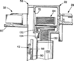
また本発明においては、周囲環境からキャリア32の内部40とロードロック22を密閉分離するために、分離ハウジングあるいは小囲い(mini-environment)58(特に図2参照)が備えられている。キャリアはある適当な方法で離れた所から運ばれ、小囲い58の一部である台60に載せられ、プロセスシステム20から離れる方向に突き出る。台60の上面62には、キャリアの底から伸びた足部66を受けるように複数の窪み64が適当な間隔で形成されている。足部66が完全に窪み64にかみ合ったときキャリア32の前面68は小囲い58の外部面70に接近している。
小囲いには通常ロードロック22と整合する、しかし離れて配置された窓72を有し、キャリアが台60に載せられたときにキャリアドア42がその窓を通して小囲いの内部へ伸びるようになっている。キャリアが台に固定されたときにキャリアと小囲い58の間には適当なシール74が設けられ、キャリアポート38と小囲いの窓72を封じ、キャリア内部、小囲い内部およびロードロックを周囲環境から分離する。図3に示すようにキャリア32が台60上に置かれたとき、小囲い58の外部面70にピボット状に取り付けられた複数の留め金300(図3A)は、キャリアの外部周辺面に設けられた留め金凹部302と選択的にかみ合うように動作する。それぞれの場合で、留め金アクチュエータ304は凹部302とかみ合う部分から離れた一端で留め金300にピボット状に取り付けられた作動ロッド306を引き伸ばしたり引っ込めたりする。信号によって留め金アクチュエータ304は留め金300が実線で示す凹部302とかみ合った位置から破線で示す凹部からはずれた位置に動くよう作動する。キャリア32の全ての留め金300が実線の位置にあるとき、シール74はキャリアと小囲いの間でしっかりと締め付けられている。
ロードロック22は実質的にパーティクルの無い室76を画定し、ロードロック室に通じたロードロックポート78を有している。前述のようにロードロック22はキャリア32と搬送室28の間に位置している。ロードロックドア80は、ロードロックポート78を覆って閉じる位置とそれから離れて開いた位置の間を移動できるようにロードロックに適切に取り付けられている。
ロードロック室76内のロードロックアーム82は、キャリア32から離れた非作動位置(図2参照)とキャリア近傍にある作動位置(図3参照)との間を動くことができる。このロードロックアームおよびその動作機構は1995年7月6日に出願され出願番号第08/498,835号が付与されて本願出願人と同一人に譲渡された本願と同時係属中の「ロードロック用搬送アーム」(パーマン アンド グリーン(Perman and Green)事件番号第390-955938-NA号)と題する特許出願に開示の構成のものでもよい。ここに上記特許出願全体を参考文献として挙げる。
図3、図4に加え図6を参照すると、多段端部エフェクタ84がロードロックアーム82の上に取り付けられている。図6でよりはっきりとわかるように、多段端部エフェクタ84は、ロードロックアーム82に載せられ上方に、特にロードロックアームにピボット状に取り付けられた関節接合88,90の一方の延長接合88から上方に突き出る搭載マニフォールド86を有している。複数の垂直方向に間隔をおいて配置された端部エフェクタの組92は搭載マニフォールドとの複合体であり、マニフォールドから外側にキャリアの方向に突き出て等間隔の平行平板の状態になる。
端部エフェクタの組92の間隔は、この説明が進むにつれて明らかになる理由でウエハの厚さよりも実質的に広い。端部エフェクタの組92はそれぞれ横方向に間隔をおいて配置された一対の端部エフェクタフィンガー94(図7参照)を有しており、水平面にウエハを保持するのに適している。複数の端部エフェクタの組92はそれぞれ搬送アームが作動位置にきたとき棚部材の組36と、つまりキャリアに保持されているウエハ34と一列になるようになっている。多段端部エフェクタ84がキャリア32に入るために、後述するような動きができるようにロードロックドア80およびキャリアドア42は開くことができ、図8に示すように離れた位置に動くことができなければならない。
したがってロードロックアーム82が作動位置にあるとき多段端部エフェクタ84は、ウエハから離れた引き込んだ位置からキャリア32の内部40へ、ロードロックポート78およびキャリアポート38を通って、ウエハを集合体として回収するように動くことができる。ロードロックアーム82は多段端部エフェクタ84を左へ(図9)動かし、端部エフェクタの組92がそれぞれウエハ34の下方でウエハとかみ合わないように動作する。多段端部エフェクタ84が左方への動きの限界点に達したときロードロックアームは多段端部エフェクタ84と共に十分な距離を上昇し、棚部材の組からウエハを集合体として持ち上げる。その後、上昇位置に保持したままでロードロックアーム82が再度動作し、多段端部エフェクタ84を右方にロードロック室76内の引き込んだ位置まで、多段端部エフェクタ84上にウエハ34の一群を載せて移動する。図11を参照のこと。
ロードロック室76内の多段端部エフェクタ84上にウエハ34の一群が位置した後は、搬送室28内の搬送アーム96はウエハ34を多段端部エフェクタから取り込み、複数のプロセス装置24の特定の1つに供給するように動作する。
多段端部エフェクタ84が上記で述べたように動作するためには、第1にキャリアドア42およびロードロックドア80の開きを調整しなければならない。この調整動作について以下に説明する。初めにキャリアドアが開けられ、次にロードロックドアが開けられ、その後両方のドアがキャリア内部とロードロック室の間の領域から離れた位置へ動く。
キャリアドアを動かす機構は、選択的にキャリアドア42とかみ合い、キャリアドアから離れロードロックドア80に隣接した第1の位置(図2)と、ロードロックドアに隣接したロードロックドアから離れた第2の位置(図3)との間を動かすことができる結合装置98を有する。第1のアクチュエータ100がロードロックドア上に取り付けられ、駆動ロッド102を介して結合装置98が第1と第2の位置との間を動くように働く。結合装置98は駆動ロッドに取り付けられたカプラ枠103、カプラ枠により支持され導かれる対向軸に配置された一対のグリップ部材104,106を有する。グリップ部材104,106はカプラ枠103により支持、導かれグリップ位置と非グリップ位置との間を動く、対向軸に配置されたグリップロッド108を有している。特にグリップ部材104,106は両端にグリップフィンガー110を有し、グリップ部材がグリップ位置にあるときグリップフィンガーはキャリアドア42の周辺リム(縁)112とかみ合う。
このようにグリップフィンガーはキャリアドア42とかみ合っていない非グリップ位置(図3)と周辺リム112とかみ合っているグリップ位置(図4)との間を動くことができる。このようなグリップ部材104,106によるキャリアドアのかみ合わせは結合装置98が第1の位置にあるときのみ起きる。カプラ枠103上の第2のアクチュエータ114はグリップ部材104,106が適切な圧力のグリップロッド108を介してグリップ位置と非グリップ位置との間を動くように働く。
キャリアドア42を開く一連の動作は、まず第1のアクチュエータ100が、グリップフィンガー110が周辺リム112の面内に入るように結合装置98をキャリアドアのごく近くまで左方に動かすことによって開始される。その後に第2のアクチュエータ114が、周辺リム112にグリップフィンガーがしっかりとかみ合うまでグリップ部材を放射状に動かし始める。その後再び第1のアクチュエータ100は、結合装置を右方に動かし内側に向いたフランジ46の端部116が、それまで周囲環境から密閉していたシール48から外れるように動作する。駆動ロッド102によって、結合装置98と、それと共にキャリアドア42がロードロックドア80に隣接した位置まで右方に動く。
ロードロックドア80に隣接した位置にキャリアドア42がある状態で、ロードロックドアの駆動機構118はロードロックドアと、それと共に結合装置98とキャリアドア42からなる部分を閉じた位置から開いた位置へ動かすよう動作する。閉じた位置ではロードロックドア80は、外気からロードロック室76を分離する適当なシール120に対ししっかりと押さえられている(図2、図12を参照)。上記はたとえば、間隔をおいて、対向した、通常は垂直な案内溝121とロードロック22,およびロードロックドア80の反対側の面によって達成される。
ロードロックドアの駆動機構118は小囲い58の底部124に取り付けられた駆動アクチュエータ122を有している。駆動アクチュエータ122は駆動アクチュエータ軸123と共に垂直に、キャリアとロードロック室76の中間に配置され、ロードロックドア80が上昇して閉じた位置と下降して開いた位置の間を動くようにロードロックドア80に適切に取り付けられている。
駆動機構118がロードロックドア、結合装置98、キャリアドア42を図8に示すように全て下げた位置になるまで多段端部エフェクタ84の動作は行われないことが理解されるであろう。
インデックス駆動機構126がロードロックアームを非作動位置(図11)と作動位置(図10)との間で動かすために設けられている。前述のようにロードロックアーム82およびその動作機構、さらにインデックス駆動機構126は1996年12月31日発行の米国特許第5,588,789号に開示の構成のものでもよい。
インデックス駆動機構126は適当なインデックスアクチュエータ軸130を伸ばすことのできる種類のインデックスアクチュエータ128を有し、粗動時は長い距離を急速に動かし、微動時には増分ステップ動作ができるものであってもよい。このようにインデックスアクチュエータは1つの動作モードとして、全ての端部エフェクタの組92がキャリア42の内部40の棚部材の組36と一直線に整列された(aligned)作動位置(図8−10)と、全ての端部エフェクタの組が棚部材の組と整列されていない非作動位置(図11)との間でロードロックアームを動かす。前者ではクラッチ132はかみ合っており、後者では外れている。
アーム駆動機構134は、ロードロックアーム82とそれと共に多段端部エフェクタ84を引き込み位置と前進位置との間で動かす適当な回転アクチュエータを有する。アーム駆動機構134はさらに、かみ合わせのできるクラッチ要素132aと132bを有し、これらはインデックス駆動機構がロードロックアームと多段端部エフェクタを作動位置に動かすときだけかみ合う。その時には前述のように端部エフェクタ84をキャリアの内部に前進させることができる。
前述したように、搬送室28の搬送アーム96は多段端部エフェクタからウエハ34を一度に取り込み複数のプロセス装置24の特定の1つに供給するように動作する。インデックス駆動機構126は、特定の端部エフェクタの組92と搬送室28内の搬送アーム96に付いているロボット端部エフェクタフィンガー138の高さを合わせるように増分モードで動作してもよい。このようにクラッチ要素132a、132bが外れて、搬送アクチュエータ140により駆動された搬送アーム96は多段端部エフェクタ84からウエハを一度に取り込み複数のプロセス装置24の特定の1つに供給するように動作する。搬送アーム96および関連する搬送アクチュエータ140はヘンドリクソン(Hendrickson)による米国特許第5,180,276号に開示の構成のものでもよい。ここに上記特許全体を参考文献として挙げる。
適当な分離バルブ30が前述のようにロードロック室76と搬送室28の間に備えられている。分離バルブは、ウエハ34を支えるロボット端部エフェクタフィンガーを通すには十分大きく、ロードロック室と搬送室の間の流体の往来を防ぎ、またある場合には許すような選択的な動作が可能である。加えて分離バルブがロードロック室と搬送室の間の流体の往来を許すような位置の時に周囲環境からロードロックと搬送室を分離するために、適当なシール142がロードロック22と搬送室28との間に挟まれている。
真空源144がロードロック室76と搬送室28を選択的に排気するために備えられている。導管146が真空源144とロードロック室の間に伸びており、導管146内の選択的動作が可能なバルブ148は、ロードロックドア80が閉じているときに真空源とロードロック室をつなぎ、ロードロックドアが開いているときにロードロック室から真空源を切り離す。同様に導管150が真空源144と搬送室の間に伸びている。導管150内の選択的動作が可能なバルブ152は、搬送室が周囲環境から分離されているときに真空源と搬送室を相互接続している。
他の望ましいキャリアドア駆動機構の実施例160について図13−15を参照する。この場合ではキャリア162は、間隔を置いて通常積み重ねた複数のウエハ34を保持し搬送する前述のキャリア32と同様である。前と同じようにキャリア162はその内部166に入ることができるようにキャリアポート164を有している。また周囲環境からロードロック室とキャリアの内部を分離、密閉する小囲い168がある。さらにキャリア162は、周囲環境から内部166を密閉するためキャリアポート164に覆い被さる閉じた位置と、キャリアポートから離れた開いた位置との間で可動なキャリアドア170を有する。
ロードロックのロードロックドア172は前述のように、周囲環境からロードロック室を密閉するためロードロックポートに覆い被さる閉じた位置と、それから離れた開いた位置との間で動くことができる。キャリアドア駆動機構とその動作はまた、前述した通りである。
小囲い168は通常ロードロックポートと整列し離れて配置された窓を有し、キャリアポート164が小囲いの窓174と近接するようにキャリア162を支持する台60を有する。適当なシール176が小囲いとキャリアの間に備えられ、キャリアが台に支持されキャリアポートと小囲いの窓を囲むときに周囲環境から小囲いの内部とロードロック室を分離する。
キャリアドア駆動機構160は、キャリアドア170と選択的にかみ合い、ロードロックドアに近くキャリアから離れた第1の位置(図13の破線で示す)と、ロードロックドアから離れキャリアに近い第2の位置(図13の実線で示す)との間を動く結合機構178を有する。第1のアクチュエータ180はロードロックドア172の上に取り付けられ、第1および第2の位置の間で結合機構178を動かす駆動ロッド182を有する。
キャリアドア170は184の所(図14および図15)で空洞になっており、その中にグリップ溝186を有する。結合機構178は駆動ロッド182に据え付けられ、結合機構が前述の第2の位置にあるときに小囲い168の窓174と係合する(窓174に収容される)ドアグリップ板188を有する。ドアグリップ板188に取り付けられたドアグリップ棒190は、キャリアドア170内のグリップ溝186を掴むようにかみ合うグリップ位置と、外れた解放位置との間を動く一対の曲がりフィンガー194をその末端に有している。
加えて、ラッチ機構196がキャリアドアに設けられ、キャリアと選択的にかみ合いキャリアドアをキャリアにしっかりと固定する。この目的のため、キャリア162はキャリアポート164内にラッチ凹部198(図14)を有する。ラッチ凹部198と共に、ラッチ機構196はラッチ凹部とかみ合ったラッチ位置とラッチ凹部から外れた非ラッチ位置との間で動く、キャリアドア170に201の所でピボット状に取り付けられたラッチ200を有する。保持ピン202は凹部184において第1端部204でラッチにピボット状に接続されており、第1端部の反対側に第2曲がり端部206を有する。曲がり端部206は一対の曲がりフィンガー194の間の溝208で受けられ、ドアグリップ棒190とかみ合うことができる。
圧縮バネ210は保持ピン202を取り囲み、凹部184内でラッチ200をラッチ位置に押し付けている。バネはその左端(図14および図15に示す)に、キャリアドア170内で凹部198の対向する両壁から突き出た肩部212で止まっている。バネ210の右端は肩部212から適度な位置で保持ピン202に固定されたC型留め具214で押し付けられている。この構成によって保持ピンおよびその第2曲がり端部206は、図13−15に見られるように右方に押し付けられている。このようにバネ210はラッチ200をラッチ凹部198とかみ合ったノーマリクローズ位置に保持するのに有効である。しかし、一対の曲がりフィンガー194をグリップ溝186を掴むようにかみ合うグリップ位置に動かすドアグリップ棒190の動きは同時にラッチをラッチ凹部から外れた位置に動かすのにも有効である。グリップ溝186とかみ合う曲がりフィンガー194を保持し、ラッチ200を開位置に保持する(全て図14に示されている)アクチュエータ192の連続的な動作で、キャリアドア170とドアグリップ板188は一体となり、アクチュエータ180によって図13で破線で示す開位置へ動かすことができる。
本発明の望ましい実施態様について詳細に説明したが、当業者であれば本明細書および請求の範囲に記載された本発明の範囲から逸脱せずに様々な変形が可能であることは理解できるであろう。Background of the Invention
1. TECHNICAL FIELD OF THE INVENTION
The present invention relates to a standardized mechanism interface for reducing particle contamination, and more particularly to an apparatus for preventing particle contamination using a sealed container of a semiconductor processing apparatus. Furthermore, the present invention particularly relates to a system for efficiently transferring a semiconductor wafer between a load lock chamber capable of environmental control waiting for transfer to a processing facility such as a cluster apparatus and a transfer container or carrier. The present invention can greatly improve the throughput of the manufacturing process.
In the present disclosure, the term “wafer” is consistently used to refer to a planar substrate such as a silicon wafer or a flat glass panel, but is intended to have a broad meaning that applies to all substrates. Usually, such a substrate is circular and has a diameter of 200 mm and a thickness of about 0.760 mm, but recently has evolved to 300 mm with the same thickness.
2. Conventional technology
Control of particulate contamination is essential for VLSI circuit manufacturing in terms of cost, high yield, and high profitability. Smaller line and space design rules have been demanded, and there is an increasing need to control the number of particles and remove even smaller particles.
Contaminated particles can cause incomplete etching between lines and form unwanted bridges. In addition to such physical defects, there is particle contamination that causes electrical defects due to ions and trap centers in gate junctions and dielectrics.
The main sources of particle contamination are people, equipment and chemicals. Human-generated particles are transferred through the environment, physical contact, and migration to the wafer surface. For example, humans are a significant source of particles because peeled skin is easily ionized and produces defects.
Modern processing equipment is concerned with particles ranging from 0.01 microns or less to sizes of 200 microns. Particles of these sizes are very damaging in semiconductor processes. Today's normal semiconductor processes use sizes below 1 micron. Contaminating particles having a size of 0.1 microns or more actually impede the semiconductor device using 1 micron. Of course, as a trend, the size of the semiconductor process is getting smaller.
In recent years, “clean rooms” have been established by filters and other techniques, and attempts have been made to remove particles larger than 0.03 microns. But the process environment needs to be improved. The conventional “clean room” cannot maintain the desired particle-free state. In the conventional “clean room”, it is practically impossible to maintain a state of no particles of 0.01 μm or less. Dust-free garments reduce particle emissions, but cannot hold particles completely. Even a fully dressed worker is 0.028m per minute Three It is known that 6000 particles are released close to itself per cubic foot.
The industry trend to control contaminating particles is to build a more elaborate (and expensive) clean room with HEPA and ULPA air circulation systems. In order to obtain an acceptable level of cleanliness, the filter efficiency requires a complete air exchange of 99.999% or more per minute.
Particles in equipment and chemicals are called “process defects”. To minimize process defects, process equipment manufacturers must prevent generated particles from reaching the wafer, and gas and liquid chemical suppliers must provide cleaner products. . The most important is to effectively separate the wafer from the particles when the wafer is stored, transported and transferred to the process equipment.
A standard mechanical interface (SMIF) system has been devised and used to greatly reduce the amount of particles on the wafer and reduce particle contamination. During storage, transportation, and processing of the wafer, the gas medium (air, nitrogen, etc.) around the wafer is mechanically stationary with respect to the wafer so that particles do not immediately enter the wafer environment from the outside atmosphere. This purpose is achieved.
The SMIF concept is that the cleanest environment for a wafer is a small, stationary volume with no particles and no internal source of particles.
Typically, SMIF systems use (1) a dust-proof box or carrier with a minimum volume for storage and transportation, (2) a wafer cassette with a release shelf, and (3) the box or carrier door is designed to match the port of the process equipment Thus, the two doors can be opened at the same time, and the particles on the outer surface of the door are captured ("sandwiched") between the doors.
In a normal SMIF system, the box or carrier is placed at the interface port and at the location of the box door and a latch that opens the port door simultaneously. A mechanical elevator lowers the door and the cassette rides on the top. A manipulator picks up the cassette and places it on the cassette port / elevator of the device. The reverse operation is performed after the process.
The SMIF system has been experimented with inside and outside a clean room and has proven effective. This SMIF is a 10-fold improvement over the conventional method of handling a release cassette in a clean room.
By using the SMIF system, it has become common to hold wafers apart by a cassette and carry multiple wafers in boxes or carriers. In this technique, wafers are placed on a cassette, the cassettes are transported into boxes or cassettes, and then one by one removed from the cassette and placed in a receiving chamber or other process equipment of the cluster apparatus. Recently, cassettes have been replaced by more efficient and particle-free cassettes that can transport multiple wafers simultaneously.
From the foregoing prior art, the present invention is understood and put into practice. In particular, the present invention maintains a clean room environment and transports a large number of wafers at the same time, while inventorying equipment, that is, reducing initial costs, being simple and small, having low maintenance costs, and improving process throughput. . Much of the foregoing has been related to the SMIF system and control of the environment in which the wafer is handled, but it can be widely applied to aspects of handling materials, such as the environment to which the wafer of the present invention is exposed.
Summary of the Invention
The present invention is a system for batch loading semiconductor wafers onto a load lock from a portable carrier that separates and stacks a plurality of wafers and transports them to a particle-free environment. The carrier is supported adjacent to a load lock chamber having a particle free environment. The multi-stage end effector (effector) associated with the load lock chamber has a plurality of end effector sets, each set being arranged to align with a corresponding wafer in the carrier to hold the wafer. It has become. Wafers can be taken out as a group, held in the load lock chamber for the next transfer, sent to the next transfer chamber at a time, and supplied to a plurality of specific process devices in the cluster system . A separate housing or enclosure seals and separates the load lock chamber and carrier interior from the surrounding environment. After the plurality of wafers are transferred from the carrier to the load lock chamber, the carrier and the load lock chamber are sealed, and the load lock chamber and the transfer chamber are exhausted. Various mechanisms for moving the end effector set, ie, a lifting mechanism for entering and exiting the carrier and load lock chamber, closed and open positions with the carrier door and load lock door sealed, and the carrier and load lock chamber A mechanism for moving to a stop position away from the space is provided. Furthermore, a mechanism for moving the carrier door and the load lock door individually between the sealed closed position and the open position and moving them together to a stop position away from between the carrier and the load lock chamber is provided. .
The present invention provides an interface for sending a wafer carrier to a load lock while maintaining a clean environment for the substrate carrier. The present invention provides an efficient, fast operation, unified design that maximizes process throughput while protecting from the external environment during process step execution.
Since the load lock arm has a batch end effector functioning as a cassette, which is inherently structurally unconstrained, no elevator is required for wafer transfer. Gas contamination from the cassette (usually outgassing polymer) has also been removed, improving the quality of the wafer process. In addition, the arm assembly is mainly made of metal that emits a minimum amount of gas, and the degree of vacuum is improved in a short time.
The present invention provides a unified carrier and cassette structure that does not require unnecessary cassettes and their inventory. Like the conventional SMIF loader that lowers the cassette from the SMIF box and transports it to the load lock, it removes the danger of transporting the wafer in air and exposing it to particle contamination. In the example of the present invention, since the wafers are loaded in a batch configuration, the indirect time can be reduced and high throughput is obtained.
Further features, advantages, and benefits of the present invention will become more apparent from the following description and drawings. The foregoing summary and the following detailed description are exemplary and explanatory and are not restrictive of the invention. Together with the detailed description, the accompanying drawings, which illustrate one embodiment of the invention and form a part of the invention, serve to generally explain the principles of the invention. Similarly, numbers throughout this disclosure refer to similar parts.
[Brief description of the drawings]
FIG. 1 is a schematic top view showing a state in which a cover is removed from a transfer chamber of a wafer processing system according to the present invention.
FIG. 2 is a side elevational view showing certain parts shown in FIG. 1 in detail, with some parts shown in cross-section for clarity.
FIG. 3 is a schematic detailed side elevational view, where some parts are shown in cross-section or omitted for clarity, and some parts of FIG. 2 will be described in detail, with the carrier door in a closed position. Show.
FIG. 3A is a cross-sectional view illustrating in detail a minute portion of FIG.
FIG. 4 is a schematic side elevational view showing a portion of FIG. 2 when the carrier door is in the open position.
FIG. 5 is a perspective view illustrating in detail the parts of FIG. 3 with certain parts shown in cross-section for clarity.
FIG. 6 is a side elevational view showing a portion of FIG. 2 in detail.
7 is a cross-sectional view taken along line 7-7 of FIG.
8, 9, 10 and 11 are schematic side elevational views similar to FIG. 4 illustrating the continuous relative position of the parts.
FIG. 12 is a detailed perspective view illustrating the part of FIG. 2 in more detail.
FIG. 13 is a detailed top plan view of an enlarged section showing another embodiment of the present invention.
FIG. 14 is a more detailed top plan view illustrating in more detail components at other positions in FIG.
FIG. 15 is a detailed perspective view of FIG. 14, showing a cross-section with a portion cut away.
Detailed Description of the Invention
Referring to the drawings, FIG. 1 first shows a
The
As mentioned above, now transportable SMIF boxes or containers, here called “carriers”, are known to be used to keep semiconductor wafers and the like clean. The wafer is kept clean by taking it in and out of the
According to the present invention, as shown in FIGS. 2 and 3, a deformable
The
Extending from the
In the present invention, a separation housing or mini-environment 58 (see particularly FIG. 2) is provided to hermetically separate the inside 40 of the
The enclosure usually has a
The
The
Referring to FIG. 6 in addition to FIGS. 3 and 4, a
The spacing between the end effector sets 92 is substantially wider than the wafer thickness for reasons that will become apparent as this description proceeds. Each end effector set 92 has a pair of end effector fingers 94 (see FIG. 7) spaced laterally apart, and is suitable for holding a wafer in a horizontal plane. Each of the plurality of end effector sets 92 is aligned with the shelf member set 36, that is, the
Thus, when the
After the group of
In order for the
The mechanism for moving the carrier door selectively engages the
In this manner, the grip fingers can move between a non-grip position (FIG. 3) that is not engaged with the
A series of actions to open the
With the
The load lock
It will be appreciated that the
An
The
The
As described above, the
A
A
13-15 for another preferred carrier door
As described above, the
The
The carrier
The
In addition, a
The
Although preferred embodiments of the present invention have been described in detail, those skilled in the art will recognize that various modifications can be made without departing from the scope of the invention as set forth in the specification and claims. I will.
Claims (8)
前記システムは、
実質的にパーティクルの無い環境において、間隔を置いて積み重ねた複数の半導体ウエハを支えつつ搬送する可搬型キャリアと、
実質的にパーティクルの無い環境を有するロードロック室を画定するロードロックと、
前記ロードロックと前記キャリアの間に設けられ、前記ロードロック室および前記キャリアの内部を周囲環境から密閉して分離する分離ハウジングと、からなり、
前記ロードロックは前記ロードロック室に通じたロードロックポートを有し、
前記可搬型キャリアは、自身の内部へのアクセスを可能にするキャリアポートを有し、
前記アセンブリは、
前記キャリアに設けられ、前記キャリアポートを覆い前記周囲環境から前記キャリアの内部を密閉するキャリア閉位置と前記キャリアポートと間隔を置いたキャリア開位置との間を動き得るキャリアドアと、
前記ロードロックに設けられ、前記ロードロックポートを覆い前記周囲環境から前記ロードロック室を密閉するロードロック閉位置と前記ロードロックポートと間隔を置いたロードロック開位置との間を動き得るロードロックドアと、
前記ロードロックドアに設けられ、前記キャリア閉位置と前記キャリア開位置の間で前記キャリアドアを動かすキャリアドア駆動機構と、を含み、
前記分離ハウジングは前側の窓と後側の窓を有し、前記後側の窓は前記ロードロックポートと間隔を置いて整列しており、
前記分離ハウジングは、前記キャリアポートが前記前側の窓に接近するよう前記キャリアを支持する台を有し、前記半導体ウエハは前記キャリアから前記前側の窓を通って前記分離ハウジングに入ることができ、且つ、前記半導体ウエハは前記後側の窓から前記ロードロックに入ることができ、
前記アセンブリはさらに、
前記キャリアが前記台に支持されたときに前記分離ハウジングと前記キャリアの間に位置し、前記周囲環境から前記キャリアの内部及び前記分離ハウジングの内部をシールするシール手段を含み、
前記ロードロックドアが前記ロードロック閉位置からロードロック開位置へ動く方向は、前記半導体ウエハが前記キャリアから前記分離ハウジングを通って前記ロードロックに移動する方向と直交していることを特徴とするアセンブリ。A transfer delivery assembly used in combination with a system for batch loading semiconductor wafers,
The system
In substantially no particle environment, and portable carrier we send transportable while supporting a plurality of semiconductor wafers stacked at intervals,
A load lock defining a load lock chamber having a substantially particle-free environment;
A separation housing that is provided between the load lock and the carrier and seals and separates the load lock chamber and the inside of the carrier from the surrounding environment;
The load lock has a load lock port leading to the load lock chamber;
The portable carrier has a carrier port allowing access to its interior;
The assembly is
A carrier door which is provided on the carrier and which can move between a carrier closed position which covers the carrier port and seals the inside of the carrier from the surrounding environment and a carrier open position spaced apart from the carrier port;
A load lock provided on the load lock and movable between a load lock closed position that covers the load lock port and seals the load lock chamber from the surrounding environment and a load lock open position spaced apart from the load lock port. Door,
A carrier door drive mechanism provided on the load lock door and moving the carrier door between the carrier closed position and the carrier open position;
The separation housing has a front window and a rear window, the rear window being aligned with a distance from the load lock port;
Before SL separation housing has a base which said carrier port supports the carrier so as to approach the front of the window, the semiconductor wafer can enter the separating housing through the front window from the carrier And the semiconductor wafer can enter the load lock from the rear window,
Before Symbol assembly further,
The separation housing and located between the carrier, before Symbol viewed including the internal and sealing means for sealing the interior of the separation housing of the carrier from the ambient environment when said carrier is supported on said platform,
The direction in which the load lock door moves from the load lock closed position to the load lock open position is orthogonal to the direction in which the semiconductor wafer moves from the carrier through the separation housing to the load lock. assembly.
前記キャリアドアに係合可能であり、前記キャリアドアから離れ前記ロードロックドアに隣接した第1の位置と、前記キャリアドアに隣接し前記ロードロックドアから離れた第2の位置との間を動くことができる結合手段と、
前記ロードロックドアに設けられ、前記第1の位置と前記第2の位置との間で前記結合手段を動かす第1アクチュエータと、を有し、
前記結合手段は、前記結合手段が前記第2の位置にあるとき、前記キャリアドアに係合しない非グリップ位置と前記キャリアドアに係合するグリップ位置との間を動くことができるグリップ部材を有し、
前記キャリアドア駆動機構はさらに、前記非グリップ位置と前記グリップ位置との間で前記グリップ部材を動かす第2アクチュエータを有することを特徴とするアセンブリ。The assembly of claim 1, wherein the carrier door drive mechanism is
Engageable with the carrier door and moves between a first position away from the carrier door and adjacent to the load lock door and a second position adjacent to the carrier door and away from the load lock door. A coupling means capable of,
A first actuator provided on the load lock door and moving the coupling means between the first position and the second position;
It said coupling means, when the front Symbol coupling means is in said second position, the gripping member is movable between a gripping position engaging the non-gripping position not engaging the carrier door to the carrier door Have
The carrier door drive mechanism further comprises a second actuator for moving the grip member between the non-grip position and the grip position.
前記第1アクチュエータが前記第1および第2の位置の間で前記結合手段を動かす駆動ロッドを有し、
前記結合手段が前記駆動ロッドに取り付けられた結合器枠を有し、
前記グリップ部材が対向配置されたグリップロッドを有し、当該グリップロッドは前記結合器枠により軸方向に整列するように保持され、且つ、前記非グリップ位置と前記グリップ位置との間で動くように導かれ、前記グリップ部材のそれぞれが端部に横方向グリップフィンガーを有し、
前記グリップフィンガーがグリップ位置にあるとき前記グリップフィンガーは前記周辺リムと係合することを特徴とするアセンブリ。The assembly of claim 2, wherein the carrier door has a peripheral rim;
The first actuator has a drive rod that moves the coupling means between the first and second positions;
The coupling means comprises a coupler frame attached to the drive rod;
The grip member has a grip rod oppositely disposed, the grip rod is held in axial alignment by the coupler frame, and is moved between the non-grip position and the grip position. Each of the gripping members has a lateral gripping finger at the end;
The assembly wherein the grip finger engages the peripheral rim when the grip finger is in a grip position.
前記ロードロック閉位置と前記ロードロック開位置の間で前記ロードロックドアを動かすロードロックドア駆動機構を有することを特徴とするアセンブリ。The assembly of claim 1, comprising:
An assembly comprising a load lock door drive mechanism for moving the load lock door between the load lock closed position and the load lock open position.
前記ロードロックドアを前記ロードロック閉位置と前記ロードロック開位置との間で動かすロードロックドア駆動機構を有し、
前記ロードロックドアが前記ロードロック開位置へ動く際に、前記ロードロックドア駆動機構は前記ロードロックドアと一体的に前記結合手段および前記キャリアドアを動かすことを特徴とするアセンブリ。The assembly of claim 3, comprising:
A load lock door drive mechanism for moving said load lock door between the Rodoro' click open position and the Rodoro' click closed position,
When prior Symbol load lock door is moved to the load lock open position, the load lock door drive mechanism assembly, characterized in that moving said coupling means and said carrier door the load lock door and integrally.
前記キャリアドアがグリップ溝を有し、
前記第1アクチュエータが前記第1の位置と前記第2の位置との間で前記結合手段を動かす駆動ロッドを有し、
前記結合手段がドアグリップ板とドアグリップ棒とを有し、
前記ドアグリップ板は前記駆動ロッドに取り付けられ、前記結合手段が前記第2の位置にあるときに前記分離ハウジングの前側の窓に嵌合し、
前記ドアグリップ棒は前記第2アクチュエータに取り付けられ、前記キャリアドア内の前記グリップ溝に係合するグリップ位置と、係合が外れる解放位置との間を動き、末端に一対の曲がりフィンガーを有することを特徴とするアセンブリ。The assembly of claim 2, comprising:
The carrier door has a grip groove ;
Wherein the first actuator includes a drive rod for moving said coupling means between said first position and the second position,
The coupling means includes a door grip plate and a door grip rod;
The door grip plate is attached to the drive rod and engages a front window of the separation housing when the coupling means is in the second position;
The door grip rod is attached to the second actuator and moves between a grip position engaging with the grip groove in the carrier door and a release position where the engagement is released, and has a pair of bending fingers at the end. An assembly featuring.
前記キャリアドア上に、前記キャリアと係合して前記キャリアドアを前記キャリアに固定するラッチ手段を有することを特徴とするアセンブリ。The assembly of claim 6, comprising:
An assembly comprising: latch means on the carrier door for engaging the carrier and securing the carrier door to the carrier.
前記キャリアが前記キャリアポート内にラッチ凹部を有し、
前記ラッチ手段が、
前記キャリアドアにピボット状に取り付けられ、前記ラッチ凹部に係合するラッチ位置と前記ラッチ凹部から外れた非ラッチ位置との間で動くラッチと、
前記ラッチにピボット状に接続され、前記キャリアドア内に第1端部を有し、前記第1端部の反対側に第2曲がり端部を有し、前記曲がり端部が前記一対の曲がりフィンガーの間に係合し前記ドアグリップ棒と係合する保持ピンと、
前記ラッチを前記ラッチ位置に押し付ける弾性手段と、からなり
前記一対の曲がりフィンガーを前記グリップ溝に係合させる前記グリップ位置に動かす前記ドアグリップ棒の動きによって、同時に前記ラッチを前記ラッチ凹部から外れた前記非ラッチ位置に動かすことを特徴とするアセンブリ。The assembly according to claim 7, comprising:
The carrier has a latch recess in the carrier port;
The latch means;
A latch pivotally attached to the carrier door and moving between a latch position engaging the latch recess and a non-latching position disengaged from the latch recess;
The latch is pivotally connected, has a first end in the carrier door, has a second bent end on the opposite side of the first end, and the bent end is the pair of bent fingers. A retaining pin that engages between and engages the door grip bar;
Elastic means for pressing the latch against the latch position, and the movement of the door grip rod that moves the pair of bending fingers to the grip position to engage with the grip groove simultaneously releases the latch from the latch recess. The assembly is moved to the non-latching position.
Applications Claiming Priority (9)
| Application Number | Priority Date | Filing Date | Title |
|---|---|---|---|
| US49898795A | 1995-07-06 | 1995-07-06 | |
| US08/498,597 | 1995-07-06 | ||
| US08/499,069 | 1995-07-06 | ||
| US08/499,069 US5613821A (en) | 1995-07-06 | 1995-07-06 | Cluster tool batchloader of substrate carrier |
| US08/498,859 | 1995-07-06 | ||
| US08/498,859 US5607276A (en) | 1995-07-06 | 1995-07-06 | Batchloader for substrate carrier on load lock |
| US08/498,987 | 1995-07-06 | ||
| US08/498,597 US5609459A (en) | 1995-07-06 | 1995-07-06 | Door drive mechanisms for substrate carrier and load lock |
| PCT/US1996/011244 WO1997002199A1 (en) | 1995-07-06 | 1996-07-02 | Door drive mechanisms for substrate carrier and load lock |
Publications (2)
| Publication Number | Publication Date |
|---|---|
| JPH11513006A JPH11513006A (en) | 1999-11-09 |
| JP4306798B2 true JP4306798B2 (en) | 2009-08-05 |
Family
ID=27504398
Family Applications (1)
| Application Number | Title | Priority Date | Filing Date |
|---|---|---|---|
| JP50529197A Expired - Lifetime JP4306798B2 (en) | 1995-07-06 | 1996-07-02 | Substrate carrier and load lock door drive device |
Country Status (7)
| Country | Link |
|---|---|
| EP (1) | EP0886617A1 (en) |
| JP (1) | JP4306798B2 (en) |
| KR (1) | KR19990028767A (en) |
| CN (1) | CN1195332A (en) |
| AU (1) | AU6408996A (en) |
| TW (1) | TW278200B (en) |
| WO (1) | WO1997002199A1 (en) |
Cited By (2)
| Publication number | Priority date | Publication date | Assignee | Title |
|---|---|---|---|---|
| KR102200250B1 (en) * | 2020-05-29 | 2021-01-11 | 주식회사 싸이맥스 | Load port module provided with a Foup loadlock door, and a method for opening and closing the Load port module door and the Foup loadlock door |
| KR102247183B1 (en) * | 2020-05-29 | 2021-05-04 | 주식회사 싸이맥스 | Wafer processing equipment with efficient installation area |
Families Citing this family (14)
| Publication number | Priority date | Publication date | Assignee | Title |
|---|---|---|---|---|
| SG47226A1 (en) * | 1996-07-12 | 1998-03-20 | Motorola Inc | Method and apparatus for transporting and using a semiconductor substrate carrier |
| US6280134B1 (en) | 1997-06-17 | 2001-08-28 | Applied Materials, Inc. | Apparatus and method for automated cassette handling |
| DE19805624A1 (en) * | 1998-02-12 | 1999-09-23 | Acr Automation In Cleanroom | Lock for opening and closing clean room transport boxes |
| US6610150B1 (en) * | 1999-04-02 | 2003-08-26 | Asml Us, Inc. | Semiconductor wafer processing system with vertically-stacked process chambers and single-axis dual-wafer transfer system |
| JP4628530B2 (en) * | 2000-08-25 | 2011-02-09 | 株式会社ライト製作所 | Transport container lid attaching / detaching device |
| SG115630A1 (en) * | 2003-03-11 | 2005-10-28 | Asml Netherlands Bv | Temperature conditioned load lock, lithographic apparatus comprising such a load lock and method of manufacturing a substrate with such a load lock |
| KR101131417B1 (en) * | 2003-11-12 | 2012-04-03 | 주성엔지니어링(주) | Loadlock and loadlock chamber using the same |
| JP4748816B2 (en) * | 2008-11-28 | 2011-08-17 | Tdk株式会社 | Closed container lid opening and closing system |
| JP5279576B2 (en) * | 2009-03-27 | 2013-09-04 | 大日本スクリーン製造株式会社 | Substrate processing equipment |
| JP4919123B2 (en) | 2010-03-08 | 2012-04-18 | Tdk株式会社 | Processing substrate storage pod and lid opening / closing system of processing substrate storage pod |
| US10741432B2 (en) * | 2017-02-06 | 2020-08-11 | Applied Materials, Inc. | Systems, apparatus, and methods for a load port door opener |
| US10510573B2 (en) * | 2017-11-14 | 2019-12-17 | Taiwan Semiconductor Manufacturing Co., Ltd. | Loading apparatus and operating method thereof |
| US11302553B1 (en) * | 2021-01-07 | 2022-04-12 | Taiwan Semiconductor Manufacturing Company, Ltd. | Transport carrier docking device |
| CN114777490B (en) * | 2022-06-21 | 2022-09-09 | 上海陛通半导体能源科技股份有限公司 | Semiconductor device capable of realizing automatic omnidirectional opening and closing |
Family Cites Families (4)
| Publication number | Priority date | Publication date | Assignee | Title |
|---|---|---|---|---|
| US4550242A (en) * | 1981-10-05 | 1985-10-29 | Tokyo Denshi Kagaku Kabushiki Kaisha | Automatic plasma processing device and heat treatment device for batch treatment of workpieces |
| JPH0461146A (en) * | 1990-06-22 | 1992-02-27 | Mitsubishi Electric Corp | Shifter for semiconductor wafer |
| JPH04206547A (en) * | 1990-11-30 | 1992-07-28 | Hitachi Ltd | Transfer method between devices |
| JP3275390B2 (en) * | 1992-10-06 | 2002-04-15 | 神鋼電機株式会社 | Portable closed container circulation type automatic transfer system |
-
1995
- 1995-09-07 TW TW084109347A patent/TW278200B/en active
-
1996
- 1996-07-02 AU AU64089/96A patent/AU6408996A/en not_active Abandoned
- 1996-07-02 CN CN96196791A patent/CN1195332A/en active Pending
- 1996-07-02 WO PCT/US1996/011244 patent/WO1997002199A1/en not_active Ceased
- 1996-07-02 EP EP96923623A patent/EP0886617A1/en not_active Withdrawn
- 1996-07-02 KR KR1019980700066A patent/KR19990028767A/en not_active Abandoned
- 1996-07-02 JP JP50529197A patent/JP4306798B2/en not_active Expired - Lifetime
Cited By (2)
| Publication number | Priority date | Publication date | Assignee | Title |
|---|---|---|---|---|
| KR102200250B1 (en) * | 2020-05-29 | 2021-01-11 | 주식회사 싸이맥스 | Load port module provided with a Foup loadlock door, and a method for opening and closing the Load port module door and the Foup loadlock door |
| KR102247183B1 (en) * | 2020-05-29 | 2021-05-04 | 주식회사 싸이맥스 | Wafer processing equipment with efficient installation area |
Also Published As
| Publication number | Publication date |
|---|---|
| EP0886617A1 (en) | 1998-12-30 |
| AU6408996A (en) | 1997-02-05 |
| CN1195332A (en) | 1998-10-07 |
| JPH11513006A (en) | 1999-11-09 |
| WO1997002199A1 (en) | 1997-01-23 |
| TW278200B (en) | 1996-06-11 |
| KR19990028767A (en) | 1999-04-15 |
Similar Documents
| Publication | Publication Date | Title |
|---|---|---|
| US5664925A (en) | Batchloader for load lock | |
| US5609459A (en) | Door drive mechanisms for substrate carrier and load lock | |
| US5613821A (en) | Cluster tool batchloader of substrate carrier | |
| US5607276A (en) | Batchloader for substrate carrier on load lock | |
| US6120229A (en) | Substrate carrier as batchloader | |
| US5752796A (en) | Vacuum integrated SMIF system | |
| JP4306798B2 (en) | Substrate carrier and load lock door drive device | |
| JP5244097B2 (en) | Device with transport pod and interface for substrates | |
| USRE43023E1 (en) | Dual loading port semiconductor processing equipment | |
| US6517304B1 (en) | Method for transporting substrates and a semiconductor manufacturing apparatus using the method | |
| EP0980585B1 (en) | Multiple single-wafer loadlock wafer processing apparatus and loading and unloading method therefor | |
| US6176023B1 (en) | Device for transporting flat objects and process for transferring said objects between said device and a processing machine | |
| US6042623A (en) | Two-wafer loadlock wafer processing apparatus and loading and unloading method therefor | |
| JP3417821B2 (en) | Clean box, clean transfer method and device | |
| US4859137A (en) | Apparatus for transporting a holder between a port opening of a standardized mechanical interface system and a loading and unloading station | |
| KR20010020944A (en) | Load-lock with external staging area | |
| JPH0746694B2 (en) | Interface device between two sealed environments | |
| US20080219816A1 (en) | Small lot loadport configurations | |
| KR20240096824A (en) | stalker system | |
| KR20230024415A (en) | Batch wafer degassing chamber, and integration into factory interfaces and vacuum-based mainframes | |
| JP4359109B2 (en) | Substrate processing apparatus and substrate processing method | |
| KR20030065275A (en) | Substrate container with non-friction door element | |
| JP3461140B2 (en) | Clean box, clean transfer method and system | |
| JP3400382B2 (en) | Clean box, clean transfer method and system | |
| KR20010098420A (en) | Foup structure and substrate accommodating jig delivery device |
Legal Events
| Date | Code | Title | Description |
|---|---|---|---|
| A131 | Notification of reasons for refusal |
Free format text: JAPANESE INTERMEDIATE CODE: A131 Effective date: 20060613 |
|
| A601 | Written request for extension of time |
Free format text: JAPANESE INTERMEDIATE CODE: A601 Effective date: 20060911 |
|
| A602 | Written permission of extension of time |
Free format text: JAPANESE INTERMEDIATE CODE: A602 Effective date: 20061030 |
|
| A521 | Request for written amendment filed |
Free format text: JAPANESE INTERMEDIATE CODE: A523 Effective date: 20061211 |
|
| A02 | Decision of refusal |
Free format text: JAPANESE INTERMEDIATE CODE: A02 Effective date: 20070213 |
|
| A521 | Request for written amendment filed |
Free format text: JAPANESE INTERMEDIATE CODE: A523 Effective date: 20070611 |
|
| A911 | Transfer to examiner for re-examination before appeal (zenchi) |
Free format text: JAPANESE INTERMEDIATE CODE: A911 Effective date: 20070628 |
|
| A912 | Re-examination (zenchi) completed and case transferred to appeal board |
Free format text: JAPANESE INTERMEDIATE CODE: A912 Effective date: 20080228 |
|
| A601 | Written request for extension of time |
Free format text: JAPANESE INTERMEDIATE CODE: A601 Effective date: 20080811 |
|
| A601 | Written request for extension of time |
Free format text: JAPANESE INTERMEDIATE CODE: A601 Effective date: 20080818 |
|
| A602 | Written permission of extension of time |
Free format text: JAPANESE INTERMEDIATE CODE: A602 Effective date: 20080821 |
|
| A521 | Request for written amendment filed |
Free format text: JAPANESE INTERMEDIATE CODE: A523 Effective date: 20081120 |
|
| A521 | Request for written amendment filed |
Free format text: JAPANESE INTERMEDIATE CODE: A523 Effective date: 20081211 |
|
| RD13 | Notification of appointment of power of sub attorney |
Free format text: JAPANESE INTERMEDIATE CODE: A7433 Effective date: 20090114 |
|
| RD03 | Notification of appointment of power of attorney |
Free format text: JAPANESE INTERMEDIATE CODE: A7423 Effective date: 20090123 |
|
| A521 | Request for written amendment filed |
Free format text: JAPANESE INTERMEDIATE CODE: A523 Effective date: 20090313 |
|
| A01 | Written decision to grant a patent or to grant a registration (utility model) |
Free format text: JAPANESE INTERMEDIATE CODE: A01 |
|
| A61 | First payment of annual fees (during grant procedure) |
Free format text: JAPANESE INTERMEDIATE CODE: A61 Effective date: 20090428 |
|
| R150 | Certificate of patent or registration of utility model |
Free format text: JAPANESE INTERMEDIATE CODE: R150 |
|
| FPAY | Renewal fee payment (event date is renewal date of database) |
Free format text: PAYMENT UNTIL: 20120515 Year of fee payment: 3 |
|
| FPAY | Renewal fee payment (event date is renewal date of database) |
Free format text: PAYMENT UNTIL: 20130515 Year of fee payment: 4 |
|
| R250 | Receipt of annual fees |
Free format text: JAPANESE INTERMEDIATE CODE: R250 |
|
| R250 | Receipt of annual fees |
Free format text: JAPANESE INTERMEDIATE CODE: R250 |
|
| R250 | Receipt of annual fees |
Free format text: JAPANESE INTERMEDIATE CODE: R250 |
|
| R250 | Receipt of annual fees |
Free format text: JAPANESE INTERMEDIATE CODE: R250 |
|
| EXPY | Cancellation because of completion of term |