JP4286853B2 - Electronics - Google Patents
Electronics Download PDFInfo
- Publication number
- JP4286853B2 JP4286853B2 JP2006237381A JP2006237381A JP4286853B2 JP 4286853 B2 JP4286853 B2 JP 4286853B2 JP 2006237381 A JP2006237381 A JP 2006237381A JP 2006237381 A JP2006237381 A JP 2006237381A JP 4286853 B2 JP4286853 B2 JP 4286853B2
- Authority
- JP
- Japan
- Prior art keywords
- light
- guide plate
- light guide
- display screen
- touch panel
- Prior art date
- Legal status (The legal status is an assumption and is not a legal conclusion. Google has not performed a legal analysis and makes no representation as to the accuracy of the status listed.)
- Expired - Fee Related
Links
Images


Classifications
-
- G—PHYSICS
- G06—COMPUTING; CALCULATING OR COUNTING
- G06F—ELECTRIC DIGITAL DATA PROCESSING
- G06F2203/00—Indexing scheme relating to G06F3/00 - G06F3/048
- G06F2203/041—Indexing scheme relating to G06F3/041 - G06F3/045
- G06F2203/04109—FTIR in optical digitiser, i.e. touch detection by frustrating the total internal reflection within an optical waveguide due to changes of optical properties or deformation at the touch location
Landscapes
- Position Input By Displaying (AREA)
Description
本発明は、ペン先又は指先等による入力位置を光センサーにより検出するタッチパネル及びタッチパネルを備えた電子機器に関するものである。 The present invention relates to a touch panel that detects an input position of a pen tip or a fingertip with an optical sensor and an electronic device including the touch panel.
従来、タッチパネルには、パネル全面に感圧式、静電容量式のセンサーが形成されており、パネル面をペンや指先で触れることにより、ペン先又は指先の位置をセンサーで検出している。しかしながら、このようなタッチパネルでは、パネル全面にセンサーを設けるため、製造が困難であり、また、機械的な強度に問題がある。 2. Description of the Related Art Conventionally, a touch panel has a pressure-sensitive and capacitive sensor formed on the entire surface of the panel, and the position of the pen tip or fingertip is detected by the sensor by touching the panel surface with a pen or fingertip. However, such a touch panel is difficult to manufacture because a sensor is provided on the entire surface of the panel, and there is a problem in mechanical strength.
そこで、上記の問題点を解消したタッチパネルとして、発光素子と受光素子とをパネル周囲に対向して設けられた光学式(又は光電式)のタッチパネルが知られている。図8に光学式のタッチパネルを簡単に示す。図8(A)は上面図であり、図8(B)は図(A)の一点鎖線A−A'に沿った断面図である。 Therefore, an optical (or photoelectric) touch panel in which a light emitting element and a light receiving element are provided facing the periphery of the panel is known as a touch panel that solves the above problems. FIG. 8 simply shows an optical touch panel. FIG. 8A is a top view, and FIG. 8B is a cross-sectional view taken along one-dot chain line AA ′ in FIG.
図8に示すように、パネル11の1辺に発光素子12a〜12eがライン状に配列され、これに対向する辺に受光素子13a〜13eがライン状に配列されている。パネル11を指で触れると、触れた位置で発光素子12bからの光が遮断されるため、これと対向している受光素子13bの出力信号が減少する。即ち、指先が触れた位置が、出力信号が減少した受光素子の位置として検出される。
As shown in FIG. 8, the light emitting elements 12a to 12e are arranged in a line on one side of the
しかしながら、図8の光学式タッチパネルでは、光が空気中を伝搬するため、外光の影響を受け易い。また発光素子12、受光素子13の表面が汚れやすいという欠点も有する。この欠点を改善したタッチパネルの1つが特開平7−253853号公報に開示されている。
However, the optical touch panel of FIG. 8 is susceptible to the influence of external light because light propagates through the air. Further, there is a drawback that the surfaces of the
図9に示すように、特開平7−253853号公報では、異方性透明結晶よりなる押し変形自在なパネル21の側面に発光素子22がライン状に配置され、これと対向する側面に受光素子23がライン状に配置されている。発光素子22、受光素子23がパネル21側面に密接して設けられているため、汚れの影響が受けにくくなっている。
As shown in FIG. 9, in Japanese Patent Application Laid-Open No. 7-253853, a light emitting element 22 is arranged in a line on the side surface of a push-
発光素子22からの出射光は光路イに沿って進み、受光素子23に受光される。パネル21を指で押すと押された部分が歪むため、発光素子22から出射光は光路ロに沿って進むことになり、受光素子23に受光されない。これにより、指で押した部分の位置が検出できるというものである。このタッチパネルでは、発光素子の光はパネル内を進むため、外光の影響を受けずに済む。
Light emitted from the light emitting element 22 travels along the optical path b and is received by the
しかしながら、図9に示した特開平7−253853号公報に記載のタッチパネルでは、位置検出ためにパネル21を変形しているので、例えばパネル21を液晶パネル上面に取り付けた場合、パネル21の変形の影響が液晶パネルにも及ぶことになり、セルギャップの維持に影響する。
However, in the touch panel described in Japanese Patent Laid-Open No. 7-253853 shown in FIG. 9, the
また、上記公報ではパネル21を変形することで、発光素子22の出射光を反射させてパネル外部へ導いているが、パネル21の変形加減、即ち変形された部分の曲率半径によっては、光路イを進んでいた光をパネル21外部に反射させることができず、パネル21内で散乱されるおそれもある。このような散乱光が生ずると、位置が正確に検出できなくなってしまう。
In the above publication, the
本発明の目的は、このような欠点を解消し、光センサーを用いて位置を検出するタッチパネルであって、外光や汚染、機械的な衝撃に強く、かつ位置を精度良く検出できるタッチパネルを提供することにある。 An object of the present invention is to provide a touch panel that eliminates such drawbacks and detects a position using an optical sensor, and is resistant to external light, contamination, mechanical shock, and can accurately detect the position. There is to do.
上述の課題を解消するために、本発明に係るタッチパネルは、透光性材料でなる導光板と、前記導光板の側面に受光面が対向した光センサーアレイと、前記側面と対向する側面に出射面が対向したレンズシートと、前記レンズシートの入射面を照明する照明手段とを有することを特徴とする。 In order to solve the above-described problems, a touch panel according to the present invention includes a light guide plate made of a light-transmitting material, a photosensor array with a light receiving surface facing the side surface of the light guide plate, and a side surface facing the side surface. It has the lens sheet which the surface opposed, and the illumination means which illuminates the entrance plane of the said lens sheet, It is characterized by the above-mentioned.
また、本発明において、導光板を構成する透光性材料の屈折率は1.4〜1.7であることを特徴とする。 Moreover, in this invention, the refractive index of the translucent material which comprises a light-guide plate is 1.4-1.7, It is characterized by the above-mentioned.
これは、屈折率が21/2 に近ければ導光板側面から入射する光の入射角が90度であっても、導光板側面で屈折できるためである。即ち、導光板側面への入射角に依らず、側面への入射光を屈折させることができるため、導光板内に効率よく光を導くことができる。更に、導光板内に導かれた光を導光板の表面と背面の間で全反射させることができるためである。 This is because if the refractive index is close to 21/2 , even if the incident angle of light incident from the side surface of the light guide plate is 90 degrees, the light can be refracted on the side surface of the light guide plate. That is, since the incident light on the side surface can be refracted regardless of the incident angle on the side surface of the light guide plate, the light can be efficiently guided into the light guide plate. Further, the light guided into the light guide plate can be totally reflected between the front and back surfaces of the light guide plate.
上記構成において、照明手段を出射した照明光は、レンズシートにより指向性の高い光とされた後に、導光板の側面から入射される。入射した光は導光板内を全反射しながら対向する側面へ進み、光センサーアレイで受光される。導光板の表面を入力ペン又は指先で触れると、触れた位置では、光が屈折又は吸収されるため、光センサーアレイの受光光量が減少する。光センサーアレイで、この受光光量の変化が電気的に検出される。 In the above configuration, the illumination light emitted from the illumination means is made light with high directivity by the lens sheet and then enters from the side surface of the light guide plate. The incident light travels to the opposite side surface while being totally reflected in the light guide plate, and is received by the photosensor array. When the surface of the light guide plate is touched with an input pen or a fingertip, light is refracted or absorbed at the touched position, so that the amount of light received by the photosensor array decreases. This change in the amount of received light is electrically detected by the optical sensor array.
本発明のタッチパネルは、入力部分に電気的な配線がないため、衝撃に強い。また、レンズシートにより照明手段からの照明光を指向性の高い光にしてから、導光板内へ入射させるため、入力位置を高精度に検出することができる。 The touch panel of the present invention is resistant to impact because there is no electrical wiring in the input portion. In addition, since the illumination light from the illumination means is made highly directional light by the lens sheet and then enters the light guide plate, the input position can be detected with high accuracy.
図面を用いて、 以下に、本発明の実施の形態を詳細に説明する。 Hereinafter, embodiments of the present invention will be described in detail with reference to the drawings.
(実施形態1)
図1〜図3を用いて、本実施形態を説明する。
(Embodiment 1)
The present embodiment will be described with reference to FIGS.
図1は、本発明のタッチパネルの構成を示す図である。図1(A)は上面図であり、図1(B)は図(A)の一点鎖線X−X'に沿った断面図である。本発明のタッチパネル100のパネル面は、透光性材料でなる導光板101で形成されている。導光板101の側面101ybには、Y軸方向の位置(Y座標)を検知するための光センサーアレイ110が密接して設けられている。側面101ybに対向する側面101yaに沿ってプリズムレンズシート111が設けられており、プリズムレンズシート111の出射面は側面101yaと対向している。更に、照明装置112がプリズムレンズシート111の入射面に対向して設けられている。
FIG. 1 is a diagram showing a configuration of a touch panel according to the present invention. FIG. 1A is a top view, and FIG. 1B is a cross-sectional view taken along one-dot chain line XX ′ in FIG. The panel surface of the touch panel 100 of the present invention is formed of a
一点鎖線Y−Y'に沿った断面構造も図1(B)と同じであり、導光板101の側面101xbには、X軸方向の位置(X座標)を検知するための光センサーアレイ120が密接して設けられている。側面101xbに対向する側面101xaと対向して、プリズムレンズシート121が設けられている。プリズムレンズシート121の入射面に対向して、照明装置122が設けられている。
The cross-sectional structure along the alternate long and short dash line YY ′ is the same as that in FIG. 1B, and an
本発明において、導光板101は透光性材料で形成される。本発明では、透光性材料とは、可視光に対する透過率(又は全光線透過率)が80%以上、好ましくは85%以上であることを指す。また、本発明では、導光板101を形成する透光性材料の屈折率は1.4〜1.7とする。
In the present invention, the
このような透光性材料としては、石英ガラスやほうけい酸ガラス等の無機ガラス(屈折率1.42〜1.7、透過率90〜91%)や、樹脂材料(プラスチック)を用いることができる。プラスチックとしては、メタクリル樹脂(具体的はポリメチルメタクリレート(屈折率1.49、透過率92〜93%))、ポリカーボネート(屈折率1.59、透過率87〜90%)、ポリスチレン(屈折率1.59、透過率88〜90%)、ポリアリレート(屈折率1.61、透過率80%)、ポリ−4−メチルペンテンー1(屈折率1.46、透過率90%)、AS樹脂[アクリロニトリル・スチレン共重合体](屈折率1.57、透過率90%)、MS樹脂[メチルメタクレート・スチレン共重合体](屈折率1.56、透過率90%)等を用いることができ、またこれら樹脂材料を混合した透光性材料を用いることもできる。 As such a translucent material, it is possible to use inorganic glass (refractive index 1.42-1.7, transmittance 90-91%) such as quartz glass or borosilicate glass, or a resin material (plastic). it can. Examples of the plastic include methacrylic resin (specifically polymethyl methacrylate (refractive index 1.49, transmittance 92 to 93%)), polycarbonate (refractive index 1.59, transmittance 87 to 90%), polystyrene (refractive index 1). .59, transmittance 88-90%), polyarylate (refractive index 1.61, transmittance 80%), poly-4-methylpentene 1 (refractive index 1.46, transmittance 90%), AS resin [ Acrylonitrile / styrene copolymer] (refractive index 1.57, transmittance 90%), MS resin [methyl methacrylate / styrene copolymer] (refractive index 1.56, transmittance 90%) can be used. A light-transmitting material obtained by mixing these resin materials can also be used.
なお、本発明では、屈折率はNaのD線(589.3nm)を用いた空気中での屈折率とする。特に、プラスチックの屈折率や透過率はJISK7105に記載された屈折率測定法及び全光線透過率測定法に基づいて測定された値で定義される。 In the present invention, the refractive index is the refractive index in air using Na D-line (589.3 nm). In particular, the refractive index and transmittance of plastic are defined by values measured based on the refractive index measurement method and the total light transmittance measurement method described in JISK7105.
また、導光板101の厚さは0.1〜10mm、好ましくは3〜7mmとする。これはあまり薄いと導光板側面101xa、101yaから光を入射させることが困難になり、照明装置112、122の光利用効率を低下させてしまうためである。厚くなると、表面101aや背面101bから入射した光が導光板101内を拡散してしまい、位置検出の精度を低下させてしまうからである。
The thickness of the
プリズムレンズシート111、121は照明装置112、122からの照明光の指向性を高める手段であり、プリズムレンズシート112、122は上記した導光板と同じ透光性材料で形成することができる。図3(A)に示すように、プリズムレンズシート111の出射側には、三角柱状(三角プリズム状)の凸部111aが連続して形成されている。プリズムレンズシート121もシート111と同じ構成である。
The
図1(B)に示すように、照明装置112は光源113と、反射シート114を有する。光源113からの出射光を有効利用するため、反射シート114で光源113の出射側以外を覆っている。光源113としては、液晶パネルのバックライトに用いられている蛍光管や発光ダイオード(LED)を用いることができる。ここでは、省電力化のため、光源113としてLEDランプをライン状に配列した光源を用いる。照明装置122の構成は照明装置112と同じである。
As illustrated in FIG. 1B, the
光センサーアレイ110、120は光起電力効果又は光伝導効果を利用した光センサーが、アレイ状(ライン状)に配列されている。フォトダイオード、フォトトランジスタ、CdSセル、CdSeセル等の光センサー素子をアレイ状に配列したものや、一次元のイメージセンサー、例えばCCD[Charge Coupled Device]、BBD[Bucket Bridge Device]、CID[Charge Injection Device]、CPD[Charge Priming Device]やMOS型イメージセンサー等を用いることができる。
In the
また、汚染や外光の影響をなくすため、光センサーアレイ110、120は導光板101の側面101xb、101ybに密着している。また、光センサーアレイ110、120に光を確実に導くため、導光板101と光センサーアレイ110、120の受光素子又は受光画素の隙間は、導光板101よりも屈折率の高い透光性樹脂で埋められている。
Further, the
図2(A)に示すように、本発明のタッチパネルセンサーは入力ペン140を備えている。入力ペンの導光板101と接触する先端部分は透光性材料で形成され、かつその屈折率は導光板102の屈折率と同じかそれ以上とする。ここでは、製造方法の簡単化のため、入力ペン140全体を導光板101よりも高い屈折率の透光性材料で形成し、ペン全体を導光部とした。
As shown in FIG. 2A, the touch panel sensor of the present invention includes an
入力ペン140の先端を形成する透光性材料としては、上述した導光板101を形成する材料から適宜に選択することができる。例えば、ポリメチルメタクリレート(屈折率1.49)で導光板101を形成し、ポリカーボネート(屈折率1.59)で入力ペン140を形成することができる。
As the translucent material for forming the tip of the
また、入力ペン140のペン先が導光板101表面101aと密着しやすいように、入力ペン140の先端は適度な弾力性があるほうが好ましく、この点から、ガラスよりも樹脂材料のほうが好ましい。
Moreover, it is preferable that the tip of the
以下、図3を用いて、本発明のタッチパネルの動作を説明する。図3(A)はパネルの部分的な上面図であり、図3(B)、(C)は断面図である。なお、図3(A)において、110ya〜ycは光センサーアレイ110の単位センサーであり、例えば1つのフォトダイオード素子、1次元センサーの1画素に対応する。これら単位センサー110ya〜110ycの受光光量の変化を電気的に検出することにより、Y軸方向の入力位置が検出される。光センサーアレイ120の構造もアレイ110と同じである。
Hereinafter, the operation of the touch panel of the present invention will be described with reference to FIG. 3A is a partial top view of the panel, and FIGS. 3B and 3C are cross-sectional views. In FIG. 3A, reference numerals 110ya to yc denote unit sensors of the
照明装置112から出射した光201はプリズムレンズシート111の受光面を照明し、プリズムレンズシート111へ入射する。プリズムレンズシート111において、凸部111aのプリズムの作用により、入射した光はY軸方向に集光され、広がり角が小さい光202として出射する。即ち、光201のプリズムシート111への入射角は不規則であるが、凸部111aの斜面で屈折されることで、光202はY軸方向に集光され、X軸方向への指向性が高められている。この結果、導光板101に入射した光203は、導光板101内でY軸方向に広がることなくX軸に沿って伝搬させることができる。
The light 201 emitted from the
他方、プリズムレンズシート111によって光202はZ軸方向(導光板の膜厚方向)に集光されないが、導光板101の屈折率が1.4〜1.7であるため、導光板101の側面101yaへの入射光の入射角が90度に近くとも、光202を側面101ybで屈折させて、導光板101内部に導くことができる。
On the other hand, the light 202 is not collected in the Z-axis direction (thickness direction of the light guide plate) by the
空気よりも導光板101の屈折率が高いため、図3(B)で実線に示すように、導光板101内に入射した光203は表面101aと背面101bとの間で全反射されながら、側面101yaから側面101ybへ伝搬する。
Since the refractive index of the
上述したように、プリズムレンズシート111によって、光202はZ軸方向(導光板の膜厚方向)には集光されていない。これにより、光202の導光板101への入射角が不規則になるので、図3(B)で実線に示すように、光203は不規則な反射角で全反射されるので、導光板表面101aのあらゆ場所で光203が反射されている。即ち、この構成によって、(後述するが)、光203が導光板101の表面101aの特定位置だけで反射されることがないので、位置を確実に検出することができる。
As described above, the light 202 is not collected in the Z-axis direction (the film thickness direction of the light guide plate) by the
また、本発明では、プリズムレンズシート111により光203をX軸方向に指向性の強い光にしたため、ある特定の凸部111aから出射した光のほとんどを光センサーアレイ110の特定の単位センサーに受光させることができる。即ち、その凸部111aと対向している単位センサに殆ど受光させることができるので、位置を精度良く検出することができる。
In the present invention, since the light 203 is made highly directional in the X-axis direction by the
また、導光板101の表面101a(背面101b)から入射した外光は、背面101b(表面101a)へ出射して、導光板101内を拡散することが殆どないので、光センサーアレイ110、120に影響を与えることがない。
In addition, external light incident from the
なお、レンズシートはプリズムレンズシート111、121のように、入射角の異なる光を所定の1方向に集光する作用があればよく、凸部の形状が半円柱状のレンチキュラーレンズシートを用いても同様の効果を得ることができる。
The lens sheet only needs to have a function of condensing light having different incident angles in one predetermined direction like the
図3(A)、(B)を用いて、照明装置112からの照明光201が光センサーアレイ110に受光される過程を説明したが、照明装置122からの照明光が光センサーアレイ120に受光される過程も同様であり、光の伝搬方向がY軸方向である点が異なる。
The process in which the illumination light 201 from the
照明装置122からの照明光はプリズムレンズシート121によりX軸方向に集光され、Z軸方向には集光されていないY軸方向に直進する指向性の高い光にされて、プリズムレンズシート121から出射する。出射した光は導光板101の側面101xaに入射し、全反射しながら導光板101内を伝搬して側面101xbから出射し、光センサーアレイ120で受光される。
Illumination light from the illuminating
位置を入力する場合には、図3(C)に示すように、入力ペン140で導光板101の表面101aを触れる。入力ペン140は導光板101よりも屈折率が高いため、ペン140が触れている箇所では光203の殆どが屈折される。屈折された光204は入力ペン140内に入射するため、光センサーアレイ111の単位センサー110ybの受光光量が減少する。この単位センサー110ybの位置が、入力ペン140のペン先のY軸方向の位置(Y座標)として検出される。同様な原理で、X軸方向の位置も光センサーアレイ120で検出される。以上により、入力ペン140の接触位置の2次元的な位置(X座標、Y座標)が検出される。
When inputting the position, as shown in FIG. 3C, the
上述したように、本発明では、プリズムレンズシート111により、光202はZ軸方向では集光されていないので、導光板101に入射した光203は導光板の表面101aのあらゆる位置で反射されるため、位置を確実に検出することができる。
As described above, in the present invention, since the light 202 is not collected in the Z-axis direction by the
このことは、導光板の表面101aの特定の位置だけで光203が反射されていた場合を想定すると理解できる。Z軸方向に集光されていると、側面101ya、101xaへの入射角が一定になって、導光板の表面101a及び背面101bでの反射角が一定になるので、導光板の表面101aの特定の位置だけで光203が反射されることになる。よって、光203が反射されていない位置を入力ペン140で触れても、光センサーアレイでの受光光量に変化がないので、入力位置が検出できない。
This can be understood by assuming a case where the light 203 is reflected only at a specific position on the
本発明では、プリズムレンズシート111から出射した光202は、Z軸方向に集光していないため、導光板側面101yaへの入射角もランダムになるので、光203を導光板表面101a、背面101bのあらゆる位置で反射させることができ、入力位置を確実に検出することができる。
In the present invention, since the light 202 emitted from the
光センサーアレイ110、120の単位センサーの受光光量の変動をより大きくするには、入力ペン140内に導かれた屈折光204を再び導光板101入射させないようにすることが好ましい。そのため、屈折の効果だけでなく吸収の効果を利用して、光203を導光板101外部に導くようにすればよい。
In order to further increase the variation in the amount of light received by the unit sensors of the
この場合には、図2(b)に示すように、入力ペン140の導光部141を透光性材料で形成し、ペン尻に着色樹脂などで光吸収部142を形成する。光吸収部142は入力ペンの装飾も兼ねる。図2(b)の構成は入力ペン140の導光部の屈折率が導光板101と同じ場合でも、光203を入力ペン140の導光部141に導き易くなる。
In this case, as shown in FIG. 2B, the light guide part 141 of the
本発明において、入力ペンはペン先を含むペン軸が透光性材料で形成されていれば、光を導光板101外部へ導くことができる。これを妨げない限り、入力ペンに適宜に装飾を施すことができる。
In the present invention, the input pen can guide light to the outside of the
また、透光性材料でなる入力ペンだけでなく、指先やペン先が着色されたもので位置入力をすることもできる。この場合には、指先等が接触した部分で、光203が吸収されるため、光センサーアレイへ到達する拡散光の強度が小さくなる。なお、ペン先を着色する色は、照明光201の波長によって吸収効率が最も高くなるようにするのが望ましい。 Further, not only the input pen made of a light-transmitting material but also the position input can be performed with a fingertip or a colored pen tip. In this case, since the light 203 is absorbed at the portion where the fingertip or the like is in contact, the intensity of the diffused light reaching the photosensor array is reduced. Note that it is desirable that the color for coloring the pen tip has the highest absorption efficiency depending on the wavelength of the illumination light 201.
(実施形態2)
図4を用いて、本実施形態を説明する。図4において、図1〜3に示す符号は同じ構成要素を示す。図4は、本発明のタッチパネルの構成を示す図である。図4(A)は上面図であり、図4(B)は図(A)の一点鎖線X−X'に沿った断面図である。
(Embodiment 2)
The present embodiment will be described with reference to FIG. 4, the reference numerals shown in FIGS. 1 to 3 indicate the same components. FIG. 4 is a diagram showing the configuration of the touch panel of the present invention. 4A is a top view, and FIG. 4B is a cross-sectional view taken along the dashed-dotted line XX ′ in FIG.
本実施形態は実施形態1の変形例である。本実施形態では、導光板101へ導かれた光を光センサーアレイ110、120でより効率良く受光されるようしたものである。導光板101と光センサーアレイ110の間に、1対のプリズムレンズシート301と302が挿入され、導光板101と光センサーアレイ1120の間に1対のプリズムレンズシート303と304が挿入されている。
This embodiment is a modification of the first embodiment. In the present embodiment, the light guided to the
プリズムレンズシート301、303は導光板101の側面101yb、101xbに密着されている。プリズムレンズシート301と302、プリズムレンズシート303と304はプリズム面が互いに直交するように配置されている。
The
上記の構成により、導光板101の側面101ybから出射した光は、プリズムレンズシート301でZ軸方向に集光され、次いでY軸方向に集光されるため、光センサーアレイ110に効率良く受光される。
With the above configuration, the light emitted from the side surface 101yb of the
他方、側面101xbから出射した光はプリズムレンズシート303でZ軸方向に集光され、更にプリズムレンズシート304によりX軸方向に集光され、光センサーアレイ120に受光される。
On the other hand, the light emitted from the
なお、導光板101の側面101yb、101xbから出射される光は、それぞれプリズムレンズシート111、121によりY軸方向、X軸方向に集光されているため、光センサーアレイ110、120の前面に設けるプリズムレンズシートはZ軸方向に集光作用のあるレンズシート301、303だけとすることもできる。
The light emitted from the side surfaces 101yb and 101xb of the
また、プリズムレンズシート301〜304の代わりに、レンチキュラーレンズシートを設けることもできる。
In addition, a lenticular lens sheet can be provided instead of the
(実施形態3)
本実施形態は実施形態1、2のタッチパネルを備えた表示装置に関する。
(Embodiment 3)
The present embodiment relates to a display device including the touch panel of the first and second embodiments.
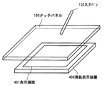
図5に示すように、本発明のタッチパネル100は、液晶表示装置400等の表示装置の表示画面の正面に設けて使用する。導光板101が透光性材料で形成されているため、導光板101を介して表示画面401を見ることができる。表示画面401を見ながらタッチパネル100に入力ペン140により文字や図等を入力すると、入力ペン140の位置変化に合わせて液晶表示装置の画面が変化する。本発明の導光板101は入力ペン140や指先の入力により殆ど変形しないため、下側の液晶表示装置の画面に物理的な力を加えることがない。
As shown in FIG. 5, the touch panel 100 of the present invention is used by being provided in front of a display screen of a display device such as a liquid crystal display device 400. Since the
もちろん、表示装置としては液晶表示装置の他の表示装置でもよく、プラズマディスプレイ、EL(エレクトロルミネッセンス)ディスプレイ等、他の平板型のディスプレイや、CRTでもよい。 Of course, the display device may be another display device of a liquid crystal display device, and may be another flat display such as a plasma display or an EL (electroluminescence) display, or a CRT.
また、本発明のタッチパネルは表示装置と組合せなくとも、タブレットとして用いることもできる。 The touch panel of the present invention can also be used as a tablet without being combined with a display device.
(実施形態4)
実施形態3は液晶表示装置について説明したが、本実施形態では、本発明のタッチパネルと組み合わせて使用されるEL表示装置について説明する。
(Embodiment 4)
Although the liquid crystal display device has been described in Embodiment 3, in this embodiment, an EL display device used in combination with the touch panel of the present invention will be described.
図6(A)はEL表示装置の上面図である。図6(A)において、10は基板、11は画素部、12はソース側駆動回路、13はゲート側駆動回路であり、それぞれの駆動回路は配線14〜16によってFPC17に接続され、外部の回路や電源に接続されている。
FIG. 6A is a top view of the EL display device. In FIG. 6A, 10 is a substrate, 11 is a pixel portion, 12 is a source side driver circuit, 13 is a gate side driver circuit, and each driver circuit is connected to the
画素部を囲むようにして、好ましくは駆動回路及び画素部を囲むようにして、シーリング材(ハウジング材ともいう)18が接着剤19によって基板10に固着されて、基板10との間に密閉空間20が形成されている。このとき、EL素子は完全に前記密閉空間に封入された状態となり、外気から完全に遮断される。
A sealing material (also referred to as a housing material) 18 is fixed to the
さらに、シーリング材18と基板10との間の密閉空間20には不活性ガス(アルゴン、ヘリウム、窒素等)を充填しておいたり、酸化バリウム等の乾燥剤を設けておくことが望ましい。これによりEL素子の水分等による劣化を抑制することが可能である。
Further, it is desirable that the sealed
図6(B)は本実施例のEL表示装置の断面構造であり、基板10、下地膜21の上に駆動回路用TFT(ここではnチャネル型TFTとpチャネル型TFTを組み合わせたCMOS回路を図示している。)22及び画素部用TFT23(ここではEL素子への電流を制御するTFTだけ図示している。)が形成されている。これらのTFTは公知の構造(トップゲート構造またはボトムゲート構造)を用いれば良い。
FIG. 6B shows a cross-sectional structure of the EL display device of this embodiment. A driving circuit TFT (here, a CMOS circuit in which an n-channel TFT and a p-channel TFT are combined) is formed on a
駆動回路用TFT22、画素部用TFT23は樹脂材料でなる層間絶縁膜(平坦化膜)26に覆われている。層間絶縁膜26の上に、画素部用TFT23のドレインと電気的に接続する透明導電膜でなる画素電極27が、形成されている。透明導電膜としては、酸化インジウムと酸化スズとの化合物(ITOと呼ばれる)または酸化インジウムと酸化亜鉛との化合物を用いることができる。画素電極27を覆って絶縁膜28が形成され、絶縁膜28上にEL層29が形成されている。絶縁膜28には画素電極27に対する開口部が形成されている。
The driving circuit TFT 22 and the
EL層29は公知のEL材料(正孔注入層、正孔輸送層、発光層、電子輸送層または電子注入層)を自由に組み合わせて積層構造または単層構造とすればよい。どのような構造とするかは公知の技術を用いればよい。また、EL材料には低分子系材料と高分子系(ポリマー系)材料がある。低分子系材料を用いる場合は蒸着法を用いるが、高分子系材料を用いる場合には、スピンコート法、印刷法またはインクジェット法等の簡易な方法を用いることが可能である。
The
例えば、シャドーマスクを用いて蒸着法によりEL層を形成する。シャドーマスクを用いて画素毎に波長の異なる発光が可能な発光層(赤色発光層、緑色発光層及び青色発光層)を形成することで、カラー表示が可能となる。その他にも、色変換層(CCM)とカラーフィルターを組み合わせた方式、白色発光層とカラーフィルターを組み合わせた方式があるがいずれの方法を用いても良い。勿論、単色発光のEL表示装置とすることもできる。 For example, the EL layer is formed by a vapor deposition method using a shadow mask. Color display is possible by forming a light emitting layer (a red light emitting layer, a green light emitting layer, and a blue light emitting layer) capable of emitting light having different wavelengths for each pixel using a shadow mask. In addition, there are a method in which a color conversion layer (CCM) and a color filter are combined, and a method in which a white light emitting layer and a color filter are combined, but either method may be used. Needless to say, an EL display device emitting monochromatic light can also be used.
EL層29上に陰極30が形成されている。陰極30とEL層29の界面に存在する水分や酸素は極力排除しておくことが望ましい。従って、真空中でEL層29と陰極30を連続成膜するか、EL層29を不活性雰囲気で形成し、大気解放しないで陰極30を形成するといった工夫が必要である。例えば、マルチチャンバー方式(クラスターツール方式)の成膜装置を用いることで上述のような成膜を可能とする。
A
陰極30として、LiF(フッ化リチウム)膜とAl(アルミニウム)膜の積層構造を用いる。具体的にはEL層29上に蒸着法で1nm厚のLiF(フッ化リチウム)膜を形成し、その上に300nm厚のアルミニウム膜を形成する。勿論、公知の陰極材料であるMgAg電極を用いてもよい。
As the
陰極30は31で示される領域において配線16に接続されている。配線16は陰極30に所定の電圧を与えるための電源供給線であり、導電性ペースト材料32を介してFPC17に接続される。
The
31に示された領域において、陰極30と配線16とを電気的に接続するために、層間絶縁膜26及び絶縁膜28にコンタクトホールが形成されている。これらコンタクトホールは層間絶縁膜26のエッチング時(画素電極用コンタクトホールの形成時)や絶縁膜28のエッチング時(EL層形成前の開口部の形成時)に形成しておけば良い。また、絶縁膜28をエッチングする際に、層間絶縁膜26まで一括でエッチングしてもよい。この場合、層間絶縁膜26と絶縁膜28が同じ樹脂材料であれば、コンタクトホールの形状を良好なものとすることができる。
In the region indicated by 31, contact holes are formed in the
配線16はシーリング材18と基板10との間(但し隙間は接着剤19で塞がれている。)を通ってFPC17に電気的に接続されている。なお、配線16と同様に、他の配線14、15もシーリング材18の下を通ってFPC17に電気的に接続されている。
The
(実施形態5)
図7を用いて、本実施形態を説明する。本実施形態は、図5に示した、タッチパネル付きの液晶表示装置を搭載した電子機器に本発明を応用した例である。図7にキーボードレスの情報端末機器を示す。
(Embodiment 5)
This embodiment will be described with reference to FIG. The present embodiment is an example in which the present invention is applied to an electronic apparatus equipped with a liquid crystal display device with a touch panel shown in FIG. FIG. 7 shows a keyboard-less information terminal device.
図7(A)は、wwwブラウズ機能や、電子メール等の通信機能等備えた情報端末機器1000であり、デジタルカメラ1001を搭載し、画面にはタッチパネル付きの液晶表示装置1002を用いている。 FIG. 7A shows an information terminal device 1000 having a www browsing function, a communication function such as an e-mail, and the like, which includes a digital camera 1001 and uses a liquid crystal display device 1002 with a touch panel on the screen.
図7(B)は、通信機能を備えた電子手帳1100であり、画面にはタッチパネル付きの液晶表示装置1102を用いている。 FIG. 7B illustrates an electronic notebook 1100 having a communication function, which uses a liquid crystal display device 1102 with a touch panel on the screen.
本発明のタッチパネルの入力面は導光板でなり、きわめて単純な構造なため、物理的な衝撃に強いので、図7に示すような携帯型の情報端末機器には好適である。 Since the input surface of the touch panel of the present invention is a light guide plate and has a very simple structure, it is resistant to physical impact, and thus is suitable for a portable information terminal device as shown in FIG.
また、本発明は図7に示す情報端末機器だけでなく、従来タッチパネルが用いられていたあらゆる電子機器に応用できる。例えば、券売機、現金自動支払機(ATM)、ファクシミリやコピー機等のOA機器等にも利用できる。 Further, the present invention can be applied not only to the information terminal device shown in FIG. 7 but also to any electronic device that has conventionally used a touch panel. For example, it can be used for ticket machines, cash dispensers (ATM), office automation equipment such as facsimile machines and copiers.
Claims (10)
前記表示画面の正面に重ねて設けられ、透光性材料を有する導光板を備えたタッチパネルを搭載した電子機器であって、
前記表示画面の表示に従って前記タッチパネルに接触し情報を入力するための入力ペンを有し、
前記入力ペンの前記導光板との接触部分は前記導光板を形成する透光性材料の屈折率と同じ又は前記屈折率より大きな屈折率の透光性材料で形成されていることを特徴とする電子機器。 A display screen;
An electronic device equipped with a touch panel provided with a light guide plate having a light-transmitting material provided on the front of the display screen ,
Having an input pen for touching the touch panel and inputting information according to the display on the display screen;
The contact portion of the input pen with the light guide plate is formed of a light transmissive material having a refractive index equal to or greater than the refractive index of the light transmissive material forming the light guide plate. Electronics.
前記表示画面の正面に重ねて設けられ、透光性材料を有する導光板を備えたタッチパネルと、
前記導光板の側面に設けられた光センサーとを搭載した電子機器であって、
前記表示画面の表示に従って前記タッチパネルに接触し情報を入力するための入力ペンを有し、
前記入力ペンの前記導光板との接触部分は前記導光板を形成する透光性材料の屈折率と同じ又は前記屈折率より大きな屈折率の透光性材料で形成されていることを特徴とする電子機器。 A display screen;
Provided to overlap the front of the display screen, a touch panel provided with a light guide plate having a light-transmitting material,
An electronic device equipped with a photosensor provided on a side surface of the light guide plate ,
Having an input pen for touching the touch panel and inputting information according to the display on the display screen;
The contact portion of the input pen with the light guide plate is formed of a light transmissive material having a refractive index equal to or greater than the refractive index of the light transmissive material forming the light guide plate. Electronics.
前記表示画面の正面に重ねて設けられ、透光性材料を有する導光板と、前記導光板の側面に設けられた発光ダイオードと、を備えたタッチパネルと、
前記導光板の他の側面に設けられた光センサーとを搭載した電子機器であって、
前記表示画面の表示に従って前記タッチパネルに接触し情報を入力するための入力ペンを有し、
前記透光性材料は、前記発光ダイオードから照明された光を透過する材料でなり、
前記入力ペンの前記導光板との接触部分は前記導光板を形成する透光性材料の屈折率と同じ又は前記屈折率より大きな屈折率の透光性材料で形成されていることを特徴とする電子機器。 A display screen;
A touch panel comprising a light guide plate provided on the front surface of the display screen and having a light-transmitting material; and a light emitting diode provided on a side surface of the light guide plate ;
An electronic device equipped with a photosensor provided on the other side of the light guide plate ,
Having an input pen for touching the touch panel and inputting information according to the display on the display screen;
The translucent material is a material that transmits light illuminated from the light emitting diode,
The contact portion of the input pen with the light guide plate is formed of a light transmissive material having a refractive index equal to or greater than the refractive index of the light transmissive material forming the light guide plate. Electronics.
前記表示画面の正面に重ねて設けられ、透光性材料を有する導光板と、前記導光板の側面に設けられた発光ダイオードと、前記導光板の側面に設けられ、前記発光ダイオードより前記導光板に近接して設けられたレンズシートと、を備えたタッチパネルと、
前記導光板の他の側面に設けられた光センサーとを搭載した電子機器であって、
前記表示画面の表示に従って前記タッチパネルに接触し情報を入力するための入力ペンを有し、
前記透光性材料は、前記発光ダイオードから照明され、前記レンズシートを通った光を透過する材料でなり、
前記入力ペンの前記導光板との接触部分は前記導光板を形成する透光性材料の屈折率と同じ又は前記屈折率より大きな屈折率の透光性材料で形成されていることを特徴とする電子機器。 A display screen;
A light guide plate provided on the front surface of the display screen and having a translucent material, a light emitting diode provided on a side surface of the light guide plate, and provided on a side surface of the light guide plate, the light guide plate from the light emitting diode. a touch panel and a lens sheet provided close to,
An electronic device equipped with a photosensor provided on the other side of the light guide plate ,
Having an input pen for touching the touch panel and inputting information according to the display on the display screen;
The translucent material is a material that is illuminated from the light emitting diode and transmits light that has passed through the lens sheet ,
The contact portion of the input pen with the light guide plate is formed of a light transmissive material having a refractive index equal to or greater than the refractive index of the light transmissive material forming the light guide plate. Electronics.
前記表示画面の正面に重ねて設けられ、透光性材料を有する導光板を備えたタッチパネルを搭載した電子機器であって、
前記電子機器が有する画面に接触し情報を入力するための入力ペンを有し、
前記入力ペンは、光を吸収する材料を有することを特徴とする電子機器。 A display screen;
An electronic device equipped with a touch panel provided with a light guide plate having a light-transmitting material provided on the front of the display screen ,
Having an input pen for touching the screen of the electronic device and inputting information;
The input pen includes a material that absorbs light.
前記表示画面の正面に重ねて設けられ、透光性材料を有する導光板を備えたタッチパネルと、
前記導光板の側面に設けられた光センサーとを搭載した電子機器であって、
前記表示画面の表示に従って前記タッチパネルに接触し情報を入力するための入力ペンを有し、
前記入力ペンは、光を吸収する材料を有することを特徴とする電子機器。 A display screen;
Provided to overlap the front of the display screen, a touch panel provided with a light guide plate having a light-transmitting material,
An electronic device equipped with a photosensor provided on a side surface of the light guide plate ,
Having an input pen for touching the touch panel and inputting information according to the display on the display screen;
The input pen includes a material that absorbs light.
前記表示画面の正面に重ねて設けられ、透光性材料を有する導光板と、前記導光板の側面に設けられた発光ダイオードと、を備えたタッチパネルと、
前記導光板の他の側面に設けられた光センサーとを搭載した電子機器であって、
前記表示画面の表示に従って前記タッチパネルに接触し情報を入力するための入力ペンを有し、
前記透光性材料は、前記発光ダイオードから照明された光を透過する材料でなり、
前記入力ペンは、光を吸収する材料を有することを特徴とする電子機器。 A display screen;
A touch panel comprising a light guide plate provided on the front surface of the display screen and having a light-transmitting material; and a light emitting diode provided on a side surface of the light guide plate ;
An electronic device equipped with a photosensor provided on the other side of the light guide plate ,
Having an input pen for touching the touch panel and inputting information according to the display on the display screen;
The translucent material is a material that transmits light illuminated from the light emitting diode,
The input pen includes a material that absorbs light.
前記表示画面の正面に重ねて設けられ、透光性材料を有する導光板と、前記導光板の側面に設けられた発光ダイオードと、前記導光板の側面に設けられ、前記発光ダイオードより前記導光板に近接して設けられたレンズシートと、を備えたタッチパネルと、
前記導光板の他の側面に設けられた光センサーとを搭載した電子機器であって、
前記表示画面の表示に従って前記タッチパネルに接触し情報を入力するための入力ペンを有し、
前記透光性材料は、前記発光ダイオードから照明され、前記レンズシートを通った光を透過する材料でなり、
前記入力ペンは、光を吸収する材料を有することを特徴とする電子機器。 A display screen;
A light guide plate provided on the front surface of the display screen and having a translucent material, a light emitting diode provided on a side surface of the light guide plate, and provided on a side surface of the light guide plate, the light guide plate from the light emitting diode. a touch panel and a lens sheet provided close to,
An electronic device equipped with a photosensor provided on the other side of the light guide plate ,
Having an input pen for touching the touch panel and inputting information according to the display on the display screen;
The translucent material is a material that is illuminated from the light emitting diode and transmits light that has passed through the lens sheet ,
The input pen includes a material that absorbs light.
前記レンズシートは、プリズム状又は半円柱状の凸部を複数有することを特徴とする電子機器。 In claim 4 or claim 8 ,
The lens sheet has a plurality of prismatic or semi-cylindrical convex portions.
前記透光性材料は屈折率が1.4〜1.7であることを特徴とする電子機器。 In any one of Claims 1 thru | or 9,
The translucent material has an index of refraction of 1.4 to 1.7.
Priority Applications (1)
| Application Number | Priority Date | Filing Date | Title |
|---|---|---|---|
| JP2006237381A JP4286853B2 (en) | 1998-10-02 | 2006-09-01 | Electronics |
Applications Claiming Priority (2)
| Application Number | Priority Date | Filing Date | Title |
|---|---|---|---|
| JP28150798 | 1998-10-02 | ||
| JP2006237381A JP4286853B2 (en) | 1998-10-02 | 2006-09-01 | Electronics |
Related Parent Applications (1)
| Application Number | Title | Priority Date | Filing Date |
|---|---|---|---|
| JP27329399A Division JP4338845B2 (en) | 1998-10-02 | 1999-09-27 | Touch panel, display device including touch panel, and electronic apparatus including display device |
Publications (2)
| Publication Number | Publication Date |
|---|---|
| JP2006318512A JP2006318512A (en) | 2006-11-24 |
| JP4286853B2 true JP4286853B2 (en) | 2009-07-01 |
Family
ID=37539060
Family Applications (1)
| Application Number | Title | Priority Date | Filing Date |
|---|---|---|---|
| JP2006237381A Expired - Fee Related JP4286853B2 (en) | 1998-10-02 | 2006-09-01 | Electronics |
Country Status (1)
| Country | Link |
|---|---|
| JP (1) | JP4286853B2 (en) |
Families Citing this family (12)
| Publication number | Priority date | Publication date | Assignee | Title |
|---|---|---|---|---|
| US8144271B2 (en) | 2006-08-03 | 2012-03-27 | Perceptive Pixel Inc. | Multi-touch sensing through frustrated total internal reflection |
| US8441467B2 (en) | 2006-08-03 | 2013-05-14 | Perceptive Pixel Inc. | Multi-touch sensing display through frustrated total internal reflection |
| WO2009018317A2 (en) * | 2007-07-30 | 2009-02-05 | Perceptive Pixel, Inc. | Liquid multi-touch sensor and display device |
| JP5368731B2 (en) * | 2007-09-19 | 2013-12-18 | キヤノン株式会社 | Touch panel |
| US8736581B2 (en) | 2009-06-01 | 2014-05-27 | Perceptive Pixel Inc. | Touch sensing with frustrated total internal reflection |
| US8624853B2 (en) | 2009-06-01 | 2014-01-07 | Perceptive Pixel Inc. | Structure-augmented touch sensing with frustated total internal reflection |
| WO2010141453A2 (en) | 2009-06-01 | 2010-12-09 | Han Jefferson Y | Touch sensing |
| CN101847063B (en) * | 2010-03-03 | 2013-04-17 | 苏州佳世达电通有限公司 | System and method for detecting object by using non-coincident fields of light |
| CN101923418B (en) * | 2010-03-07 | 2013-01-16 | 苏州佳世达电通有限公司 | Object sensing system and method |
| KR101749266B1 (en) * | 2010-03-24 | 2017-07-04 | 삼성디스플레이 주식회사 | Touch sensing display device and cumputer-readable medium |
| FR3025052B1 (en) * | 2014-08-19 | 2017-12-15 | Isorg | DEVICE FOR DETECTING ELECTROMAGNETIC RADIATION IN ORGANIC MATERIALS |
| KR101536759B1 (en) * | 2014-11-13 | 2015-07-15 | 주식회사 엣지아이앤디 | Touch Pen With Light Absorption Unit |
Family Cites Families (6)
| Publication number | Priority date | Publication date | Assignee | Title |
|---|---|---|---|---|
| JPH0367319A (en) * | 1989-08-04 | 1991-03-22 | Fujitsu Ltd | Optical coordinate input device |
| JPH0580935A (en) * | 1991-03-25 | 1993-04-02 | Minato Electron Kk | Optical touch panel with optical distributor |
| JPH1027067A (en) * | 1996-07-10 | 1998-01-27 | Fujitsu General Ltd | Coordinate recognition system |
| JPH1091348A (en) * | 1996-09-19 | 1998-04-10 | Toshiba Corp | Coordinate input device and liquid crystal display device |
| JP4097752B2 (en) * | 1997-10-14 | 2008-06-11 | Dowaホールディングス株式会社 | Optical input device |
| JP2002259347A (en) * | 2001-03-02 | 2002-09-13 | Seiko Epson Corp | Wristwatch-type information processing apparatus, screen display method, program, and recording medium |
-
2006
- 2006-09-01 JP JP2006237381A patent/JP4286853B2/en not_active Expired - Fee Related
Also Published As
| Publication number | Publication date |
|---|---|
| JP2006318512A (en) | 2006-11-24 |
Similar Documents
| Publication | Publication Date | Title |
|---|---|---|
| JP5238475B2 (en) | Display device provided with touch panel, and electronic device | |
| JP4338845B2 (en) | Touch panel, display device including touch panel, and electronic apparatus including display device | |
| JP4286853B2 (en) | Electronics | |
| US11800746B2 (en) | Electronic devices with light sensors and displays | |
| JP4891666B2 (en) | Liquid crystal display | |
| US6597348B1 (en) | Information-processing device | |
| EP1668483A2 (en) | Light guide touch screen | |
| CN1856766A (en) | Coordinate detection system for a display monitor | |
| US8350829B2 (en) | Input pen for touch-panel and touch-panel input system | |
| WO2018103193A1 (en) | Display module and usage method thereof | |
| WO2018188670A1 (en) | Detection apparatus and terminal device | |
| TWI410685B (en) | Light guide module, optical touch module, and method of increasing signal to noise ratio of optical touch module | |
| CN110598663B (en) | Display screen assembly, electronic equipment and fingerprint processing method | |
| JP4493774B2 (en) | Electronics | |
| JP2010026693A (en) | Information input device, image display, and stylus pen | |
| CN100421057C (en) | light pen | |
| JP4515444B2 (en) | Display device | |
| TWI798724B (en) | Electronic device with high-transparency display module | |
| JPH0658272B2 (en) | Tactile sensor | |
| WO2010038510A1 (en) | Display device and touch panel | |
| CN118613115A (en) | Display panel and display device |
Legal Events
| Date | Code | Title | Description |
|---|---|---|---|
| A621 | Written request for application examination |
Free format text: JAPANESE INTERMEDIATE CODE: A621 Effective date: 20060901 |
|
| A131 | Notification of reasons for refusal |
Free format text: JAPANESE INTERMEDIATE CODE: A131 Effective date: 20080819 |
|
| A521 | Written amendment |
Free format text: JAPANESE INTERMEDIATE CODE: A523 Effective date: 20080826 |
|
| A131 | Notification of reasons for refusal |
Free format text: JAPANESE INTERMEDIATE CODE: A131 Effective date: 20090106 |
|
| A521 | Written amendment |
Free format text: JAPANESE INTERMEDIATE CODE: A523 Effective date: 20090227 |
|
| TRDD | Decision of grant or rejection written | ||
| A01 | Written decision to grant a patent or to grant a registration (utility model) |
Free format text: JAPANESE INTERMEDIATE CODE: A01 Effective date: 20090324 |
|
| A01 | Written decision to grant a patent or to grant a registration (utility model) |
Free format text: JAPANESE INTERMEDIATE CODE: A01 |
|
| A61 | First payment of annual fees (during grant procedure) |
Free format text: JAPANESE INTERMEDIATE CODE: A61 Effective date: 20090325 |
|
| FPAY | Renewal fee payment (event date is renewal date of database) |
Free format text: PAYMENT UNTIL: 20120403 Year of fee payment: 3 |
|
| R150 | Certificate of patent or registration of utility model |
Free format text: JAPANESE INTERMEDIATE CODE: R150 |
|
| FPAY | Renewal fee payment (event date is renewal date of database) |
Free format text: PAYMENT UNTIL: 20120403 Year of fee payment: 3 |
|
| FPAY | Renewal fee payment (event date is renewal date of database) |
Free format text: PAYMENT UNTIL: 20120403 Year of fee payment: 3 |
|
| FPAY | Renewal fee payment (event date is renewal date of database) |
Free format text: PAYMENT UNTIL: 20130403 Year of fee payment: 4 |
|
| FPAY | Renewal fee payment (event date is renewal date of database) |
Free format text: PAYMENT UNTIL: 20130403 Year of fee payment: 4 |
|
| FPAY | Renewal fee payment (event date is renewal date of database) |
Free format text: PAYMENT UNTIL: 20140403 Year of fee payment: 5 |
|
| R250 | Receipt of annual fees |
Free format text: JAPANESE INTERMEDIATE CODE: R250 |
|
| R250 | Receipt of annual fees |
Free format text: JAPANESE INTERMEDIATE CODE: R250 |
|
| R250 | Receipt of annual fees |
Free format text: JAPANESE INTERMEDIATE CODE: R250 |
|
| R250 | Receipt of annual fees |
Free format text: JAPANESE INTERMEDIATE CODE: R250 |
|
| LAPS | Cancellation because of no payment of annual fees |