JP4282612B2 - Memory device and refresh method thereof - Google Patents
Memory device and refresh method thereof Download PDFInfo
- Publication number
- JP4282612B2 JP4282612B2 JP2005011626A JP2005011626A JP4282612B2 JP 4282612 B2 JP4282612 B2 JP 4282612B2 JP 2005011626 A JP2005011626 A JP 2005011626A JP 2005011626 A JP2005011626 A JP 2005011626A JP 4282612 B2 JP4282612 B2 JP 4282612B2
- Authority
- JP
- Japan
- Prior art keywords
- state
- cell
- data
- memory cell
- refresh
- Prior art date
- Legal status (The legal status is an assumption and is not a legal conclusion. Google has not performed a legal analysis and makes no representation as to the accuracy of the status listed.)
- Expired - Fee Related
Links
- 238000000034 method Methods 0.000 title claims description 23
- 230000015654 memory Effects 0.000 claims description 99
- 238000012544 monitoring process Methods 0.000 claims description 5
- 239000012782 phase change material Substances 0.000 claims 3
- 230000014759 maintenance of location Effects 0.000 description 14
- 238000010586 diagram Methods 0.000 description 9
- 238000009826 distribution Methods 0.000 description 6
- 230000000694 effects Effects 0.000 description 4
- 230000020169 heat generation Effects 0.000 description 2
- 229910052751 metal Inorganic materials 0.000 description 2
- 239000002184 metal Substances 0.000 description 2
- 238000012986 modification Methods 0.000 description 2
- 230000004048 modification Effects 0.000 description 2
- 238000012545 processing Methods 0.000 description 2
- 239000007784 solid electrolyte Substances 0.000 description 2
- BQCADISMDOOEFD-UHFFFAOYSA-N Silver Chemical compound [Ag] BQCADISMDOOEFD-UHFFFAOYSA-N 0.000 description 1
- 150000004770 chalcogenides Chemical class 0.000 description 1
- 238000001816 cooling Methods 0.000 description 1
- 239000013078 crystal Substances 0.000 description 1
- 238000002425 crystallisation Methods 0.000 description 1
- 230000008025 crystallization Effects 0.000 description 1
- 230000003111 delayed effect Effects 0.000 description 1
- 230000006870 function Effects 0.000 description 1
- 150000002500 ions Chemical class 0.000 description 1
- 239000000463 material Substances 0.000 description 1
- 239000011159 matrix material Substances 0.000 description 1
- 238000004904 shortening Methods 0.000 description 1
- 229910052709 silver Inorganic materials 0.000 description 1
- 239000004332 silver Substances 0.000 description 1
Images


Classifications
-
- G—PHYSICS
- G11—INFORMATION STORAGE
- G11C—STATIC STORES
- G11C13/00—Digital stores characterised by the use of storage elements not covered by groups G11C11/00, G11C23/00, or G11C25/00
- G11C13/0002—Digital stores characterised by the use of storage elements not covered by groups G11C11/00, G11C23/00, or G11C25/00 using resistive RAM [RRAM] elements
- G11C13/0021—Auxiliary circuits
- G11C13/0069—Writing or programming circuits or methods
-
- G—PHYSICS
- G11—INFORMATION STORAGE
- G11C—STATIC STORES
- G11C11/00—Digital stores characterised by the use of particular electric or magnetic storage elements; Storage elements therefor
- G11C11/21—Digital stores characterised by the use of particular electric or magnetic storage elements; Storage elements therefor using electric elements
- G11C11/34—Digital stores characterised by the use of particular electric or magnetic storage elements; Storage elements therefor using electric elements using semiconductor devices
- G11C11/40—Digital stores characterised by the use of particular electric or magnetic storage elements; Storage elements therefor using electric elements using semiconductor devices using transistors
- G11C11/401—Digital stores characterised by the use of particular electric or magnetic storage elements; Storage elements therefor using electric elements using semiconductor devices using transistors forming cells needing refreshing or charge regeneration, i.e. dynamic cells
- G11C11/406—Management or control of the refreshing or charge-regeneration cycles
-
- G—PHYSICS
- G11—INFORMATION STORAGE
- G11C—STATIC STORES
- G11C11/00—Digital stores characterised by the use of particular electric or magnetic storage elements; Storage elements therefor
- G11C11/21—Digital stores characterised by the use of particular electric or magnetic storage elements; Storage elements therefor using electric elements
- G11C11/34—Digital stores characterised by the use of particular electric or magnetic storage elements; Storage elements therefor using electric elements using semiconductor devices
- G11C11/40—Digital stores characterised by the use of particular electric or magnetic storage elements; Storage elements therefor using electric elements using semiconductor devices using transistors
- G11C11/401—Digital stores characterised by the use of particular electric or magnetic storage elements; Storage elements therefor using electric elements using semiconductor devices using transistors forming cells needing refreshing or charge regeneration, i.e. dynamic cells
- G11C11/4063—Auxiliary circuits, e.g. for addressing, decoding, driving, writing, sensing or timing
- G11C11/407—Auxiliary circuits, e.g. for addressing, decoding, driving, writing, sensing or timing for memory cells of the field-effect type
- G11C11/409—Read-write [R-W] circuits
- G11C11/4099—Dummy cell treatment; Reference voltage generators
-
- G—PHYSICS
- G11—INFORMATION STORAGE
- G11C—STATIC STORES
- G11C11/00—Digital stores characterised by the use of particular electric or magnetic storage elements; Storage elements therefor
- G11C11/56—Digital stores characterised by the use of particular electric or magnetic storage elements; Storage elements therefor using storage elements with more than two stable states represented by steps, e.g. of voltage, current, phase, frequency
- G11C11/5678—Digital stores characterised by the use of particular electric or magnetic storage elements; Storage elements therefor using storage elements with more than two stable states represented by steps, e.g. of voltage, current, phase, frequency using amorphous/crystalline phase transition storage elements
-
- G—PHYSICS
- G11—INFORMATION STORAGE
- G11C—STATIC STORES
- G11C13/00—Digital stores characterised by the use of storage elements not covered by groups G11C11/00, G11C23/00, or G11C25/00
- G11C13/0002—Digital stores characterised by the use of storage elements not covered by groups G11C11/00, G11C23/00, or G11C25/00 using resistive RAM [RRAM] elements
- G11C13/0004—Digital stores characterised by the use of storage elements not covered by groups G11C11/00, G11C23/00, or G11C25/00 using resistive RAM [RRAM] elements comprising amorphous/crystalline phase transition cells
-
- G—PHYSICS
- G11—INFORMATION STORAGE
- G11C—STATIC STORES
- G11C13/00—Digital stores characterised by the use of storage elements not covered by groups G11C11/00, G11C23/00, or G11C25/00
- G11C13/0002—Digital stores characterised by the use of storage elements not covered by groups G11C11/00, G11C23/00, or G11C25/00 using resistive RAM [RRAM] elements
- G11C13/0021—Auxiliary circuits
- G11C13/0033—Disturbance prevention or evaluation; Refreshing of disturbed memory data
-
- G—PHYSICS
- G11—INFORMATION STORAGE
- G11C—STATIC STORES
- G11C13/00—Digital stores characterised by the use of storage elements not covered by groups G11C11/00, G11C23/00, or G11C25/00
- G11C13/0002—Digital stores characterised by the use of storage elements not covered by groups G11C11/00, G11C23/00, or G11C25/00 using resistive RAM [RRAM] elements
- G11C13/0021—Auxiliary circuits
- G11C13/0064—Verifying circuits or methods
-
- G—PHYSICS
- G11—INFORMATION STORAGE
- G11C—STATIC STORES
- G11C16/00—Erasable programmable read-only memories
- G11C16/02—Erasable programmable read-only memories electrically programmable
- G11C16/06—Auxiliary circuits, e.g. for writing into memory
- G11C16/34—Determination of programming status, e.g. threshold voltage, overprogramming or underprogramming, retention
- G11C16/3418—Disturbance prevention or evaluation; Refreshing of disturbed memory data
- G11C16/3431—Circuits or methods to detect disturbed nonvolatile memory cells, e.g. which still read as programmed but with threshold less than the program verify threshold or read as erased but with threshold greater than the erase verify threshold, and to reverse the disturbance via a refreshing programming or erasing step
-
- G—PHYSICS
- G11—INFORMATION STORAGE
- G11C—STATIC STORES
- G11C16/00—Erasable programmable read-only memories
- G11C16/02—Erasable programmable read-only memories electrically programmable
- G11C16/06—Auxiliary circuits, e.g. for writing into memory
- G11C16/34—Determination of programming status, e.g. threshold voltage, overprogramming or underprogramming, retention
- G11C16/349—Arrangements for evaluating degradation, retention or wearout, e.g. by counting erase cycles
-
- G—PHYSICS
- G11—INFORMATION STORAGE
- G11C—STATIC STORES
- G11C2211/00—Indexing scheme relating to digital stores characterized by the use of particular electric or magnetic storage elements; Storage elements therefor
- G11C2211/401—Indexing scheme relating to cells needing refreshing or charge regeneration, i.e. dynamic cells
- G11C2211/406—Refreshing of dynamic cells
- G11C2211/4061—Calibration or ate or cycle tuning
Landscapes
- Engineering & Computer Science (AREA)
- Computer Hardware Design (AREA)
- Microelectronics & Electronic Packaging (AREA)
- Chemical & Material Sciences (AREA)
- Crystallography & Structural Chemistry (AREA)
- Semiconductor Memories (AREA)
- Dram (AREA)
Description
本発明は、プログラム可能な抵抗素子付き(相変化)メモリとそのリフレッシュ方法に関する。 The present invention relates to a programmable resistive element (phase change) memory and a refresh method thereof.
プログラム可能な抵抗素子付きメモリの一例として、相変化メモリは、例えばカルコゲナイド系の材料(Ge,Sb,Te)に熱を加えることにより、アモルファス状態(高抵抗)/結晶状態(低抵抗)になる性質を利用した不揮発性メモリである。一般には、電流により発生するジュール熱と印加時間により、高抵抗(Reset)/低抵抗(Set)状態に変化をさせる。 As an example of a memory with a programmable resistance element, a phase change memory is in an amorphous state (high resistance) / crystalline state (low resistance) by applying heat to, for example, a chalcogenide-based material (Ge, Sb, Te). This is a non-volatile memory utilizing the properties. In general, the state is changed to a high resistance (Reset) / low resistance (Set) state by Joule heat generated by current and application time.
相変化メモリにおいて、書込み時間は、数10〜100ns程度の時間が必要とされている。また、繰り返し書込み回数は1012回程度と、FLASHメモリ(電気的にプログラム可能、消去可能な不揮発性メモリ)と同程度であり、DRAM(ダイナミックランダムアクセスメモリ)のそれと比較すると4桁程度低い。 In the phase change memory, a write time of about several tens to 100 ns is required. Further, the repeating number of writes is about 10 12 times, (available electrically programmable, non-volatile memory erasable) FLASH memory is about the same, DRAM 4 orders of magnitude when compared with that of (dynamic random access memories) low.
そして、相変化メモリは、読み出し・書込みの繰り返しを重ねるたびに、素子特性の悪化が発生し記憶データが破壊される可能性がある。 In the phase change memory, every time reading and writing are repeated, there is a possibility that the device characteristics deteriorate and the stored data is destroyed.
上記のようなプログラム可能な抵抗素子付きメモリのディスターブ、リテンション特性を向上させる方法として、特許文献1(US6646902B2)や特許文献2(US6560155B1)などにいくつかの提案がなされている。特許文献1(US6646902B2)で開示される例を、図11を参照して簡単に説明行う。本件で採用されるプログラム可能な抵抗素子としては、上部電極1101と下部電極1102との間に例えば銀(Ag)を含んだ固体電界質1103をはさんだ構造をとる。電極間に電位を与えると、イオン化されたAg+イオンが電子と結合し、Ag金属となって析出し、上部電極1101と下部電極1102とを接続して低抵抗状態とし、また、電極1101、1102間に逆の電位を与えると、析出したAg金属を消滅させ高抵抗状態を作り出す方法により、電極間の抵抗値を可変にすることができる。
As a method for improving the disturb and retention characteristics of the memory with a programmable resistance element as described above, several proposals have been made in Patent Document 1 (US 6646902B2), Patent Document 2 (US 6560155B1), and the like. An example disclosed in Patent Document 1 (US Pat. No. 6,646,902 B2) will be briefly described with reference to FIG. The programmable resistance element employed in this case has a structure in which a
図11の構成によれば、このプログラム状態を保持可能な時間は時間もしくは日単位程度であり、DRAMに比較すれば、保持時間は長いものの、FLASHメモリなど一般の不揮発性メモリと比較すると、リテンションは劣っている。そのため、プログラム時の電圧V1に対し、ディスターブを与えない程度の電圧V2(V1のおよそ35%〜60%)を与え、リテンション特性の向上を図るという提案がなされている。 According to the configuration of FIG. 11, the time during which the program state can be held is about hours or days, and the retention time is longer than that of a DRAM, but the retention time is longer than that of a general nonvolatile memory such as a FLASH memory. Is inferior. Therefore, a proposal has been made to improve the retention characteristics by applying a voltage V2 (approximately 35% to 60% of V1) that does not disturb the voltage V1 at the time of programming.
また、特許文献2(US6560155B1)においては、特許文献1(US6646902B2)に示されたものと同様のメモリセルを用いたDRAMインターフェース互換のメモリの提供を実現するため、リフレッシュ動作を行う提案がなされている。 In Patent Document 2 (US Pat. No. 6,560,155 B1), in order to provide a DRAM interface compatible memory using memory cells similar to those disclosed in Patent Document 1 (US Pat. No. 6,646,902 B2), a proposal for performing a refresh operation has been made. Yes.
前述のプログラム可能な抵抗素子付きメモリセルのリテンション特性は、DRAMより優れていることより、DRAMの内部リフレッシュタイミングを遅延回路にて遅延させ、定期的に電圧を加えることにより、リテンション特性の向上を図るとともに、リフレッシュ電流・パワーの削減を図るという提案がなされている。 The above-mentioned retention characteristic of the memory cell with a programmable resistive element is superior to that of the DRAM. Therefore, the internal refresh timing of the DRAM is delayed by a delay circuit, and the voltage is periodically applied to improve the retention characteristic. At the same time, proposals have been made to reduce the refresh current and power.
相変化素子は、不揮発性メモリ素子ではあるが、リードディスターブにより、相変化素子に電圧・電流が加わることにより、相変化素子の抵抗値の変化が起こり、リテンション特性と読み出しマージンを悪化させる。 Although the phase change element is a non-volatile memory element, a voltage / current is applied to the phase change element due to read disturb, thereby causing a change in the resistance value of the phase change element, which deteriorates the retention characteristic and the read margin.
また同様にして、ライト時においても、同様のディスターブにより相変化素子に電圧・電流が加わることにより、その抵抗値の変化が時間とともに劣化していくことが知られている(図9)。図9は、書込み・読み出しでの相変化素子の抵抗値の変化を示す図であり、横軸は読出し/書き込み回数、縦軸は相変化素子のSet/Resetの抵抗値である。 Similarly, during writing, it is known that a change in resistance value deteriorates with time by applying a voltage / current to the phase change element due to the same disturbance (FIG. 9). FIG. 9 is a diagram illustrating changes in the resistance value of the phase change element during writing / reading, in which the horizontal axis represents the number of read / write operations, and the vertical axis represents the Set / Reset resistance value of the phase change element.
相変化素子を用いDRAMインターフェース互換のメモリ製品を実現する上で以下のような課題を有している。 In order to realize a DRAM interface compatible memory product using a phase change element, it has the following problems.
1)繰り返し書込み回数は、1012回程度とFLASHメモリと同程度であり、DRAMのそれと比較すると、4桁程度低い。読み出し・書込みの繰り返しを重ねるたびに、素子特性の悪化が発生し、記憶データが破壊されることもある(前述した図9参照)。 1) repeat number of writes is about the same as the FLASH memory 10 12 times, when compared to that of DRAM, 4 orders of magnitude lower. Each time reading / writing is repeated, the device characteristics deteriorate, and the stored data may be destroyed (see FIG. 9 described above).
2)同一データを繰り返し同一セルに書込みを行った場合、例えば、低抵抗状態がより深く低抵抗状態になり、高抵抗状態に書込みを行ったにもかかわらず、高抵抗になりきらないなどの問題が発生する(図9参照)。図10は、書込み・読み出しでの従来の相変化素子の抵抗値の変化・分布を示す図であり、初期Reset抵抗分布(RReset)とn回書き換え後のReset抵抗分布(Rreset’)、初期Set抵抗分布(RSset)とn回書き換え後のSet抵抗分布(RSet’)が示されている。 2) When the same data is repeatedly written to the same cell, for example, the low resistance state becomes deeper and lower resistance state, and the resistance does not become high even though writing is performed in the high resistance state. A problem occurs (see FIG. 9). FIG. 10 is a diagram showing changes and distributions of resistance values of a conventional phase change element in writing / reading. The initial Reset resistance distribution (RReset), the Reset resistance distribution after rewriting n times (Rreset '), and the initial Set. A resistance distribution (RSset) and a Set resistance distribution (RSet ′) after n rewrites are shown.
データを上書きする場合においては、その素子の特性から状態の変化が発生し、抵抗値が変動するため、メモリセル間の抵抗ばらつきが大きくなり、特性に大きな影響を及ぼす(図9、図10参照)などが考えられ、単純に読み出し/書込みを繰り返すと、相変化素子の上記の特性から、リテンション特性の悪化を引き起こし、メモリ素子としての機能を果たさなくなる、という問題点がある。 When data is overwritten, a change in state occurs due to the characteristics of the element and the resistance value fluctuates, so that the resistance variation between memory cells increases, greatly affecting the characteristics (see FIGS. 9 and 10). If the read / write operation is simply repeated, there is a problem that the retention characteristic is deteriorated due to the above characteristics of the phase change element, and the function as the memory element is not performed.
したがって、本発明は、上記問題点に鑑みて創案されたものであって、その目的は、相変化素子のリテンション特性の改善を図るメモリ装置及びそのリフレッシュ方法を提供することにある。 Accordingly, the present invention has been made in view of the above problems, and an object of the present invention is to provide a memory device and a refresh method thereof for improving the retention characteristics of a phase change element.
本願で開示される発明は、上記問題点を解決するため、概略以下の構成とされる。 The invention disclosed in the present application is generally configured as follows in order to solve the above problems.
本発明の相変化メモリは、DRAMインターフェース互換のメモリであることを利用し、読み出し・書込み回数に応じたストレスが与えられる基準セルを設け、該基準セルの相変化素子の抵抗値の変化を検出し、予め設定した基準値以上に抵抗値が変化していた場合(低抵抗化)、内部回路に対してリフレッシュ動作を要求し、メモリセルおよび基準セルを、一旦、リフレッシュする。かかる構成により、相変化素子のプログラム抵抗値のばらつきを補正し、マージン確保と同時にリテンション特性の改善を図るものである。 The phase change memory of the present invention uses a DRAM interface compatible memory, and provides a reference cell to which stress is applied according to the number of reading / writing, and detects a change in resistance value of the phase change element of the reference cell. If the resistance value has changed more than a preset reference value (lower resistance), the internal circuit is requested to perform a refresh operation, and the memory cell and the reference cell are once refreshed. With such a configuration, variation in the program resistance value of the phase change element is corrected, and a retention characteristic is improved simultaneously with securing a margin.
本発明の1つのアスペクト(側面)に係る装置は、ビット線とワード線の交差部に、プログラム可能な抵抗素子を含むメモリセルを備え、前記メモリセルの抵抗値の変化に応じて、前記メモリセルのリフレッシュ動作を行うように制御する制御回路を備えている。 An apparatus according to one aspect of the present invention includes a memory cell including a programmable resistance element at an intersection of a bit line and a word line, and the memory according to a change in a resistance value of the memory cell. A control circuit is provided for controlling the cell refresh operation.
本発明に係るメモリ装置において、読み出し・書込み回数に応じたストレスが与えられるダミーセルの相変化素子の抵抗値の変化を検出し、前記ダミーセルの相変化素子が予め設定された基準値以上に抵抗値が変化していた場合に、内部回路に対して、リフレッシュ要求を行い、前記リフレッシュ要求に基づき、メモリセルおよびダミーセルをリフレッシュする構成としてもよい。 In the memory device according to the present invention, a change in the resistance value of the phase change element of the dummy cell to which stress is applied according to the number of times of reading and writing is detected, and the resistance value of the dummy cell phase change element exceeds a preset reference value. When the change has occurred, a refresh request may be made to the internal circuit, and the memory cell and the dummy cell may be refreshed based on the refresh request.
本発明に係るメモリ装置は、別のアスペクトにおいて、相変化素子を備えたメモリセルの読み出し回数をカウントし、読み出し回数をモニタして所定回数に達した時に、内部回路にリフレッシュ要求する構成としてもよい。 In another aspect, the memory device according to the present invention may be configured to count the number of readings of the memory cell including the phase change element, and monitor the number of readings to request a refresh from the internal circuit when the number reaches a predetermined number. Good.
本発明に係るメモリ装置は、さらに別のアスペクトにおいて、相変化素子を備えたメモリの第1の状態と第2の状態にそれぞれ対応する第1、第2の基準電流と、前記メモリセルを流れる電流とを比較し、前記メモリセルを流れる電流に所望のずれが発生した場合に、内部回路に対して、リフレッシュを要求し、リフレッシュ要求に基づき、メモリセルをリフレッシュする構成としてもよい。 According to another aspect of the memory device of the present invention, first and second reference currents respectively corresponding to a first state and a second state of a memory including a phase change element, and the memory cell flow. The current may be compared, and when a desired deviation occurs in the current flowing through the memory cell, the internal circuit may be requested to refresh, and the memory cell may be refreshed based on the refresh request.
本発明の一のアスペクト(側面)に係る方法は、読み出し・書込み回数に応じたストレスが与えられるダミーセルの相変化素子の抵抗値の変化を検出する工程と、
前記ダミーセルの相変化素子が予め設定された基準値以上に抵抗値が変化していた場合に、内部回路に対して、リフレッシュ要求を行う工程と、
前記リフレッシュ要求に基づき、メモリセルおよびダミーセルをリフレッシュする工程と、を含む。
A method according to one aspect of the present invention includes a step of detecting a change in resistance value of a phase change element of a dummy cell to which stress is applied according to the number of times of reading and writing;
A step of making a refresh request to the internal circuit when the resistance value of the phase change element of the dummy cell has changed more than a preset reference value;
Refreshing the memory cell and the dummy cell based on the refresh request.
本発明によれば、相変化素子のプログラム抵抗値のばらつきを補正し、マージン確保と同時にリテンション特性の改善を図ることができる。 According to the present invention, it is possible to correct the variation in the program resistance value of the phase change element, and to secure the margin and simultaneously improve the retention characteristic.
本発明の実施の形態について説明する。本発明の一実施の形態のメモリ装置は、相変化メモリの読み出し・書込み回数に応じたストレスを与えられる基準セルを設け、その基準セルの相変化素子抵抗値の変化を検出し、設定した基準値以上に抵抗値が変化していた場合(低抵抗化)、内部回路にリフレッシュ動作を要求する手段を備えることで、データ・リテンション特性の向上を図る。 Embodiments of the present invention will be described. A memory device according to an embodiment of the present invention includes a reference cell that can be stressed according to the number of reads / writes of a phase change memory, detects a change in the phase change element resistance value of the reference cell, and sets a reference If the resistance value has changed more than the value (lower resistance), the data retention characteristics are improved by providing means for requesting a refresh operation in the internal circuit.
本発明の実施の形態について説明する。図1は、本発明の実施の形態のメモリの構成を示す図である。図1を参照すると、本発明の一実施の形態に係るメモリは、メモリセル101と、メモリセル101に書き込まれたデータをセンス増幅するセンスアンプ102と、メモリセル101にデータを書き込むためのライトアンプ103と、データ退避用のデータレジスタ105と、リフレッシュ時にメモリセルのデータの書込み状態を比較・検出するベリファイ(Verify)用アンプ104と、セット(Set)抵抗をプログラムされたSetダミーセル109と、リセット(Reset)抵抗をプログラムされたResetダミーセル110と、Setダミーセル109の抵抗値を監視するSet比較回路111と、Resetダミーセル110の抵抗値を監視するReset比較回路112と、Set比較回路111とReset比較回路112での比較結果からリフレッシュ要求の有無を判断し、内部にリフレッシュ要求を行うリフレッシュ要求回路107と、プログラム・ベリファイ時のライト・パルスを制御するライトパルス制御化回路106と、ダミーセルに対しても、リフレッシュ動作時においては、同時に書込みを行うためのダミーセルライトアンプ108とを備えている。
Embodiments of the present invention will be described. FIG. 1 is a diagram showing a configuration of a memory according to an embodiment of the present invention. Referring to FIG. 1, a memory according to an embodiment of the present invention includes a
図2は、メモリセル部及びダミーセル、センスアンプ及びライトアンプの回路構成を示す図である。 FIG. 2 is a diagram illustrating a circuit configuration of the memory cell unit, the dummy cell, the sense amplifier, and the write amplifier.
図2を参照すると、複数のメモリセル101が、X/Yのマトリクス状に配置されており、それぞれのメモリセルトランジスタのソースとBit線の間に、模式的に抵抗素子として示されている相変化素子を備えている。
Referring to FIG. 2, a plurality of
相変化素子は、高電圧(高電流)+ショートパルスを印加し、ジュール熱による発熱と急冷により、相変化素子は、アモルファス化し、高抵抗化(「Reset」という)となる。また、前記より低い電流で長いパルスにより、ある程度の時間暖めることにより、相変化素子は結晶化し、低抵抗化(「Set」という)する。 The phase change element is applied with a high voltage (high current) + short pulse, and the phase change element becomes amorphous due to heat generation and rapid cooling due to Joule heat, resulting in a high resistance (referred to as “Reset”). In addition, the phase change element is crystallized and lowered in resistance (referred to as “Set”) by being warmed for a certain period of time by a long pulse at a lower current.
このように、相変化素子を、アモルファス/結晶状態を変化させ、その抵抗値の変化により、プログラムを行っている。 As described above, the phase change element is programmed by changing the amorphous / crystalline state and changing the resistance value.
一方、Setダミーセル109、Resetダミーセル110は、Set/Reset状態にメモリセルと同様に書込みを行う。メモリセル領域に配置し、ワード線はメモリセルと共通とし、また、ビット(Bit)線には、メモリセルの選択時にかかる電流ストレスが加わるように、図3、図4のバイアス回路302、402を備えている。
On the other hand, the
メモリセルと同様に選択されたワード線につながれたダミーセルが選択状態となり、読み出し・書込みストレスが加わると同時に、非選択セルについても、Bit線に付く容量による充放電による微小なストレスがかかる。これらを、選択セルにおけるディスターブ・非選択セルにおけるディスターブという。 Similar to the memory cell, the dummy cell connected to the selected word line is selected and read / write stress is applied. At the same time, the non-selected cell is also subjected to minute stress due to charge / discharge due to the capacitance attached to the bit line. These are referred to as disturb in the selected cell and disturb in the non-selected cell.
図3及び図4に、ダミーセルの抵抗値をモニターするための比較回路の構成を示す。より詳細には、図3は、Setダミーセルの抵抗をモニタするためのSet比較回路111の構成を示すであり、図4は、Resetダミーセルの抵抗をモニタするためのReset比較回路112の構成を示す図である。
3 and 4 show the configuration of a comparison circuit for monitoring the resistance value of the dummy cell. More specifically, FIG. 3 shows the configuration of the
ここで、iSet、及びiResetは、それぞれ定電流源303、403から所望の電流値を設定する。例えば、この定電流は、Setセル301に書き込むべき抵抗値を、相変化素子以外の抵抗素子を設け、基準抵抗として、バイアス手段により、定電流源を実現する手段がある。
Here, iSet and iReset set desired current values from the constant
基準抵抗と、書込み抵抗値(Setダミーセル、メモリセル)とを同一となるようにし、バイアス手段も同一とした場合について考える。 Consider a case where the reference resistance and the write resistance value (Set dummy cell, memory cell) are made the same, and the bias means is also made the same.
図3において、iSetなる電流を、基準電流とした場合、定電流源303に接続するNMOSトランジスタN10にも、基準電流iSetなる電流が流れる。NMOSトランジスタN10とN11は、カレントミラー回路を構成しており、このため、NMOSトランジスタN11にも、がミラー電流として電流iSet流れる。
In FIG. 3, when the current iSet is a reference current, the current ISet also flows through the NMOS transistor N 10 connected to the constant
一方、Setダミーセル(SetCell)につながるバイアス(Bias)回路302にて、Setダミーセル109に電流が供給がなされ、バイアス回路302とPMOSトランジスタP11とがカレントミラーを構成すると、このPMOSトランジスタP11には、iSetCellの電流(Setセルに流れる電流)が流れる。
On the other hand, when the
PMOSトランジスタP11とNMOSトランジスタN11とは、レシオインバータであるため、仮に、iset<iSetCellの場合(Setセルに流れる電流iSetCellが基準電流isetよりも大)、すなわち、読み出しもしくは、書込みディスターブによる影響により、Setダミーセル109の相変化素子の抵抗値が所望抵抗値より下がってしまった場合、比較結果出力CompiSetは、HIGHレベルとなる。
Since the PMOS transistor P11 and the NMOS transistor N11 are ratio inverters, if iset <iSetCell (the current iSetCell flowing through the Set cell is larger than the reference current iset), that is, due to the influence of reading or writing disturb, When the resistance value of the phase change element of the
また、iset>iSetCellの場合(Setセルに流れる電流iSetCellが基準電流isetよりも小)、すなわち、読み出し、もしくは書込みディスターブによる影響で、Setダミーセル109の相変化素子の抵抗値が所望抵抗値より下がってない場合、比較結果出力CompiSetは、LOWレベルを出力する。
Further, when iset> iSetCell (the current iSetCell flowing through the Set cell is smaller than the reference current iset), that is, due to the influence of reading or writing disturb, the resistance value of the phase change element of the
図4のiResetモニターについても同様にして検出を行い、
・iReset<iResetCellの場合(Resetセルに流れる電流iResetCellが基準電流iResetよりも大)、すなわちResetダミーセル110の相変化素子の抵抗値が所望抵抗値より下がってしまった場合、比較結果出力CompiResetは、HIGHレベルとなり、
・iReset>iResetCellの場合(Resetセルに流れる電流iResetCellが基準電流iResetよりも小)、すなわちResetダミーセル110の相変化素子の抵抗値の変化が少ない場合、比較結果出力CompiResetはLOWレベルとなる。
The iReset monitor in FIG. 4 is similarly detected,
If iReset <iResetCell (the current iResetCell flowing through the Reset cell is larger than the reference current iReset), that is, if the resistance value of the phase change element of the
When iReset> iResetCell (the current iResetCell flowing through the Reset cell is smaller than the reference current iReset), that is, when the change in the resistance value of the phase change element of the
図1のSet比較回路111の出力(CompiSet)、Reset比較回路112の出力(CompiReset)の論理和(OR)をとり、どちらかにずれが生じたことが検出された場合に、リフレッシュ要求回路107がアクティブとなり、内部回路(リフレッシュ制御回路)にリフレッシュ要求を行う。
When the logical sum (OR) of the output (CompiSet) of the
なお、比較回路111、112においては、バイアス手段および基準抵抗値と、書込み抵抗値とを1対1となるように考えた場合であるが、カレントミラー構成となっているため、カレントミラーを構成するMOSトランジスタのW/L(チャネル幅/チャネル長)比を適宜設定することで、電流比を適当に選択することができる。このため、ばらつきも考慮に入れたマージン確保を行い、最適値に設定を行う。
In the
図5は、図1のベリファイ(Verify)用アンプ104の回路構成を示す図である。図6は、センスアンプ102の回路構成を示す図である。定電流源503を、603の電流値iVerify、iSenseを、iVerify>iSenseとし、Verifyと、通常読み出し時とで使い分ける。
FIG. 5 is a diagram showing a circuit configuration of the verify
メモリセル及びダミーセルへの書込み抵抗値は、iVerifyにより与えられる基準電流と同一とし、図7に示すように、センスする場合(読出し時)においては、ばらつきも考慮に入れ、iSenseを、例えばiVerifyの1/2程度のマージンを採ることもできる。また、図5、図6の回路は、カレントミラー構成となっているため、トランジスタサイズにより最適なレシオに変更することもできる。 The write resistance value to the memory cell and the dummy cell is the same as the reference current given by iVerify, and as shown in FIG. 7, when sensing (at the time of reading), taking into account variations, iSense is set to, for example, iVerify A margin of about ½ can also be taken. 5 and 6 have a current mirror configuration, the ratio can be changed to an optimum ratio depending on the transistor size.
次に、本発明の一実施例として、リフレッシュ動作の方式の一例について説明する。 Next, an example of a refresh operation method will be described as an embodiment of the present invention.
ここでは、Setセルをデータの1、Resetセルをデータの0と定義する。
Here, the Set cell is defined as
1)リフレッシュ単位のメモリセルデータをデータレジスタ105に設定し、Verifyアンプ104のデータをリセットした後、1にセットする。
1) Memory cell data in refresh units is set in the data register 105, the data of the verify
2)リフレッシュ単位セルを、全てSet状態にする
2)−1 Setセルのみ、一旦、Reset状態にする。
2)−2 Resetセルを、多段書込みにて、Setレベルに合わせこむ。
2) All refresh unit cells are set to the Set state. 2) -1 Only the Set cell is temporarily set to the Reset state.
2) -2 Reset cell is set to Set level by multi-stage writing.
この合わせこみ方法として、Resetセルを数回に分け、多段で、Set書込み・Verifyアンプとの比較を行い、パス(Pass)になるまで、繰り返し実行し、PassでSetが完了する。 As this alignment method, the Reset cell is divided into several times, compared with the Set write / Verify amplifier in multiple stages, repeatedly executed until a pass is reached, and the Set is completed at the Pass.
上記の動作で、一旦、セルを、基準電流+α(動作マージン考慮)のSet状態の抵抗値に揃える。 With the above operation, the cell is once aligned with the resistance value in the set state of the reference current + α (considering the operation margin).
3)データレジスタ105の値をVerify用アンプ104に転送し、ResetセルのみResetを実行する。
3) The value of the data register 105 is transferred to the Verify
4)読出し・ベリファイ(Verify)の結果、OKであれば終了する。 4) If the result of read / verify is OK, the process ends.
なお、本実施例では、ダミーセル(Setダミーセル、Resetダミーセル)についても、同様にして、書込みを行う。 In the present embodiment, writing is performed in the same manner for dummy cells (Set dummy cell, Reset dummy cell).
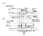
図8は、本発明の一実施例に従った一連の動作を行った際のSet/Resetセルの抵抗値の変化を示す図である。図8(a)は、メモリセル、及びダミーセルのプログラム抵抗値の変化を模式的に示し、図8(b)は、書込みの時の電流およびパルス幅を模式的に示している。 FIG. 8 is a diagram showing a change in the resistance value of the Set / Reset cell when a series of operations according to an embodiment of the present invention is performed. FIG. 8A schematically shows changes in program resistance values of the memory cell and the dummy cell, and FIG. 8B schematically shows current and pulse width at the time of writing.
初期書込み状態では、相変化素子の抵抗値は、RReset/Rsetにプログラムされている。通常アクセス状態において、書込み/読み出しが繰り返し行われる。 In the initial write state, the resistance value of the phase change element is programmed to RReset / Rset. In the normal access state, writing / reading is repeatedly performed.
Set状態の書込み(SW)を、iSet電流で、長いパルスにて繰り返されると、RSetは下がり、RSet’の状態となる。 When writing in the Set state (SW) is repeated with a long pulse at the iSet current, RSet is lowered to a state of RSet '.
次に、同一メモリセルに、Reset書込み(RW)を、iResetなる電流で、短いパルスで書込みを行っても、抵抗値は、RResetには戻らず、RReset’と低い抵抗値にResetされる。 Next, even if Reset writing (RW) is written to the same memory cell with a short pulse with a current iReset, the resistance value does not return to RReset, but is reset to a low resistance value, RReset '.
このとき、ダミーセルにも、同様のストレスがかかっており、比較回路111、112において、Set抵抗もしくはReset抵抗の低下が検出されれば、リフレッシュ要求回路107は、リフレッシュ要求を発行する。
At this time, the same stress is applied to the dummy cell, and if the
ここで、リフレッシュ動作に入り、一旦、メモリセルのデータを読み出し、データレジスタ105に一旦データを転送する。 Here, the refresh operation is started, the data in the memory cell is once read, and the data is once transferred to the data register 105.
しかる後、データレジスタ105の値を参照し、Set状態のセルのみ、Reset書込みを行う。 Thereafter, with reference to the value of the data register 105, Reset writing is performed only for the cells in the Set state.
ここで、ストレスの与えられてないResetセルの抵抗値は、RResetとなっており、ストレスが与えられている素子の抵抗値は、RReset’となる。 Here, the resistance value of the Reset cell to which stress is not applied is RReset, and the resistance value of the element to which stress is applied is RReset '.
次に、Verify ライト(VW)を行う。Verify用アンプ104には、1のデータをセットし、iSet>iVerifyなる電流にて、Set書込みを、Verifyリードしながら複数回行う。ここで、電流値を少なくしているのは、アモルファス状態から結晶化の進む速度を制御することで、抵抗値のばらつきを抑制する効果が得られると考えられるためである。
Next, Verify write (VW) is performed. 1 data is set in the verify
Verify用アンプ104にて、所望抵抗との電流比較を行い、所望抵抗に達したセルにおいては、書込みを中止し、そうでないものは、追加して書込みを行う。こうすることで、Reset抵抗にばらつきが発生しても、Setセルの抵抗を、RSetセルに揃えることができる。
The verify
この例では、Set電流値を下げる方法に関して説明したが、Setパルスの幅・印加時間の制御により、コントロールすることもできる。 In this example, the method for lowering the Set current value has been described, but it can also be controlled by controlling the width and application time of the Set pulse.
次に、再書込みにおいて、データレジスタの値を参照し、ResetセルのみResetを行い、抵抗値をRResetに揃えることができる。 Next, in rewriting, the value of the data register is referred to, and only the Reset cell is reset, so that the resistance value can be aligned with RReset.
前述した例においては、Set側に、一度合わせ込みを行い、Resetの再書込みを行うものについて説明したが、高電圧・高電流を印加して、Reset側での合わせ込みを行い、Setへの再書込みを実行することでも、上記と同様の作用効果を得ることができる。 In the above-described example, the description has been made on the Set side, and the Reset is rewritten. However, the high voltage and the high current are applied, the Reset side is adjusted, and the Set is set. The same effect as described above can be obtained by executing rewriting.
本実施例によれば、DRAMインターフェース互換のメモリであることを利用し、読み出し・書込み回数に応じたストレスを与えられる基準セルを設け、その基準セルの相変化素子抵抗値の変化を検出し、設定した基準値以上に抵抗値が変化していた場合(低抵抗化)、内部回路にリフレッシュ動作を要求する手段、もしくは、読み出し回数をカウントし、所望回数に応じて内部回路にリフレッシュ動作を要求する手段、もしくは、基準電流とメモリセルとに流れる電流の差を検出し、所望基準以上に抵抗値が変化していた場合に、内部回路にリフレッシュ動作を要求する手段を設け、メモリセルおよび基準セルを一旦リフレッシュする、もしくはメモリセルのみをリフレッシュすることにより、相変化素子のばらつきを補正することができるようにしたため、相変化素子のプログラム抵抗値のばらつきを補正し、マージン確保と同時にリテンション特性の改善を図ることができる。 According to this embodiment, using a DRAM interface compatible memory, a reference cell that can be stressed according to the number of reading / writing is provided, and a change in the resistance value of the phase change element of the reference cell is detected, If the resistance value has changed more than the set reference value (lower resistance), means to request a refresh operation from the internal circuit, or count the number of readings and request the internal circuit to perform a refresh operation according to the desired number of times Or a means for detecting a difference between the reference current and the current flowing through the memory cell and requesting a refresh operation to the internal circuit when the resistance value has changed more than a desired reference. Variations in phase change elements can be corrected by refreshing the cell once or refreshing only the memory cell. Since the way to correct the variation of the program resistance of the phase change element, it is possible to improve the simultaneous retention characteristic to the margins secured.
次に、本発明の第2の実施の形態について図面を参照して詳細に説明する。図12は、本発明の第2の実施の形態の構成を示す図である。図12を参照すると、コマンド入力回路1213のコマンド入力を起点として、読み出し回数を読み出しカウント回路1214にて、カウントを実施し、所定回数の読み出しが行われた場合、同様にして、リフレッシュ要求を行い、メモリセルのリフレッシュを行うことでも同様の効果を得られる。
Next, a second embodiment of the present invention will be described in detail with reference to the drawings. FIG. 12 is a diagram showing a configuration of the second exemplary embodiment of the present invention. Referring to FIG. 12, when the command input from the
図13は、本発明の第3の実施の形態の構成を示す図である。本実施の形態では、前記第1の実施の形態と相違して、ダミーセルを設けず、読み出し動作において、基準電流源から作られるSet基準電流回路1313と、Reset基準電流回路1314と、メモリセルを流れる電流とを比較し、所望のずれが発生した場合に、内部にリフレッシュを要求し、リフレッシュ期間において、前述したリフレッシュ動作を行う。
FIG. 13 is a diagram showing the configuration of the third exemplary embodiment of the present invention. In the present embodiment, unlike the first embodiment, dummy cells are not provided, and in a read operation, a Set reference
前記実施例で説明したリフレッシュ動作の例は、Reset/Setセルの抵抗を精度良く合わせ込みを行うことができる手法であるが、Verifyを行いながらの実行のため、処理時間がかかる。 The example of the refresh operation described in the above embodiment is a method that can accurately match the resistances of the Reset / Set cell. However, since the execution is performed while verifying, the processing time is required.
処理時間を短縮するためのリフレッシュ方法の実施例を、図14に示す。図14に示すように、リフレッシュ動作の別の実施例は、リフレッシュ要求は、前述した第1、2、3実施の形態のリフレッシュ判定手法のいずれかにより、判定され、
1)Reset/Setセルの読み出しを行う。
An embodiment of a refresh method for shortening the processing time is shown in FIG. As shown in FIG. 14, in another example of the refresh operation, the refresh request is determined by any of the refresh determination methods of the first, second, and third embodiments described above,
1) Read the Reset / Set cell.
2)Resetセルであれば、通常、Reset動作時より大きな電流・電圧を与えることで、Reset上書きを行い、RReset+αの高抵抗状態とする。 2) In the case of a Reset cell, a reset current is normally overwritten by applying a larger current / voltage than that at the time of the Reset operation, and a high resistance state of RReset + α is obtained.
ここでは、iReset+αなる電流を流し、ジュール熱による発熱により結晶を融解し、より高抵抗のアモルファス状態としている。 Here, a current of iReset + α is passed, and the crystal is melted by heat generation due to Joule heat, so that the amorphous state has a higher resistance.
3) 上書きされたResetセルは、Set状態に書込み(低抵抗)した後、再度通常電流・電圧のResetに書き戻す。 3) The overwritten Reset cell is written to the Set state (low resistance) and then written back to the normal current / voltage Reset again.
4) Setセルであれば、通常Reset動作時より大きな電流・電圧を与えることで、RReset+αの高抵抗状態にした後、再度Setに書き戻しを行う。 4) In the case of a Set cell, a larger current / voltage than that in the normal Reset operation is applied to bring the RReset + α into a high resistance state, and then writing back to the Set is performed again.
一般に、Reset時間<Set時間であり、前述したリフレッシュ方法では、メモリセルの状態が所望のSetレベルに至るまで、Set動作を複数回実行する必要がある。 Generally, Reset time <Set time, and in the refresh method described above, it is necessary to execute the Set operation a plurality of times until the state of the memory cell reaches a desired Set level.
第2のリフレッシュ方式においては、少なくとも2回のReset動作と、1回のSet動作で処理を終了できるため、短時間でのリフレッシュが可能であるが、第1のリフレッシュ方式と比較すると、抵抗値の合わせ込み精度は多少劣る。 In the second refresh method, since the process can be completed by at least two reset operations and one set operation, the refresh can be performed in a short time. However, the resistance value is lower than that in the first refresh method. The fitting accuracy is slightly inferior.
しかしながら、第2のリフレッシュ方法によっても、所望の抵抗値からの変動を検知し、抵抗値の補正をかけることができるため、問題であるリテンション特性の向上を図ることができる。 However, the second refresh method can also detect the fluctuation from the desired resistance value and correct the resistance value, so that the problem of the retention characteristic can be improved.
上記した例では、一旦、全てReset側に合わせ込みを行ったが、Set側へ合わせ込みを行った後に、大電流により、RResetに抵抗を合わせ込み、しかる後に、Set側に再書込みを行っても、上記と同様の作用効果を得ることができる。 In the above example, all adjustments were once made to the Reset side, but after adjustments were made to the Set side, resistance was adjusted to the RReset by a large current, and then rewriting was performed to the Set side. Also, the same effect as described above can be obtained.
以上本発明を上記実施形態に即して説明したが、本発明は、上記実施形態の構成にのみ限定されるものでなく、本発明の範囲内で当業者であればなし得るであろう各種変形、修正を含むことは勿論である。 The present invention has been described with reference to the above embodiment, but the present invention is not limited to the configuration of the above embodiment, and various modifications that can be made by those skilled in the art within the scope of the present invention. Of course, including modifications.
101 メモリセル
102 センスアンプ
103 ライトアンプ
104 Verify用アンプ
105 データレジスタ
106 ライトパルス制御回路
107 リフレッシュ要求回路
108 ダミーセルライトアンプ
109 Setダミーセル
110 Resetダミーセル
111 Set比較回路
112 Reset比較回路
301 Setセル
302 バイアス回路
303 定電流源
401 Resetセル
402 バイアス回路
403 定電流源
502 バイアス回路
503 定電流源
602 バイアス回路
603 定電流源
1101 上部電極
1102 下部電極
1103 Agなどを含む固体電解質
1213 コマンド入力回路
1214 読み出しカウント回路
1313 Set基準電流回路
1314 Reset基準電流回路
DESCRIPTION OF
1314 Reset reference current circuit
Claims (9)
前記抵抗素子は相変化材料を用いて形成されており、
前記抵抗素子の抵抗値の変化に応じて、前記メモリセルのリフレッシュ動作を行うように制御する制御回路と、
リフレッシュ対象の前記メモリセルから読み出された第1の状態または第2の状態のデータが転送され保持するデータレジスタと、
リフレッシュ時に、前記第2の状態のセルを、段階的に、前記第1の状態にプログラムするライト・パルス制御回路とを備え、
リフレッシュ時に、前記データレジスタの値を参照し、前記第1の状態のセルのみを一旦前記第2の状態に変更した後に、前記ライト・パルス制御回路によって前記第2の状態のセルを、段階的に、前記第1の状態にプログラムし、
全てのセルが前記第1の状態となったら、前記データレジスタの値を参照して、前記第2の状態のデータを保持していたセルのみを前記第2の状態に変更することを特徴とするメモリ装置。 A memory cell including a programmable resistance element is provided at the intersection of the bit line and the word line,
The resistance element is formed using a phase change material,
A control circuit for controlling the memory cell to perform a refresh operation according to a change in the resistance value of the resistance element ;
A data register in which data in the first state or the second state read from the memory cell to be refreshed is transferred and held;
A write pulse control circuit for programming the cells in the second state to the first state step by step during refresh;
At the time of refresh, after referring to the value of the data register and changing only the cells in the first state to the second state, the cells in the second state are changed stepwise by the write pulse control circuit. Programming to the first state;
When all the cells are in the first state, the value of the data register is referred to and only the cell holding the data in the second state is changed to the second state. Memory device.
前記抵抗素子は相変化材料を用いて形成されており、
前記抵抗素子の抵抗値の変化に応じて、前記メモリセルのリフレッシュ動作を行うように制御する制御回路と、
リフレッシュ対象の前記メモリセルから読み出された第1の状態または第2の状態のデータが転送され保持するデータレジスタとを備え、
リフレッシュ時に、前記データレジスタの値を参照して、前記第2の状態のセルのみに通常動作時よりも大きな電流または電圧を印加して前記第2の状態の上書きを行い、前記第1の状態のセルのみに通常動作時よりも大きな電流または電圧を印加して前記第2の状態とし、リフレッシュ対象の全てのセルが前記第2の状態となった後に、全てのセルを前記第1の状態に変更し、前記データレジスタの値を参照して前記第2の状態を保持していたセルのみを前記第2の状態に変更することを特徴とするメモリ装置。 A memory cell including a programmable resistance element is provided at the intersection of the bit line and the word line,
The resistance element is formed using a phase change material,
A control circuit for controlling the memory cell to perform a refresh operation according to a change in the resistance value of the resistance element;
A data register in which data in the first state or the second state read from the memory cell to be refreshed is transferred and held;
At the time of refresh, with reference to the value of the data register, the second state is overwritten by applying a larger current or voltage to only the cells in the second state than in the normal operation, and the first state A current or voltage larger than that in normal operation is applied to only the cells in the second state, and all the cells to be refreshed enter the second state, and then all the cells are in the first state. The memory device is characterized in that, by referring to the value of the data register, only the cell that has held the second state is changed to the second state .
前記抵抗素子は相変化材料を用いて形成されており、
前記抵抗素子の抵抗値の変化に応じて、前記メモリセルのリフレッシュ動作を行うように制御する制御回路と、
リフレッシュ対象の前記メモリセルから読み出された第1の状態または第2の状態のデータが転送され保持するデータレジスタとを備え、
リフレッシュ時に、前記データレジスタの値を参照し、前記第2の状態のセルのみを前記第1の状態に変更し、リフレッシュ対象のセルが全て前記第1の状態となったら通常動作時よりも大きな電流または電圧を印加してリフレッシュ対象のセルを全て前記第2の状態とした後に、前記データレジスタの値を参照して前記第1の状態を保持していたセルのみを前記第1の状態に変更することを特徴とするメモリ装置。 A memory cell including a programmable resistance element is provided at the intersection of the bit line and the word line,
The resistance element is formed using a phase change material,
A control circuit for controlling the memory cell to perform a refresh operation according to a change in the resistance value of the resistance element;
A data register in which data in the first state or the second state read from the memory cell to be refreshed is transferred and held;
At the time of refresh, the value of the data register is referred to, and only the cells in the second state are changed to the first state. When all the cells to be refreshed are in the first state, the value is larger than that in the normal operation. After all the cells to be refreshed are applied to the second state by applying a current or voltage, only the cells that have held the first state with reference to the value of the data register are set to the first state. A memory device characterized by being changed .
相変化素子を含み、読み出し・書込み回数に応じたストレスが与えられるダミーセルと、
前記ダミーセルの相変化素子の抵抗値の変化を検出する回路と、
前記ダミーセルの相変化素子が予め設定された基準値以上に抵抗値が変化していた場合に、リフレッシュ要求を行うリフレッシュ要求手段と、
を備え、前記リフレッシュ要求に基づき、前記メモリセル及びダミーセルをリフレッシュし、
リフレッシュ時に前記メモリセルから読み出されたデータを保持するデータレジスタと、
リフレッシュ時に前記メモリセルのデータの書込み状態を比較・検出するベリファイアンプと、を備え、
リフレッシュ時、前記メモリセルのデータを読み出し前記データレジスタに一旦データを転送したのち、前記データレジスタの値を参照し、第1の状態のセルのみ、第2の状態の書込みを行い、
前記ベリファイアンプには第1の状態データをセットし、第1の状態の書込みを、
ベリファイリードしながら行い、所望抵抗との電流比較を行い、所望抵抗に達したセルにおいては、書込みを中止し、そうでないものは、追加して書込みを行い、
次に、再書込みにおいて、前記データレジスタの値を参照し第2の状態のセルのみ第2の状態の書き込みを行う、ことを特徴とするメモリ装置。 In a memory device including a plurality of memory cells including phase change elements,
A dummy cell that includes a phase change element and is subjected to stress according to the number of reading / writing operations;
A circuit for detecting a change in resistance value of the phase change element of the dummy cell;
Refresh request means for making a refresh request when the resistance value of the phase change element of the dummy cell has changed more than a preset reference value;
And refreshing the memory cell and the dummy cell based on the refresh request ,
A data register for holding data read from the memory cells during refresh;
A verify amplifier that compares and detects the data write state of the memory cell during refresh,
At the time of refreshing, the data in the memory cell is read and transferred once to the data register, and then the value in the data register is referred to, and only the cell in the first state is written in the second state,
First state data is set in the verify amplifier, and writing of the first state is performed.
While verify-reading, compare the current with the desired resistance, and in the cell that has reached the desired resistance, stop writing, and if not, perform additional writing,
Next, in the rewriting, the memory device is characterized in that the second state is written only to the cell in the second state with reference to the value of the data register.
読み出し回数をカウントするカウンタと、
読み出し回数をモニタして所定回数に達した時に、前記メモリセルのリフレッシュ要求を行う手段と、
を備えており、
リフレッシュ時、前記メモリセルのデータを読み出し前記データレジスタに一旦データを転送したのち、前記データレジスタの値を参照し、第1の状態のセルのみ、第2の状態の書込みを行い、
前記ベリファイアンプには第1の状態データをセットし、第1の状態の書込みを、ベリファイリードしながら行い、所望抵抗との電流比較を行い、所望抵抗に達したセルにおいては、書込みを中止し、そうでないものは、追加して書込みを行い、
次に、再書込みにおいて、前記データレジスタの値を参照し第2の状態のセルのみ第2の状態の書き込みを行う、ことを特徴とするメモリ装置。 In a memory device including a plurality of memory cells including phase change elements,
A counter that counts the number of reads;
Means for making a refresh request for the memory cell when the predetermined number of times is monitored by monitoring the number of reads;
With
At the time of refreshing, the data in the memory cell is read and transferred once to the data register, and then the value in the data register is referred to, and only the cell in the first state is written in the second state,
The first state data is set in the verify amplifier, writing in the first state is performed while verify reading is performed, current comparison with the desired resistance is performed, and writing is stopped in a cell that has reached the desired resistance. , If not, add and write,
Next, in the rewriting, the memory device is characterized in that the second state is written only to the cell in the second state with reference to the value of the data register.
前記メモリセルの第1の状態と第2の状態にそれぞれ対応する第1、第2の基準電流を供給する第1、第2の基準電流回路と、
前記メモリセルを流れる電流と前記第1、第2の基準電流を比較し、所望のずれが発生した場合に、リフレッシュ要求を行うリフレッシュ要求手段と、
を備え、
前記リフレッシュ要求に基づき、メモリセルをリフレッシュし、
リフレッシュ時に、前記第1または第2の状態のセルの読み出しを行い、
前記第2の状態のセルであれば、通常動作時よりも大きな電圧または電流を印加して、前記第2の状態の上書きを行い、上書きされた第2の状態のセルは、第1の状態に書込みした後、再度、通常電流・電圧の第2の状態に書き戻し、
前記第1の状態のセルであれば、通常動作時よりも大きな電圧または電流を印加して前記第2の状態にした後、再度第1の状態に書き戻しを行う、ことを特徴とするメモリ装置。 In a memory device including a plurality of memory cells including phase change elements,
First and second reference current circuits for supplying first and second reference currents respectively corresponding to the first state and the second state of the memory cell ;
A refresh request means for comparing a current flowing through the memory cell with the first and second reference currents and performing a refresh request when a desired deviation occurs;
With
Based on the refresh request, refresh the memory cell;
When refreshing, reading the cells in the first or second state,
If the cell is in the second state, the second state is overwritten by applying a voltage or current larger than that in the normal operation, and the overwritten second state cell is in the first state. After writing to, write back to the second state of normal current and voltage again,
If the cell is in the first state, a voltage or current larger than that in the normal operation is applied to make the second state, and then the memory is written back to the first state again. apparatus.
リフレッシュ時に前記メモリセルのデータの書込み状態を比較・検出するベリファイアンプと、を備え、
読み出し・書込み回数に応じたストレスが与えられるダミーセルの相変化素子の抵抗値の変化を検出する工程と、
前記ダミーセルの相変化素子が予め設定された基準値以上に抵抗値が変化していた場合に、内部回路に対してリフレッシュ要求を行う工程と、
前記リフレッシュ要求に基づき、前記メモリセルおよび前記ダミーセルをリフレッシュする工程と、
リフレッシュ時、前記メモリセルのデータを読み出し、前記データレジスタに一旦データを転送したのち、前記データレジスタの値を参照し、第1の状態のセルのみ、第2の状態の書込みを行う工程と、
前記メモリセルのデータの書込み状態を比較・検出するベリファイアンプに、第1の状態データをセットし、第1の状態の書込みを、ベリファイリードしながら行い、所望抵抗との電流比較を行い、所望抵抗に達したセルにおいては、書込みを中止し、そうでないものは、追加して書込みを行う工程と、
次に、再書込みにおいて、前記データレジスタの値を参照し、第2の状態のセルのみ第2の状態の書き込みを行う工程と、
を含むことを特徴とするメモリ装置のリフレッシュ方法。 A data register for holding data read from a memory cell including a phase change element during refresh;
A verify amplifier that compares and detects the data write state of the memory cell during refresh,
Detecting a change in resistance value of the phase change element of the dummy cell to which stress is applied according to the number of reading / writing times;
A step of making a refresh request to the internal circuit when the resistance value of the phase change element of the dummy cell has changed more than a preset reference value;
Based on the refresh request, the steps of refreshing the memory cells and the dummy cells,
At the time of refreshing, reading the data of the memory cell, transferring the data to the data register once, referring to the value of the data register, and writing the second state only to the cell in the first state;
The first state data is set in a verify amplifier that compares and detects the data write state of the memory cell, the first state write is performed while verify read, and a current comparison with a desired resistance is performed. In the cell that has reached the resistance, writing is stopped, and if not, writing is additionally performed, and
Next, in rewriting, referring to the value of the data register and writing the second state only to the cells in the second state;
A method for refreshing a memory device, comprising:
リフレッシュ時に前記メモリセルのデータの書込み状態を比較・検出するベリファイアンプと、を備え、
前記メモリセルの読み出し回数をカウントする工程と、
読み出し回数をモニタして所定回数に達した時に、内部回路に対してリフレッシュ要求する工程と、
リフレッシュ時、前記メモリセルのデータを読み出しデータレジスタに一旦データを転送したのち、前記データレジスタの値を参照し、第1の状態のセルのみ、第2の状態の書込みを行う工程と、
前記メモリセルのデータの書込み状態を比較・検出するベリファイアンプに、第1の状態データをセットし、第1の状態の書込みを、ベリファイリードしながら行い、所望抵抗との電流比較を行い、所望抵抗に達したセルにおいては、書込みを中止し、そうでないものは、追加して書込みを行う工程と、
次に、再書込みにおいて、前記データレジスタの値を参照し、第2の状態のセルのみ第2の状態の書き込みを行う工程と、
を含むことを特徴とするメモリ装置のリフレッシュ方法。 A data register for holding data read from a memory cell including a phase change element during refresh;
A verify amplifier that compares and detects the data write state of the memory cell during refresh,
A step of counting the number of times of reading of the memory cell,
A process of requesting a refresh to the internal circuit when the number of readings is monitored and reaches a predetermined number of times ;
At the time of refresh, reading the data of the memory cell, transferring the data to the data register once, referring to the value of the data register, and writing the second state only to the cell in the first state;
The first state data is set in a verify amplifier that compares and detects the data write state of the memory cell, the first state write is performed while verify read, and a current comparison with a desired resistance is performed. In the cell that has reached the resistance, writing is stopped, and if not, writing is additionally performed, and
Next, the rewrite, the steps of the de-reference the value of Tarejisuta writes the second state only the cell in the second state,
A method for refreshing a memory device, comprising:
前記メモリセルを流れる電流に所望のずれが発生した場合に、内部回路に対して、
リフレッシュを要求する工程と、
リフレッシュ要求に基づき、メモリセルをリフレッシュする工程と、
前記第1または第2の状態のセルを読み出す工程と、
第2の状態のセルであれば、通常動作時よりも大きな電圧または電流を印加して第2の状態の上書きを行い、上書きされた第2の状態のセルは、第1の状態に書込みした後、再度、通常電流・電圧の第2の状態に書き戻す工程と、
第1の状態のセルであれば、通常動作時よりも大きな電圧または電流を印加して第2の状態にした後、再度第1の状態に書き戻しを行う工程と、
を含む、ことを特徴とするメモリ装置のリフレッシュ方法。 Comparing first and second reference currents respectively corresponding to a first state and a second state of a memory cell including a phase change element, and a current flowing through the memory cell;
When a desired deviation occurs in the current flowing through the memory cell,
A process requesting a refresh;
Refreshing the memory cell based on the refresh request;
Reading the cells in the first or second state;
If the cell is in the second state, the second state is overwritten by applying a voltage or current larger than that in the normal operation, and the overwritten second state cell is written in the first state. After that, a step of writing back to the second state of the normal current / voltage again,
If the cell is in the first state, a step of applying a voltage or current larger than that during normal operation to the second state and then writing back to the first state again;
A refresh method for a memory device, comprising:
Priority Applications (6)
| Application Number | Priority Date | Filing Date | Title |
|---|---|---|---|
| JP2005011626A JP4282612B2 (en) | 2005-01-19 | 2005-01-19 | Memory device and refresh method thereof |
| DE102006000618A DE102006000618A1 (en) | 2005-01-19 | 2006-01-02 | storage device |
| CNB2006100050858A CN100530423C (en) | 2005-01-19 | 2006-01-17 | Memory device |
| US11/333,344 US20060158948A1 (en) | 2005-01-19 | 2006-01-18 | Memory device |
| US12/207,077 US7580277B2 (en) | 2005-01-19 | 2008-09-09 | Memory device including a programmable resistance element |
| US12/500,673 US7751227B2 (en) | 2005-01-19 | 2009-07-10 | Memory device including a programmable resistance element |
Applications Claiming Priority (1)
| Application Number | Priority Date | Filing Date | Title |
|---|---|---|---|
| JP2005011626A JP4282612B2 (en) | 2005-01-19 | 2005-01-19 | Memory device and refresh method thereof |
Publications (2)
| Publication Number | Publication Date |
|---|---|
| JP2006202383A JP2006202383A (en) | 2006-08-03 |
| JP4282612B2 true JP4282612B2 (en) | 2009-06-24 |
Family
ID=36683718
Family Applications (1)
| Application Number | Title | Priority Date | Filing Date |
|---|---|---|---|
| JP2005011626A Expired - Fee Related JP4282612B2 (en) | 2005-01-19 | 2005-01-19 | Memory device and refresh method thereof |
Country Status (4)
| Country | Link |
|---|---|
| US (3) | US20060158948A1 (en) |
| JP (1) | JP4282612B2 (en) |
| CN (1) | CN100530423C (en) |
| DE (1) | DE102006000618A1 (en) |
Families Citing this family (77)
| Publication number | Priority date | Publication date | Assignee | Title |
|---|---|---|---|---|
| JP4282612B2 (en) * | 2005-01-19 | 2009-06-24 | エルピーダメモリ株式会社 | Memory device and refresh method thereof |
| US20070279975A1 (en) * | 2006-06-06 | 2007-12-06 | Hudgens Stephen J | Refreshing a phase change memory |
| US7405964B2 (en) * | 2006-07-27 | 2008-07-29 | Qimonda North America Corp. | Integrated circuit to identify read disturb condition in memory cell |
| JP2008071384A (en) | 2006-09-12 | 2008-03-27 | Elpida Memory Inc | Semiconductor storage device |
| KR100819106B1 (en) * | 2006-09-27 | 2008-04-02 | 삼성전자주식회사 | How Writes Work in Phase Change Memory Devices |
| JPWO2008041278A1 (en) * | 2006-09-29 | 2010-01-28 | 株式会社ルネサステクノロジ | Semiconductor device |
| US7623401B2 (en) * | 2006-10-06 | 2009-11-24 | Qimonda North America Corp. | Semiconductor device including multi-bit memory cells and a temperature budget sensor |
| US7679980B2 (en) * | 2006-11-21 | 2010-03-16 | Qimonda North America Corp. | Resistive memory including selective refresh operation |
| US7539050B2 (en) * | 2006-11-22 | 2009-05-26 | Qimonda North America Corp. | Resistive memory including refresh operation |
| US7474579B2 (en) * | 2006-12-20 | 2009-01-06 | Spansion Llc | Use of periodic refresh in medium retention memory arrays |
| US8164941B2 (en) * | 2006-12-27 | 2012-04-24 | Hynix Semiconductor Inc. | Semiconductor memory device with ferroelectric device and refresh method thereof |
| US7548467B2 (en) * | 2006-12-28 | 2009-06-16 | Samsung Electronics Co., Ltd. | Bias voltage generator and method generating bias voltage for semiconductor memory device |
| KR100850290B1 (en) * | 2007-01-11 | 2008-08-04 | 삼성전자주식회사 | Multi -level bias voltage generator and semiconductor memory device having the same |
| TWI320180B (en) * | 2007-01-12 | 2010-02-01 | A driving method and a driving system for writing the phase change memory | |
| JP2008181380A (en) * | 2007-01-25 | 2008-08-07 | Toshiba Corp | Memory system and control method thereof |
| CN101266834B (en) * | 2007-03-15 | 2012-07-04 | 西格斯教育资本有限责任公司 | Writing drive method and system for phase change memory |
| KR100887138B1 (en) * | 2007-08-10 | 2009-03-04 | 주식회사 하이닉스반도체 | Driving Method of Phase Change Memory Device |
| KR20090086816A (en) | 2008-02-11 | 2009-08-14 | 삼성전자주식회사 | Phase change memory device, its writing method, and system comprising it |
| US8767450B2 (en) | 2007-08-21 | 2014-07-01 | Samsung Electronics Co., Ltd. | Memory controllers to refresh memory sectors in response to writing signals and memory systems including the same |
| US7961534B2 (en) * | 2007-09-10 | 2011-06-14 | Hynix Semiconductor Inc. | Semiconductor memory device for writing data to multiple cells simultaneously and refresh method thereof |
| US7675792B2 (en) * | 2007-09-26 | 2010-03-09 | Intel Corporation | Generating reference currents compensated for process variation in non-volatile memories |
| JP2009087509A (en) | 2007-10-03 | 2009-04-23 | Toshiba Corp | Semiconductor memory device |
| JP5049733B2 (en) * | 2007-10-17 | 2012-10-17 | 株式会社東芝 | Information processing system |
| US20090046499A1 (en) * | 2008-02-05 | 2009-02-19 | Qimonda Ag | Integrated circuit including memory having limited read |
| KR20100064714A (en) | 2008-12-05 | 2010-06-15 | 삼성전자주식회사 | Nonvolatile memory device using variable resistive element |
| US8391051B2 (en) | 2009-04-10 | 2013-03-05 | Panasonic Corporation | Method of programming nonvolatile memory element |
| US8031518B2 (en) * | 2009-06-08 | 2011-10-04 | Micron Technology, Inc. | Methods, structures, and devices for reducing operational energy in phase change memory |
| US8406033B2 (en) | 2009-06-22 | 2013-03-26 | Macronix International Co., Ltd. | Memory device and method for sensing and fixing margin cells |
| US7894254B2 (en) * | 2009-07-15 | 2011-02-22 | Macronix International Co., Ltd. | Refresh circuitry for phase change memory |
| US8984572B2 (en) | 2009-07-24 | 2015-03-17 | Koninklijke Philips N.V. | Method and system for transmitting channels to at least one digital video recorder |
| US9135277B2 (en) | 2009-08-07 | 2015-09-15 | Google Inc. | Architecture for responding to a visual query |
| US8351289B1 (en) | 2009-12-30 | 2013-01-08 | Micron Technology, Inc. | Apparatuses and methods for sensing a phase-change test cell and determining changes to the test cell resistance due to thermal exposure |
| CN103222005B (en) * | 2009-12-31 | 2016-08-24 | 美光科技公司 | Method for phase change memory array |
| US8634235B2 (en) | 2010-06-25 | 2014-01-21 | Macronix International Co., Ltd. | Phase change memory coding |
| JPWO2012039415A1 (en) | 2010-09-21 | 2014-02-03 | 日本電気株式会社 | Semiconductor device and control method thereof |
| US8467238B2 (en) | 2010-11-15 | 2013-06-18 | Macronix International Co., Ltd. | Dynamic pulse operation for phase change memory |
| US8374019B2 (en) | 2011-01-05 | 2013-02-12 | Macronix International Co., Ltd. | Phase change memory with fast write characteristics |
| JP5858036B2 (en) | 2011-03-02 | 2016-02-10 | 日本電気株式会社 | Reconfigurable circuit |
| US9324433B2 (en) * | 2011-04-25 | 2016-04-26 | Microsoft Technology Licensing, Llc | Intelligent flash reprogramming |
| US8891293B2 (en) | 2011-06-23 | 2014-11-18 | Macronix International Co., Ltd. | High-endurance phase change memory devices and methods for operating the same |
| CN104115230B (en) * | 2011-12-22 | 2018-02-16 | 英特尔公司 | Computing device, method and system based on High Efficiency PC MS flush mechanisms |
| JP5763004B2 (en) * | 2012-03-26 | 2015-08-12 | 株式会社東芝 | Nonvolatile semiconductor memory device |
| US8743600B2 (en) * | 2012-04-24 | 2014-06-03 | Being Advanced Memory Corporation | Processors and systems using cell-refreshed phase-change memory |
| US9001550B2 (en) | 2012-04-27 | 2015-04-07 | Macronix International Co., Ltd. | Blocking current leakage in a memory array |
| KR20140026889A (en) * | 2012-08-23 | 2014-03-06 | 삼성전자주식회사 | Resistive memory device performing selective refresh and method of refreshing the resistive memeory device |
| US8957700B2 (en) * | 2012-09-28 | 2015-02-17 | Analog Devices, Inc. | Apparatus and methods for digital configuration of integrated circuits |
| EP2923358A4 (en) * | 2012-11-20 | 2016-06-29 | Charles I Peddle | Solid state drive architectures |
| US11037625B2 (en) | 2012-11-20 | 2021-06-15 | Thstyme Bermuda Limited | Solid state drive architectures |
| KR20140080945A (en) * | 2012-12-21 | 2014-07-01 | 에스케이하이닉스 주식회사 | Non-volatile memory apparatus |
| KR102055375B1 (en) * | 2013-01-14 | 2020-01-22 | 삼성전자 주식회사 | Nonvolatile memory device using variable resistive element and memory system comprising the same |
| US8964442B2 (en) | 2013-01-14 | 2015-02-24 | Macronix International Co., Ltd. | Integrated circuit 3D phase change memory array and manufacturing method |
| CN103440880A (en) * | 2013-09-03 | 2013-12-11 | 苏州宽温电子科技有限公司 | SRAM (Static Random Access Memory) and bit cell tracking method |
| US9384801B2 (en) | 2014-08-15 | 2016-07-05 | Intel Corporation | Threshold voltage expansion |
| US9595354B2 (en) | 2014-12-15 | 2017-03-14 | Infineon Technologies Ag | Nonvolatile memory refresh |
| US10438658B2 (en) * | 2014-12-26 | 2019-10-08 | Intel Corporation | Refresh logic to refresh only memory cells having a first value |
| US20160306569A1 (en) * | 2015-02-25 | 2016-10-20 | Kabushiki Kaisha Toshiba | Memory system |
| US9472274B1 (en) * | 2015-07-01 | 2016-10-18 | Macronix International Co., Ltd. | Refresh of nonvolatile memory cells and reference cells with resistance drift |
| JP2017021877A (en) * | 2015-07-13 | 2017-01-26 | ソニー株式会社 | Nonvolatile memory, memory controller, storage device, information processing system, and nonvolatile memory control method |
| CN105023606B (en) * | 2015-08-14 | 2018-06-26 | 中国科学院上海微系统与信息技术研究所 | A kind of phase transition storage and its method for restoring data |
| US9779810B2 (en) | 2015-09-11 | 2017-10-03 | Macronix International Co., Ltd. | Adjustable writing circuit |
| KR102373544B1 (en) | 2015-11-06 | 2022-03-11 | 삼성전자주식회사 | Memory Device and Memory System Performing Request-based Refresh and Operating Method of Memory Device |
| CN105810242A (en) * | 2016-03-02 | 2016-07-27 | 中国科学院上海微系统与信息技术研究所 | Phase change memory and operation method for improving fatigue life of same |
| JP2017174484A (en) * | 2016-03-25 | 2017-09-28 | ルネサスエレクトロニクス株式会社 | Semiconductor storage device |
| CN105931665B (en) * | 2016-04-19 | 2020-06-09 | 中国科学院上海微系统与信息技术研究所 | Phase change memory reading circuit and method |
| KR102559530B1 (en) | 2016-09-19 | 2023-07-27 | 에스케이하이닉스 주식회사 | Resistance Variable Memory Apparatus, Circuit and Method for Preventing of Disturbance Therefor |
| US10147475B1 (en) * | 2017-05-09 | 2018-12-04 | Micron Technology, Inc. | Refresh in memory based on a set margin |
| US10319437B2 (en) * | 2017-09-20 | 2019-06-11 | Sandisk Technologies Llc | Apparatus and method for identifying memory cells for data refresh based on monitor cell in a resistive memory device |
| US10706920B2 (en) | 2017-11-02 | 2020-07-07 | Samsung Electronics Co., Ltd. | Memory device |
| CN108878646A (en) * | 2018-06-28 | 2018-11-23 | 北京大学 | A kind of resistive device multistage stabilization resistance state implementation method and electronic equipment |
| US11055226B2 (en) * | 2018-06-29 | 2021-07-06 | Intel Corporation | Mitigation of cache-latency based side-channel attacks |
| JP2020149736A (en) * | 2019-03-11 | 2020-09-17 | キオクシア株式会社 | Semiconductor storage device |
| US10943657B1 (en) * | 2019-08-19 | 2021-03-09 | Micron Technology, Inc. | Mitigation of voltage threshold drift associated with power down condition of non-volatile memory device |
| US11139016B1 (en) | 2020-04-07 | 2021-10-05 | Micron Technology, Inc. | Read refresh operation |
| US11404120B2 (en) | 2020-05-13 | 2022-08-02 | Micron Technology, Inc. | Refresh operation of a memory cell |
| WO2022222310A1 (en) * | 2021-04-20 | 2022-10-27 | 芯盟科技有限公司 | Transistor and manufacturing method therefor, and semiconductor device and manufacturing method therefor |
| US11538522B1 (en) * | 2021-06-30 | 2022-12-27 | Micron Technology, Inc. | Systems and methods for adaptive self-referenced reads of memory devices |
| CN114783485B (en) * | 2022-06-21 | 2022-10-18 | 阿里云计算有限公司 | Method for refreshing phase change memory and phase change memory device |
Family Cites Families (17)
| Publication number | Priority date | Publication date | Assignee | Title |
|---|---|---|---|---|
| US5270967A (en) | 1991-01-16 | 1993-12-14 | National Semiconductor Corporation | Refreshing ferroelectric capacitors |
| US6141241A (en) * | 1998-06-23 | 2000-10-31 | Energy Conversion Devices, Inc. | Universal memory element with systems employing same and apparatus and method for reading, writing and programming same |
| JP3866511B2 (en) | 2000-12-22 | 2007-01-10 | 東芝マイクロエレクトロニクス株式会社 | Non-volatile memory |
| US6646902B2 (en) * | 2001-08-30 | 2003-11-11 | Micron Technology, Inc. | Method of retaining memory state in a programmable conductor RAM |
| US6560155B1 (en) * | 2001-10-24 | 2003-05-06 | Micron Technology, Inc. | System and method for power saving memory refresh for dynamic random access memory devices after an extended interval |
| JP2003141873A (en) | 2001-11-05 | 2003-05-16 | Toshiba Corp | Magnetic storage device |
| JP2004062922A (en) * | 2002-07-25 | 2004-02-26 | Renesas Technology Corp | Nonvolatile semiconductor memory device |
| US6768665B2 (en) * | 2002-08-05 | 2004-07-27 | Intel Corporation | Refreshing memory cells of a phase change material memory device |
| JP4134637B2 (en) | 2002-08-27 | 2008-08-20 | 株式会社日立製作所 | Semiconductor device |
| JP4129170B2 (en) | 2002-12-05 | 2008-08-06 | シャープ株式会社 | Semiconductor memory device and memory data correction method for memory cell |
| JP4256175B2 (en) * | 2003-02-04 | 2009-04-22 | 株式会社東芝 | Nonvolatile semiconductor memory |
| JP2004348802A (en) * | 2003-05-20 | 2004-12-09 | Sharp Corp | Program verification method for nonvolatile memory element, semiconductor storage device, and portable electronic device having the same |
| US7085154B2 (en) | 2003-06-03 | 2006-08-01 | Samsung Electronics Co., Ltd. | Device and method for pulse width control in a phase change memory device |
| US6961277B2 (en) * | 2003-07-08 | 2005-11-01 | Micron Technology, Inc. | Method of refreshing a PCRAM memory device |
| JP4322645B2 (en) * | 2003-11-28 | 2009-09-02 | 株式会社日立製作所 | Semiconductor integrated circuit device |
| US20060056251A1 (en) * | 2004-09-10 | 2006-03-16 | Parkinson Ward D | Using a phase change memory as a replacement for a dynamic random access memory |
| JP4282612B2 (en) * | 2005-01-19 | 2009-06-24 | エルピーダメモリ株式会社 | Memory device and refresh method thereof |
-
2005
- 2005-01-19 JP JP2005011626A patent/JP4282612B2/en not_active Expired - Fee Related
-
2006
- 2006-01-02 DE DE102006000618A patent/DE102006000618A1/en not_active Withdrawn
- 2006-01-17 CN CNB2006100050858A patent/CN100530423C/en not_active Expired - Fee Related
- 2006-01-18 US US11/333,344 patent/US20060158948A1/en not_active Abandoned
-
2008
- 2008-09-09 US US12/207,077 patent/US7580277B2/en not_active Expired - Fee Related
-
2009
- 2009-07-10 US US12/500,673 patent/US7751227B2/en not_active Expired - Fee Related
Also Published As
| Publication number | Publication date |
|---|---|
| US20090010048A1 (en) | 2009-01-08 |
| JP2006202383A (en) | 2006-08-03 |
| US7751227B2 (en) | 2010-07-06 |
| US7580277B2 (en) | 2009-08-25 |
| DE102006000618A1 (en) | 2006-08-17 |
| CN1811985A (en) | 2006-08-02 |
| US20060158948A1 (en) | 2006-07-20 |
| US20090273970A1 (en) | 2009-11-05 |
| CN100530423C (en) | 2009-08-19 |
Similar Documents
| Publication | Publication Date | Title |
|---|---|---|
| JP4282612B2 (en) | Memory device and refresh method thereof | |
| KR100773095B1 (en) | Phase change memory device and its programming method | |
| JP5148946B2 (en) | Write operation method in phase change memory device | |
| JP4570886B2 (en) | Phase change memory device | |
| US7907437B2 (en) | Resistance variable memory device and method of writing data | |
| KR101374319B1 (en) | Resistance variable memory device and operation method thereof | |
| CN106504785B (en) | Memory device for resistance drift recovery and method of operating the same | |
| JP5520522B2 (en) | Phase change memory device and reading method thereof | |
| KR101025053B1 (en) | Semiconductor device | |
| KR20090020342A (en) | Variable resistance memory device and its programming method | |
| US20090040814A1 (en) | Method for driving multi-level data to a phase change memory device | |
| KR20110027939A (en) | Phase change memory device, memory system having same and program method thereof | |
| KR20090016199A (en) | Phase change memory device and its operation method | |
| JP5989611B2 (en) | Semiconductor memory device and data control method thereof | |
| KR20180054969A (en) | Nonvolatile memory device | |
| CN109872751B (en) | Memory device and operation method thereof | |
| JP6517385B1 (en) | Semiconductor memory device | |
| WO2010082243A1 (en) | Non-volatile semiconductor memory and memory system | |
| CN108615539B (en) | Method and apparatus for programming programmable resistive memory elements | |
| JP5774154B1 (en) | Resistance change memory | |
| JP5988061B2 (en) | Nonvolatile semiconductor memory device | |
| US8102702B2 (en) | Phase change memory and operation method of the same | |
| KR20090016193A (en) | Phase change memory device and its operation method | |
| JP2018195365A (en) | Memory device and control method of memory device | |
| KR20130134609A (en) | Semiconductor device capable of applying and measuring current through pad |
Legal Events
| Date | Code | Title | Description |
|---|---|---|---|
| A977 | Report on retrieval |
Free format text: JAPANESE INTERMEDIATE CODE: A971007 Effective date: 20080310 |
|
| A131 | Notification of reasons for refusal |
Free format text: JAPANESE INTERMEDIATE CODE: A131 Effective date: 20080325 |
|
| A521 | Request for written amendment filed |
Free format text: JAPANESE INTERMEDIATE CODE: A523 Effective date: 20080526 |
|
| A131 | Notification of reasons for refusal |
Free format text: JAPANESE INTERMEDIATE CODE: A131 Effective date: 20081125 |
|
| A521 | Request for written amendment filed |
Free format text: JAPANESE INTERMEDIATE CODE: A523 Effective date: 20090126 |
|
| TRDD | Decision of grant or rejection written | ||
| A01 | Written decision to grant a patent or to grant a registration (utility model) |
Free format text: JAPANESE INTERMEDIATE CODE: A01 Effective date: 20090303 |
|
| A01 | Written decision to grant a patent or to grant a registration (utility model) |
Free format text: JAPANESE INTERMEDIATE CODE: A01 |
|
| A61 | First payment of annual fees (during grant procedure) |
Free format text: JAPANESE INTERMEDIATE CODE: A61 Effective date: 20090317 |
|
| R150 | Certificate of patent or registration of utility model |
Free format text: JAPANESE INTERMEDIATE CODE: R150 |
|
| FPAY | Renewal fee payment (event date is renewal date of database) |
Free format text: PAYMENT UNTIL: 20120327 Year of fee payment: 3 |
|
| FPAY | Renewal fee payment (event date is renewal date of database) |
Free format text: PAYMENT UNTIL: 20120327 Year of fee payment: 3 |
|
| FPAY | Renewal fee payment (event date is renewal date of database) |
Free format text: PAYMENT UNTIL: 20130327 Year of fee payment: 4 |
|
| FPAY | Renewal fee payment (event date is renewal date of database) |
Free format text: PAYMENT UNTIL: 20130327 Year of fee payment: 4 |
|
| SG99 | Written request for registration of restore |
Free format text: JAPANESE INTERMEDIATE CODE: R316G99 |
|
| FPAY | Renewal fee payment (event date is renewal date of database) |
Free format text: PAYMENT UNTIL: 20130327 Year of fee payment: 4 |
|
| R371 | Transfer withdrawn |
Free format text: JAPANESE INTERMEDIATE CODE: R371 |
|
| FPAY | Renewal fee payment (event date is renewal date of database) |
Free format text: PAYMENT UNTIL: 20130327 Year of fee payment: 4 |
|
| SG99 | Written request for registration of restore |
Free format text: JAPANESE INTERMEDIATE CODE: R316G99 |
|
| FPAY | Renewal fee payment (event date is renewal date of database) |
Free format text: PAYMENT UNTIL: 20130327 Year of fee payment: 4 |
|
| R350 | Written notification of registration of transfer |
Free format text: JAPANESE INTERMEDIATE CODE: R350 |
|
| FPAY | Renewal fee payment (event date is renewal date of database) |
Free format text: PAYMENT UNTIL: 20130327 Year of fee payment: 4 |
|
| FPAY | Renewal fee payment (event date is renewal date of database) |
Free format text: PAYMENT UNTIL: 20140327 Year of fee payment: 5 |
|
| S111 | Request for change of ownership or part of ownership |
Free format text: JAPANESE INTERMEDIATE CODE: R313113 |
|
| R350 | Written notification of registration of transfer |
Free format text: JAPANESE INTERMEDIATE CODE: R350 |
|
| S803 | Written request for registration of cancellation of provisional registration |
Free format text: JAPANESE INTERMEDIATE CODE: R316803 |
|
| R250 | Receipt of annual fees |
Free format text: JAPANESE INTERMEDIATE CODE: R250 |
|
| R350 | Written notification of registration of transfer |
Free format text: JAPANESE INTERMEDIATE CODE: R350 |
|
| R250 | Receipt of annual fees |
Free format text: JAPANESE INTERMEDIATE CODE: R250 |
|
| LAPS | Cancellation because of no payment of annual fees |