JP4234303B2 - Radiation detector - Google Patents
Radiation detector Download PDFInfo
- Publication number
- JP4234303B2 JP4234303B2 JP2000148280A JP2000148280A JP4234303B2 JP 4234303 B2 JP4234303 B2 JP 4234303B2 JP 2000148280 A JP2000148280 A JP 2000148280A JP 2000148280 A JP2000148280 A JP 2000148280A JP 4234303 B2 JP4234303 B2 JP 4234303B2
- Authority
- JP
- Japan
- Prior art keywords
- wiring
- organic film
- solid
- base
- radiation detector
- Prior art date
- Legal status (The legal status is an assumption and is not a legal conclusion. Google has not performed a legal analysis and makes no representation as to the accuracy of the status listed.)
- Expired - Fee Related
Links
Images


Landscapes
- Measurement Of Radiation (AREA)
- Solid State Image Pick-Up Elements (AREA)
- Transforming Light Signals Into Electric Signals (AREA)
- Light Receiving Elements (AREA)
Description
【0001】
【発明の属する技術分野】
本発明は、放射線画像の撮像に用いられる放射線検出器に関し、特に、口腔内に挿入して用いられる歯科用等の小型の放射線検出器に関する。
【0002】
【従来の技術】
医療用のX線診断装置としてX線感光フィルムに代えてCCDを用いたX線イメージセンサが普及してきている。このような放射線イメージングシステムにおいては、複数の画素を有する放射線検出素子を用いて放射線による2次元画像データを電気信号として取得し、この信号を処理装置により処理して、モニタ上に表示している。代表的な放射線検出素子は、1次元あるいは2次元に配列された光検出器上にシンチレータを配して、入射する放射線をシンチレータで光に変換して、検出する仕組みになっている。
【0003】
国際公開WO98/36291号公報には、シンチレータ材料としてCsIを用い、シンチレータの吸湿防止のために、パリレン等からなる保護膜を形成した放射線検出器が開示されている。この放射線検出器ではボンディングパッドは保護膜から露出した構造をしており、このボンディングバッドと外部配線とを接続して画像信号の読み出しを行う構成となっている。
【0004】
【発明が解決しようとする課題】
ところで、歯科用等で口腔内に挿入して用いる放射線検出器においては検出器全体を小型化する一方で、撮像面積はできるだけ大きくとる必要がある。このような小型放射線検出器においてこのような構成を採用した場合、受光部を大きくすると、ボンディングパッドとの間隔が狭くなり、保護膜の形成や外部配線との接続が困難になり、製造時の作業性が劣化する。
【0005】
そこで本発明は、小型化と撮像面積の大面積化を両立させ、製作が容易で耐久性を確保できる放射線検出器を提供することを課題とする。
【0006】
上記課題を解決するため、本発明に係る放射線検出器は、(1)複数の光電変換素子を配置した受光部と、受光部の受光面と同じ面の縁に沿って配置され、これら光電変換素子に電気的に接続されている電極パッドとを備える固体撮像素子と、(2)一方の表面側に配置される外部接続用の電極部と、他方の表面側に配置され、この電極部と電気的に接続されている電極パッドとを有する基台であって、固体撮像素子を他方の表面側の載置面上に受光面と反対の面を向けて載置するとともに固体撮像素子と基台の各電極パッドを向き合わせて載置して固定している基台と、(3)固体撮像素子の受光部表面上に形成されているシンチレータと、(4)固体撮像素子と基台の対応する電極パッド同士をワイヤボンディングにより電気的に接続する配線と、(5)シンチレータを密封するとともに、電極パッドの双方と配線とを被覆して形成されている電気絶縁性の第1の有機膜と、(6) 第1の有機膜上に形成されている金属薄膜と、を備えていることを特徴とする。
【0007】
本発明に係る放射線検出器は、外部接続用の電極部を備えている基台に予め固体撮像素子を載置、固定し、基台と固体撮像素子のそれぞれの電極パッドを配線によって電気的に接続した後で、固体撮像素子の受光部表面上にシンチレータを形成し、シンチレータの表面、配線、双方の電極パッドを第1の有機膜で被覆してその上に金属薄膜を形成している。したがって、外部への電気的接続用のライン形成が容易になり、作業性が向上する。このため、小型の放射線検出素子において、受光部をできるだけ大きく形成することが容易になる。また、第1の有機膜がシンチレータを密封するので耐湿性を確保できる。さらに、この有機膜が電極パッドと配線をも被覆して保護しているので、配線の断線を効果的に防止できる。第1の有機膜上に形成されている金属薄膜が耐湿性をさらに向上させるが、この金属薄膜と配線、電極パッドとの間に電気絶縁性の第1の有機膜が介在することで短絡が防止される。
【0008】
この金属薄膜上に形成されている第2の有機膜をさらに備えていてもよい。金属薄膜を有機膜で覆うことでさらに保護膜の耐久性が向上する。
【0009】
また、配線を第1の有機膜または第2の有機膜の上から覆う保護樹脂をさらに備えていてもよい。これにより配線の短絡や断線からの保護がよりいっそう確実になる。
【0010】
第1の有機膜は基台表面を被覆していてもよい。基台表面まで第1の有機膜で覆うことで耐湿性がよりいっそう確実になる。
【0011】
【発明の実施の形態】
以下、添付図面を参照して本発明の好適な実施の形態について詳細に説明する。説明の理解を容易にするため、各図面において同一の構成要素に対しては可能な限り同一の参照番号を附し、重複する説明は省略する。また、各図面における寸法、形状は実際のものとは必ずしも同一ではなく、理解を容易にするため誇張している部分がある。
【0012】
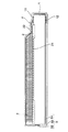
図1は、本発明に係る放射線検出器の一実施形態を示す斜視図であり、図2はその拡大図、図3はその断面図である。この実施形態の放射線検出器100は、セラミック製の基台1上に固体撮像素子2を載置したものである。基台1は、表面に固体撮像素子2を載置して収容する凹部10を有し、凹部10に接する表面には、その一辺に沿って複数の電極パッド11が配列されている。これらの電極パッド11は、基台1の裏面に配置されている外部接続用の電極端子12と基台1を貫通している配線13によって電気的に接続されている。
【0013】
固体撮像素子2は、CCDイメージセンサからなり、光電変換素子21が配列されて受光部を形成している。各光電変換素子21は図示していない信号ラインによって固体撮像素子2の一辺に配置された電極パッド22のうち対応する電極パッド22と電気的に接続されている。固体撮像素子2は基台1上にそれぞれの対応する電極パッド11、22が近接するように載置されており、対応する電極パッド11、22同士は配線4によって電気的に接続されている。
【0014】
固体撮像素子2の受光部上には、入射した放射線を光電変換素子21が感度を有する波長帯の光に変換する柱状構造のシンチレータ3が形成されている。シンチレータ3には、各種の材料を用いることができるが、発光効率が良いTlドープのCsI等が好ましい。
【0015】
さらに、固体撮像素子2と基台1の表面を覆う保護膜5が形成されている。この保護膜5は、X線透過性で、水蒸気を遮断するものであり、基台1側から電気絶縁性の第1の有機膜51、金属薄膜52、電気絶縁性の第2の有機膜53が積層されて構成されている。
【0016】
第1の有機膜51と第2の有機膜53には、ポリパラキシリレン樹脂(スリーボンド社製、商品名パリレン)、特にポリパラクロロキシリレン(同社製、商品名パリレンC)を用いることが好ましい。パリレンによるコーティング膜は、水蒸気及びガスの透過が極めて少なく、撥水性、耐薬品性も高いほか、薄膜でも優れた電気絶縁性を有し、放射線、可視光線に対して透明であるなど有機膜51、53にふさわしい優れた特徴を有している。また、金属薄膜52としては、金、銀、アルミなどの金属薄膜が使用できる。この金属薄膜52はシンチレータ3で発せられた光のうち、固体撮像素子2側でなく、放射線入射面側に向かう光を反射することで検出器の検出感度を増大させるミラーの役目を果たす。
【0017】
電極パッド11、22と配線4部分の保護膜5をさらに覆って包み込むようにして保護樹脂層6が形成されている。この保護樹脂層6としては、保護膜5との接着性が良好な樹脂、例えばアクリル系接着剤である協立化学産業株式会社製WORLD ROCK No.801-SET2(70,000cPタイプ)を用いることが好ましい。
【0018】
次に、図4〜図13を用いて本発明に係る放射線検出器の製造工程を具体的に説明する。最初に図4に示されるような基台1を用意する。この基台1は、裏面に外部接続用の電極端子12を表面に電極パッド11が配列されており、電極パッド11が配列された1辺に隣接する対向する2辺には表面側に突出するガイド部14が形成され、このガイド部14に挟まれた部分に凹部10が形成されている。
【0019】
この凹部10に固体撮像素子2をその電極パッド22が基台1の電極パッド11側を向くようにして光電変換素子21の受光面を表にして載置して図5に示されるように固定する。このときに、ガイド部14を利用して固体撮像素子2の位置決めを行うことで作業が容易となる。そして、電極パッド11と電極パッド22とをワイヤボンディングにより配線4で電気的に接続する(図6、図7参照)。
【0020】
次に、図8、図9に示されるように固体撮像素子2の受光部上にTlをドープしたCsIを真空蒸着法によって厚さ約200μmの柱状結晶として成長させることによりシンチレータ3層を形成する。CsIは、吸湿性が高く、露出したままにしておくと空気中の水蒸気を吸湿して溶解してしまうので、その保護のため、図10に示されるように、CVD(化学的蒸着)法によりシンチレータ3が形成された固体撮像素子2付の基台1全体を厚さ10μmのパリレンで包み込み、第1の有機膜51を形成する。
【0021】
具体的には、金属の真空蒸着と同様に真空中で蒸着によるコーティングを行うもので、原料となるジパラキシリレンモノマーを熱分解して、生成物をトルエン、ベンゼンなどの有機溶媒中で急冷しダイマーと呼ばれるジパラキシリレンを得る工程と、このダイマーを熱分解して、安定したラジカルパラキシリレンガスを生成させる工程と、発生したガスを素材上に吸着、重合させて分子量約50万のポリパラキシリレン膜を重合形成させる工程からなる。
【0022】
CsIの柱状結晶の間には隙間があるが、パリレンはこの狭い隙間にある程度入り込むので、第1の有機膜51は、シンチレータ3層に密着し、シンチレータ3を密封する。また、この第1の有機膜51は、電極パッド11、22の表面のみならず両者を繋ぐ配線4の周囲にも形成され、配線4を被覆する。これにより配線4の接着強度、機械的強度が増すので、その後の工程において配線4の取り扱いが容易になる。このパリレンコーティングにより、凹凸のあるシンチレータ3層表面に均一な厚さの精密薄膜コーティングを形成することができる。また、パリレンのCVD形成は、金属蒸着時よりも真空度が低く、常温で行うことができるため、加工が容易である。
【0023】
続いて、図11に示されるように、第1の有機膜51の入射面側の表面に0.15μm厚さのAl膜を蒸着法により積層することで金属薄膜52を形成する。この金属薄膜52を形成する際には、シンチレータ3層の前に適切なマスク(図示せず)を配置して、シンチレータ3層の直上部分の第1の有機膜51上にのみ金属薄膜52を形成することが望ましい。しかしながら、マスクを配置しても蒸着時には金属蒸気が僅かながらマスクの外側へと回り込んでしまうことがある。このため、特に、受光部と電極パッドとの間隔が狭い場合、金属薄膜52をシンチレータ3層の直上部分だけに形成するのは困難であり、配線4や電極パッド11、22上にまで金属が蒸着されてしまうことがある。本発明によれば、配線4と電極パッド11、22が第1の有機膜51で被覆されているので、金属薄膜52が配線4と電極パッド11、22上に直接形成されることがなく、金属薄膜52による配線4、電極パッド11、22の短絡を効果的に防止できる。
【0024】
また、金属薄膜52の蒸着時、マスクを配置しない場合も、配線4や電極パッド11、22部分にまで金属薄膜52が形成されることになるが、配線4と電極パッド11、22は第1の有機膜51で被覆されているので、短絡は防止されている。また、金属薄膜52を第1の有機膜51を介して配線4と電極パッド11、22を覆う幅広い領域に形成することで、耐湿性をより向上させることができる。
【0025】
そして、再度CVD法により、パリレンを基板全体の表面に10μm厚さで被覆して第2の有機膜53を形成する(図12参照)。この第2の有機膜53は、金属薄膜52のハンドリング等による汚れやはく離、酸化による劣化を防止するためのものである。こうして第1の有機膜51、金属薄膜52、第2の有機膜53を積層させてなる保護膜5が形成される。
【0026】
金属薄膜52を第1の有機膜51を介して配線4や電極パッド11、22上にも形成した場合、金属薄膜52、第2の有機膜53は電極パッド11、22の表面のみならず両者を繋ぐ配線4の周囲にも形成されており、第1の有機膜51と合わせて配線4を三重に被覆していることになり、より配線4の機械的強度、接着強度を上げることができる。また、上述したようにマスクを用いて金属薄膜52を形成した場合は、配線4の周囲や電極パッド11、22上には第1の有機膜51と第2の有機膜53の二重被覆が形成されることになる。
【0027】
続いて、電極パッド11、12の保護膜5上に保護膜5で被覆されている配線4を包み込むように樹脂を塗布して硬化させることで保護樹脂層6を形成する。配線4は、電極パッド11、12を覆う保護膜5上に突出し、その周囲は、配線4上にまで金属薄膜52を形成した場合は、有機膜51、53と金属薄膜52からなる保護膜5により三重に被覆される(図14参照)。また、配線4上には金属薄膜52を形成していない場合には、有機膜51、53により二重に被覆される(図15参照)。いずれの場合も、図13〜図15に示されるように保護樹脂層6が被覆配線4の周囲に回り込み、配線4をポッティングしている。これにより配線4がさらに保護されるので、使用時の配線4の破損を効果的に防止できる。この保護樹脂層6は必ずしも設ける必要はないが、配線4の保護のためには設けることが好ましい。
【0028】
この後で形成した保護膜5のうち基台1の裏面の保護膜5を除去して基台1裏面に設けられている外部接続用の電極端子12を露出させることで図1〜図3に示される放射線検出器が得られる。
【0029】
続いて、本実施形態の動作を図1〜図3により、説明する。入射面側から入射したX線(放射線)は、保護膜5、すなわち、第2の有機膜53、金属薄膜52、第1の有機膜51の全てを透過してシンチレータ3に達する。このX線は、シンチレータ3で吸収され、X線の光量に比例した光が放射される。放射された光のうち、X線の入射方向に逆行した光は、第1の有機膜51を透過して、金属薄膜52で反射される。このため、シンチレータ3で発生した光はほとんど全てが光電変換素子2へと入射する。このため、効率の良い高感度の測定が可能となる。
【0030】
各々の光電変換素子2では、光電変換により、この可視光の光量に対応する電気信号が生成されて一定時間蓄積される。この可視光の光量は入射するX線の光量に対応しているから、つまり、各々の光電変換素子2に蓄積されている電気信号は、入射するX線の光量に対応することになり、X線画像に対応する画像信号が得られる。光電変換素子2に蓄積されたこの画像信号を図示していない信号ラインから電極パッド22、配線4、電極パッド11、配線13を介して最終的には電極端子12から順次出力することにより、外部へと転送し、これを所定の処理回路で処理することにより、X線像を表示することができる。
【0031】
以上の説明では、保護膜5としてパリレン製の有機膜51、53の間に金属薄膜52を挟み込んだ構造のものについて説明したが、第1の有機膜51と第2の有機膜53の材料は異なるものでも良く、金属薄膜52として金等の腐食に強い材料を使用しているような場合は、第2の有機膜53自体を設けなくてもよい。
【0032】
また、ここでは、第1の有機膜51が基台1の側面部までを覆っている形態について説明してきたが、第1の有機膜51は少なくともシンチレータ3全体と電極パッド11、22と配線4を覆っていれば良く、基台1のその他の部分まで覆っている必要はない。ただし、基台1表面まで覆っている場合には、第1の有機膜51の縁部分が基台1に密着することで縁部分からの第1の有機膜51の剥がれを効果的に防止できるため好ましい。
【0033】
さらに、固体撮像素子2は、アモルファスシリコン製のフォトダイオード(PD)アレイと薄膜トランジスタ(TFT)で形成したものでもよいし、MOS型のイメージセンサでもよい。
【0034】
このような構成を採用することにより、放射線検出器の厚みを2.5mm程度と従来良く用いられてきたFOP(ファイバ光学プレート)付の放射線検出器の厚み5.0mmの半分程度に薄くすることが可能となった。また、ボンディングパッドと受光部との間隔を狭くすることで、従来品(特開平10-282243号公報)と同程度の受光部の面積を確保しつつ、受光部周辺の面積を小さくすることで全体の面積を小さくすることができるので、コンパクト化(従来品の約90%)した放射線検出器が実現できる。これは口腔内に挿入して使用する歯科用の放射線検出器においては大きな利点である。
【0035】
【発明の効果】
以上説明したように本発明によれば、固体撮像素子の受光部表面上に形成されているシンチレータと、固体撮像素子とそれを載置する基台双方の電極パッドと、両者を電気的に接続する配線を有機膜で被覆してその上に金属薄膜を形成している。そのため、外部回路との電気的接続用のライン形成が容易になり、作業性が向上する。また、小型の放射線検出素子において、受光部をできるだけ大きく形成することが容易になる。さらに、有機膜がシンチレータを密封することでシンチレータの耐湿性を確保でき、この有機膜が電極パッドと配線をも被覆して保護していることで、配線の断線を効果的に防止できる。有機膜上に形成されている金属薄膜は、シンチレータの耐湿性をさらに向上させるが、この金属薄膜と配線、電極パッドとの間に電気絶縁性の有機膜が介在することで短絡が効果的に防止される。
【図面の簡単な説明】
【図1】本発明に係る放射線検出器の実施形態を示す斜視図である。
【図2】図1の部分拡大図である。
【図3】本発明に係る放射線検出器の実施形態を示す側面図である。
【図4】図1の装置に用いられる基台の斜視図である。
【図5】図1の装置の製造工程を説明する側面図である。
【図6】図5の工程の次の工程を説明する側面図である。
【図7】図6の工程を説明する斜視図である。
【図8】図6の工程の次の工程を説明する側面図である。
【図9】図8の工程を説明する斜視図である。
【図10】図8の工程の次の工程を説明する側面図である。
【図11】図10の工程の次の工程を説明する側面図である。
【図12】図11の工程の次の工程を説明する側面図である。
【図13】図12の工程の次の工程を説明する側面図である。
【図14】図13における配線部分の拡大断面図である。
【図15】別の実施形態における図14に該当する部分の拡大断面図である。
【符号の説明】
1…基台、2…固体撮像素子、3…シンチレータ、4、13…配線、5…保護膜、6…保護樹脂層、10…凹部、11、22…電極パッド、20…基板、21…光電変換素子、51、53…有機膜、52…金属薄膜。[0001]
BACKGROUND OF THE INVENTION
The present invention relates to a radiation detector used for capturing a radiographic image, and more particularly to a small-sized radiation detector for dental use or the like used by being inserted into an oral cavity.
[0002]
[Prior art]
An X-ray image sensor using a CCD instead of an X-ray photosensitive film has been widely used as a medical X-ray diagnostic apparatus. In such a radiation imaging system, two-dimensional image data based on radiation is acquired as an electrical signal using a radiation detection element having a plurality of pixels, and this signal is processed by a processing device and displayed on a monitor. . A typical radiation detection element has a mechanism in which a scintillator is disposed on a photodetector arranged in one or two dimensions, and incident radiation is converted into light by the scintillator and detected.
[0003]
International Publication WO98 / 36291 discloses a radiation detector using CsI as a scintillator material and having a protective film made of parylene or the like for preventing the scintillator from absorbing moisture. In this radiation detector, the bonding pad is exposed from the protective film, and the image signal is read by connecting the bonding pad and external wiring.
[0004]
[Problems to be solved by the invention]
By the way, in a radiation detector that is inserted into the oral cavity for use in dentistry or the like, the entire detector must be reduced in size, while the imaging area needs to be as large as possible. When such a configuration is adopted in such a small radiation detector, if the light receiving part is enlarged, the distance from the bonding pad becomes narrow, and it becomes difficult to form a protective film and connect to external wiring. Workability deteriorates.
[0005]
SUMMARY OF THE INVENTION An object of the present invention is to provide a radiation detector that achieves both a reduction in size and an increase in imaging area, is easy to manufacture, and can ensure durability.
[0006]
In order to solve the above problems, a radiation detector according to the present invention includes (1) a light receiving unit in which a plurality of photoelectric conversion elements are arranged, and an edge of the same surface as the light receiving surface of the light receiving unit. A solid-state imaging device including an electrode pad electrically connected to the device; (2) an external connection electrode portion disposed on one surface side; and the other surface side electrode portion, a base which have the electrode pads are electrically connected, and the solid-state image sensor with placing toward the opposite surface as the light-receiving surface of the solid-state image pickup element on the other surface side of the mounting on the surface A base on which the electrode pads of the base are placed facing each other and fixed; (3) a scintillator formed on the light receiving surface of the solid-state image sensor; and (4) a solid-state image sensor and a base. response and wiring for electrically connecting the electrode pads to each other by wire bonding to, (5) Shin With sealing the regulator, a first organic film electrically insulating is formed to cover the wiring with both of the electrode pads, (6) And a metal thin film formed on the first organic film.
[0007]
In the radiation detector according to the present invention, a solid-state image sensor is mounted and fixed in advance on a base having an electrode portion for external connection, and each electrode pad of the base and the solid-state image sensor is electrically connected by wiring. After the connection, a scintillator is formed on the surface of the light receiving unit of the solid-state imaging device, the surface of the scintillator, the wiring, and both electrode pads are covered with a first organic film, and a metal thin film is formed thereon. Therefore, it is easy to form a line for electrical connection to the outside, and workability is improved. For this reason, in a small radiation detection element, it becomes easy to form a light receiving part as large as possible. Further, since the first organic film seals the scintillator, moisture resistance can be ensured. Further, since the organic film covers and protects the electrode pads and the wiring, the disconnection of the wiring can be effectively prevented. Although the metal thin film formed on the first organic film further improves the moisture resistance, a short circuit is caused by the presence of the electrically insulating first organic film between the metal thin film and the wiring and electrode pads. Is prevented.
[0008]
A second organic film formed on the metal thin film may be further provided. The durability of the protective film is further improved by covering the metal thin film with an organic film.
[0009]
Moreover, you may further provide the protective resin which covers wiring from the 1st organic film or the 2nd organic film . Thereby, the protection from the short circuit and the disconnection of the wiring is further ensured.
[0010]
The first organic film may cover the base surface. The moisture resistance is further ensured by covering the base surface with the first organic film.
[0011]
DETAILED DESCRIPTION OF THE INVENTION
DESCRIPTION OF EXEMPLARY EMBODIMENTS Hereinafter, preferred embodiments of the invention will be described in detail with reference to the accompanying drawings. In order to facilitate the understanding of the description, the same reference numerals are given to the same components in the drawings as much as possible, and duplicate descriptions are omitted. In addition, the dimensions and shapes in each drawing are not necessarily the same as actual ones, and some parts are exaggerated for easy understanding.
[0012]
FIG. 1 is a perspective view showing an embodiment of a radiation detector according to the present invention, FIG. 2 is an enlarged view thereof, and FIG. 3 is a sectional view thereof. In the
[0013]
The solid-
[0014]
A
[0015]
Further, a
[0016]
For the first
[0017]
A
[0018]
Next, the manufacturing process of the radiation detector according to the present invention will be specifically described with reference to FIGS. First, a base 1 as shown in FIG. 4 is prepared. The base 1 has an
[0019]
The solid-
[0020]
Next, as shown in FIG. 8 and FIG. 9, a
[0021]
Specifically, the coating is performed by vapor deposition in the same manner as metal vacuum vapor deposition. The raw material diparaxylylene monomer is thermally decomposed and the product is quenched in an organic solvent such as toluene or benzene. A process for obtaining diparaxylylene called a dimer, a process for thermally decomposing the dimer to generate a stable radical paraxylylene gas, and a gas having a molecular weight of about 500,000 by adsorbing and polymerizing the generated gas on the material. It consists of the process of polymerizing the xylylene film.
[0022]
Although there is a gap between CsI columnar crystals, since parylene enters the narrow gap to some extent, the first
[0023]
Subsequently, as shown in FIG. 11, a metal
[0024]
In addition, when the metal
[0025]
Then, the second
[0026]
When the metal
[0027]
Subsequently, a
[0028]
The
[0029]
Next, the operation of this embodiment will be described with reference to FIGS. X-rays (radiation) incident from the incident surface side pass through all of the
[0030]
In each
[0031]
In the above description, the
[0032]
Here, the first
[0033]
Further, the solid-
[0034]
By adopting such a configuration, the thickness of the radiation detector can be reduced to about 2.5mm, which is about half that of the 5.0mm thickness of the conventional radiation detector with FOP (fiber optical plate). It became. In addition, by reducing the distance between the bonding pad and the light receiving part, the area around the light receiving part can be reduced while securing the same light receiving part area as the conventional product (Japanese Patent Laid-Open No. 10-282243). Since the entire area can be reduced, a compact radiation detector (about 90% of the conventional product) can be realized. This is a great advantage in a dental radiation detector used by being inserted into the oral cavity.
[0035]
【The invention's effect】
As described above, according to the present invention, the scintillator formed on the surface of the light receiving unit of the solid-state image sensor, the electrode pads of both the solid-state image sensor and the base on which the solid-state image sensor is mounted, and the two are electrically connected. The wiring to be covered is covered with an organic film, and a metal thin film is formed thereon. Therefore, it is easy to form a line for electrical connection with an external circuit, and workability is improved. In addition, in a small radiation detection element, it becomes easy to form a light receiving portion as large as possible. Furthermore, the organic film seals the scintillator to ensure the moisture resistance of the scintillator, and the organic film also covers and protects the electrode pads and the wiring, thereby effectively preventing the wiring from being disconnected. The metal thin film formed on the organic film further improves the moisture resistance of the scintillator. However, an electrical insulating organic film is interposed between the metal thin film, the wiring, and the electrode pad, so that a short circuit is effective. Is prevented.
[Brief description of the drawings]
FIG. 1 is a perspective view showing an embodiment of a radiation detector according to the present invention.
FIG. 2 is a partially enlarged view of FIG.
FIG. 3 is a side view showing an embodiment of a radiation detector according to the present invention.
4 is a perspective view of a base used in the apparatus of FIG. 1. FIG.
FIG. 5 is a side view for explaining a manufacturing process of the apparatus of FIG. 1;
6 is a side view for explaining a step subsequent to the step of FIG. 5. FIG.
FIG. 7 is a perspective view illustrating the step of FIG. 6;
FIG. 8 is a side view for explaining the next step of the step of FIG. 6;
FIG. 9 is a perspective view for explaining the step of FIG. 8;
10 is a side view for explaining the next step of the step of FIG. 8. FIG.
11 is a side view for explaining the next step of the step of FIG.
12 is a side view for explaining the next step of the step of FIG. 11. FIG.
FIG. 13 is a side view for explaining the next step of the step of FIG.
14 is an enlarged cross-sectional view of a wiring portion in FIG.
FIG. 15 is an enlarged cross-sectional view of a portion corresponding to FIG. 14 in another embodiment.
[Explanation of symbols]
DESCRIPTION OF SYMBOLS 1 ... Base, 2 ... Solid-state image sensor, 3 ...
Claims (5)
一方の表面側に配置される外部接続用の電極部と、他方の表面側に配置され、前記電極部と電気的に接続されている電極パッドとを有する基台であって、前記固体撮像素子を前記他方の表面側の載置面上に前記受光面と反対の面を向けて載置するとともに前記固体撮像素子と前記基台の各電極パッドを向き合わせて固定している基台と、
前記固体撮像素子の受光部表面上に形成されているシンチレータと、
前記固体撮像素子と前記基台の対応する電極パッド同士をワイヤボンディングにより電気的に接続する配線と、
前記シンチレータを密封するとともに、前記電極パッドの双方と前記配線とを被覆して形成されている電気絶縁性の第1の有機膜と、
前記第1の有機膜上に形成されている金属薄膜と、
を備えている放射線検出器。A solid-state imaging device comprising: a light- receiving unit in which a plurality of photoelectric conversion elements are arranged; and an electrode pad arranged along the edge of the same surface as the light-receiving surface of the light-receiving unit and electrically connected to the photoelectric conversion element; ,
And electrode portions for external connection is disposed on one surface side, it is arranged on the other surface side, a base on which to have a an electrode pad the being the electrode portion electrically connected to, the solid A base on which the element is placed with the surface opposite to the light receiving surface facing the placement surface on the other surface side, and the solid-state imaging device and each electrode pad of the base are fixed facing each other ; ,
A scintillator formed on the light receiving surface of the solid-state imaging device;
And wiring electrically connected by the solid-state imaging device and the corresponding electrode pads to each other the wire bonding of the base,
Sealing the scintillator and electrically insulating first organic film formed so as to cover both the electrode pad and the wiring;
A metal thin film formed on the first organic film;
Radiation detector.
Priority Applications (6)
| Application Number | Priority Date | Filing Date | Title |
|---|---|---|---|
| JP2000148280A JP4234303B2 (en) | 2000-05-19 | 2000-05-19 | Radiation detector |
| AU2001258774A AU2001258774A1 (en) | 2000-05-19 | 2001-05-18 | Radiation detector and method of manufacture thereof |
| EP01932139A EP1300694B1 (en) | 2000-05-19 | 2001-05-18 | Radiation detector and method of manufacture thereof |
| US10/276,726 US7151263B2 (en) | 2000-05-19 | 2001-05-18 | Radiation detector and method of manufacture thereof |
| PCT/JP2001/004172 WO2001088568A1 (en) | 2000-05-19 | 2001-05-18 | Radiation detector and method of manufacture thereof |
| DE60144280T DE60144280D1 (en) | 2000-05-19 | 2001-05-18 | Lung |
Applications Claiming Priority (1)
| Application Number | Priority Date | Filing Date | Title |
|---|---|---|---|
| JP2000148280A JP4234303B2 (en) | 2000-05-19 | 2000-05-19 | Radiation detector |
Publications (2)
| Publication Number | Publication Date |
|---|---|
| JP2001330674A JP2001330674A (en) | 2001-11-30 |
| JP4234303B2 true JP4234303B2 (en) | 2009-03-04 |
Family
ID=18654336
Family Applications (1)
| Application Number | Title | Priority Date | Filing Date |
|---|---|---|---|
| JP2000148280A Expired - Fee Related JP4234303B2 (en) | 2000-05-19 | 2000-05-19 | Radiation detector |
Country Status (1)
| Country | Link |
|---|---|
| JP (1) | JP4234303B2 (en) |
Families Citing this family (5)
| Publication number | Priority date | Publication date | Assignee | Title |
|---|---|---|---|---|
| US7034306B2 (en) | 1998-06-18 | 2006-04-25 | Hamamatsu Photonics K.K. | Scintillator panel and radiation image sensor |
| JP2011058964A (en) * | 2009-09-10 | 2011-03-24 | Toshiba Corp | X-ray plane detector, and method for manufacturing the same |
| JP6226579B2 (en) * | 2013-06-13 | 2017-11-08 | 東芝電子管デバイス株式会社 | Radiation detector and manufacturing method thereof |
| JP7108364B2 (en) * | 2018-09-04 | 2022-07-28 | キヤノン電子管デバイス株式会社 | Radiation detector, radiation detector manufacturing method and apparatus, scintillator panel, scintillator panel manufacturing method and apparatus |
| JP7353191B2 (en) * | 2020-01-14 | 2023-09-29 | キヤノン電子管デバイス株式会社 | Radiation detection module and radiation detector |
-
2000
- 2000-05-19 JP JP2000148280A patent/JP4234303B2/en not_active Expired - Fee Related
Also Published As
| Publication number | Publication date |
|---|---|
| JP2001330674A (en) | 2001-11-30 |
Similar Documents
| Publication | Publication Date | Title |
|---|---|---|
| JP4398065B2 (en) | Radiation detector | |
| CA2261663C (en) | Radiation detection device and method of producing the same | |
| JP4447752B2 (en) | Radiation detector | |
| JP4234304B2 (en) | Radiation detector | |
| JP3077941B2 (en) | Radiation detecting element and method of manufacturing the same | |
| JP4283427B2 (en) | Radiation detector and scintillator panel | |
| JP2000284053A (en) | Radiation detector element | |
| TWI399860B (en) | Radiation photography device | |
| US6940072B2 (en) | Radiation detection device and method of making the same | |
| EP1300694B1 (en) | Radiation detector and method of manufacture thereof | |
| JP4087597B2 (en) | Method for manufacturing X-ray imaging apparatus | |
| JP4234303B2 (en) | Radiation detector | |
| JP4234305B2 (en) | Radiation detector | |
| JP3029873B2 (en) | Radiation detecting element and method of manufacturing the same | |
| JP4440979B2 (en) | X-ray imaging device |
Legal Events
| Date | Code | Title | Description |
|---|---|---|---|
| A621 | Written request for application examination |
Free format text: JAPANESE INTERMEDIATE CODE: A621 Effective date: 20070517 |
|
| A131 | Notification of reasons for refusal |
Free format text: JAPANESE INTERMEDIATE CODE: A131 Effective date: 20080916 |
|
| A521 | Request for written amendment filed |
Free format text: JAPANESE INTERMEDIATE CODE: A523 Effective date: 20081110 |
|
| TRDD | Decision of grant or rejection written | ||
| A01 | Written decision to grant a patent or to grant a registration (utility model) |
Free format text: JAPANESE INTERMEDIATE CODE: A01 Effective date: 20081209 |
|
| A01 | Written decision to grant a patent or to grant a registration (utility model) |
Free format text: JAPANESE INTERMEDIATE CODE: A01 |
|
| A61 | First payment of annual fees (during grant procedure) |
Free format text: JAPANESE INTERMEDIATE CODE: A61 Effective date: 20081211 |
|
| FPAY | Renewal fee payment (event date is renewal date of database) |
Free format text: PAYMENT UNTIL: 20111219 Year of fee payment: 3 |
|
| R150 | Certificate of patent or registration of utility model |
Free format text: JAPANESE INTERMEDIATE CODE: R150 Ref document number: 4234303 Country of ref document: JP Free format text: JAPANESE INTERMEDIATE CODE: R150 |
|
| FPAY | Renewal fee payment (event date is renewal date of database) |
Free format text: PAYMENT UNTIL: 20121219 Year of fee payment: 4 |
|
| FPAY | Renewal fee payment (event date is renewal date of database) |
Free format text: PAYMENT UNTIL: 20131219 Year of fee payment: 5 |
|
| LAPS | Cancellation because of no payment of annual fees |