JP4230468B2 - Inductance element formed on a semiconductor substrate - Google Patents
Inductance element formed on a semiconductor substrate Download PDFInfo
- Publication number
- JP4230468B2 JP4230468B2 JP2005068567A JP2005068567A JP4230468B2 JP 4230468 B2 JP4230468 B2 JP 4230468B2 JP 2005068567 A JP2005068567 A JP 2005068567A JP 2005068567 A JP2005068567 A JP 2005068567A JP 4230468 B2 JP4230468 B2 JP 4230468B2
- Authority
- JP
- Japan
- Prior art keywords
- conductive film
- inductance element
- strip
- substrate
- semiconductor substrate
- Prior art date
- Legal status (The legal status is an assumption and is not a legal conclusion. Google has not performed a legal analysis and makes no representation as to the accuracy of the status listed.)
- Expired - Fee Related
Links
Images


Landscapes
- Coils Or Transformers For Communication (AREA)
- Internal Circuitry In Semiconductor Integrated Circuit Devices (AREA)
- Semiconductor Integrated Circuits (AREA)
Description
本発明は、集積回路を構成する半導体基板上に形成されるインダクタンス素子に関し、特に損失が少なくインダクタンスの低下が少ない構造のインダクタンス素子に関する。 The present invention relates to an inductance element formed on a semiconductor substrate that constitutes an integrated circuit, and more particularly to an inductance element having a structure with low loss and low inductance reduction.
近年において携帯電話等の携帯通信機器の小型化が鋭意進められている。かかる小型携帯通信機器に使用される高周波回路を、シリコン半導体を利用した集積回路で構成する要求が高まってきている。高周波回路は、トランジスタ、抵抗、容量に加えて、コイルやトランスといったインダクタンス素子が必要になる。従って、シリコン半導体基板にトランジスタや抵抗等を利用した集積回路と共に、インダクタンス素子も形成することが必要になる。 In recent years, downsizing of mobile communication devices such as mobile phones has been promoted. There is an increasing demand for configuring a high-frequency circuit used in such a small portable communication device with an integrated circuit using a silicon semiconductor. A high-frequency circuit requires an inductance element such as a coil or a transformer in addition to a transistor, a resistor, and a capacitor. Therefore, it is necessary to form an inductance element on the silicon semiconductor substrate together with an integrated circuit using transistors, resistors, and the like.
かかるインダクタンス素子は、一般的には、半導体基板表面に形成した絶縁膜上に、アルミニウム等の帯状導電膜を渦巻き状にあるいは巻き線状の形成することで実現される。しかしながら、かかる構成では、インダクタンス素子のごく近傍に半導体基板が存在し、インダクタンス素子に電流を流した時に発生する磁束の変化を妨げる渦電流がその半導体基板に発生し、特性に損失が伴うことが知られている。 Such an inductance element is generally realized by forming a strip-like conductive film such as aluminum in a spiral shape or a winding shape on an insulating film formed on the surface of a semiconductor substrate. However, in such a configuration, there is a semiconductor substrate in the immediate vicinity of the inductance element, and an eddy current that prevents a change in magnetic flux generated when a current is passed through the inductance element is generated in the semiconductor substrate, resulting in loss of characteristics. Are known.
即ち、巻き線状に形成された帯状導電層をトランスにおける一次コイルと考えると、不純物を含む半導体基板そのものは抵抗値が低いので高周波領域では短絡された二次コイルのように作用する。この二次コイルの存在による損失は、特に高周波領域において顕著に見られ、そのような半導体基板内の渦電流の発生を防止する為の提案がなされている。例えば、特許文献1には、シリコン半導体基板の表面に複数のPN接合を形成し、その接合に生成される空乏層により、渦電流を抑制することが示されている。即ち、基板表面の渦電流の経路を複数の空乏層により分断し、渦電流を抑制する。あるいは、特許文献2には、シリコン半導体基板の表面に複数のPN接合を形成し、さらにそのPN接合に制御された逆バイアス電圧を印加することで、その接合に形成される空乏層による容量を利用してLC複合回路素子を形成することが提案されている。この公知例においても、基板表面に形成される空乏層により渦電流の発生が抑えられることが示されている。
That is, when the band-shaped conductive layer formed in a winding shape is considered as a primary coil in a transformer, the semiconductor substrate containing impurities itself has a low resistance value, and thus acts like a short-circuited secondary coil in a high-frequency region. The loss due to the presence of the secondary coil is particularly noticeable in the high frequency region, and proposals have been made to prevent the generation of such eddy currents in the semiconductor substrate. For example,
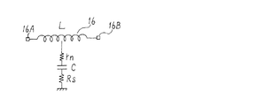
図6は、かかる公知例のインダクタンス素子の構造を示す図である。P型の半導体基板10の表面にN型の不純物領域14が形成され、基板表面に複数のPN接合が形成される。そして、基板10の表面上に形成した絶縁膜12上に、渦巻き状の帯状の導電膜16が形成される。この帯状導電膜16の一端16Aは、図示しない配線に接続され、また、他端16Bは、絶縁膜12内に形成された下層の配線18に接続される。帯状導電膜16の一端から他端に向かって図中の矢印22の方向に電流を流すと、それにより磁束が渦巻き配線内に発生する。
FIG. 6 is a diagram showing the structure of such a known inductance element. An N-
図6に示された構成では、複数のPN接合に空乏層が形成されるので、基板10の表面側に空乏層が多く形成され、帯状導電膜16からなるインダクタンス素子により発生した磁束に対して半導体基板10内に発生する渦電流の流れる抵抗を高くすることができ、渦電流を抑制し上記した渦電流による損失とインダクタンスの低下を防止することができる。
しかしながら、上記の従来例は、半導体基板10の表面に複数の空乏層を形成するだけで、依然として基板表面に渦電流は発生する。また、帯状導電膜の一次コイルと基板内の渦電流の二次コイルとの間には空乏化していない半導体領域が存在するので、両コイル間の相互インダクタンスは低くない。半導体基板の表面領域を全て空乏化することが考えられるが、実際に集積回路が形成されるシリコン半導体基板10の表面に、基板と反対導電型の不純物領域14を形成する場合、微細加工には自ずと限界がある。従って、基板表面が完全に空乏化する程度に複数のPN接合を近接して形成することは困難である。更に、集積回路が形成される半導体基板10はそれ自体高い不純物濃度を有するので、表面に形成されたPN接合間に自然に延びる空乏層の幅はそれほど大きくはならない。その結果、せいぜいPN接合に沿った薄い空乏層が形成されるに止まる。従って、基板表面は完全に空乏化することはなく、上記した通り従来例では、渦電流が発生する領域の抵抗を上げる程度の効果しかない。
However, in the above conventional example, only a plurality of depletion layers are formed on the surface of the
更に、図7の等価回路図に示される通り、基板10の不純物濃度が比較的高く、その基板内の抵抗Rsは比較的低い。また同様に、表面に形成されたN型不純物領域14の抵抗rnも比較的低い。そのため、PN接合により形成された容量Cが、インダクタンス素子Lに電気的につながり、インダクタンス素子の特性に影響を与える。
Furthermore, as shown in the equivalent circuit diagram of FIG. 7, the impurity concentration of the
上記した通り、帯状導電膜16によるインダクタンス素子が一次コイルとなり、基板内の渦電流の経路が二次コイルとなることから、よりインダクタンス素子の損失をなくし特性を良くするためには、両コイル間の絶縁を強くして両コイル間の実効的な相互インダクタンスを低くすることが必要である。
As described above, the inductance element by the strip-like
更に、図5に示された通り、帯状導電膜16に電流22を流すことにより、基板内に加えて、帯状導電膜16自体にも渦電流20が発生する。特に、内側に巻かれた帯状導電膜16には、多くの磁束が発生するので、渦電流20の発生が大きくなる。かかる渦電流もロスの原因となるので、避けることが要求される。その場合、帯状導電膜16の配線幅を狭くすることが考えられるが、配線幅を狭くすると、抵抗が大きくなり更にそれ自体のインダクタンス成分も大きくなり好ましくない。
Further, as shown in FIG. 5, by passing a current 22 through the strip-shaped
そこで、本発明は、半導体基板表面に形成される帯状導電膜によるインダクタンス素子と、半導体基板内の領域との間の絶縁性をより高くした構造のインダクタンス素子を提供することにある。 SUMMARY OF THE INVENTION Accordingly, an object of the present invention is to provide an inductance element having a structure in which insulation between a band-shaped conductive film formed on the surface of a semiconductor substrate and a region in the semiconductor substrate is further increased.
更に、本発明は、半導体基板表面に形成される帯状導電膜自体に発生する渦電流を抑えた構造のインダクタンス素子を提供することにある。 Another object of the present invention is to provide an inductance element having a structure in which eddy currents generated in a strip-like conductive film itself formed on the surface of a semiconductor substrate are suppressed.
上記の目的を達成する為に、第1の本発明は、インダクタンス素子を構成する巻き線状の帯状導電膜の下の半導体基板表面に、複数のPN接合を形成し、そのPN接合に逆バイアス電圧を印加し、基板表面を完全に空乏化する。PN接合に逆バイアスを印加することで、基板表面の不純物濃度が高く隣接するPN接合がある程度離間していても、その空乏層の延びを大きくすることができ、完全に空乏化させることが可能になる。 In order to achieve the above object, according to the first aspect of the present invention, a plurality of PN junctions are formed on the surface of a semiconductor substrate under a winding band-like conductive film constituting an inductance element, and a reverse bias is applied to the PN junctions. A voltage is applied to completely deplete the substrate surface. By applying a reverse bias to the PN junction, even if the impurity concentration on the surface of the substrate is high and adjacent PN junctions are separated to some extent, the extension of the depletion layer can be increased, and it can be completely depleted. become.
更に、上記の目的を達成する為に、第2の発明は、インダクタンス素子を構成する巻き線状の帯状導電膜の下の半導体基板表面に、酸素のイオン注入法により形成される厚い絶縁領域を形成する。この絶縁領域は、通常の集積回路素子領域上に形成される配線用の薄い絶縁膜より大きな膜厚を有する。この厚い絶縁領域の存在により、インダクタンス素子の一次コイルと半導体基板内の渦電流による二次コイルとの間の実効的な相互インダクタンスを小さくすることができる。また、複数のPN接合を利用した完全空乏化する場合よりも、より確実な絶縁が得られるので、インダクタンス素子の損失は少ない。 Furthermore, in order to achieve the above object, the second invention provides a thick insulating region formed by an oxygen ion implantation method on the surface of the semiconductor substrate under the wound strip-shaped conductive film constituting the inductance element. Form. This insulating region has a larger film thickness than a thin insulating film for wiring formed on a normal integrated circuit element region. Due to the presence of the thick insulating region, the effective mutual inductance between the primary coil of the inductance element and the secondary coil due to the eddy current in the semiconductor substrate can be reduced. In addition, since more reliable insulation can be obtained than in the case of complete depletion using a plurality of PN junctions, the loss of the inductance element is small.
更に、上記の目的を達成する為に、第3の発明では、巻き線状に形成される帯状導電膜に、巻き線方向に延びるスリットを形成し、帯状導電膜を巻き線方向に延びる複数の並列配線とする。かかる構成にすることにより、帯状導電膜内に発生する渦電流の経路をなくし、渦電流を抑制して特性損失を抑えることができる。 Furthermore, in order to achieve the above object, in the third invention, a slit extending in the winding direction is formed in the strip-shaped conductive film formed in a winding shape, and a plurality of strips extending in the winding direction are formed in the strip-shaped conductive film. Use parallel wiring. By adopting such a configuration, it is possible to eliminate the path of eddy current generated in the strip-shaped conductive film, suppress eddy current, and suppress characteristic loss.
更に、上記の目的を達成する為に、第4の発明では、巻き線状に形成される帯状導電膜を、巻き線方向の導電率が巻き線方向と垂直方向の導電率よりも高い異方性導電性を有する材料で構成する。例えば、酸化物超電導体や有機導電材料を利用することにより、巻き線方向の導電率が高く、それとは垂直方向の導電率が低い帯状導電膜を形成することができる。かかる材料の場合は、帯状導電膜の巻き線方向の抵抗の増加を防止しつつ内部に発生する渦電流を抑えることができる。 Furthermore, in order to achieve the above object, according to the fourth aspect of the present invention, a strip-shaped conductive film formed in a winding shape is anisotropic in which the conductivity in the winding direction is higher than the conductivity in the direction perpendicular to the winding direction. It is made of a material having conductive conductivity. For example, by using an oxide superconductor or an organic conductive material, it is possible to form a strip-shaped conductive film having high conductivity in the winding direction and low conductivity in the direction perpendicular to the winding direction. In the case of such a material, an eddy current generated inside can be suppressed while preventing an increase in resistance in the winding direction of the belt-like conductive film.
本発明によれば,インダクタンス素子に発生する渦電流を抑えることができる。 According to the present invention, eddy current generated in an inductance element can be suppressed.
以下,図面にしたがって本発明の実施の形態について説明する。但し,本発明の技術的範囲はこれらの実施の形態に限定されず,特許請求の範囲に記載された事項とその均等物まで及ぶものである。 Hereinafter, embodiments of the present invention will be described with reference to the drawings. However, the technical scope of the present invention is not limited to these embodiments, but extends to the matters described in the claims and equivalents thereof.
図1は、実施の形態例のインダクタンス素子の構造図である。この例では、P型の半導体基板10の表面に複数のN型不純物領域14が形成され、表面に複数のPN接合が形成される。更に、半導体基板10の内部には、より濃度の高いN型の埋込み不純物領域30が形成される。この埋め込み不純物領域30は、例えば、高エネルギーイオン注入法により形成することができる。そして、この埋め込み不純物領域30は、N型不純物領域14と同時に形成されるN型の不純物領域32により基板表面に導出される。
FIG. 1 is a structural diagram of an inductance element according to an embodiment. In this example, a plurality of N-
そして、半導体基板10とN型不純物涼気14との間のPN接合に対して、逆バイアス電圧Vが印加される。この逆バイアス電圧Vは、基板表面のPN接合から延びる空乏層がつながる程度の電圧である。
A reverse bias voltage V is applied to the PN junction between the
図2は、図1のインダクタンス素子に逆バイアス電圧を印加した時の詳細断面図である。図中右側に示される不純物濃度分布のように、N型不純物領域14の不純物濃度分布14Nは、基板表面で濃度が低く、基板内部に向かって濃度が高くなる。また、埋込不純物領域30の不純物濃度分布30Nは、図示される通り、N型不純物領域14よりも高い濃度である。
FIG. 2 is a detailed cross-sectional view when a reverse bias voltage is applied to the inductance element of FIG. Like the impurity concentration distribution shown on the right side of the figure, the
そして、基板10の表面領域でのPN接合間に印加される逆バイアス電圧Vは、基板表面の導電層33から、N型不純物領域32、N型の埋込不純物領域30を介してインダクタンス素子の下のPN接合を形成するN型不純物領域14に印加される。従って、そのPN接合から延びる空乏層は、破線に示した様に拡がる。即ち、基板10の表面側での空乏層の延びは大きく、隣接するPN接合から延びる空乏層がつながり、基板表面は完全に空乏化する。また、不純物濃度が高い基板内部のPN接合から拡がる空乏層の延びは、基板表面に比較して少ない。従って、基板内部の埋込不純物領域30から印加される電圧は、不純物領域14の垂直方向の非空乏領域(N型半導体領域)を介して、基板表面に有効に印加され、基板表面の完全空乏化が可能になる。
The reverse bias voltage V applied between the PN junctions in the surface region of the
図1の例では、P型半導体基板10の表面には、平面図で複数本のN型不純物領域14が形成されるが、本発明はかかる形状に限定されず、例えば、平面図で格子状あるいは微小領域をマトリクス状に配置した形状であっても良い。基板表面において、より多くのPN接合が終端する構造であれば、そのPN接合から延びる空乏層により基板表面が完全に空乏化しやすくなる。
In the example of FIG. 1, a plurality of N-
本実施の形態例では、インダクタンス素子を構成する巻き線状の帯状導電膜16が、上記のPN接合が形成された領域上の絶縁膜12上に形成される。この帯状導電膜16は、図1に示される通り、巻き線方向に延びるスリット34を有する。従って、帯状導電膜16は、巻き線方向に延びる複数の並列接続された配線構造となる。
In the present embodiment, the wound belt-like
帯状導電膜16内にスリット34を形成することにより、帯状導電膜16の両端16A,16B間に電流を流した場合でも、帯状導電膜16内に発生する渦電流を少なくすることができる。インダクタンス素子を構成する帯状導電膜16は、それ自体がインダクタンス成分を持たない様にある程度の幅をもつ必要がある。しかしながら、その線幅が大きすぎると、特に巻き線状の内周部分では、多くの磁束が貫通し、それに対する渦電流が帯状導電膜16内に発生する。そこで、本実施の形態例では、その帯状導電膜16内にスリット34を形成し、その渦電流を抑える。帯状導電膜16の幅方向の渦電流の流れる経路がなくなり、その分発生する渦電流はより小さい領域のみとなる。また、スリット34を形成しても、帯状導電膜16は並列接続されているので巻き線方向の抵抗が低くなることはない。
By forming the
このスリット43は、巻き線状の帯状導電膜16の内周の巻き線部分にのみ形成しても有効である。巻き線の外周よりも内周の部分でより多くの磁束が貫通するので、その部分の帯状導電膜16にスリットを形成するだけでも、有効に渦電流を抑制することができる。
It is effective to form the
図3は、別の実施の形態例のインダクタンス素子の断面図である。図3には、インダクタンス素子を構成する帯状導電膜16と、集積回路を構成するMOSトランジスタ42とが示される。通常のMOSトランジスタ42は、P型基板の表面に形成したN型ソース・ドレイン領域43と、ゲート酸化膜上に形成したゲート電極44と、基板表面に形成された絶縁膜12上に導出される配線層45等で構成される。かかる絶縁膜12は、例えばCVD法等により形成されるシリコン酸化膜であるが、その膜厚は全体でせいぜい5000オングストローム程度である。
FIG. 3 is a cross-sectional view of an inductance element according to another embodiment. FIG. 3 shows a strip-like
それに対して、インダクタンス素子を構成する帯状導電膜16が形成される領域の下には、基板10の表面から内部に厚い絶縁領域40が形成される。この絶縁領域40は、例えばサイモックス法と呼ばれる半導体基板上にSOI(Silicon on Insulator) 構造を形成する場合に利用される方法により形成される。即ち、このサイモックス法によれば、基板表面に酸素イオンを注入することにより、半導体シリコン基板の表面から内部へ延びる厚い領域を酸化シリコン領域40に変えることができる。従って、この絶縁領域40は、例えばその膜厚が10000オングストローム以上あり、通常の集積回路素子上の配線用の絶縁膜12の膜厚よりもかなり厚くすることができる。
On the other hand, a thick
この様に、インダクタンス素子を構成する帯状導電膜16の下に、配線用の絶縁膜12 に加えて、基板10の表面から内部へ延びる厚い絶縁領域40を形成することにより、帯状導電膜16とその直下の基板内部の半導体領域との間が完全に絶縁される。また、その距離も大きくなり、帯状導電膜16による一次コイルと基板内部に発生する渦電流による二次コイルとの間の相互インダクタンスを小さくすることができる。また、基板内の渦電流の発生自体も抑制される。
In this way, by forming the thick
図4は、図3のインダクタンス素子の一部断面斜視図である。図4に示される通り、帯状導電膜16の下には、厚い絶縁領域40が形成される。更に、図4の帯状導電膜16の巻き線の内周部分には、複数のスリット34が形成される。帯状導電膜16に電流が流れることにより発生する磁束密度がより高い巻き線の内周部分に、複数のスリット34を設けることにより、帯状導電膜16内に発生する渦電流をより効率的に抑えることができる。
4 is a partial cross-sectional perspective view of the inductance element of FIG. As shown in FIG. 4, a thick
図5は、更に別のインダクタンス素子の構造を示す平面図である。この例は、インダクタンス素子を構成する帯状導電膜内に発生する渦電流を抑える為に、その帯状導電膜を、巻き線方向の導電率がその垂直方向の導電率よりも大きい異方性の導電率をもつ材料により形成する。かかる材料は、例えば、セラミック系の酸化物超電導体である、Y2 Ba4 Cu7 O15やLaBa2 Cu3 O7 等である。或いは、別の材料として、ポリアセチレン等の有機導電材料である。これらの材料は、例えば、スパッタリング法や反応性蒸着法によりこれらの材料の薄膜を形成した後に、化学的エッチングやイオンエッチング法により任意の形状に加工するなどの方法により形成することで、一定方向の導電率がそれに垂直な方向の導電率よりも大きくなるようにすることができる。 FIG. 5 is a plan view showing the structure of still another inductance element. In this example, in order to suppress the eddy current generated in the strip-shaped conductive film constituting the inductance element, the strip-shaped conductive film is made to have an anisotropic conductivity in which the conductivity in the winding direction is larger than the conductivity in the vertical direction. It is made of a material with a rate. Such a material is, for example, Y 2 Ba 4 Cu 7 O 15 or LaBa 2 Cu 3 O 7 which is a ceramic oxide superconductor. Alternatively, another material is an organic conductive material such as polyacetylene. These materials are formed in a certain direction by, for example, forming a thin film of these materials by a sputtering method or a reactive vapor deposition method and then processing them into an arbitrary shape by a chemical etching or an ion etching method. Can be made larger than the conductivity in the direction perpendicular thereto.
図5に示された例では、巻き線状の帯状導電膜を、図中の水平方向の下層配線161,163,165,167と、図中の垂直方向の上層配線160,162,164,166とで構成する。上記した方法により、先ず下層配線用の異方性導電材料層を形成し、図中の横方向のパターンにエッチングして、下層配線161,163,165,167を形成する。更に、その上に絶縁層を形成し上層と下層を接続するビア・ホールを形成し、さらに上層配線用の異方性導電材料層を形成し、図中の縦方向のパターンにエッチングして、上層配線160,162,164,166を形成する。その結果、一端16Aから他端16Bまでの巻き線状の帯状導電膜が形成される。
In the example shown in FIG. 5, the wound belt-like conductive film is made up of the
下層配線161,163,165,167は、図中の矢印(図中水平方向)で示される巻き線方向の導電率が、それに垂直な方向の導電率よりも高い。また同様に、上層配線160,162,164,166は、図中の矢印(図中垂直方向)で示される巻き線方向の導電率が、それに垂直な方向の導電率よりも高い。従って、図5のインダクタンスの帯状導電膜は、その巻き線方向の導電性を犠牲にすることなく、それ自身に発生する渦電流を抑制することができる。
The
以上説明した通り、本発明によれば、半導体基板上に形成されるインダクタンス素子において、インダクタンス素子を構成する帯状導電膜の下の基板表面に複数のPN接合を形成し、そのPN接合に逆バイアス電圧を印加して、基板表面が完全に空乏化するようにしたので、基板表面で発生する渦電流を抑えることができる。更に、基板表面の帯状導電膜による一次コイルと基板内部に発生する渦電流による二次コイルとの間の相互インダクタンスを低くすることができる。従って、インダクタンス素子の特性の損失を少なくすることができる。 As described above, according to the present invention, in the inductance element formed on the semiconductor substrate, a plurality of PN junctions are formed on the substrate surface under the strip-like conductive film constituting the inductance element, and the reverse bias is applied to the PN junction. Since a voltage is applied so that the substrate surface is completely depleted, eddy currents generated on the substrate surface can be suppressed. Furthermore, it is possible to reduce the mutual inductance between the primary coil due to the strip-like conductive film on the substrate surface and the secondary coil due to the eddy current generated inside the substrate. Therefore, the loss of the characteristic of the inductance element can be reduced.
また、本発明によれば、半導体基板上に形成されるインダクタンス素子において、インダクタンスを構成する帯状導電膜の下の基板表面内部に分厚い絶縁領域を形成したので、基板内に発生する渦電流を抑えることができる。また、その厚い絶縁領域により、基板表面の帯状導電膜による一次コイルと基板内部に発生する渦電流による二次コイルとの間の相互インダクタンスを低くすることができる。従って、インダクタンス素子の特性の損失を少なくすることができる。 According to the present invention, in the inductance element formed on the semiconductor substrate, a thick insulating region is formed inside the substrate surface under the strip-shaped conductive film constituting the inductance, so that eddy currents generated in the substrate are suppressed. be able to. In addition, due to the thick insulating region, the mutual inductance between the primary coil due to the strip-like conductive film on the substrate surface and the secondary coil due to the eddy current generated inside the substrate can be reduced. Therefore, the loss of the characteristic of the inductance element can be reduced.
また、本発明によれば、半導体基板上に形成されるインダクタンス素子において、インダクタンスを構成する帯状導電膜にスリットを形成したので、その帯状導電膜自体に発生する渦電流を抑えることができる。従って、インダクタンス素子の特性の損失を少なくすることができる。 According to the present invention, in the inductance element formed on the semiconductor substrate, since the slit is formed in the strip-shaped conductive film constituting the inductance, the eddy current generated in the strip-shaped conductive film itself can be suppressed. Therefore, the loss of the characteristic of the inductance element can be reduced.
更に、本発明によれば、半導体基板上に形成されるインダクタンス素子において、インダクタンスを構成する帯状導電膜を、巻き線方向の導電率がそれと垂直方向の導電率より高い異方性導電率を有する材料で構成されるので、帯状導電膜自体に発生する渦電流を抑えることができる。従って、インダクタンス素子の特性の損失を少なくすることができる。 Furthermore, according to the present invention, in the inductance element formed on the semiconductor substrate, the strip-shaped conductive film constituting the inductance has an anisotropic conductivity in which the conductivity in the winding direction is higher than the conductivity in the direction perpendicular thereto. Since it is made of a material, eddy currents generated in the strip-shaped conductive film itself can be suppressed. Therefore, the loss of the characteristic of the inductance element can be reduced.
10 P型の半導体基板
12 配線用の絶縁膜
14 N型の不純物領域
16 巻き線状の帯状導電膜
20 渦電流
30 N型の埋込不純物領域
32 N型の不純物領域
34 スリット
40 厚い絶縁領域
160〜167 異方性導電率をもつ配線膜
10 P-
Claims (2)
前記半導体基板の表面に形成された絶縁膜と、
前記絶縁膜上に形成され、前記インダクタンス素子を構成する巻き線状の帯状導電膜とを有し、
前記帯状導電膜は、前記巻き線方向の導電率が巻き線方向と垂直方向の導電率よりも高い導電異方性を有する材料で形成されることを特徴とするインダクタンス素子。 In an inductance element formed on a semiconductor substrate,
An insulating film formed on the surface of the semiconductor substrate;
A wound belt-shaped conductive film formed on the insulating film and constituting the inductance element;
The inductance element according to claim 1, wherein the strip-shaped conductive film is formed of a material having a conductivity anisotropy higher in conductivity in the winding direction than in a direction perpendicular to the winding direction.
Priority Applications (1)
| Application Number | Priority Date | Filing Date | Title |
|---|---|---|---|
| JP2005068567A JP4230468B2 (en) | 2005-03-11 | 2005-03-11 | Inductance element formed on a semiconductor substrate |
Applications Claiming Priority (1)
| Application Number | Priority Date | Filing Date | Title |
|---|---|---|---|
| JP2005068567A JP4230468B2 (en) | 2005-03-11 | 2005-03-11 | Inductance element formed on a semiconductor substrate |
Related Parent Applications (1)
| Application Number | Title | Priority Date | Filing Date |
|---|---|---|---|
| JP05962098A Division JP3942264B2 (en) | 1998-03-11 | 1998-03-11 | Inductance element formed on a semiconductor substrate |
Publications (2)
| Publication Number | Publication Date |
|---|---|
| JP2005252272A JP2005252272A (en) | 2005-09-15 |
| JP4230468B2 true JP4230468B2 (en) | 2009-02-25 |
Family
ID=35032403
Family Applications (1)
| Application Number | Title | Priority Date | Filing Date |
|---|---|---|---|
| JP2005068567A Expired - Fee Related JP4230468B2 (en) | 2005-03-11 | 2005-03-11 | Inductance element formed on a semiconductor substrate |
Country Status (1)
| Country | Link |
|---|---|
| JP (1) | JP4230468B2 (en) |
Families Citing this family (4)
| Publication number | Priority date | Publication date | Assignee | Title |
|---|---|---|---|---|
| JP5113554B2 (en) * | 2008-02-26 | 2013-01-09 | パナソニック株式会社 | Planar coil, electric device using the same, power supply device, non-contact power transmission system |
| JP5252486B2 (en) | 2008-05-14 | 2013-07-31 | 学校法人慶應義塾 | Inductor element, integrated circuit device, and three-dimensional mounting circuit device |
| JP5395458B2 (en) * | 2009-02-25 | 2014-01-22 | 学校法人慶應義塾 | Inductor element and integrated circuit device |
| CN213124016U (en) | 2018-03-28 | 2021-05-04 | 株式会社村田制作所 | Resin multilayer substrate and actuator |
-
2005
- 2005-03-11 JP JP2005068567A patent/JP4230468B2/en not_active Expired - Fee Related
Also Published As
| Publication number | Publication date |
|---|---|
| JP2005252272A (en) | 2005-09-15 |
Similar Documents
| Publication | Publication Date | Title |
|---|---|---|
| JP3942264B2 (en) | Inductance element formed on a semiconductor substrate | |
| US9443843B2 (en) | Integrated circuit device | |
| US8232623B2 (en) | Semiconductor device | |
| TWI540725B (en) | Semiconductor device and method of manufacturing the same | |
| US9390983B1 (en) | Semiconductor device and method for fabricating the same | |
| US9299601B2 (en) | SOI RF device and method for forming the same | |
| KR20240132108A (en) | Semiconductor device and method for manufacturing same | |
| US8598651B2 (en) | Semiconductor device with transistor having gate insulating film with various thicknesses and manufacturing method thereof | |
| JP5159365B2 (en) | Semiconductor device and manufacturing method thereof | |
| US20140110814A1 (en) | Resurf High Voltage Diode | |
| US6849913B2 (en) | Integrated circuit including an inductor, active layers with isolation dielectrics, and multiple insulation layers | |
| JP4230468B2 (en) | Inductance element formed on a semiconductor substrate | |
| WO2014050422A1 (en) | Chip diode and method for manufacturing same | |
| US20180026115A1 (en) | Transistor with contacted deep well region | |
| US8362562B2 (en) | Semiconductor device with selected transistor properties | |
| JP2007005835A (en) | Inductance element formed in semiconductor substrate shape | |
| JP2009252965A (en) | Semiconductor device | |
| JP6084357B2 (en) | Semiconductor device | |
| WO2018163605A1 (en) | Semiconductor device and method for manufacturing semiconductor device | |
| JP2019530210A (en) | Improving device performance using backside metallization in the layer transfer process | |
| US20110049584A1 (en) | Semiconductor device | |
| JP2012227489A (en) | Semiconductor device and method of manufacturing the same | |
| JP2009059894A (en) | Semiconductor device | |
| US20170179295A1 (en) | Semiconductor structure | |
| TW201240062A (en) | Self detection device for high voltage ESD protection and manufacturing method for the same |
Legal Events
| Date | Code | Title | Description |
|---|---|---|---|
| A711 | Notification of change in applicant |
Free format text: JAPANESE INTERMEDIATE CODE: A712 Effective date: 20080731 |
|
| A131 | Notification of reasons for refusal |
Free format text: JAPANESE INTERMEDIATE CODE: A131 Effective date: 20080924 |
|
| A521 | Written amendment |
Free format text: JAPANESE INTERMEDIATE CODE: A523 Effective date: 20081107 |
|
| TRDD | Decision of grant or rejection written | ||
| A01 | Written decision to grant a patent or to grant a registration (utility model) |
Free format text: JAPANESE INTERMEDIATE CODE: A01 Effective date: 20081202 |
|
| A01 | Written decision to grant a patent or to grant a registration (utility model) |
Free format text: JAPANESE INTERMEDIATE CODE: A01 |
|
| A61 | First payment of annual fees (during grant procedure) |
Free format text: JAPANESE INTERMEDIATE CODE: A61 Effective date: 20081203 |
|
| R150 | Certificate of patent or registration of utility model |
Free format text: JAPANESE INTERMEDIATE CODE: R150 |
|
| FPAY | Renewal fee payment (event date is renewal date of database) |
Free format text: PAYMENT UNTIL: 20111212 Year of fee payment: 3 |
|
| FPAY | Renewal fee payment (event date is renewal date of database) |
Free format text: PAYMENT UNTIL: 20111212 Year of fee payment: 3 |
|
| S531 | Written request for registration of change of domicile |
Free format text: JAPANESE INTERMEDIATE CODE: R313531 |
|
| S533 | Written request for registration of change of name |
Free format text: JAPANESE INTERMEDIATE CODE: R313533 |
|
| FPAY | Renewal fee payment (event date is renewal date of database) |
Free format text: PAYMENT UNTIL: 20111212 Year of fee payment: 3 |
|
| R350 | Written notification of registration of transfer |
Free format text: JAPANESE INTERMEDIATE CODE: R350 |
|
| FPAY | Renewal fee payment (event date is renewal date of database) |
Free format text: PAYMENT UNTIL: 20111212 Year of fee payment: 3 |
|
| FPAY | Renewal fee payment (event date is renewal date of database) |
Free format text: PAYMENT UNTIL: 20121212 Year of fee payment: 4 |
|
| FPAY | Renewal fee payment (event date is renewal date of database) |
Free format text: PAYMENT UNTIL: 20121212 Year of fee payment: 4 |
|
| FPAY | Renewal fee payment (event date is renewal date of database) |
Free format text: PAYMENT UNTIL: 20131212 Year of fee payment: 5 |
|
| S111 | Request for change of ownership or part of ownership |
Free format text: JAPANESE INTERMEDIATE CODE: R313111 |
|
| R350 | Written notification of registration of transfer |
Free format text: JAPANESE INTERMEDIATE CODE: R350 |
|
| LAPS | Cancellation because of no payment of annual fees |