JP4215424B2 - Manufacturing method of membrane sensor array and membrane sensor array - Google Patents
Manufacturing method of membrane sensor array and membrane sensor array Download PDFInfo
- Publication number
- JP4215424B2 JP4215424B2 JP2001355118A JP2001355118A JP4215424B2 JP 4215424 B2 JP4215424 B2 JP 4215424B2 JP 2001355118 A JP2001355118 A JP 2001355118A JP 2001355118 A JP2001355118 A JP 2001355118A JP 4215424 B2 JP4215424 B2 JP 4215424B2
- Authority
- JP
- Japan
- Prior art keywords
- membrane
- web
- semiconductor material
- sensor array
- region
- Prior art date
- Legal status (The legal status is an assumption and is not a legal conclusion. Google has not performed a legal analysis and makes no representation as to the accuracy of the status listed.)
- Expired - Fee Related
Links
Images


Landscapes
- Micromachines (AREA)
Description
【0001】
【発明の属する技術分野】
本発明は、請求項1または5の上位概念に記載のメンブランセンサーアレーの製造方法および請求項6の上位概念に記載のメンブランセンサーアレーに関する。
【0002】
【従来の技術】
半導体材料支持体を有し、該支持体上にセンサー層の支持体として少なくとも1個の平坦なメンブラン領域が配置されているメンブランセンサーの製造方法はすでに公知となっている。メンブランセンサーアレーが複数の平坦なメンブラン領域を有する場合は、このメンブラン領域は、メンブランおよびウェブの横方向の周囲部分に比較して明らかに改良された熱伝導性を有する材料からなるウェブにより規則的に互いに断熱されている。
【0003】
現在市販されているメンブランセンサーは多くの場合に薄膜として実現されている。このために支持体基板上に数10nmから数μmの厚さの層系を析出し、その後自立するメンブラン領域を得るために、支持体基板を決められた領域で除去する。引き続きメンブランの中心に、例えばメンブランの自立する配置により、包囲する支持体基板から断熱されているセンサー素子を配置し、これは温度センサーおよび流量センサーに好ましい。
【0004】
メンブランを露出するために、2つの方法に分類することができる。
【0005】
1.一般にメンブランを析出する前に、支持体基板の表面に被覆される犠牲層を使用する表面マイクロメカニック(OMM)。犠牲層は後でセンサーの表面からメンブラン中の溶解開口により除去し、これにより自立する構造が生じる。この表面マイクロメカニック法は分離した犠牲層が必要であることにより比較的経費がかかる。
【0006】
2.支持体基板の裏面からエッチング工程によりメンブランを露出する、すなわち、例えば全部の厚さのウェハを通過して開口をエッチングすることによる、バルクマイクロメカニック。
【0007】
多くの使用のためにセンサーアレー(配列)が必要である。このために複数の同じセンサーを線状に並列してまたは二次元的に配置する。温度センサーを使用する場合は、測定信号の空間的分解を可能にするために、これは放熱体により互いに分離しなければならない。
【0008】
放熱体を製造するために、種々の可能性が存在する。良好な熱伝導性材料からなる層をメンブランの表面に析出し、構造化し、良好な熱伝導性材料の残りの構造を放熱体として用いる。
【0009】
しかしながらメンブランを、バルクマイクロメカニック工程を用いて、個々のメンブラン領域の間にバルク材料からなるウェブが残留するように、露出することもできる。バルクマイクロメカニックメンブランセンサーの場合は、一般に裏面のメンブランを異方性エッチング法で、例えばKOH(水酸化カリウム)を用いて露出する。この場合にエッチングは、その異方性にもかかわらず、基板の裏面に、本来のメンブラン構造に必要であるよりかなり多くの場所を必要とする。これによりこの方法では集積密度が制限される。
【0010】
【発明が解決しようとする課題】
本発明の課題は、メンブランセンサーアレーの製造費用を減少し、特に改良された集積密度を有するメンブランセンサーアレーを提供することであり、これは同様に製造費用の減少を可能にする。
【0011】
【課題を解決するための手段】
前記課題は、請求項1または5記載の方法および請求項6記載のメンブランセンサーにより解決される。
【0012】
本発明は、まず半導体材料支持体上にセンサー素子の支持体層として複数の平坦なメンブラン領域が配置され、平坦なメンブラン領域が、メンブラン領域およびウェブの横方向の周囲部分と比較して明らかに改良された熱伝導性を有する材料からなるウェブにより互いに断熱されている、半導体材料支持体を有するメンブランセンサーアレーの製造方法から出発する。メンブラン領域の語は、本発明の範囲で、自立する層だけでなく、最も簡単な場合はウェブより熱伝導性が低い容積部分に配置される1個の層であると理解される。本発明の核心は、半導体材料支持体に、断熱のためにウェブが形成されている位置で、多孔質半導体材料を形成させる次の工程のためのマスキングを維持し、マスキングにより保護されない半導体材料を多孔質化し、その上に、例えば半導体材料支持体もしくは多孔質化した位置に連続するメンブラン層を被覆することにより、メンブラン領域を製造することにある。この方法により、個々のセンサーが十分な程度で断熱されている、メンブランセンサーアレーの高い集積密度を達成することが可能である。この場合に多孔質の半導体材料の製造を、適当なマスキングにより比較的微細な構造で行うことができるという知見を利用する。これにより、それに応じて密に並列に配置することができる、相当する微細なウェブを製造することができ、これは全体としてアレーのセンサーの高い密度を可能にする。断熱は、残りの半導体ウェブが、多孔質の半導体材料に比較して、または以下に詳しく記載するように、除去され、かつ多孔質化した半導体材料により、その際生じる、場合によりガス充填口を有する中空に比較して、明らかに高い熱伝導性を有することにより得られる。
【0013】
本発明の特に有利な実施態様において、マスキングのために、多孔質化した半導体材料を製造する際に安定した層、例えば酸化珪素、窒化珪素または炭化珪素もしくはこれらの組合せ物を使用する場合が有利である。これは更にマスキング層を除去した後にアンダーエッチング工程にもとづきウェブの形の放熱体を、突出する領域なしに実現することができる、マスキングの比較的簡単な可能性である。しかしながらこの方法では自立するウェブを形成することは不可能である。すなわちウェブは常に半導体材料支持体のバルク材料と結合したままてある。
【0014】
決められた幅および高さを有する自立するウェブの形の放熱体を製造するために、更に半導体材料支持体に、断熱のためにウェブが形成される位置で、マスキングとして所定の深さを有する適当なドーピング部を維持し、ドーピング部により割り付けられなかった半導体材料をウェブの周囲部分で多孔質化することが提案される。
【0015】
有利には多孔質化した半導体領域を、メンブラン領域を被覆した後にエッチングにより除去する。このやり方で、連続する槽中のウェブを包囲する半導体領域を多孔質化する場合に、特に自立するウェブ構造が形成される。自立するウェブは、好ましい断熱に十分である放熱体を提供するために十分である。この場合にこの方法は、付加的な犠牲層も、他の、例えば放熱体を形成する金属層も必要でないという利点を有する。むしろメンブラン領域の下側のメンブランセンサーアレーの土台は、例えば連続するメンブラン層の形で、完全に支持体の半導体材料から形成することができる。
【0016】
多孔質シリコンを製造する自体公知の方法の場合は、一般にフッ化水素酸と珪素の電気化学的反応を利用し、この場合に珪素中にスポンジ状の構造を生じる。このためにシリコン半導体支持体(一般にシリコンウェハ)は、フッ化水素酸電解質に対して陽極に接続されていなければならない。例えばフッ化水素酸/エタノールからなる混合物中のシリコンの電気化学的エッチング(陽極化)により、前記深さに部分的にエッチングすることにより多孔質シリコンが生じる。シリコンのエッチングのために、シリコンと電解質の境界面に欠陥電子(ホール)が必要であり、これは流動する電流により供給される。電流密度が臨界電流密度jKRITより小さい場合は、表面に存在するくぼみで印加された電界によりホールが拡散し、ここで有利なエッチングが行われる。例えばp−ドーピングシリコンの場合は、量子効果によりホールがこの領域にもはや浸入できず、エッチング工程が停止するまで、くぼみの間の領域を最小の厚さまで横方向にエッチングする。このやり方で珪素および自由エッチングしたホールからなるスポンジ状の骨格構造が生じる。骨格構造を形成する際にエッチング工程を、ホール先端の領域にのみ行うので、すでにエッチングしたシリコンのスポンジ構造が維持される。これによりすでにエッチングした領域の孔径がほぼ変化せず残る。孔径はフッ化水素酸中のHF濃度、ドーピングおよび電流密度に依存し、数ナノメートルから数10ナノメートルであってもよい。同様に気孔率を約10%から90%以上の範囲に調節できる。
【0017】
多孔質シリコンを製造するために、種々のドーピング基板を使用することができる。一般に種々のドーピング程度のp−ドーピングウェハを使用する。ドーピングにより多孔質シリコン内部で構造の大きさを決定することができる。
【0018】
多孔質構造を形成することにより、シリコンは大きな内部表面およびこれにより包囲するバルクシリコンのような他の化学的および物理的特性(例えば他のエッチング速度、熱伝導性、熱容量等)を取得する。従って反応性が明らかに向上し、これによりバルクシリコンに対する多孔質シリコンの選択的エッチングが可能である。
【0019】
この場合にシリコン中のウェブの製造は以下のように実施する。
【0020】
シリコンの場合は、特にp−ドーピングシリコンおよびn−ドーピングシリコンが著しく異なるエッチング特性を有するという知見を利用することができる。p-ドーピングシリコン中に多孔質シリコンを製造することができる条件下では、これはn−ドーピングシリコン中では不可能であるかまたはきわめて少ない範囲でのみ可能である。従ってマスキング層として、例えばp−ドーピング基板の表面の薄い層を再度n−ドーピングすることができる(イオン注入または拡散により)。電気化学的エッチングの場合にはp−ドーピング領域でのみ多孔質シリコンが生じる。マスキング層の厚さは処理パラメータ(ドーピング量、注入エネルギー、ドーピング物質の後での打ち込み)により変動することができる。多孔質シリコンの形成は等方性工程であるので、それに応じてマスクをアンダーエッチングする。ドーピングにより特徴づけられるウェブ領域を完全にアンダーエッチングする場合は、多孔質シリコンを除去した後に自立するウェブ構造が生じる。
【0021】
多孔質半導体材料のエッチングのために、シリコンの場合は、特にセンサー層を析出した後に実質的に2つの可能性が存在する。1つは強度に希釈した水酸化カリウム溶液(KOH)を使用し、1つはフッ化水素酸(HF)を使用する。この場合に多孔質シリコンを、メンブラン領域を被覆する前になお酸化工程で処理する。
【0022】
本発明のもう1つの有利な実施態様において、半導体材料支持体上にセンサー素子の支持体層として複数の平坦なメンブラン領域が配置され、複数の平坦なメンブラン領域が、メンブラン領域およびウェブの横方向の周囲部分と比較して明らかに改良された熱伝導性を有する材料からなるウェブにより断熱されている、半導体材料支持体を有するメンブランセンサーアレーの製造方法において、半導体材料の前面上に、有利には半導体材料支持体上に、直接メンブラン層を被覆させ、半導体中に少なくともほぼ垂直なエッチング側面を実現させることができる、引き続く異方性プラズマエッチング工程によりウェブを、半導体材料支持体の裏面から形成させることが有利である。この方法により、バルクマイクロメカニック法を使用するにもかかわらず、かなりの程度で、特にメンブランセンサーアレーに関する集積密度の改良を達成することができる。
【0023】
更に本発明は、半導体材料からなる支持体を有し、該支持体上に並列に存在する平坦なメンブラン領域がセンサー素子の支持体層として配置され、このメンブラン領域が、メンブラン領域およびウェブの横方向の周囲部分と比較して明らかに改良された熱伝導性を有する材料からなるウェブにより互いに断熱され、ウェブが支持体の半導体材料から形成されているメンブランセンサーアレーから出発する。本発明のこの構成の中心的思想は、メンブラン領域に直接接触するウェブの幅が50μm未満であることにある。この思想の基礎となる認識は、例えばウェブが連続するメンブランの下側に配置され、メンブランがメンブラン領域に分かれている場合に、この種の形成されたウェブが十分な程度で放熱体の機能を満たすことにある。
【0024】
メンブランセンサーアレーの簡単な構造を得るために、更にウェブが支持体の半導体材料からのみ形成されていることが提案される。
【0025】
例えばシリコンウェハの場合に、ウェブを製造するために、p−ドーピングウェハをドーピングすることによりマスキングを使用する場合は、ウェブ幅およびウェブ厚さをドーピング工程により簡単に調節することができ、これにより熱伝導値を感度よい方法で制御することができる。まさにこのマスキング工程により、垂直方向で見て薄いウェブを製造することができ、これが放熱体の要求を満たす。30μm未満のウェブの厚さがすでに十分であることが判明した。
【0026】
放熱体の構造は、有利にはウェブ、例えば十字形に配置されたウェブおよびウェブと結合している枠領域からなる。多孔質半導体材料を形成する工程で、包囲する半導体材料に対してこの放熱体構造を生じるために、ウェブおよび枠領域が相当してドーピングされている場合が有利である。
【0027】
【実施例】
本発明を、図面に示された実施例により詳細に説明する。
【0028】
図1はp−ドーピングシリコンウェハ1を示し、ウェハの領域2,3は、例えばイオン注入工程によりn−ドーピングされている。n−ドーピング領域は、多孔質シリコン9を製造する場合に損なわれない。多孔質シリコンを製造する場合に、等方性エッチングにもとづき、図1では領域2,3の下側に横方向のアンダーエッチングが認められる。このやり方でシリコンウェハは領域3の下側で完全に多孔質化される。図2により多孔質化したシリコン9を選択的エッチング工程で除去した後に、相当してn−ドーピングシリコンからなる自立するウェブが生じる。
【0029】
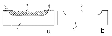
図3aにシリコンウェハ4が示され、シリコンウェハ上に多孔質化した領域をマスキングするために、酸化珪素および窒化珪素からなるマスク5,6を形成する。多孔質シリコン7を除去する前に、まず酸化珪素、窒化珪素または炭化珪素またはこれらの組合せ物からなるマスクを除去することができ、これにより図3bによりくぼみ8が残り、くぼみは周辺領域に図2の実施例のような突出するマスク部分を有しない。
【0030】
図5aはメンブランセンサーアレー20の1つの例の平面図を示す。バルクシリコン21上に自立するメンブラン領域22が形成され(図5b参照)、メンブラン領域は、放熱体として作用する、n−ドーピングシリコンからなる枠領域25とともに格子23により互いに断熱されている。格子23および枠領域25の一部は自立性であり、これは断熱を更に改良する。
【0031】
図5aおよび5bの配置は、例えば中間工程として多孔質シリコンを製造する、表面マイクロメカニック法により実現する。マスキングとして枠領域25を有する格子状のn−ドーピング領域23を使用する。例えばp−ドーピングバルクシリコン21中のn−ドーピング格子23および枠25のドーピングはイオン注入によりまたは拡散工程により行う。イオン注入の場合は注入エネルギーにより注入領域の深さを調節することができる。放熱体の厚さおよびそれとともにこれから生じる、特に周辺領域に対する熱伝導性は、これにより広い範囲で測定することができる。拡散工程の場合はドーピング物質の量、拡散時間および拡散温度によりドーピング深さを調節できる。
【0032】
一般に拡散により10μmより大きいドーピング深さが達成されるが、イオン注入の場合は5μmまでの範囲の深さである。中間工程として多孔質シリコンの製造を用意する工程は、以下のように概略的に分類できる。
【0033】
a)多孔質シリコンの製造
b)多孔質化したシリコンの場合による部分的酸化
c)メンブラン24の析出(図5b参照)
d)センサー層の析出および構造化(図5aおよび5bに示されていない)
e)メンブランの不活性化
f)メンブラン中の開口の製造(図示されていない)
g)多孔質シリコンもしくは酸化した多孔質シリコンの除去。
【0034】
n−ドーピングマスキングを使用する代わりに、十分な厚さを有する、例えば酸化珪素/窒化珪素層30(図6参照)のようなマスキング層を使用することができる。多孔質シリコンを製造する場合は、マスキングをn−ドーピングマスキングと同じ方法で等方性エッチング工程にもとづき横方向にアンダーエッチングする。図6aにはシリコンウェハ32に形成されている多孔質化した領域31がマスキング30の下側に明らかなアンダーエッチングで示されている。多孔質シリコンを局所的に製造した後にマスキング30を除去し、多孔質シリコンを場合により酸化した後にセンサーメンブラン33(図6b参照)を析出する。センサー素子(図示されていない)を製造した後に、場合により酸化した多孔質シリコンを、メンブラン33中の相当する開口により表面から除去する。より簡単な使用のために、多孔質または場合により酸化した多孔質シリコン31を放置することもでき、これによりくぼみ34(図6b参照)が生じない。約100分の1に減少した熱伝導性により、多孔質または場合により酸化した多孔質シリコンを放置する場合にも断熱が保証される。しかしながら空気、真空または充填ガスが衝突するくぼみ34の熱伝導性に関するQ値は達成されない。
【0035】
本発明の方法により、個々のメンブラン領域35の間隔を約20〜50μmの最小値に減少することができる、メンブランセンサーを実現することができる。
【0036】
メンブランセンサーアレーの構成は格子構造に限定されない。放熱体の他の自由な選択可能な形が考えられる。図7は、例えばシリコンバルク材料42内部の自立するメンブラン領域41を分離するための線形の放熱体としてのウェブ40を有する実施態様を示す。
【0037】
図4による実施態様においては、シリコンウェハ11の裏面の異方性プラズマエッチング工程により放熱体としてウェブ10を形成する。ウェブ10は自立性である。メンブラン12上に、ウェブ10の間にセンサー素子を配置することができ、センサー素子は放熱体として作用するウェブ10により互いに断熱されている。
【図面の簡単な説明】
【図1】多孔質シリコンを製造するためのマスキングとしてドーピング領域を有するシリコンウェハの断面図である。
【図2】図1による多孔質シリコンをエッチングにより除去した断面図である。
【図3】図1および図2に匹敵する配置であるが、多孔質シリコンを製造するために後で析出したマスキング層を使用したシリコンウェハの断面図である。
【図4】ウェハ裏面をエッチングした後のシリコンウェハの断面図である。
【図5】メンブランセンサーアレーの平面図および断面図である。
【図6】異なる製造段階の他のメンブランセンサーアレーの断面図である。
【図7】他のメンブランセンサーアレーの平面図である。[0001]
BACKGROUND OF THE INVENTION
The present invention relates to a method for manufacturing a membrane sensor array according to the superordinate concept of
[0002]
[Prior art]
A method of manufacturing a membrane sensor having a semiconductor material support and having at least one flat membrane region as a support for a sensor layer on the support is already known. If the membrane sensor array has a plurality of flat membrane regions, the membrane regions are more regular with a web of material having a clearly improved thermal conductivity compared to the membrane and the lateral perimeter of the web. Are insulated from each other.
[0003]
Membrane sensors currently on the market are often realized as thin films. For this purpose, a layer system having a thickness of several tens of nm to several μm is deposited on the support substrate, and then the support substrate is removed in a predetermined region in order to obtain a self-supporting membrane region. The sensor element is then placed in the center of the membrane, for example by a self-supporting arrangement of the membrane, which is insulated from the surrounding support substrate, which is preferred for temperature and flow sensors.
[0004]
There are two ways to expose the membrane.
[0005]
1. Surface micromechanics (OMM) using a sacrificial layer that is generally coated on the surface of a support substrate before depositing the membrane. The sacrificial layer is later removed from the surface of the sensor by a melt opening in the membrane, resulting in a self-supporting structure. This surface micromechanical process is relatively expensive due to the need for a separate sacrificial layer.
[0006]
2. Bulk micromechanics by exposing the membrane from the backside of the support substrate by an etching process, i.e. by etching the opening through a full thickness wafer, for example.
[0007]
A sensor array is required for many uses. For this purpose, a plurality of the same sensors are arranged linearly in parallel or two-dimensionally. If a temperature sensor is used, it must be separated from one another by a heat sink to allow spatial resolution of the measurement signal.
[0008]
There are various possibilities for producing a heat sink. A layer of good heat conductive material is deposited on the surface of the membrane and structured, and the remaining structure of good heat conductive material is used as a heat sink.
[0009]
However, the membrane can also be exposed using a bulk micromechanic process so that a web of bulk material remains between the individual membrane regions. In the case of a bulk micromechanical membrane sensor, the back membrane is generally exposed by anisotropic etching, for example, using KOH (potassium hydroxide). In this case, etching requires significantly more space on the backside of the substrate than is necessary for the original membrane structure, despite its anisotropy. This limits the integration density in this method.
[0010]
[Problems to be solved by the invention]
The object of the present invention is to reduce the manufacturing cost of the membrane sensor array, in particular to provide a membrane sensor array with an improved integration density, which likewise enables a reduction of the manufacturing cost.
[0011]
[Means for Solving the Problems]
The object is solved by the method according to claim 1 or 5 and the membrane sensor according to claim 6.
[0012]
According to the present invention, a plurality of flat membrane regions are first arranged on a semiconductor material support as a support layer of a sensor element, and the flat membrane regions are clearly compared with the membrane region and the lateral peripheral portion of the web. We start with a method of manufacturing a membrane sensor array with a semiconductor material support that is insulated from one another by a web of material with improved thermal conductivity. The term membrane region is understood within the scope of the present invention not only to be a self-supporting layer, but in the simplest case to be a single layer placed in a volume that is less thermally conductive than the web. The core of the present invention is to maintain the masking for the next step of forming the porous semiconductor material at the position where the web is formed for heat insulation on the semiconductor material support, and to protect the semiconductor material not protected by the masking. A membrane region is produced by making the substrate porous and coating a continuous membrane layer on the semiconductor material support or the porous region, for example. In this way, it is possible to achieve a high integration density of the membrane sensor array in which the individual sensors are insulated to a sufficient extent. In this case, the knowledge that a porous semiconductor material can be produced with a relatively fine structure by appropriate masking is utilized. This makes it possible to produce correspondingly fine webs that can be arranged closely in parallel accordingly, which in general allows for a high density of array sensors. Insulation occurs when the remaining semiconductor web is removed by the porous and semiconductive material as compared to the porous semiconducting material or, as will be described in detail below, possibly by gas filling. It is obtained by having a clearly higher thermal conductivity than a hollow having.
[0013]
In a particularly advantageous embodiment of the invention, it is advantageous to use a stable layer, for example silicon oxide, silicon nitride or silicon carbide or a combination thereof, for masking, in producing a porous semiconductor material. It is. This is a relatively simple possibility of masking, in which a web-shaped radiator can be realized without protruding areas after further removal of the masking layer, based on an under-etching process. However, this method cannot form a self-supporting web. That is, the web always remains bonded to the bulk material of the semiconductor material support.
[0014]
In order to manufacture a heat sink in the form of a free-standing web having a defined width and height, the semiconductor material support has a predetermined depth as a mask at the position where the web is formed for thermal insulation. It is proposed to maintain a suitable doping part and to make the semiconductor material not assigned by the doping part porous in the peripheral part of the web.
[0015]
The porous semiconductor region is preferably removed by etching after covering the membrane region. In this way, a particularly self-supporting web structure is formed when the semiconductor region surrounding the web in a continuous bath is made porous. A self-supporting web is sufficient to provide a heat sink that is sufficient for favorable thermal insulation. In this case, this method has the advantage that no additional sacrificial layer or other metal layer, for example forming a heat sink, is required. Rather, the base of the membrane sensor array below the membrane region can be formed entirely from the semiconductor material of the support, for example in the form of a continuous membrane layer.
[0016]
In the case of a method known per se for producing porous silicon, an electrochemical reaction between hydrofluoric acid and silicon is generally used, and in this case, a sponge-like structure is formed in the silicon. For this purpose, the silicon semiconductor support (generally a silicon wafer) must be connected to the anode with respect to the hydrofluoric acid electrolyte. Porous silicon is produced by partial etching to said depth, for example by electrochemical etching (anodization) of silicon in a mixture of hydrofluoric acid / ethanol. In order to etch silicon, defective electrons (holes) are required at the interface between the silicon and the electrolyte, which is supplied by a flowing current. If the current density is less than the critical current density j KRIT, the holes are diffused by the electric field applied in the depressions present on the surface, where advantageous etching takes place. In the case of p-doped silicon, for example, holes can no longer penetrate into this region due to quantum effects, and the region between the recesses is etched laterally to a minimum thickness until the etching process stops. In this way, a sponge-like skeleton structure consisting of silicon and free-etched holes is produced. Since the etching process is performed only on the hole tip region when forming the skeleton structure, the already etched silicon sponge structure is maintained. As a result, the hole diameter in the already etched region remains substantially unchanged. The pore size depends on the concentration of HF in hydrofluoric acid, doping and current density, and may be several nanometers to several tens of nanometers. Similarly, the porosity can be adjusted to a range of about 10% to 90% or more.
[0017]
Various doping substrates can be used to produce porous silicon. In general, p-doped wafers of various doping degrees are used. The size of the structure can be determined inside the porous silicon by doping.
[0018]
By forming a porous structure, silicon acquires other internal chemical and physical properties (eg, other etch rates, thermal conductivity, heat capacity, etc.) such as large internal surfaces and the bulk silicon that it surrounds. Accordingly, the reactivity is clearly improved, which allows selective etching of porous silicon relative to bulk silicon.
[0019]
In this case, the production of the web in silicon is carried out as follows.
[0020]
In the case of silicon, the knowledge that p-doped silicon and n-doped silicon in particular have significantly different etching properties can be used. Under conditions where porous silicon can be produced in p-doped silicon, this is not possible or only possible to a very small extent in n-doped silicon. Thus, as a masking layer, for example, a thin layer on the surface of a p-doped substrate can be n-doped again (by ion implantation or diffusion). In the case of electrochemical etching, porous silicon is produced only in the p-doping region. The thickness of the masking layer can vary depending on processing parameters (doping amount, implantation energy, implantation after doping material). Since the formation of porous silicon is an isotropic process, the mask is under-etched accordingly. If the web region characterized by doping is completely under-etched, a free-standing web structure results after removal of the porous silicon.
[0021]
Due to the etching of the porous semiconductor material, in the case of silicon, there are essentially two possibilities, in particular after depositing the sensor layer. One uses strongly diluted potassium hydroxide solution (KOH) and one uses hydrofluoric acid (HF). In this case, the porous silicon is still treated in an oxidation step before coating the membrane region.
[0022]
In another advantageous embodiment of the invention, a plurality of flat membrane regions are arranged on the semiconductor material support as a support layer of the sensor element, wherein the plurality of flat membrane regions are transverse to the membrane region and the web. In a method of manufacturing a membrane sensor array with a semiconductor material support, which is thermally insulated by a web of material having a clearly improved thermal conductivity compared to the surrounding part of the Forms a web from the back side of the semiconductor material support by a subsequent anisotropic plasma etching process that allows the membrane layer to be coated directly on the semiconductor material support to achieve at least a nearly vertical etched side in the semiconductor. It is advantageous to do so. By this method, an improvement in integration density can be achieved to a considerable extent, especially with respect to membrane sensor arrays, despite the use of bulk micromechanical methods.
[0023]
Furthermore, the present invention has a support made of a semiconductor material, and a flat membrane region that exists in parallel on the support is arranged as a support layer of the sensor element, and this membrane region is located next to the membrane region and the web. Starting from a membrane sensor array in which the webs are insulated from one another by a web of material having a significantly improved thermal conductivity compared to the peripheral part of the direction, the web being formed from a semiconducting material of the support. The central idea of this configuration of the invention is that the width of the web in direct contact with the membrane region is less than 50 μm. The recognition that forms the basis of this idea is that, for example, when the web is placed under a continuous membrane and the membrane is divided into membrane regions, this type of formed web has a sufficient function as a heat sink. To meet.
[0024]
In order to obtain a simple structure of the membrane sensor array, it is further proposed that the web is formed only from the semiconductor material of the support.
[0025]
For example, in the case of silicon wafers, if masking is used by doping a p-doped wafer to produce a web, the web width and web thickness can be easily adjusted by the doping process, thereby The heat conduction value can be controlled in a sensitive manner. Exactly this masking process makes it possible to produce thin webs when viewed in the vertical direction, which meets the requirements of the heat sink. It has been found that a web thickness of less than 30 μm is already sufficient.
[0026]
The structure of the heat dissipation body advantageously consists of a web, for example a web arranged in a cruciform shape and a frame area joined to the web. In order to produce this heat sink structure for the surrounding semiconductor material in the process of forming the porous semiconductor material, it is advantageous if the web and the frame region are correspondingly doped.
[0027]
【Example】
The invention will be explained in greater detail by means of an embodiment shown in the drawing.
[0028]
FIG. 1 shows a p-doped
[0029]
A
[0030]
FIG. 5 a shows a plan view of one example of
[0031]
The arrangement of FIGS. 5a and 5b is realized, for example, by a surface micromechanical method in which porous silicon is produced as an intermediate step. A lattice-shaped n-
[0032]
In general, a doping depth greater than 10 μm is achieved by diffusion, but in the case of ion implantation, the depth is in the range of up to 5 μm. The process of preparing the production of porous silicon as an intermediate process can be roughly classified as follows.
[0033]
a) Production of porous silicon b) Partial oxidation in the case of porous silicon c) Deposition of membrane 24 (see FIG. 5b)
d) Deposition and structuring of the sensor layer (not shown in FIGS. 5a and 5b)
e) Deactivation of the membrane f) Production of openings in the membrane (not shown)
g) Removal of porous silicon or oxidized porous silicon.
[0034]
Instead of using n-doping masking, a masking layer having a sufficient thickness, such as the silicon oxide / silicon nitride layer 30 (see FIG. 6), can be used. When manufacturing porous silicon, masking is under-etched in the lateral direction based on an isotropic etching process in the same manner as n-doping masking. In FIG. 6a, the
[0035]
By the method of the present invention, a membrane sensor can be realized in which the distance between the
[0036]
The configuration of the membrane sensor array is not limited to the lattice structure. Other freely selectable shapes of the radiator are conceivable. FIG. 7 shows an embodiment having a
[0037]
In the embodiment according to FIG. 4, the
[Brief description of the drawings]
FIG. 1 is a cross-sectional view of a silicon wafer having a doping region as a mask for producing porous silicon.
FIG. 2 is a cross-sectional view of the porous silicon according to FIG. 1 removed by etching.
FIG. 3 is a cross-sectional view of a silicon wafer in an arrangement comparable to FIGS. 1 and 2, but using a masking layer deposited later to produce porous silicon.
FIG. 4 is a cross-sectional view of a silicon wafer after etching the wafer back surface.
FIG. 5 is a plan view and a cross-sectional view of a membrane sensor array.
FIG. 6 is a cross-sectional view of another membrane sensor array at a different manufacturing stage.
FIG. 7 is a plan view of another membrane sensor array.
Claims (11)
Priority Applications (1)
| Application Number | Priority Date | Filing Date | Title |
|---|---|---|---|
| JP2001355118A JP4215424B2 (en) | 2001-11-20 | 2001-11-20 | Manufacturing method of membrane sensor array and membrane sensor array |
Applications Claiming Priority (1)
| Application Number | Priority Date | Filing Date | Title |
|---|---|---|---|
| JP2001355118A JP4215424B2 (en) | 2001-11-20 | 2001-11-20 | Manufacturing method of membrane sensor array and membrane sensor array |
Publications (2)
| Publication Number | Publication Date |
|---|---|
| JP2003165097A JP2003165097A (en) | 2003-06-10 |
| JP4215424B2 true JP4215424B2 (en) | 2009-01-28 |
Family
ID=19166869
Family Applications (1)
| Application Number | Title | Priority Date | Filing Date |
|---|---|---|---|
| JP2001355118A Expired - Fee Related JP4215424B2 (en) | 2001-11-20 | 2001-11-20 | Manufacturing method of membrane sensor array and membrane sensor array |
Country Status (1)
| Country | Link |
|---|---|
| JP (1) | JP4215424B2 (en) |
Families Citing this family (2)
| Publication number | Priority date | Publication date | Assignee | Title |
|---|---|---|---|---|
| DE202008017782U1 (en) * | 2007-07-26 | 2010-06-10 | Fraunhofer-Gesellschaft zur Förderung der angewandten Forschung e.V. | Silicon solar cell with a back etched highly doped surface layer area |
| KR101781553B1 (en) * | 2011-08-22 | 2017-09-26 | 삼성전자주식회사 | Capacitive transducer and methods of manufacturing and operating the same |
-
2001
- 2001-11-20 JP JP2001355118A patent/JP4215424B2/en not_active Expired - Fee Related
Also Published As
| Publication number | Publication date |
|---|---|
| JP2003165097A (en) | 2003-06-10 |
Similar Documents
| Publication | Publication Date | Title |
|---|---|---|
| CN1564780B (en) | Method for producing semiconductor component and semiconductor component | |
| US7427526B2 (en) | Deposited thin films and their use in separation and sacrificial layer applications | |
| EP1417151B1 (en) | Method for the fabrication of suspended porous silicon microstructures and application in gas sensors | |
| JP5559369B2 (en) | Sensor and sensor manufacturing method | |
| US7276277B2 (en) | Micromechanical component, in particular a sensor element, having a stabilized membrane and a method of producing such a component | |
| CA2406214A1 (en) | Deposited thin films and their use in separation and sarcrificial layer applications | |
| JP2004502555A (en) | Method of manufacturing semiconductor component and semiconductor component manufactured by the method | |
| JP2009538238A (en) | Micromachine component and manufacturing method thereof | |
| JP2016193490A (en) | Method of manufacturing semiconductor device, and semiconductor devices | |
| JP5097256B2 (en) | Method of forming curved surface | |
| JPH07193052A (en) | Micro cavity forming method and micro device having micro cavity | |
| US20050016288A1 (en) | Micromechanical apparatus, pressure sensor, and method | |
| JP4327456B2 (en) | Micromechanics component and manufacturing method thereof | |
| US6506621B1 (en) | Method for producing a diaphragm sensor array and diaphragm sensor array | |
| US6759265B2 (en) | Method for producing diaphragm sensor unit and diaphragm sensor unit | |
| JP4215424B2 (en) | Manufacturing method of membrane sensor array and membrane sensor array | |
| US6521313B1 (en) | Method for producing a diaphragm sensor unit and diaphragm sensor unit | |
| US7803646B2 (en) | Method for producing a component having a semiconductor substrate and component | |
| US20090061601A1 (en) | Method and apparatus for improved pumping medium for electro-osmotic pumps | |
| JP4243447B2 (en) | Membrane sensor unit manufacturing method, membrane sensor unit and membrane sensor array | |
| KR100802967B1 (en) | Membrane sensor array and its manufacturing method | |
| KR100881581B1 (en) | Membrane sensor unit and its manufacturing method | |
| JP4007395B2 (en) | Method of forming curved surface | |
| JP4007394B2 (en) | Method of forming curved surface | |
| JP4743102B2 (en) | Method of forming curved surface |
Legal Events
| Date | Code | Title | Description |
|---|---|---|---|
| A621 | Written request for application examination |
Free format text: JAPANESE INTERMEDIATE CODE: A621 Effective date: 20041119 |
|
| A131 | Notification of reasons for refusal |
Free format text: JAPANESE INTERMEDIATE CODE: A131 Effective date: 20070822 |
|
| A601 | Written request for extension of time |
Free format text: JAPANESE INTERMEDIATE CODE: A601 Effective date: 20071121 |
|
| A602 | Written permission of extension of time |
Free format text: JAPANESE INTERMEDIATE CODE: A602 Effective date: 20071127 |
|
| A601 | Written request for extension of time |
Free format text: JAPANESE INTERMEDIATE CODE: A601 Effective date: 20071225 |
|
| A602 | Written permission of extension of time |
Free format text: JAPANESE INTERMEDIATE CODE: A602 Effective date: 20071228 |
|
| A521 | Written amendment |
Free format text: JAPANESE INTERMEDIATE CODE: A523 Effective date: 20080122 |
|
| A131 | Notification of reasons for refusal |
Free format text: JAPANESE INTERMEDIATE CODE: A131 Effective date: 20080514 |
|
| TRDD | Decision of grant or rejection written | ||
| A01 | Written decision to grant a patent or to grant a registration (utility model) |
Free format text: JAPANESE INTERMEDIATE CODE: A01 Effective date: 20081003 |
|
| A01 | Written decision to grant a patent or to grant a registration (utility model) |
Free format text: JAPANESE INTERMEDIATE CODE: A01 |
|
| A61 | First payment of annual fees (during grant procedure) |
Free format text: JAPANESE INTERMEDIATE CODE: A61 Effective date: 20081104 |
|
| R150 | Certificate of patent or registration of utility model |
Free format text: JAPANESE INTERMEDIATE CODE: R150 |
|
| FPAY | Renewal fee payment (event date is renewal date of database) |
Free format text: PAYMENT UNTIL: 20111114 Year of fee payment: 3 |
|
| FPAY | Renewal fee payment (event date is renewal date of database) |
Free format text: PAYMENT UNTIL: 20121114 Year of fee payment: 4 |
|
| FPAY | Renewal fee payment (event date is renewal date of database) |
Free format text: PAYMENT UNTIL: 20131114 Year of fee payment: 5 |
|
| LAPS | Cancellation because of no payment of annual fees |