JP4189403B2 - Rectifier circuit and RFID tag using the same - Google Patents
Rectifier circuit and RFID tag using the same Download PDFInfo
- Publication number
- JP4189403B2 JP4189403B2 JP2005308786A JP2005308786A JP4189403B2 JP 4189403 B2 JP4189403 B2 JP 4189403B2 JP 2005308786 A JP2005308786 A JP 2005308786A JP 2005308786 A JP2005308786 A JP 2005308786A JP 4189403 B2 JP4189403 B2 JP 4189403B2
- Authority
- JP
- Japan
- Prior art keywords
- capacitor
- rectifier circuit
- voltage
- circuit
- terminal
- Prior art date
- Legal status (The legal status is an assumption and is not a legal conclusion. Google has not performed a legal analysis and makes no representation as to the accuracy of the status listed.)
- Expired - Fee Related
Links
Images


Landscapes
- Rectifiers (AREA)
Description
本発明は、ゲート端子とソース端子との間にキャパシタが接続されたMOSトランジスタを整流素子として備えた高利得整流回路と、その高利得整流回路を用いたRFID(Radio Frequency Identification)タグに関する。 The present invention relates to a high gain rectifier circuit including, as a rectifier, a MOS transistor having a capacitor connected between a gate terminal and a source terminal, and an RFID (Radio Frequency Identification) tag using the high gain rectifier circuit.
整流回路は、ダイオードの整流特性を利用することにより、交流信号を直流信号に変換する。整流回路を半導体集積回路によって実現する場合、通常、ソース端子とゲート端子とを互いに接続した、いわゆるダイオード接続のMOSトランジスタを整流ダイオードとして用いる。例えば、トリプルウェルによって基板とアイソレーションが取られているNMOSトランジスタを用いた整流ダイオードでは、ドレイン端子およびソース端子はそれぞれN領域に接続され、ソース端子は、トランジスタ下部のPウェルに接続されたバックゲート端子にも接続される。これにより、ソース端子とドレイン端子との間にPN接続が形成されたダイオード素子が実現される。 The rectifier circuit converts an AC signal into a DC signal by using the rectification characteristics of the diode. When the rectifier circuit is realized by a semiconductor integrated circuit, a so-called diode-connected MOS transistor in which a source terminal and a gate terminal are connected to each other is usually used as a rectifier diode. For example, in a rectifier diode using an NMOS transistor that is isolated from the substrate by a triple well, the drain terminal and the source terminal are each connected to the N region, and the source terminal is connected to the P well below the transistor. Also connected to the gate terminal. Thereby, a diode element in which a PN connection is formed between the source terminal and the drain terminal is realized.
近年、その応用分野の広さから、RFIDタグが注目されている。このRFIDタグにおいては整流回路が必須である。RFIDタグは、アンテナに誘起された交流電流から、RFIDタグ内の集積回路を駆動する直流電源の生成と、データ信号の復調とを行う。これら処理の際に整流回路が必要となる。 In recent years, RFID tags have attracted attention because of their wide application fields. In this RFID tag, a rectifier circuit is essential. The RFID tag generates a DC power source for driving an integrated circuit in the RFID tag and demodulates a data signal from an AC current induced in the antenna. A rectifier circuit is required for these processes.
RFIDタグに用いられる整流回路として、例えば、特許文献1や非特許文献1に開示の構成が知られているが、これら構成も、上記したダイオード接続のMOSトランジスタを利用することに変わりはない。ただし、MOSトランジスタの閾値がPN接合の閾値より小さい場合、整流特性は、MOSトランジスタの特性により決まり、そのMOSトランジスタの閾値をPN接合の閾値として有するダイオードの整流特性と等価な特性を示す。
For example, configurations disclosed in
ダイオードにおいて整流特性を発現させるためには、ダイオード接続されたMOSトランジスタのPN接続端子間に、PN接合の閾値以上の電圧又はMOSトランジスタの閾値以上の電圧を印加する必要がある。この電圧印加は、例えば、MOSトランジスタのゲートとソースとの間にキャパシタを接続し、このキャパシタに0以上且つ上記閾値以下の電圧(以下、バイアス電圧と称する)を保持させることにより実現できる。これによって、上記バイアス電圧未満の実効値を有する交流信号が整流回路に入力された場合であってもその信号の整流を行なうことができる。これは、RFIDタグにとっては、リーダ/ライタから送信された微弱な信号を受信することができ、リーダ/ライタとの間の通信可能な距離を拡大できることを意味する。通信距離の拡大は、一つのリーダ/ライタによる複数のRFIDタグの同時認識を容易にし、RFIDタグの応用範囲を広げることになる。 In order to develop rectification characteristics in the diode, it is necessary to apply a voltage higher than the threshold of the PN junction or a voltage higher than the threshold of the MOS transistor between the PN connection terminals of the diode-connected MOS transistor. This voltage application can be realized, for example, by connecting a capacitor between the gate and the source of a MOS transistor and holding the voltage not less than 0 and not more than the threshold value (hereinafter referred to as a bias voltage). Thus, even when an AC signal having an effective value less than the bias voltage is input to the rectifier circuit, the signal can be rectified. This means that the RFID tag can receive a weak signal transmitted from the reader / writer and can increase the communicable distance between the reader / writer. The expansion of the communication distance facilitates simultaneous recognition of a plurality of RFID tags by one reader / writer, and widens the application range of the RFID tags.
しかしながら、上記キャパシタに蓄えられた電荷は、該キャパシタが接続されたMOSトランジスタのリーク電流によって放電されるため、キャパシタ間の電圧は時間の経過とともに減少する。これは、整流可能な交流信号の大きさが増加することを意味する。換言すれば、整流回路の変換利得が減少する。そこで、整流回路に対し、上記キャパシタを充電するための制御信号を定期的に送信する必要がある。ところが、カウンタ等によって定期的にその制御信号を生成するのであっては、必要以上にキャパシタへの充電動作を繰り返すことになる。特に、RFIDタグのように、電力消費の低下が重要な設計因子となるデバイスにおいては、そのような無駄な電力消費は避けたい。 However, since the electric charge stored in the capacitor is discharged by the leakage current of the MOS transistor to which the capacitor is connected, the voltage between the capacitors decreases with time. This means that the size of the AC signal that can be rectified increases. In other words, the conversion gain of the rectifier circuit is reduced. Therefore, it is necessary to periodically transmit a control signal for charging the capacitor to the rectifier circuit. However, if the control signal is periodically generated by a counter or the like, the capacitor charging operation is repeated more than necessary. In particular, in a device such as an RFID tag in which a reduction in power consumption is an important design factor, it is desirable to avoid such wasteful power consumption.
また、上記したバイアス電圧は、バイアス対象となるMOSトランジスタの閾値電圧程度がよいとされる。これは、閾値電圧以上ではMOSトランジスタに流れる電流が逆流し、これにより整流回路の利得が低下するためである。ところが、MOSトランジスタの閾値電圧は、該MOSトランジスタの製造ばらつきによって変動するため、バイアス電圧を単に所定値に固定したのであっては、製造ばらつきにより整流回路の利得が小さくなる。 Further, the above bias voltage is preferably about the threshold voltage of the MOS transistor to be biased. This is because the current flowing through the MOS transistor flows backward above the threshold voltage, thereby reducing the gain of the rectifier circuit. However, since the threshold voltage of the MOS transistor varies depending on the manufacturing variation of the MOS transistor, if the bias voltage is simply fixed to a predetermined value, the gain of the rectifier circuit becomes small due to the manufacturing variation.
本発明は、上記に鑑みてなされたものであって、整流回路の駆動に伴う消費電力と素子ばらつきの影響を低減することができる高利得整流回路とそれを用いたRFIDタグを提供することを目的とする。 The present invention has been made in view of the above, and provides a high-gain rectifier circuit capable of reducing the influence of power consumption and element variations accompanying driving of the rectifier circuit, and an RFID tag using the same. Objective.
上述した課題を解決し、目的を達成するために、本発明にかかる整流回路は、ゲート端子とソース端子との間に第1のキャパシタが接続されるとともに前記ソース端子とドレイン端子との間においてダイオード特性を示す第1のMOSトランジスタと、制御信号に基づいて所定のバイアス電圧を前記第1のキャパシタに供給するスイッチング部と、を有する整流部と、前記第1のMOSトランジスタを模擬した第2のMOSトランジスタと、前記第1のキャパシタを模擬した第2のキャパシタと、前記制御信号に基づいて前記バイアス電圧を前記第2のキャパシタに供給するダミースイッチング部と、を有し、前記第2のキャパシタの電位に基づいて前記制御信号を生成するバイアス設定部と、を備え、前記第1のMOSトランジスタは、前記ソース端子と前記ドレイン端子の一方から交流信号を入力し、前記ダイオード特性による整流作用によって前記交流信号を直流信号に変換して該直流信号を前記ソース端子と前記ドレイン端子の他方から出力する。 To solve the above problems and achieve the object, rectifier circuit that written to the present invention includes a first capacitor is connected Rutotomoni the source and drain terminals between the gate terminal and the source terminal simulating a first MOS transistor indicating the diode characteristic, a rectifier unit having a switching unit for supplying to said first capacitor a predetermined bias voltage based on the control signal, the first MOS transistor between the a second MOS transistor having a second capacitor simulating the first capacitor, and a dummy switching unit for supplying the bias voltage to the second capacitor based on the control signal, the and a bias setting unit for generating the control signal based on the potential of the second capacitor, said first MOS transistor, before Enter an AC signal from one of the drain terminal and the source terminal, and outputs a direct current signal by converting the AC signal into a DC signal by the rectifier action of the diode characteristics from the other of the drain terminal and the source terminal.
また、本発明にかかるRFIDタグは、上記した高利得整流回路を備える。 The RFID tag according to the present invention includes the above-described high gain rectifier circuit.
本発明にかかる高利得整流回路およびRFIDタグは、整流部を構成するMOSトランジスタをバイアスするための無駄な充電動作が低減され、消費電力の低下を実現することができる。また、高利得整流回路間の製造ばらつきに影響されず、常に一定値以上の利得を有する整流を実現することができる。 In the high gain rectifier circuit and the RFID tag according to the present invention, useless charging operation for biasing the MOS transistor constituting the rectifier unit is reduced, and a reduction in power consumption can be realized. Further, rectification always having a gain of a certain value or more can be realized without being affected by manufacturing variations between high gain rectifier circuits.
以下に、本発明にかかる高利得整流回路およびそれを用いたRFIDタグの実施の形態を図面に基づいて詳細に説明する。 Embodiments of a high gain rectifier circuit and an RFID tag using the same according to the present invention will be described below in detail with reference to the drawings.
(実施の形態1)
本発明の実施の形態1にかかる高利得整流回路は、整流素子として機能するMOSトランジスタ(以下、整流MOSトランジスタと称する)を模擬したMOSトランジスタ(以下、模擬MOSトランジスタと称する)を備え、その模擬MOSトランジスタのゲート端子とソース端子との間に接続されたキャパシタの電位を監視することによって、整流MOSトランジスタに接続されたキャパシタを最適なタイミングで充電することを特徴としている。
(Embodiment 1)
A high gain rectifier circuit according to a first embodiment of the present invention includes a MOS transistor (hereinafter referred to as a simulated MOS transistor) that simulates a MOS transistor (hereinafter referred to as a rectified MOS transistor) that functions as a rectifier element, and simulates the same. The capacitor connected to the rectifying MOS transistor is charged at an optimal timing by monitoring the potential of the capacitor connected between the gate terminal and the source terminal of the MOS transistor.
図1は、実施の形態1にかかる高利得整流回路を示す回路図である。図1に示すように、実施の形態1にかかる高利得整流回路は、整流回路200とバイアス設定回路100とを備えている。
FIG. 1 is a circuit diagram illustrating a high gain rectifier circuit according to a first embodiment. As shown in FIG. 1, the high gain rectifier circuit according to the first embodiment includes a
整流回路200は、入力された交流信号を整流する整流部と、その整流部を構成するキャパシタに所定の電位を与えるスイッチング部とから構成される。
The
整流部は、直列に接続されたNMOSトランジスタM1およびM2を備えている。NMOSトランジスタM1は、バックゲート端子とソース端子とが接続され、ドレイン端子がプラス端子T1に接続されている。また、ゲート端子とソース端子との間に、キャパシタC12が接続されている。この接続構成により、NMOSトランジスタM1は、キャパシタC12の両端の電圧によってバイアスされるので高利得な整流素子として機能する。 The rectifying unit includes NMOS transistors M1 and M2 connected in series. In the NMOS transistor M1, the back gate terminal and the source terminal are connected, and the drain terminal is connected to the plus terminal T1. A capacitor C12 is connected between the gate terminal and the source terminal. With this connection configuration, the NMOS transistor M1 functions as a high-gain rectifying element because it is biased by the voltage across the capacitor C12.
同様に、NMOSトランジスタM2は、バックゲート端子とソース端子とが接続され、ソース端子がマイナス端子T2に接続されている。また、ゲート端子とソース端子との間に、キャパシタC22が接続されている。このNMOSトランジスタM2もまた、NMOSトランジスタM1と同様に高利得な整流素子として機能し、キャパシタC22の両端の電圧によってバイアスされる。 Similarly, in the NMOS transistor M2, the back gate terminal and the source terminal are connected, and the source terminal is connected to the minus terminal T2. A capacitor C22 is connected between the gate terminal and the source terminal. The NMOS transistor M2 also functions as a high-gain rectifying element, like the NMOS transistor M1, and is biased by the voltage across the capacitor C22.
NMOSトランジスタM1のソース端子とNMOSトランジスタM2のドレイン端子とは互いに接続されており、その接続点に、キャパシタC1の一端が接続されている。キャパシタC1の他端は、交流信号が入力される信号入力端子TAに接続されている。このキャパシタC1は、結合容量として機能する。特に、キャパシタC1は、本実施の形態にかかる高利得整流回路をRFIDタグにおいて使用する場合、アンテナ(例えば、ループアンテナ)に接続され、直列共振キャパシタとしても機能する。 The source terminal of the NMOS transistor M1 and the drain terminal of the NMOS transistor M2 are connected to each other, and one end of the capacitor C1 is connected to the connection point. The other end of the capacitor C1 is connected to a signal input terminal TA to which an AC signal is input. This capacitor C1 functions as a coupling capacitance. In particular, when the high gain rectifier circuit according to this embodiment is used in an RFID tag, the capacitor C1 is connected to an antenna (for example, a loop antenna) and functions as a series resonant capacitor.
NMOSトランジスタM1のドレイン端子とNMOSトランジスタM2のソース端子との間には、キャパシタC2が接続されている。NMOSトランジスタM1およびM2によって半波整流された信号は、このキャパシタC2によって平滑される。この平滑により、キャパシタC2の両端、すなわちプラス端子T1とマイナス端子T2との間から直流電圧を取り出すことができる。 A capacitor C2 is connected between the drain terminal of the NMOS transistor M1 and the source terminal of the NMOS transistor M2. The signal half-wave rectified by the NMOS transistors M1 and M2 is smoothed by the capacitor C2. By this smoothing, a DC voltage can be taken out from both ends of the capacitor C2, that is, between the plus terminal T1 and the minus terminal T2.
NMOSトランジスタM1およびM2は、トリプルウェル構造で形成され、基板とアイソレーションされている。各ソース端子は、NMOSトランジスタ下部のP型ウェルに接続され、各ドレイン端子はN領域に接続されており、MOSトランジスタによるPN接続を模擬した整流素子部として動作する。 The NMOS transistors M1 and M2 are formed in a triple well structure and are isolated from the substrate. Each source terminal is connected to a P-type well below the NMOS transistor, and each drain terminal is connected to the N region, and operates as a rectifying element unit that simulates a PN connection by a MOS transistor.
一方、スイッチング部は、制御信号V1に基いて、バイアス電圧源210から供給される電圧を上記したキャパシタC12およびC22へと与える。キャパシタC12およびC22に与えられる電圧は、NMOSトランジスタM1およびM2が整流特性を示すのに必要な閾値電圧未満の電圧(以下、バイアス電圧VTと称する)であり、例えば、0V〜1.0Vの範囲である。このバイアス電圧VTは、特に、閾値電圧近傍の値(例えば、0.6V)であるのが好ましい。これにより、NMOSトランジスタM1およびM2は、信号入力端子TAに、上記した閾値電圧以下の実効値を有する交流信号が入力された場合であってもそれを整流することができる。例えば、バイアス電圧VTが0.6Vである場合、実効値が100mV程度の交流信号も整流することができる。
On the other hand, the switching unit, a control signal based on V 1, gives a voltage supplied from the
スイッチング部は、具体的には、図1に示すように、トランスファゲートとして機能する複数のNMOSトランジスタM11〜M14,M21〜M24と、インバータINV1およびINV2と、バイアス電圧源210とを備えて構成される。NMOSトランジスタM11およびM12は直列に接続され、バイアス電圧源210の正極端子に接続された第1のプラスライン上に配置されている。この第1のプラスラインは、バイアス電圧源210の正極端子から、NMOSトランジスタM12、M11を介して、キャパシタC12の一端であって且つNMOSトランジスタM1のゲート端子に接続される。NMOSトランジスタM13およびM14もまた直列に接続され、バイアス電圧源210の負極端子に接続された第1のマイナスライン上に配置されている。この第1のマイナスラインは、バイアス電圧源210の負極端子から、NMOSトランジスタM14、M13を介して、キャパシタC12の他端であって且つNMOSトランジスタM1のソース端子に接続される。NMOSトランジスタM11のソース端子とNMOSトランジスタM12のドレイン端子との接続点と、NMOSトランジスタM13のソース端子とNMOSトランジスタM14のドレイン端子との接続点との間には、キャパシタC11が接続されている。換言すれば、キャパシタC11は、第1のプラスラインと第1のマイナスラインの間に接続されている。
Specifically, as shown in FIG. 1, the switching unit includes a plurality of NMOS transistors M11 to M14, M21 to M24 functioning as transfer gates, inverters INV1 and INV2, and a
NMOSトランジスタM21およびM22は直列に接続され、バイアス電圧源210の正極に接続された第2のプラスライン上に配置されている。この第2のプラスラインは、バイアス電圧源210の正極端子から、NMOSトランジスタM22、M21を介して、キャパシタC22の一端であって且つNMOSトランジスタM2のゲート端子に接続される。NMOSトランジスタM23およびM24もまた直列に接続され、バイアス電圧源210の負極に接続された第2のマイナスライン上に配置されている。この第2のマイナスラインは、NMOSトランジスタM24、M23を介して、キャパシタC22の他端であって且つNMOSトランジスタM2のソース端子に接続される。NMOSトランジスタM21のソース端子とNMOSトランジスタM22のドレイン端子との接続点と、NMOSトランジスタM23のソース端子とNMOSトランジスタM24のドレイン端子との接続点との間には、キャパシタC21が接続されている。換言すれば、キャパシタC21は、第2のプラスラインと第2のマイナスラインの間に接続されている。
The NMOS transistors M21 and M22 are connected in series and are arranged on a second plus line connected to the positive electrode of the
NMOSトランジスタM11,M13,M21,M23の各ゲート端子は、インバータINV1の出力端子に接続されている。また、NMOSトランジスタM12,M14,M22,M24の各ゲート端子は、インバータINV1の入力端子に接続されている。インバータINV1の入力端子は、インバータINV2の出力端子に接続されている。 The gate terminals of the NMOS transistors M11, M13, M21, and M23 are connected to the output terminal of the inverter INV1. The gate terminals of the NMOS transistors M12, M14, M22, and M24 are connected to the input terminal of the inverter INV1. The input terminal of the inverter INV1 is connected to the output terminal of the inverter INV2.
このように構成されたスイッチング部の動作は以下のとおりである。インバータINV2に入力される制御信号V1が、論理レベル“L”を示す期間においては、NMOSトランジスタM12,M14,M22,M24はONとなり、キャパシタC11およびC21は、バイアス電圧源210によって、バイアス電圧VTと等しくなるように充電される。その間、インバータINV1の出力は、論理レベル“L”を示すため、NMOSトランジスタM11,M13,M21,M23はOFFであり、キャパシタC12およびC22は充電されない。一方、制御信号V1が論理レベル“H”を示す期間においては、NMOSトランジスタM12,M14,M22,M24はOFFとなり、NMOSトランジスタM11,M13,M21,M23はONとなるので、キャパシタC11に充電された電荷はキャパシタC12に供給され、キャパシタC21に充電された電荷はキャパシタC22に供給される。これにより、NMOSトランジスタM1のゲート−ソース間と、NMOSトランジスタM2のゲート−ソース間とにそれぞれバイアス電圧VTが印加される。
The operation of the switching unit configured as described above is as follows. During the period in which the control signal V 1 input to the
この整流回路200のインバータINV2に入力される制御信号V1は、バイアス設定回路100によって生成される。バイアス設定回路100は、ダミー整流部と、ダミースイッチング部と制御信号生成部とから構成される。ダミー整流部は、整流回路200の整流部の一部を複製した回路からなり、NMOSトランジスタM1またはM2と同じ特性のNMOSトランジスタM30と、キャパシタC12またはC22に相当するキャパシタC32とを備えている。NMOSトランジスタM30は、バックゲート端子とソース端子とが接続され、ソース端子とドレイン端子はともに接地されている。また、NMOSトランジスタM30のゲート端子とソース端子との間に、上記したキャパシタC32が接続されている。すなわち、ダミー整流部は、整流回路200の整流部を構成する整流素子のうちの一つを模擬している。
A control signal V 1 input to the
ダミースイッチング部は、整流回路200のスイッチング部を構成する回路のうち、整流部のキャパシタC12とC22のいずれか一方にバイアス電圧VTを供給するための回路に相当する構成を有する。図1においては、NMOSトランジスタM31〜M34と、キャパシタC31と、インバータINV11と、バイアス電圧源110とで構成される回路がダミースイッチング部に相当する。
The dummy switching unit has a configuration corresponding to a circuit for supplying the bias voltage V T to either one of the capacitors C12 and C22 of the rectifying unit among the circuits configuring the switching unit of the
具体的には、NMOSトランジスタM31およびM32は直列に接続され、バイアス電圧源110の正極端子に接続されたプラスライン上に配置されている。このプラスラインは、NMOSトランジスタM32、M31を介して、キャパシタC32の一端であって且つNMOSトランジスタM30のゲート端子に接続される。NMOSトランジスタM33およびM34もまた直列に接続され、バイアス電圧源110の負極端子に接続されたマイナスライン上に配置されている。このマイナスラインは、NMOSトランジスタM34、M33を介して、キャパシタC32の他端であって且つNMOSトランジスタM30のソース端子に接続される。NMOSトランジスタM31のソース端子とNMOSトランジスタM32のドレイン端子との接続点と、NMOSトランジスタM33のソース端子とNMOSトランジスタM34のドレイン端子との接続点との間には、キャパシタC31が接続されている。NMOSトランジスタM31およびM33の各ゲート端子は、インバータINV11の入力端子に接続されている。また、NMOSトランジスタM32およびM34の各ゲート端子は、インバータINV11の出力端子に接続されている。これは、整流回路200で言えば、例えば、キャパシタC12にバイアス電圧VTを供給するための回路、すなわちNMOSトランジスタM11〜M14と、キャパシタC11と、インバータINV1およびINV2と、バイアス電圧源210とからなる回路構成に相当する。特にバイアス電圧源110は、バイアス電圧源210と同じバイアス電圧VTを供給する。
Specifically, the NMOS transistors M31 and M32 are connected in series and arranged on the plus line connected to the positive terminal of the
制御信号生成部は、ダミー整流部のキャパシタC32の電位を監視し、その監視結果に基づいて制御信号V1を生成する。図1においては、インバータINV12と、参照電圧源120と、誤差増幅器130とで構成される回路が制御信号生成部に相当する。誤差増幅器130は、正相入力端子が、ダミー整流部のNMOSトランジスタM30のゲート端子に接続され、逆相入力端子が、参照電圧源120の正極端子に接続されている。誤差増幅器130の正相入力端子は、正確に言えば、キャパシタC32の一端(プラスライン側)に接続される。ここで、このキャパシタC32の一端の電位をV0と表す。また、参照電圧源120は、参照電圧VT−VXを生成する。なお、電圧VXについては後述する。以上の接続構成により、誤差増幅器130は、キャパシタC32の一端の電位V0から参照電圧VT−VXを減算した差分に相当する誤差電圧VEを出力する。
The control signal generation unit monitors the potential of the capacitor C32 of the dummy rectification unit, and generates the control signal V 1 based on the monitoring result. In FIG. 1, a circuit including an inverter INV12, a
図2は、誤差増幅器130の一例を示す回路図である。図2に示す誤差増幅器は、負荷トランジスタとして機能するPMOSトランジスタM121およびM122と、差動ペアを構成するNMOSトランジスタM123およびM124と、定電流源121とから構成され、特に、PMOSトランジスタM121およびM122は、それぞれのゲート端子とドレイン端子が正帰還となるように接続されている。図2において、NMOSトランジスタM124のゲート端子が誤差増幅器130の正相入力端子IN1に相当し、NMOSトランジスタM123のゲート端子が誤差増幅器130の逆相入力端子IN2に相当する。また、NMOSトランジスタM124のドレインに接続された出力端子OUTが、誤差増幅器130の出力端子に相当する。なお、誤差増幅器130は、図2に示すタイプ以外の差動増幅器であってもよく、例えば、正帰還をかけないカレントミラー対によって負荷トランジスタを構成するものでもよい。
FIG. 2 is a circuit diagram illustrating an example of the
誤差増幅器130の出力端子は、インバータINV12の入力端子に接続される。これにより、誤差増幅器130から出力された誤差電圧VEが所定レベル以上になった際に、インバータINV12から論理レベル“L”の信号が出力され、誤差電圧VEが所定レベル未満になった際に、インバータINV12から論理レベル“H”の信号が出力される。インバータINV12から出力されるこの信号が上記した制御信号V1である。換言すれば、制御信号生成部は、ダミー整流部のキャパシタC32の電位がバイアス電圧VTから電圧VX分だけ降下した電位以上であればそれを論理レベル“L”の制御信号V1として整流回路200へと出力する。インバータINV12の出力端子は、インバータINV11の入力端子に接続され、制御信号V1はダミースイッチング部にも入力される。これにより、ダミー整流部とダミースイッチング部は、整流回路200の整流部およびスイッチング部の動作を模擬する。
The output terminal of the
上述したように整流回路200およびバイアス設定回路100においては、それぞれバイアス電圧源210とバイアス電圧源110において、バイアス電圧VTという一定の電圧を生成する必要がある。ところが、バイアス電圧VTは、バイアス電圧源を構成する電子素子の製造ばらつきなどによって所望の値を示さない可能性がある。これは、参照電圧源120に対しても言える。
As described above, in the
図3−1〜図3−4は、本実施の形態にかかる高利得整流回路において用いられるバイアス電圧源または参照電圧源の例を示す回路図である。図3−1に示す電圧源は、ゲート端子とドレイン端子とが接続されたNMOSトランジスタM101と、電源電圧VDDから微弱な電流IBBを生成する定電流源111とを備えて構成される。出力端子T100は、NMOSトランジスタM101のドレイン端子に接続され、電流IBBによって生じたNMOSトランジスタM101のゲート−ソース間電圧を出力する。このゲート−ソース間電圧は、NMOSトランジスタM101の閾値電圧とほぼ一致するため、この電圧源をバイアス電圧VTを生成するバイアス電圧源210および110として利用することができる。これは、一般に、MOSトランジスタの特性がID=β(VGS−Vth)2と表され、IDを小さくすると、ゲート−ソース間電圧VGSはほぼ閾値電圧Vthとなるという理論に基いている。
3A to 3D are circuit diagrams illustrating examples of the bias voltage source or the reference voltage source used in the high gain rectifier circuit according to the present embodiment. The voltage source shown in FIG. 3A includes an NMOS transistor M101 having a gate terminal and a drain terminal connected, and a constant
特に、NMOSトランジスタM101は、整流回路200のNMOSトランジスタM1およびM2とバイアス設定回路100のNMOSトランジスタM30とが形成されていた半導体ウェハから取り出されるため、これらNMOSトランジスタM1,M2,M30とほぼ同じ特性を示す。すなわち、生成されるバイアス電圧VTは、少なくとも同一の高利得整流回路内においては、整流回路200の整流部を構成するNMOSトランジスタM1およびM2の閾値電圧とほぼ一致する。換言すれば、バイアス電圧VTを絶対値として設定する必要はなく、高利得整流回路の動作は、高利得整流回路間の製造ばらつきに影響されない。また、上記したβは寸法の関数であるので、その値を大きくすれば、ゲート−ソース間電圧VGSを参照電圧VT−VXにほぼ一致させることができ、図3−1に示す電圧源を参照電圧源120として利用することもできる。なお、電圧VXは例えば50mV以下の大きさである。
In particular, the NMOS transistor M101 is taken from the semiconductor wafer on which the NMOS transistors M1 and M2 of the
図3−2に示す電圧源は、ゲート端子とドレイン端子とが接続された2つのNMOSトランジスタM111およびM112と、図3−1と同様に微弱な電流IBBを生成する定電流源111とを備えて構成される。なお、NMOSトランジスタM111およびM112は縦続接続されている。出力端子T100は、NMOSトランジスタM112のドレイン端子に接続され、電流IBBによって生じたNMOSトランジスタM112のゲート−ソース間電圧とNMOSトランジスタM111のゲート−ソース間電圧との和を出力する。特に、NMOSトランジスタM111およびM112の各閾値電圧は、整流回路200のNMOSトランジスタM1およびM2やバイアス設定回路100のNMOSトランジスタM30の各閾値電圧よりも小さく、上記したゲート−ソース間電圧の和がバイアス電圧VTまたは参照電圧VT−VXと一致するような値である。このように、NMOSトランジスタM1,M2,M30よりも閾値電圧Vthが小さな複数のMOSトランジスタを用いた電圧源であっても、製造ばらつきに影響されないバイアス電圧源210および110または参照電圧源120として利用することができる。ただし、この場合、同一の閾値電圧ではないので、同一とした場合よりも製造ばらつきは大きくなる。
Voltage source shown in Figure 3-2, the gate terminal and the drain terminal and is connected to two NMOS transistors M111 and M112 were, a constant
図3−3に示す電圧源は、図3−2に示した電圧源において、NMOSトランジスタM112のドレイン端子から第1出力端子T102を取り出し、NMOSトランジスタM111のドレイン端子から第2出力端子T101を取り出した例である。この例では、NMOSトランジスタM111およびM112のそれぞれのβや閾値電圧を調整することにより、第1出力端子T102からバイアス電圧VTを出力し、第2出力端子T101から参照電圧VT−VXを出力することができる。 The voltage source shown in FIG. 3C is the same as the voltage source shown in FIG. 3B. The first output terminal T102 is taken out from the drain terminal of the NMOS transistor M112, and the second output terminal T101 is taken out from the drain terminal of the NMOS transistor M111. This is an example. In this example, the bias voltage V T is output from the first output terminal T102 and the reference voltage V T −V X is output from the second output terminal T101 by adjusting the respective β and threshold voltages of the NMOS transistors M111 and M112. Can be output.
図3−4に示す電圧源は、電流源111の電流をNMOSトランジスタM113と抵抗R1+R2に流す。第1出力端子T102をバイアス電圧VTとし、第2出力端子T101を参照電圧VT−VXとするもう一つの回路例である。NMOSトランジスタM113に流れる電流は小さいので、抵抗R1+R2には、NMOSトランジスタM113のゲート−ソース間電圧、すなわち、VTの電圧がかかる。この電圧のR2/(R2+R1)倍の電圧がT101に生じる。抵抗R1とR2を調節することにより、VT−VXの電圧を発生することができる。
The voltage source shown in FIG. 3-4 allows the current of the
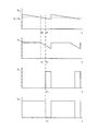
以下に、バイアス設定回路100の動作について説明する。図4は、キャパシタC32の一端の電位V0と、誤差増幅器130から出力される誤差電圧VEと、インバータINV12から出力される制御信号V1と、インバータINV11から出力される信号V2との各タイミングチャートを示す図である。
Hereinafter, the operation of the
電位V0が参照電圧VT−VXよりも大きい期間(時間t0まで)においては、誤差増幅器130は所定値に飽和した正の誤差電圧VEを出力する(第1フェーズ)。この正の誤差電圧VEは、インバータINV12にとって論理レベル“H”の入力信号である。よって、その期間においては、インバータINV12は論理レベル“L”の制御信号V1を出力し、インバータINV11は論理レベル“H”の信号V2を出力する。これにより、NMOSトランジスタM32およびM34がONとなり、バイアス電圧源110のバイアス電圧VTがキャパシタC31に与えられ、キャパシタC31の電位はバイアス電圧VTとなる。
During a period in which the potential V 0 is greater than the reference voltage V T −V X (until time t 0 ), the
キャパシタC32はNMOSトランジスタM30のリーク電流によって放電されるため、その電位V0は徐々に低下し、ついには参照電圧VT−VXよりも小さくなる(第2フェーズ)。すなわち、誤差増幅器130から出力される誤差電圧VEは、正に飽和した値から徐々に低下し、最終的にインバータINV12にとって論理レベル“L”の入力信号となる(時間t1:第3フェーズ)。これにより、インバータINV12は論理レベル“H”の制御信号V1を出力し、インバータINV11は論理レベル“L”の信号V2を出力する。これにより、NMOSトランジスタM31およびM33がONとなり、キャパシタC31の電位VTがキャパシタC32に与えられる。すなわち、キャパシタC32の電位V0は、参照電圧VT−VXよりも大きい電位VTにほぼ一致し、上記した第1フェーズの状態となる。以降、上記第1〜第3フェーズが繰り返される。
Since the capacitor C32 is discharged by the leakage current of the NMOS transistor M30, the potential V 0 gradually decreases and finally becomes smaller than the reference voltage V T −V X (second phase). That is, the error voltage V E output from the
上記した繰り返しフェーズにおいて、制御信号V1の遷移に注目すると、制御信号V1は、定期的に発生するパルスとなっている。整流回路200は、この制御信号V1に同期して動作し、且つ、バイアス設定回路100のダミー整流部とダミースイッチング部とは整流回路200の整流部とスイッチング部とを模擬している。よって、バイアス設定回路100によって、整流回路200の整流部のキャパシタC12およびC22に最適なタイミングによって無駄なく充電することができ、整流部を構成するNMOSトランジスタM1およびM2を常に一定値以上の電圧でバイアスすることができる。換言すれば、整流回路200の利得を常に一定値以上に維持させることができる。
In repeating phases described above, when attention is paid to the transition of the control signal V 1, the control signal V 1 was, has become a regular occurrence pulse. The
なお、上述した例では、MOSトランジスタとして、NMOSトランジスタを用いたが、PMOSトランジスタを用いても良い。 In the above example, an NMOS transistor is used as the MOS transistor, but a PMOS transistor may be used.
以上に説明したように、実施の形態1にかかる高利得整流回路によれば、整流回路200のNMOSトランジスタM1およびM2をバイアスするキャパシタC12およびC22を、バイアス設定回路100によって間接的に監視し、その監視結果に基づいて、キャパシタC12およびC22の充電タイミングを指示する制御信号V1を生成するので、無駄な充電動作が低減され、消費電力の低下を実現することができる。また、キャパシタC12およびC22に与えられるバイアス電圧VTおよびバイアス設定回路100で用いられる参照電圧VT−VXは、NMOSトランジスタM1およびM2の特性を考慮して設計された別のNMOSトランジスタの閾値電圧に基づいて生成されるので、高利得整流回路の製造ばらつきに影響されず、常に一定値以上の利得を有する整流を実現することができる。
As described above, according to the high gain rectifier circuit according to the first embodiment, the capacitors C12 and C22 that bias the NMOS transistors M1 and M2 of the
(実施の形態2)
実施の形態2にかかる高利得整流回路は、実施の形態1にかかる高利得整流回路に対し、初期設定機能を追加したことを特徴としている。
(Embodiment 2)
The high gain rectifier circuit according to the second embodiment is characterized in that an initial setting function is added to the high gain rectifier circuit according to the first embodiment.
図1に示したバイアス設定回路100において、高利得整流回路の初期状態においては、キャパシタC32の電位は参照電圧VT−Vxより十分小さい可能性がある。この場合、キャパシタC31の電荷がキャパシタC32に転送されたとしても、キャパシタC32の電位VOは依然として参照電圧VT−Vxより小さい場合がある。すなわち、図4に示した繰り返しフェーズに基く動作は、上記した第3フェーズに移行せず、制御信号V1のパルスが生成されなくなる。この状態を防止するため、実施の形態2では、キャパシタC32に強制的にバイアス電圧VTを与えるバイアス電圧バイパス部がバイアス設定回路に設けられている。
In the
図5は、実施の形態2にかかる高利得整流回路のバイアス設定回路を示す回路図である。なお、図5において、図1に示したバイアス設定回路100と共通する部分には同一の符号を付し、その説明を省略する。
FIG. 5 is a circuit diagram illustrating a bias setting circuit of the high gain rectifier circuit according to the second embodiment. In FIG. 5, parts common to the
図5に示すバイアス設定回路300において、上記したバイアス電圧バイパス部は、NMOSトランジスタM41およびM42から構成される。NMOSトランジスタM41は、ソース端子がバイアス電圧源110の正極端子に接続され、ドレイン端子がキャパシタC32の一端(プラスライン側)に接続されている。また、NMOSトランジスタM42は、ソース端子がバイアス電圧源110の負極端子に接続され、ドレイン端子がキャパシタC32の他端(マイナスライン側)に接続されている。NMOSトランジスタM41のゲート端子とNMOSトランジスタM42のゲート端子はともに、初期化端子T300に接続されている。初期化端子T300には、初期化信号VCNTが入力される。
In the
以下に、このバイアス設定回路300の動作について説明する。図6は、キャパシタC32の一端の電位V0と、誤差増幅器130から出力される誤差電圧VEと、インバータINV12から出力される制御信号V1と、インバータINV11から出力される信号V2と、初期化信号VCNTの各タイミングチャートを示す図である。
Hereinafter, the operation of the
図6に示すように、初期化信号VCNTを示すパルスが入力された際、すなわち初期化信号VCNTが論理レベル“H”を示す期間(時間t0−t1)においては、NMOSトランジスタM41およびM42はONとなり、バイアス電圧源110から供給されるバイアス電圧VTは、ダミースイッチング部を経由することなく、キャパシタC32に与えられる。すなわち、キャパシタC32の電位V0は、バイアス電圧VTに一致する。この状態から、初期化信号VCNTを示すパルスの立ち下がり後、すなわち初期化信号VCNTが論理レベル“L”を示すと、上述した第1フェーズに移行する。キャパシタC32の電位V0がバイアス電圧VTに一致している期間(時間t0−t1)においては、インバータINV11から出力される信号V2は論理レベル“H”を示しているため、NMOSトランジスタM32およびM34はONとなり、キャパシタC31に対してもバイアス電圧VTが与えられる。これは、第1フェーズ以降の第2および第3フェーズの動作が実行されることを意味する。
As shown in FIG. 6, when a pulse indicating the initialization signal V CNT is inputted, that is, in a period (time t 0 -t 1 ) in which the initialization signal V CNT shows the logic level “H”, the NMOS transistor M 41 And M42 are turned ON, and the bias voltage V T supplied from the
以上に説明したバイアス電圧バイパス部は、バイアス設定回路だけでなく整流回路に設けられてもよい。図7は、実施の形態2にかかる高利得整流回路の整流回路を示す回路図である。なお、図7において、図1に示した整流回路200と共通する部分には同一の符号を付し、その説明を省略する。
The bias voltage bypass unit described above may be provided not only in the bias setting circuit but also in the rectifier circuit. FIG. 7 is a circuit diagram of a rectifier circuit of the high gain rectifier circuit according to the second embodiment. In FIG. 7, the same reference numerals are given to portions common to the
図7に示す整流回路400において、上記したバイアス電圧バイパス部は、NMOSトランジスタM51〜M54から構成される。NMOSトランジスタM51は、ソース端子がバイアス電圧源210の正極端子に接続され、ドレイン端子がキャパシタC12の一端(第1のプラスライン側)に接続されている。また、NMOSトランジスタM52は、ソース端子がバイアス電圧源210の負極端子に接続され、ドレイン端子がキャパシタC12の他端(第1のマイナスライン側)に接続されている。また、NMOSトランジスタM53は、ソース端子がバイアス電圧源210の正極端子に接続され、ドレイン端子がキャパシタC22の一端(第2のプラスライン側)に接続されている。また、NMOSトランジスタM54は、ソース端子がバイアス電圧源210の負極端子に接続され、ドレイン端子がキャパシタC22の他端(第2のマイナスライン側)に接続されている。NMOSトランジスタM51〜M54の各ゲート端子は、初期化端子T400に接続されている。この初期化端子T400には、上記した初期化信号VCNTが入力される。
In the
この整流回路400のバイアス電圧バイパス部によって、整流回路400は、図6に示したタイミングチャートと同様な初期動作を示す。すなわち、初期化信号VCNTが入力されることにより、整流部のキャパシタC12およびC22と、スイッチング部のキャパシタC11およびC21に対して、バイアス電圧源210から供給されるバイアス電圧VTが与えられる。
Due to the bias voltage bypass unit of the
初期化信号VCNTは、高利得整流回路の起動時等における電源検出によって生成することができる。図8は、初期化信号VCNTを生成する電源検出回路を示す回路図である。図8に示す電源検出回路500は、キャパシタC501と、PMOSトランジスタM501およびNMOSトランジスタM502によって構成される第1のCMOSインバータと、PMOSトランジスタM503およびNMOSトランジスタM504によって構成される第2のCMOSインバータと、プルダウン抵抗R1とを備えている。キャパシタC501の一端とPMOSトランジスタM501およびPMOSトランジスタM503の各ソース端子とは、電源VDDに接続されている。NMOSトランジスタM502およびM504の各ドレイン端子は接地されている。キャパシタC501の他端は、第1のCMOSインバータの入力端子、すなわちPMOSトランジスタM501およびNMOSトランジスタM502の各ゲート端子に接続されている。第1のCMOSインバータの出力端子、すなわちPMOSトランジスタM501およびNMOSトランジスタM502の各ドレイン端子は、第2のCMOSインバータの入力端子、すなわちPMOSトランジスタM503およびNMOSトランジスタM504の各ゲート端子に接続されている。第2のCMOSインバータの出力端子、すなわちPMOSトランジスタM503およびNMOSトランジスタM504の各ドレイン端子は、初期化信号VCNTが出力される出力端子に接続されている。また、プルダウン抵抗R1は、NMOSトランジスタM502のゲート端子と接地ラインとの間に接続されている。
The initialization signal V CNT can be generated by detecting the power source when the high gain rectifier circuit is started up. FIG. 8 is a circuit diagram showing a power supply detection circuit that generates the initialization signal VCNT . A power
以下に、この電源検出回路500の動作について説明する。図9は、電源電圧VDDと、キャパシタC501の他端の電位VINT(図8のノードN1の電位)と、生成される初期化信号VCNTとの各タイミングチャートを示す図である。高利得整流回路の起動等によって電源電圧VDDが生じると、その電源電圧VDDの立ち上がりにともなってキャパシタC501が充電される(時間t1まで)。その立ち上がりの間、第1のCMOSインバータの入力端子の電位VINTも上昇し、NMOSトランジスタM502の閾値電圧Vthに達した際に(時間t0)、第1のCMOSインバータにより論理レベル“H”の信号として認識される。これにより、第1のCMOSインバータは、論理レベル“L”の信号を出力し、第2のCMOSインバータは論理レベル“H”の初期化信号VCNTを出力する。キャパシタC501の充電が完了した後(時間t1以降)は、電位VINTはプルダウン抵抗R1を介して徐々に接地電位へと低下し、ついにはNMOSトランジスタM502の閾値電圧Vthよりも小さくなる(時間t2)。これにより、第1のCMOSインバータは、論理レベル“H”の信号を出力し、第2のCMOSインバータは論理レベル“L”の初期化信号VCNTを出力する。以上の動作により、電源検出回路500は、高利得整流回路の起動時に、パルス状の初期化信号VCNTを生成することができる。
Hereinafter, an operation of the power
以上に説明したように、実施の形態2にかかる高利得整流回路によれば、監視対象となるバイアス設定回路300のキャパシタC32と、繰り返し動作においてキャパシタC32にバイアス電圧VTを与えるキャパシタC31とに対して、初期値としてバイアス電圧VTを与えることができる。
As described above, according to the high gain rectifier circuit according to the second embodiment, the capacitor C32 of the
(実施の形態3)
実施の形態3にかかる高利得整流回路は、実施の形態1または実施の形態2において説明した整流回路を複数個備え、且つそれらが縦続接続された構成を採用した回路であり、特にその縦続接続によって生じる新たな懸念に対処するものである。まずは、その新たな懸念について説明する。ここでは、縦続接続される整流回路(以下、縦続整流回路と称する)として、実施の形態1で説明した整流回路200を例に挙げる。
(Embodiment 3)
The high-gain rectifier circuit according to the third embodiment is a circuit that includes a plurality of rectifier circuits described in the first or second embodiment and that employs a configuration in which they are cascade-connected. Addressing new concerns arising from First, I will explain the new concerns. Here, the
図10は、縦続整流回路の例を示す回路図である。図10に示す縦続整流回路600は、縦続接続されたn個の整流回路ブロック200−1〜200−nと、バイアス電圧源610と、インバータINV1およびINV2と、逆流防止回路630と、バッテリ660と、を備える。整流回路ブロック200−1〜200−nのそれぞれは、図1に示した整流回路200の構成要素のうち、上述した整流部と、トランスファゲートとして機能する8つのNMOSトランジスタとを備える。隣接する整流回路ブロック間において、一方の整流回路ブロックの整流部のプラス端子と他方の整流回路ブロックの整流部のマイナス端子とが接続され、トランスファゲート群のゲート端子に接続される2つの信号ラインがそれぞれ共有されている。バイアス電源610は、図1に示したバイアス電源210に相当し、整流回路ブロック200−1〜200−nにおいて共有される。
FIG. 10 is a circuit diagram illustrating an example of a cascade rectifier circuit. The
図10では、整流回路ブロック200−1〜200−nのうち、最下段の整流ブロック200−1の回路構成のみが具体的に示されている。NMOSトランジスタM1−1,M2−1,M11−1〜M14−1,M21−1〜M24−1と,キャパシタC1−1,C2−1,C11−1,C12−1,C21−1,C22−1は、それぞれ図1のNMOSトランジスタM1,M2,M11〜M14,M21〜M24と,キャパシタC1,C2,C11,C12,C21,C22に相当する。図10に示すインバータINV1およびINV2もまた整流回路ブロック200−1〜200−nにおいて共有され、図1のインバータINV1およびINV2と同様に機能する。 FIG. 10 specifically shows only the circuit configuration of the lowermost rectifying block 200-1 among the rectifying circuit blocks 200-1 to 200-n. NMOS transistors M1-1, M2-1, M11-1 to M14-1, M21-1 to M24-1, and capacitors C1-1, C2-1, C11-1, C12-1, C21-1, C22- 1 corresponds to the NMOS transistors M1, M2, M11 to M14, M21 to M24 and capacitors C1, C2, C11, C12, C21, and C22 of FIG. Inverters INV1 and INV2 shown in FIG. 10 are also shared by rectifier circuit blocks 200-1 to 200-n and function in the same manner as inverters INV1 and INV2 in FIG.
バッテリ660は、電源電圧VDDを生成する電源であり、ここでは二次電池を想定している。このバッテリ660は、逆流防止回路630を介して、最上段の整流回路ブロック200−nの整流部のプラス端子に接続される。すなわち、整流回路ブロック200−1〜200−nによって整流された電圧は、バッテリ660に蓄積される。なお、逆流防止回路630は、例えば、バッテリ660に接続される端子側をカソードとしたダイオードである。
The
図10に示すとおり、整流回路ブロック200−1〜200−nの各整流部を構成するNMOSトランジスタは、バッテリ660から接地ラインに至るライン上において直列に接続されているため、各々において生じたリーク電流の大きさは互いに等しい。換言すれば、整流回路ブロック200−1〜200−n間において、整流部において生じるリーク電流の大きさに差異はない。よって、図1に示したバイアス設定回路100によっても、この縦続整流回路600において生じた整流部のリーク電流を正確に模擬することができる。
As shown in FIG. 10, the NMOS transistors constituting the rectifiers of the rectifier circuit blocks 200-1 to 200-n are connected in series on the line from the
つぎに、この縦続整流回路600において、最下段の整流回路ブロック200−1に注目してみる。今、キャパシタC12−1およびC22−1の両端の電圧が、バイアス電圧源610から供給されるバイアス電圧VT(実施の形態1において定義)に一致しているとすると、NMOSトランジスタM11−1,M13−1,M21−1,M23−1はOFFである。この状態において、信号入力端子TA、すなわち整流部のNMOSトランジスタM1−1とM2−1の接続点に微少な交流信号が入力された場合、その接続点はNMOSトランジスタM2−1のソース端子とほぼ同じ電位、すなわち、ほぼ接地電位を示す。よって、NMOSトランジスタM1−1のゲート端子の電位は、キャパシタC12−1の両端の電圧VTと同じ値を示す。
Next, in the
NMOSトランジスタM1−1のゲート端子は、トランスファーゲートの一つであるNMOSトランジスタM11−1のドレイン端子に接続されているため、NMOSトランジスタM11−1のドレイン端子もまた電位VTを示す。一方、NMOSトランジスタM11−1のソース端子は、NMOSトランジスタM11−1との相補動作によりON状態となっているNMOSトランジスタ12−1を介して、バイアス電圧源610の正極端子と同じ電位、すなわちバイアス電圧VTに一致する。従って、NMOSトランジスタM11−1のソース−ドレイン間に電位差は生じず、そのNMOSトランジスタM11−1のリーク電流も無視できる程度となる。
The gate terminal of the NMOS transistor M1-1 is because it is connected to the drain terminal of the NMOS transistor M11-1 is one of the transfer gates, also shows the potential V T drain terminal of the NMOS transistor M11-1. On the other hand, the source terminal of the NMOS transistor M11-1 has the same potential as the positive terminal of the
同じ状態において、NMOSトランジスタM13−1,M21−1,M23−1の各ソース−ドレイン間電圧もほぼ0であり、これらNMOSトランジスタのリーク電流についても無視できる。この状態は、整流ブロック200−nについてもほぼ同様になる。 In the same state, the source-drain voltages of the NMOS transistors M13-1, M21-1, and M23-1 are almost zero, and the leakage currents of these NMOS transistors can be ignored. This state is substantially the same for the rectifying block 200-n.
つづいて、入力信号が大きい場合で、しかも、バイアス電圧源610に充電される場合について、最上段の整流回路ブロックの状態について考える。図11は、図10と同じ縦続整流回路600を示すが、整流回路ブロック200−1〜200−nのうち、最上段の整流ブロック200−nの回路構成のみが具体的に示されている。図11において、NMOSトランジスタM1−n,M2−n,M11−n〜M14−n,M21−n〜M24−nと,キャパシタC1−n,C2−n,C11−n,C12−n,C21−n,C22−nは、それぞれ図1のNMOSトランジスタM1,M2,M11〜M14,M21〜M24と,キャパシタC1,C2,C11,C12,C21,C22に相当する。
Next, the state of the uppermost rectifier circuit block will be considered when the input signal is large and the
今、キャパシタC12−nおよびC22−nの両端の電圧が、バイアス電圧源610から供給されるバイアス電圧VTに一致しているとすると、NMOSトランジスタM11−n,M13−n,M21−n,M23−nはOFFである。この状態において、信号入力端子TA、すなわち整流部のNMOSトランジスタM1−nとM2−nの接続点にバイアス電圧源610に十分充電できる大きな信号が入力された場合、その接続点は、整流回路ブロック200−1〜200−(n−1)の各平滑キャパシタC2−1〜C2−(n−1)の両端の電圧の和にほぼ等しい。逆流防止回路630の入出力端子間の電圧は非常に小さいため、それを無視すると、この接続点の電位は、バッテリ660に充電すべき電源電圧VDDとほぼ一致する。よって、NMOSトランジスタM1−nのゲート端子の電位は、キャパシタC12−nの両端の電圧VTに電源電圧VDDを加算した電圧VT+VDDと同じ値を示す。
Now, assuming that the voltages at both ends of the capacitors C12-n and C22-n coincide with the bias voltage V T supplied from the
NMOSトランジスタM1−nのゲート端子は、トランスファーゲートの一つであるNMOSトランジスタM11−nのドレイン端子に接続されているため、NMOSトランジスタM11−nのドレイン端子もまた電位VT+VDDを示す。一方、NMOSトランジスタM11−nのソース端子は、NMOSトランジスタM11−nとの相補動作によりON状態となっているNMOSトランジスタ12−nを介して、バイアス電圧源610の正極端子と同じ電位、すなわちバイアス電圧VTに一致する。従って、NMOSトランジスタM11−nのソース−ドレイン間には電位差VDDが生じる。この電位差VDDは、キャパシタC12−nの電荷をキャパシタC11−nへと転送させる要因となる。同じ状態において、NMOSトランジスタM13−nの各ソース−ドレイン間電圧もほぼVDDでありリーク電流が流れる。よって、整流部のNMOSトランジスタM1−nに接続されたキャパシタC12−nは、トランスファーゲートであるNMOSトランジスタM11−nのリーク電流によっても放電してしまう。同様な理由により、整流部のNMOSトランジスタM2−nに接続されたキャパシタC22−nもまた、トランスファーゲートであるNMOSトランジスタM21−nのリーク電流によって放電してしまう。
Since the gate terminal of the NMOS transistor M1-n is connected to the drain terminal of the NMOS transistor M11-n, which is one of the transfer gates, the drain terminal of the NMOS transistor M11-n also exhibits the potential V T + V DD . On the other hand, the source terminal of the NMOS transistor M11-n has the same potential as the positive terminal of the
ところが、図1に示したバイアス設定回路100は、これらトランスファーゲートのリーク電流の発生を模擬していない。すなわち、バイアス設定回路100は、図10に示した縦続整流回路600の整流部のキャパシタの電位状態を正確に監視することはできない。実施の形態3にかかる高利得整流回路は、この問題を解決したバイアス設定回路を備えたことを特徴としている。
However, the
図12は、実施の形態3にかかる高利得整流回路を構成するバイアス設定回路を示す回路図である。なお、図12において、図1のバイアス回路100と共通する部分には同一の符号を付し、その説明を省略する。
FIG. 12 is a circuit diagram of a bias setting circuit constituting the high gain rectifier circuit according to the third embodiment. In FIG. 12, parts common to the
図12に示すバイアス設定回路700は、直列接続された2つのNMOSトランジスタM61およびM62と電流源710とを備えた点が図1のバイアス設定回路100と異なる。また、誤差増幅器130の逆相入力端子IN2に接続される参照電圧源720が参照電圧VDD−VT−VXを生成する点と、ダミー整流部のNMOSトランジスタM30のドレイン端子およびソース端子が接地されていない点も異なる。
A
NMOSトランジスタM61およびM62は、ゲート端子とドレイン端子とが互いに接続された負荷素子として機能し、図12では、NMOSトランジスタM61のソース端子とNMOSトランジスタM62のドレイン端子とが互いに接続されている。NMOSトランジスタM61のドレイン端子は電源ライン(電源電圧VDD)に接続され、NMOSトランジスタM62のソース端子はNMOSトランジスタM30のドレイン端子およびソース端子に接続されている。電流源710もまたNMOSトランジスタM30のドレイン端子およびソース端子に接続されている。この構成によって、NMOSトランジスタM61およびM62は、電流源710から供給される微少電流によって、電源ラインとNMOSトランジスタM30との間に各NMOSトランジスタM61およびM62の閾値電圧の和とほぼ同じ電圧降下を与える。特に、これらNMOSトランジスタM61およびM62は、その閾値電圧が、バイアス電圧源110および210が生成するバイアス電圧VTに等しくなるようなトランジスタである。よって、NMOSトランジスタM30のドレイン端子およびソース端子には、電位VDD−2VTが与えられている。なお、電流源710は、一般に用いられるバイアス回路を用いてもよいが、ゲート−ソース間電圧を0Vに設定したトランジスタで構成し、そのリーク電流を利用してもよい。
The NMOS transistors M61 and M62 function as a load element in which the gate terminal and the drain terminal are connected to each other. In FIG. 12, the source terminal of the NMOS transistor M61 and the drain terminal of the NMOS transistor M62 are connected to each other. The drain terminal of the NMOS transistor M61 is connected to the power supply line (power supply voltage V DD ), and the source terminal of the NMOS transistor M62 is connected to the drain terminal and the source terminal of the NMOS transistor M30. The
キャパシタC32の両端の電圧がバイアス電圧VTと一致した状態では、トランスファーゲートであるNMOSトランジスタM31のドレイン端子は、NMOSトランジスタM30のドレイン端子およびソース端子の電位VDD−2VTよりバイアス電圧VTだけ高い電位VDD−VTを示す。一方、NMOSトランジスタM31のソース端子は、NMOSトランジスタM31との相補動作によりON状態となっているNMOSトランジスタ32を介して、バイアス電圧源110の正極端子と同じ電位、すなわちバイアス電圧VTに一致する。従って、NMOSトランジスタM31のソース−ドレイン間には電位差VDD−2VTが生じる。この電位差VDD−2VTは、キャパシタC32の放電の要因となる。すなわち、図11に示した最上段の整流回路ブロック200−nと同様な電流リーク状態を実現することができる。
In a state in which the voltage across the capacitor C32 coincides with the bias voltage V T , the drain terminal of the NMOS transistor M31 serving as the transfer gate is bias voltage V T from the potential V DD -2V T of the drain terminal and source terminal of the NMOS transistor M30. Shows a higher potential V DD -V T. On the other hand, the source terminal of the NMOS transistor M31 coincides with the same potential as the positive terminal of the
但し、このNMOSトランジスタM31のソース−ドレイン間電圧VDD−2VTは、整流回路ブロック200−nのNMOSトランジスタM11−nのソース−ドレイン間電圧VDDよりも2VTだけ小さい。よって、正確には、このバイアス設定回路700によっても縦続整流回路600の電流リーク状態を模擬していないことになる。しかしながら、この2VTの差は、NMOSトランジスタM31の寸法を調整することによって無視することができる。一般に、ゲート端子が接地されたNMOSトランジスタのリーク電流はドレイン−ソース間電圧(VDS)に依存する。その依存性はトランジスタのプロセス条件に応じて決まる。NMOSトランジスタM31のVDS依存性が小さい場合は、そのVDSによって生じるリーク電流も小さい。一方、NMOSトランジスタM31のVDS依存性が大きい場合には、例えば、誤差電圧2VTによって数倍リーク電流が変わる。そこで、NMOSトランジスタM31およびM33の寸法を、縦続整流回路600の各トランスファーゲートに比べて、例えば1〜10倍の間に大きく設定する。これにより、バイアス設定回路700において、縦続整流回路600の電流リーク状態を模擬することができる。
However, the source-drain voltage V DD -2V T of the NMOS transistor M31 is smaller than the source-drain voltage V DD of the NMOS transistor M11-n of the rectifier circuit block 200-n by 2V T. Therefore, precisely, the
バイアス設定回路700の動作は、参照電圧源720において、キャパシタC32の電位V0と比較される参照電圧がVDD−VT−VXとなる点以外は、図4に示したタイミングチャート通りであるので、ここではその説明を省略する。
The operation of the
なお、縦続整流回路600では、最上段の整流回路ブロック200−n以外の整流回路ブロック200−2〜200−(n−1)でも、トランスファーゲートにリーク電流が生じる可能性があるが、最も大きなリーク電流はやはり最上段の整流回路ブロック200−nにおいて生じる。よって、バイアス設定回路700は、上述したように、最上段の整流回路ブロック200−nのトランスファーゲートのドレイン−ソース間電圧VDDの生成を模擬するのが最も有効である。
In the
以上に説明したように、実施の形態3にかかる高利得整流回路によれば、縦続整流回路600の最上段の整流回路ブロック200−nにおいて生じるトランスファーゲートの電流リークを、バイアス設定回路700によって模擬できるので、縦続整流回路600に対しても実施の形態1と同様な効果を享受することができる。
As described above, according to the high gain rectifier circuit of the third embodiment, the
(実施の形態4)
実施の形態4にかかる高利得整流回路は、実施の形態3において説明した問題を別の方法によって解決したバイアス設定回路を備えたことを特徴としている。図13は、実施の形態4にかかる高利得整流回路を構成するバイアス設定回路を示す回路図である。なお、図13において、図1のバイアス回路100と共通する部分には同一の符号を付し、その説明を省略する。
(Embodiment 4)
The high gain rectifier circuit according to the fourth embodiment is characterized by including a bias setting circuit that solves the problem described in the third embodiment by another method. FIG. 13 is a circuit diagram showing a bias setting circuit constituting the high gain rectifier circuit according to the fourth embodiment. In FIG. 13, parts common to the
図13に示すバイアス設定回路800は、3つの直列接続されたPMOSトランジスタM71、PMOSトランジスタM73、およびNMOSトランジスタM72と、電流源810と、遅延回路830と、EXOR回路840と、AND回路850とを備えた点が図1のバイアス回路100と異なる。また、誤差増幅器130の逆相入力端子IN2に接続される参照電圧源820が参照電圧VDD−VXを生成する点と、ダミー整流部のNMOSトランジスタM30のドレイン端子およびソース端子が接地されていない点も異なる。
13 includes three PMOS transistors M71, PMOS transistors M73, and NMOS transistors M72, a
PMOSトランジスタM71およびNMOSトランジスタM72は、CMOSインバータとして機能し、図13では、PMOSトランジスタM71のソース端子は電源ライン(電源電圧VDD)に接続され、NMOSトランジスタM72のソース端子は接地ラインに接続されている。NMOSトランジスタM73は、ゲート端子とドレイン端子とが共にPMOSトランジスタM71のドレイン端子に接続され、ソース端子がNMOSトランジスタM72のドレイン端子に接続されている。NMOSトランジスタM72とNMOSトランジスタM73の接続点は、ダミー整流部のNMOSトランジスタM30のドレイン端子およびソース端子に接続されており、上記したCMOSインバータの出力点としても機能する。PMOSトランジスタM71のゲート端子とNMOSトランジスタM72のゲート端子は互いに接続され、上記したCMOSインバータの入力点として機能する。 The PMOS transistor M71 and the NMOS transistor M72 function as a CMOS inverter. In FIG. 13, the source terminal of the PMOS transistor M71 is connected to the power supply line (power supply voltage V DD ), and the source terminal of the NMOS transistor M72 is connected to the ground line. ing. The NMOS transistor M73 has both a gate terminal and a drain terminal connected to the drain terminal of the PMOS transistor M71, and a source terminal connected to the drain terminal of the NMOS transistor M72. The connection point of the NMOS transistor M72 and the NMOS transistor M73 is connected to the drain terminal and the source terminal of the NMOS transistor M30 of the dummy rectification unit, and also functions as an output point of the above-described CMOS inverter. The gate terminal of the PMOS transistor M71 and the gate terminal of the NMOS transistor M72 are connected to each other and function as an input point of the above-described CMOS inverter.
このCMOSインバータの入力点はAND回路850の出力端子(信号Vc)に接続され、AND回路850は、インバータINV12の出力(すなわち制御信号V1)とEXOR回路840の出力(信号Vb)を入力する。EXOR回路840は、インバータINV12の出力と遅延回路830の出力(信号Va)を入力する。遅延回路830は、インバータINV12の出力を時間τだけ遅延させた信号Vaを出力する。
The input point of this CMOS inverter is connected to the output terminal (signal V c ) of the AND
以下に、バイアス設定回路800の動作について説明する。図14は、インバータINV12から出力される制御信号V1と、遅延回路830から出力される信号Vaと、EXOR回路840から出力される信号Vbと、AND回路850から出力される信号Vcと、キャパシタC32の一端の電位V0と、キャパシタC32の他端の電位V3との各タイミングチャートを示す図である。
Hereinafter, the operation of the
ここでは、初期状態として、制御信号V1が論理レベル“L”から“H”に遷移した直後を考える。この状態において、遅延回路830は時間τの計測時を開始し、時間τが経過するまでその出力信号Vaは論理レベル“L”を示す。よって、制御信号V1が論理レベル“L”から“H”に遷移してから時間τが経過するまでの間は、図14に示すように、信号Vbおよび信号Vcは、ともに論理レベル“H”を示す。従って、PMOSトランジスタM71とNMOSトランジスタM72の各ゲートには論理レベル“H”の信号が入力され、それを反転した論理レベル“L”の信号がNMOSトランジスタM72とPMOSトランジスタM73の接続点から出力される。この論理レベル“L”の信号は、ほぼ0V(接地電位GND)であるため、キャパシタC32の他端の電位V3もGNDを示す。この間、キャパシタC32の一端の電位V0は、電位V3よりもバイアス電圧VTだけ高い値、すなわち電位VTと一致する。
Here, as an initial state, immediately after the control signal V 1 transitions from the logic level “L” to “H” is considered. In this state, the
なお、時間τは、少なくともキャパシタC31からNMOSトランジスタM31およびM33を介してキャパシタC32へと電荷の転送が完了するまでに要する時間である。時間τが経過すると、遅延回路830の出力信号Vaは論理レベル“H”を示す。信号Vbは論理レベル“H”のままであるが、信号Vcは論理レベル“L”を示す。従って、PMOSトランジスタM71とNMOSトランジスタM72の各ゲートには論理レベル“L”の信号が入力され、それを反転した論理レベル“H”の信号がNMOSトランジスタM72とNMOSトランジスタM73の接続点から出力される。この論理レベル“H”の信号は、正確には、電源電圧VDDからNMOSトランジスタM73の閾値電圧VTだけ降下した電位VDD-VTを有する。すなわち、キャパシタC32の他端の電位V3もVDD-VTを示す。この間、キャパシタC32の一端の電位V0は、電位V3よりもバイアス電圧VTだけ高い値、すなわち電位VDDと一致する。誤差増幅器130は、この電位VDDと参照電圧VDD−VXの差分VXを出力する。この差分VXは、図4に示したタイミングチャートと同様に、インバータINV12によって論理レベル“H”と認識され、結果的に制御信号V1の論理レベルを“H”から“L”に変化させる。論理レベル“L”の制御信号V1は、NMOSトランジスタM31およびM33をOFFにし、インバータINV11を介してNMOSトランジスタM32およびM34をONにする。この状態では、電位V0は、電源電圧VDDと一致するため、NMOSトランジスタM31のドレイン−ソース間電圧はVDD-VTとなり、NMOSトランジスタM31による電流リークの発生が実現される。この電流リークによって、キャパシタC32の電位V0は徐々に低下し、ついには参照電圧VDD−VXよりも小さくなる。すなわち、誤差増幅器130から出力される誤差電圧VEは、インバータINV12にとって論理レベル“L”の入力信号となる。これにより、再度、制御信号V1が初期状態と同様に論理レベル“H”を示す。以降、上記したフェーズが繰り返される。
The time τ is a time required for completing the transfer of charges from at least the capacitor C31 to the capacitor C32 via the NMOS transistors M31 and M33. When the time τ elapses, the output signal Va of the
すなわち、実施の形態1と同様に、整流回路の整流部のキャパシタの状態を監視することができる。特に、実施の形態4では、NMOSトランジスタM31による電流リーク状態をドレイン−ソース間電圧VDD−VXによって実現している。この電圧は、実施の形態3で示したドレイン−ソース間電圧VDD−2VXよりも電圧VXだけVDDに近づいている。換言すれば、これは、縦続整流回路の最上段の整流回路ブロックで電流リークの要因となっているドレイン−ソース電圧VDDにより近い値であり、実施の形態3に示したバイアス設定回路700よりも高精度に縦続整流回路600の電流リーク状態を模擬することができる。
That is, as in the first embodiment, the state of the capacitor of the rectifier unit of the rectifier circuit can be monitored. In particular, in the fourth embodiment, the current leakage state by the NMOS transistor M31 is realized by the drain-source voltage V DD -V X. This voltage is closer to V DD by the voltage V X than the drain-source voltage V DD -2V X shown in the third embodiment. In other words, this is a value closer to the drain-source voltage V DD that causes current leakage in the uppermost rectifier circuit block of the cascade rectifier circuit, which is more than the
(実施の形態5)
実施の形態5にかかる高利得整流回路は、実施の形態3において説明した問題をさらに別の方法によって解決したバイアス設定回路を備えたことを特徴としている。図15は、実施の形態5にかかる高利得整流回路を構成するバイアス設定回路を示す回路図である。なお、図15において、図1のバイアス回路100と共通する部分には同一の符号を付し、その説明を省略する。
(Embodiment 5)
The high gain rectifier circuit according to the fifth embodiment is characterized by including a bias setting circuit that solves the problem described in the third embodiment by another method. FIG. 15 is a circuit diagram showing a bias setting circuit constituting the high gain rectifier circuit according to the fifth embodiment. In FIG. 15, parts common to those of the
図15に示すバイアス設定回路900は、NMOSトランジスタM81を備えた点が図1のバイアス設定回路100と異なる。また、誤差増幅器130の逆相入力端子IN2にキャパシタC32の一端(電位V0)が接続され、正相入力端子IN1にバイアス電圧源110の正極端子が接続されている点も異なる。さらに、これに伴い、参照電圧源120も排除されている。
A
NMOSトランジスタM81は、ドレイン端子が電源ライン(電源電圧VDD)に接続され、ソース端子がキャパシタC32の一端(電位V0)に接続され、ゲート端子がNMOSトランジスタM30のドレイン端子およびソース端子にゲート端子に接続されている。 The NMOS transistor M81 has a drain terminal connected to the power supply line (power supply voltage V DD ), a source terminal connected to one end (potential V 0 ) of the capacitor C32, and a gate terminal connected to the drain terminal and the source terminal of the NMOS transistor M30. Connected to the terminal.
この回路では、NMOSトランジスタM81は、ゲート端子に接地電位が入力されているため常にOFFであり、そのドレイン−ソース間電圧は電源電圧VDDから閾値電圧VTを減算したVDD−VTで表される。これは、NMOSトランジスタM31およびM33がOFFである期間に、ドレイン−ソース間電圧VDD−VTによるNMOSトランジスタM81のリーク電流をキャパシタC32の一端(電位V0)に与えることを意味する。換言すれば、実施の形態4において説明したNMOSトランジスタM31のドレイン−ソース間電圧VDD−VTを、NMOSトランジスタM81によって生成している。但し、このリーク電流は、キャパシタC32の放電を誘起するものではなく、逆に、キャパシタC32に流入し、そのキャパシタC32の一端の電位V0を上昇させる。そこで、誤差増幅器130は、正相入力端子IN1にバイアス電圧源110の電圧VTを入力することで、その電位V0の上昇分を検出する。具体的には、例えば、NMOSトランジスタM81のドレイン−ソース間電圧VDD−VTによって、当初バイアス電圧VTを示していた電位V0が電圧VX以上上昇した際、すなわち、VT+VXよりも大きくなった際に、誤差電圧VEの論理レベルが反転する。その点以外は、バイアス設定回路900の動作は、図4に示したタイミングチャート通りであるので、ここではその説明を省略する。なお、上記電圧VXは、図2のNMOSトランジスタM123およびM124の寸法を調節することにより得られる。
In this circuit, the NMOS transistor M81 is always OFF because the ground potential is input to the gate terminal, and the drain-source voltage is V DD −V T obtained by subtracting the threshold voltage V T from the power supply voltage V DD. expressed. This means that the leakage current of the NMOS transistor M81 due to the drain-source voltage V DD -V T is given to one end (potential V 0 ) of the capacitor C32 during the period when the NMOS transistors M31 and M33 are OFF. In other words, the drain-source voltage V DD -V T of the NMOS transistor M31 described in the fourth embodiment is generated by the NMOS transistor M81. However, this leakage current does not induce discharge of the capacitor C32, but conversely flows into the capacitor C32 and raises the potential V 0 at one end of the capacitor C32. Therefore, the
以上に説明したように、実施の形態5にかかる高利得整流回路によれば、縦続整流回路600の最上段の整流回路ブロック200−nにおいて生じるトランスファーゲートの電流リークを、バイアス設定回路900によって模擬できるので、実施の形態1と同様な効果を享受することができる。
As described above, according to the high gain rectifier circuit according to the fifth embodiment, the
(実施の形態6)
実施の形態6にかかる高利得整流回路は、実施の形態5にかかる高利得整流回路の変形例である。図16は、実施の形態6にかかる高利得整流回路を構成するバイアス設定回路を示す回路図である。なお、図16において、図1のバイアス設定回路100と共通する部分には同一の符号を付し、その説明を省略する。
(Embodiment 6)
The high gain rectifier circuit according to the sixth embodiment is a modification of the high gain rectifier circuit according to the fifth embodiment. FIG. 16 is a circuit diagram showing a bias setting circuit constituting the high gain rectifier circuit according to the sixth embodiment. In FIG. 16, parts common to the
図16に示すバイアス設定回路1000は、第2のダミー整流部と第2のダミースイッチング部が追加された点が図1のバイアス設定回路100と異なる。以下、図1のダミー整流部およびダミースイッチング部をそれぞれ第1のダミー整流部および第1のダミースイッチング部と称する。バイアス設定回路1000では、第2のダミー整流部として、第1のダミー整流部のNMOSトランジスタM30およびキャパシタC32にそれぞれ対応するNMOSトランジスタM30’およびキャパシタC32’を備える。また、第2のダミースイッチング部として、第1のダミースイッチング部のNMOSトランジスタM31,M32,M33,M34と,キャパシタC31,C32と、バイアス電圧源110とにそれぞれ対応するNMOSトランジスタM31’,M32’,M33’,M34’と、キャパシタC31’,C32’と、バイアス電圧源110’とを備える。さらに、バイアス設定回路1000は、NMOSトランジスタM91を備え、誤差増幅器130の逆相入力端子IN2にキャパシタC32’の一端(電位V0’)が接続されている点も異なる。また、これに伴い、参照電圧源120が排除されている。
A
NMOSトランジスタM91は、ドレイン端子が電源ライン(電源電圧VDD)に接続され、ソース端子がキャパシタC32’の一端(電位V0’)に接続され、ゲート端子がNMOSトランジスタM30’のドレイン端子およびソース端子にゲート端子に接続されている。 The NMOS transistor M91 has a drain terminal connected to the power supply line (power supply voltage V DD ), a source terminal connected to one end (potential V 0 ′) of the capacitor C32 ′, and a gate terminal connected to the drain terminal and source of the NMOS transistor M30 ′. The terminal is connected to the gate terminal.
このバイアス設定回路1000は、換言すれば、図15の誤差増幅器130の正相入力端子IN1がバイアス電源110の正極端子に接続されることに替えて、正相入力端子IN1が第1のダミー整流部のキャパシタC32の一端(電位V0)に接続された回路構成を有する。
In other words, the
すなわち、バイアス設定回路1000の動作は、実施の形態5において説明したバイアス設定回路900とほぼ同じである。但し、バイアス設定回路1000においては、誤差増幅器120の正相入力端子IN1に入力される参照電圧がバイアス電圧VTそのものではなく、整流部のキャパシタC32の現在の電位としているので、キャパシタC32’へのリーク電流の流入による電圧誤差分をより正確に検出することができるという利点がある。
That is, the operation of the
(実施の形態7)
実施の形態1〜6にかかる高利得整流回路は、RFIDタグの整流回路として用いることができる。実施の形態7では特に実施の形態2にかかる高利得整流回路を用いて構成されたRFIDタグの例を説明する。図17は、実施の形態7にかかるRFIDタグのブロック図である。図17に示すRFIDタグ1010は、アンテナ9と、図5に示したようなバイアス設定回路10と、図7に示したような整流回路20と、逆流防止回路30と、RF検出回路40と、制御回路50と、二次電池であるバッテリ60とを備えて構成される。特に、バイアス設定回路10と整流回路20とによって実施の形態2にかかる高利得整流回路が構成される。また、このRFIDタグ1010は、バッテリ60から供給される電源電圧VDDによって駆動するRFIDタグであり、その動作のために、整流回路20から電源電圧を生成することを必須要件としない。すなわち、バイアス設定回路10と、整流回路20と、逆流防止回路30と、RF検出回路40と、制御回路50とは、バッテリ60から引き伸ばされた電源ラインおよび接地ラインにそれぞれ接続されている。また、この例では、初期化信号VCNTは、図8に示した電源検出回路によって生成されず、制御回路50によって生成されるものとする。
(Embodiment 7)
The high gain rectifier circuit according to the first to sixth embodiments can be used as a rectifier circuit of an RFID tag. In the seventh embodiment, an example of an RFID tag configured using the high gain rectifier circuit according to the second embodiment will be described. FIG. 17 is a block diagram of an RFID tag according to the seventh embodiment. An
アンテナ9は、リーダ/ライタ(図示せず)によって与えられる電界に応じて、そのアンテナ線に交流電流を誘起する。この交流電流は、整流回路20の信号入力端子に入力される。整流回路20は、バッテリ60から供給される電源電圧によって駆動する。よって、図3−1〜図3−4に示したようなバイアス電圧源または参照電圧源は、バッテリ60から供給される電源電圧VDDからバイアス電圧VTまたは参照電圧VT−VXを生成する。すなわち、整流回路20において、アンテナ9から交流電流が入力されるか否かに関係なく、整流回路20の整流部を構成するMOSトランジスタのゲート端子とソース端子との間にはバイアス電圧VTが印加される。よって、整流回路20は、実施の形態1および2に示したように、アンテナ9において誘起された0.7V程度未満の実効値を有する微弱な交流電流をも整流することができる。すなわち、アンテナ9が受け取った微弱なデータ信号を復調することができる。特に、この整流動作においては、実施の形態2に説明したようにバイアス設定回路10から最適なタイミングで制御信号V1が整流回路20に入力されており、整流回路20は、この制御信号V1に基いて、整流部を構成するMOSトランジスタのバイアス電圧を所定値以上に維持する。
The antenna 9 induces an alternating current in the antenna line in accordance with an electric field applied by a reader / writer (not shown). This alternating current is input to the signal input terminal of the
復調されたデータ信号は、RF検出回路40へと入力される。RF検出回路40は、このデータ信号を検出することによって制御回路50を駆動するとともに、検出したデータ信号を制御回路50へと出力する。整流回路20によって得られた直流電圧はまた、充電用電力として、逆流防止回路30を介して、バッテリ60にも供給される。
The demodulated data signal is input to the
制御回路50は、整流回路20から受け取ったデータ信号に基づき、メモリ(図示せず)に格納されたデータ(代表的なものとしてはタグ識別情報)の取り出しやメモリへのデータの書き込みを行なう。制御回路50は、アンテナ9に接続された負荷変調部を備えており、メモリ等から取り出されたデータは、この負荷変調部によるアンテナ9の電流の変調によって、リーダ/ライタに送信される。具体的には、負荷変調部は、アンテナ9の負荷を変化させ、この変化がリーダ/ライタのアンテナを流れる電流を微小に変化させる。この微小な変化が、リーダ/ライタによって検出され、データ信号として認識される。
Based on the data signal received from the
また、制御回路50は、バイアス設定回路10および整流回路20に入力される初期化信号VCNTを生成する。図18は、初期化信号VCNTの生成タイミングを説明するタイミングチャートである。図18に示すように、制御回路50が、自己の動作状態から停止状態になる直前(時間t1)に初期化信号VCNTであるパルスを出力することによって、制御回路50の非動作状態に移行する際に、バイアス設定回路10および整流回路20を初期化することができる。但し、RFIDタグの製造後初めてこのRFIDタグにバッテリ60を接続した際には、制御回路50は動作していないので、図18に従ったタイミングでは初期化信号VCNTは生成されない。しかしながら、RFIDタグ製造時に試験をする際、RFIDタグに強いRF信号を与えることにより、制御回路50を動作させることが可能であり、これにより、初期化信号VCNTを生成することが可能である。換言すれば、製造時試験を行なう前は、バイアス設定回路10および整流回路20からなる構成は高利得整流回路として動作せず、従来どおりの低利得な整流回路として動作し、強いRF信号を与えることにより、それを高利得整流回路として動作させることができる。
In addition, the
以上に説明したRFIDタグは、制御回路50が初期化信号VCNTを生成するとしたが、図8に示した電源検出回路によって初期化信号VCNTを生成してもよい。図19は、電源検出回路を備えたRFIDタグのブロック図である。なお、図19において、図17に示したRFIDタグと共通する部分には同一の符号を付し、その説明を省略する。図19に示すRFID1020タグでは、図8に示したような電源検出回路70を備え、制御回路50に替えてこの電源検出回路70が初期化信号VCNTを生成する。これにより、RFIDタグの製造後初めてこのRFIDタグにバッテリ60を接続した場合であっても、電源検出回路70がそれを検出し、初期化信号VCNTを生成することができる。
In the RFID tag described above, the
また、本実施の形態にかかるRFIDタグは、バッテリを備えているために、RFIDタグに温度センサ、スピーカ、マイク、発光素子などの種々の入出力デバイスを搭載することも容易である。その場合、RFIDタグのさらなる応用の拡大を図ることが可能となる。例えば、RFIDタグにセンサを搭載する場合は、図20のような構成になる。なお、図20において、図17に示したRFIDタグと共通する部分には同一の符号を付し、その説明を省略する。図20に示すRFIDタグ1030では、センサ80はバッテリ60から供給される電源ラインと接地ラインとに接続している。センサ80への信号の送受は例えば制御回路50との間で行う。ここでは、センサの一例として、温度センサを搭載したRFIDタグの例を説明する。リーダ/ライタ(図示せず)から送信が無いとき、温度センサはスリープ状態であり、電流を消費しない。リーダ/ライタから送信信号があり、このセンサ付RFIDタグ1030への信号送信の指令が有った場合、温度センサは起動し、温度を検知してデータを制御回路50へと送出する。この信号データと、RFIDタグの固有データを合わせた信号データをRFIDタグからリーダ/ライタへと返信する。他の温度センサの実施方法としては、ある一定時間ごとに制御回路50が温度センサへ温度データの出力の指令を行い、温度センサからのデータはメモリブロックへ蓄積される。リーダライタからの指令が有った場合、蓄積された温度データは、記録時間データとともに送出される。また、温度センサの起動手段として、振動、音、光等の刺激があった場合に温度センサが起動し、データをメモリに蓄積する方法もある。
Further, since the RFID tag according to this embodiment includes a battery, it is easy to mount various input / output devices such as a temperature sensor, a speaker, a microphone, and a light emitting element on the RFID tag. In that case, the application of the RFID tag can be further expanded. For example, when a sensor is mounted on an RFID tag, the configuration is as shown in FIG. Note that, in FIG. 20, the same reference numerals are given to portions common to the RFID tag illustrated in FIG. 17, and description thereof is omitted. In the
以上に説明したように、実施の形態7にかかるRFIDタグによれば、実施の形態2にかかる高利得整流回路を搭載しているので、整流回路10の整流部を構成するMOSトランジスタをバイアスするための無駄な充電動作が低減され、消費電力の低下を実現することができる。また、高利得整流回路の製造ばらつきに影響されず、常に一定値以上の利得を有する整流を実現することができる。
As described above, according to the RFID tag according to the seventh embodiment, since the high gain rectifier circuit according to the second embodiment is mounted, the MOS transistor constituting the rectifier of the
以上、本発明を詳述したが、本発明は、上述したような特定の実施形態に限定されるものではなく、さらなる効果や変形例は、当業者によって容易に導き出すことができる。すなわち、本発明にかかる実施の形態は、添付の特許請求の範囲およびその均等物にかかる発明の要旨を逸脱しない範囲で様々な変更が可能である。 Although the present invention has been described in detail above, the present invention is not limited to the specific embodiments described above, and further effects and modifications can be easily derived by those skilled in the art. That is, the embodiment according to the present invention can be variously modified without departing from the gist of the invention according to the appended claims and equivalents thereof.
以上のように、本発明にかかる高利得整流回路は、微小信号の整流に有用であり、特に、RFIDタグに搭載される整流回路として適している。 As described above, the high gain rectifier circuit according to the present invention is useful for rectifying minute signals, and is particularly suitable as a rectifier circuit mounted on an RFID tag.
9 アンテナ
10,100,300,700,800,900,1000 バイアス設定回路
20,200,400 整流回路
30,630 逆流防止回路
40 RF検出回路
50 制御回路
60,660 バッテリ
70,500 電源検出回路
80 センサ(例えば温度センサ)
110,210,610 バイアス電圧源
111,121 定電流源
120,720,820 参照電圧源
130 誤差増幅器
600 縦続整流回路
710,810 電流源
R1,R2 抵抗
M1,M2,M11〜M14,M21〜M24,M30〜M34,M41,M42,M51〜M54,M61,M62,M71,M72,M73,M81,M91,M101,M111〜M113,M121〜M124,M501〜M504 MOSトランジスタ
C1,C2,C11,C12,C21,C22,C31,C32,C501 キャパシタ
INV1,INV2,INV11,INV12 インバータ
DESCRIPTION OF SYMBOLS 9 Antenna 10,100,300,700,800,900,1000 Bias setting circuit 20,200,400 Rectifier circuit 30,630
110, 210, 610
Claims (18)
前記第1のMOSトランジスタを模擬した第2のMOSトランジスタと、前記第1のキャパシタを模擬した第2のキャパシタと、前記制御信号に基づいて前記バイアス電圧を前記第2のキャパシタに供給するダミースイッチング部と、を有し、前記第2のキャパシタの電位に基づいて前記制御信号を生成するバイアス設定部と、
を備え、
前記第1のMOSトランジスタは、前記ソース端子と前記ドレイン端子の一方から交流信号を入力し、前記ダイオード特性による整流作用によって前記交流信号を直流信号に変換して該直流信号を前記ソース端子と前記ドレイン端子の他方から出力することを特徴とする整流回路。 Wherein the first MOS transistor showing a diode characteristic between the first capacitor is connected Rutotomoni the source and drain terminals, a predetermined bias voltage based on a control signal between the gate terminal and the source terminal A rectifying unit having a switching unit for supplying to the first capacitor;
A second MOS transistor that simulates the first MOS transistor; a second capacitor that simulates the first capacitor; and dummy switching that supplies the bias voltage to the second capacitor based on the control signal. includes a part, and a bias setting unit for generating the control signal based on a potential of said second capacitor,
Equipped with a,
The first MOS transistor receives an AC signal from one of the source terminal and the drain terminal, converts the AC signal into a DC signal by a rectifying action based on the diode characteristics, and converts the DC signal into the source terminal and the source terminal. rectifier circuit you and outputs from the other drain terminal.
前記バイアス設定部は前記参照電圧と前記第2のキャパシタの電位との比較に基づいて前記制御信号を生成することを特徴とする請求項1または2に記載の整流回路。 A reference voltage source for generating a reference voltage smaller than the predetermined bias voltage;
Rectifier circuit according to claim 1 or 2, wherein the bias setting portion and generating the control signal based on a comparison between the potential of the reference voltage and the second capacitor.
前記第2のMOSトランジスタのソース端子は、前記第5のMOSトランジスタのドレイン端子とソース端子との間の電圧降下によって定まる電位を有することを特徴とする請求項1〜7のいずれか一つに記載の整流回路。 Comprising at least one fifth MOS transistor connected to the supply voltage;
8. The source terminal of the second MOS transistor has a potential determined by a voltage drop between a drain terminal and a source terminal of the fifth MOS transistor. rectifier circuit described.
前記論理信号に応じて、電源電位と接地電位の間の所定の電位または接地電位を、前記第2のMOSトランジスタのソース端子に出力するインバータ回路と、
をさらに備えることを特徴とする請求項1〜7のいずれか一つに記載の整流回路。 A logic circuit that generates a logic signal based on the control signal and a signal obtained by delaying the control signal by a predetermined time;
An inverter circuit that outputs a predetermined potential or a ground potential between a power supply potential and a ground potential to a source terminal of the second MOS transistor according to the logic signal;
Rectifier circuit according to any one of claims 1 to 7, further comprising a.
前記所定電流の供給によって増加した第2のキャパシタの電位に基づいて前記制御信号を生成することを特徴とする請求項1に記載の整流回路。 The bias setting unit further includes a current supply circuit that supplies a predetermined current to one end of the second capacitor,
Rectifier circuit according to claim 1, characterized in that to generate the control signal based on the potential of the second capacitor increases by the supply of the predetermined current.
前記所定電流は前記スイッチング部の前記第3のMOSトランジスタのリーク電流に相当する値を有することを特徴とする請求項12に記載の整流回路。 The switching unit includes a third MOS transistor that supplies the bias voltage to the first capacitor based on the control signal;
The predetermined current rectifier circuit according to claim 12, characterized in that it has a value corresponding to leakage current of said third MOS transistor of the switching unit.
前記第1のMOSトランジスタを模擬した第4のMOSトランジスタと、前記第1のキャパシタを模擬した第3のキャパシタと、前記制御信号に基づいて前記バイアス電圧を前記第3のキャパシタに供給する第2のダミースイッチング部とをさらに備え、
前記第2のキャパシタおよび前記第3のキャパシタの電位に基づいて前記制御信号を生成することを特徴とする請求項12または13に記載の整流回路。 The bias setting unit includes:
A fourth MOS transistor that simulates the first MOS transistor; a third capacitor that simulates the first capacitor; and a second capacitor that supplies the bias voltage to the third capacitor based on the control signal. And a dummy switching part of
Rectifier circuit according to claim 12 or 13, characterized in that to generate the control signal based on a potential of said second capacitor and said third capacitor.
前記ダミースイッチング部は、前記第6のMOSトランジスタを模擬するとともに、該第6のMOSトランジスタに比べて寸法の大きい第7のMOSトランジスタを有することを特徴とする請求項1〜12のいずれか一つに記載の整流回路。 The switching unit includes a sixth MOS transistor that supplies the bias voltage to the first capacitor based on the control signal;
The dummy switching unit, the addition to simulating the sixth MOS transistor, any one of claims 1 to 12, characterized in that it has a larger seventh MOS transistor dimensions than the MOS transistor of the sixth rectifier circuit according to One.
前記アンテナに誘導された電流を整流する、請求項1〜15のいずれか一つに記載の整流回路と、
前記整流回路から得られた直流電流によって充電されるバッテリと、
前記整流回路から得られた直流電流に基づいて、少なくともタグ識別情報を前記アンテナを介して送信する制御回路と、
を備えたことを特徴とするRFIDタグ。 An antenna,
Rectifying the induced current to the antenna, a rectifier circuit according to any one of claims 1 to 15,
A battery charged by a direct current obtained from the previous KiSei flow circuit,
Based on the DC current obtained from the previous KiSei flow circuit, and a control circuit for transmitting at least the tag identification information via the antenna,
An RFID tag comprising:
前記アンテナに誘導された電流を整流する、請求項5または6に記載の整流回路と、
前記整流回路から得られた直流電流によって充電されるバッテリと、
前記整流回路から得られた直流電流に基づいて、少なくともタグ識別情報を前記アンテナを介して送信する制御回路と、を備え、
前記制御回路は、該制御回路が動作状態から停止状態に遷移する際に前記初期化信号を出力することを特徴とするRFIDタグ。 An antenna,
Rectifying the induced current to the antenna, a rectifier circuit according to claim 5 or 6,
A battery charged by a direct current obtained from the previous KiSei flow circuit,
Before based on the DC current obtained from KiSei flow circuit, and a that control circuit to transmit via the antenna at least tag identification information,
Wherein the control circuit, RFID tag control circuit is characterized and Turkey to output the said initialization signal when the transition to the stop state from the operating state.
前記制御回路は、前記センサによって検出された信号を前記アンテナを介して送信することを特徴とする請求項16または17に記載のRFIDタグ。 A sensor,
The RFID tag according to claim 16 or 17, wherein the control circuit transmits a signal detected by the sensor via the antenna.
Priority Applications (1)
| Application Number | Priority Date | Filing Date | Title |
|---|---|---|---|
| JP2005308786A JP4189403B2 (en) | 2004-11-09 | 2005-10-24 | Rectifier circuit and RFID tag using the same |
Applications Claiming Priority (2)
| Application Number | Priority Date | Filing Date | Title |
|---|---|---|---|
| JP2004325330 | 2004-11-09 | ||
| JP2005308786A JP4189403B2 (en) | 2004-11-09 | 2005-10-24 | Rectifier circuit and RFID tag using the same |
Publications (2)
| Publication Number | Publication Date |
|---|---|
| JP2006166415A JP2006166415A (en) | 2006-06-22 |
| JP4189403B2 true JP4189403B2 (en) | 2008-12-03 |
Family
ID=36667853
Family Applications (1)
| Application Number | Title | Priority Date | Filing Date |
|---|---|---|---|
| JP2005308786A Expired - Fee Related JP4189403B2 (en) | 2004-11-09 | 2005-10-24 | Rectifier circuit and RFID tag using the same |
Country Status (1)
| Country | Link |
|---|---|
| JP (1) | JP4189403B2 (en) |
Families Citing this family (7)
| Publication number | Priority date | Publication date | Assignee | Title |
|---|---|---|---|---|
| JP4314258B2 (en) | 2006-09-28 | 2009-08-12 | 株式会社東芝 | Rectifier circuit and wireless communication device using the same |
| JP4257377B2 (en) | 2006-10-27 | 2009-04-22 | 株式会社東芝 | Trigger signal generator |
| US7889528B2 (en) * | 2006-11-29 | 2011-02-15 | Semiconductor Energy Laroratory Co., Ltd. | Rectifier circuit, power supply circuit, and semiconductor device |
| JP5364270B2 (en) * | 2008-01-22 | 2013-12-11 | 株式会社東芝 | Charger |
| JP4802258B2 (en) * | 2009-03-23 | 2011-10-26 | 日本電信電話株式会社 | Voltage detection circuit |
| WO2011121663A1 (en) | 2010-03-31 | 2011-10-06 | 株式会社 東芝 | Receiver device and remote control system |
| KR101831871B1 (en) | 2010-12-22 | 2018-02-27 | 인텔렉추얼디스커버리 주식회사 | Wireless energy collection apparatus and wireless electronic label adopting the same |
-
2005
- 2005-10-24 JP JP2005308786A patent/JP4189403B2/en not_active Expired - Fee Related
Also Published As
| Publication number | Publication date |
|---|---|
| JP2006166415A (en) | 2006-06-22 |
Similar Documents
| Publication | Publication Date | Title |
|---|---|---|
| US7853236B2 (en) | Rectifier circuit and RFID tag | |
| JP4519713B2 (en) | Rectifier circuit and wireless communication device using the same | |
| JP4314258B2 (en) | Rectifier circuit and wireless communication device using the same | |
| US9136827B2 (en) | Power-on reset circuit | |
| US7948300B2 (en) | Negative supply voltage generating circuit and semiconductor integrated circuit having the same | |
| US20110050317A1 (en) | Bootstrap circuit | |
| US6791894B2 (en) | DRAM power-source controller that reduces current consumption during standby | |
| JP4786316B2 (en) | Semiconductor integrated circuit device and IC card using the same | |
| CN105786072B (en) | Low dropout regulator, voltage regulator device and driving method thereof | |
| US7482847B2 (en) | Power-on reset circuit | |
| JP5779162B2 (en) | Rectifier circuit and wireless communication device using the same | |
| JP2003332455A (en) | Semiconductor device | |
| JP4189403B2 (en) | Rectifier circuit and RFID tag using the same | |
| US6356501B2 (en) | Apparatus for generating high voltage signal | |
| JP2016146156A (en) | Power supply control circuit, energy harvesting device, and energy harvesting device control method | |
| JP2007124770A (en) | Semiconductor integrated circuit device and noncontact electronic device using same | |
| US20180374852A1 (en) | Semiconductor device | |
| JP4912037B2 (en) | Semiconductor integrated circuit device | |
| US20060220704A1 (en) | High-speed, low-power input buffer for integrated circuit devices | |
| JP2007323114A (en) | Regulator circuit | |
| JP2007311968A (en) | Oscillation circuit | |
| JP2011090364A (en) | Constant voltage generation circuit, and semiconductor integrated circuit with the built-in circuit | |
| KR101450255B1 (en) | Internal source voltage generator of semiconductor memory device | |
| US8373446B2 (en) | Power supply detection circuit | |
| JP2011188361A (en) | Power-on reset circuit |
Legal Events
| Date | Code | Title | Description |
|---|---|---|---|
| A977 | Report on retrieval |
Free format text: JAPANESE INTERMEDIATE CODE: A971007 Effective date: 20071113 |
|
| A131 | Notification of reasons for refusal |
Free format text: JAPANESE INTERMEDIATE CODE: A131 Effective date: 20080115 |
|
| A521 | Request for written amendment filed |
Free format text: JAPANESE INTERMEDIATE CODE: A523 Effective date: 20080317 |
|
| TRDD | Decision of grant or rejection written | ||
| A01 | Written decision to grant a patent or to grant a registration (utility model) |
Free format text: JAPANESE INTERMEDIATE CODE: A01 Effective date: 20080909 |
|
| A01 | Written decision to grant a patent or to grant a registration (utility model) |
Free format text: JAPANESE INTERMEDIATE CODE: A01 |
|
| A61 | First payment of annual fees (during grant procedure) |
Free format text: JAPANESE INTERMEDIATE CODE: A61 Effective date: 20080912 |
|
| R151 | Written notification of patent or utility model registration |
Ref document number: 4189403 Country of ref document: JP Free format text: JAPANESE INTERMEDIATE CODE: R151 |
|
| FPAY | Renewal fee payment (event date is renewal date of database) |
Free format text: PAYMENT UNTIL: 20110919 Year of fee payment: 3 |
|
| FPAY | Renewal fee payment (event date is renewal date of database) |
Free format text: PAYMENT UNTIL: 20110919 Year of fee payment: 3 |
|
| FPAY | Renewal fee payment (event date is renewal date of database) |
Free format text: PAYMENT UNTIL: 20120919 Year of fee payment: 4 |
|
| FPAY | Renewal fee payment (event date is renewal date of database) |
Free format text: PAYMENT UNTIL: 20120919 Year of fee payment: 4 |
|
| FPAY | Renewal fee payment (event date is renewal date of database) |
Free format text: PAYMENT UNTIL: 20130919 Year of fee payment: 5 |
|
| LAPS | Cancellation because of no payment of annual fees |