JP4175456B2 - On-wafer monitoring system - Google Patents
On-wafer monitoring system Download PDFInfo
- Publication number
- JP4175456B2 JP4175456B2 JP2002086196A JP2002086196A JP4175456B2 JP 4175456 B2 JP4175456 B2 JP 4175456B2 JP 2002086196 A JP2002086196 A JP 2002086196A JP 2002086196 A JP2002086196 A JP 2002086196A JP 4175456 B2 JP4175456 B2 JP 4175456B2
- Authority
- JP
- Japan
- Prior art keywords
- monitoring system
- wafer monitoring
- wafer
- electrode
- ion
- Prior art date
- Legal status (The legal status is an assumption and is not a legal conclusion. Google has not performed a legal analysis and makes no representation as to the accuracy of the status listed.)
- Expired - Fee Related
Links
Images


Classifications
-
- H10P74/277—
Landscapes
- Drying Of Semiconductors (AREA)
- Plasma Technology (AREA)
- Testing Or Measuring Of Semiconductors Or The Like (AREA)
Description
【0001】
【発明の属する技術分野】
この発明はプラズマ処理装置において、ウエハ表面でプラズマを計測するためのマイクロ・ナノセンシング・システム技術に関する。
【0002】
【技術的背景】
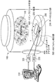
図1に、半導体製造工程に用いられるプラズマ処理装置100の概略を示す。この図において、プラズマ処理装置100で、プラズマ110を用いて、レジスト132でマスクした基板130を加工処理しているところを示している。プラズマ110は、真空(1Torr〜10−4Torr)中に、ガス(Cl2等)を導入し、高周波電界(400kHz〜2.45MHz)を印加して、プラズマ110を発生させている。このプラズマ110を用いて、レジスト132でマスクした基板130に基板電源(400kHz〜13.56GHz)を印加することにより加工処理を行っている。このプラズマ処理装置では、プラズマの気相反応制御(電子エネルギー分布制御,ガス分子構造の最適化,滞在時間制御等)と基板の表面反応制御(基板温度制御,表面不純物制御,反応生成物制御,基板バイアス制御等)を行う必要がある。
このプラズマ処理装置の評価方法としては、代表的なラングミュアー・プローブ等の探針を用いる評価方法がある。この探針を用いる評価方法は、プラズマ内部の特性を計測するのみで、プラズマより被処理材料に入射する各種粒子の密度やエネルギーの測定は不可能である。
【0003】
プラズマ処理装置により加工または堆積される被処理材料基板のパターン寸法は、数100nmのオーダーにまで微細化が進んでいる。したがって、このような微細パターンの内部にプラズマから入射する各種粒子の特性を計測する必要性が高まっている。
処理対象の基板に入射する粒子の特性を計測するために、平板にピンホールを形成し、その背後に阻止電界型エネルギー分析器を設置して、入射する粒子の計測を行っている。このような従来の方法は、ピンホールのサイズが〜mm程度と、実際の加工寸法とはかけ離れた値となっており、精密な入射粒子の計測が不可能であった。また、エネルギー分析器の分析管内での粒子間の衝突によるエネルギーや荷電状態の変化を抑制するために、差動排気システムが必要になるなど、現実の稼働中のプラズマ処理装置での測定は、事実上不可能であった。
このように、従来のプラズマ計測システムは装置が大掛りであり(プローブ、質量分析器等)プラズマへの擾乱も大きい。このため、最も重要であるマイクロ・ナノスケールでエッチング反応の進むウェハ表面上でのプラズマ計測は、従来のプラズマ計測システムでは不可能である。加えて装置コストも高いことなどから実際の生産装置に適用することが困難であった。
さて、半導体製造工程の微細加工の代表例として、シリコン酸化膜のプラズマ・エッチングが挙げられる。シリコン酸化膜のエッチングに寄与するためには、数100eVのエネルギーを有するイオンが必要である。このイオンのエネルギー分布を阻止電界型エネルギー分析器で計測しようとする場合、阻止電界発生電極に高電圧を印加する必要がある。
【0004】
【発明が解決しようとする課題】
本発明の目的は、プラズマ処理装置で、加工対象である基板の位置におけるモニタが可能であるオンウエハ・モニタリング・システムの提供である。
【0005】
【課題を解決するための手段】
上記目的を達成するために、本発明は、プラズマ処理装置の動作をオンウエハで計測することができるオンウエハ・モニタリング・システムであって、シリコン基板上に設けた、1つ又は複数のセンサ部,電源部,及び、外部との信号を入出力する入出力部を備え、前記センサ部には、半導体デバイスに該当するSiO 2 層のパターン部分と、該パターン部分の下に位置する分析素子部分とを有し、該パターン部分と該分析素子部分を貫通する微細穴を有し、該分析素子部分にはプラズマのイオン及び電子をエネルギーにより分離するために、複数の電極とを有するとともに、該パターン部分の直下の複数の電極の一番上である電極は前記シリコン基板と同電位とし、前記電源部は、プラズマ電位より電力を取り出すか、又は、PLZT素子の起電力により電力を取り出すことを特徴とする。
前記センサ部の複数の電極はAl電極であり、それぞれのAl電極間はγ−Al2O3で絶縁してもよい。このAl電極の側面は、薄い酸化膜皮膜で覆ってもよい。
前記センサとして、センサ部底部にコレクタ電極を有し、該コレクタ電極におけるイオン電流を測定して、イオン・エネルギー分布を得るイオン・エネルギー・分析器を含むことができる。
前記センサとして、パターン内に入射する光を絶縁膜中に発生する光誘起電流で検出するフォトン検出器であり、このフォトン検出器は、前記絶縁膜上に金属薄膜を形成し、該金属薄膜を透過した光のなかで、該金属の仕事関数と前記絶縁膜の伝導帯底とのエネルギー差に相当するエネルギー以上の光を検出することもできる。
また、前記センサとして、フォトダイオードで光を検出するフォトン検出器を含むことができる。
前記センサとして、電子銃からの電子とラジカル又はイオンとの衝突による発光を検出することでラジカルやイオンを特定するイオン・ラジカル分析器を含むことができ、このイオン・ラジカル分析器は、発光検出のために分光器を有することができる。
前記センサとして、電子電流,電子エネルギー分布,イオン電流,電子温度,電子密度,又は、電荷蓄積量の少なくとも1つを検出するプローブを含むこともできる。
【0006】
【発明の実施の形態】
本発明の実施形態を、図面を参照して詳細に説明する。
本発明におけるオンウエハ・モニタリング・システムの基本構造を図2および図3に示す。
図2において、オンウエハ・モニタリング・システム200は、基板上にセンサ等を作成して、プラズマ処理装置100中の処理対象基板の位置に置かれていることを示している。オンウエハ・モニタリング・システム200は、図3に示すように、基板上に作成された各種センサと、光で外部とデータの入出力を行うデータ入出力部210と、これらに電源を供給している電源部250とを備えている。オンウエハのデータ入出力部210は、外部に設置されている光による入出力部である、レーザ・ダイオード(LD)320やフォト・ダイオード(PD)330と接続されており、外部からの指令を受信したり、モニタしたデータを外部に送信する。
図2や図3に示したオンウエハ・モニタリング・システム200では基板上に、センサとして、イオン・エネルギー・アナライザ400,VUVフォトン検出器500,ラジカル・イオン種発光分光装置600を備えた例である。これらのセンサの構成は後で詳しく説明する。
【0007】
図3に示すように、これらの測定系をSiウエハ上に集積することで、様々なプラズマプロセス装置での計測を、容易に行なうことができる。図3には、電圧駆動系、信号検出系をSiウエハ上に電気回路を形成することで構築した例を示したが、Siウエハ上に、受光素子、発光素子を設置することで、センサーの駆動や信号の検出を、光を用いて真空装置の外から制御することもできる。本発明の特徴は、微細なセンサを用いて、プラズマ・プロセスの計測をワイアレスで行なうことにある。基本的に、オンウエハ・モニタリング・システムのセンサー部はマイクロマシン技術、信号処理部分はLSI技術を用いて開発する。
ワンチップのサイズについては、例えば2cm×2cm程度である。ウエハ・サイズは、最終的に8インチおよび12インチである。また、TEG(test element group)的なものではなく、専用ウエハに作りこみ、ウエハ面内の分布も全て計測できるものとする。
この様にして、イオン・エネルギー・アナライザ、イオン・エネルギー・アナライザーをベースとしたプローブ、フォトン検出器、およびイオン種・ラジカル種発光分光器をロックイン・アンプ、フォト・ダイオード、メモリ回路、スイッチング回路、フィルター回路、入出力信号系のLSIと集積化し、さらに電源系も1チップに作りこむ。データの送受信は全て光インターコネクトで行い、完全なワイアレス・インライン・システムを構築することができる。
また、図2に示すように、このオンウエハ・モニタリング・システムを用いて、取得したデータをワイヤレスでコンピュータ310に送信することにより、リアルタイムでプラズマ処理のプロセスをシミュレーションできる。また、このシミュレーションによる予測を、プラズマ発生装置にフィードバックして、プロセス進行中にプロセスを制御することもできる。
【0008】
<入出力部>
信号のワイアレス送受信のためには、フォト・ダイオード(PD)による光インターコネクト技術を用いている。
図4に入出力部の構成例を示す。図4(a)は、フォト・ダイオード212及び214による受信部を示している。外部のレーザ・ダイオード(LD)からの光信号による指令は、フォト・ダイオード212により受信され、バックグランド光を受けているフォト・ダイオード214からの出力と作動アンプ216により差を取られる。その後、選択回路218により、各センサ等に指令として送られる。
このように、光信号により、外部とオンウエハ・モニタリング・システム200とをワイヤレスで通信することができる。
【0009】
<電源>
さて、各種センサに供給する電源250は、基板上に作成されており、プラズマ処理装置100のプラズマにより発生するポテンシャル(数十V〜数百V)を利用して、電圧可変回路と結びつけることで電圧を制御している。
図5に電源部250の構成例を示している。図5において、プラズマ110におけるプラズマ空間電位とグランドとの電位差を電極271〜273で受けている。この電位差を受けて、トランジスタ252〜254及びトランジスタ255〜257をデコーダで流れる電流を制御することで、所望の電圧V=nRIを得ている。なお、Rは抵抗262〜264の抵抗値,nは抵抗の個数である。
より高電圧が必要な場合には、PLZT(チタン酸ジルコン酸ランタン鉛)素子を用いる。この素子では3kV/cm程度の電圧の供給が可能である。この例を図6に示す。図6において、分極処理をしたPLZT(チタン酸ジルコン酸ランタン鉛)素子280に対して波長365nm以上の紫外光を照射すると、その照射光強度に対応した内部電流が流れ、電極282及び電極284の間に、電極間距離に応じて3.3kV/cmの電圧が生じる。使用する紫外光としてはプラズマからの紫外光や外部から照射した紫外光を用いる。これにより、高電圧の電源をオンウエハ・モニタリング・システム200内部に設置することができる。このように、オンウエハ・モニタリング・システム200に供給する電源には、図5に示すようにウエハ上に発生したポテンシャルを取り出すことや、図6に示すように紫外線照射によって高電圧を発生させることの可能なPLZT(チタン酸ジルコン酸ランタン鉛)素子を用いることができる。
【0010】
<オンウエハ・イオン・エネルギー・アナライザ>
まず、オンウエハ・モニタリング・システム200に搭載するセンサの例として、図7及び図8を用いて、イオン・エネルギー・アナライザの構成について説明する。図7(a)は上から見た平面図であり、図7(b)は図7(a)のA−A’を切断した断面図である。図7(b)の半導体デバイスに該当するパターン・サイズを有する部分(図ではSiO2421)と、分析素子部分の下層にあるコレクタ電極413は、例えば図7(a)に示すようなジグザグの線状に形成する構造としている。図8は、図7に示した電極等を用いた測定装置全体の構成を示している。
半導体デバイスに該当するパターン部分(SiO2421)と、分析素子部分とを別々に有するために、分析素子部分に所定の微細穴(例えば100nm)さえ形成しておけば、分析素子における穴径や深さは、数μmまでのオーダで自由に設計することが可能となる。表面のシースやプラズマに対する擾乱は、デバイ長よりも小さいパターン・サイズにすることで防ぐことができる。
イオン・エネルギー・アナライザは、高アスペクト・パターン内で電圧・電流特性を測定できることが必要である。そのため、図7に示すように、プラズマ処理対象であるSiO2層421のパターンの下に電圧を印加する電極を埋め込むこととなる。印加する電圧は、シリコン酸化膜エッチングまで想定すると、〜1kVと極めて高いため、絶縁膜材料には高耐圧が必要である。そのため、材料の選定が極めて重要である。現状ではアルミを陽極酸化したAl2O3を用いるとよい。
【0011】
側壁電極には、電子リターディング電圧印加用電極424、イオン・エネルギー分離電圧用電極426、2次電子除去電極428が配置されている。各電極には、図8に示すように、流入電子の阻止電圧V1462、イオン・エネルギー分離用電圧V2464、2次電子除去電圧V3466が印加される。また、一番上(SiO2層421の直下)の側壁電極422は、図8に示すように、Si層411と直結して同電位としている。これは、通常のプラズマ・エッチング処理では、SiO2層421の下はSi層411であり、それをこのセンサで模擬的に実現するために行っている。
各電極の電圧を適当に設定することで、エッチング・パターン(図7ではSiO2層421)に入射する、電子電流/エネルギー、イオン電流/エネルギーの計測が行なえる他、入射粒子の中から、電子・イオンといった荷電粒子を除去し、中性粒子・フォトンの取り出しが可能である。
【0012】
イオン・エネルギー・アナライザ等では、入射イオン・エネルギーを分離するために、数百V以上の高電圧をミクロ領域に印加しなければならず、絶縁膜には高耐圧であるAl2O3が用いられている。電圧を印加するアルミ電極表面は薄い酸化膜皮膜で覆われており、ポリマーなどの堆積物があっても影響を受けない構造になっている。
イオン・エネルギー・アナライザ400では、イオン・エネルギー分離用電圧V2464として、図8に示すように、直線的に増加する電圧と、周波数発生器452からの一定周波数の電圧とを合成した電圧を印加する。そして、コレクタ電極413に流れる微小なイオン電流を測定するため、プラズマからのノイズに関してはロックイン・アンプ454を用いてノイズを除去して、電圧・イオン電流特性を測定する。その値を微分することでイオン・エネルギー分布を算出している。
【0013】
個々の電極は絶縁材料で分離されており、本発明では、電界コンデンサのバリア皮膜として用いられている高耐圧のγ−Al2O3を電極間の絶縁材料として使用している。計測する荷電粒子のエネルギーに応じて、他の絶縁材料(SiO2やその他のセラミック材料)を用いても構わない。また、計測の種類や必要な測定精度によっては、阻止電界発生用の電極の数を減じても構わない。
実際のプラズマ・プロセス中では、上記構造上に堆積物が形成される場合があり、この堆積物による阻止電界の変動が問題になる。例えば、SiO2をエッチングする場合、C−F系ガスを用いて行うと、側壁電極にテフロン(登録商標)のような構造を有する有機物が堆積する場合がある。本発明では、側壁に露出する電極表面に十分容量の大きな皮膜(例えば、Al2O3)を形成しておくことで、堆積物が測定に与える影響を抑えている。
【0014】
表面のシースやプラズマに対する擾乱は、デバイ長よりも小さいパターン・サイズにし、また、センサー表面は基板と同電位にすることで殆ど抑制することができる。
ノイズに対してはロックイン・アンプを用い、ノイズを除去してイオン電流を測定する方法を用いている。上述のように、基板内にロックインアンプ回路を形成することも可能であるが、光インターコネクトを用いて信号を外部に送信して、外部にロックインアンプを設置しても良い。
上述のオンウエハ・イオン・エネルギー・アナライザ400は、SiO2層のパターン内にあけた微細穴構造に入射するイオン・エネルギー分布を、プラズマからのノイズや堆積膜の影響無しに計測することができる。
【0015】
このイオン・エネルギー・アナライザの構造は、半導体デバイス製造技術を応用して、Siウエハ上に形成される。図9,図10は、製造過程の1例である。
図9(a)(1)において、シリコン基板411を酸化して、基板上に酸化膜412を形成し、アルミニウムを成膜した後、例えば図7(a)に示すように、ジグザグの線状にパターニングして、アルミニウム電極(コレクタ電極413)を形成する。次に、陽極酸化してアルミニウム層上にγ−Al2O3層を形成すると共に、形成したAl2O3層に対して、RIE(reactive ion etching)を行い、微細穴を形成する(図9(a)(2)参照)。
図9(b)(1)〜(3)に示すように、SiO2層をコレクタ電極のAl層413上に保護のためにCVD(chemical vapor deposition)により形成して、形成したSiO2層をCMP(chemical mechanical polishuing)することで、γ−Al2O3層とそろえて平坦にする。その上にアルミニウムをスパッタして電極を形成する。次にその電極にRIEを行って微細穴を形成した後、陽極酸化して、γ−Al2O3層427を形成する。この陽極酸化を行うときに、アルミニウムの電極の側面に露出している部分にAl2O3層を形成している。
この後に、γ−Al2O3層上のアルミニウム電極のスパッタ、RIEによる微細穴形成、陽極酸化によるγ−Al2O3層形成を、複数回(図では2回)繰り返して、最後にアルミニウム電極のスパッタ、RIEによる微細穴形成を行ったものが図9(c)に示されている。
次に、図10(d)(1)に示すように、先ほどCVDにより形成した保護のためのSiO2層をRIEにより取り除き、その後、微細穴内を含めて多結晶シリコンを形成する。そして、多結晶Siをエッチバックして平坦化する(図10(d)(2)参照)。そして、図10(e)に示すように、平坦化した平面上にSiO2層を形成し、形成したSiO2層に微細穴をRIEにより作成する。最終的に、多結晶シリコンをRIEにより取り除き、微細穴をコレクタ電極413まで貫通させる(図10(f)参照)。
このようにして、イオン・エネルギー・アナライザを、半導体デバイス製造技術を応用して、Siウエハ上に形成することができる。
【0016】
<オンウエハ・フォトン検出器>
オンウエハ・フォトン検出器は、パターン内に入射する真空紫外光(VUV)などの光の強度や波長などを、シリコン酸化膜,シリコン窒化膜,シリコン酸窒化膜などの絶縁膜中に発生する光誘起電流に変換して測定する。それぞれの材料のエネルギー・バンドギャップを越えるエネルギーを持つ光を検出するここができる。例えば、シリコン酸化膜は8.8eVであり、真空紫外光を計測することができる。シリコン窒化膜は5eVであり、シリコン酸窒化膜は前2つの値の間の値である。
また、絶縁膜上に1μm程度の金属薄膜を置くと、その金属内の電子密度で決まるプラズマ振動数を超える光のみ透過する。さらに、この金属膜を極薄膜化することで、プラズマ振動数以下の波長も透過する。このとき、金属の仕事関数と絶縁膜の伝導帯底とのエネルギー差に相当する光が、金属膜と絶縁膜との界面で吸収され、絶縁膜伝導帯に電子キャリヤを生成する、即ち光誘起電流が発生する。これにより、特定の波長の光を検出することができる。金属の種類・膜厚を変えることで、固有のプラズマ振動数あるいは仕事関数を変化させることができる。絶縁膜の種類・膜厚を変えることで固有のバンドギャップを変化させることができる。これにより、絶縁膜材料,金属,半導体(Si)を組み合わせることで、様々な波長の光を検出することができる。さらに、放射光だけパターン内に入射できるように電子やイオンをリターディングする電圧を印加して測定することもできるし、金属膜を絶縁膜上に堆積することによっても、電子やイオンを除去することができる。
フォトン検出器500の構成を図11(a)に示す。その構造は、図7に示したイオン・エネルギー・アナライザ400と基本的に同じであるが、図11(a)に示すように、底部の電極513の表面にSiO2膜514がカバーされている。前述のように、このシリコン酸化膜514は、シリコン窒化膜,シリコン酸窒化膜等の絶縁膜でもよく、絶縁膜の種類や厚さにより検出する光の波長を特定することができる。この絶縁膜514は、光の波長に対する吸光度が既知であり、膜厚を制御して設置している。この絶縁膜514中に発生する光誘起電流を、コレクタ電極513で集めて測定することでフォトンを測定する。コレクタ電極513に流れる電流をモニターすることで、パターン内に入射する光の波長に関する情報を得ることができる。
また、図11(b)に示すように、コレクタ電極の代わりに、Si基板561に45°の角度で加工した鏡563を形成し、入射した光のみを反射させ、フォトダイオード550で入射光強度を計測する構成としてもよい。
図11(a)及び(b)のフォトン検出器500においても、それぞれの電極には、図8に示したイオン・エネルギー・アナライザと同様の電圧を印加して、電子やイオンをコレクタ電極等には届かないようにしている。また、作成方法も図9及び図10と同様である。
【0017】
<オンウエハ・ラジカル・イオン種発光分光装置>
オンウエハ・ラジカル・イオン種発光分光装置は、基板に入射してくるイオンおよびラジカル種を特定するために、質量分析器の代わりに使用されるものである。質量分析器は質量を分離するのにある程度の距離が必要となり、シリコン基板上に作りこむことが難しい。また、長い距離輸送することで損失したり種々の反応が生じる可能性があり精度の良い測定が難しい。そこで、ミクロな領域でのイオン種、ラジカル種の特定が実現でき、微細化・集積化に対応できるマイクロ電子銃を用いた発光分光器を開発した。
図12に示すオンウエハ・ラジカル・イオン種発光分光装置600は、パターン644内に入射してくるイオン、電子、ラジカルを上述したイオン・エネルギー・アナライザで用いたものと同様の電極構造(638〜644)を用いて分離する。これらの電極には、電子を阻止する電圧622やイオンを阻止する電圧624を印加する。なお、ここで用いている電極構造はシリコンと窒化シリコンで構成しているが、図7と同様にAlとAl2O3を用いてもよい。
入射ラジカルおよびイオンは、マイクロ電子銃610により生成されるエネルギー可変電子ビームにより発光し、その発光をマイクロ分光器に伝搬して分光する。発光を分光器に伝搬させるために光導波路645を用いる。分光器は20nm以下の分解能で分光を行える。
また、同時にラジカルの電子ビームによるイオン化電位をイオン・コレクタ電極615により測定し、発光分光と併せてラジカルなどの特定を行える構造となっている。これは、電源614の電圧を変化させ、イオン・コレクタ電極615への印加電圧を変化させて電圧−電流特性を測定し、中性粒子固有の出現電位を求めることで、ラジカル放出を検出することができる。
【0018】
イオン種、ラジカル種を検出する発光分光器では、イオンやラジカルを発光させるための電子ビーム源をマイクロ電界放出型電子銃を用いて製作する。これを図13,図14を用いて説明する。
図13は、論文(JJAP 36(1997)L939)に記されている電界放出型電子銃である。この電子銃は、シリコン基板651上の酸化膜652にアルミの電極を設けている。この上にシリコン層654とシリコン酸化膜655を設けてプラチナの電極656を生成している。また、プラチナ電極656の1cm上に、電子を放出するための電界を印加するための電極657を設けている。アルミ電極653とプラチナ電極656間に電圧110V,プラチナ電極656とその上の電極657との間に電圧5kVを印加すると、放出電子密度1.4mA/cm2が得られている。
さて、電界放出電子電流に関するFowler-Nordheimの式は、仕事関数φ[eV]及び電界強度F[Vcm−1]に依存しており、電流密度J0に対して以下のことが成り立つ。
【数1】

【0019】
これを実現したものが図14に示した電子銃である。図14(a)は斜視図、図14(b)は上から見た平面図である。図13と同様の構成で、アルミニウム電極632,シリコン層633,SiO2層634,プラチナ電極635と、プラチナ電極636とで電子銃を構成している。電極615のカバー616やデポ避け用カバー637はSi3N4で作成されており、電極615やプラチナ電極635に堆積物が着くことを阻止している。
電子銃による発光は、SiON膜をSiO2膜で挟んだ構造のものか、SiO2表面にMgをドーピングした構造の導波路645により伝搬され、マイクロ分光器650で分光解析される。
【0020】
マイクロ分光器650の構成を図15で説明する。図15に示すように、入力光を、光導波路に設けた例えばのこぎり歯状に加工したブレーズド格子690で反射することで、波長λ1〜λ3にスペクトル分解して、受光素子674〜678で検出している。このように回折素子を半導体素子で作成することで、マイクロ分光器650を構成している。光導波路は、(a)に示すように屈折率が低い(n2)層の中に高い(n1)層を形成するか、(b)に示すように屈折率が低い(n2)層で高い(n1)層を挟むように形成する。この屈折率の違う層を作成するには、SiO2層にイオンドープにより屈折率が低い部分を作成するか、ポリイミドで導波路を形成してもよい。
マイクロ分光器を用いることで、微小な光でも感度良く検出される。ラジカルの場合には、同時にイオン化された電流値を観察することで、出現電位をモニタリングする。これら個別マイクロ・センサ技術を集積化する。
【0021】
オンウエハ・ラジカル・イオン種発光分光装置600の製造過程の1例を図16及び図17を用いて説明する。
図16(a)では、シリコン基板630上に酸化膜631を形成している。その酸化膜631上にシリコンを堆積してエッチングすることで、Si層633を形成する(図16(b)参照)。このSi層633にアルミニウムを蒸着することで電極632を形成する(図16(c)参照)。また、Si層633上にSiO2を堆積してエッチングすることでSiO2層634を形成する(図16(d)参照)。
次に、図16(e)に示すように、プラチナを堆積してパターニングすることで、電極635と電極636を形成する。そして、Si3N4を堆積してエッチングすることで、電極に対して保護を行うカバー637,616を形成する(図16(f)参照)。
図17(g),(h)に示すように、SiO2(犠牲層を含む)を堆積してエッチングするとともに、形成したSiO2上にSi3N4を堆積してエッチングすることで、電極615に対するカバー616を完成する。次に、導波路645を作成するために、SiO2を堆積してエッチングするとともに、イオンドープを行う(図17(i)参照)。
図17(j),(k)に示すように、プラズマからの電子やイオンを阻止するための電極を形成するために、Si3N4を堆積してエッチングした後に、この電極形成時に使用したSiO2の犠牲層もエッチングして取り除く。なお、図17(j),(k)のときに、図示していないが、パターン層として、例えば図12のSiO2層644や電極Si643も形成する。
【0022】
電子銃の他の構成を図18に示す。図14には、4角形で3辺から電子放出し、1辺に導波路645を設置する構成が記載されているが、図18に示すように、形状を円形としてもよい。図18において、同心円の電子放出用電極712とメッシュ電極714間に電圧を印加することで、電子銃から放出される電子を特定領域(同心円の中心部分)716に集中させることができる。
また、図19は、イオン・ラジカル分析器で、電子銃による発光を観測するための分析器として、光干渉多層膜と光ダイオードとを組み合わせた構成を使用するイオン・ラジカル分析器の概略を示す。図示の概略構成は、中性粒子等の電子衝突による発光を、光干渉多層膜で構成した狭帯域透過光学フィルタ844と光ダイオード843で検出している。このイオン・ラジカル分析器の構成の電子銃810としては、図18に示した電子銃の構成を用いることが適している。なお、光ダイオード842は、光干渉多層薄膜844を透過する紫外線等の光を検出しているフォトン検出器を構成している。
【0023】
<オンウエハ・プローブ>
オンウエハ・プローブは、図20に示すように、基本的に図7に示されているイオン・エネルギー・アナライザと同じ構造で、底部電極であるコレクターで電圧電流測定を行う。エッチング・パターン内に入ってくる電子電流、電子エネルギー分布,イオン電流、電子温度、電子密度、電荷蓄積量などの測定を、各電極に印加する電圧等を制御することで行うことのできるマイクロ・プローブである。これをオンウエハ・モニタリング・システムのセンサとして搭載することもできる。
【0024】
<その他の応用>
図7や図20に示したセンサ構造をプラズマにさらした後、各電極間に一定電圧を印加し、電極間を流れる電流を測定することで、側壁導電性のアスペクト依存性を容易に測定することができる。
また、各電極をそれぞれ、フラッシュ・メモリの制御電極に接続しておき、プラズマにさらした後、浮遊電極に蓄積された電荷を、制御電極のVthシフトとして測定することで、プラズマ・プロセスによる帯電量の深さ依存性を、一度に評価可能となる。
【0025】
<デポの影響>
本発明におけるプラズマ・オンウエハ・モニタリングは、主にプラズマ・エッチング・プロセスを想定している。特にシリコン酸化膜エッチングにおけるポリマー堆積などによりモニタリングに影響を及ぼすことが考えられる。そこで、本発明では、ポリマー堆積膜の影響を最小限に抑える工夫を行っている。イオン・エネルギー・アナライザにおいては側壁に電圧を印加して電子のリターディングやイオンのエネルギー分離を行うので側壁へのポリマー堆積は影響を与える。そこで、側壁電極表面を薄い絶縁膜で覆うことで、ポリマーなどの堆積があっても側壁の容量が殆ど変化しない状況を作ることができ、電圧変動などを抑制することができる。
また、コンタクト・ホール底部のイオン・コレクタ電極部分には高エネルギー・イオンが常に衝撃するのでポリマーの堆積は極めて少ないと言えるが、信頼性を高め、繰り返し使用回数を長くするためには、測定終了後に底部に高電圧を印加してArイオンあるいは酸素イオンにて表面をクリーニングできるようなシーケンスを組む必要がある。これはプローブやフォトン検出器についても同様の方法で堆積膜の影響を抑制することができる。一方、イオン種・ラジカル種発光分光分析装置に関して、入射イオン・レンズ系はイオン・エネルギー・アナライザと同様の工夫により堆積膜などの影響を制御することは可能である。
マイクロ電子銃および光導波路、マイクロ分光器については、電子銃をカバーする窒化膜スリットを設置したりレイアウトを工夫して、ラジカルが届かないようにする工夫をしている。
【0026】
<素子によるイオン・シースの擾乱、素子温度の上昇、電磁ノイズ対策>
素子によるイオン・シースの擾乱については、基板表面の電極とシリコン基板を同電位にすることで防ぐことができる。また、素子温度の上昇に関しては、全てのセンサーをシリコン基板内部にμmオーダー・サイズで作りこむため、エッチング装置の基板冷却により十分に制御することが可能である。電磁ノイズについては、ロックイン・アンプの回路をシリコン基板中に作りこみ、ノイズを除去してイオン電流を測定することで解決できる。
【0027】
【発明の効果】
上述するように、本発明のオンウエハ・モニタリング・システムは、プラズマ処理装置を計測するもので、プラズマ処理装置には何も改造を加えることなく、加工対象である基板の位置におけるモニタがオンラインで可能である。
【図面の簡単な説明】
【図1】プラズマ処理装置の概要を示す図である。
【図2】本発明のオンウエハ・モニタリング・システムの概略構成を示す図である。
【図3】オンウエハ・モニタリング・システムのウエハ上の構成例を示す図である。
【図4】オンウエハ・モニタリング・システムの入出力部の構成を示す図である。
【図5】オンウエハ・モニタリング・システムの電源の構成を示す図である。
【図6】電源の別の構成を示す図である。
【図7】オンウエハ・イオン・エネルギー・アナライザの構造を示す図である。
【図8】イオン・エネルギー・アナライザの測定系を示す図である。
【図9】イオン・エネルギー・アナライザの製造工程を示す図である。
【図10】イオン・エネルギー・アナライザの製造工程の続きを示す図である。
【図11】フォトン検出器の構成を示す図である。
【図12】イオン・ラジカル分析器の構成を示す図である。
【図13】電子銃の基本構成を示す図である。
【図14】イオン・ラジカル分析器に使用する電子銃の構成を示す図である。
【図15】マイクロ分光器の構成を示す図である。
【図16】イオン・ラジカル分析器の製造工程を示す図である。
【図17】イオン・ラジカル分析器の製造工程の続きを示す図である。
【図18】電子銃の他の構成を示す図である。
【図19】イオン・ラジカル分析器の他の概略構成を示す図である。
【図20】マイクロ・プローブの構成を示す図である。
【符号の説明】
100 プラズマ処理装置
110 プラズマ
130 シリコン基板
132 レジスト
200 オンウエハ・モニタリング・システム
210 データ入出力部
212,214 フォト・ダイオード
216 作動アンプ
218 選択回路
250 電源部
252,253,254,255,256,257 トランジスタ
262,263,264 抵抗
271,272,274 電極
280 PLZT素子
282,284 電極
400 イオン・エネルギー・アナライザ
411 シリコン基板
412 酸化膜
413 コレクタ電極
421 SiO2層
422 側壁電極
424 電子リターディング電圧印加用電極
426 イオン・エネルギー分離電圧用電極
427 絶縁層
428 2次電子除去電極
452 周波数発生器
454 ロックイン・アンプ
500 フォトン検出器
513 コレクタ電極
514 SiO2膜
550 フォトダイオード
561 シリコン基板
563 鏡
600 ラジカル・イオン種発光分光装置
610 マイクロ電子銃
614 電源
615 イオン・コレクタ電極
616 カバー
622 電子減速用電圧
624 イオン減速用電圧
630 シリコン基板
631 酸化膜
632 アルミニウム電極
633 シリコン層
634, SiO2層
635,636 プラチナ電極
637 デポ避け用カバー
644 パターン
645 光導波路
650 マイクロ分光器
651 シリコン基板
652 酸化膜
653 アルミ電極
654 シリコン層
655 シリコン酸化膜
656 プラチナ電極
657 電極
674 受光素子
690 ブレーズド格子
712 電子放出用電極
714 メッシュ電極
810 電子銃
842,843 光ダイオード
844 狭帯域透過光学フィルタ
637,616 カバー[0001]
BACKGROUND OF THE INVENTION
The present invention relates to a micro / nano sensing system technology for measuring plasma on a wafer surface in a plasma processing apparatus.
[0002]
[Technical background]
FIG. 1 shows an outline of a
As an evaluation method of this plasma processing apparatus, there is an evaluation method using a probe such as a typical Langmuir probe. This evaluation method using the probe only measures the internal characteristics of the plasma and cannot measure the density and energy of various particles incident on the material to be processed from the plasma.
[0003]
The pattern dimension of a substrate to be processed processed or deposited by a plasma processing apparatus has been miniaturized to the order of several hundred nm. Therefore, there is an increasing need to measure the characteristics of various particles incident from plasma into such a fine pattern.
In order to measure the characteristics of particles incident on a substrate to be processed, a pinhole is formed on a flat plate, and a blocking electric field energy analyzer is installed behind the pinhole to measure the incident particles. In such a conventional method, the pinhole size is about ~ mm, which is a value far from the actual processing dimension, and precise measurement of incident particles was impossible. Also, in order to suppress changes in energy and charge state due to collisions between particles in the analysis tube of the energy analyzer, a differential exhaust system is required, etc. It was virtually impossible.
As described above, the conventional plasma measurement system has a large apparatus (probe, mass analyzer, etc.) and has a large disturbance to the plasma. Therefore, the most important plasma measurement on the wafer surface where the etching reaction proceeds on the micro / nano scale is impossible with the conventional plasma measurement system. In addition, since the apparatus cost is high, it has been difficult to apply to an actual production apparatus.
A typical example of fine processing in a semiconductor manufacturing process is plasma etching of a silicon oxide film. In order to contribute to the etching of the silicon oxide film, ions having an energy of several hundred eV are required. In order to measure the energy distribution of ions with a blocking electric field type energy analyzer, it is necessary to apply a high voltage to the blocking electric field generating electrode.
[0004]
[Problems to be solved by the invention]
An object of the present invention is to provide an on-wafer monitoring system capable of monitoring the position of a substrate to be processed by a plasma processing apparatus.
[0005]
[Means for Solving the Problems]
In order to achieve the above object, the present invention provides an on-wafer monitoring system capable of measuring the operation of a plasma processing apparatus on-wafer, comprising one or more sensor units and a power source provided on a silicon substrate. And an input / output unit for inputting / outputting a signal to / from the outside,SiO applicable to semiconductor devices 2 LayeredPattern part andAn analysis element portion located below the pattern portion, and a fine hole penetrating the pattern portion and the analysis element portion.To separate plasma ions and electrons by energyIn addition,And having a plurality of electrodes,TheDirectly below the patternThe electrode that is the top of the plurality of electrodes isSame potential as the silicon substrateThe power supply unit takes out power from the plasma potential or takes out power from the electromotive force of the PLZT element.It is characterized by that.
The plurality of electrodes of the sensor unit are Al electrodes, and between each Al electrode is γ-Al2O3May be insulated. The side surface of the Al electrode may be covered with a thin oxide film.
The sensor may include an ion energy analyzer having a collector electrode at the bottom of the sensor unit and measuring an ion current at the collector electrode to obtain an ion energy distribution.
The sensor is a photon detector that detects light incident in a pattern by a photo-induced current generated in an insulating film. The photon detector forms a metal thin film on the insulating film, and the metal thin film is Of the transmitted light, it is possible to detect light having an energy equal to or higher than the energy difference between the work function of the metal and the conduction band bottom of the insulating film.
The sensor may include a photon detector that detects light with a photodiode.
The sensor can include an ion / radical analyzer that identifies radicals and ions by detecting light emission from collisions between electrons and radicals or ions from an electron gun. You can have a spectrograph for.
The sensor may include a probe that detects at least one of electron current, electron energy distribution, ion current, electron temperature, electron density, or charge accumulation amount.
[0006]
DETAILED DESCRIPTION OF THE INVENTION
Embodiments of the present invention will be described in detail with reference to the drawings.
2 and 3 show the basic structure of the on-wafer monitoring system in the present invention.
In FIG. 2, the on-
The on-
[0007]
As shown in FIG. 3, by integrating these measurement systems on the Si wafer, measurement with various plasma process apparatuses can be easily performed. FIG. 3 shows an example in which a voltage drive system and a signal detection system are constructed by forming an electric circuit on a Si wafer. However, by installing a light receiving element and a light emitting element on the Si wafer, Driving and signal detection can also be controlled from outside the vacuum apparatus using light. A feature of the present invention is that measurement of a plasma process is performed wirelessly using a fine sensor. Basically, the sensor part of the on-wafer monitoring system is developed using micromachine technology and the signal processing part using LSI technology.
The size of one chip is, for example, about 2 cm × 2 cm. The wafer size is finally 8 inches and 12 inches. In addition, it is not a TEG (test element group) type, but it is built on a dedicated wafer and all distributions within the wafer surface can be measured.
In this way, an ion energy analyzer, a probe based on an ion energy analyzer, a photon detector, and an ion species / radical species emission spectrometer are locked in an amplifier, a photo diode, a memory circuit, and a switching circuit. It is integrated with the filter circuit and input / output signal system LSI, and the power supply system is built on a single chip. Data transmission and reception are all performed via an optical interconnect, and a complete wireless inline system can be constructed.
Further, as shown in FIG. 2, by using this on-wafer monitoring system, the acquired data is transmitted to the
[0008]
<Input / output unit>
For the wireless transmission and reception of signals, an optical interconnect technology using a photodiode (PD) is used.
FIG. 4 shows a configuration example of the input / output unit. FIG. 4 (a) shows a receiving unit using the
In this way, the outside and the on-
[0009]
<Power supply>
Now, the
FIG. 5 shows a configuration example of the
When a higher voltage is required, a PLZT (lead lanthanum zirconate titanate) element is used. This element can supply a voltage of about 3 kV / cm. An example of this is shown in FIG. In FIG. 6, when a polarized PLZT (lead lanthanum zirconate titanate)
[0010]
<On-wafer ion energy analyzer>
First, as an example of a sensor mounted on the on-
Pattern parts applicable to semiconductor devices (SiO2421) and the analysis element part separately, so long as a predetermined fine hole (for example, 100 nm) is formed in the analysis element part, the hole diameter and depth in the analysis element are on the order of several μm. It becomes possible to design freely. Disturbances to the surface sheath and plasma can be prevented by making the pattern size smaller than the Debye length.
An ion energy analyzer must be able to measure voltage and current characteristics within a high aspect pattern. Therefore, as shown in FIG.2An electrode for applying a voltage is buried under the pattern of the
[0011]
An electron retarding
By appropriately setting the voltage of each electrode, an etching pattern (in FIG.2Electron current / energy and ion current / energy incident on the layer 421) can be measured, and charged particles such as electrons and ions can be removed from the incident particles, and neutral particles and photons can be taken out. .
[0012]
In an ion energy analyzer or the like, in order to separate incident ion energy, a high voltage of several hundred volts or more must be applied to the micro region, and the insulating film has a high withstand voltage Al.2O3Is used. The surface of the aluminum electrode to which the voltage is applied is covered with a thin oxide film, so that it is not affected by deposits such as polymers.
In the
[0013]
Each electrode is separated by an insulating material, and in the present invention, a high breakdown voltage γ-Al used as a barrier film of an electric capacitor.2O3Is used as an insulating material between the electrodes. Depending on the energy of the charged particles to be measured, other insulating materials (SiO2Or other ceramic materials) may be used. Further, depending on the type of measurement and the required measurement accuracy, the number of blocking electric field generating electrodes may be reduced.
In an actual plasma process, a deposit may be formed on the structure, and the fluctuation of the blocking electric field due to the deposit becomes a problem. For example, SiO2When etching is performed using a C—F-based gas, an organic substance having a structure such as Teflon (registered trademark) may be deposited on the sidewall electrode. In the present invention, a sufficiently large film (for example, Al2O3) To suppress the influence of the deposit on the measurement.
[0014]
Disturbances to the surface sheath and plasma can be almost suppressed by making the pattern size smaller than the Debye length and setting the sensor surface to the same potential as the substrate.
For noise, a lock-in amplifier is used to remove the noise and measure the ion current. As described above, a lock-in amplifier circuit can be formed in the substrate, but a signal may be transmitted to the outside using an optical interconnect, and the lock-in amplifier may be installed outside.
The on-wafer
[0015]
The structure of this ion energy analyzer is formed on a Si wafer by applying semiconductor device manufacturing technology. 9 and 10 show an example of the manufacturing process.
9A and 9A, the
As shown in FIGS. 9 (b) (1) to (3), SiO2A layer is formed on the
After this, γ-Al2O3On the layeraluminumElectrode sputtering, microhole formation by RIE, γ-Al by anodic oxidation2O3Repeat layer formation multiple times (twice in the figure) and finallyaluminumFIG. 9C shows a case where fine holes are formed by electrode sputtering and RIE.
Next, as shown in FIGS. 10 (d) and (1), the protective SiO film formed by CVD is protected.2The layer is removed by RIE, and then polycrystalline silicon is formed, including in the micro holes. Then, the polycrystalline Si is etched back and planarized (see FIGS. 10D and 10B). And FIG.e) On the planarized plane as shown in FIG.2Layer is formed, and the formed SiO2Microholes are created in the layer by RIE. Finally, the polycrystalline silicon is removed by RIE, and the fine hole is penetrated to the collector electrode 413 (see FIG. 10F).
In this way, the ion energy analyzer can be formed on the Si wafer by applying the semiconductor device manufacturing technology.
[0016]
<On-wafer photon detector>
An on-wafer photon detector is a light-induced device that generates the intensity and wavelength of light such as vacuum ultraviolet light (VUV) incident on a pattern in an insulating film such as a silicon oxide film, a silicon nitride film, or a silicon oxynitride film. Convert to current and measure. This is where you can detect light with energy exceeding the bandgap of each material. For example, the silicon oxide film is 8.8 eV, and vacuum ultraviolet light can be measured. The silicon nitride film is 5 eV, and the silicon oxynitride film has a value between the previous two values.
When a metal thin film of about 1 μm is placed on the insulating film, only light exceeding the plasma frequency determined by the electron density in the metal is transmitted. Furthermore, by making this metal film very thin, wavelengths below the plasma frequency are transmitted. At this time, light corresponding to the energy difference between the work function of the metal and the bottom of the conduction band of the insulating film is absorbed at the interface between the metal film and the insulating film, generating electron carriers in the insulating film conduction band, that is, photoinduced. A current is generated. Thereby, light of a specific wavelength can be detected. By changing the metal type and film thickness, the inherent plasma frequency or work function can be changed. The inherent band gap can be changed by changing the type and film thickness of the insulating film. Thereby, it is possible to detect light of various wavelengths by combining the insulating film material, metal, and semiconductor (Si). Furthermore, it is possible to measure by applying a voltage for retarding electrons and ions so that only the emitted light can enter the pattern, or by depositing a metal film on the insulating film, the electrons and ions can be removed. be able to.
The configuration of the
Further, as shown in FIG. 11B, instead of the collector electrode, a
Also in the
[0017]
<On-wafer, radical, and ion-type emission spectrometer>
The on-wafer radical ion species emission spectrometer is used in place of a mass spectrometer to identify ions and radical species incident on a substrate. A mass spectrometer requires a certain distance to separate masses, and is difficult to build on a silicon substrate. Moreover, there is a possibility of loss or various reactions due to long-distance transportation, and accurate measurement is difficult. Therefore, we have developed an emission spectrometer that uses a micro electron gun that can identify ionic species and radical species in the microscopic region and can be used for miniaturization and integration.
The on-wafer radical ion luminescence spectroscopic device 600 shown in FIG. 12 has the same electrode structure (638 to 644) as that used in the above-described ion energy analyzer for ions, electrons, and radicals incident on the pattern 644. ) To separate. A
Incident radicals and ions are emitted by an energy variable electron beam generated by the
At the same time, the ionization potential of the radical due to the electron beam is measured by the
[0018]
In an emission spectrometer that detects ion species and radical species, an electron beam source for emitting ions and radicals is manufactured using a micro field emission electron gun. This will be described with reference to FIGS.
FIG. 13 shows a field emission electron gun described in a paper (JJAP 36 (1997) L939). In this electron gun, an aluminum electrode is provided on an
Now, the Fowler-Nordheim equation for the field emission electron current is expressed by the work function φ [eV] and the electric field strength F [Vcm.-1Current density J0The following holds true.
[Expression 1]
[0019]
This is realized by the electron gun shown in FIG. FIG. 14A is a perspective view, and FIG. 14B is a plan view seen from above. The
Light emission by the electron gun is achieved by changing the SiON film to SiO2It has a structure sandwiched between films, or SiO2The light is propagated through a waveguide 645 having a structure doped with Mg on the surface, and is spectrally analyzed by the micro-spectrometer 650.
[0020]
The configuration of the micro-spectrometer 650 will be described with reference to FIG. As shown in FIG. 15, the input light is reflected by a blazed grating 690 processed into, for example, a sawtooth shape provided in an optical waveguide.1~ Λ3Is detected by the
By using a micro-spectrometer, even minute light can be detected with high sensitivity. In the case of radicals, the appearance potential is monitored by simultaneously observing the ionized current value. These individual micro sensor technologies will be integrated.
[0021]
An example of the manufacturing process of the on-wafer radical / ion species emission spectrometer 600 will be described with reference to FIGS.
In FIG. 16A, an
Next, as shown in FIG. 16E, platinum is deposited and patterned to form an
As shown in FIGS. 17 (g) and 17 (h), SiO2(Including sacrificial layer) is deposited and etched, and the formed SiO2Si on3N4The
As shown in FIGS. 17J and 17K, in order to form an electrode for blocking electrons and ions from plasma, Si3N4After depositing and etching, SiO used for forming this electrode was used.2The sacrificial layer is also etched away. Although not shown in FIGS. 17J and 17K, as the pattern layer, for example, SiO in FIG.2A layer 644 and an electrode Si643 are also formed.
[0022]
Another configuration of the electron gun is shown in FIG. FIG. 14 shows a configuration in which electrons are emitted from three sides in a quadrangular shape and a waveguide 645 is installed on one side, but the shape may be circular as shown in FIG. In FIG. 18, by applying a voltage between the concentric electron emission electrode 712 and the mesh electrode 714, electrons emitted from the electron gun can be concentrated on a specific region (a central portion of the concentric circle) 716.
FIG. 19 shows an outline of an ion / radical analyzer that uses a configuration in which an optical interference multilayer film and a photodiode are combined as an analyzer for observing light emission by an electron gun. . In the schematic configuration shown in the figure, light emission due to electron collisions such as neutral particles is detected by a narrow-band transmission optical filter 844 and a photodiode 843 that are formed of an optical interference multilayer film. As the electron gun 810 having this ion / radical analyzer configuration, it is suitable to use the configuration of the electron gun shown in FIG. Note that the photodiode 842 constitutes a photon detector that detects light such as ultraviolet rays transmitted through the optical interference multilayer thin film 844.
[0023]
<On-wafer probe>
As shown in FIG. 20, the on-wafer probe basically has the same structure as the ion energy analyzer shown in FIG. 7, and performs voltage / current measurement with a collector as a bottom electrode. Measurement of electron current, electron energy distribution, ion current, electron temperature, electron density, charge accumulation amount, etc. entering the etching pattern can be performed by controlling the voltage applied to each electrode. It is a probe. This can be mounted as a sensor of an on-wafer monitoring system.
[0024]
<Other applications>
After the sensor structure shown in FIGS. 7 and 20 is exposed to plasma, a constant voltage is applied between the electrodes, and the current flowing between the electrodes is measured to easily measure the side wall conductivity aspect dependency. be able to.
In addition, each electrode is connected to the control electrode of the flash memory, and after being exposed to plasma, the electric charge accumulated in the floating electrode is changed to V of the control electrode.thBy measuring as a shift, it becomes possible to evaluate the depth dependency of the charge amount by the plasma process at a time.
[0025]
<Influence of Depot>
The plasma-on-wafer monitoring in the present invention mainly assumes a plasma etching process. In particular, monitoring may be affected by polymer deposition in silicon oxide film etching. Therefore, in the present invention, a contrivance is made to minimize the influence of the polymer deposited film. In the ion energy analyzer, voltage is applied to the side wall to retard electrons and separate energy of ions, so that polymer deposition on the side wall has an effect. Thus, by covering the sidewall electrode surface with a thin insulating film, it is possible to create a situation in which the capacitance of the sidewall hardly changes even if polymer or the like is deposited, and voltage fluctuations can be suppressed.
In addition, the high energy ions always bombard the ion collector electrode at the bottom of the contact hole, so it can be said that polymer deposition is extremely small. However, in order to improve reliability and increase the number of repeated use, the measurement is completed. It is necessary to set up a sequence that can later apply a high voltage to the bottom and clean the surface with Ar ions or oxygen ions. This can also suppress the influence of the deposited film on the probe and photon detector in the same manner. On the other hand, regarding the ion species / radical species emission spectroscopic analyzer, the incident ion / lens system can control the influence of the deposited film and the like by the same device as the ion energy analyzer.
The micro-electron gun, optical waveguide, and micro-spectrometer are devised to prevent radicals from reaching by installing a nitride film slit or covering the electron gun.
[0026]
<Ion / sheath disturbance by element, rise in element temperature, electromagnetic noise countermeasure>
The disturbance of the ion sheath due to the element can be prevented by setting the electrode on the substrate surface and the silicon substrate to the same potential. Further, the rise in element temperature can be sufficiently controlled by cooling the substrate of the etching apparatus because all sensors are formed in the silicon substrate with a size of the order of μm. Electromagnetic noise can be solved by building a lock-in amplifier circuit in the silicon substrate, removing the noise, and measuring the ionic current.
[0027]
【The invention's effect】
As described above, the on-wafer monitoring system of the present invention measures a plasma processing apparatus, and it is possible to monitor the position of a substrate to be processed online without modifying the plasma processing apparatus. It is.
[Brief description of the drawings]
FIG. 1 is a diagram showing an outline of a plasma processing apparatus.
FIG. 2 is a diagram showing a schematic configuration of an on-wafer monitoring system of the present invention.
FIG. 3 is a diagram showing a configuration example on a wafer of an on-wafer monitoring system.
FIG. 4 is a diagram illustrating a configuration of an input / output unit of an on-wafer monitoring system.
FIG. 5 is a diagram showing a configuration of a power source of an on-wafer monitoring system.
FIG. 6 is a diagram showing another configuration of the power supply.
FIG. 7 is a diagram showing the structure of an on-wafer ion energy analyzer.
FIG. 8 is a diagram showing a measurement system of an ion energy analyzer.
FIG. 9 is a diagram showing a manufacturing process of an ion energy analyzer.
FIG. 10 is a diagram showing a continuation of the manufacturing process of the ion energy analyzer.
FIG. 11 is a diagram showing a configuration of a photon detector.
FIG. 12 is a diagram showing a configuration of an ion / radical analyzer.
FIG. 13 is a diagram showing a basic configuration of an electron gun.
FIG. 14 is a diagram showing a configuration of an electron gun used in an ion / radical analyzer.
FIG. 15 is a diagram showing a configuration of a micro-spectrometer.
FIG. 16 is a diagram showing a manufacturing process of the ion / radical analyzer.
FIG. 17 is a diagram showing a continuation of the manufacturing process of the ion / radical analyzer.
FIG. 18 is a diagram showing another configuration of the electron gun.
FIG. 19 is a diagram showing another schematic configuration of the ion / radical analyzer.
FIG. 20 is a diagram showing a configuration of a micro probe.
[Explanation of symbols]
100 Plasma processing equipment
110 Plasma
130 Silicon substrate
132 resist
200 On-wafer monitoring system
210 Data input / output section
212, 214 Photo diode
216 Operational amplifier
218 selection circuit
250 Power supply
252,253,254,255,256,257 transistor
262, 263, 264 resistance
271,272,274 electrode
280 PLZT element
282,284 electrodes
400 Ion Energy Analyzer
411 Silicon substrate
412 Oxide film
413 Collector electrode
421 SiO2layer
422 Side wall electrode
424 Electron retarding voltage application electrode
426 Electrode for ion energy separation voltage
427 Insulating layer
428 Secondary electron removal electrode
452 Frequency generator
454 Lock-in amplifier
500 Photon detector
513 Collector electrode
514 SiO2film
550 photodiode
561 Silicon substrate
563 mirror
600 Radiation / Ion Species Emission Spectrometer
610 Micro electron gun
614 Power supply
615 Ion collector electrode
616 cover
622 Voltage for electronic deceleration
624 Ion deceleration voltage
630 silicon substrate
631 Oxide film
632 Aluminum electrode
633 Silicon layer
634, SiO2layer
635,636 Platinum electrode
637 Depot avoidance cover
644 patterns
645 Optical waveguide
650 Micro-spectrometer
651 Silicon substrate
652 Oxide film
653 Aluminum electrode
654 Silicon layer
655 Silicon oxide film
656 Platinum electrode
657 electrode
674 Light receiving element
690 blazed lattice
712 Electron emission electrode
714 mesh electrode
810 electron gun
842, 843 Photodiode
844 Narrow band transmission optical filter
637,616 Cover
Claims (11)
シリコン基板上に設けた、1つ又は複数のセンサ部,電源部,及び、外部との信号を入出力する入出力部を備え、
前記センサ部には、半導体デバイスに該当するSiO 2 層のパターン部分と、該パターン部の下に位置する分析素子部分とを有し、該パターン部分と該分析素子部分を貫通する微細穴を有し、該分析素子部分にはプラズマのイオン及び電子をエネルギーにより分離するために、複数の電極とを有するとともに、該パターン部分の直下の複数の電極の一番上である電極は前記シリコン基板と同電位とし、
前記電源部は、プラズマ電位より電力を取り出すか、又は、PLZT素子の起電力により電力を取り出す
ことを特徴とするオンウエハ・モニタリング・システム。An on-wafer monitoring system capable of measuring the operation of a plasma processing apparatus on-wafer,
Provided with one or more sensor units, power supply units, and input / output units for inputting / outputting signals to / from the outside, provided on the silicon substrate
The sensor part has a pattern part of the SiO 2 layer corresponding to the semiconductor device and an analysis element part located under the pattern part, and has a fine hole penetrating the pattern part and the analysis element part. The analysis element portion includes a plurality of electrodes for separating plasma ions and electrons by energy, and the electrode at the top of the plurality of electrodes immediately below the pattern portion is connected to the silicon substrate. The same potential ,
The on-wafer monitoring system is characterized in that the power supply unit takes out electric power from a plasma potential or takes out electric power from an electromotive force of a PLZT element .
前記センサ部の複数の電極はAl電極であり、それぞれのAl電極間はγ−Al2O3で絶縁されている
ことを特徴とするオンウエハ・モニタリング・システム。The on-wafer monitoring system according to claim 1,
The plurality of electrodes of the sensor section are Al electrodes, and the Al electrodes are insulated by γ-Al 2 O 3. An on-wafer monitoring system, wherein:
前記Al電極の側面は、薄い酸化膜皮膜で覆うことを特徴とするオンウエハ・モニタリング・システム。The on-wafer monitoring system according to claim 2,
An on-wafer monitoring system, wherein a side surface of the Al electrode is covered with a thin oxide film.
前記入出力部は、光で外部との信号の入出力を行うことを特徴とするオンウエハ・モニタリング・システム。In the on-wafer monitoring system according to any one of claims 1 to 3 ,
The on-wafer monitoring system is characterized in that the input / output unit inputs / outputs signals from / to the outside using light.
前記センサとして、センサ部底部にコレクタ電極を有し、該コレクタ電極におけるイオン電流を測定して、イオン・エネルギー分布を得るイオン・エネルギー・分析器を含むことを特徴とするオンウエハ・モニタリング・システム。In the on-wafer monitoring system according to any one of claims 1 to 4 ,
An on-wafer monitoring system comprising: a collector electrode at the bottom of the sensor section as the sensor; and an ion energy analyzer that obtains an ion energy distribution by measuring an ion current at the collector electrode.
前記センサとして、パターン内に入射する光を絶縁膜中に発生する光誘起電流で検出するフォトン検出器を含むことを特徴とするオンウエハ・モニタリング・システム。In the on-wafer monitoring system according to any one of claims 1 to 5 ,
An on-wafer monitoring system comprising a photon detector for detecting light incident on a pattern by a photo-induced current generated in an insulating film as the sensor.
前記フォトン検出器は、前記絶縁膜上に金属薄膜を形成し、該金属薄膜を透過した光のなかで、該金属の仕事関数と前記絶縁膜の伝導帯底とのエネルギー差に相当するエネルギー以上の光を検出することを特徴とするオンウエハ・モニタリング・システム。The on-wafer monitoring system according to claim 6 ,
The photon detector has a metal thin film formed on the insulating film, and has an energy equal to or higher than an energy corresponding to an energy difference between a work function of the metal and a conduction band bottom of the insulating film in light transmitted through the metal thin film. On-wafer monitoring system characterized by detecting light from
前記センサとして、フォトダイオードで光を検出するフォトン検出器を含むことを特徴とするオンウエハ・モニタリング・システム。In the on-wafer monitoring system according to any one of claims 1 to 5 ,
An on-wafer monitoring system comprising a photon detector that detects light with a photodiode as the sensor.
前記センサとして、電子銃からの電子とラジカル又はイオンとの衝突による発光を検出することでラジカルやイオンを特定するイオン・ラジカル分析器を含むことを特徴とするオンウエハ・モニタリング・システム。In the on-wafer monitoring system according to any one of claims 1 to 8 ,
An on-wafer monitoring system comprising an ion / radical analyzer that identifies radicals and ions by detecting light emitted from an electron gun and a radical or ion colliding as the sensor.
前記イオン・ラジカル分析器は、発光検出のために分光器を有することを特徴とするオンウエハ・モニタリング・システム。The on-wafer monitoring system according to claim 9 ,
The on-wafer monitoring system, wherein the ion radical analyzer has a spectrometer for detecting luminescence.
前記センサとして、電子電流,電子エネルギー分布,イオン電流,電子温度,電子密度,又は、電荷蓄積量の少なくとも1つを検出するプローブを含むことを特徴とするオンウエハ・モニタリング・システム。In the on-wafer monitoring system according to any one of claims 1 to 10 ,
An on-wafer monitoring system comprising: a probe for detecting at least one of an electron current, an electron energy distribution, an ion current, an electron temperature, an electron density, and a charge accumulation amount as the sensor.
Priority Applications (5)
| Application Number | Priority Date | Filing Date | Title |
|---|---|---|---|
| JP2002086196A JP4175456B2 (en) | 2002-03-26 | 2002-03-26 | On-wafer monitoring system |
| CNB038047322A CN100375245C (en) | 2002-03-26 | 2003-02-03 | On Wafer Monitoring System |
| PCT/JP2003/001079 WO2003081654A1 (en) | 2002-03-26 | 2003-02-03 | On-wafer monitoring system |
| US10/501,351 US7520956B2 (en) | 2002-03-26 | 2003-02-03 | On-wafer monitoring system |
| TW092103302A TWI263277B (en) | 2002-03-26 | 2003-02-18 | On-wafer monitoring system |
Applications Claiming Priority (1)
| Application Number | Priority Date | Filing Date | Title |
|---|---|---|---|
| JP2002086196A JP4175456B2 (en) | 2002-03-26 | 2002-03-26 | On-wafer monitoring system |
Publications (2)
| Publication Number | Publication Date |
|---|---|
| JP2003282546A JP2003282546A (en) | 2003-10-03 |
| JP4175456B2 true JP4175456B2 (en) | 2008-11-05 |
Family
ID=28449292
Family Applications (1)
| Application Number | Title | Priority Date | Filing Date |
|---|---|---|---|
| JP2002086196A Expired - Fee Related JP4175456B2 (en) | 2002-03-26 | 2002-03-26 | On-wafer monitoring system |
Country Status (5)
| Country | Link |
|---|---|
| US (1) | US7520956B2 (en) |
| JP (1) | JP4175456B2 (en) |
| CN (1) | CN100375245C (en) |
| TW (1) | TWI263277B (en) |
| WO (1) | WO2003081654A1 (en) |
Families Citing this family (64)
| Publication number | Priority date | Publication date | Assignee | Title |
|---|---|---|---|---|
| US7960670B2 (en) | 2005-05-03 | 2011-06-14 | Kla-Tencor Corporation | Methods of and apparatuses for measuring electrical parameters of a plasma process |
| US6830650B2 (en) * | 2002-07-12 | 2004-12-14 | Advanced Energy Industries, Inc. | Wafer probe for measuring plasma and surface characteristics in plasma processing environments |
| JP3868427B2 (en) | 2004-02-23 | 2007-01-17 | 株式会社半導体理工学研究センター | Real-time monitoring device for plasma process |
| US20060043063A1 (en) * | 2004-09-02 | 2006-03-02 | Mahoney Leonard J | Electrically floating diagnostic plasma probe with ion property sensors |
| JP4650383B2 (en) * | 2006-09-12 | 2011-03-16 | 株式会社デンソー | UV detector |
| KR100978754B1 (en) * | 2008-04-03 | 2010-08-30 | 주식회사 테스 | Plasma processing equipment |
| KR100823302B1 (en) * | 2006-12-08 | 2008-04-17 | 주식회사 테스 | Plasma processing equipment |
| US20080277064A1 (en) * | 2006-12-08 | 2008-11-13 | Tes Co., Ltd. | Plasma processing apparatus |
| JP2008166660A (en) * | 2007-01-05 | 2008-07-17 | Matsushita Electric Ind Co Ltd | Semiconductor manufacturing equipment |
| JP5407019B2 (en) | 2007-08-31 | 2014-02-05 | ラピスセミコンダクタ株式会社 | Plasma monitoring method |
| JP2009059879A (en) | 2007-08-31 | 2009-03-19 | Oki Electric Ind Co Ltd | Ultraviolet light monitoring system |
| JP4914789B2 (en) | 2007-09-03 | 2012-04-11 | ラピスセミコンダクタ株式会社 | Plasma process detection sensor, method for manufacturing the sensor, and method for manufacturing a semiconductor device using the sensor |
| JP2009164425A (en) * | 2008-01-08 | 2009-07-23 | Oki Semiconductor Co Ltd | Real-time monitor device and operation method |
| US7777179B2 (en) * | 2008-03-31 | 2010-08-17 | Tokyo Electron Limited | Two-grid ion energy analyzer and methods of manufacturing and operating |
| US7875859B2 (en) * | 2008-03-31 | 2011-01-25 | Tokyo Electron Limited | Ion energy analyzer and methods of manufacturing and operating |
| JP5255907B2 (en) * | 2008-05-26 | 2013-08-07 | ラピスセミコンダクタ株式会社 | Plasma monitoring system |
| JP2010010171A (en) * | 2008-06-24 | 2010-01-14 | Hitachi High-Technologies Corp | Plasma treatment apparatus, method for acquiring plasma treatment condition and plasma treatment method |
| JP5271768B2 (en) | 2009-03-26 | 2013-08-21 | ラピスセミコンダクタ株式会社 | Plasma monitoring method |
| US11615941B2 (en) | 2009-05-01 | 2023-03-28 | Advanced Energy Industries, Inc. | System, method, and apparatus for controlling ion energy distribution in plasma processing systems |
| US9287092B2 (en) | 2009-05-01 | 2016-03-15 | Advanced Energy Industries, Inc. | Method and apparatus for controlling ion energy distribution |
| US9435029B2 (en) | 2010-08-29 | 2016-09-06 | Advanced Energy Industries, Inc. | Wafer chucking system for advanced plasma ion energy processing systems |
| US9287086B2 (en) | 2010-04-26 | 2016-03-15 | Advanced Energy Industries, Inc. | System, method and apparatus for controlling ion energy distribution |
| US9767988B2 (en) | 2010-08-29 | 2017-09-19 | Advanced Energy Industries, Inc. | Method of controlling the switched mode ion energy distribution system |
| US7993937B2 (en) * | 2009-09-23 | 2011-08-09 | Tokyo Electron Limited | DC and RF hybrid processing system |
| US8889021B2 (en) * | 2010-01-21 | 2014-11-18 | Kla-Tencor Corporation | Process condition sensing device and method for plasma chamber |
| KR101656762B1 (en) | 2010-03-16 | 2016-09-12 | 가부시키가이샤 토호쿠 테크노 아치 | System, method, and a medium in which program is stored for predicting processing shape by plasma processing |
| US9309594B2 (en) | 2010-04-26 | 2016-04-12 | Advanced Energy Industries, Inc. | System, method and apparatus for controlling ion energy distribution of a projected plasma |
| FR2961009A1 (en) * | 2010-06-03 | 2011-12-09 | Ion Beam Services | SECONDARY ELECTRON ELECTRON DETECTOR |
| US9362089B2 (en) | 2010-08-29 | 2016-06-07 | Advanced Energy Industries, Inc. | Method of controlling the switched mode ion energy distribution system |
| JP5709505B2 (en) * | 2010-12-15 | 2015-04-30 | 東京エレクトロン株式会社 | Plasma processing apparatus, plasma processing method, and storage medium |
| US9366601B1 (en) * | 2011-03-15 | 2016-06-14 | University Of North Texas | Wafer fabrication monitoring/control system and method |
| CN103534780B (en) | 2011-03-28 | 2016-07-06 | 东京毅力科创株式会社 | Ion energy analysis instrument, in this ion energy analysis instrument the method for the method of electrical signal and manufacture and this ion energy analysis instrument of operation |
| JP2012243844A (en) * | 2011-05-17 | 2012-12-10 | Advantest Corp | Power supply apparatus and measuring device |
| US9210790B2 (en) * | 2012-08-28 | 2015-12-08 | Advanced Energy Industries, Inc. | Systems and methods for calibrating a switched mode ion energy distribution system |
| US9685297B2 (en) | 2012-08-28 | 2017-06-20 | Advanced Energy Industries, Inc. | Systems and methods for monitoring faults, anomalies, and other characteristics of a switched mode ion energy distribution system |
| WO2014036000A1 (en) * | 2012-08-28 | 2014-03-06 | Advanced Energy Industries, Inc. | Wide dynamic range ion energy bias control; fast ion energy switching; ion energy control and a pulsed bias supply; and a virtual front panel |
| KR101334384B1 (en) | 2012-08-31 | 2013-11-29 | 한국생산기술연구원 | Gas analysis apparatus in process chamber |
| JP2014029860A (en) * | 2013-08-27 | 2014-02-13 | Advantest Corp | Power supply device and measuring device |
| JP5837012B2 (en) * | 2013-09-12 | 2015-12-24 | ラピスセミコンダクタ株式会社 | MONITORING METHOD, PLASMA MONITORING METHOD, MONITORING SYSTEM, AND PLASMA MONITORING SYSTEM |
| JP2017188236A (en) * | 2016-04-03 | 2017-10-12 | 国立大学法人東北大学 | Measurement method for plasma state in plasma processing apparatus, and plasma measurement device used for the measurement method |
| TWI715599B (en) * | 2016-07-12 | 2021-01-11 | 台灣超微光學股份有限公司 | Spectrometer and manufacturing method thereof |
| US10957807B2 (en) * | 2017-04-19 | 2021-03-23 | The Board Of Trustees Of The University Of Alabama | PLZT thin film capacitors apparatus with enhanced photocurrent and power conversion efficiency and method thereof |
| TWI804836B (en) | 2017-11-17 | 2023-06-11 | 新加坡商Aes 全球公司 | Method and system for plasma processing and relevant non-transitory computer-readable medium |
| US12505986B2 (en) | 2017-11-17 | 2025-12-23 | Advanced Energy Industries, Inc. | Synchronization of plasma processing components |
| WO2019099925A1 (en) | 2017-11-17 | 2019-05-23 | Advanced Energy Industries, Inc. | Spatial and temporal control of ion bias voltage for plasma processing |
| US12230476B2 (en) | 2017-11-17 | 2025-02-18 | Advanced Energy Industries, Inc. | Integrated control of a plasma processing system |
| CN111788654B (en) | 2017-11-17 | 2023-04-14 | 先进工程解决方案全球控股私人有限公司 | Improved Application of Modulated Power Supply in Plasma Processing System |
| US11437221B2 (en) | 2017-11-17 | 2022-09-06 | Advanced Energy Industries, Inc. | Spatial monitoring and control of plasma processing environments |
| CN108461412A (en) * | 2018-03-22 | 2018-08-28 | 北京北方华创微电子装备有限公司 | On-line monitoring system and semiconductor processing equipment |
| CN114222958B (en) | 2019-07-12 | 2024-03-19 | 先进工程解决方案全球控股私人有限公司 | Bias power supply with single controlled switch |
| US12449309B2 (en) * | 2019-08-06 | 2025-10-21 | Applied Materials, Inc. | Methods for detection using optical emission spectroscopy |
| US11293993B2 (en) * | 2019-09-04 | 2022-04-05 | Applied Materials Israel Ltd. | Detection of an electric arc hazard related to a wafer |
| WO2021089127A1 (en) * | 2019-11-05 | 2021-05-14 | Ev Group E. Thallner Gmbh | Method for producing an analytical device |
| US12125674B2 (en) | 2020-05-11 | 2024-10-22 | Advanced Energy Industries, Inc. | Surface charge and power feedback and control using a switch mode bias system |
| EP3968353A1 (en) | 2020-09-10 | 2022-03-16 | Impedans Ltd | Apparatus for ion energy analysis of plasma processes |
| CN111948700B (en) * | 2020-09-17 | 2024-06-04 | 核工业西南物理研究院 | Sandwich type ion beam energy spectrum analyzer |
| EP4177928B1 (en) * | 2021-11-09 | 2024-01-03 | Impedans Ltd | Two stage ion current measuring method in a device for analysis of plasma processes |
| US11670487B1 (en) | 2022-01-26 | 2023-06-06 | Advanced Energy Industries, Inc. | Bias supply control and data processing |
| US11942309B2 (en) | 2022-01-26 | 2024-03-26 | Advanced Energy Industries, Inc. | Bias supply with resonant switching |
| US12046448B2 (en) | 2022-01-26 | 2024-07-23 | Advanced Energy Industries, Inc. | Active switch on time control for bias supply |
| CN119422231A (en) | 2022-06-30 | 2025-02-11 | 东京毅力科创株式会社 | Adjustment method and plasma processing device |
| KR20250029901A (en) | 2022-06-30 | 2025-03-05 | 도쿄엘렉트론가부시키가이샤 | Plasma treatment method and plasma treatment device |
| JPWO2024019075A1 (en) | 2022-07-22 | 2024-01-25 | ||
| US11978613B2 (en) | 2022-09-01 | 2024-05-07 | Advanced Energy Industries, Inc. | Transition control in a bias supply |
Family Cites Families (14)
| Publication number | Priority date | Publication date | Assignee | Title |
|---|---|---|---|---|
| JP3122175B2 (en) * | 1991-08-05 | 2001-01-09 | 忠弘 大見 | Plasma processing equipment |
| US5444637A (en) * | 1993-09-28 | 1995-08-22 | Advanced Micro Devices, Inc. | Programmable semiconductor wafer for sensing, recording and retrieving fabrication process conditions to which the wafer is exposed |
| US5451784A (en) | 1994-10-31 | 1995-09-19 | Applied Materials, Inc. | Composite diagnostic wafer for semiconductor wafer processing systems |
| JPH09266199A (en) | 1996-03-29 | 1997-10-07 | Hitachi Ltd | Plasma evaluation method and apparatus |
| JPH10162994A (en) * | 1996-11-27 | 1998-06-19 | Hitachi Ltd | Ion current monitor circuit |
| US5896196A (en) * | 1997-08-15 | 1999-04-20 | Lockheed Martin Energy Research Corporation | Plasma mixing glow discharge device for analytical applications |
| JP4230029B2 (en) * | 1998-12-02 | 2009-02-25 | 東京エレクトロン株式会社 | Plasma processing apparatus and etching method |
| US6326794B1 (en) * | 1999-01-14 | 2001-12-04 | International Business Machines Corporation | Method and apparatus for in-situ monitoring of ion energy distribution for endpoint detection via capacitance measurement |
| JP3678065B2 (en) * | 1999-08-19 | 2005-08-03 | 株式会社デンソー | Integrated photo sensor |
| TW525213B (en) * | 2000-02-16 | 2003-03-21 | Hitachi Ltd | Process monitoring methods in a plasma processing apparatus, monitoring units, and a sample processing method using the monitoring units |
| AU2001259055A1 (en) * | 2000-05-05 | 2001-11-20 | Tokyo Electron Limited | Measuring plasma uniformity in-situ at wafer level |
| US6673636B2 (en) * | 2001-05-18 | 2004-01-06 | Applied Materails Inc. | Method of real-time plasma charging voltage measurement on powered electrode with electrostatic chuck in plasma process chambers |
| US6576922B1 (en) * | 2001-12-21 | 2003-06-10 | Texas Instruments Incorporated | Ferroelectric capacitor plasma charging monitor |
| US6830650B2 (en) * | 2002-07-12 | 2004-12-14 | Advanced Energy Industries, Inc. | Wafer probe for measuring plasma and surface characteristics in plasma processing environments |
-
2002
- 2002-03-26 JP JP2002086196A patent/JP4175456B2/en not_active Expired - Fee Related
-
2003
- 2003-02-03 WO PCT/JP2003/001079 patent/WO2003081654A1/en not_active Ceased
- 2003-02-03 US US10/501,351 patent/US7520956B2/en not_active Expired - Fee Related
- 2003-02-03 CN CNB038047322A patent/CN100375245C/en not_active Expired - Fee Related
- 2003-02-18 TW TW092103302A patent/TWI263277B/en not_active IP Right Cessation
Also Published As
| Publication number | Publication date |
|---|---|
| WO2003081654A1 (en) | 2003-10-02 |
| CN1639850A (en) | 2005-07-13 |
| US20050115673A1 (en) | 2005-06-02 |
| TWI263277B (en) | 2006-10-01 |
| US7520956B2 (en) | 2009-04-21 |
| CN100375245C (en) | 2008-03-12 |
| JP2003282546A (en) | 2003-10-03 |
| TW200305214A (en) | 2003-10-16 |
Similar Documents
| Publication | Publication Date | Title |
|---|---|---|
| JP4175456B2 (en) | On-wafer monitoring system | |
| EP1926125B1 (en) | Endpoint detection for photomask etching | |
| US8092695B2 (en) | Endpoint detection for photomask etching | |
| US6830939B2 (en) | System and method for determining endpoint in etch processes using partial least squares discriminant analysis in the time domain of optical emission spectra | |
| US20050011611A1 (en) | Wafer probe for measuring plasma and surface characteristics in plasma processing environments | |
| US20070249071A1 (en) | Neural Network Methods and Apparatuses for Monitoring Substrate Processing | |
| KR20130062791A (en) | Plasma diagnostic apparatus and method | |
| KR20120118006A (en) | Process condition sensing device for plasma chamber | |
| WO2002029884A2 (en) | Detection of process endpoint through monitoring fluctuation of output data | |
| WO2014149311A1 (en) | Combinational array gas sensor | |
| WO2009148642A1 (en) | High density faraday cup array or other open trench structures and method of manufacture thereof | |
| Darling et al. | Micromachined Faraday cup array using deep reactive ion etching | |
| US20060082785A1 (en) | In-situ absolute measurement process and apparatus for film thickness, film removal rate, and removal endpoint prediction | |
| US20060043063A1 (en) | Electrically floating diagnostic plasma probe with ion property sensors | |
| Willing et al. | Thin film pyroelectric array as a detector for an infrared gas spectrometer | |
| Ding-Quan et al. | Measurement applications based on pyroelectric properties of ferroelectric polymers | |
| JP2012002672A (en) | Spectroscope | |
| Mukherjee et al. | Fabrication and testing of freestanding Si nanogratings for UV filtration on space-based particle sensors | |
| KR20010099591A (en) | Improved process monitor | |
| US12487182B2 (en) | Non-intrusive method for 2D/3D mapping plasma parameters | |
| US20240274418A1 (en) | Plasma density measurement sensor, apparatus for measuring real-time plasma density having the same, and operating method thereof | |
| Russin et al. | Development of a MEMS-based Raman spectrometer | |
| JPH09181050A (en) | Plasma processing apparatus and plasma processing method | |
| EP3465729A1 (en) | Charge carrier multiplier structure | |
| Hareland et al. | Optical diagnostic instrument for monitoring etch uniformity during plasma etching of polysilicon in a chlorine-helium plasma |
Legal Events
| Date | Code | Title | Description |
|---|---|---|---|
| A621 | Written request for application examination |
Free format text: JAPANESE INTERMEDIATE CODE: A621 Effective date: 20050322 |
|
| A131 | Notification of reasons for refusal |
Free format text: JAPANESE INTERMEDIATE CODE: A131 Effective date: 20080219 |
|
| A521 | Request for written amendment filed |
Free format text: JAPANESE INTERMEDIATE CODE: A523 Effective date: 20080418 |
|
| TRDD | Decision of grant or rejection written | ||
| A01 | Written decision to grant a patent or to grant a registration (utility model) |
Free format text: JAPANESE INTERMEDIATE CODE: A01 Effective date: 20080805 |
|
| A01 | Written decision to grant a patent or to grant a registration (utility model) |
Free format text: JAPANESE INTERMEDIATE CODE: A01 |
|
| A61 | First payment of annual fees (during grant procedure) |
Free format text: JAPANESE INTERMEDIATE CODE: A61 Effective date: 20080812 |
|
| FPAY | Renewal fee payment (event date is renewal date of database) |
Free format text: PAYMENT UNTIL: 20110829 Year of fee payment: 3 |
|
| R150 | Certificate of patent or registration of utility model |
Free format text: JAPANESE INTERMEDIATE CODE: R150 |
|
| FPAY | Renewal fee payment (event date is renewal date of database) |
Free format text: PAYMENT UNTIL: 20110829 Year of fee payment: 3 |
|
| FPAY | Renewal fee payment (event date is renewal date of database) |
Free format text: PAYMENT UNTIL: 20120829 Year of fee payment: 4 |
|
| FPAY | Renewal fee payment (event date is renewal date of database) |
Free format text: PAYMENT UNTIL: 20120829 Year of fee payment: 4 |
|
| FPAY | Renewal fee payment (event date is renewal date of database) |
Free format text: PAYMENT UNTIL: 20130829 Year of fee payment: 5 |
|
| R250 | Receipt of annual fees |
Free format text: JAPANESE INTERMEDIATE CODE: R250 |
|
| LAPS | Cancellation because of no payment of annual fees |