JP4162900B2 - Illumination device and liquid crystal display device - Google Patents
Illumination device and liquid crystal display device Download PDFInfo
- Publication number
- JP4162900B2 JP4162900B2 JP2002028230A JP2002028230A JP4162900B2 JP 4162900 B2 JP4162900 B2 JP 4162900B2 JP 2002028230 A JP2002028230 A JP 2002028230A JP 2002028230 A JP2002028230 A JP 2002028230A JP 4162900 B2 JP4162900 B2 JP 4162900B2
- Authority
- JP
- Japan
- Prior art keywords
- light
- light guide
- liquid crystal
- crystal display
- guide plate
- Prior art date
- Legal status (The legal status is an assumption and is not a legal conclusion. Google has not performed a legal analysis and makes no representation as to the accuracy of the status listed.)
- Expired - Fee Related
Links
Images


Classifications
-
- G—PHYSICS
- G02—OPTICS
- G02F—OPTICAL DEVICES OR ARRANGEMENTS FOR THE CONTROL OF LIGHT BY MODIFICATION OF THE OPTICAL PROPERTIES OF THE MEDIA OF THE ELEMENTS INVOLVED THEREIN; NON-LINEAR OPTICS; FREQUENCY-CHANGING OF LIGHT; OPTICAL LOGIC ELEMENTS; OPTICAL ANALOGUE/DIGITAL CONVERTERS
- G02F1/00—Devices or arrangements for the control of the intensity, colour, phase, polarisation or direction of light arriving from an independent light source, e.g. switching, gating or modulating; Non-linear optics
- G02F1/01—Devices or arrangements for the control of the intensity, colour, phase, polarisation or direction of light arriving from an independent light source, e.g. switching, gating or modulating; Non-linear optics for the control of the intensity, phase, polarisation or colour
- G02F1/13—Devices or arrangements for the control of the intensity, colour, phase, polarisation or direction of light arriving from an independent light source, e.g. switching, gating or modulating; Non-linear optics for the control of the intensity, phase, polarisation or colour based on liquid crystals, e.g. single liquid crystal display cells
- G02F1/133—Constructional arrangements; Operation of liquid crystal cells; Circuit arrangements
- G02F1/1333—Constructional arrangements; Manufacturing methods
- G02F1/1335—Structural association of cells with optical devices, e.g. polarisers or reflectors
-
- G—PHYSICS
- G02—OPTICS
- G02B—OPTICAL ELEMENTS, SYSTEMS OR APPARATUS
- G02B6/00—Light guides; Structural details of arrangements comprising light guides and other optical elements, e.g. couplings
- G02B6/0001—Light guides; Structural details of arrangements comprising light guides and other optical elements, e.g. couplings specially adapted for lighting devices or systems
- G02B6/0011—Light guides; Structural details of arrangements comprising light guides and other optical elements, e.g. couplings specially adapted for lighting devices or systems the light guides being planar or of plate-like form
- G02B6/0013—Means for improving the coupling-in of light from the light source into the light guide
- G02B6/0023—Means for improving the coupling-in of light from the light source into the light guide provided by one optical element, or plurality thereof, placed between the light guide and the light source, or around the light source
- G02B6/0028—Light guide, e.g. taper
-
- G—PHYSICS
- G02—OPTICS
- G02B—OPTICAL ELEMENTS, SYSTEMS OR APPARATUS
- G02B6/00—Light guides; Structural details of arrangements comprising light guides and other optical elements, e.g. couplings
- G02B6/0001—Light guides; Structural details of arrangements comprising light guides and other optical elements, e.g. couplings specially adapted for lighting devices or systems
- G02B6/0011—Light guides; Structural details of arrangements comprising light guides and other optical elements, e.g. couplings specially adapted for lighting devices or systems the light guides being planar or of plate-like form
- G02B6/0013—Means for improving the coupling-in of light from the light source into the light guide
- G02B6/0023—Means for improving the coupling-in of light from the light source into the light guide provided by one optical element, or plurality thereof, placed between the light guide and the light source, or around the light source
- G02B6/0031—Reflecting element, sheet or layer
-
- G—PHYSICS
- G02—OPTICS
- G02B—OPTICAL ELEMENTS, SYSTEMS OR APPARATUS
- G02B6/00—Light guides; Structural details of arrangements comprising light guides and other optical elements, e.g. couplings
- G02B6/0001—Light guides; Structural details of arrangements comprising light guides and other optical elements, e.g. couplings specially adapted for lighting devices or systems
- G02B6/0011—Light guides; Structural details of arrangements comprising light guides and other optical elements, e.g. couplings specially adapted for lighting devices or systems the light guides being planar or of plate-like form
- G02B6/0033—Means for improving the coupling-out of light from the light guide
- G02B6/0035—Means for improving the coupling-out of light from the light guide provided on the surface of the light guide or in the bulk of it
- G02B6/0036—2-D arrangement of prisms, protrusions, indentations or roughened surfaces
-
- G—PHYSICS
- G02—OPTICS
- G02B—OPTICAL ELEMENTS, SYSTEMS OR APPARATUS
- G02B6/00—Light guides; Structural details of arrangements comprising light guides and other optical elements, e.g. couplings
- G02B6/0001—Light guides; Structural details of arrangements comprising light guides and other optical elements, e.g. couplings specially adapted for lighting devices or systems
- G02B6/0011—Light guides; Structural details of arrangements comprising light guides and other optical elements, e.g. couplings specially adapted for lighting devices or systems the light guides being planar or of plate-like form
- G02B6/0033—Means for improving the coupling-out of light from the light guide
- G02B6/0035—Means for improving the coupling-out of light from the light guide provided on the surface of the light guide or in the bulk of it
- G02B6/0038—Linear indentations or grooves, e.g. arc-shaped grooves or meandering grooves, extending over the full length or width of the light guide
-
- G—PHYSICS
- G02—OPTICS
- G02B—OPTICAL ELEMENTS, SYSTEMS OR APPARATUS
- G02B6/00—Light guides; Structural details of arrangements comprising light guides and other optical elements, e.g. couplings
- G02B6/0001—Light guides; Structural details of arrangements comprising light guides and other optical elements, e.g. couplings specially adapted for lighting devices or systems
- G02B6/0011—Light guides; Structural details of arrangements comprising light guides and other optical elements, e.g. couplings specially adapted for lighting devices or systems the light guides being planar or of plate-like form
- G02B6/0033—Means for improving the coupling-out of light from the light guide
- G02B6/0058—Means for improving the coupling-out of light from the light guide varying in density, size, shape or depth along the light guide
- G02B6/0061—Means for improving the coupling-out of light from the light guide varying in density, size, shape or depth along the light guide to provide homogeneous light output intensity
Landscapes
- Physics & Mathematics (AREA)
- General Physics & Mathematics (AREA)
- Optics & Photonics (AREA)
- Nonlinear Science (AREA)
- Mathematical Physics (AREA)
- Chemical & Material Sciences (AREA)
- Crystallography & Structural Chemistry (AREA)
- Planar Illumination Modules (AREA)
- Liquid Crystal (AREA)
- Light Guides In General And Applications Therefor (AREA)
Abstract
Description
【0001】
【発明の属する技術分野】
本発明は、照明装置及び液晶表示装置に係り、特に、1灯の光源でも広い面積を均一にかつ明るく照明できる照明装置、及びそれを用いた液晶表示装置の構成に関する。
【0002】
【従来の技術】
従来から、反射型液晶表示装置のフロントライトには、光源、中間導光体、導光板及びこれらを一体保持する内面を反射性にしたケース体などから構成されたユニットが用いられている。
図23Aは、このような構成の液晶表示装置を示す斜視構成図であり、図23Bは、図23Aに示す液晶表示装置の断面構成図である。これらの図に示す液晶表示装置は、液晶表示ユニット120と、この液晶パネル120の前面側に配設されたフロントライト110とから構成されている。液晶表示装置120は、詳細は図示を省略したが、その前面側から入射した光を反射させて表示を行う反射型の液晶表示ユニットとされ、互いに対向して配置された上基板121、下基板122との間に液晶層を挟持しており、この液晶層の配向状態を制御することで、光の透過状態を変化させて表示を行うようになっている。
【0003】
フロントライト110は、平板状の導光板112と、この導光板112の側端面112aに配設された棒状の中間導光体113と、この中間導光体113の一端面部に配設された発光素子115とを備えて構成されており、導光板112の上面側に、断面視くさび状の複数の凸部114が互いに平行に形成されたプリズム形状が形成されている。また、これらの凸部114は、モアレ防止を目的として導光板側端面112aに対して若干傾斜して形成されている。
そして、上記フロントライト110は、発光素子15から出射された光を、中間導光体113を介して導光板112の側端面112aへ照射して導光板112内へ導入し、この光をプリズム形状が形成された導光板112上面の内面側で反射させることにより光の伝搬方向を変え、導光板112の図示下面から液晶表示ユニット120へ向けて照射するようになっている。
【0004】
【発明が解決しようとする課題】
携帯情報端末や携帯用ゲーム機などの携帯電子機器では、バッテリ駆動時間がその使い勝手に大きく影響するために、これらの表示部として用いられる液晶表示装置ではフロントライトの低消費電力化を目的として、図23Aに示すフロントライト110のように、1灯の発光素子115のみを備えた1灯型のフロントライトが用いられるようになってきている。すなわち、発光素子の省略により低消費電力化を実現しようとするものである。また、携帯電子機器の小型化に伴い、フロントライト110の板厚を1mm程度にまで薄型化することも求められている。
【0005】
しかしながら、このような1灯型のフロントライトでは、表示画面が数インチ以上の広い面積を、薄型の導光板と1灯の発光素子との組み合わせにより均一かつ明るく照明することはほとんど不可能であった。つまり、図23Aに示すフロントライト110において、発光素子115が片側に設けられた構成とした場合には、この発光素子115からの光を導光体に均一に導くために、まず、中間導光体113により導光板12の側端面長さ方向で入射光を均一化する必要があるが、この中間導光体113により導光板112への入射光を均一化させること自体が困難であるため、導光板112の前面に渡って均一な出射光を得ることが極めて困難になる。そのために、特に顕著な場合には、図23Bに示すような平面視三角形上の暗部118が、導光板112の発光素子115側の辺端部(図示左側辺端部)に生じてしまうという問題が生じ、液晶表示装置の視認性を低下させることがあった。
また、携帯電子機器の薄型化、小型化のために導光板112を薄型化すると、導光板112の内部を伝搬する光が導光板の内面で反射される際に、導光板112の外側へ漏洩し易くなり、発光素子からの距離が大きくなるほど光量の低下が顕著になるという問題があった。
【0006】
このように、1灯の発光素子を光源として使用するフロントライトへの要求は高まっているものの、薄型でありながら、大きな面積を均一に、かつ明るく照明することができるフロントライトは実現されていなかった。
【0007】
本発明は、上記の課題を解決するためになされたものであって、大面積を均一かつ明るく照明することができる低消費電力の照明装置を提供することを目的の一つとする。
また本発明は、上記照明装置を備え、高輝度で表示品質に優れた液晶表示装置を提供することを目的の一つとする。
【0008】
【課題を解決するための手段】
上記の目的を達成するために、本発明は以下の構成を採用した。
本発明に係る照明装置は、光源と、該光源の光を一側端面から導入し、内部を伝搬する前記光を一面側から出射させる導光板とを備え、前記光が導入される側端面が入光面とされ、前記導光板の一面側には、緩斜面部と、該緩斜面部より急な傾斜角度を有する急斜面部とで形成される複数のプリズム溝が平面視ストライプ状に形成されており、前記プリズム溝の緩斜面部の傾斜角度が1°以上10°以下とされ、前記急斜面部の傾斜角度が41°以上45°以下とされており、更に前記急斜面部の傾斜角度が、前記入光面側のプリズム溝で最も大きく、前記入光面から離れるに従って順次小さくなるように形成され、前記急斜面部の幅が、前記入光面から離れた位置ほど大きくなるように形成され、前記入光面の最近位置における前記急斜面部の幅と、最遠位置における前記急斜面部の幅との比が、1.0:1.1〜1.0:1.5の範囲とされ、前記一面における前記複数のプリズム溝の深さが一定とされているとともに前記複数のプリズム溝のピッチが一定とされていることを特徴とする。
上記構成によれば、導光板の反射面側に形成されたプリズム溝の形状及び寸法が、上記範囲に設定されたことで、導光板面内で出射光量が均一であり、かつ光源の利用効率が高く高輝度の照明装置が得られる。
前記緩斜面部の傾斜角度θ1の範囲が、1°未満では、照明装置として十分な輝度が得られず、10°を越える場合には、導光板の出射面からの出射光量の均一性が低下するので好ましくない。
また、前記急斜面部の傾斜角度θ2が、41°未満の場合、及び45°を越える場合には、照明装置の輝度が低下するため好ましくない。
また、前記急斜面部の幅は、前記プリズム溝の延在方向と直交する方向への前記斜面部の幅を示しており、この急斜面部の幅が大きいほど、プリズム溝により落射される光の割合が大きくなる。従って、本構成の照明装置においては、この急斜面部の幅が導光板入光面からの距離に応じて適切な幅となるように形成されている。より詳細には、導光板内部を伝搬する光量が相対的に大きくなる入光面近傍では急斜面部の幅を相対的に狭くすることで落射される光の割合を小さくし、反対に入光面から離れた位置では急斜面部の幅を大きくすることで落謝される光の割合を大きくすることで、導光板全体としての出射光量の分布を均一化している。
そして、本発明における急斜面部の幅は、入光面の最も近くに形成された急斜面部の幅を1.0とした場合に、入光面から最も離れた位置に形成される急斜面部の幅を1.1〜1.5の範囲内とすることで、出射光量の分布が均一なものとなる。
尚、本発明者は上記斜面部の傾斜角度及び急斜面部の幅の設定範囲が適切であることを後述の実施例において検証している。
【0009】
次に、本発明に係る照明装置は、前記複数のプリズム溝の急斜面部が、当該プリズム溝の延在方向に沿って略同一の幅に形成されており、前記入光面からの平均距離が大きいプリズム溝ほど前記急斜面部の幅が大きく形成されている構成とすることができる。
すなわち、本構成の照明装置は、導光板の入光面に最も近いプリズム溝から順次大きな幅の急斜面部の幅を有するプリズム溝が形成されており、入光面から最も遠いプリズム溝の急斜面部の幅は、前記最近位置の急斜面部の幅の1.1〜1.5倍の幅とされた照明装置である。このような構成とすることで、導光板の入光面から離れた位置のプリズム溝ほど、その急斜面部により落射する光の割合が多くなるので、導光板面内における出射光量を均一化することができる。
【0010】
次に、本発明に係る照明装置は、前記プリズム溝の延在方向が、前記入光面と交差する向きとされた構成とすることができる。
このような構成とすることで、当該照明装置により照明される被照明物が所定の間隔の周期的な形状又は模様を有している場合に、導光板のプリズム溝と前記被照明物の形状又は模様が光学的に干渉してモアレ模様が生じるのを抑えることができる。例えば、被照明物が液晶表示ユニットである場合には、マトリクス状に形成された画素の配列と、前記プリズム溝との光学的干渉が問題となる場合があるが、上記構成によれば、このようなモアレ模様の発生を抑え、優れた視認性を得ることができる。
【0011】
次に、本発明に係る照明装置においては、前記プリズム溝の急斜面部の幅が、前記入光面に近い側から遠い側に向かって連続的に大きくなるように形成された構成とすることもできる。
このような構成とすることで、前記プリズム溝が入光面と交差する向きに形成されている場合に、入光面から離れた位置の急斜面部ほど大きい幅を有するようにすることができるので、入光面から離れた位置ほど落射される光の割合を多くすることができ、導光板面内での出射光量を均一化することができる。
【0012】
次に、本発明に係る照明装置においては、前記プリズム溝の延在方向と、前記入光面の長さ方向とが成すプリズム溝の傾斜角αが、0°を越えて15°以下の範囲とされることが好ましく、前記プリズム溝の傾斜角αが、6.5°以上8.5°以下の範囲とされることがより好ましい。
このような構成とすることで、導光板面方向における出射光量の均一性を高めることができる。また、被照明物と導光板との光学的干渉をより効果的に抑制することができる。特に、被照明物の周期的な形状又は模様が、導光板の入光面に平行な直線部を含む形状又は模様であり、この周期的な繰り返しの方向が、前記導光板入光面と直交する方向とされている場合により顕著な効果を奏することができる。
プリズム溝の傾斜角αが、0°以下又は15°を越える場合には、上記効果を得ることができない。また、前記プリズム溝の傾斜角αを6.5°以上8.5°以下とすることで、より出射光量分布が均一であり、かつ被照明物との間でモアレ模様が生じにくい照明装置とすることができる。
【0013】
次に、本発明に係る照明装置は、前記光源が、前記導光板の入光面と、該入光面と隣接する導光板側端面とに沿って平面視L型に配置された2本の導光部からなる中間導光体と、前記2本の導光部の基端部に配設された発光素子とを備えることができる。
このような構成とすることで、導光板の二側端面から光を供給することができるようになり、従来1灯型の照明装置において出射光量の低下が生じやすかった発光素子側の導光板端部に、より多くの光が供給されるようになるので、導光板面内における出射光量の均一性を高めることができる。
【0014】
次に、本発明に係る照明装置は、前記光源が、前記導光板の入光面に沿って配設された中間導光体と、該中間導光体の端面部に配設された発光素子とを備えており、前記導光板の入光面と隣接する側端面に、金属反射膜が形成された構成とすることもできる。
上記構成の照明装置によれば、入光面と隣接する導光板側端面に反射膜が配設されていることで、特に、発光素子側の導光板側端面から外部へ光が漏洩するのを防ぐとともに、この反射膜で反射された光が導光板側へ戻るので、特に発光素子側の導光板端部における出射光量の低下を効果的に防止することができ、優れた出射光量の均一性を得ることができる。
【0015】
次に、本発明に係る照明装置は、前記光源が、前記導光板の入光面に沿って配設された中間導光体と、該中間導光体の端面部に配設された発光素子とを備えており、前記導光板面内において、当該照明装置により照明される被照明物が透過表示される領域が表示領域とされており、前記導光板が、前記入光面の長さ方向に、前記表示領域よりも延長形成されている構成とすることもできる。
上記構成の照明装置は、導光板面内において特に出射光量が低下しやすい位置である導光板の発光素子側部を、中間導光体の延在方向に延長することで、表示領域として利用される範囲から、前記出射光量が低下する部分を除外し、実質的に出射光量の均一な照明装置を提供するものである。尚、本発明の照明装置における表示領域とは、照明装置の背面側に配置された被照明物が、導光板を透過して表示される導光板面内における領域であり、実質的には前記被照明物の平面視外形又は被照明物の表示領域に相当する導光板上の領域を指す。
【0016】
次に、本発明に係る照明装置は、前記導光板の延長幅がΔWとされており、該延長幅ΔWと、前記プリズム溝の傾斜角αと、前記入光面と隣接する導光板側端面の長さLとが、ΔW≧L×tanαなる関係を満たすことを特徴とする。
上記構成の照明装置は、前記導光板の延長長さを上記関係式を満たすように設定することで、導光板の発光素子側に発生する暗部を、確実に導光板の表示領域より外側に配置することができ、表示領域における出射光量の均一性に優れた照明装置とすることができる。
【0017】
次に、本発明に係る照明装置においては、前記中間導光体の外側面が、断面くさび状の溝が複数形成されたプリズム面とされており、前記プリズム面の表面に、反射膜が形成されていることが好ましい。
前記発光素子から中間導光体に入射した光は、中間導光体内部を伝搬し、前記プリズム面により反射されて、プリズム面と対向する面から出射され、導光板へ入射するようになっている。上記構成によれば、前記プリズム面に反射膜が形成されていることで、プリズム面における反射率を高め、導光板方向へ反射する光量を増加させることができる。これにより、導光板に入射される光量が増加し、結果として照明装置の輝度を高めることができる。
【0018】
次に、本発明に係る液晶表示装置は、先のいずれかに記載の照明装置と、該照明装置により照明される液晶表示ユニットとを備えたことを特徴とする。
上記構成の液晶表示装置は、大面積を均一に、高輝度で照明することができる照明装置を備えたことで、高輝度で明るさが均一な優れた表示品質を得ることができる。また、照明装置の発光素子を1灯とした場合にも、明るさの均一性が低下することがないため、優れた表示品質でかつ低消費電力の液晶表示装置が得られる。
【0019】
次に、本発明に係る液晶表示装置は、前記液晶表示ユニットの前面側に前記照明装置が配設されており、前記導光板のプリズム溝のピッチP1が、前記液晶表示ユニットの画素ピッチP0に対して、(1/2)P0<P1<(3/4)P0の範囲とされたことを特徴とする。
液晶表示ユニットの画素ピッチP0と、プリズム溝のピッチP1とを、上記関係を満たすように設定することで、これらの周期構造による光学的な干渉を抑制することができるので、前記干渉によるモアレ模様により液晶表示装置の視認性が低下するのを防ぐことができる。
上記プリズム溝のピッチP1が、(1/2)P0以下、又は(3/4)P0以上の場合には、両者の干渉によるモアレ模様が生じやすくなる。
【0020】
次に、本発明に係る液晶表示装置においては、前記プリズム溝の延在方向と、前記導光板入光面に沿う液晶表示装置の画素の配列方向との成す角度βが、0°を越えて15°以下の範囲とされることが好ましく、前記角度βが、6.5°以上8.5°以下の範囲とされるのがより好ましい。
すなわち、前記角度βは、プリズム溝の画素配列方向に対する傾斜角である。傾斜角βが、0°以下の場合には、モアレ模様を抑える効果を得にくくなる。また、15°を越える場合は表示輝度が低下し、また照明装置の導光板上の暗部が大きくなる欠点がある。また、前記傾斜角βを6.5°以上8.5°以下とすることで、ほぼ完全に光学的干渉抑えることができ、極めて視認性に優れる液晶表示装置を実現することができる。本構成におけるプリズム溝と、液晶表示ユニットの画素配列方向との成す角度βは、液晶表示ユニットの画素配列方向と、照明装置の導光板の入光面とが平行に配置されている場合には、先のプリズム溝傾斜角αと同角度となる。
【0021】
次に、本発明に係る液晶表示装置は、前記液晶表示ユニットが、対向して配置された上基板及び下基板と、前記上下基板間に挟持された正の誘電異方性を有する液晶分子とを備え、前記下基板の内面側に、反射層と、カラーフィルタとが積層形成されており、前記反射層が、当該液晶表示ユニットの表示面の法線に対して10°以上40°以下の反射角度範囲において、反射輝度がほぼ一定となる反射特性を備えたことを特徴とする。
このような構成とすることで、幅広い視野角で一定の輝度の表示が得られるので、使用感に優れる液晶表示装置を実現することができる。
【0022】
次に、本発明に係る液晶表示装置は、前記反射層が、入射光の正反射角度を中心にほぼ対称に反射輝度が分布する反射特性を備えたことを特徴とする。
このような構成とすることで、入射光の正反射方向から所定の角度範囲で反射光が拡散される液晶表示装置とすることができる。
【0023】
次に、本発明に係る液晶表示装置は、前記反射層が、入射光の正反射角度に対して非対称に反射輝度が分布する反射特性を備えたことを特徴とする。
このような構成とすることで、所定の方向の反射光(表示光)の輝度を高めることができ、例えば、使用者が液晶表示装置の正反射方向と正対しない状態で使用される場合にも、使用者方向への輝度を確保することができ、より使用感に優れる液晶表示装置とすることができる。
【0024】
次に、本発明に係る液晶表示装置は、前記液晶表示ユニットが、アクティブマトリクス型の液晶表示ユニットとされたことを特徴とする。
次に、本発明に係る液晶表示装置は、前記液晶表示ユニットが、パッシブマトリクス型の液晶表示ユニットとされたことを特徴とする。
上記いずれの構成の液晶表示装置においても、本発明に係る照明装置を液晶表示ユニットの前面に備えたことで、表示領域の全面にわたって均一な明るさで、かつモアレ模様のない高品質の表示を得ることができる。
【0025】
【発明の実施の形態】
以下、本発明の実施の形態を図面を参照して説明する。
(第1の実施形態)
[液晶表示装置の全体構成]
図1は、本発明の第1の実施形態である液晶表示装置の斜視構成図であり、図2は、図1に示す液晶表示装置の平面構成図、図3は、図1に示す液晶表示装置の断面構成図である。本実施形態の液晶表示装置は、図1から図3に示すように、フロントライト(照明装置)10と、その背面側(図示下面側)に配置された反射型の液晶表示ユニット20とを備えて構成されている。
フロントライト10は、図1に示すように、略平板状の透明の導光板12と、その側端面12aに沿って配設された中間導光体13と、この中間導光体13の片側の端面部に配設された発光素子15と、前記中間導光体13、発光素子15及び導光板12の側端部を覆うように中間導光体13側から被着されたケース体(遮光体)19とを備えて構成されている。すなわち、本実施形態に係るフロントライト10では、発光素子15と中間導光体13とが光源とされ、導光板12の側端面12aが導光板の入光面とされている。また、図2に示すように、導光板12の外面側(図示上面側)には、中間導光体13が配設された入光面12aに対して傾斜角αだけ傾斜して複数のプリズム溝14が配列形成されている。
液晶表示ユニット20は、対向して配置された上基板21と下基板22とを備えて構成され、図1に点線で示す矩形状の領域20Dが液晶表示ユニット20の表示領域とされ、また図2に示すように、表示領域20D内に画素20cがマトリクス状に形成されている。
上記構成の液晶表示装置は、液晶表示ユニット20の表示領域20D上に導光板12が配置され、この導光板12を透過して液晶表示ユニット20の表示を視認できるようになっている。また、外光が得られない暗所では、発光素子15を点灯させ、その光を中間導光体13を介して導光板12の入光面13から導光板内部へ導入し、導光板12の図示下面12bから液晶表示ユニット20へ向けて出射させ、液晶表示ユニット20を照明するようになっている。
【0026】
次に、本実施形態の液晶表示装置の各部の構成について図面を参照して詳細に説明する。
[フロントライト]
フロントライト10の導光板12は、液晶表示ユニット20の表示領域上に配置されて発光素子15から出射された光を液晶表示ユニット20に落射する平板状の部材であり、透明なアクリル樹脂などから構成されている。図3の部分断面図に示すように、導光板12の図示上面(液晶表示ユニット20と反対側の面)は、断面視くさび状のプリズム溝14が互いに平行に平面視ストライプ状に形成された反射面12cとされており、図示下面(液晶表示ユニット20と対向する面)は、液晶表示ユニット20を照明するための照明光が出射される出射面12bとされている。前記プリズム溝14は、反射面12cの基準面Nに対して傾斜して形成された一対の斜面部により構成され、これらの斜面部の一方が緩斜面部14aとされ、他方がこの緩斜面部14aよりも急な傾斜角度に形成された急斜面部14bとされている。この緩斜面部14aは、導光板12の光伝搬方向の長さが短いほど傾斜角度を大きく、また前記長さが長いほど傾斜角度を小さく形成することで、フロントライト10の輝度の均一性を高めることができる。そして、導光板12内部を図示右側から左側へ伝搬する光を、反射面面12cの急斜面部14bにより出射面12b側へ反射して導光板12の背面側に配置された液晶表示ユニット20に向けて出射させるようになっている。
【0027】
本実施形態のフロントライト10では、図3に示す緩斜面部14aの傾斜角度θ1は、反射面12cの基準面Nに対して1°以上10°以下の範囲とされ、前記急斜面部の傾斜角度θ2が41°以上45°以下の範囲とされている。このような範囲とされていることで、導光板12面内を伝搬する光を効率よく液晶表示ユニット20へ落射させることができ、明るい表示が可能な液晶表示装置を構成することができる。導光板面内で出射光量が均一であり、かつ光源の利用効率が高く高輝度の照明装置が得られる。前記緩斜面部の傾斜角度θ1の範囲が、1°未満では、フロントライトの平均輝度が低下し、、10°を越える場合には、導光板面内での出射光量を均一化することができなくなる。また、前記急斜面部の傾斜角度θ2が、41°未満の場合、及び45°を越える場合には、急斜面部14bにより反射された光の伝搬方向と出射面12bの法線方向とのずれか大きくなり、出射面12bからの出射光量(すなわちフロントライト10の輝度)が低下するため好ましくない。
【0028】
また、本実施形態のフロントライト10では、導光板入光面12aにおける前記急斜面部14bの幅が、前記入光面12aから離れた位置ほど大きくなるように形成され、前記入光面12aの最近位置における急斜面部14bの幅を1.0としたとき、最遠位置(入光面12aと対向する導光板辺端部)における前記急斜面部14bの幅が1.1以上1.5以下となるように各プリズム溝14が形成されている。この急斜面部14bの幅は、本実施形態のフロントライトにおいては、プリズム溝14の延在方向と直交する方向の急斜面部14bの幅を示している。
このような構成とすることで、本実施形態のフロントライト10は、導光板12面内での出射光量の均一性に優れるフロントライトを実現している。より詳細には、導光板12の内部を伝搬する光量は、入光面12aで最も大きく、導光板12内を伝搬する間にその一部がプリズム溝14により出射面12bから出射されるようになっているので、入光面12aから離れるに従って、内部を伝搬する光量は少なくなる。本実施形態のフロントライト10は、このような導光板12内部の光量の変化に応じて、伝搬している光量に対する落射光量の割合を入光面12aからの距離に応じて変化させるようになっているため、導光板12面内における出射光量の分布を均一化することができ、輝度分布が均一な液晶表示装置を実現することができる。
【0029】
上記プリズム溝14の急斜面部14bの幅は、入光面12aの最近位置における幅を1.0とした場合に、入光面12aから最も離れた位置(入光面12aと対向する導光板辺端部)における急斜面部14bの幅が1.1〜1.5の範囲内となるように入光面12aからの距離に応じて急斜面部の幅が増加されるように形成されていればよいが、相隣接するプリズム溝14同士では、それらの急斜面部14bの幅は、入光面12aから遠い側の急斜面部14bの方が大きい幅を有するように形成される。より具体的には、入光面12aから対向する辺端部に向かう方向に沿って、急斜面部14bの幅は、所定長さ毎又は所定割合毎に増加するように形成される。
【0030】
また、上記プリズム溝14のピッチP1(プリズム溝14の底頂部の間隔)は、導光板反射面12c面内で一定とされている。すなわち、プリズム溝14は互いに平行に所定の間隔で形成されている。さらに、本実施形態のフロントライト10の場合はプリズム溝14の深さ(基準面Nと、プリズム溝14の底頂部との距離)も反射面12cの面内で一定とされている。
このように、反射面12cに形成されるプリズム溝14はそのピッチP1と深さが固定されており、また上述したように、導光板の入光面12aから離れた位置のプリズム溝ほど急斜面部14bの幅が大きくなるように形成されているので、急斜面部14bの傾斜角度θ2は、入光面12a側のプリズム溝14で最も大きくなり、入光面12aから離れるに従って順次小さくなるように形成されている。
尚、上記プリズム溝14のピッチP1及び深さは、必ずしも反射面12cの面内で一定とする必要はなく、これらを変化させてプリズム溝14を形成しても本発明の技術範囲を超えるものではない。つまり、それぞれのプリズム溝14の傾斜角度θ1及びθ2を固定し、ピッチと深さの調整により急斜面部14bの幅を決定しても良い。
【0031】
本実施形態のフロントライト10においては、図1,2に示すように、その反射面12cのプリズム溝14は、その延在方向と、導光板12の側端面12aとが交差する向きとなるように、傾斜して形成されている。より詳細には、図2に示すように、プリズム溝14と導光板側端面12aとが成す角度により与えられるプリズム溝14の傾斜角αが、0°を越えて15°以下の範囲となるように、プリズム溝14が形成されることが好ましい。このような範囲とすることで、導光板12面方向における出射光量の分布を均一化することができる。また前記傾斜角αは、6.5°以上8.5°以下とされることがより好ましく、このような範囲とすることで、モアレ模様が生じにくく、かつ出射光の均一性に優れるフロントライトとすることができる。
【0032】
導光板12を構成する材料としてはアクリル系樹脂のほか、ポリカーボネート系樹脂、エポキシ樹脂などの透明な樹脂材料や、ガラスなどを用いることができる。また、具体的な例を挙げるならば、特に限定されるものではないが、アートン(商品名:JSR社製)や、ゼオノア(商品名:日本ゼオン社製)などを好適なものとして挙げることができる。
また、導光板12は、その板厚を大きくするほど導光板全体として出射光量を均一化することができるので、0.8mm以上の板厚とすることが好ましく、1.0mm以上とすることがより好ましい。また、板厚1.2mm以上では、1.0mm〜1.5mmの板厚のものと輝度が大きく変わらないため、フロントライト10の薄型化の点からも、板厚の上限は1.5mmとするのがよい。
【0033】
中間導光体13は、導光板12の側端面(入光面)12aに沿う四角柱状とされた透明部材であり、その一側の側端面に発光素子15が配設されている。図4は、この中間導光体13を拡大して示す平面構成図である。図4に示すように、中間導光体13の図示下面(導光板12と反対側面)は、複数の平面視くさび状の溝13bが互いに平行に形成されたプリズム面13aとされており、発光素子15から出射された光は、中間導光体13内部を、中間導光体13の長さ方向に伝搬され、前記くさび状の溝13b内面で反射されて導光板12側へ出射されるようになっている。このくさび状の溝13bは、図4に示すように、発光素子15から離れて形成されたものほど深い溝に形成されており、導光板12の側端面12aに均一に光を照射できるようになっている。
また、前記くさび状の溝13bが形成された中間導光体のプリズム面13aには、AlやAg等の高反射率の金属薄膜からなる反射膜17が形成されており、この反射膜17によりプリズム面13aの反射率を高めて導光板12へ入射する光量を増加させるようになっている。
上記中間導光体13は、アクリル系樹脂のほか、ポリカーボネート系樹脂、エポキシ樹脂などの透明な樹脂材料や、ガラスなどを用いることができる。また発光素子15は、中間導光体13の端面部に配設可能であれば、特に限定されず、白色LED(Light Emitting Diode)や有機EL素子等を用いることができる。尚、この発光素子15が中間導光体13の両端部に設けられていても良いのは勿論であり、さらに、場合によっては一又は複数の発光素子を導光板12の入光面12aに沿って直接並設してもよい。
【0034】
また、図1に示すように、フロントライト10の中間導光体13側には、ケース体19が被着されている。このケース体19を含むフロントライト10の断面構造を図5に示す。図5に示すように、ケース体19の内面側には、AlやAg等の高反射率の金属薄膜からなる反射膜19aが形成されており、中間導光体13及び導光板12の側端部から外側に漏洩する光をこの反射膜19aで反射させることで、再度中間導光体13に入射させ、照明光として利用することができるようになっている。このような構造により、本実施形態のフロントライト10は、発光素子15の光をより有効に利用することができ、高輝度で液晶表示ユニット20を照明できるようになっている。
尚、図5には、ケース体19の内面側に反射膜19aを設けた構成としたが、これに限らず、中間導光体13から漏洩する光を中間導光体13側へ戻し得る構造を備えていれば、他の構成も適用することができる。例えば、ケース体19自体を反射性の金属材料で構成しても良く、中間導光体13の外面及び導光板12の側端部面に、スパッタ法などの成膜法により反射性の金属薄膜を成膜し、中間導光体13や導光板側端部から光が漏洩しないようにしても良い。
【0035】
[液晶表示ユニット]
液晶表示ユニット20は、カラー表示が可能な反射型のパッシブマトリクス型液晶表示ユニットであり、図3に示すように、対向して配置された上基板21と下基板22との間に、液晶層23を挟持して構成され、上基板21の内面側に、図示左右方向に延在する平面視短冊状の複数の透明電極26aとこの透明電極26a上に形成された配向膜26bとを備え、下基板22の内面側には、反射層25、カラーフィルタ層29、複数の平面視短冊状の透明電極28a、及び配向膜28bが順次形成されている。
上基板21の透明電極26aと、下基板22の透明電極28aは、いずれも短冊状の平面形状に形成されており、平面視ストライプ状に配列されている。そして、透明電極26aの延在方向と、透明電極28aの延在方向とは平面視において互いに直交するように配置されている。従って、一つの透明電極26aと一つの透明電極28aとが交差する位置に液晶表示ユニット20の1ドットが形成され、それぞれのドットに対応して後述する3色(赤、緑、青)のカラーフィルタのうち1色のカラーフィルタが配置されるようになっている。そして、R(赤)、G(緑)、B(青)に発色する3ドットが、図3に示すように、液晶表示ユニット20の1画素20cを構成している。また図2に示すように、その平面視においては、表示領域20D内に多数の画素20cがマトリクス状に配置された構成とされている。
【0036】
カラーフィルタ層29は、赤、緑、青のそれぞれのカラーフィルタ29R,29G,29Bが、周期的に配列された構成とされており、各カラーフィルタは、それぞれ対応する透明電極28aの下側に形成され、各画素20c毎にカラーフィルタ29R,29G,29Bの組が配置されている。そして、それぞれのカラーフィルタ29R,29G,29Bと対応する電極を駆動制御することで、画素20cの表示色が制御されるようになっている。
【0037】
本実施形態の液晶表示装置においては、フロントライト10の導光板に形成されたプリズム溝14の延在方向と、液晶表示ユニット20の画素の配列方向とが交差する向きとされている。つまり、液晶表示ユニット20に周期的な模様を与えるカラーフィルタ層29のRGBの繰り返し方向と、プリズム溝14の延在方向とが平行とならないようにすることで、両者の光学的干渉によるモアレ模様の発生を防ぐようになっている。
【0038】
図6は、図2に示す液晶表示ユニット20の隣接する画素群を拡大して示す平面構成図である。この図に示すように、液晶表示ユニット20には、平面視においてマトリクス状に複数の画素20cが形成されており、それぞれの画素20cは、一組の赤、緑、青のカラーフィルタ29R,29G,29Bを備えている。そして、図6に示すように、本実施形態の液晶表示装置では、図6に二点鎖線で示されるフロントライト10のプリズム溝14の延在方向が、液晶表示ユニット20の画素20cの配列方向(図示左右方向)に対して傾斜角βだけ傾斜して配置されている。
このプリズム溝14の画素20cの配列方向(図示左右方向)に対する傾斜角βは、0°を越えて15°以下の範囲とされることが好ましく、より好ましくは6.5°以上8.5°以下の範囲である。このような範囲とすることで、液晶表示ユニット20の画素の周期構造と光学的に干渉してモアレ模様が生じるのを防ぐことができる。上記範囲外ではモアレ模様を低減する効果が小さくなる傾向にある。また、上記傾斜角βは、6.5°以上8.5°以下の範囲とすることがより好ましい。このような範囲とすることで、よりモアレ模様を防止する効果が高くなる。
【0039】
本実施形態の液晶表示装置では、図2に示すように、フロントライト10の導光板側端面12aと、液晶表示ユニット20の画素配列方向とが平行となるように配置されているため、上述のプリズム溝14の延在方向と導光板側端面12aとの成す角度αと、プリズム溝14の延在方向と画素20cの配列方向との成す角度βとは一致しているが、前記導光板側端面12cと画素20cの配列方向とが平行とならない場合には、前記傾斜角αとβは異なる角度となる。この場合、モアレ模様を低減するために前記傾斜角βを傾斜角αよりも優先して上記範囲とするのがよい。傾斜角βを決定すると、プリズム溝14の延在方向が決定されるので、導光板12の出射光量分布を均一化するためにはプリズム溝14の角度に対して導光板側端面12cの角度を、前記傾斜角αの範囲となるように調整すればよい。
【0040】
また、液晶表示ユニット20は、その画素20c(及びカラーフィルタ)の配列が周期的な繰り返し模様を呈するため、導光板12のプリズム溝14と光学的に干渉する場合がある。すなわち、図3及び6に示すフロントライト10のプリズム溝14のピッチと、画素20cのピッチとの間には、密接な関係が有り、両者のピッチを適切な範囲内に制御することで、より効果的に光学的な干渉を抑えることができる。より詳細には、図6に示すプリズム溝14のピッチP1と、画素20cのピッチP0とが、(1/2)P0<P1<(3/4)P0なる関係となるように両者のピッチを設定することで、効果的にモアレ模様を低減することができる。一般には、液晶表示ユニット20の画素ピッチP0は、液晶表示装置が搭載される電子機器の仕様(パネルのサイズ及び解像度)により決定されるため、この画素ピッチに併せてフロントライトP0のプリズム溝14のピッチを上記範囲となるように設定することで、モアレ模様の生じない、視認性に優れた液晶表示装置とすることができる。
【0041】
次に、図3に示す下基板22の内面側に形成された反射層25は、図7の斜視構成図に示すように、AlやAg等の高反射率の反射膜25bと、この金属反射膜25bに所定の表面形状を与えるためのアクリル樹脂材料などからなる有機膜25aとを備えて構成されている。反射層25の表面には、基材の表面に光反射性を有する複数の凹部25cが複数設けられている。
有機膜25aは、下基板22上に感光性樹脂などからなる樹脂層を平面形状に形成した後、得ようとする有機膜25aの表面形状とは逆凹凸の表面形状を有するアクリル系樹脂などからなる転写型を上記樹脂層の表面に圧着して形成したり、あるいは多数枚のマスクを用いた多段階露光によるフォトリソグラフィ等で形成することができる。そして、このようにして表面に凹部が形成された有機膜25a上に反射膜25bが形成される。反射膜25bは、アルミニウムや銀などの高い反射率を有する金属材料をスパッタ法や真空蒸着などの成膜法により形成することができる。
【0042】
本実施形態において、反射層25は、前記反射層が、入射光の正反射角度を中心にほぼ対称に反射輝度が分布する反射特性を備えていることが好ましい。このような反射特性とするために、反射層25は、反射膜25bの表面に多数形成される凹部25cの内面形状が制御されて形成されている。
本実施形態において、凹部25cは、その深さを0.1μm〜3μmの範囲でランダムに形成し、隣接する凹部25cのピッチを5μm〜100μmの範囲でランダムに配置し、上記凹部25c内面の傾斜角を−18°〜+18°の範囲に設定することが望ましい。
なお、本明細書において「凹部の深さ」とは、凹部が形成されていない部分の反射膜25bの表面から凹部の底部までの距離をいい、「隣接する凹部のピッチ」とは平面視したときに円形となる凹部の中心間の距離のことである。また、「凹部内面の傾斜角」とは、図8に示すように、凹部25cの内面の任意の箇所において0.5μm幅の微小な範囲をとったときに、その微小範囲内における斜面の水平面(基材表面)に対する角度θcのことである。この角度θcの正負は、凹部が形成されていない部分の反射膜25bの表面に立てた法線に対して、例えば図8における右側の斜面を正、左側の斜面を負と定義する。
【0043】
本実施形態において、特に、凹部25c内面の傾斜角分布を−18°〜+18°の範囲に設定する点、隣接する凹部25cのピッチを平面全方向に対してランダムに配置する点が特に重要である。なぜならば、仮に隣接する凹部25cのピッチに規則性があると、光の干渉色が出て反射光が色付いてしまうという不具合があるからである。また、凹部25c内面の傾斜角分布が−18°〜+18°の範囲を超えると、反射光の拡散角が広がりすぎて反射強度が低下し、明るい表示が得られない(反射光の拡散角が空気中で55°以上になる)からである。
また、凹部25cの深さが0.1μmに満たないと、反射面に凹部を形成したことによる光拡散効果が十分に得られず、凹部25cの深さが3μmを超えると、十分な光拡散効果を得るためにピッチを大きくしなければならず、そうするとモアレが発生するおそれが生じる。
【0044】
また、隣接する凹部25cのピッチは、押圧加工用型の作製の加工時間や、フォトリソグラフィ等の加工マスクの加工時間の都合上、現実的には5μm〜100μmとすることが望ましい。
【0045】
図9は本実施形態の液晶表示ユニット20の表示面(上面)側から入射角30°で光を照射し、受光角を、表示面に対する正反射の方向である30゜を中心として、垂線位置(0°;法線方向)から60°まで振ったときの受光角(単位:°)と明るさ(反射率、単位:%)との関係を示したものである。この図に示されるように、正反射方向を中心として対称に、広い受光角範囲でほぼ均等な反射率が得られる。特に、正反射方向と中心として±10°の受光角範囲で反射率がほぼ一定となっており、この視野角範囲内においては、どの方向から見てもほぼ同じ明るさの表示が得られることが示唆される。
【0046】
このように、正反射方向を中心として対称な広い受光角範囲で反射率をほぼ一定にすることができるのは、図7に示す凹部25cの深さやピッチが上記に示す範囲に制御されていることと、凹部25cの内面が球面の一部を成す形状とされていることによる。すなわち、凹部25cの深さとピッチが制御されて形成されていることにより、光の反射角を支配する凹部25cの内面の傾斜角が一定の範囲に制御されるので、反射膜25bの反射効率を一定の範囲に制御することが可能になる。また、凹部25cの内面が全ての方向に対して対称な球面であることから反射膜25bの広い反射方向において均等な反射率が得られる。
【0047】
[反射層の第1変形例]
本実施形態に係る液晶表示ユニット20においては、上記正反射方向を中心にほぼ対称の反射輝度分布となる反射特性を備えた反射層に加え、反射輝度分布が正反射方向に対して非対称となる反射特性の反射層も適用可能である。このような反射特性の反射層について、図10及び図11を参照して以下に説明する。
【0048】
上記の反射特性を備えた反射層は、図7に示す凹部25cの内面形状を変化させることにより形成することができる。すなわち、本例の反射層は、図7の斜視構成図に示す先の実施形態の反射層25と同様に、反射面側に多数の凹部25c重なり合うように隣接して形成された有機膜25a上に、高反射率の反射膜25bが成膜された構成を備えており、前記凹部25cの内面形状のみが異なるものである。従って、本例に係る反射層を構成する各部の説明に図7を併用することとする。
【0049】
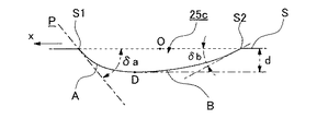
図10及び図11は、正反射方向に対して非対称の反射輝度分布を呈する本例の反射層に形成される多数の凹部25cの1つを示したもので、図10は、その斜視構成図であり、図11は、図10に示す特定縦断面Xにおける断面構成図である。
図10に示す凹部25cの特定縦断面Xにおいて、凹部25cの内面形状は、凹部60の一の周辺部S1から最深点Dに至る第1曲線Aと、この第1曲線Aに連続して、凹部の最深点Dから他の周辺部S2に至る第2曲線Bとからなっている。これら両曲線は、最深点Dにおいて共に反射膜表面Sに対する傾斜角がゼロとなり、互いにつながっている。
ここでの「傾斜角」とは、特定の縦断面において凹部の内面の任意の箇所における接線の、水平面(ここでは凹部が形成されていない部分の反射膜表面S)に対する角度のことである。
【0050】
第1曲線Aの反射膜表面Sに対する傾斜角は第2曲線Dの傾斜角よりも急であって、最深点Dは凹部25cの中心Oからx方向にずれた位置にある。すなわち、第1曲線Aの反射膜表面Sに対する傾斜角の絶対値の平均値は、第2曲線Bの反射膜表面Sに対する傾斜角の絶対値の平均値より大きくなっている。拡散性反射体の表面に形成されている複数の凹部25cにおける、第1の曲線Aの反射膜表面Sに対する傾斜角は、1〜89°の範囲で不規則にばらついている。また、凹部25cにおける第2曲線Bの反射膜表面Sに対する傾斜角の絶対値の平均値は0.5〜88°の範囲で不規則にばらついている。
両曲線の傾斜角は、いずれもなだらかに変化しているので、第1曲線Aの最大傾斜角δa(絶対値)は、第2曲線Bの最大傾斜角δb(絶対値)よりも大きくなっている。また、第1曲線Aと第2曲線Bとが接する最深点Dの基材表面に対する傾斜角はゼロとなっており、傾斜角が負の値である第1曲線Aと傾斜角が正の値である第2曲線Bとは、なだらかに連続している。
反射層25の表面に形成されている複数の凹部25cにおけるそれぞれの最大傾斜角δaは、2〜90°の範囲内で不規則にばらついているが、多くの凹部は最大傾斜角δaが4〜35°の範囲内で不規則にばらついている。
【0051】
また凹部25cは、その凹面が単一の極小点(傾斜角がゼロとなる曲面上の点)Dを有している。そしてこの極小点Dと基材の反射膜表面Sとの距離が凹部25cの深さdを形成し、この深さdは、複数の凹部25cについてそれぞれ0.1μm〜3μmの範囲内で不規則にばらついている。
また、本実施形態において、複数の凹部25cのそれぞれにおける特定断面Xは、いずれも同じ方向となっている。また各々の第1曲線Aが単一の方向に配向するように形成されている。すなわち、いずれの凹部でも、図10,11に矢印で示すx方向が同一方向を向くように形成されている。
【0052】
かかる構成の反射層25にあっては、複数の凹部25cにおける第1曲線Aが単一の方向に配向されているので、このような反射層25に対して、図11中のx方向(第1曲線A側)の斜め上方から入射した光の反射光は、正反射方向よりも反射膜表面Sの法線方向側にシフトする。
逆に、図11中のx方向と反対方向(第2曲線B側)の斜め上方から入射した光の反射光は、正反射方向よりも反射膜表面Sの表面側にシフトする。
したがって、特定縦断面Xにおける総合的な反射特性としては、第2曲線B周辺の面によって反射される方向の反射率が増加することになるので、これにより、特定の方向における反射効率を選択的に向上させた反射特性を得ることができる。
【0053】
本実施形態で用いられている反射層25の反射面(反射膜25b表面)に、上記x方向から入射角30°で光を照射し、受光角を、反射面に対する正反射の方向である30゜を中心として、垂線位置(0°;法線方向)から60°まで振ったときの受光角(単位:°)と明るさ(反射率、単位:%)との関係を図12に示す。また図12には、図8に示す断面形状の凹部25cを形成した場合の受光角と反射率の関係も併記する。図12に示すように、本例の構成とされた入射角度である30°の正反射方向である反射角度30°よりも、小さい反射角度における反射率が最も高くなり、その方向をピークとして近傍の反射率も高くなる。
【0054】
従って、かかる構成の反射層25によれば、その反射面をなす反射膜が上記のような形状とされているので、導光板12から出射された光を効率よく反射、散乱できるとともに、反射層25で反射される反射光は、特定の方向において反射率が高くなるという指向性を有しているので、これにより反射層25を経由して出射される反射光の出射角度が広くなるとともに、特定の出射角度において出射効率を向上させることができる。
【0055】
[反射層の第2変形例]
また、入射光の正反射方向に対して非対称の反射輝度分布としては、以下の構成の反射層も適用することができる。この構成を反射層の第2変形例として以下に説明する。
本例における反射層についても、上記第1変形例と同様に、図7に示す凹部25cの内面形状を変化させることにより形成することができる。すなわち、本例の反射層は、図7の斜視構成図に示す先の実施形態の反射層25と同様に、反射面側に多数の凹部25c重なり合うように隣接して形成された有機膜25a上に、高反射率の反射膜25bが成膜された構成を備えており、前記凹部25cの内面形状のみが異なるものである。従って、本例に係る反射層を構成する各部の説明に図7を併用することとする。
【0056】
図13〜15は、本実施形態で用いられる反射層25の反射膜25bの表面に形成される1つの凹部25cの内面形状を示したものである。
図13は、凹部25cの斜視図であり、図14は、凹部25cのX軸に沿う断面(縦断面Xという)、図15は、凹部25cのX軸と直交するY軸に沿う断面(縦断面Yという)をそれぞれ示している。
図14に示すように、凹部25cの縦断面Xにおける内面形状は、凹部25cの一つの周辺部S1から最深点Dに至る第1曲線A’と、この第1曲線に連続して、凹部の最深点Dから他の周辺部S2に至る第2曲線B’とからなるものである。図14において右下がりの第1曲線Aと右上がりの第2曲線Bとは、最深点Dにおいて共に反射膜表面Sに対する傾斜角がゼロとなり、互いに滑らかに連続している。
ここでの「傾斜角」とは、特定の縦断面において凹部の内面の任意の箇所における接線の、水平面(ここでは凹部が形成されていない部分の反射膜表面S)に対する角度のことである。
【0057】
第1曲線A’の反射膜表面Sに対する傾斜角は、第2曲線B’の傾斜角よりも急であって、最深点Dは、凹部25cの中心OからX軸に沿って周縁に向かう方向(x方向)にずれた位置にある。すなわち、第1曲線A’の傾斜角の絶対値の平均値は、第2曲線B’の傾斜角の絶対値の平均値よりも大きくなっている。反射層の表面に形成されている複数の凹部25cにおける第1曲線A’の傾斜角の絶対値の平均値は、2°〜90°の範囲で不規則にばらついており、また複数の凹部25cにおける第2曲線B’の傾斜角の絶対値の平均値も1°〜89°の範囲で不規則にばらついている。
【0058】
一方、図15に示すように、凹部25cの縦断面Yにおける内面形状は、凹部25cの中心Oに対してほぼ左右均等の形状を成しており、凹部25cの最深点Dの周辺は、曲率半径の大きい、すなわち、直線に近い浅型曲線Eとなっている。また、浅型曲線Eの左右は、曲率半径の小さい深型曲線F,Gとなっており、反射層25の表面に形成されている複数の凹部25cにおける前記浅型曲線Eの傾斜角の絶対値は、概ね10°以下である。また、これら複数の凹部25cにおける深型曲線F,Gの傾斜角の絶対値も不規則にばらついているが、例えば2°〜90°である。また、最深点Dの深さdは、0.1μm〜3μmの範囲内で不規則にばらついている。
【0059】
本例において、反射層25の表面に形成されている複数の凹部25cは、上記の縦断面Xの形状を与える断面方向がいずれも同一方向となり、かつ上記の縦断面Yの形状を与える断面方向がいずれも同一方向となるとともに、最深点Dから第1曲線A’を経て周辺部S1へ向かう方向がいずれも同一方向となるように配向されている。すなわち、反射層の表面に形成されている全ての凹部25cは、図13,14中に矢印で示したx方向が同一方向を向くように形成されている。
【0060】
本例においては、反射層25の表面に形成されている各凹部25cの向きが揃っており、最深点Dから第1曲線A’を経て周辺部S1へ向かう方向がいずれも同一であるので、この反射層25に対して、図13,14中のx方向(第1曲線A’側)の斜め上方から入射した光の反射光は、正反射方向よりも反射膜表面Sの法線方向側にシフトする。
逆に、図13,14中のx方向と反対方向(第2曲線B’側)の斜め上方から入射した光の反射光は、正反射方向よりも反射膜表面Sの表面側にシフトする。
また、縦断面Xと直交する縦断面Yは、曲率半径の大きい浅型曲線Eと、浅型曲線Eの両側にあって曲率半径の小さい深型曲線F,Gとを有するように形成されているので、これにより反射層25の反射面において正反射方向の反射率も高められる。
【0061】
その結果、図16に示すように、縦断面Xにおける総合的な反射特性としては、正反射方向の反射率を十分に確保しつつ、特定の方向に反射光を適度に集中させた反射特性とすることができる。図16は、本変形例に係る反射層に、反射膜表面Sの法線方向よりも前記x方向寄りの方向から入射角30°で光を照射し、視角を反射膜表面Sに対する正反射の方向である30°を中心として、垂線位置(0°)から60°まで連続的に変化させた場合の視角(θ°)と明るさ(反射率高さ)との関係を示したものである。このグラフで表される反射特性は、正反射の角度30゜より小さい反射角度範囲の反射率の積分値が、正反射の角度より大きい反射角度範囲の反射率の積分値より大きくなっており、反射方向が正反射方向よりも法線側にシフトする傾向にある。
【0062】
従って、上記構成の反射層25を備えた液晶表示ユニットによれば、反射層25の反射面をなす反射膜が上記のような形状とされているので、導光板12から出射された光を効率よく反射、散乱できるとともに、反射層25で反射される反射光は、特定の方向において反射率が高くなるという指向性を有しているので、これにより反射層25を経由して出射される反射光の出射角度が広くなるとともに、特定の出射角度において出射効率を高くすることができる。
【0063】
[アクティブマトリクス型液晶表示ユニット]
上述の実施形態では、液晶表示ユニット20をパッシブマトリクス型としたが、本発明に係る液晶表示装置には、アクティブマトリクス型の液晶表示ユニットも適用することができる。この場合にも、液晶表示ユニットの平面構成は、図2に示す先の実施形態の液晶表示ユニット20と同様であるので、以下の説明には図2も併用することとする。つまり、本構成の液晶表示ユニットは平面視マトリクス状に配列形成された複数の画素20cを備えている。
本構成の液晶表示ユニットに形成された画素20cの平面構成図を図17に示し、図17のH−H線に沿う断面構成図を図18に示す。図17、18に示す液晶表示ユニットは、対向して配置された上基板31と、下基板32との間に液晶層33を挟持して構成されており、上基板31の内面側に、平面視マトリクス状に配列形成された複数の略長方形状の透明電極36と、これら透明電極36毎に形成された画素スイッチング用のトランジスタ素子Tとを備えており、下基板32の内面側に、反射層35と、この反射層35上に形成されたカラーフィルタ層39と、このカラーフィルタ層39上の全面に形成された透明電極38とを備えている。そして、R,G,Bに対応する3つの透明電極36が形成された領域が、1画素20cに対応している。尚、図17では、図面を見易くするためにトランジスタ素子Tを等価回路図とした。
上記透明電極36をスイッチングするためのトランジスタ素子Tの一端側は、透明電極36に接続され、トランジスタ素子Tの他の二端は、透明電極36の間の図示左右方向に延在する走査線G1〜G3及び、図示上下方向に延在する信号線S1に接続されている。また、下基板32の前記透明電極36と対応する位置のカラーフィルタ層39には、それぞれカラーフィルタ39R,39G,39Bが配置され、隣接するカラーフィルタ39R,39G,39B間には、ブラックマトリクス39Mが平面視格子状に形成されている。また、図示は省略したが、上基板31の内面側にも、透明電極36の周囲を取り囲むように平面視格子状のブラックマトリクスが形成されており、上面側から入射する光がトランジスタ素子Tや、これに接続された走査線や信号線に入射しないようになっている。
また、本例の液晶表示ユニットの反射層35としては、先の実施形態で説明した構成の反射層のいずれも適用することができる。
【0064】
上記構成の液晶表示ユニットは、トランジスタ素子Tにより透明電極36の電位を制御し、透明電極36と下基板32の透明電極38との間の液晶層33の光透過状態を制御することで、表示を行うようになっている。
アクティブマトリクス型の液晶表示ユニットでは、透明電極26Aを取り囲むように遮光性のBM(ブラックマトリクス)が平面視格子状に形成され、また表示のコントラストを高くすることができるため、パッシブマトリクス型の液晶表示ユニットよりも、画素20cの周期的な模様が明瞭になる傾向がある。すなわち、画素20cの周期的配列と、フロントライト10のプリズム溝14との光学的干渉が生じやすくなる傾向となるが、本実施形態の液晶表示装置では、プリズム溝14が画素20cの配列方向と交差する向きに延在するように形成されていることで、前記干渉を抑制し、モアレ模様により視認性が低下するのを効果的に防止することができる。このように、アクティブマトリクス型の液晶表示ユニットを用いて本発明に係る液晶表示装置を構成した場合にも、その表示領域においてモアレ模様が生じることが無く、また均一で明るい表示が可能な表示品質に優れた液晶表示装置とすることができる。
【0065】
尚、図18には、反射層35側にカラーフィルタ層39を形成した場合を示したが、下基板32側に画素スイッチング用の電極を形成するとともに、この電極が反射層を兼ねる構成とし、上基板31側にカラーフィルタ層を形成して構成することもできる。
【0066】
(第2の実施形態)
次に、本発明の第2の実施形態の液晶表示装置について図19を参照して説明する。図19は、本実施形態の液晶表示装置の平面構成図である。この図に示す液晶表示装置は、フロントライト10Aと、その背面側に配設された反射型の液晶表示ユニット20とを備えて構成されている。フロントライト10Aは、導光板12Aとその側端面(入光面)12Bに沿って配設された中間導光体13Aと、中間導光体13Aの図示左側端面部に配設された発光素子15とを備えて構成されており、液晶表示ユニット20は、図1及び図3に示す液晶表示ユニットと同等のものであり、その表示領域20D内に複数の画素20cがマトリクス状に形成されている。
本実施形態の液晶表示装置の特徴的な点は、図19に示すように、フロントライト10Aの導光板12Aが、液晶表示ユニット20の表示領域20Dよりも大きく形成されるとともに、導光板12Aが、平面的に見て発光素子15側に液晶表示ユニット20より突出するように配置されている点にあり、上記以外の構成については、図2に示すフロントライト10と同様の構成であるため、以下ではその詳細な説明は省略することとする。
【0067】
図19に示すように、本実施形態の液晶表示装置においては、導光板12の図示左右方向の長さが、液晶表示ユニット20の表示領域20Dの中間導光体13延在方向への長さよりも大きい幅Wとされており、図19に示す延長幅ΔWだけ表示領域20Dよりも外側に配置されるようになっている。このような構成とされていることで、液晶表示ユニット20の表示領域20Dへの照明光の均一性を高め、視認性に優れる液晶表示装置を提供することができる。
すなわち、発光素子15が一つのみ設けられ、プリズム溝14が入光面12Bに対して傾斜して形成されたフロントライトにおいては、導光板12の発光素子15側の側端部側の出射光量が低下しやすい傾向があり、場合によっては図19に示すような平面視三角形状の暗部18が形成される場合がある。そこで、本実施形態のフロントライト10Aでは、導光板12Aの発光素子15側に生じる暗部(出射光量が周囲よりも少ない領域)18が、液晶表示ユニット20の表示領域20Dと重ならないようにし、導光板12の照明光が均一になる領域を表示に利用し、均一で明るい表示が得られるようしている。
【0068】
図19に示す1灯型のフロントライト10Aにおける暗部18は、導光板12の側方側端部に沿って、中間導光体13側は狭く、中間導光体13と反対側の導光板12端面に向かって広くなる三角形状となる。従って、この暗部18が液晶表示ユニット20の表示領域20Dと重ならないようにするためには、少なくとも、上記導光板の延長長さΔWが、導光板12の図示上側側端部(暗部18の幅が最も広くなる位置)において、暗部18の幅以上の長さとされることが好ましい。ただし、フロントライト10の導光板12の延長幅は、液晶表示装置の小型化や、製造コストの点から、可能な限り小さくすることが好ましい。本発明に係る導光板12の延長幅ΔWの下限値は、導光板のプリズム溝14の傾斜角αと、導光板12の長さLとを用いて、L×tanαなる長さとすることが好ましい。すなわち、上記暗部18は、導光板12のプリズム溝14の傾斜角αとほぼ相関関係にあり、傾斜角αを大きくするほど暗部18の幅も広くなる。これは、導光板12内部を伝搬する光が、プリズム溝14と直交する方向に伝搬しやすいことによる。このことから、暗部18の幅は、プリズム溝14の傾斜角αと、図示上下方向(導光方向)の導光板12の長さLとを用いた(式)L×tanαにほぼ等しくなると考えられ、上記導光板の延長幅ΔWを、少なくともL×tanα以上とすれば、暗部18は液晶表示ユニット20の表示領域20Dより外側に配置され、導光板12の照明光が均一な領域を表示に利用することができることになる。
【0069】
(第3の実施形態)
次に、本発明に係る照明装置の第3の実施形態として、図20に示すフロントライトについて説明する。
図20は、本発明に係る照明装置の第3の実施形態としてのフロントライトの平面構成図である。この図に示すフロントライト40は、導光板42と、その二側端面に沿って配設された平面視L型の中間導光体43と、この中間導光体43の端面部に配設された発光素子45とを備えて構成されている。
導光板42は、図1〜図3に示す先の実施形態の導光板12とほぼ同等の略平板状とされており、その一面側に、平面視互いに平行に複数のプリズム溝44が形成されており、他面側は平坦面とされている。そして、その側端面42a、42bから導入された光を、前記プリズム溝44により反射させて照明光を出射する構造とされている。また、上記プリズム溝44は、導光板42の側端面42aに対して傾斜して形成されており、1灯のみの発光素子45から出射された光を、導光板42面内で均一に伝搬させるようにするとともに、被照明物(液晶表示ユニットなど)との光学的干渉を防止するようになっている。このプリズム溝44の傾斜角度は、先の第1の実施形態におけるプリズム溝14の傾斜角αと同様とすることが好ましい。
【0070】
中間導光体43は、棒状の導光部43a、43bが、L字形に配置されて構成されており、導光部43aの導光部43bとの接続部側の端面部に、発光素子45が配設されている。そして、導光部43aは、導光板42の側端面42aに沿って配置され、導光部43bは、導光板42の側端面42bに沿って配設されている。また、図示を省略したが、導光板42と対向する導光部43a、43bの側面と反対側の側面には、図4に示す中間導光体13と同様の形状の平面視くさび状の溝が複数形成されている。また、この溝が形成された面には、必要に応じて反射膜を形成することもできる。
【0071】
上記構成の本実施形態のフロントライト40では、発光素子45から出射された光の大部分は、発光素子45が配設されている導光部43a内を伝搬し、導光板42の側端面42aから導光板42へ導入されるようになっている。そして、導光部43aに入射した光の一部が、導光部43bの基端部側の端面部43cから導光部43b内へ導入され、導光板42の側端面42bから導光板42へ導入されるようになっている。このような構成としたことで、本実施形態のフロントライト40は、1灯型のフロントライトにおいて出射光量の低下が生じやすい発光素子15側の側端部に対して、導光部43aと直交して配置された導光部43bにより光を導入することができる。従って、1灯型であっても導光板42の全面に渡って均一な出射光量を得ることができる。
【0072】
(第4の実施形態)
次に、本発明に係る照明装置の第4の実施形態として、図21に示すフロントライトについて説明する。
図21は、本発明の第4の実施形態であるフロントライトの平面構成図である。この図に示すフロントライト50は、導光板52と、その側端面52aに沿って配設された棒状の中間導光体53と、この中間導光体53の端面部に配設された発光素子55とを備えて構成されている。本実施形態のフロントライト50の特徴的な点は、発光素子55が配設された側の導光板側端面52bに、AlやAg等の高反射率の金属薄膜からなる反射膜57が形成されている点にある。
【0073】
導光板52は、図1〜図3に示す先の実施形態の導光板12とほぼ同等の略平板状とされており、その一面側に、平面視互いに平行に複数のプリズム溝54が形成されており、他面側は平坦面とされている。そして、その側端面52aから中間導光体53を介して導入された光を、前記プリズム溝54により反射させて照明光を出射する構造とされている。また、上記プリズム溝54は、導光板52の側端面52aに対して傾斜して形成されており、1灯のみの発光素子55から出射された光を、導光板52面内で均一に伝搬させるようにするとともに、被照明物(液晶表示ユニットなど)との光学的干渉を防止するようになっている。このプリズム溝54の入光面52aに対する傾斜角度は、先の第1の実施形態におけるプリズム溝14の傾斜角αと同様とすることが好ましい。
また、本実施形態に係る中間導光体53及び発光素子55としては、上記第1の実施形態に係る中間導光体13及び発光素子15と同一の構成のものを適用することができるので、その詳細な説明はここでは省略する。
【0074】
上記構成の本実施形態のフロントライト50によれば、1灯型のフロントライトにおいて出射光量の低下が生じやすい発光素子側の側端部に対して、当該側端部側の側端面52b上に反射膜57が形成されていることで、側端面52bから導光板52内部を伝搬する光が漏洩することが無く、また、反射膜57で反射された光は照明光として利用されるため、出射光量が低下しやすい部分の輝度を高めることができる。従って、本実施形態のフロントライト50によっても、1灯型であっても導光板52の全面に渡って均一な出射光量を得ることができる。
【0075】
(第5の実施形態)
次に、本発明に係る照明装置の第5の実施形態として、図22に示すフロントライトについて説明する。
図22は、本発明の第5の実施形態であるフロントライトの平面構成図である。この図に示すフロントライト60は、導光板62と、その側端面(入光面)62aに沿って配設された棒状の中間導光体63と、この中間導光体63の端面部に配設された発光素子65とを備えて構成されている。本実施形態のフロントライト60の特徴的な点は、その反射面に形成されたプリズム溝64の急斜面部64bの幅が、導光板の入光面62aから離れるに従って広くなるように形成されている点にある。
【0076】
導光板62は、図1〜図3に示す先の実施形態の導光板12とほぼ同等の略平板状とされており、その一面側に、平面視互いに平行に複数のプリズム溝64が形成されており、他面側は平坦面とされている。そして、その側端面(入光面)62aから中間導光体63を介して導入された光を、前記プリズム溝64により反射させて照明光を出射する構造とされている。また、上記プリズム溝64は、その延在方向が導光板52の側端面52aに対して傾斜するように形成されており、1灯のみの発光素子65から出射された光を、導光板62面内で均一に伝搬させるようにするとともに、被照明物(液晶表示ユニットなど)との光学的干渉を防止するようになっている。このプリズム溝64の入光面62aに対する傾斜角度は、先の第1の実施形態におけるプリズム溝14の傾斜角αと同様とすることが好ましい。
また、本実施形態に係る中間導光体63及び発光素子65としては、上記第1の実施形態に係る中間導光体13及び発光素子15と同一の構成のものを適用することができるので、その詳細な説明はここでは省略する。
【0077】
本実施形態に係る導光板62に形成されたプリズム溝64は、断面視くさび状に配置された緩斜面部64aと、この緩斜面部64aよりも急な傾斜角度に形成された急斜面部64bとから構成されており、1つのプリズム溝64において、急斜面部64bは、緩斜面部64aよりも導光板の入光面62a側に配置されている。また、前記緩斜面部64a及び急斜面部64bの傾斜角度は、上記第1の実施形態に係る緩斜面部14a及び急斜面部14bと同様の傾斜角度範囲とされている。
【0078】
そして、図22に示すように、本実施形態のフロントライト60では、プリズム溝64は一定のピッチでストライプ状に形成されているが、そのプリズム溝64を構成する緩斜面部64aと急斜面部64bの幅の比率が面内で連続的に変化するように形成されている。より詳細には、導光板の入光面62aに対して傾斜して形成されたプリズム溝64の延在方向において、入光面62aから離れるに従って、急斜面部64bの幅が連続的に広くなるように(緩斜面部64aの幅が狭くなるように)形成されている。このような構成とされていることで、本実施形態のフロントライト60は、入光面62aから離れるに従って、急斜面部64bにより落射される光の割合を増加させ、出射光量を導光板面内で均一にすることができるようになっている。
また、本実施形態のフロントライト60では、入光面62aからの距離が等しい位置におけるプリズム溝64の急斜面部64bの幅が複数のプリズム溝64で一定となるように形成されている。つまり、図22に示す直線D1とプリズム溝64とが交差する位置での急斜面部64aの幅は、直線D1に沿う導光板上で一定とされている。このような構成とされていることで、図示左右方向における出射光量のばらつきを抑えることができる。
【0079】
【実施例】
以下、実施例により本発明をより詳細に説明する。ただし、以下の実施例は本発明を限定するものではない。
【0080】
(実施例1)
本実施例では、図1〜図3に示す構成において、入光面12aの最近位置における急斜面部14bの幅と、最遠位置における急斜面部の幅との比率を種々に変化させたフロントライトをそれぞれ作製し、導光板面内における輝度分布を測定した。
【0081】
まず、樹脂材料を射出成形することにより、中間導光体と、導光板を作製した。中間導光体の材料にはアクリル樹脂を用い、36.3mm×3.0mm×1.0mmの四角柱状に成形するとともに、その一側面に先端角110°のV字状の溝を、0.24μmピッチで多数形成した。このV字状の溝は、中間導光体の発光素子が配設される側の端面部に近い溝ほど浅く形成し、より詳細には溝の深さが発光素子側から12μm〜71μmの範囲で順次深くなるように形成した。また、このV字状の溝が形成された中間導光体側面に、Ag薄膜からなる反射膜を、膜厚200nmとなるように形成した。次いで、上記中間導光体の一側の端面部に、LEDを配設した。このLEDには、NSCW215T(商品名:日亜化学社製)を用いた。
【0082】
導光板は、36.3mm(W)×50.2mm(L)×1.0mm(t)の大きさで、一面側に複数のプリズム溝が形成された図1に示す構成のものを作製した。成形材料としてはアートン(商品名:JSR社製)を用いた。その際、プリズム溝の延在方向と、中間導光体が配設される側端面との角度(傾斜角α)は0°とし、プリズム溝のピッチは0.16mmとした。また、プリズム溝を構成する二斜面部の傾斜角度は急斜面部を43°、緩斜面部を2.3°で共通とし、入光面12aの最近位置における急斜面部14bの幅と、最遠位置における急斜面部の幅との比率を表1に示すように種々に変化させた5種類の導光板を作製した。より具体的には、例えば表1に示すNo.1−3の導光板の場合には、入光面の最近位置における急斜面部の幅を7.91μmとし、最遠位置の急斜面部の幅を10.29μmとし、その間に形成される急斜面部については、前記両者の間を比例配分して形成した。すなわち、急斜面部の幅は入光面からの距離に比例するようにした。また、そのほかの導光板については、入光面の最近位置の急斜面部の幅は上記No.1−3のものと同じとし、それ以外のプリズム溝の急斜面部は表1に示す急斜面幅比に応じて変化させた。
次いで、上記にて得られたそれぞれの導光板の側端面に棒状の中間導光体を配設して本例のフロントライトを得た。
【0083】
次に、上記にて作製された各フロントライトを点灯させて、その輝度分布を測定した。その際、輝度の測定位置は各導光板で共通とし、図2を参照して説明すると、導光板12を図示上下方向に3領域に分割し、それぞれの領域の中心点を測定点とした。従って、表1に示す測定点2が導光板の中心に相当し、測定点1は、前記測定点2から図2上方向に約12.5mm離れた位置であり、測定点3は、前記測定点2から図2下方向に約12.5mm離れた位置である。
上記輝度測定の結果を表1に併記する。表1に示すように、各フロントライトのうち、急斜面幅比が、1.0:1.1〜1.0:1.5の範囲において、測定点間の輝度差は、22%以内に収まっており、実用上輝度分布が均一と見なせる範囲であった。
反射型の液晶表示装置のフロントライトとして用いた場合に、実用上問題ないとされる輝度分布は、25%程度であり、これ以上の輝度差が導光板面内で生じると、輝度が高すぎる(又は低すぎる)位置における視認性が著しく低下する。従って、急斜面幅比が1:1とされたNo.1−1のフロントライトは、測定点1における輝度が明らかに不足している。また、最遠位置の急斜面幅を大きくするほど測定点1の輝度が高くなる傾向にあり、No.1−5ではすでに測定点1と測定点3との輝度差が20%に到達しているため、急斜面幅比は1:1.5が上限であることが示唆される。
【0084】
【表1】

(実施例2)
次に、導光板の反射面に形成されるプリズム溝の急斜面部の傾斜角度による効果を明らかにするために、表2に示す傾斜角度θ1、θ2の緩斜面部及び急斜面部からなるプリズム溝を有する7種類の導光板を作製し、フロントライトを構成してその平均輝度を測定した。尚、本実施例の各フロントライトの作製工程は、上記実施例1のフロントライトと基本的には同様としたが、各フロントライトにおいて急斜面幅比を1.0:1.3で共通とし、プリズム溝の緩斜面部の傾斜角度θ1も2.3°で共通とした。
表2に、上記平均輝度の測定結果を併記する。表2に示すように、急斜面部の傾斜角度θ2が41°〜45°の範囲において、約15cd/cm2以上の平均輝度が得られており、前記範囲を超えると平均輝度が低下する傾向にある。従って、光源(発光素子)の利用効率を最大にし、高輝度のフロントライトを構成するには、急斜面部の傾斜角度を41°〜45°にするのが良いことが確認された。
【0086】
【表2】
(実施例3)
本実施例では、図1〜図3に示す構成のフロントライトを作製し、液晶表示ユニットの前面側に配設して液晶表示装置を作製した。そして、本発明の構成によればモアレ模様が生じにくく、かつ均一な明るさの表示を得られることを検証した。
【0088】
まず、樹脂材料を射出成形することにより、中間導光体と、導光板を作製した。中間導光体の材料にはアクリル樹脂を用い、73.5mm×4.8mm×1.0mmの四角柱状に成形するとともに、その一側面に先端角110°のV字状の溝を、0.24μmピッチで多数形成した。このV字状の溝は、中間導光体の発光素子が配設される側の端面部に近い溝ほど浅く形成し、より詳細には溝の深さが発光素子側から12μm〜71μmの範囲となるように形成した。また、このV字状の溝が形成された中間導光体側面に、Ag薄膜からなる反射膜を、膜厚200nmとなるように形成した。
次いで、上記中間導光体の一側の端面部に、LEDを配設した。このLEDには、NSCW215T(商品名:日亜化学社製)を用いた。
【0089】
導光板は、73.5mm(W)×50mm(L)×1.0mmの大きさで、一面側に複数のプリズム溝が形成された図1に示す構成のものを作製した。成形材料としてはアートン(商品名:JSR社製)を用いた。その際、プリズム溝のピッチを、表3に示すピッチとなるように種々に変えて形成したものを作製した。尚、本実施例では導光板と組み合わせて用いる液晶表示ユニット(後述する)の画素の配列方向と、導光板の側端面とはほぼ平行に配置したので、上記傾斜角αは、プリズム溝の延在方向と液晶表示ユニットの画素配列方向との成す角度(傾斜角β)と同一である。
また、これらの導光板において、プリズム溝を構成する二斜面部の傾斜角度は急斜面部を43°、緩斜面部を2.3°で共通とした。
【0090】
次に、上記にて得られた導光板の側端面に棒状の中間導光体を配設してフロントライトを構成した。
【0091】
次いで、上記フロントライトを液晶表示ユニットの前面側に配設して液晶表示装置を構成し、この液晶表示装置を動作させて、モアレ模様の目視観察と、発光素子が配設された側の導光板の暗部の目視観察を行った。導光板の暗部については、導光板の幅方向(図2左右方向)への暗部の幅を計測した。これらの評価結果も表3に併記する。
尚、液晶表示ユニットは、画素ピッチ0.255mmのアクティブマトリクス型カラー液晶表示ユニットを用いた。また、このアクティブマトリクス型の液晶表示ユニットにおけるカラーフィルタの配列は、図6に示す縦ストライプ型のものとした。
【0092】
表3に示すように、プリズム溝の傾斜角αを7.5°とした試料において、プリズム溝のピッチが、0.12を越えて、0.2未満とされたもの(試料No.3−2〜3−4)において良好な結果が得られており、液晶表示ユニットの画素ピッチが0.255mmに対して、画素ピッチの1/2を越えて3/4未満のピッチとするのが良いことが確認された。
【0093】
【表3】
【発明の効果】
以上、詳細に説明したように、本発明の照明装置は、光源と、該光源の光を一側端面から導入し、内部を伝搬する前記光を一面側から出射させる導光板とを備え、前記光が導入される側端面が入光面とされ、前記導光板の一面側には、緩斜面部と、該緩斜面部より急な傾斜角度を有する急斜面部とで形成される複数のプリズム溝が平面視ストライプ状に連続して形成されており、前記プリズム溝の緩斜面部の傾斜角度θ1が1°以上10°以下とされ、前記急斜面部の傾斜角度θ2が41°以上45°以下とされており、前記反射面における前記急斜面部の幅が、前記入光面から離れた位置ほど大きくなるように形成され、前記入光面の最近位置における急斜面部の幅を1.0としたとき、最遠位置における前記急斜面部の幅が1.1以上1.5以下とされた構成としたことで、前記プリズム溝の構造が最適化され、照明装置に配設された光源の利用効率を高めて、高輝度の照明を可能とするとともに、導光板面内における出射光量の均一性を高めることができる。
【0095】
次に、本発明に係る液晶表示装置は、本発明の照明装置と、該照明装置の導光板出射面側に配設された液晶表示ユニットとを備えたことで、高輝度で明るさが均一な優れた表示品質を得ることができる。また、照明装置の発光素子を1灯とした場合にも、明るさの均一性が低下することがないため、優れた表示品質でかつ低消費電力の液晶表示装置とすることができる。
【図面の簡単な説明】
【図1】 図1は、本発明の第1の実施形態である液晶表示装置の斜視構成図である。
【図2】 図2は、図1に示す液晶表示装置の平面構成図である。
【図3】 図3は、図1に示す液晶表示装置の断面構成図である。
【図4】 図4は、図2に示す中間導光体を拡大して示す平面構成図である。
【図5】 図5は、図1に示すフロントライトの部分断面図である。
【図6】 図6は、図2に示す液晶表示ユニットの画素群を拡大して示す平面構成図である。
【図7】 図7は、図3に示す反射層の斜視構成図である。
【図8】 図8は、図7に示す凹部の断面形状を示す説明図である。
【図9】 図9は、図8に示す凹部を備えた反射層の反射特性を示す図である。
【図10】 図10は、反射層の第1変形例における凹部を示す斜視図である。
【図11】 図11は、図10に示す縦断面Xに沿う断面図である。
【図12】 図12は、図10,11に示す凹部を備えた反射層の反射特性を示す図である。
【図13】 図13は、反射層の第2変形例における凹部を示す斜視図である。
【図14】 図14は、図13に示す縦断面Xに沿う断面図である。
【図15】 図15は、図13に示す縦断面Yに沿う断面図である。
【図16】 図16は、図13〜15に示す凹部を備えた反射層の反射特性を示す図である。
【図17】 図17は、アクティブマトリクス型の液晶表示ユニットの画素を拡大して示す平面構成図である。
【図18】 図18は、図17のH−H線に沿う断面図である。
【図19】 図19は、本発明の第2の実施形態のフロントライトの平面構成図である。
【図20】 図20は、本発明の第3の実施形態のフロントライトの平面構成図である。
【図21】 図21は、本発明の第4の実施形態のフロントライトの平面構成図である。
【図22】 図22は、本発明の第5の実施形態のフロントライトの平面構成図である。
【図23】 図23Aは、従来の構成の液晶表示装置の斜視図であり、図23Bは、図23Aに示すフロントライトの平面図である。
【符号の説明】
10,40,50,60 フロントライト(照明装置)
20 液晶表示ユニット(被照明物)
20c 画素
20D 表示領域
12,42,52,62 導光板
12a 入光面(側端面)
12b 出射面
12c 反射面
13,43,53,63 中間導光体
14,44,54,64 プリズム溝
15,45,55,65 発光素子
14a,64a 緩斜面部
14b,64b 急斜面部
13b 溝
17 反射膜
25 反射層
43a、43b 導光部
57 反射膜[0001]
BACKGROUND OF THE INVENTION
The present invention relates to an illuminating device and a liquid crystal display device, and more particularly to an illuminating device capable of uniformly and brightly illuminating a wide area with a single light source, and a configuration of a liquid crystal display device using the illuminating device.
[0002]
[Prior art]
Conventionally, a unit composed of a light source, an intermediate light guide, a light guide plate, and a case body in which an inner surface for integrally holding them is made reflective is used for a front light of a reflective liquid crystal display device.
FIG. 23A is a perspective configuration diagram showing the liquid crystal display device having such a configuration, and FIG. 23B is a cross-sectional configuration diagram of the liquid crystal display device shown in FIG. 23A. The liquid crystal display device shown in these drawings includes a liquid
[0003]
The
The
[0004]
[Problems to be solved by the invention]
In portable electronic devices such as portable information terminals and portable game machines, the battery drive time greatly affects the usability, so in the liquid crystal display devices used as these display units, for the purpose of reducing the power consumption of the front light, As in the
[0005]
However, with such a one-lamp type front light, it is almost impossible to uniformly and brightly illuminate a wide area of a display screen of several inches or more by a combination of a thin light guide plate and one light-emitting element. It was. That is, in the
In addition, when the
[0006]
As described above, although there is an increasing demand for a front light that uses a single light emitting element as a light source, a front light that can illuminate a large area uniformly and brightly while being thin has not been realized. It was.
[0007]
The present invention has been made to solve the above-described problem, and an object of the present invention is to provide a low power consumption lighting device capable of uniformly and brightly illuminating a large area.
Another object of the present invention is to provide a liquid crystal display device having the above-described illumination device and having high luminance and excellent display quality.
[0008]
[Means for Solving the Problems]
In order to achieve the above object, the present invention employs the following configuration.
An illumination device according to the present invention includes a light source and a light guide plate that introduces light from the light source from one side end surface and emits the light propagating through the inside from one side, and the side end surface into which the light is introduced is A plurality of prism grooves formed by a gentle slope part and a steep slope part having a steeper slope angle than the gentle slope part are formed in a stripe shape in plan view on the one surface side of the light guide plate. The inclination angle of the gentle slope portion of the prism groove is 1 ° or more and 10 ° or less, the inclination angle of the steep slope portion is 41 ° or more and 45 ° or less, and the inclination angle of the steep slope portion is Above Incident surface The largest prism groove on the side, Incident surface The width of the steep slope portion is formed so as to increase as the distance from the light incident surface increases, and the width of the steep slope portion at the nearest position of the light entrance surface is the largest. The ratio of the width of the steep slope at the far position is in the range of 1.0: 1.1 to 1.0: 1.5, and the depth of the plurality of prism grooves on the one surface is constant. And the pitch of the plurality of prism grooves is constant. It is characterized by that.
According to the above configuration, the shape and size of the prism grooves formed on the reflecting surface side of the light guide plate are set in the above range, so that the amount of emitted light is uniform within the light guide plate surface and the light source utilization efficiency And a high-luminance lighting device can be obtained.
If the range of the inclination angle θ1 of the gentle slope portion is less than 1 °, sufficient luminance as an illuminating device cannot be obtained, and if it exceeds 10 °, the uniformity of the amount of light emitted from the exit surface of the light guide plate decreases. This is not preferable.
Further, when the inclination angle θ2 of the steep slope portion is less than 41 ° or more than 45 °, the luminance of the lighting device decreases, which is not preferable.
The width of the steep slope portion indicates the width of the slope portion in a direction orthogonal to the extending direction of the prism groove. The larger the width of the steep slope portion, the more the light is incident on the prism groove. Becomes larger. Therefore, in the illuminating device having this configuration, the width of the steep slope portion is formed to be an appropriate width according to the distance from the light guide plate incident surface. More specifically, in the vicinity of the light incident surface where the amount of light propagating through the light guide plate is relatively large, the ratio of the incident light is reduced by reducing the width of the steep slope portion relatively, and conversely the light incident surface. By increasing the width of the steep slope portion at a position away from the light, the proportion of light that is apologized is increased, so that the distribution of the emitted light amount as a whole of the light guide plate is made uniform.
The width of the steep slope portion in the present invention is the width of the steep slope portion formed at the position farthest from the light entrance surface when the width of the steep slope portion formed closest to the light entrance surface is 1.0. When the value is within the range of 1.1 to 1.5, the distribution of the emitted light quantity becomes uniform.
In addition, this inventor verifies in the below-mentioned Example that the setting range of the inclination-angle of the said slope part and the width | variety of a steep slope part is appropriate.
[0009]
Next, in the illumination device according to the present invention, the steep slope portions of the plurality of prism grooves are formed to have substantially the same width along the extending direction of the prism grooves, and an average distance from the light incident surface is It can be set as the structure where the width | variety of the said steep slope part is formed large, so that a prism groove is large.
That is, in the illumination device of this configuration, the prism groove having the width of the steep slope portion having a large width is formed sequentially from the prism groove closest to the light entrance surface of the light guide plate, and the steep slope portion of the prism groove farthest from the light entrance surface Is a lighting device whose width is 1.1 to 1.5 times the width of the steep slope at the nearest position. By adopting such a configuration, since the proportion of the light incident on the steep slope portion increases as the prism groove is located farther from the light incident surface of the light guide plate, the amount of light emitted within the light guide plate surface is made uniform. Can do.
[0010]
Next, the illuminating device according to the present invention may be configured such that the extending direction of the prism groove is in a direction intersecting with the light incident surface.
With such a configuration, when the object illuminated by the illumination device has a periodic shape or pattern with a predetermined interval, the prism groove of the light guide plate and the shape of the object to be illuminated Or it can suppress that a pattern interferes optically and a moire pattern arises. For example, when the object to be illuminated is a liquid crystal display unit, there may be a problem of optical interference between the arrangement of pixels formed in a matrix and the prism grooves. Generation of such moire patterns can be suppressed and excellent visibility can be obtained.
[0011]
Next, in the illumination device according to the present invention, the width of the steep slope portion of the prism groove may be formed so as to continuously increase from the side closer to the light incident surface toward the side farther from the light incident surface. it can.
With such a configuration, when the prism groove is formed in a direction intersecting with the light incident surface, the steep slope portion at a position away from the light incident surface can have a larger width. As the distance from the light incident surface increases, the ratio of incident light can be increased, and the amount of light emitted within the light guide plate surface can be made uniform.
[0012]
Next, in the illumination device according to the present invention, the inclination angle α of the prism groove formed by the extending direction of the prism groove and the length direction of the light incident surface is in the range of more than 0 ° and not more than 15 °. It is preferable that the inclination angle α of the prism groove is in the range of 6.5 ° to 8.5 °.
By setting it as such a structure, the uniformity of the emitted light quantity in a light-guide plate surface direction can be improved. In addition, optical interference between the object to be illuminated and the light guide plate can be more effectively suppressed. In particular, the periodic shape or pattern of the object to be illuminated is a shape or pattern including a straight line portion parallel to the light incident surface of the light guide plate, and the periodic repetition direction is orthogonal to the light guide plate incident surface. A more remarkable effect can be obtained when the direction is set.
If the inclination angle α of the prism groove is 0 ° or less or exceeds 15 °, the above effect cannot be obtained. In addition, by setting the inclination angle α of the prism groove to 6.5 ° or more and 8.5 ° or less, the illumination device has a more uniform distribution of emitted light quantity and is less likely to generate a moire pattern with an object to be illuminated. can do.
[0013]
Next, in the illumination device according to the present invention, the light source includes two light sources arranged in an L shape in plan view along a light incident surface of the light guide plate and a light guide plate side end surface adjacent to the light incident surface. An intermediate light guide composed of a light guide and a light emitting element disposed at the base end of the two light guides can be provided.
With such a configuration, light can be supplied from the two side end surfaces of the light guide plate, and the light guide plate end on the light emitting element side, in which the amount of emitted light is likely to decrease in the conventional one-lamp illumination device Since more light is supplied to the part, the uniformity of the emitted light quantity in the light guide plate surface can be improved.
[0014]
Next, in the illumination device according to the present invention, the light source includes an intermediate light guide disposed along a light incident surface of the light guide plate, and a light emitting element disposed on an end surface portion of the intermediate light guide. And a metal reflection film may be formed on the side end surface adjacent to the light incident surface of the light guide plate.
According to the illuminating device having the above configuration, the reflection film is disposed on the light guide plate side end surface adjacent to the light incident surface, and in particular, light leaks from the light guide plate side end surface on the light emitting element side to the outside. Since the light reflected by this reflective film returns to the light guide plate side, it is possible to effectively prevent a decrease in the amount of emitted light particularly at the end of the light guide plate on the light emitting element side, and excellent uniformity of the emitted light amount Can be obtained.
[0015]
Next, in the illumination device according to the present invention, the light source includes an intermediate light guide disposed along a light incident surface of the light guide plate, and a light emitting element disposed on an end surface portion of the intermediate light guide. In the surface of the light guide plate, a region where an object to be illuminated illuminated by the illumination device is transmitted and displayed is a display region, and the light guide plate is in the length direction of the light incident surface. In addition, the display area may be extended.
The illuminating device having the above configuration is used as a display region by extending the light emitting element side portion of the light guide plate, which is a position where the amount of emitted light is likely to decrease, in the surface of the light guide plate, in the extending direction of the intermediate light guide. From this range, the portion where the amount of emitted light is reduced is excluded, and an illumination device having a substantially uniform amount of emitted light is provided. The display area in the illumination device of the present invention is an area in the surface of the light guide plate where the object to be illuminated arranged on the back side of the illumination device is displayed through the light guide plate, and substantially An area on the light guide plate corresponding to a planar view outline of the object to be illuminated or a display area of the object to be illuminated.
[0016]
Next, in the illumination device according to the present invention, the extension width of the light guide plate is ΔW, the extension width ΔW, the inclination angle α of the prism groove, and the light guide plate side end surface adjacent to the light incident surface. And the length L satisfies the relationship of ΔW ≧ L × tan α.
The illuminating device having the above configuration reliably sets the dark portion generated on the light emitting element side of the light guide plate outside the display region of the light guide plate by setting the extended length of the light guide plate so as to satisfy the above relational expression. Therefore, it is possible to provide an illumination device that is excellent in the uniformity of the amount of emitted light in the display region.
[0017]
Next, in the illuminating device according to the present invention, the outer surface of the intermediate light guide is a prism surface in which a plurality of wedge-shaped grooves are formed, and a reflective film is formed on the surface of the prism surface. It is preferable that
The light incident on the intermediate light guide from the light emitting element propagates inside the intermediate light guide, is reflected by the prism surface, is emitted from the surface facing the prism surface, and enters the light guide plate. Yes. According to the said structure, the reflective film is formed in the said prism surface, The reflectance in a prism surface can be improved and the light quantity reflected toward a light-guide plate can be increased. Thereby, the light quantity which injects into a light-guide plate increases, As a result, the brightness | luminance of an illuminating device can be raised.
[0018]
Next, a liquid crystal display device according to the present invention includes any one of the illumination devices described above and a liquid crystal display unit illuminated by the illumination device.
The liquid crystal display device having the above configuration is provided with an illuminating device that can illuminate a large area uniformly and with high luminance, so that excellent display quality with high luminance and uniform brightness can be obtained. In addition, even when the light emitting element of the lighting device is a single lamp, the uniformity of brightness does not decrease, so that a liquid crystal display device with excellent display quality and low power consumption can be obtained.
[0019]
Next, in the liquid crystal display device according to the present invention, the illumination device is disposed on the front side of the liquid crystal display unit, and the pitch P1 of the prism grooves of the light guide plate is equal to the pixel pitch P0 of the liquid crystal display unit. On the other hand, the range is (1/2) P0 <P1 <(3/4) P0.
By setting the pixel pitch P0 of the liquid crystal display unit and the pitch P1 of the prism grooves so as to satisfy the above relationship, optical interference due to these periodic structures can be suppressed. Therefore, it is possible to prevent the visibility of the liquid crystal display device from being lowered.
When the pitch P1 of the prism grooves is (1/2) P0 or less, or (3/4) P0 or more, a moire pattern due to interference between the two tends to occur.
[0020]
Next, in the liquid crystal display device according to the present invention, an angle β formed between the extending direction of the prism grooves and the arrangement direction of the pixels of the liquid crystal display device along the light guide plate incident surface exceeds 0 °. The angle β is preferably in the range of 15 ° or less, and the angle β is more preferably in the range of 6.5 ° to 8.5 °.
That is, the angle β is an inclination angle with respect to the pixel arrangement direction of the prism grooves. When the inclination angle β is 0 ° or less, it is difficult to obtain the effect of suppressing the moire pattern. Further, when the angle exceeds 15 °, the display luminance is lowered, and there is a disadvantage that a dark portion on the light guide plate of the lighting device becomes large. Further, by setting the tilt angle β to 6.5 ° or more and 8.5 ° or less, it is possible to almost completely suppress optical interference, and it is possible to realize a liquid crystal display device that is extremely excellent in visibility. The angle β formed by the prism groove in this configuration and the pixel arrangement direction of the liquid crystal display unit is determined when the pixel arrangement direction of the liquid crystal display unit and the light incident surface of the light guide plate of the illumination device are arranged in parallel. The angle is the same as the previous prism groove inclination angle α.
[0021]
Next, in the liquid crystal display device according to the present invention, the liquid crystal display unit includes an upper substrate and a lower substrate arranged to face each other, and liquid crystal molecules having positive dielectric anisotropy sandwiched between the upper and lower substrates. And a reflective layer and a color filter are laminated on the inner surface side of the lower substrate, and the reflective layer is 10 ° or more and 40 ° or less with respect to the normal line of the display surface of the liquid crystal display unit. In the reflection angle range, the reflection luminance is substantially constant, and the reflection characteristic is provided.
With such a configuration, a display with a constant luminance can be obtained with a wide viewing angle, so that a liquid crystal display device with excellent usability can be realized.
[0022]
Next, the liquid crystal display device according to the present invention is characterized in that the reflection layer has a reflection characteristic in which the reflection luminance is distributed almost symmetrically about the regular reflection angle of incident light.
With such a configuration, a liquid crystal display device in which reflected light is diffused within a predetermined angle range from the regular reflection direction of incident light can be obtained.
[0023]
Next, the liquid crystal display device according to the present invention is characterized in that the reflection layer has a reflection characteristic in which reflection luminance is distributed asymmetrically with respect to a regular reflection angle of incident light.
With such a configuration, the brightness of reflected light (display light) in a predetermined direction can be increased. For example, when the user is used in a state in which the user does not face the regular reflection direction of the liquid crystal display device. In addition, the luminance toward the user can be ensured, and the liquid crystal display device can be more excellent in usability.
[0024]
Next, the liquid crystal display device according to the present invention is characterized in that the liquid crystal display unit is an active matrix type liquid crystal display unit.
Next, the liquid crystal display device according to the present invention is characterized in that the liquid crystal display unit is a passive matrix liquid crystal display unit.
In any of the liquid crystal display devices having the above-described configuration, the illumination device according to the present invention is provided on the front surface of the liquid crystal display unit, so that high-quality display with uniform brightness over the entire display area and no moire pattern can be achieved. Obtainable.
[0025]
DETAILED DESCRIPTION OF THE INVENTION
Hereinafter, embodiments of the present invention will be described with reference to the drawings.
(First embodiment)
[Overall configuration of liquid crystal display device]
1 is a perspective configuration diagram of a liquid crystal display device according to a first embodiment of the present invention, FIG. 2 is a plan configuration diagram of the liquid crystal display device shown in FIG. 1, and FIG. 3 is a liquid crystal display shown in FIG. It is a section lineblock diagram of an apparatus. As shown in FIGS. 1 to 3, the liquid crystal display device of the present embodiment includes a front light (illumination device) 10 and a reflective liquid
As shown in FIG. 1, the
The liquid
In the liquid crystal display device having the above configuration, the
[0026]
Next, the configuration of each part of the liquid crystal display device of the present embodiment will be described in detail with reference to the drawings.
[Front light]
The
[0027]
In the
[0028]
Further, in the
With this configuration, the
[0029]
The width of the steeply sloped
[0030]
The pitch P1 of the prism grooves 14 (the interval between the bottom tops of the prism grooves 14) is constant within the light guide
As described above, the pitch P1 and the depth of the
The pitch P1 and the depth of the
[0031]
In the
[0032]
As a material constituting the
Further, the
[0033]
The intermediate
A
The intermediate
[0034]
As shown in FIG. 1, a
In FIG. 5, the
[0035]
[LCD unit]
The liquid
The
[0036]
The
[0037]
In the liquid crystal display device of this embodiment, the extending direction of the
[0038]
6 is an enlarged plan view showing adjacent pixel groups of the liquid
The inclination angle β of the
[0039]
In the liquid crystal display device of the present embodiment, as shown in FIG. 2, the light guide plate side end surface 12 a of the
[0040]
Further, the liquid
[0041]
Next, the
The
[0042]
In the present embodiment, it is preferable that the
In the present embodiment, the
In this specification, “the depth of the recess” means the distance from the surface of the
[0043]
In the present embodiment, it is particularly important that the inclination angle distribution of the inner surface of the
If the depth of the
[0044]
Moreover, it is desirable that the pitch between the
[0045]
FIG. 9 shows the position of the perpendicular line with light incident from the display surface (upper surface) side of the liquid
[0046]
Thus, the reason why the reflectance can be made substantially constant in a wide light receiving angle range symmetric about the regular reflection direction is that the depth and pitch of the
[0047]
[First Modification of Reflective Layer]
In the liquid
[0048]
The reflection layer having the above-described reflection characteristics can be formed by changing the shape of the inner surface of the
[0049]
10 and 11 show one of a large number of
In the specific longitudinal section X of the
Here, the “inclination angle” is an angle of a tangent line at an arbitrary position on the inner surface of the concave portion with respect to a horizontal plane (here, the reflection film surface S in a portion where no concave portion is formed) in a specific longitudinal section.
[0050]
The inclination angle of the first curve A with respect to the reflection film surface S is steeper than the inclination angle of the second curve D, and the deepest point D is at a position shifted from the center O of the
Since the inclination angles of both curves change smoothly, the maximum inclination angle δa (absolute value) of the first curve A is larger than the maximum inclination angle δb (absolute value) of the second curve B. Yes. Further, the inclination angle of the deepest point D where the first curve A and the second curve B are in contact with the substrate surface is zero, and the first curve A and the inclination angle having a negative inclination angle are positive values. The second curve B is smoothly continuous.
The maximum inclination angle δa of each of the plurality of
[0051]
In addition, the concave surface of the
In the present embodiment, the specific cross section X in each of the plurality of
[0052]
In the
On the contrary, the reflected light of the light incident from diagonally above in the direction opposite to the x direction in FIG. 11 (the second curve B side) is shifted to the surface side of the reflective film surface S from the regular reflection direction.
Therefore, as a total reflection characteristic in the specific longitudinal section X, the reflectance in the direction reflected by the surface around the second curve B is increased, so that the reflection efficiency in the specific direction is selectively selected. It is possible to obtain improved reflection characteristics.
[0053]
The reflecting surface (the surface of the reflecting
[0054]
Therefore, according to the
[0055]
[Second Modification of Reflective Layer]
Moreover, as a reflection luminance distribution asymmetric with respect to the regular reflection direction of incident light, a reflection layer having the following configuration can also be applied. This configuration will be described below as a second modification of the reflective layer.
The reflective layer in this example can also be formed by changing the shape of the inner surface of the
[0056]
13 to 15 show the inner shape of one
13 is a perspective view of the
As shown in FIG. 14, the inner surface shape of the
Here, the “inclination angle” is an angle of a tangent line at an arbitrary position on the inner surface of the concave portion with respect to a horizontal plane (here, the reflection film surface S in a portion where no concave portion is formed) in a specific longitudinal section.
[0057]
The inclination angle of the first curve A ′ with respect to the reflection film surface S is steeper than the inclination angle of the second curve B ′, and the deepest point D is a direction from the center O of the
[0058]
On the other hand, as shown in FIG. 15, the inner surface shape of the longitudinal section Y of the
[0059]
In this example, the plurality of
[0060]
In this example, the direction of each
On the contrary, the reflected light of the light incident from obliquely above in the direction opposite to the x direction (second curve B ′ side) in FIGS. 13 and 14 is shifted to the surface side of the reflective film surface S from the regular reflection direction.
Further, the longitudinal section Y orthogonal to the longitudinal section X is formed to have a shallow curve E having a large curvature radius and deep curves F and G having a small curvature radius on both sides of the shallow curve E. As a result, the reflectance in the regular reflection direction on the reflection surface of the
[0061]
As a result, as shown in FIG. 16, the overall reflection characteristics in the longitudinal section X include a reflection characteristic in which reflected light is appropriately concentrated in a specific direction while sufficiently ensuring the reflectance in the regular reflection direction. can do. In FIG. 16, the reflective layer according to the present modification is irradiated with light at an incident angle of 30 ° from the direction closer to the x direction than the normal direction of the reflective film surface S, and the viewing angle is specularly reflected with respect to the reflective film surface S. This shows the relationship between the viewing angle (θ °) and brightness (reflectance height) when continuously changing from the perpendicular position (0 °) to 60 ° around the direction of 30 °. . In the reflection characteristics represented by this graph, the integral value of the reflectance in the reflection angle range smaller than the regular reflection angle of 30 ° is larger than the integral value of the reflectance in the reflection angle range larger than the regular reflection angle. The reflection direction tends to shift to the normal side with respect to the regular reflection direction.
[0062]
Therefore, according to the liquid crystal display unit including the
[0063]
[Active matrix type liquid crystal display unit]
In the above embodiment, the liquid
FIG. 17 shows a plan view of the
One end side of the transistor element T for switching the
In addition, as the
[0064]
The liquid crystal display unit having the above configuration controls the potential of the
In the active matrix liquid crystal display unit, a light-shielding BM (black matrix) is formed in a plan view lattice shape so as to surround the transparent electrode 26A, and the display contrast can be increased. The periodic pattern of the
[0065]
FIG. 18 shows a case where the color filter layer 39 is formed on the
[0066]
(Second Embodiment)
Next, a liquid crystal display device according to a second embodiment of the present invention will be described with reference to FIG. FIG. 19 is a plan configuration diagram of the liquid crystal display device of the present embodiment. The liquid crystal display device shown in this figure includes a
A characteristic point of the liquid crystal display device of the present embodiment is that, as shown in FIG. 19, the
[0067]
As shown in FIG. 19, in the liquid crystal display device of the present embodiment, the length of the
That is, in the front light in which only one
[0068]
The
[0069]
(Third embodiment)
Next, the front light shown in FIG. 20 is demonstrated as 3rd Embodiment of the illuminating device based on this invention.
FIG. 20 is a plan configuration diagram of a front light as a third embodiment of the illumination device according to the present invention. The front light 40 shown in this figure is provided on a
The
[0070]
The intermediate
[0071]
In the
[0072]
(Fourth embodiment)
Next, the front light shown in FIG. 21 is demonstrated as 4th Embodiment of the illuminating device based on this invention.
FIG. 21 is a plan configuration diagram of a front light according to the fourth embodiment of the present invention. The front light 50 shown in this figure includes a
[0073]
The
In addition, as the intermediate
[0074]
According to the
[0075]
(Fifth embodiment)
Next, the front light shown in FIG. 22 is demonstrated as 5th Embodiment of the illuminating device based on this invention.
FIG. 22 is a plan configuration diagram of a front light according to the fifth embodiment of the present invention. A
[0076]
The
Further, as the intermediate
[0077]
The
[0078]
As shown in FIG. 22, in the
Further, the
[0079]
【Example】
Hereinafter, the present invention will be described in more detail with reference to examples. However, the following examples do not limit the present invention.
[0080]
(Example 1)
In this embodiment, in the configuration shown in FIGS. 1 to 3, the front light in which the ratio between the width of the
[0081]
First, an intermediate light guide and a light guide plate were produced by injection molding of a resin material. Acrylic resin is used as the material of the intermediate light guide, and it is formed into a 36.3 mm × 3.0 mm × 1.0 mm square column shape. Many were formed at a pitch of 24 μm. The V-shaped groove is formed shallower in the groove closer to the end surface portion on the side where the light-emitting element of the intermediate light guide is disposed, and more specifically, the groove depth ranges from 12 μm to 71 μm from the light-emitting element side. It was formed so as to become deeper in order. In addition, a reflective film made of an Ag thin film was formed on the side surface of the intermediate light guide having the V-shaped groove so as to have a film thickness of 200 nm. Next, an LED was disposed on one end face of the intermediate light guide. NSCW215T (trade name: manufactured by Nichia Corporation) was used for this LED.
[0082]
The light guide plate has a size of 36.3 mm (W) × 50.2 mm (L) × 1.0 mm (t), and has a configuration shown in FIG. 1 in which a plurality of prism grooves are formed on one surface side. . Arton (trade name: manufactured by JSR) was used as the molding material. At that time, the angle (inclination angle α) between the extending direction of the prism grooves and the side end surface on which the intermediate light guide is disposed was 0 °, and the pitch of the prism grooves was 0.16 mm. The slopes of the two slopes constituting the prism groove are the same at 43 ° for the steep slope and 2.3 ° for the gentle slope, and the width of the
Next, a bar-shaped intermediate light guide was provided on the side end face of each light guide plate obtained above to obtain the front light of this example.
[0083]
Next, each front light produced above was turned on, and the luminance distribution was measured. At that time, the measurement position of the luminance is common to each light guide plate, and will be described with reference to FIG. 2. The
The results of the luminance measurement are also shown in Table 1. As shown in Table 1, the brightness difference between measurement points is within 22% when the steep slope width ratio is 1.0: 1.1 to 1.0: 1.5 among the front lights. In practice, the luminance distribution was in a range that could be considered uniform.
When used as a front light of a reflective liquid crystal display device, the luminance distribution considered to be a practical problem is about 25%. If a luminance difference larger than this occurs in the light guide plate surface, the luminance is too high. The visibility at the position (or too low) is significantly reduced. Therefore, the No. 1 steep slope width ratio is set to 1: 1. The front light of 1-1 clearly lacks the luminance at the
[0084]
[Table 1]
(Example 2)
Next, in order to clarify the effect of the inclination angle of the steep slope portion of the prism groove formed on the reflection surface of the light guide plate, the prism groove comprising the gentle slope portion and the steep slope portion of the inclination angles θ1 and θ2 shown in Table 2 is provided. Seven types of light guide plates were prepared, a front light was constructed, and the average luminance was measured. In addition, although the manufacturing process of each front light of the present embodiment is basically the same as the front light of the first embodiment, the steep slope width ratio is 1.0: 1.3 in each front light, The inclination angle θ1 of the gentle slope portion of the prism groove is also 2.3 °.
Table 2 shows the measurement results of the average luminance. As shown in Table 2, when the inclination angle θ2 of the steep slope portion is in the range of 41 ° to 45 °, it is about 15 cd / cm. 2 The above average luminance is obtained, and when it exceeds the above range, the average luminance tends to decrease. Therefore, in order to maximize the utilization efficiency of the light source (light emitting element) and to construct a high-luminance front light, it was confirmed that the inclination angle of the steep slope portion should be 41 ° to 45 °.
[0086]
[Table 2]
(Example 3)
In this example, a front light having the configuration shown in FIGS. 1 to 3 was manufactured and disposed on the front side of the liquid crystal display unit to manufacture a liquid crystal display device. And it verified that according to the structure of this invention, a moire pattern was hard to produce and the display of uniform brightness was obtained.
[0088]
First, an intermediate light guide and a light guide plate were produced by injection molding of a resin material. The intermediate light guide is made of acrylic resin and is formed into a 73.5 mm × 4.8 mm × 1.0 mm square column shape, and a V-shaped groove with a tip angle of 110 ° is formed on one side of the intermediate light guide. Many were formed at a pitch of 24 μm. The V-shaped groove is formed shallower in the groove closer to the end surface portion on the side where the light-emitting element of the intermediate light guide is disposed, and more specifically, the groove depth ranges from 12 μm to 71 μm from the light-emitting element side. It formed so that it might become. In addition, a reflective film made of an Ag thin film was formed on the side surface of the intermediate light guide having the V-shaped groove so as to have a film thickness of 200 nm.
Next, an LED was disposed on one end face of the intermediate light guide. NSCW215T (trade name: manufactured by Nichia Corporation) was used for this LED.
[0089]
A light guide plate having a size of 73.5 mm (W) × 50 mm (L) × 1.0 mm and having a configuration shown in FIG. 1 in which a plurality of prism grooves are formed on one surface side was produced. Arton (trade name: manufactured by JSR) was used as the molding material. At that time, the prism grooves were formed by changing the pitch of the prism grooves in various ways so as to be the pitch shown in Table 3. In this embodiment, since the pixel arrangement direction of the liquid crystal display unit (described later) used in combination with the light guide plate and the side end surface of the light guide plate are arranged substantially in parallel, the inclination angle α is an extension of the prism groove. This is the same as the angle (tilt angle β) formed by the current direction and the pixel arrangement direction of the liquid crystal display unit.
In these light guide plates, the slopes of the two slope portions constituting the prism groove are 43 ° for the steep slope portion and 2.3 ° for the gentle slope portion.
[0090]
Next, a front light was configured by disposing a bar-shaped intermediate light guide on the side end face of the light guide plate obtained above.
[0091]
Next, the front light is arranged on the front side of the liquid crystal display unit to constitute a liquid crystal display device, and this liquid crystal display device is operated to visually observe the moire pattern and guide the light emitting element on the side. Visual observation of the dark part of the light plate was performed. About the dark part of the light-guide plate, the width | variety of the dark part to the width direction (FIG. 2 left-right direction) of the light-guide plate was measured. These evaluation results are also shown in Table 3.
As the liquid crystal display unit, an active matrix color liquid crystal display unit having a pixel pitch of 0.255 mm was used. In addition, the arrangement of the color filters in the active matrix type liquid crystal display unit is a vertical stripe type as shown in FIG.
[0092]
As shown in Table 3, in the sample in which the inclination angle α of the prism groove is 7.5 °, the pitch of the prism groove is more than 0.12 and less than 0.2 (Sample No. 3- 2-3-4), a good result is obtained, and the pixel pitch of the liquid crystal display unit should be less than 3/4 and more than 1/2 of the pixel pitch with respect to 0.255 mm. It was confirmed.
[0093]
[Table 3]
【The invention's effect】
As described above in detail, the illuminating device of the present invention includes a light source, and a light guide plate that introduces light from the light source from one end surface and emits the light propagating through the inside from the one surface side, A side end surface into which light is introduced is a light incident surface, and a plurality of prism grooves formed on one surface side of the light guide plate by a gentle slope portion and a steep slope portion having a steeper slope than the gentle slope portion. Are formed in a stripe shape in plan view, the inclination angle θ1 of the gentle slope portion of the prism groove is 1 ° or more and 10 ° or less, and the inclination angle θ2 of the steep slope portion is 41 ° or more and 45 ° or less. And the width of the steep slope portion on the reflecting surface is formed so as to increase with increasing distance from the light incident surface, and the width of the steep slope portion at the nearest position of the light incident surface is 1.0. The width of the steep slope at the farthest position is 1.1 or more and 1.5. By adopting the lower structure, the structure of the prism groove is optimized, the use efficiency of the light source disposed in the illumination device is increased, and high-luminance illumination is enabled. The uniformity of the emitted light quantity can be improved.
[0095]
Next, the liquid crystal display device according to the present invention includes the illumination device of the present invention and a liquid crystal display unit disposed on the light guide plate exit surface side of the illumination device, so that the brightness is uniform and the brightness is uniform. Excellent display quality can be obtained. In addition, even when the light emitting element of the lighting device is a single lamp, since the uniformity of brightness does not decrease, a liquid crystal display device with excellent display quality and low power consumption can be obtained.
[Brief description of the drawings]
FIG. 1 is a perspective configuration diagram of a liquid crystal display device according to a first embodiment of the present invention.
FIG. 2 is a plan view of the liquid crystal display device shown in FIG.
FIG. 3 is a cross-sectional configuration diagram of the liquid crystal display device shown in FIG. 1;
4 is an enlarged plan view showing the intermediate light guide shown in FIG. 2; FIG.
FIG. 5 is a partial cross-sectional view of the front light shown in FIG. 1;
6 is an enlarged plan view showing a pixel group of the liquid crystal display unit shown in FIG. 2. FIG.
FIG. 7 is a perspective configuration diagram of the reflective layer shown in FIG. 3;
FIG. 8 is an explanatory view showing a cross-sectional shape of the recess shown in FIG. 7;
FIG. 9 is a diagram showing the reflection characteristics of a reflective layer having the recess shown in FIG.
FIG. 10 is a perspective view showing a recess in a first modification of the reflective layer.
FIG. 11 is a cross-sectional view taken along a vertical cross section X shown in FIG.
FIG. 12 is a diagram showing the reflection characteristics of the reflective layer provided with the recesses shown in FIGS.
FIG. 13 is a perspective view showing a recess in a second modification of the reflective layer.
FIG. 14 is a cross-sectional view taken along a vertical cross section X shown in FIG.
FIG. 15 is a cross-sectional view taken along a vertical cross section Y shown in FIG.
FIG. 16 is a diagram showing the reflection characteristics of the reflective layer having the recesses shown in FIGS.
FIG. 17 is an enlarged plan view showing pixels of an active matrix type liquid crystal display unit.
FIG. 18 is a cross-sectional view taken along the line HH of FIG.
FIG. 19 is a plan configuration diagram of a front light according to a second embodiment of the present invention.
FIG. 20 is a plan configuration diagram of a front light according to a third embodiment of the present invention.
FIG. 21 is a plan configuration diagram of a front light according to a fourth embodiment of the present invention.
FIG. 22 is a plan configuration diagram of a front light according to a fifth embodiment of the present invention.
FIG. 23A is a perspective view of a conventional liquid crystal display device, and FIG. 23B is a plan view of the front light shown in FIG. 23A.
[Explanation of symbols]
10, 40, 50, 60 Front light (lighting device)
20 Liquid crystal display unit (illuminated object)
20c pixel
20D display area
12, 42, 52, 62 Light guide plate
12a Light incident surface (side end surface)
12b Outgoing surface
12c Reflective surface
13, 43, 53, 63 Intermediate light guide
14, 44, 54, 64 Prism groove
15, 45, 55, 65 Light emitting element
14a, 64a Slow slope
14b, 64b Steep slope
13b groove
17 Reflective film
25 Reflective layer
43a, 43b Light guide
57 Reflective film
Claims (20)
前記プリズム溝の緩斜面部の傾斜角度が1°以上10°以下とされ、前記急斜面部の傾斜角度が41°以上45°以下とされており、更に前記急斜面部の傾斜角度が、前記入光面側のプリズム溝で最も大きく、前記入光面から離れるに従って順次小さくなるように形成され、
前記急斜面部の幅が、前記入光面から離れた位置ほど大きくなるように形成され、
前記入光面の最近位置における前記急斜面部の幅と、最遠位置における前記急斜面部の幅との比が、1.0:1.1〜1.0:1.5の範囲とされ、
前記一面における前記複数のプリズム溝の深さが一定とされているとともに前記複数のプリズム溝のピッチが一定とされていることを特徴とする照明装置。A light source and a light guide plate that introduces light from the light source from one side end surface and emits the light propagating inside from the one surface side, wherein the side end surface into which the light is introduced is a light incident surface, On one surface side of the optical plate, a plurality of prism grooves formed by a gentle slope portion and a steep slope portion having an inclination angle steeper than the gentle slope portion are formed in a stripe shape in plan view,
The inclination angle of the gentle slope of the prism grooves is 10 ° or less than 1 °, the inclination angle of the steep slope portion is the 45 ° or less 41 ° or more, further inclination angle of the steep slope, the light entering largest at the prism groove surface side, is formed so as to gradually decrease with distance from the light incident surface,
A width of the steep slope portion is formed so as to be larger as the position is farther from the light incident surface,
The ratio of the width of the steep slope portion at the nearest position of the light incident surface and the width of the steep slope portion at the farthest position is in a range of 1.0: 1.1 to 1.0: 1.5,
The lighting device , wherein the depth of the plurality of prism grooves on the one surface is constant, and the pitch of the plurality of prism grooves is constant .
前記入光面からの平均距離が大きいプリズム溝ほど前記急斜面部の幅が大きく形成されていることを特徴とする請求項1に記載の照明装置。The steep slope portions of the plurality of prism grooves are formed to have substantially the same width along the extending direction of the prism grooves,
2. The lighting device according to claim 1, wherein a prism groove having a larger average distance from the light incident surface has a larger width of the steep slope portion.
前記導光板の入光面と隣接する側端面に、金属反射膜が形成されたことを特徴とする請求項1から6及び請求項7のいずれか1項に記載の照明装置。The light source includes an intermediate light guide disposed along a light incident surface of the light guide plate, and a light emitting element disposed on an end surface portion of the intermediate light guide,
The lighting device according to claim 1, wherein a metal reflection film is formed on a side end surface adjacent to the light incident surface of the light guide plate.
前記導光板面内において、当該照明装置により照明される被照明物が透過表示される領域が表示領域とされており、前記導光板が、前記入光面の長さ方向に、前記表示領域よりも延長形成されていることを特徴とする請求項1から6のいずれか1項に記載の照明装置。The light source includes an intermediate light guide disposed along a light incident surface of the light guide plate, and a light emitting element disposed on an end surface portion of the intermediate light guide,
In the surface of the light guide plate, a region in which an object to be illuminated illuminated by the lighting device is transmitted and displayed is a display region, and the light guide plate extends from the display region in the length direction of the light incident surface. The lighting device according to claim 1, wherein the lighting device is also extended.
前記導光板のプリズム溝のピッチP1が、前記液晶表示ユニットの画素ピッチP0に対して、(1/2)P0<P1<(3/4)P0の範囲とされたことを特徴とする請求項12に記載の液晶表示装置。The lighting device is disposed on the front side of the liquid crystal display unit,
The pitch P1 of the prism grooves of the light guide plate is in a range of (1/2) P0 <P1 <(3/4) P0 with respect to the pixel pitch P0 of the liquid crystal display unit. 12. A liquid crystal display device according to item 12.
前記プリズム溝の延在方向と、前記導光板の入光面に沿う液晶表示ユニットの画素の配列方向との成す角度βが、0°を越えて15°以下の範囲とされたことを特徴とする液晶表示装置。A lighting device according to any one of claims 3 to 11, and a liquid crystal display unit disposed on the back side of the lighting device,
The angle β formed by the extending direction of the prism grooves and the arrangement direction of the pixels of the liquid crystal display unit along the light incident surface of the light guide plate is in the range of more than 0 ° and not more than 15 °. Liquid crystal display device.
前記下基板の内面側に、反射層と、カラーフィルタとが積層形成されており、前記反射層が、当該液晶表示ユニットの表示面の法線に対して10°以上40°以下の反射角度範囲において、反射輝度がほぼ一定となる反射特性を備えたことを特徴とする請求項11から14のいずれか1項に記載の液晶表示装置。The liquid crystal display unit includes an upper substrate and a lower substrate disposed to face each other, and liquid crystal molecules having positive dielectric anisotropy sandwiched between the upper and lower substrates,
A reflection layer and a color filter are laminated on the inner surface side of the lower substrate, and the reflection layer has a reflection angle range of 10 ° to 40 ° with respect to the normal line of the display surface of the liquid crystal display unit. The liquid crystal display device according to claim 11, further comprising a reflection characteristic in which the reflection luminance is substantially constant.
Priority Applications (6)
| Application Number | Priority Date | Filing Date | Title |
|---|---|---|---|
| JP2002028230A JP4162900B2 (en) | 2002-02-05 | 2002-02-05 | Illumination device and liquid crystal display device |
| TW092101695A TW200307163A (en) | 2002-02-05 | 2003-01-27 | Illumination device having a liquid crystal display device |
| EP03250667A EP1336876A1 (en) | 2002-02-05 | 2003-02-03 | Illumination device having a single light source and liquid crystal display device |
| US10/358,108 US6734929B2 (en) | 2002-02-05 | 2003-02-04 | Illumination device having a single light source and liquid crystal display device |
| KR10-2003-0007104A KR100520262B1 (en) | 2002-02-05 | 2003-02-05 | Illumination device and liquid crystal display device |
| CNB031042392A CN1282015C (en) | 2002-02-05 | 2003-02-08 | Lighting device and liquid crystal display |
Applications Claiming Priority (1)
| Application Number | Priority Date | Filing Date | Title |
|---|---|---|---|
| JP2002028230A JP4162900B2 (en) | 2002-02-05 | 2002-02-05 | Illumination device and liquid crystal display device |
Publications (2)
| Publication Number | Publication Date |
|---|---|
| JP2003229012A JP2003229012A (en) | 2003-08-15 |
| JP4162900B2 true JP4162900B2 (en) | 2008-10-08 |
Family
ID=27621369
Family Applications (1)
| Application Number | Title | Priority Date | Filing Date |
|---|---|---|---|
| JP2002028230A Expired - Fee Related JP4162900B2 (en) | 2002-02-05 | 2002-02-05 | Illumination device and liquid crystal display device |
Country Status (6)
| Country | Link |
|---|---|
| US (1) | US6734929B2 (en) |
| EP (1) | EP1336876A1 (en) |
| JP (1) | JP4162900B2 (en) |
| KR (1) | KR100520262B1 (en) |
| CN (1) | CN1282015C (en) |
| TW (1) | TW200307163A (en) |
Families Citing this family (90)
| Publication number | Priority date | Publication date | Assignee | Title |
|---|---|---|---|---|
| US6674562B1 (en) | 1994-05-05 | 2004-01-06 | Iridigm Display Corporation | Interferometric modulation of radiation |
| US8928967B2 (en) | 1998-04-08 | 2015-01-06 | Qualcomm Mems Technologies, Inc. | Method and device for modulating light |
| WO1999052006A2 (en) | 1998-04-08 | 1999-10-14 | Etalon, Inc. | Interferometric modulation of radiation |
| JP2000081848A (en) * | 1998-09-03 | 2000-03-21 | Semiconductor Energy Lab Co Ltd | Electronic equipment mounting liquid crystal display device |
| JP4125016B2 (en) * | 2002-02-06 | 2008-07-23 | アルプス電気株式会社 | Illumination device and liquid crystal display device |
| JP2003242818A (en) * | 2002-02-13 | 2003-08-29 | Alps Electric Co Ltd | Surface light emitting device and liquid crystal display device |
| JP4198975B2 (en) * | 2002-11-28 | 2008-12-17 | アルプス電気株式会社 | Illumination device, light guide, and liquid crystal display device |
| TWI289708B (en) | 2002-12-25 | 2007-11-11 | Qualcomm Mems Technologies Inc | Optical interference type color display |
| US7099553B1 (en) * | 2003-04-08 | 2006-08-29 | Poa Sona, Inc. | Apparatus and method for generating a lamina of light |
| JP2005135899A (en) * | 2003-10-06 | 2005-05-26 | Omron Corp | Surface light source apparatus and display apparatus |
| US7342705B2 (en) | 2004-02-03 | 2008-03-11 | Idc, Llc | Spatial light modulator with integrated optical compensation structure |
| US7706050B2 (en) | 2004-03-05 | 2010-04-27 | Qualcomm Mems Technologies, Inc. | Integrated modulator illumination |
| US7855824B2 (en) | 2004-03-06 | 2010-12-21 | Qualcomm Mems Technologies, Inc. | Method and system for color optimization in a display |
| JP2005257908A (en) * | 2004-03-10 | 2005-09-22 | Fujitsu Kasei Kk | Liquid crystal lighting device |
| JP2005308789A (en) * | 2004-04-16 | 2005-11-04 | Alps Electric Co Ltd | Reflector and liquid crystal display device using the same |
| WO2006004160A1 (en) * | 2004-07-07 | 2006-01-12 | Fuji Photo Film Co., Ltd. | Light guide member, planar lighting apparatus using the light guide member, and bar-like lighting apparatus |
| US7807488B2 (en) | 2004-09-27 | 2010-10-05 | Qualcomm Mems Technologies, Inc. | Display element having filter material diffused in a substrate of the display element |
| US7750886B2 (en) | 2004-09-27 | 2010-07-06 | Qualcomm Mems Technologies, Inc. | Methods and devices for lighting displays |
| US7813026B2 (en) | 2004-09-27 | 2010-10-12 | Qualcomm Mems Technologies, Inc. | System and method of reducing color shift in a display |
| US8362987B2 (en) | 2004-09-27 | 2013-01-29 | Qualcomm Mems Technologies, Inc. | Method and device for manipulating color in a display |
| US7911428B2 (en) | 2004-09-27 | 2011-03-22 | Qualcomm Mems Technologies, Inc. | Method and device for manipulating color in a display |
| US7928928B2 (en) | 2004-09-27 | 2011-04-19 | Qualcomm Mems Technologies, Inc. | Apparatus and method for reducing perceived color shift |
| US7898521B2 (en) | 2004-09-27 | 2011-03-01 | Qualcomm Mems Technologies, Inc. | Device and method for wavelength filtering |
| US7710632B2 (en) | 2004-09-27 | 2010-05-04 | Qualcomm Mems Technologies, Inc. | Display device having an array of spatial light modulators with integrated color filters |
| US7866871B2 (en) | 2006-01-13 | 2011-01-11 | Avery Dennison Corporation | Light enhancing structures with a plurality of arrays of elongate features |
| US7916980B2 (en) | 2006-01-13 | 2011-03-29 | Qualcomm Mems Technologies, Inc. | Interconnect structure for MEMS device |
| US20070086207A1 (en) * | 2006-01-13 | 2007-04-19 | Optical Research Associates | Display systems including light enhancing structures with arrays of elongate features |
| US7366393B2 (en) | 2006-01-13 | 2008-04-29 | Optical Research Associates | Light enhancing structures with three or more arrays of elongate features |
| US7545569B2 (en) | 2006-01-13 | 2009-06-09 | Avery Dennison Corporation | Optical apparatus with flipped compound prism structures |
| US7674028B2 (en) | 2006-01-13 | 2010-03-09 | Avery Dennison Corporation | Light enhancing structures with multiple arrays of elongate features of varying characteristics |
| US7603001B2 (en) | 2006-02-17 | 2009-10-13 | Qualcomm Mems Technologies, Inc. | Method and apparatus for providing back-lighting in an interferometric modulator display device |
| US7551814B1 (en) | 2006-02-21 | 2009-06-23 | National Semiconductor Corporation | Optical detection of user interaction based on external light source |
| CN100371803C (en) * | 2006-03-08 | 2008-02-27 | 友达光电股份有限公司 | light guide structure |
| US8004743B2 (en) | 2006-04-21 | 2011-08-23 | Qualcomm Mems Technologies, Inc. | Method and apparatus for providing brightness control in an interferometric modulator (IMOD) display |
| TWI337677B (en) * | 2006-05-24 | 2011-02-21 | Wintek Corp | Backlight module and light guide plate used in the same |
| US20070279552A1 (en) * | 2006-06-02 | 2007-12-06 | General Electric Company | Prism pitch optimization |
| US7813045B2 (en) | 2006-06-02 | 2010-10-12 | Sabic Innovative Plastics Ip B.V. | Prism pitch optimization |
| US7766498B2 (en) | 2006-06-21 | 2010-08-03 | Qualcomm Mems Technologies, Inc. | Linear solid state illuminator |
| KR100829015B1 (en) * | 2006-08-22 | 2008-05-14 | 엘지전자 주식회사 | Surface light source device, backlight unit and liquid crystal display device having same |
| US7845841B2 (en) | 2006-08-28 | 2010-12-07 | Qualcomm Mems Technologies, Inc. | Angle sweeping holographic illuminator |
| US7855827B2 (en) | 2006-10-06 | 2010-12-21 | Qualcomm Mems Technologies, Inc. | Internal optical isolation structure for integrated front or back lighting |
| US8872085B2 (en) | 2006-10-06 | 2014-10-28 | Qualcomm Mems Technologies, Inc. | Display device having front illuminator with turning features |
| US8107155B2 (en) | 2006-10-06 | 2012-01-31 | Qualcomm Mems Technologies, Inc. | System and method for reducing visual artifacts in displays |
| WO2008045311A2 (en) | 2006-10-06 | 2008-04-17 | Qualcomm Mems Technologies, Inc. | Illumination device with built-in light coupler |
| EP2366943B1 (en) | 2006-10-06 | 2013-04-17 | Qualcomm Mems Technologies, Inc. | Optical loss structure integrated in an illumination apparatus of a display |
| EP1946162A2 (en) | 2006-10-10 | 2008-07-23 | Qualcomm Mems Technologies, Inc | Display device with diffractive optics |
| US7864395B2 (en) | 2006-10-27 | 2011-01-04 | Qualcomm Mems Technologies, Inc. | Light guide including optical scattering elements and a method of manufacture |
| US7777954B2 (en) | 2007-01-30 | 2010-08-17 | Qualcomm Mems Technologies, Inc. | Systems and methods of providing a light guiding layer |
| US7733439B2 (en) | 2007-04-30 | 2010-06-08 | Qualcomm Mems Technologies, Inc. | Dual film light guide for illuminating displays |
| TW200900801A (en) * | 2007-06-29 | 2009-01-01 | Coretronic Corp | Backlight module and liquid crystal display having the same |
| US8068710B2 (en) | 2007-12-07 | 2011-11-29 | Qualcomm Mems Technologies, Inc. | Decoupled holographic film and diffuser |
| US7949213B2 (en) | 2007-12-07 | 2011-05-24 | Qualcomm Mems Technologies, Inc. | Light illumination of displays with front light guide and coupling elements |
| WO2009099547A2 (en) | 2008-01-30 | 2009-08-13 | Digital Optics International, Llc | Thin illumination system |
| US8721149B2 (en) | 2008-01-30 | 2014-05-13 | Qualcomm Mems Technologies, Inc. | Illumination device having a tapered light guide |
| WO2009102731A2 (en) | 2008-02-12 | 2009-08-20 | Qualcomm Mems Technologies, Inc. | Devices and methods for enhancing brightness of displays using angle conversion layers |
| US8654061B2 (en) | 2008-02-12 | 2014-02-18 | Qualcomm Mems Technologies, Inc. | Integrated front light solution |
| WO2009102733A2 (en) | 2008-02-12 | 2009-08-20 | Qualcomm Mems Technologies, Inc. | Integrated front light diffuser for reflective displays |
| US8049951B2 (en) | 2008-04-15 | 2011-11-01 | Qualcomm Mems Technologies, Inc. | Light with bi-directional propagation |
| CN101576229A (en) * | 2008-05-07 | 2009-11-11 | 富准精密工业(深圳)有限公司 | Street light luminescence module, luminescence component and lens thereof |
| US8118468B2 (en) | 2008-05-16 | 2012-02-21 | Qualcomm Mems Technologies, Inc. | Illumination apparatus and methods |
| CA2726120A1 (en) | 2008-05-28 | 2009-12-23 | Qualcomm Mems Technologies, Inc. | Front light devices and methods of fabrication thereof |
| JP5169594B2 (en) * | 2008-08-01 | 2013-03-27 | セイコーエプソン株式会社 | Illumination device and liquid crystal display device |
| WO2010042216A2 (en) | 2008-10-10 | 2010-04-15 | Digital Optics International, Llc | Distributed illumination system |
| JP2010123309A (en) | 2008-11-18 | 2010-06-03 | Nittoh Kogaku Kk | Optical element and light emitting device |
| JP5342016B2 (en) | 2009-01-13 | 2013-11-13 | クォルコム・メムズ・テクノロジーズ・インコーポレーテッド | Large area light panel and screen |
| JP5255129B2 (en) | 2009-01-23 | 2013-08-07 | クォルコム・メムズ・テクノロジーズ・インコーポレーテッド | Integrated light emitting and light detection device |
| US8172417B2 (en) | 2009-03-06 | 2012-05-08 | Qualcomm Mems Technologies, Inc. | Shaped frontlight reflector for use with display |
| CN102449512A (en) | 2009-05-29 | 2012-05-09 | 高通Mems科技公司 | Illumination devices and methods of fabrication thereof |
| US8848294B2 (en) | 2010-05-20 | 2014-09-30 | Qualcomm Mems Technologies, Inc. | Method and structure capable of changing color saturation |
| KR101012312B1 (en) * | 2010-07-08 | 2011-02-09 | 정구봉 | Dowel Bar |
| US8402647B2 (en) | 2010-08-25 | 2013-03-26 | Qualcomm Mems Technologies Inc. | Methods of manufacturing illumination systems |
| US8902484B2 (en) | 2010-12-15 | 2014-12-02 | Qualcomm Mems Technologies, Inc. | Holographic brightness enhancement film |
| US8581832B2 (en) | 2011-08-22 | 2013-11-12 | Lsi Corporation | Illumination device having user-controllable light sequencing circuitry configured to select a light sequencing mode |
| DE102011087543A1 (en) * | 2011-12-01 | 2013-06-06 | Osram Opto Semiconductors Gmbh | OPTOELECTRONIC ARRANGEMENT |
| DE102012200903A1 (en) | 2012-01-23 | 2013-07-25 | Fraunhofer-Gesellschaft zur Förderung der angewandten Forschung e.V. | Optical arrangement and method for optically scanning an object plane with a multi-channel imaging system |
| TWI475309B (en) * | 2012-11-06 | 2015-03-01 | Wistron Corp | Electronic paper display |
| KR101481677B1 (en) * | 2012-11-30 | 2015-01-13 | 엘지디스플레이 주식회사 | Back Light Unit and Liquid Crystal Display device Comprising The Same And Fabricating Method thereof |
| TWI499800B (en) | 2013-01-22 | 2015-09-11 | Innolux Corp | Display apparatus and light emitting module thereof |
| JP6050712B2 (en) * | 2013-03-27 | 2016-12-21 | 株式会社ジャパンディスプレイ | Reflective liquid crystal display device and electronic apparatus |
| CN103292219A (en) * | 2013-06-04 | 2013-09-11 | 北京京东方光电科技有限公司 | Backlight module and display device |
| US20160033704A1 (en) * | 2014-07-31 | 2016-02-04 | Rambus Delaware Llc | Light guide and lighting assembly having light redirecting features |
| US20180128957A1 (en) * | 2015-05-15 | 2018-05-10 | Corning Incorporated | Glass article comprising light extraction features and methods for making the same |
| CN106950641A (en) * | 2017-05-11 | 2017-07-14 | 京东方科技集团股份有限公司 | A kind of light guide plate, optics module and the display device that is all-trans |
| WO2019137831A1 (en) * | 2018-01-10 | 2019-07-18 | Koninklijke Philips N.V. | A light guiding unit |
| CN112987401A (en) | 2021-03-01 | 2021-06-18 | 捷开通讯(深圳)有限公司 | Reflective display |
| CN114355672A (en) * | 2022-01-10 | 2022-04-15 | Tcl华星光电技术有限公司 | Light source module, liquid crystal display device and display equipment |
| CN114355670A (en) * | 2022-01-10 | 2022-04-15 | Tcl华星光电技术有限公司 | Light source module, liquid crystal display device and display equipment |
| CN114355671A (en) | 2022-01-10 | 2022-04-15 | Tcl华星光电技术有限公司 | Light source module, liquid crystal display device and display equipment |
| CN114779524A (en) * | 2022-04-02 | 2022-07-22 | Tcl华星光电技术有限公司 | Reflective display panel and display device |
| CN116736429A (en) * | 2022-05-12 | 2023-09-12 | 苏州维旺科技有限公司 | High-spectral-ratio light guide plate, preparation method thereof, light source module and display assembly |
Family Cites Families (20)
| Publication number | Priority date | Publication date | Assignee | Title |
|---|---|---|---|---|
| US5349503A (en) * | 1991-12-31 | 1994-09-20 | At&T Bell Laboratories | Illuminated transparent display with microtextured back reflector |
| JPH07294745A (en) * | 1994-04-25 | 1995-11-10 | Fanuc Ltd | Back light panel |
| JP3012462B2 (en) * | 1994-09-26 | 2000-02-21 | 富士通株式会社 | Light guide plate, surface light source and non-light emitting display device using the same |
| JP3563521B2 (en) * | 1996-02-02 | 2004-09-08 | 三菱レイヨン株式会社 | Marking device |
| JPH10133591A (en) * | 1996-08-07 | 1998-05-22 | Seiko Instr Inc | Light guide type lighting device and light guide type display device |
| JP3743990B2 (en) * | 1997-04-10 | 2006-02-08 | オムロン株式会社 | Surface light source device |
| EP0879991A3 (en) * | 1997-05-13 | 1999-04-21 | Matsushita Electric Industrial Co., Ltd. | Illuminating system |
| JPH11242105A (en) * | 1998-02-24 | 1999-09-07 | Alps Electric Co Ltd | Matrix for forming reflector and its production and reflector and its production as well as reflection type liquid crystal display device |
| JP3869914B2 (en) | 1997-09-30 | 2007-01-17 | アルプス電気株式会社 | Illumination unit and liquid crystal display device using the same |
| EP0948755A1 (en) * | 1997-10-28 | 1999-10-13 | Koninklijke Philips Electronics N.V. | Display device |
| EP1698918A1 (en) * | 1998-11-27 | 2006-09-06 | Sharp Kabushiki Kaisha | Illuminator, illuminating device, front light and liquid crystal display |
| EP1174659A4 (en) * | 1999-03-30 | 2007-04-11 | Panasonic Photo & Lighting Co | Illuminator and liquid crystal display comprising the illuminator |
| JP2000330112A (en) * | 1999-05-20 | 2000-11-30 | Sharp Corp | Illumination device and display device |
| JP3500098B2 (en) * | 1999-09-22 | 2004-02-23 | 三洋電機株式会社 | Lighting device and display device |
| JP4387014B2 (en) * | 1999-12-06 | 2009-12-16 | 日東電工株式会社 | Liquid crystal display |
| JP3456976B2 (en) * | 2000-03-31 | 2003-10-14 | 三菱電機株式会社 | Front light, reflective liquid crystal display device and portable information terminal |
| JP3301752B2 (en) * | 2000-03-31 | 2002-07-15 | 三菱電機株式会社 | Front light, reflective liquid crystal display device and portable information terminal |
| TW594218B (en) * | 2000-07-03 | 2004-06-21 | Alps Electric Co Ltd | Reflector and reflective liquid crystal display device |
| JP2002025326A (en) * | 2000-07-13 | 2002-01-25 | Seiko Epson Corp | Light source device, lighting device, liquid crystal device, and electronic device |
| JP2003045215A (en) * | 2001-07-27 | 2003-02-14 | Alps Electric Co Ltd | Plane light-emitting device and liquid crystal display device |
-
2002
- 2002-02-05 JP JP2002028230A patent/JP4162900B2/en not_active Expired - Fee Related
-
2003
- 2003-01-27 TW TW092101695A patent/TW200307163A/en unknown
- 2003-02-03 EP EP03250667A patent/EP1336876A1/en not_active Withdrawn
- 2003-02-04 US US10/358,108 patent/US6734929B2/en not_active Expired - Fee Related
- 2003-02-05 KR KR10-2003-0007104A patent/KR100520262B1/en not_active IP Right Cessation
- 2003-02-08 CN CNB031042392A patent/CN1282015C/en not_active Expired - Fee Related
Also Published As
| Publication number | Publication date |
|---|---|
| KR100520262B1 (en) | 2005-10-11 |
| KR20030066461A (en) | 2003-08-09 |
| CN1282015C (en) | 2006-10-25 |
| CN1437059A (en) | 2003-08-20 |
| US20030174261A1 (en) | 2003-09-18 |
| EP1336876A1 (en) | 2003-08-20 |
| US6734929B2 (en) | 2004-05-11 |
| TW200307163A (en) | 2003-12-01 |
| JP2003229012A (en) | 2003-08-15 |
Similar Documents
| Publication | Publication Date | Title |
|---|---|---|
| JP4162900B2 (en) | Illumination device and liquid crystal display device | |
| JP4125016B2 (en) | Illumination device and liquid crystal display device | |
| KR100531588B1 (en) | Surface emitting device and liquid crystal display | |
| KR100830340B1 (en) | Light guide plate of backlight unit and backlight unit having same | |
| JP4185721B2 (en) | Illumination device and liquid crystal display device | |
| US7165874B2 (en) | Backlight unit and liquid crystal display device | |
| US7708428B2 (en) | Backlight assembly and display device having the same | |
| US20060087827A1 (en) | Backlight unit and liquid crystal display apparatus employing the same | |
| US20080239202A1 (en) | Backlight unit and liquid crystal display device having the same | |
| WO2011135627A1 (en) | Planar light source apparatus and display apparatus using same | |
| JP4212846B2 (en) | Illumination device and liquid crystal display device | |
| JP2004302067A (en) | Light guide plate, lighting device, and liquid crystal display device | |
| JP2006054088A (en) | Surface light-emitting device and liquid crystal display device | |
| US7982821B2 (en) | Display device and liquid crystal display device | |
| JP2005228535A (en) | Planar light source device and liquid crystal display | |
| JP5174685B2 (en) | Planar light source device and display device using the same | |
| JP2003187620A (en) | Planar luminous device and liquid crystal display device equipped with the same | |
| JPH1172787A (en) | Lighting device, liquid crystal display device and electronic equipment | |
| JP2004325505A (en) | Back-lighting device and liquid crystal display device | |
| JP2004192827A (en) | Illuminator and liquid crystal display | |
| JP4138787B2 (en) | Light guide plate, flat illumination device, and liquid crystal display device | |
| JP2003084279A (en) | Liquid crystal display device | |
| KR20100004018A (en) | Liquid crystal display device | |
| JP2003162913A (en) | Planar light emitting device and liquid crystal display device | |
| JPS623226A (en) | Lighting device |
Legal Events
| Date | Code | Title | Description |
|---|---|---|---|
| A621 | Written request for application examination |
Free format text: JAPANESE INTERMEDIATE CODE: A621 Effective date: 20050107 |
|
| RD04 | Notification of resignation of power of attorney |
Free format text: JAPANESE INTERMEDIATE CODE: A7424 Effective date: 20051121 |
|
| A977 | Report on retrieval |
Free format text: JAPANESE INTERMEDIATE CODE: A971007 Effective date: 20070913 |
|
| A131 | Notification of reasons for refusal |
Free format text: JAPANESE INTERMEDIATE CODE: A131 Effective date: 20071002 |
|
| A521 | Request for written amendment filed |
Free format text: JAPANESE INTERMEDIATE CODE: A523 Effective date: 20071203 |
|
| A131 | Notification of reasons for refusal |
Free format text: JAPANESE INTERMEDIATE CODE: A131 Effective date: 20080415 |
|
| A521 | Request for written amendment filed |
Free format text: JAPANESE INTERMEDIATE CODE: A523 Effective date: 20080612 |
|
| TRDD | Decision of grant or rejection written | ||
| A01 | Written decision to grant a patent or to grant a registration (utility model) |
Free format text: JAPANESE INTERMEDIATE CODE: A01 Effective date: 20080708 |
|
| A01 | Written decision to grant a patent or to grant a registration (utility model) |
Free format text: JAPANESE INTERMEDIATE CODE: A01 |
|
| A61 | First payment of annual fees (during grant procedure) |
Free format text: JAPANESE INTERMEDIATE CODE: A61 Effective date: 20080723 |
|
| FPAY | Renewal fee payment (event date is renewal date of database) |
Free format text: PAYMENT UNTIL: 20110801 Year of fee payment: 3 |
|
| R150 | Certificate of patent or registration of utility model |
Free format text: JAPANESE INTERMEDIATE CODE: R150 |
|
| LAPS | Cancellation because of no payment of annual fees |