JP4157189B2 - Nonvolatile semiconductor memory device - Google Patents
Nonvolatile semiconductor memory device Download PDFInfo
- Publication number
- JP4157189B2 JP4157189B2 JP10465298A JP10465298A JP4157189B2 JP 4157189 B2 JP4157189 B2 JP 4157189B2 JP 10465298 A JP10465298 A JP 10465298A JP 10465298 A JP10465298 A JP 10465298A JP 4157189 B2 JP4157189 B2 JP 4157189B2
- Authority
- JP
- Japan
- Prior art keywords
- data
- voltage
- signal
- vcc
- write
- Prior art date
- Legal status (The legal status is an assumption and is not a legal conclusion. Google has not performed a legal analysis and makes no representation as to the accuracy of the status listed.)
- Expired - Lifetime
Links
Images


Landscapes
- Read Only Memory (AREA)
Description
【0001】
【発明の属する技術分野】
本発明は、不揮発性半導体記憶装置に関し、特に、電気的書き込み可能なEEPROM、フラッシュメモリに関する。
【0002】
【従来の技術】
フラッシュメモリのメモリセルの1つとして、半導体基板上に電荷蓄積層(浮遊ゲート)と制御ゲートが積層形成されたMOSFET構造を有するものが知られている。通常、浮遊ゲートに蓄えられた電荷量によって、データ“0”または“1”を記憶し1つのセルに1ビットのデータを記憶する。
【0003】
これに対して、より高密度なフラッシュメモリを実現させるため、1つのセルに多ビット分のデータを記憶させる多値記憶方式も知られている。例えば、4値記憶方式では、データ“0”、“1”、“2”、“3”を1つのセルに記憶させるため、データに対応した4つの電荷量を浮遊ゲートに蓄える。
【0004】
4値方式を例にデータの記憶状態の一例を説明する。
【0005】
浮遊ゲートの電荷量が零の状態を中性状態とし、中性状態より正の電荷を蓄えた状態を消去状態とする。また、消去状態をデータ“0”に対応させる。例えば、基板に高電圧(〜20V)を印加し、制御ゲートを0Vとすることで消去が行われる。しかし、セルのしきい値のバラツキ等により、印加電圧が高すぎて浮遊ゲートの電荷量が高か過ぎる正レベルの電荷量になることがある(これを、過消去と称する)。この過消去状態のセルは、通常の書き込みパルス電圧を印加しても、浮遊ゲートの電荷が所定の負のレベルにならず、書き込み、特に“0”データの書き込みが失敗するおそれがある。
【0006】
中性状態より負の電荷を蓄えた状態をデータ“1”の状態とする。データ“2”の状態も中性状態より負の電荷を蓄えた状態であるが、負の電荷量がデータ“1”の状態の負の電荷量より多くされる。データ“3”の状態はさらに負の電荷量が多くされる。
【0007】
例えば、書き込み動作中、基板、ソース、ドレインを0V、制御ゲートを高電圧(〜20V)として、負の電荷を浮遊ゲートに蓄え、データ“1”、“2”、“3”を書き込む。また、書き込み動作中、制御ゲートを高電圧(〜20V)、基板を0V、ソース、ドレイン、チャネルを正の電位として、浮遊ゲート中の電荷を保持し、データ“0”をメモリセルに記憶する。
【0008】
これによって、4つの書き込み状態(“0”、“1”、“2”、“3”)がメモリセルにおいて実現される。
【0009】
フラッシュメモリの中で、高集積度を実現するために、複数のメモリセルが直列に接続され、一端が第1の選択トランジスタを介してビット線に接続され、他端がもう1つの選択トランジスタを介して共通ソース線に接続されて、NAND型メモリセルユニットを構成するものが知られている。
【0010】
このNAND型セルユニットでは、“0”書き込み時に、ビット線を電源電圧VCC(例えば3V)、第1の選択トランジスタのゲートをVCC、選択メモリセルの制御ゲートを20V、選択されたメモリセルの両隣のメモリセルの制御ゲートを0V、残りの非選択メモリセルの制御ゲートを11Vとする。
【0011】
第1の選択トランジスタを介してNAND型メモリセルユニット内のメモリセルのチャネルに転送される電圧はVCC以下である。しかし、第1の選択トランジスタが非導通となって以降、メモリセルの制御ゲートとメモリセルのチャネルの静電容量結合によってチャネル電圧は上昇する。
【0012】
これによって、選択されたメモリセルの両隣のメモリセルも非導通になる。例えば、結合比が50%であれば、選択されたメモリセルのチャネル電位は、単純計算で10Vとなる。また、非選択メモリセルのチャネル電位は、5.5Vになる。
【0013】
非選択メモリセルのチャネル電位が5.5Vになれば、選択されたメモリセルの両隣のメモリセルのしきい値が−5.5V以上の場合、選択されたメモリセルの両隣のメモリセルは非導通になる。逆にいえば、−5.5V以上にデータ“0”の状態を制御しなければならない。
【0014】
“1”、“2”、“3”書き込み時は、ビット線を0Vとする。書き込み後、メモリセルの状態を確認(書き込みベリファイ)するが、もし、書き込みが完全に行われてないメモリセルがあれば、その書き込み不完全のメモリセルについてのみ再書き込みを行う。
【0015】
これによって、メモリセルのしきい値が精度よく制御される。全ての選択されたメモリセルがベリファイされれば、書き込みを終了する。1回の“1”、“2”、“3”書き込み時間は同じに設定される。このため、書き込み時間を浮遊ゲートに貯める電荷が最も少ない“1”書き込みに合せ、書き込み回数により全てのデータ“1”、“2”、“3”の書き込みを可能にする。
【0016】
このような場合、先ず、“1”書き込みするメモリセルに“1”が書けて、次に、“2”書き込みするメモリセルに“2”が書けて、最後に、“3”書き込みするメモリセルに“3”が書ける。
【0017】
また、フラッシュメモリの書き込み方法として、“1”、“2”、“3”書き込み時間を同じに、つまり、書き込み速度を等しくするように、ビット線電圧を書き込みデータに応じて変える方法がある。
【0018】
しかし、この方法の場合、上述のようなNAND型メモリセルユニットでは、選択されたメモリセルの両隣のメモリセルのしきい値が0Vに近いため、制御ゲートが0Vであると、ビット線の0Vより大きい電圧を、選択されたメモリセルに転送することができない。
【0019】
また、多値記憶するためには、2値記憶に比べ、より多くの量の電荷を浮遊ゲートに蓄える必要がある。しかし、浮遊ゲートに蓄えた電荷量が多いほど、浮遊ゲートから自己電界によって単位時間当たりに浮遊ゲートから抜ける電荷の量は増加する。よって、多値記憶システムでは、データ保持時間が2値記憶システムに比べて短くなる。
【0020】
【発明が解決しようとする課題】
このように従来の多値記憶システムの不揮発性半導体記憶装置においては、“0”データ書き込み時の選択メモリセルのチャネル電位が、他のメモリセルのチャネル電圧と分離されているので、選択メモリセルのチャネル電圧は十分に上昇する。ところが、過消去などでメモリセルのしきい値が負の方向へ深くなりすぎると、選択されたメモリセルの両隣のメモリセルが非導通にならず、選択されたメモリセルのチャネル電位が十分に上昇せず、“0”データを正しく書き込めないという問題がある。過消去は、何回も消去を実行したり、消去電圧が高すぎると起こる。
【0021】
また、“1”、“2”、“3”書き込み時に、1回の書き込み時間を示す書き込みパルスの長さが“1”、“2”、“3”書き込みにかかわらず全て等しいため、“1”、“2”、“3”書き込みの書き込み速度が等しくならない。即ち、1回の書き込み時間を“1”書き込みに合せ、“1”、“2”、“3”書き込みは、書き込み回数により制御しているため、小刻みに書き込みパルスを印加しなければならず、データ書き換えが遅くなるという問題がある。
【0022】
また、データ保持時間が2値記憶システムに比べて短くなるという問題があった。
【0023】
本発明は、上記事情を考慮してなされたもので、その目的とするところは、“0”データ書き込み時において、選択されたメモリセルに印加される電圧を十分に低くし、過消去があったとしても確実に“0”書き込みができる不揮発性半導体記憶装置を提供することである。
【0024】
本発明の他の目的は、高速にメモリセルに多値レベルのデータを書き込むことができる不揮発性半導体記憶装置を提供することである。
【0025】
本発明の別の目的は、データ保持時間が短くなることを補償し、高信頼性を実現できる多値記憶の不揮発性半導体メモリシステムを提供することである。
【0026】
【課題を解決するための手段】
前記課題を解決し目的を達成するために、本発明は以下に示す手段を用いている。
【0027】
(1)本発明の一態様による不揮発性半導体記憶装置は、n値(nは、3以上の自然数)のデータを記憶できる複数の不揮発性半導体メモリセルと、前記複数の不揮発性半導体メモリセルに対して書き込み電圧を同時に印加する書き込み動作と前記書き込み動作後に十分に書き込みが行われたか否かを確認する書き込みベリファイ動作を繰り返し行うデータ書き込み手段と、1回の書き込み動作時に前記書き込み電圧を各不揮発性半導体メモリセルに与える時間を、各不揮発性半導体メモリセルに書き込むデータの値によって異ならしめる時間設定手段と、を具備するものである。
ことを特徴とする不揮発性半導体記憶装置。
(2)本発明の一態様による不揮発性半導体記憶装置は、上記(1)に記載した不揮発性半導体記憶装置であって、前記複数の不揮発性半導体メモリセルのうち前記書き込みベリファイ動作で十分に書き込みが行われたことが確認されたメモリセルについては、前記確認が行われた後の前記書き込み動作で前記書き込み電圧が印加されないものである。
(3)本発明の一態様による不揮発性半導体記憶装置は、上記(1)に記載した不揮発性半導体記憶装置であって、前記複数の不揮発性半導体メモリセルの全てに対して、前記書き込みベリファイ動作で十分に書き込みが行われたことが確認された場合には、前記複数の不揮発性半導体メモリセルに対する前記書き込み動作を終了させるものである。
(4)本発明の一態様による不揮発性半導体記憶装置は、上記(1)に記載した不揮発性半導体記憶装置であって、前記書き込み動作と前記書き込みベリファイ動作の繰り返し回数が所定の回数に達したときに、前記複数の不揮発性半導体メモリセルのうち十分に書き込みが行われていないメモリセルが1つでも存在する場合には、前記書き込み動作を終了させる制御回路をさらに具備するものである。
(5)本発明の一態様による不揮発性半導体記憶装置は、上記(1)に記載した不揮発性半導体記憶装置であって、前記複数の不揮発性半導体メモリセルは、同一のワード線に接続されるものである。
(6)本発明の一態様による不揮発性半導体記憶装置は、上記(1)に記載した不揮発性半導体記憶装置であって、直列接続された複数の不揮発性半導体メモリから構成されるNANDセルユニットを具備し、前記データ書き込み手段は、前記NANDセルユニット内の選択された不揮発性半導体メモリセルに前記書き込み電圧を印加し、前記選択された不揮発性半導体メモリセルの隣に存在する不揮発性半導体メモリセルに第1の電圧を印加し、残りの不揮発性半導体メモリセルの制御ゲートに第2の電圧を印加するものである。
(7)本発明の一態様による不揮発性半導体記憶装置は、上記(6)に記載した不揮発性半導体記憶装置であって、前記書き込み電圧は、第1及び第2の電圧よりも高く、前記第2の電圧は、前記第1の電圧よりも高いものである。
(8)本発明の一態様による不揮発性半導体記憶装置は、上記(7)に記載した不揮発性半導体記憶装置であって、前記第1の電圧は、0Vであるものである。
【0043】
上記構成の不揮発性半導体記憶装置では、書き込みデータが“1”か“2”か“3”かによって、1回の書き込みパルス長を制御する。これによって、“1”、“2”、“3”書き込みそれぞれの書き込み速度の差を補償でき、“1”書き込みにあわせて、小刻みに書き込みパルスを印加しなければならないということがなくなり、データの書き換えが高速に行える。
【0056】
【発明の実施の形態】
(第1実施形態)
以下、図面を参照して本発明による不揮発性半導体記憶装置の第1の実施形態を説明する。
【0057】
図1は、本発明の第1実施形態に関わる不揮発性半導体記憶装置、具体的には、4値記憶式NANDフラッシュメモリの構成を示している。
【0058】
複数のビット線と複数のワード線と共通ソース線を含み、電気的にデータの書き換えが可能なメモリセルがマトリクス状に配置されたメモリセルアレイ1に対して、ビット線を制御するためのビット線制御回路2とワード線制御回路6が設けられる。
【0059】
ビット線制御回路2は、ビット線を介してメモリセルアレイ1中のメモリセルのデータを読み出したり、ビット線を介してメモリセルアレイ1中のメモリセルの状態を検出したり、ビット線を介してメモリセルアレイ1中のメモリセルに書き込み制御電圧を印加して、メモリセルに対し書き込みを行う。
【0060】
ビット線制御回路2は、複数のデータ記憶回路を含み、カラムデコーダ3によって選択されたデータ記憶回路によって読み出されたメモリセルのデータは、データ入出力バッファ4を介してデータ入出力端子5から外部へ出力される。また、外部からデータ入出力端子5に入力された書き込みデータは、データ入出力バッファ4を介して、カラムデコーダ3によって選択されたデータ記憶回路に初期的な制御データとして入力される。
【0061】
ワード線制御回路6は、メモリセルアレイ1中のワード線を選択し、読み出しあるいは書き込みあるいは消去に必要な電圧を与える。
【0062】
メモリセルアレイ1、ビット線制御回路2、カラムデコーダ3、データ入出力バッファ4、およびワード線制御回路6は、制御信号および制御電圧発生回路7によって制御される。制御信号および制御電圧発生回路7は、外部から制御信号入力端子8に入力される制御信号によって制御される。
【0063】
図2は、図1のメモリセルアレイ1及びビット線制御回路2の構成を示している。
【0064】
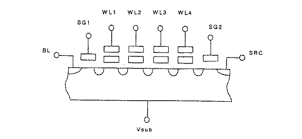
メモリセルMが4個直列接続されたNAND型セルユニットの一端が選択トランジスタSを介してビット線BLに接続され、他端が選択トランジスタSを介して共通ソース線SRCに接続される。メモリセルMの制御ゲート電極はワード線WLに接続され、2つの選択トランジスタSはそれぞれ選択ゲート線SG1,SG2に接続される。
【0065】
1本のワード線WLを共有するメモリセルMはページと言う単位を形成し、4ページで1ブロックを構成する。ここでは、2ブロック分が示されているが、任意の整数、例えば1024ブロックなどでもよい。ビット線BLはBL0〜BL4223の4,224本が示されているが、任意の整数、例えば2112本などでもよい。
【0066】
ビット線制御回路2は、複数のデータ記憶回路10を含む。ここでは、2本のビット線BLに対して1つ設けられているが、任意の整数本、例えば1本や4本や6本や9本などでもよい。
【0067】
カラム選択信号CSLは、カラムデコーダ3の出力信号であり、例えば、ビット線BL0とBL1に接続されるデータ記憶回路10は、カラム選択信号CSL0,CSL1によって選択され、メモリセルのデータはデータ入出力バッファ4に出力される。
【0068】
また、例えば、カラム選択信号CSL2,CLS3によって選択されたビット線BL2,BL3に接続されるデータ記憶回路10には、データ入出力バッファ4から制御データが初期的に転送される。
【0069】
データ記憶回路10は、読み出し時、2本のビット線のうちいずれか一方のビット線に接続されるメモリセルのデータを読み出す。また、データ記憶回路10は、書き込み時も、2本のビット線のうちいずれか一方のビット線に接続されるメモリセルに対し、制御データに従って書き込み制御電圧を印加する。
【0070】
また、データ記憶回路10は、書き込み状態を検出(ベリファイ)する際にも、2本のビット線のうちいずれか一方のビット線に接続されるメモリセルの書き込み状態を検出する。
【0071】
図3は、図2に示されたメモリセルMと選択トランジスタSの構造を示している。
【0072】
p型の半導体基板11(あるいはp型ウェル)の表面にn型の拡散層12が形成され、1方がドレイン、もう1方がソースとなる。
【0073】
メモリセルMでは、半導体基板11(あるいはp型ウェル)上に絶縁膜13を介して浮遊ゲート14が形成され、さらにその上に絶縁膜15を介してワード線WLとなる制御ゲート16が形成される。
【0074】
選択トランジスタSでは、半導体基板11(あるいはp型ウェル)上に絶縁膜17を介して選択ゲート線SGとなる選択ゲート18が形成される。
【0075】
メモリセルMの制御ゲート16にしきい値以上の電圧を印加すると、浮遊ゲート14下にチャネルが形成される。
【0076】
例えば、制御ゲート16と浮遊ゲート14間の容量が1fF、浮遊ゲート14とチャネルの容量が1fF、チャネルと基板11間の容量が0.25fF、n型拡散層12と基板11間の容量が計0.25fFとすると、制御ゲート16とチャネル(またはn型拡散層12)との容量結合比は、50%である。チャネルおよびn型拡散層12が浮遊状態の時、制御ゲート16が1V上昇すると、チャネルあるいはn型拡散層12の電位は、0.5V上昇する。
【0077】
図4は、図2に示されるNAND型セルユニットと2つの選択トランジスタの構造を示している。
【0078】
メモリセルMは、4つが直列接続され、NANDセル列を構成する。NANDセル列の一端は、選択トランジスタSを介して共通ソース線SRCに接続され、その他端は、選択トランジスタSを介してビット線BLに接続される。
【0079】
消去は、基板の電圧Vsubを消去電圧20Vにする。また、選択ゲート線SG1,SG2、ソース線SRC、ビット線BLも20Vにする。消去するブロックのワード線WL1〜WL4を0Vにすると、電子が浮遊ゲートから基板へ放出され、しきい値が負になる(データ“0”の状態)。消去しないブロックのワード線WL1〜WL4を20Vにすると、そのブロックのメモリセルでは、電子が浮遊ゲートから基板へ放出されない。
【0080】
選択されたブロックの選択されたワード線を例えばWL2とすると、書き込み時は、選択されたワード線WL2に書き込み電圧20Vが印加される。選択されたワード線WL2の両隣の非選択ワード線WL1、WL3には、0Vが与えられる。残りの非選択ワード線WL4には11Vが与えられる。
【0081】
また、選択ゲート線SG1には、電源電圧VCCが与えられる。選択ゲート線SG2は0Vである。非選択ブロックの全ワード線WLと全選択ゲート線SGは、0Vである。書き込みを行うメモリセルは、ワード線WL4に繋がるメモリセルからワード線WL1に繋がるメモリセルへ向かって順番に選択される。
【0082】
図4の例では、4つのメモリセルでNAND型メモリセルユニットを構成しているが、例えば、8個や16個のメモリセルから構成してもよい。16個のメモリセルにより1つのユニットを構成する場合、書き込み時に、例えば、ビット線側から4つ目のメモリセルが選択されると、その制御ゲートに繋がるワード線には、書き込み電圧20Vが与えられる。
【0083】
選択されたメモリセルの両隣に存在するビット線側から3番目と5番目のメモリセルの制御ゲートに繋がる2本のワード線には、0Vが与えられる。残りの13個のメモリセルの制御ゲートに繋がる13本のワード線には、11Vが与えられる。
【0084】
また、書き込み時に、ビット線側から2つ目のメモリセルが選択されると、その制御ゲートに繋がるワード線に書き込み電圧20Vが与えられる。選択されたメモリセルの両隣に存在するビット線側から1番目と3番目のメモリセルの制御ゲートに繋がる2本のワード線には、0Vが与えられる。残りの13個のメモリセルの制御ゲートに繋がる13本のワード線には、11Vが与えられる。
【0085】
また、書き込み時に、ビット線側から1つ目のメモリセルが選択されると、その制御ゲートに繋がるワード線に書き込み電圧20Vが与えられる。選択されたメモリセルの隣に存在するビット線側から2番目のメモリセルの制御ゲートに繋がるワード線には、0Vが与えられる。残りの14個のメモリセルの制御ゲートに繋がる14本のワード線には、11Vが与えられる。
【0086】
書き込みは、選択ブロックについてメモリセルのデータの一括消去を行い、各メモリセルがデータ“0”を記憶している状態に揃えた後に例えばページ単位で行われる。
【0087】
例えば、4値記憶の場合、データ“1”、“2”、“3”を書き込むときは、ビット線BLを0Vの書き込み制御電圧にする。メモリセルは、ワード線WL4に繋がるものからワード線WL1に繋がるものへ順番に選択されるため、選択されたメモリセルよりもビット線側に存在するメモリセルは、常に消去状態にあることになる。
【0088】
よって、選択されたメモリセルよりもビット線側に存在するメモリセルのワード線が0Vに設定されていても、ビット線の書き込み制御電圧(0V)は、選択されたメモリセルに転送される。
【0089】
これによって、選択メモリセルでは、基板から浮遊ゲートへ電子が移動し、選択メモリセルのしきい値が正になる。
【0090】
また、データ“0”を書き込む場合は、ビット線BLを電源電圧VCCの書き込み制御電圧にする。選択ゲートSG1が電源電圧VCCであるため、“0”書き込み時はビット線側の選択ゲートSが非導通になり、各メモリセルのチャネルとn型拡散層12は浮遊状態となる。
【0091】
その結果、ワード線に書き込み電圧20Vが与えられた選択メモリセルのチャネルの電位及びワード線に11Vが与えられた非選択メモリセルのチャネルの電位は、それぞれ上昇する。そして、選択されたメモリセルの両隣に存在するメモリセルは、ワード線に0Vが与えられているため、チャネルの電位が所定値になると、非導通となる。
【0092】
選択されたメモリセルのチャネル電位は、容量結合比が50%の場合、書き込み電圧20Vによって約10Vまで上昇する。この場合、選択されたメモリセルの制御ゲートとチャネルの電位差が小さいため、選択メモリセルの浮遊ゲートには電子が注入されず、データ“0”書き込みが行える。
【0093】
但し、選択されたメモリセルの両隣のメモリセルのしきい値が過度に負の方に深いと、書き込み時に、その制御ゲートに0Vを与えても非導通にならない。このため、後に詳しく説明するように、メモリセルのデータを一括消去(選択ブロックのみ)した後、いわゆる事前書き込みを行って、各メモリセルのしきい値を制御している。
【0094】
また、データ“1”、“2”、“3”を書くときのビット線BLの書き込み制御電圧は0Vであるが、後に詳しく説明するように、その0Vの書き込み制御電圧が印加される時間をデータに応じて調整する。
【0095】
例えば、データ“1”書き込み時は、データ、“2”、“3”書き込み時よりも0Vの書き込み制御電圧がビット線に印加される時間を短くする。これは、データ“1”を記憶させるためにメモリセルMの浮遊ゲートに注入する電子量は、データ、“2”、“3”を記憶させるために注入する電子より少なくてよいためである。
【0096】
さらに、データ“1”、“2”、“3”をそれぞれ書き込むために、書き込みデータに応じてビット線に0Vの書き込み制御電圧を印加する時間を異ならしめてもよい。具体的には、データ“1”、“2”、“3”書き込みのための書き込み制御電圧の印加時間は、それぞれ1μsec、5μsec、25μsecとなる。
【0097】
例えば、4値記憶の場合、データ“0”に対応するメモリセルのしきい値は、0V以下に、データ“1”に対応するメモリセルのしきい値は、0.3V〜0.7Vの範囲に、データ“2”に対応するメモリセルのしきい値は、1.5V〜1.9Vの範囲に、データ“3”に対応するメモリセルのしきい値は、2.7V〜3.1Vの範囲に設定される。
【0098】
読み出し時は、例えば、ワード線WL2に繋がるメモリセルが選択されているとすると、選択されたブロックの選択ワード線WL2をVcgにする。選択されたブロックの非選択ワード線WL1、WL3とWL4は、例えば、Vread=4.5Vにする。選択されたブロックの選択ゲート線SG1とSG2も、Vread=4.5Vにする。非選択ブロックの全ワード線WL及び選択ゲート線SG1は、0Vである。ソース線SRCは、寄生抵抗を介して0Vに接地される。
【0099】
共通ソース線の電位が寄生抵抗によって上昇しなければ、
(1) Vcgを0Vにして、選択メモリセルがデータ“1”か“2”か“3”を記憶していれば、1Vに充電された浮遊状態のビット線の電圧は、1Vのままである。一方、選択メモリセルがデータ“0”を記憶していれば、1Vに充電された浮遊状態のビット線の電圧は、0.5Vに下がる。
【0100】
(2) Vcgを1.1Vにして、選択メモリセルがデータ“2”か“3”を記憶していれば、1Vに充電された浮遊状態のビット線の電圧は、1Vのままである。選択メモリセルがデータ“0”か“1”を記憶していれば、1Vに充電された浮遊状態のビット線の電圧は、0.5Vに下がる。
【0101】
(3) Vcgを2.3Vにして、選択メモリセルがデータ“3”を記憶していれば、1Vに充電された浮遊状態のビット線の電圧は、1Vのままである。選択メモリセルがデータ“0”か“1”か“2”を記憶していれば、1Vに充電された浮遊状態のビット線の電圧は、0.5Vに下がる。
【0102】
以上の(1)〜(3)より、メモリセルMに記憶されているデータを判定することができる。
【0103】
図5は、図2のデータ記憶回路10の具体的な構成例を示している。
【0104】
クロック同期式インバータCI1,CI2及びnチャネルMOSトランジスタQn3,Qn4,Qn5で第1のサブデータ回路を構成する。また、クロック同期式インバータCI3,CI4及びnチャネルMOSトランジスタのQn10,Qn11,Qn12で第2のサブデータ回路を構成する。
【0105】
第1及び第2のサブデータ回路は、それぞれ書き込み時に、第1及び第2のサブデータを記憶する。第1及び第2のサブデータ回路は、それぞれ読み出し時に、第1及び第2の読み出しサブデータを記憶する。
【0106】
第1のサブデータ回路内のノードNaiが“H”レベルである状態は、第1のサブデータ回路が“1”の第1の読み出しサブデータあるいは“1”の第1のサブデータを記憶している状態である。また、第2のサブデータ回路内のノードNai+1が“H”レベルである状態は、第2のサブデータ回路が“1”の第2の読み出しサブデータあるいは“1”の第2のサブデータを記憶している状態である。
【0107】
第1のサブデータ回路内のノードNaiが“L”レベルの状態は、第1のサブデータ回路が“0”の第1の読み出しサブデータあるいは“0”の第1のサブデータを記憶している状態である。第2のサブデータ回路内のノードNai+1が“L”レベルの状態は、第2のサブデータ回路が“0”の第2の読み出しサブデータあるいは“0”の第2のサブデータを記憶している状態である。
【0108】
pチャネルMOSトランジスタQp1及びQp2は、信号PRSTB1及びPRSTB2が“L”となって第1及び第2のサブデータ回路に“0”のサブデータを設定するものである。
【0109】
nチャネルMOSトランジスタQn1,Qn8は、第1及び第2のサブデータ回路とそれぞれ入出力線IOL、IOUを電気的に接続するためのものである。それぞれのゲート電極には、カラムデコーダ3からの出力CSLi及びCSLi+1がそれぞれ与えられる。
【0110】
例えば、CSLiが“H”になると、ビット線BLiとBLi+1に設けられたデータ記憶回路10の第1のサブデータ回路とデータ入出力線IOLが電気的に接続される。データ入出力線IOL、IOUは、データ入出力バッファ4に接続されていて、この第1あるいは第2のサブデータ回路にサブデータを設定することができる。あるいは、この第1あるいは第2のサブデータ回路の読み出しサブデータをデータ入出力バッファ4に出力することができる。
【0111】
nチャネルMOSトランジスタQn2及びQn9は、第1のサブデータ回路及び第2のサブデータ回路のサブデータが全て“0”か否かを検出する。データ記憶回路10は、この例では2112個あるので、2112個の第1のサブデータと2112個の第2のサブデータが全て“0”であれば、共通信号線PTと接地線が非導通となって検出される。
【0112】
nチャネルMOSトランジスタQn6,Qn7は、第1のサブデータ回路に記憶されているサブデータに応じて、ビット線BLの電圧を下げるためのものである。また、nチャネルMOSトランジスタQn13,Qn14は、第2のサブデータ回路に記憶されているサブデータに応じて、ビット線BLの電圧を下げるためのものである。nチャネルMOSトランジスタQn15は、ビット線BLを充電するためのものである。
【0113】
nチャネルMOSトランジスタQn16,Qn18は、第1及び第2のサブデータ回路とビット線BLiあるいはBLi+1の電気的接続を制御する。信号BLC1が“H”でBLC2が“L”であれば、第1及び第2のサブデータ回路とビット線BLiが電気的に接続される。
【0114】
信号BLC1が“L”でBLC2が“H”であれば、第1及び第2のサブデータ回路とビット線BLi+1が電気的に接続される。nチャネルMOSトランジスタQn17及びQn19は、ビット線BLiと電圧VBL1の電気的接続、ビット線BLi+1と電圧BL2の電気的接続を制御する。
【0115】
信号PRE1が“H”であれば、ビット線BLiと電圧VBL1が電気的に接続される。信号PRE2が“H”であれば、ビット線BLi+1と電圧VBL2が電気的に接続される。
【0116】
ビット線BLiあるいはビット線BLi+1を介してメモリセルMのデータあるいは書き込み状態を示す信号が転送される。第1のサブデータ回路ではクロック同期式インバータCI1が、第2のサブデータ回路ではクロック同期式インバータCI3が、ビット線BLの信号の論理レベルをセンスするセンスアンプとしても働く。
【0117】
クロック同期式インバータCIの具体的な構成は、図6に示されている。
【0118】
nチャネルMOSトランジスタQn20とpチャネルMOSトランジスタQp4で構成されるインバータ回路の入力端子がINで出力端子OUTである。このインバータ回路を信号CLOCKとその反転信号CLOCKBによって活性化したり非活性化するためnチャネルMOSトランジスタQn21とpチャネルMOSトランジスタQp3が設けられている。信号CLOCKが“H”、CLOCKBが“L”で活性化され、信号CLOCKが“L”、CLOCKBが“H”で非活性化される。
【0119】
信号SEN1、LAT1、SEN2、LAT2、PRO1、PRO2、BLC1、BLC2、PRE1、PRE2、VRFY1、VRFY2、VRFY3、PRO10、PRSTB1、PRSTB2、BIAS、VBL1、VBL2、VREGは、制御信号及び制御電圧発生回路7の出力信号で、図2にみられるデータ記憶回路10の全てに共通である。信号PTも制御信号及び制御電圧発生回路7に入力される。電圧VCCは電源電圧で例えば3Vである。
【0120】
第1及び第2のサブデータ回路は、“0”あるいは“1”のサブデータを記憶し、各々、ビット線信号の“H”レベルに応答して記憶されている“1”のサブデータを“0”のサブデータに変更し、“0”のサブデータを保持するよう構成されている。
【0121】
図5の回路の動作を説明する。信号PRO1あるいはPRO2が“H”となってビット線BLの電圧レベルがクロック同期式インバータCI1あるいはCI3でセンスされる前に、第1あるいは第2のサブデータに応じて、ビット線BLの電圧レベルがnチャネルMOSトランジスタQn4、5あるいはQn11、12によって調整される。
【0122】
第1あるいは第2のサブデータが“0”の場合のみ、ビット線BLの電圧レベルは“H”にされる。信号PRO1あるいはPRO2が“H”となって、このときビット線の“H”レベルがクロック同期式インバータCI1あるいはCI3の入力端子に転送されると、ノードNaiあるいはNai+1が“L”レベルにされる。
【0123】
さらに、クロック同期式インバータCI2あるいはCI4によって、“0”のサブデータが記憶される。よって、もともと記憶されている“0”のサブデータは変更されない。もともと記憶されているサブデータが“1”の場合は、ビット線BLのレベルが“H”の時“0”のサブデータに変更され記憶され、ビット線BLのレベルが“L”の時“1”のサブデータを保持する。
【0124】
なお、データ記憶回路10の具体的な構成は図5に示した例に限定されず、種々様々な構成により実現できる。
【0125】
図7は、ワード線制御回路6の具体的な構成の一例を示している。なお、図2に示されるブロックごとに、図7に示される回路が設けられることになる。
【0126】
信号Pi(i=0〜Np)、Qi(i=0〜Nq)、Ri(i=0〜Nr)は、ブロックアドレス信号である。Piのうち選択された1つだけがVCCとなる。Qiのうち選択された1つだけがVCCとなる。Riのうち選択された1つだけがVCCとなる。Np=7、Nq=7、Nr=15で、Np×Nq×Nr=1024ブロックが選択可能である。
【0127】
ブロックに対応する信号Pi、Qi、Riの組み合わせが全て“H”になると、そのブロックは選択される。信号Piは、nチャネルMOSトランジスタQn25とpチャネルMOSトランジスタQp5に入力される。信号Qiは、nチャネルMOSトランジスタQn26とpチャネルMOSトランジスタQp6に入力される。
【0128】
信号Riは、nチャネルMOSトランジスタQn27とpチャネルMOSトランジスタQp7に入力される。信号Pi、Qi、Riの組み合わせが全て“H”になると、インバータI2の入力が“L”となってこのブロックは選択される。このブロックが不良の場合、フューズF1は切断される。
【0129】
フューズF1が切断されると、信号Pi、Qi、Riの組み合わせが全て“H”になっても、インバータI2の入力は“H”のままである。インバータI2とpチャネルMOSトランジスタQp8で、インバータI2の入力は“H”に固定されている。
【0130】
このブロックが選択されると、ディプレッションタイプnチャネルMOSトランジスタQnd1を介して、nチャネルMOSトランジスタQn28〜Qn31のゲートが“H”になる。また、信号SGD1、WLD1〜4、SGD2がそれぞれ選択ゲート線SG1、ワード線WL1〜WL4、選択ゲート線SG2に転送される。
【0131】
このブロックが選択されてない場合、信号WLGNDBが“L”であれば、NOR論理回路G2の出力が“H”となり、nチャネルMOSトランジスタQn32〜Qn34が導通して、選択ゲート線SG1とワード線WL1〜WL4は接地される。
【0132】
nチャネルMOSトランジスタQn22〜24、キャパシタC1、C2、インバータI1、NAND論理回路G1は、電源電圧VCCより高い電圧VPPRWを、選択されたブロックのnチャネルMOSトランジスタQn28〜Qn31のゲートに転送するための回路である。
【0133】
信号OSCは、一定の周期で“L”と“H”となる信号である。電圧VPPRWを転送する場合、信号BWLHBを0Vにする。なぜなら、ディプレッションタイプnチャネルMOSトランジスタQnd1は、そのゲートが電源電圧VCCのとき、ドレインからソースへ電源電圧VCCを転送できるようにされていて、そのゲートが0Vのとき、ドレインからソースへ電源電圧VCCを転送できないようにされているからである。
【0134】
信号OSC、BWLHB、WLGNDB、SGD1、WLD1〜4、SGD2、VPPRWは、制御信号及び制御電圧発生回路7の出力信号で、各ブロックのワード線制御回路6全てに共通である。
【0135】
図8は、メモリセルに記憶されている4値データの読み出し動作を示す。
【0136】
ここでは、ビット線BL0、BL2、…、BLi、…、BL4222が選択され(代表としてBLiを示す)、ワード線WL2が選択されている場合を示す。また、信号VBL1,VBL2の電圧は0V、信号BLC2の電圧は0V、信号PRE2の電圧はVCC、ビット線BLi+1の電圧は0V、信号VRFY1の電圧は0V、信号VRFY3の電圧は0V、信号PRO10の電圧は0V、信号CSLi,CSLi+1の電圧は0V、信号VREGの電圧は0Vのままなので、図8への表示を省略している。
【0137】
まず、選択されたブロックの選択ゲート線SG1が4.5Vになる。同時に、信号PRE1がVCCから0V、BLC1が0Vから7Vとなってビット線BLiが選択される。信号BIASが0Vから1.8Vとなってビット線BLiが0.8Vに充電される。
【0138】
nチャネルMOSトランジスタQnのしきい値は、断らない限り1Vとする。信号BIASが0Vとなってビット線BLiの充電は終了する。続いて、選択されたブロックの選択ゲート線SG2及び非選択ワード線WL1、WL3、WL4が0Vから4.5Vにされ、選択ワード線WL2が0Vから2.3Vにされる。
【0139】
なお、表1は、メモリセルMに記憶されているデータと、そのメモリセルのしきい値の関係を示している。
【0140】
【表1】
選択ワード線WL2が2.3Vになると、メモリセルが“3”データを記憶している場合のみビット線BLiは、0.8Vのままである。それ以外の場合は、ビット線BLiは、0.5V以下となる。一定期間経った後、選択ゲート線SG2及び非選択ワード線WL1〜WL4が0.0Vにされる。
【0142】
選択ゲート線SG2が0Vにリセットされた後、信号SEN2、LAT2をVCCから0Vにする。信号PRSTB2をVCCから0Vにすると、ノードNbi+1がVCCとなる。信号PRSTB2をVCCに戻した後、信号PRO2を0Vから1.6Vにする。
【0143】
メモリセルが“3”データを記憶している場合、ビット線BLiは0.8Vをを維持しているので、nチャネルMOSトランジスタQn10は、非導通で、ノードNbi+1は、VCCを維持する。
【0144】
メモリセルが“3”以外のデータを記憶している場合、ビット線BLiは、0.5V以下で、nチャネルMOSトランジスタQn10は、導通し、ノードNbi+1の電位は、電源電圧VCCから下がる。
【0145】
例えば、1本のビット線BLの容量が5pFで、ノードNbi+1の寄生容量が0.1pFとすると、VCC=3Vのとき、ノードNbi+1は、約0.55V以下に下がる。
【0146】
信号SEN2がVCCに戻りクロック同期式インバータCI3が活性化され、ノードNbi+1の電圧がセンスされる。信号LAT2がVCCに戻ると、クロック同期式インバータCI4が活性化され、センスされた信号の論理レベルが第2のサブデータ回路にラッチされる。
【0147】
再び、信号PRO2が0Vとなって、ビット線BLiとノードNbi+1が切り離された後、信号PRE1がVCCに戻って、ビット線BLiは、0Vにリセットされ、メモリセルMのしきい値が2.3V以上かどうかを検出する動作が終わる。
【0148】
メモリセルが“3”データを記憶している場合のみ、第2のサブデータ回路の第2の読み出しサブデータは“0”となる。それ以外の場合は、第2の読み出しサブデータは“1”である。
【0149】
次に、メモリセルMのしきい値が0.0V以上かどうかを検出する動作に入る。信号PRE1がVCCから0Vにされ、信号BIASが0Vから1.8Vとなってビット線BLiが0.8Vに充電される。信号BIASが0Vとなってビット線BLiの充電は終了する。
【0150】
続いて、選択されたブロックの選択ゲート線SG2及び非選択ワード線WL1,WL3,WL4が、0Vから4.5Vにされる。同時に、信号VRFY2が0VからVCCにされ、第2のサブデータ回路の読み出しサブデータが“0”の場合(すなわちメモリセルMが“3”のデータを記憶しているとき)、nチャネルMOSトランジスタQn12が導通し、ビット線BLiの電位は0Vに下がる。
【0151】
選択ワード線WL2が0.0Vのままなので、メモリセルが“1”あるいは“2”のデータを記憶している場合は、ビット線BLiは、0.8Vのままである。メモリセルが“0”あるいは“3”のデータを記憶している場合は、ビット線BLiは、0.5V以下となる。
【0152】
一定期間経った後、選択ゲート線SG2及び非選択ワード線WL1,WL3,WL4が0.0Vにされる。また、信号VRFY2も、0Vに戻される。
【0153】
選択ゲート線SG2が0Vにリセットされた後、信号SEN1、LAT1をVCCから0Vにする。信号PRSTB1をVCCから0Vにすると、ノードNbiがVCCとなる。信号PRSTB1をVCCに戻した後、信号PRO1が0Vから1.6Vにする。
【0154】
メモリセルが“1”あるいは“2”データを記憶している場合、ビット線BLiは、0.8Vを維持しているので、nチャネルMOSトランジスタQn3は非導通で、ノードNbiはVCCを維持する。
【0155】
メモリセルが“0”あるいは“3”のデータを記憶している場合、ビット線BLiは、0.5V以下で、nチャネルMOSトランジスタQn3は、導通し、ノードNbiの電位は、電源電圧VCCから下がる。
【0156】
例えば、1本のビット線BLの容量が5pFで、ノードNbiの寄生容量が0.1pFとすると、VCC=3Vのとき、ノードNbiは、約0.55V以下に下がる。
【0157】
信号SEN1がVCCに戻りクロック同期式インバータCI1が活性化され、ノードNbiの電圧がセンスされる。信号LAT1がVCCに戻るとクロック同期式インバータCI2が活性化され、センスされた信号の論理レベルが第1のサブデータ回路にラッチされる。
【0158】
再び、信号PRO1が0Vとなってビット線BLiとNbiが切り離された後、信号PRE1がVCCに戻って、ビット線BLiは0Vにリセットされ、メモリセルMのしきい値が0.0V以上かどうかを検出する動作が終わる。
【0159】
メモリセルが“1”あるいは“2”データを記憶している場合、第1のサブデータ回路の第1の読み出しサブデータは“0”となる。メモリセルが“0”あるいは“3”データを記憶している場合は、第1の読み出しサブデータは“1”である。
【0160】
次に、メモリセルMのしきい値が1.1V以上かどうかを検出する動作に入る。信号PRE1がVCCから0Vにされ、信号BIASが0Vから1.8Vとなってビット線BLiが0.8Vに充電される。信号BIASが0Vとなってビット線BLiの充電は終了する。
【0161】
続いて、選択されたブロックの選択ゲート線SG2及び非選択ワード線WL1,WL3,WL4が0Vから4.5Vにされ、選択ワード線WL2が0Vから1.1Vにされる。
【0162】
選択ワード線WL2が1.1Vになると、メモリセルが“2”あるいは“3”データを記憶している場合、ビット線BLiは0.8Vのままである。メモリセルが“0”あるいは“1”データを記憶している場合、ビット線BLiは0.5V以下となる。一定期間経った後、選択ゲート線SG2及び非選択ワード線WL1〜WL4が0.0Vにされる。
【0163】
選択ゲート線SG2が0Vにリセットされた後、信号SEN2、LAT2をVCCから0Vにすると、信号PRSTB2をVCCから0Vにすると、ノードNbi+1がVCCとなる。信号PRSTB2をVCCに戻した後、信号PRO2を0Vから1.6Vにする。
【0164】
メモリセルが“2”あるいは“3”データを記憶している場合、ビット線BLiは0.8Vを維持しているので、nチャネルMOSトランジスタQn10は、非導通で、ノードNbi+1は、VCCを維持する。
【0165】
メモリセルが“0”あるいは“1”のデータを記憶している場合、ビット線BLiは、0.5V以下で、nチャネルMOSトランジスタQn10は、導通し、ノードNbi+1の電位は、VCCから約0.55V以下に下がる。信号SEN2がVCCに戻りクロック同期式インバータCI3が活性化され、ノードNbi+1の電圧がセンスされる。
【0166】
信号LAT2がVCCに戻るとクロック同期式インバータCI4が活性化され、センスされた信号の論理レベルが第2のサブデータ回路にラッチされる。再び、信号PRO2が0Vとなってビット線BLiとNbi+1が切り離された後、信号PRE1がVCCに戻って、ビット線BLiは0Vにリセットされ、メモリセルMのしきい値が1.1V以上かどうかを検出する動作が終わる。
【0167】
メモリセルが“2”あるいは“3”データを記憶している場合、第2のサブデータ回路の第2の読み出しデータは“0”となる。メモリセルが“0”あるいは“1”データを記憶している場合、第2の読み出しサブデータは“1”である。最後に、選択ゲート線SG1が0Vに、信号BLC1が0Vに戻り、読み出し動作が終了する。
【0168】
このように図8に示すように、メモリセルMのデータが読み出しデータとしてデータ記憶回路10へ記憶される動作が終わる。この後、信号CSLi、CSLi+1が0VからVCCになると、第1の読み出しサブデータは、データ入出力線IOLに出力され、第2の読み出しサブデータは、データ入出力線IOUに出力され、これらのデータは、データ出力バッファ4を介してデータ入出力端子5からLSI外部へ出力される。
【0169】
表2は、メモリセルの4値データと第1及び第2の読み出しサブデータの関係を示している。
【0170】
【表2】
図9は、図8に示した読み出し時におけるワード線制御回路6の動作を示す。
【0172】
選択されたブロックアドレス信号Pi、Qi、Riが0VからVCCとなって、信号BWLHBがVCCから0Vに、信号VPPRWがVCCから4.5Vとなり、信号OSCが0VとVCCの間で振動し始めると、選択されたブロックのnチャネルMOSトランジスタQn28〜Qn31のゲートが5.5Vになる。
【0173】
nチャネルMOSトランジスタQn28〜Qn31のゲートの電圧は、信号VPPRWにnチャネルMOSトランジスタQn24のしきい値を加えたものになる。また、信号WLGNDBは0Vのままなので、選択されたブロックのnチャネルMOSトランジスタQn32〜Qn34のゲートは0Vで非導通である。
【0174】
逆に、非選択ブロックのnチャネルMOSトランジスタQn28〜Qn31のゲートの電圧は0Vで、非導通である。また、非選択されたブロックのnチャネルMOSトランジスタQn32〜Qn34のゲートはVCCで導通する。
【0175】
信号SGD1がVCCから4.5Vに、WLD2が0Vから2.3Vに、WLD1,WLD3,WLD4が0Vから4.5Vに、SGD2が0Vから4.5Vになって、選択されたブロックの選択ゲート線SG1が0Vから4.5Vに、ワード線WL2が0Vから2.3Vに、ワード線WL1、WL3、WL4が0Vから4.5Vに、SG2が0Vから4.5Vになる。
【0176】
一定期間経った後、信号WLD2が2.3Vから0Vに、信号WLD1,WLD3,WLD4が4.5Vから0Vに、SGD2が4.5Vから0Vになって、選択されたブロックのワード線WL2が2.3Vから0Vに、ワード線WL1,WL3,WL4が4.5Vから0に、SG2が4.5Vから0Vにりセットされる。
【0177】
同様に、信号WLD1,WLD3,WLD4が0Vから4.5Vに、SGD2が0Vから4.5Vになって、選択されたブロックのワード線WL1,WL3,WL4が0Vから4.5Vに、SG2が0Vから4.5Vになる。
【0178】
一定期間経った後、信号WLD1,WLD3,WLD4が4.5Vから0Vに、SGD2が4.5Vから0Vになって、選択されたブロックのワード線WL1,WL3,WL4が4.5Vから0に、SG2が4.5Vから0Vにリセットされる。
【0179】
再度、同様に、信号WLD2が0Vから1.1Vに、信号WLD1,WLD3,WLD4が0Vから4.5Vに、SGD2が0Vから4.5Vになって、選択されたブロックのワード線WL2が0Vから1.1Vに、ワード線WL1,WL3,WL4が0Vから4.5Vに、SG2が0Vから4.5Vになる。
【0180】
一定期間経った後、信号WLD2が1.1Vから0Vに、信号WLD1,WLD3,WLD4が4.5Vから0Vに、SGD2が4.5Vから0Vになって、選択されたブロックのワード線WL2が1.1Vから0Vに、ワード線WL1,WL3,WL4が4.5Vから0に、SG2が4.5Vから0Vにリセットされる。
【0181】
非選択ブロックの選択ゲート線SG1とワード線WL1〜WL4は、nチャネルMOSトランジスタQn32〜Qn34によって0Vである。選択されたブロックアドレス信号Pi、Qi、PiがVCCから0Vとなって、信号BWLHBが0VからVCCに、信号VPPRWが4.5VからVCCとなり、信号OSCが0Vとなって、選択されたブロックのnチャネルMOSトランジスタQn28〜Qn31のゲートは、0Vにリセットされる。
【0182】
また、選択されたブロックのnチャネルMOSトランジスタQn32〜Qn34のゲートは、VCCにもどされ、導通する。これで非選択状態に戻り、選択ゲート線SG1が0Vに戻る。
【0183】
図10は、書き込み(ページ書き込み)動作を示している。
【0184】
ここでは、ビット線BL0、BL2、…、BLi、…、BL4222が選択され(代表としてBLiを示す)、ワード線WL2が選択されている場合を示す。
【0185】
書き込みに先だって、データ記憶回路10への制御データの初期設定が行われる。ビット線BLiに備えられたデータ記憶回路10への制御データの初期設定は次のように行われる。
【0186】
第1のサブデータ回路の初期サブデータが入出力線IOL、第2のサブデータ回路の初期サブデータが入出力線IOUに転送され、信号CSLiとCSLi+1が0VからVCCになって、第1及び第2のサブデータ回路に初期サブデータが記憶される。信号CSLの選択を変えて、任意の数の任意データ記憶回路10に初期制御データは設定される。
【0187】
このとき、初期制御データと初期サブデータの関係は、以下の表3に示すようになる。
【0188】
【表3】
ここで、全ての初期制御データ設定以前に、信号PRSTB1とPRSTB2をVCCから0Vにし、再度VCCに戻して、全てのデータ記憶回路10の制御データを“0”にリセットしておくことが望ましい。
【0190】
後で説明するように、制御データ“0”によってメモリセルMの状態は変化させられないので、2112個のデータ記憶回路10の内、所望のデータ記憶回路10のみに外部から初期制御データを設定すればよい。もちろん2112個全部のデータ記憶回路10の初期制御データを外部から設定してもよい。
【0191】
信号BLC2は0V、BIASは0V、VRFY1〜3は0V、PRO1は0V、SEN1はVCC、LAT1はVCC、SEN2はVCC、LAT2はVCC、PRSTB1とPRSTB2はVCC、CSLiとCSLi+1は0V、信号VBL1とVREGは0Vのままなので図10への表示は省略してある。
【0192】
書き込み動作では、先ず、選択されたブロックの選択ゲート線SG1がVCCになる。同時に、信号PRE1がVCCから0V、BLC1が0Vから7Vとなってビット線BLiが選択される。信号PRO2が7Vとなって、第2のサブデータが“0”の場合、ビット線BLiはVCCの書き込み制御電圧にされる。
【0193】
第2のサブデータが“1”の場合、ビット線BLiは0Vのままで、0Vの書き込み制御電圧にされる。信号PRE2がVCCから7Vとなり、信号VBL2が0VからVCCになって、非選択のビット線BLi+1はVCCの書き込み制御電圧にされる。共通ソース線SRCもVCCにされる。これは、選択されたブロックの選択ゲート線SG2のパンチスル−を防ぐためである。
【0194】
その後、選択されたブロックのワード線WL2が書き込み電圧Vpgm(16V〜20V)となる。両隣のワード線WL1,WL3は0Vである。残りのワード線WL4は11Vにされる。これで、“2”あるいは“3”の制御データを記憶しているデータ記憶回路10に対応するメモリセルMでは、そのしきい値が上昇していく。“0”あるいは“1”の制御データを記憶しているデータ記憶回路10に対応するメモリセルMでは、その状態は保持される。非選択ビット線BLi+1に繋がるメモリセルMの状態も保持される。
【0195】
例えば、8μsec後に選択されたワード線WL2がVpgmから0Vに、ワード線WL4が11Vから0Vにリセットされる。同時に、信号PRO2が7Vから0Vにリセットされる。
【0196】
この時点では、ビット線上の書き込み制御電圧は変化しない。信号PRO10が0VからVCCとなって、第1のサブデータ回路のサブデータが“1”の場合、ビット線BLiは0Vの書き込み制御電圧となる。この時点で、ビット線BLiの書き込み制御電圧は、対応するデータ記憶回路10に記憶されている制御データが“0”の場合にVCC、制御データが“1”あるいは“2”あるいは“3”の場合に0Vである。
【0197】
再度、選択されたブロックのワード線WL2が書き込み電圧Vpgm(16V〜20V)となり、ワード線WL4は11Vにされる。
【0198】
例えば、2μsec後に、再度、選択されたワード線WL2がVpgmから0Vに、ワード線WL4が11Vから0Vにリセットされる。その後、信号PRO10はVCCから0Vに、BLC1は7Vから0Vに、PRE1は0VからVCCにリセットされ、ビット線BLiは0Vにリセットされる。
【0199】
また、信号VBL2がVCCから0Vとなって、ビット線BLi+1も0Vにリセットされる。信号PRE2は7VからVCCに、共通ソース線SRCはVCCから0Vに、選択ゲート線SG1はVCCから0Vにリセットされて、書き込みが終了する。
【0200】
書き込み後、データがメモリセルに書き込めているか否かを確認する書き込みベリファイが後述のように行われる。全ての選択されたメモリセルに書き込めていると確認されるまで、書き込みと書き込みベリファイは繰り返される。
【0201】
図10に示したように、“1”書き込み時のビット線上に0Vの書き込み制御電圧が与えられている時間は、“2”あるいは“3”書き込み時のビット線上に0Vの書き込み制御電圧が与えられている時間より短くされる。これによって、例えば、メモリセルに“1”を書き込むのに必要な書き込み回数と、“2”を書き込むのに必要な回数をほぼ等しくできる。1回の書き込み動作でメモリセルの浮遊ゲートに注入される電荷量が、“1”、“2”、“3”の順に少ないからである。
【0202】
例えば、一定の書き込み電圧を制御ゲートに印加して、ソースとドレインを0Vに固定する。メモリセルのしきい値の変化分ΔVtは書き込み時間をtpとすると、
ΔVt log(tp)
なので、書き込み時間をα倍にしたメモリセルとのしきい値差DVtは、
DVt log(α×tp)−log(tp)=log(α)
となり、常に一定である。
【0203】
“1”書き込み状態にメモリセルが到達するまでの書き込み動作回数と、“2”書き込み状態にメモリセルが到達するまでの書き込み動作回数は、“1”書き込み時の一回の書き込み時間を“2”書き込み時の一回の書き込み時間より短くすることで、等しくできる。書き込み動作回数が等しければ、“1”書き込み終了時点で、“2”書き込みも同時に終了する。
【0204】
もし、1回の書き込み動作で注入される電荷量が等しいと、“1”書き込みが終了した時点で“2”書き込みや“3”書き込みはまだ終わってない。よって、複数のNAND型セルユニットに対して同時に書き込む場合は、書き込み時間が長くなる。
【0205】
図11は、図10に示した書き込み時におけるワード線制御回路6の動作を示す。
【0206】
選択されたブロックアドレス信号Pi、Qi、Riが0VからVCCとなって、信号BWLHBがVCCから0Vに、信号VPPRWがVCCからVpgmとなり、信号OSCが0VとVCCの間で振動し始めると、選択されたブロックのnチャネルMOSトランジスタQn28〜Qn31のゲートがVpgm+1Vになる。
【0207】
nチャネルMOSトランジスタQn28〜Qn31のゲートの電圧は、信号VPPRWにnチャネルMOSトランジスタQn24のしきい値を加えたものになる。また、信号WLGNDBは0Vのままなので、選択されたブロックのnチャネルMOSトランジスタQn32〜Qn34のゲートは0Vで非導通である。
【0208】
よって、選択ブロックの選択ゲート線SG1はVCCとなる。逆に、非選択ブロックのnチャネルMOSトランジスタQn28〜Qn31のゲートの電圧は0Vで、非導通である。また、非選択されたブロックのnチャネルMOSトランジスタQn32〜Qn34のゲートはVCCで導通する。
【0209】
信号WLD2が0VからVpgmに、WLD4が0Vから11Vになって、選択されたブロックのワード線WL2が0VからVpgmに、WL4が0Vから11Vになる。
【0210】
続いて、信号WLD2がVpgmから0Vに、WLD4が11Vから0Vになって、選択されたブロックのワード線WL2がVpgmから0Vに、WL4が11Vから0にリセットされる。
【0211】
再度、信号WLD2が0VからVpgmに、WLD2が0Vから11Vになって、選択されたブロックのワード線WL2が0VからVpgmに、WL4が0Vから11Vになる。
【0212】
続いて、信号WLD2がVpgmから0Vに、WLD4が11Vから0Vになって、選択されたブロックのワード線WL2がVpgmから0Vに、WL4が11Vから0にリセットされる。
【0213】
非選択ブロックの選択ゲート線SG1とワード線WL1〜WL4はnチャネルMOSトランジスタQn32〜Qn34によって0Vである。選択されたブロックアドレス信号Pi、Qi、RiがVCCから0Vとなって、信号BWLHBが0VからVCCに、信号VPPRWがVpgmからVCCとなり、信号OSCが0Vとなって、選択されたブロックのnチャネルMOSトランジスタQn28〜Qn31のゲートは0Vにリセットされる。
【0214】
また、選択されたブロックのnチャネルMOSトランジスタQn32〜Qn34のゲートはVCCにもどされ、導通する。これで非選択状態に戻り、選択ゲート線SG1が0Vに戻る。
【0215】
図12は、図10あるいは図11の書き込み動作後におけるメモリセルの書き込み状態を検出する書き込みベリファイ動作を示す。
【0216】
ここでは、ビット線BL0、BL2、…、BLi、…、BL4222が選択され(代表としてBLiを示す)、ワード線WL2が選択されている場合を示す。また、ここでは、信号VBL1、VBL2は0V、信号BLC2は0V、PRE2はVCCのままで、ビット線BLi+1が0Vのままなので、図12への表示を省略している。また、信号PRO10が0V、CSLiが0V、CSLi+1が0Vのままなので、図12への表示を省略している。
【0217】
まず、選択されたブロックの選択ゲート線SG1が4.5Vになる。同時に、信号PRE1がVCCから0V、BLC1が0Vから7Vとなってビット線BLiが選択される。信号BIASが0Vから1.8Vとなってビット線BLiが0.8Vに充電される。信号BIASが0Vとなってビット線BLiの充電は終了する。つづいて、選択されたブロックの選択ゲート線SG2、及び非選択ワード線WL1、WL3、WL4が0Vから4.5Vにされ、選択ワード線WL2が0Vから2.7Vにされる。
【0218】
選択ワード線WL2が2.7Vになると、“3”の制御データを記憶しているデータ記憶回路に対応するメモリセルが“3”データを記憶している状態に達していればビット線BLiは0.8Vのままである。“3”の制御データを記憶しているデータ記憶回路に対応するメモリセルが“3”データを記憶している状態に達していなければビット線BLiは0.5V以下になる。“2”あるいは“1”の制御データを記憶しているデータ記憶回路に対応するメモリセルは、“3”データを記憶している状態に達しないのでビット線BLiは0.5V以下になる。
【0219】
一定期間経った後、選択ゲート線SG2、及び非選択ワード線WL1〜WL4が0.0Vにされる。選択ゲート線SG2が0Vにリセットされた後、信号VREGを0VからVCCに、信号VRFY2を0Vから2.5Vにする。第2のサブデータ回路に“0”の第2のサブデータが記憶されていれば、ビット線BLiは1.5Vにされる。信号VRFY2が2.5Vから0Vに戻って、次に信号VREGが0Vに戻る。
【0220】
信号SEN2、LAT2をVCCから0Vにする。信号PRSTB2をVCCから0Vにすると、ノードNbi+1がVCCとなる。信号PRSTB2をVCCに戻した後、信号PRO2を0Vから1.6Vにする。
【0221】
“3”の制御データを記憶しているデータ記憶回路に対応するメモリセルが“3”データを記憶している状態に達していれば、ビット線BLiは0.8Vを維持しているので、nチャネルMOSトランジスタQn10は非導通で、ノードNbi+1はVCCを維持する。
【0222】
“3”の制御データを記憶しているデータ記憶回路に対応するメモリセルが“3”データを記憶している状態に達していなければ、ビット線BLiは0.5V以下なので、nチャネルMOSトランジスタQn10は導通で、ノードNbi+1はVCCから下がる。
【0223】
“2”の制御データを記憶しているデータ記憶回路に対応するメモリセルは“3”データを記憶している状態に達しないのでビット線BLiは0.5V以下である。よって、nチャネルMOSトランジスタQn10は導通し、ノードNbi+1の電位はVCCから下がる。
【0224】
データ記憶回路が“0”あるいは“1”の制御データを記憶している場合、第2のサブデータ回路の第2のサブデータは“0”なので、ビット線BLiの電圧は、1.5Vである。よって、nチャネルMOSトランジスタQn10は非導通で、ノードNbi+1はVCCを維持する。
【0225】
信号SEN2がVCCに戻りクロック同期式インバータCI3が活性化され、ノードNbi+1の電圧がセンスされる。信号LAT2がVCCに戻るとクロック同期式インバータCI4が活性化され、センスされた信号の論理レベルが第2のサブデータ回路にラッチされる。再び、信号PRO2が0Vとなってビット線BLiとNbi+1が切り離された後、信号PRE1がVCCに戻って、ビット線BLiは0Vにリセットされる。
【0226】
これで、“3”の制御データを記憶しているデータ記憶回路10に対応するメモリセルが“3”データを記憶している状態に達しているか否かの検出(データ“3”のベリファイ読み出し)が終了する。
【0227】
この時点で、“3”の制御データを記憶していたデータ記憶回路に対応するメモリセルが“3”データを記憶している状態に達していると検出された場合のみ、“3”の制御データを記憶していたデータ記憶回路の制御データは“0”データに変更され、そのほかの場合、制御データは保持される(変更されない)。
【0228】
次に、“2”の制御データを記憶しているデータ記憶回路10に対応するメモリセルが“2”データを記憶している状態に達しているか否かの検出(データ“2”のベリファイ読み出し)に入る。信号PRE1がVCCから0V、BLC1が0Vから7Vとなってビット線BLiが選択される。信号BIASが0Vから1.8Vとなってビット線BLiが0.8Vに充電される。信号BIASが0Vとなってビット線BLiの充電は終了する。
【0229】
続いて、選択されたブロックの選択ゲート線SG2、及び非選択ワード線WL1、WL3、WL4が0Vから4.5Vにされ、選択ワード線WL2が0Vから1.5Vにされる。同時に信号VRFY1が0VからVCCにされ、第1のサブデータ回路の第1のサブデータが“0”の場合、nチャネルMOSトランジスタQn5が導通し、ビット線BLiの電位は0Vに下がる。
【0230】
選択ワード線WL2が1.5Vになると、“2”の制御データを記憶しているデータ記憶回路に対応するメモリセルが“2”データを記憶している状態に達していればビット線BLiは0.8Vのままである。“2”の制御データを記憶しているデータ記憶回路に対応するメモリセルが“2”データを記憶している状態に達していなければビット線BLiは0.5V以下になる。
【0231】
“1”の制御データを記憶しているデータ記憶回路に対応するメモリセルは“2”データを記憶している状態に達しないのでビット線BLiは0.5V以下になる。“3”あるいは“0”を記憶しているデータ記憶回路に対応するビット線BLiは0Vである。
【0232】
一定期間経った後、選択ゲート線SG2、及び非選択ワード線WL1〜WL4が0.0Vにされる。信号VRFY1も0Vに戻される。選択ゲート線SG2が0Vにリセットされた後、信号VREGを0VからVCCに、信号VRFY2を0Vから2.5Vにする。第2のサブデータ回路に“0”の第2のサブデータが記憶されていれば、ビット線BLiは1.5Vにされる。信号VRFY2が2.5Vから0Vに戻って、次に信号VREGが0Vに戻る。
【0233】
信号SEN2、LAT2をVCCから0Vにする。信号PRSTB2をVCCから0Vにすると、ノードNbi+1がVCCとなる。信号PRSTB2をVCCに戻した後、信号PRO2を0Vから1.6Vにする。“2”の制御データを記憶しているデータ記憶回路に対応するメモリセルが“2”データを記憶している状態に達していれば、ビット線BLiは0.8Vを維持しているので、nチャネルMOSトランジスタQn10は非導通で、ノードNbi+1はVCCを維持する。
【0234】
“2”の制御データを記憶しているデータ記憶回路に対応するメモリセルが“2”データを記憶している状態に達していなければ、ビット線BLiは0.5V以下なので、nチャネルMOSトランジスタQn10は導通で、ノードNbi+1はVCCから下がる。
【0235】
“3”の制御データを記憶しているデータ記憶回路に対応するビット線BLiは0.5V以下である。よって、nチャネルMOSトランジスタQn10は導通し、ノードNbi+1の電位はVCCから下がる。データ記憶回路が“0”あるいは“1”の制御データを記憶している場合、第2のサブデータ回路の第2のサブデータは“0”なので、ビット線BLiの電圧は、1.5Vである。よって、nチャネルMOSトランジスタQn10は非導通で、ノードNbi+1はVCCを維持する。
【0236】
信号SEN2がVCCに戻りクロック同期式インバータCI3が活性化され、ノードNbi+1の電圧がセンスされる。信号LAT2がVCCに戻るとクロック同期式インバータCI4が活性化され、センスされた信号の論理レベルが第2のサブデータ回路にラッチされる。
【0237】
再び、信号PRO2が0Vとなってビット線BLiとNbi+1が切り離された後、信号PRE1がVCCに戻って、ビット線BLiは0Vにリセットされる。これで、“2”の制御データを記憶しているデータ記憶回路10に対応するメモリセルが“2”データを記憶している状態に達しているか否かの検出(データ“2”のベリファイ読み出し)が終了する。
【0238】
この時点で、“3”の制御データを記憶していたデータ記憶回路に対応するメモリセルが“3”データを記憶している状態に達していると検出された場合、“3”の制御データを記憶していたデータ記憶回路の制御データは“0”データに変更されている。
【0239】
“2”の制御データを記憶していたデータ記憶回路に対応するメモリセルが“2”データを記憶している状態に達していると検出された場合、“2”の制御データを記憶していたデータ記憶回路の制御データは“1”データに変更されている。そのほかの場合は、制御データは保持される(変更されない)。
【0240】
次に、“1”の制御データを記憶しているデータ記憶回路10に対応するメモリセルが“1”データを記憶している状態に達しているか否かの検出(データ“1”のベリファイ読み出し)に入る。信号PRE1がVCCから0V、BLC1が0Vから7Vとなってビット線BLiが選択される。信号BIASが0Vから1.8Vとなってビット線BLiが0.8Vに充電される。信号BIASが0Vとなってビット線BLiの充電は終了する。
【0241】
続いて、選択されたブロックの選択ゲート線SG2、及び非選択ワード線WL1、WL3、WL4が0Vから4.5Vにされ、選択ワード線WL2が0Vから0.3Vにされる。同時に信号VRFY3が0VからVCCにされ、第2のサブデータ回路の第2のサブデータが“1”の場合、nチャネルMOSトランジスタQn13が導通し、ビット線BLiの電位は0Vに下がる。
【0242】
選択ワード線WL2が0.3Vになると、“1”の制御データを記憶しているデータ記憶回路に対応するメモリセルが“1”データを記憶している状態に達していれば、ビット線BLiは0.8Vのままである。“1”の制御データを記憶しているデータ記憶回路に対応するメモリセルが“1”データを記憶している状態に達していなければ、ビット線BLiは0.5V以下になる。“3”あるいは“2”を記憶しているデータ記憶回路に対応するビット線BLiは、0Vである。
【0243】
一定期間経った後、選択ゲート線SG2、および非選択ワード線WL1〜WL4が0.0Vにされる。信号VRFY3も0Vに戻される。選択ゲート線SG2が0Vにリセットされた後、信号VREGが0VからVCCに、信号VRFY1を0Vから2.5Vにする。第1のサブデータ回路に“0”の第1のサブデータが記憶されていれば、ビット線BLiは1.5Vにされる。信号VRFY1が2.5Vから0Vに戻って、次に信号VREGが0Vに戻る。
【0244】
信号SEN1、LAT1をVCCから0Vにする。信号PRSTB1をVCCから0Vにすると、ノードNbiがVCCとなる。信号PRSTB1をVCCに戻した後、信号PRO1を0Vから1.6Vにする。“1”の制御データを記憶しているデータ記憶回路に対応するメモリセルが“1”データを記憶している状態に達していれば、ビット線BLiは0.8Vを維持しているので、nチャネルMOSトランジスタQn3は、非導通で、ノードNbiは、VCCを維持する。
【0245】
“1”の制御データを記憶しているデータ記憶回路に対応するメモリセルが“1”データを記憶している状態に達していなければ、ビット線BLiは0.5V以下なので、nチャネルMOSトランジスタQn3は導通で、ノードNbiはVCCから下がる。“2”の制御データを記憶しているデータ記憶回路に対応するビット線BLiは、0.5V以下である。よって、nチャネルMOSトランジスタQn3は、導通し、ノードNbiの電位はVCCから下がる。
【0246】
データ記憶回路が“0”あるいは“3”の制御データを記憶している場合、第1のサブデータ回路の第1のサブデータは“0”なので、ビット線BLiの電圧は、1.5Vである。よって、nチャネルMOSトランジスタQn3は非導通で、ノードNbiはVCCを維持する。
【0247】
信号SEN1がVCCに戻りクロック同期式インバータCI1が活性化され、ノードNbiの電圧がセンスされる。信号LAT1がVCCに戻るとクロック同期式インバータCI2が活性化され、センスされた信号の論理レベルが第1のサブデータ回路のラッチされる。
【0248】
再び、信号PRO1が0Vとなってビット線BLiとノードNbiが切り離された後、信号PRE1がVCCに戻って、ビット線BLiは、0Vにリセットされる。ここで、“1”の制御データを記憶しているデータ記憶回路10に対応するメモリセルが“1”データを記憶している状態に達しているか否かの検出(データ“1”のベリファイ読み出し)が終了する。
【0249】
この時点で、“3”の制御データを記憶していたデータ記憶回路に対応するメモリセルが“3”データを記憶している状態に達していると検出された場合、“3”の制御データを記憶していたデータ記憶回路の制御データは“0”データに変更されている。
【0250】
“2”の制御データを記憶していたデータ記憶回路に対応するメモリセルが“2”データを記憶している状態に達していると検出された場合、“2”の制御データを記憶していたデータ記憶回路の制御データは“0”データに変更されている。
【0251】
“1”の制御データを記憶していたデータ記憶回路に対応するメモリセルが“1”データを記憶している状態に達していると検出された場合、“1”の制御データを記憶していたデータ記憶回路の制御データは“0”データに変更されている。そのほかの場合は、制御データは保持される(変更されない)。
【0252】
最後に、選択ゲート線SG1が0Vに、信号BLC1が0Vに戻り、読み出し動作が終了する。
【0253】
図13は、図12の書き込みベリファイ時におけるワード線制御回路6の動作を示す。
【0254】
選択されたブロックアドレス信号Pi、Qi、Riが0VからVCCとなって、信号BWLHBがVCCから0Vに、VPPRWがVCCから4.5Vとなり、信号OSCが0VとVCCの間で振動し始めると、選択されたブロックのnチャネルMOSトランジスタQn28〜Qn31のゲートが5.5Vになる。
【0255】
nチャネルMOSトランジスタQn28〜Qn31のゲートの電圧は、信号VPPRWにnチャネルMOSトランジスタQn24のしきい値を加えたものになる。また、信号WLGNDBは0Vのままなので、選択されたブロックのnチャネルMOSトランジスタQn32〜Qn34のゲートは0Vで非導通である。
【0256】
逆に、非選択のブロックのnチャネルMOSトランジスタQn28〜Qn31のゲートの電圧は0Vで、非導通である。また、非選択されたブロックのnチャネルMOSトランジスタQn32〜Qn34のゲートはVCCで導通する。
【0257】
信号SGD1がVCCから4.5Vに、WLD2が0Vから2.7Vに、WLD1,WLD3,WLD4が0Vから4.5Vに、SGD2が0Vから4.5Vになって、選択されたブロックの選択ゲート線SG1が0Vから4.5Vに、ワード線WL2が0Vから2.7Vに、ワード線WL1,WL3,WL4が0Vから4.5Vに、選択ゲート線SG2が0Vから4.5Vになる。
【0258】
一定期間経った後、信号WLD2が2.7Vから0Vに、信号WLD1,WLD3,WLD4が4.5Vから0Vに、信号SGD2が4.5Vから0Vになって、選択されたブロックのワード線WL2が2.7Vから0Vに、ワード線WL1,WL3,WL4が4.5Vから0に、選択ゲート線SG2が4.5Vから0Vにリセットされる。
【0259】
同様に、信号WLD2が0Vから1.5Vに、信号WLD1,WLD3,WLD4が0Vから4.5Vに、信号SGD2が0Vから4.5Vになって、選択されたブロックのワード線WL2が0Vから1.5Vに、ワード線WL1,WL3,WL4が0Vから4.5Vに、信号SG2が0Vから4.5Vになる。
【0260】
一定期間経った後、信号WLD2が1.5Vから0Vに、ワード線WLD1,WLD3,WLD4が4.5Vから0Vに、信号SGD2が4.5Vから0Vになって、選択されたブロックのワード線WL2が1.5Vから0Vに、ワード線WL1,WL3,WL4が4.5Vから0に、信号SG2が4.5vから0Vにリセットされる。
【0261】
再度、同様に、信号WLD2が0Vから0.3Vに、信号WLD1,WLD3,WLD4が0Vから4.5Vに、SGD2が0Vから4.5Vになって、選択されたブロックのワード線WL2が0Vから0.3Vに、ワード線WL1,WL3,WL4が0Vから4.5Vに、SG2が0Vから4.5Vになる。
【0262】
一定期間経った後、信号WLD2が0.3Vから0Vに、WLD1,WLD3,WLD4が4.5Vから0Vに、SGD2が4.5Vから0Vになって、選択されたブロックのワード線WL2が0.3Vから0Vに、ワード線WL1,WL3,WL4が4.5Vから0に、SG2が4.5Vから0Vにリセットされる。
【0263】
非選択ブロックの選択ゲート線SG1とワード線WL1〜WL4は、nチャネルMOSトランジスタQn32〜Qn34によって0Vである。選択されたブロックアドレス信号Pi、Qi、RiがVCCから0Vとなって、信号BWLHBが0VからVCCに、信号VPPRWが4.5VからVCCとなり、信号OSCが0Vとなって、選択されたブロックのnチャネルMOSトランジスタQn28〜Qn31のゲートは0Vにリセットされる。
【0264】
また、選択されたブロックのnチャネルMOSトランジスタQn32〜Qn34のゲートは、VCCにもどされ、導通する。これで非選択状態に戻り、選択ゲート線SG1が0Vに戻る。
【0265】
書き込みベリファイ動作でメモリセルの書き込み状態に応じてデータ記憶回路10に記憶されている制御データが表4のように変更される。
【0266】
【表4】
図10及び図11に示される書き込み動作と、図12及び図13に示される書き込みベリファイ動作を、全ての制御データが“0”になるまで繰り返し、メモリセルMへのデータ書き込みは行われる。
【0268】
全ての制御データが“0”になったか否かは、信号PTが接地レベルと導通しているか否かを検出すればわかる。接地されていれば、信号PTは“L”となり、接地されてなければPTは“H”となるように、制御信号及び制御電圧発生回路7で制御されている。
【0269】
図14は、この書き込みと書き込みベリファイを繰り返しながらデータ書き込みを行うアルゴリズムを示している。
【0270】
このアルゴリズムは、制御信号及び制御電圧発生回路7で制御されている。データ書き込み開始の命令が入って(ステップS1)、変数IWTが1にされる(ステップS2)。例えば、4,224ビット分のデータが入力され(ステップS3)、書き込み電圧Vpgmの用意ができるまで、10μsec待機する(ステップS4)。
【0271】
図10及び図11に示すように、書き込みが行われ(ステップS5)、その後図12、図13に示したように書き込みベリファイが行われる(ステップS6)。信号PTが“H”なら(ステップS7)、データ書き込みは正常に終了する(ステップS11)。信号PTが“L”なら(ステップS7)、IWTが20か否かが調べられる(ステップS8)。
【0272】
また、IWTが20より少なければ、IWTに1を加え(ステップS9)、書き込み電圧Vpgmを0.2V増加させて(ステップS10)、再度書き込みを行う(ステップS5)。このようにして、信号PTが“H”になるまで、書き込みと書き込みベリファイを繰り返す。
【0273】
ステップS8において、IWTが20となったら、データ書き込みが失敗したとして、データ書き込み異常であり、動作が終了となる(ステップS12)。
【0274】
図15は、消去動作を示している。
【0275】
消去は、選択されたブロックの全てのメモリセルに対して同時に行われる(ブロック消去)。信号BLC1とBLC2は0Vのままで、信号VBL1とVBL2は0Vのままである。選択されたブロックアドレス信号Pi、Qi、Riが0VからVCCとなって、信号WLGNDBが0VからVCCとなる。信号BWLHBは、VCC、VPPRWはVCC、信号OSCは0Vである。選択されたブロックのnチャネルMOSトランジスタQn28〜Qn31のゲートはVCCになる。
【0276】
また、選択されたブロックのnチャネルMOSトランジスタQn32〜Qn34のゲートは0Vで非導通である。非選択ブロックのnチャネルMOSトランジスタQn28〜Qn31のゲートの電圧は0Vで、非導通である。また、信号WLGNDBはVCCなので、非選択されたブロックのnチャネルMOSトランジスタQn32〜Qn34のゲートも0Vで非導通である。
【0277】
信号SGD1はVCC、WLD1〜4は0Vである。信号SGD2が0VからVCCとなる。共通ソース線SRCは浮遊状態にされる。信号PRE1とPRE2がVCCから0Vにされて、全ビット線BLも浮遊状態にされる。ここでは、メモリセルアレイ1はp型ウェル11上に形成されているとしている。p型ウェル11の電位でもある信号Cell Wellが0Vから消去電圧Veraとなる。
【0278】
共通ソース線SRCとビット線BLの電位は、p型ウェル11とn型拡散層12の順方向電流で、0Vからほぼ消去電圧Veraとなる。メモリセルアレイ1中の全選択ゲート線SG1とSG2は、p型ウェル11との容量結合によって消去電圧Veraとなる。
【0279】
また、非選択のブロックのワード線WL1〜WL4も、p型ウェル11との容量結合によって消去電圧Veraとなる。選択されたブロックのワード線WL1〜WL4は、0Vのままである。
【0280】
よって、選択されたメモリセルでは、p型ウェル11と制御データ16間に印加される消去電圧によって、消去される。非選択のメモリセルでは、p型ウェル11も制御データ16も消去電圧となり、消去されない。
【0281】
共通ソース線SRCが浮遊状態から0Vに、信号PRE1とPRE2が0VからVCCとなってビット線BLが0Vに、信号Cell Wellが消去電圧Veraから0Vになる。このため、全ワード線WLは0Vに戻り、非選択のブロックの選択ゲート線SG1とSG2も0Vに戻る。選択されたブロックの選択ゲート線SG1とSG2はVCCとなる。信号WLGNDBがVCCから0Vに戻り、信号SGD2がVCCから0Vに戻って、選択されたブロックのSG2は0Vにリセットされる。
【0282】
最後に、選択されていたブロックアドレス信号Pi、Qi、RiがVCCから0Vとなって、選択されたブロックのnチャネルMOSトランジスタQn28〜Qn31のゲートは0Vにリセットされる。また、選択されたブロックのnチャネルMOSトランジスタQn32〜Qn34のゲートはVCCにもどされ、導通する。これで非選択状態に戻り、選択ゲート線SG1が0Vに戻る。
【0283】
図16は、消去後に行われる事前書き込み動作を示している。
【0284】
事前書き込みは選択されたブロックの全てのメモリセルに対して同時に行われる。信号BLC1とBLC2、信号VBL1とVBL2は0Vのままで、信号PRE1とPRE2はVCCのままである。よって、全ビット線BLは0Vのままである。選択されたブロックアドレス信号Pi、Qi、Riが0VからVCCとなって、信号BWLHBがVCCから0Vに、VPPRWがVCCから事前書き込み電圧Vspgmとなり、信号OSCが0VとVCCの間で振動し始めると、選択されたブロックのnチャネルMOSトランジスタQn28〜Qn31のゲートがVspgm+1Vになる。
【0285】
nチャネルMOSトランジスタQn28〜Qn31のゲートの電圧は、信号VPPRWにnチャネルMOSトランジスタQn24のしきい値を加えたものになる。また、信号WLGNDBは0Vのままなので、選択されたブロックのnチャネルMOSトランジスタQn32〜Qn34のゲートは0Vで非導通である。よって、選択ブロックの選択ゲート線SG1は、VCCとなる。
【0286】
逆に、非選択ブロックのnチャネルMOSトランジスタQn28〜Qn31のゲートの電圧は0Vで、非導通である。また、非選択されたブロックのnチャネルMOSトランジスタQn32〜Qn34のゲートはVCCで導通する。
【0287】
信号WLD1〜WLD4が0Vから事前書き込み電圧Vspgmになって、選択されたブロックのワード線WL1〜WL4が0VからVspgmになる。一定期間の後、信号WLD1〜WLD4がVspgmから0V戻って、選択されたブロックのワード線WL1〜WL4がVspgmから0Vにリセットされる。
【0288】
非選択ブロックの選択ゲート線SG1とワード線WL1〜WL4は、nチャネルMOSトランジスタQn32〜Qn34によって0Vである。選択されたブロックアドレス信号Pi、Qi、RiがVCCから0Vとなって、信号BWLHBが0VからVCCに、VPPRWがVpgmからVCCとなり、信号OSCが0Vとなって、選択されたブロックのnチャネルMOSトランジスタQn28〜Qn31のゲートは0Vにリセットされる。
【0289】
また、選択されたブロックのnチャネルMOSトランジスタQn32〜Qn34のゲートはVCCにもどされ、導通する。これで非選択状態に戻り、選択ゲート線SG1が0Vに戻る。
【0290】
図17は、図16の事前書き込み動作後におけるメモリセルの消去状態を検出する消去ベリファイ動作を示している。
【0291】
ここでは、信号VREGは0V、信号VRFY1、VRFY2、VRFY3、PRO10、BIASは0Vのままなので図17への表示を省略している。また、CSLiが0V、CSLi+1が0Vのままなので、図17への表示を省略している。
【0292】
まず、選択されたブロックの選択ゲート線SG1が4.5Vになる。同時に、信号PRE2がVCCから7V、信号VBL2が0VからVCCとなってビッド線BLi+1がVCCに充電される。このとき共通ソース線SRCも0VからVCCとなる。信号PRE1がVCCから0Vとなってビット線BLiは浮遊状態にされる。つづいて、選択されたブロックの選択ゲート線SG2が0Vから4.5Vにされ、ワード線WL1〜WL4は0Vのままである。
【0293】
選択ゲート線SG2が4.5Vになると、メモリセルのしきい値が−0.7V以上であればビット線BLiは0.7V以下である。一定期間経った後、選択ゲート線SG2が0.0Vにされる。選択ゲート線SG2が0Vにリセットされた後、信号SEN1、LAT1をVCCから0Vにする。信号PRSTB1をVCCから0Vにすると、ノードNbiがVCCとなる。
【0294】
信号PRSTB1をVCCに戻した後、信号PRO1を0Vから1.8Vにする。メモリセルのしきい値が−0.7V以上であればビット線BLiは0.7V以下であるので、nチャネルMOSトランジスタQn3は、導通で、ノードNbiはVCCから下がる。ビット線BLiの電圧が0.8V以上であれば、nチャネルMOSトランジスタQn3は非導通で、ノードNbiはVCCを維持する。信号SEN1がVCCに戻りクロック同期式インバータCI1が活性化され、ノードNbiの電圧がセンスされる。
【0295】
信号LAT1がVCCに戻るとクロック同期式インバータCI2が活性化され、センスされた信号の論理レベルが第1のサブデータ回路にラッチされる。再び、信号PRO1が0Vとなってビット線BLiとNbiが切り離された後、信号BLC1がVCCから0Vに、信号PRE1がVCCに戻って、ビット線BLiは0Vにリセットされる。
【0296】
また、信号PRE2が7VからVCCへ、信号VBL2がVCCから0Vへ戻って、ビット線BLi+1は0Vにリセットされる。共通ソース線SRCもVCCから0Vに戻る。これで、ビット線BLiに繋がる選択されたブロックの4つのメモリセルのうち、1つでもそのしきい値が−0.7V以上であれば、第1のサブデータ回路に“1”の読み出しサブデータが記憶される。
【0297】
続いて、信号PRE1がVCCから7V、信号VBL1が0VからVCCとなってビット線BLiがVCCに充電される。このとき共通ソース線SRCも0VからVCCとなる。信号PRE2がVCCから0Vとなってビット線BLi+1は浮遊状態にされる。つづいて、選択されたブロックの選択ゲート線SG2が0Vから4.5Vにされ、ワード線WL1〜WL4は0Vのままである。
【0298】
選択ゲート線SG2が4.5Vになると、メモリセルのしきい値が−0.7V以上であればビット線BLi+1は0.7V以下である。一定期間経った後、選択ゲート線SG2が0.0Vにされる。選択ゲート線SG2が0Vにリセットされた後、信号SEN2、LAT2をVCCから0Vにする。
【0299】
信号PRSTB2をVCCから0Vにすると、ノードNbi+1がVCCとなる。信号PRSTB2をVCCに戻した後、信号PRO2を0Vから1.8Vにする。メモリセルのしきい値が−0.7V以上であればビット線BLi+1は0.7V以下であるので、nチャネルMOSトランジスタQn10は、導通で、ノードNbi+1はVCCから下がる。ビット線BLi+1の電圧が0.8V以上であれば、nチャネルMOSトランジスタQn10は非導通で、ノードNbi+1はVCCを維持する。
【0300】
信号SEN2がVCCに戻りクロック同期式インバータCI3が活性化され、ノードNbi+1の電圧がセンスされる。信号LAT2がVCCに戻るとクロック同期式インバータCI4が活性化され、センスされた信号の論理レベルが第2のサブデータ回路にラッチされる。
【0301】
再び、信号PRO2が0Vとなってビット線BLi+1とNbi+1が切り離された後、信号BLC2がVCCから0Vに、信号PRE2がVCCに戻って、ビット線BLi+1は0Vにリセットされる。また、信号PRE1が7VからVCCへ、信号VBL1がVCCから0Vへ戻って、ビット線BLiは0Vにリセットされる。
【0302】
共通ソース線SRCも、VCCから0Vに戻る。これで、ビット線BLi+1に繋がる選択されたブロックの4つのメモリセルのうち、1つでもそのしきい値が−0.7V以上であれば、第2のサブデータ回路に“1”の読み出しサブデータが記憶される。選択ゲート線SG1が4.5Vから0Vに戻って、消去ベリファイは終了する。
【0303】
図18は、図17の消去ベリファイ時におけるワード線制御回路6の動作を示している。
【0304】
選択されたブロックアドレス信号Pi、Qi、Riが0VからVCCになって、信号BWLHBがVCCから0Vに、VPPRWがVCCから4.5Vとなり、信号OSCが0VとVCCの間で振動し始めると、選択されたブロックのnチャネルMOSトランジスタQn28〜Qn31のゲートが5.5Vになる。
【0305】
nチャネルMOSトランジスタQn28〜Qn31のゲートの電圧は、信号VPPRWにnチャネルMOSトランジスタQn24のしきい値を加えたものになる。また、信号WLGNDBは0Vのままなので、選択されたブロックのnチャネルMOSトランジスタQn32〜Qn34のゲートは0Vで非導通である。逆に、非選択ブロックのnチャネルMOSトランジスタQn28〜Qn31のゲートの電圧は0Vで、非導通である。また、非選択されたブロックのnチャネルMOSトランジスタQn32〜Qn34のゲートはVCCで導通する。
【0306】
信号SGD1がVCCから4.5Vになって、選択されたブロックの選択ゲート線SG1が0Vから4.5Vになる。また、信号SGD2が0Vから4.5Vとなって、選択ゲート線SG2が0Vから4.5Vになる。一定期間経った後、信号SGD2は4.5Vから0Vに戻り、選択ゲート線SG2も4.5Vから0Vに戻る。再度、信号SGD2が0Vから4.5Vとなって、選択ゲート線SG2が0Vから4.5Vになる。一定期間経った後、信号SGD2は4.5Vから0Vに戻り、選択ゲート線SG2も4.5Vから0Vに戻る。
【0307】
非選択ブロックの選択ゲート線SG1とワード線WL1〜WL4はnチャネルMOSトランジスタQn32〜Qn34によって0Vである。選択されたブロックアドレス信号Pi、Qi、RiがVCCから0Vとなって、信号BWLHBが0VからVCCに、VPPRWが4.5VからVCCとなり、信号OSCが0Vとなって、選択されたブロックのnチャネルMOSトランジスタQn28〜Qn31のゲートは0Vにリセットされる。また、選択されたブロックのnチャネルMOSトランジスタQn32〜Qn34のゲートはVCCにもどされ、導通する。これで非導通状態に戻り、選択ゲート線SG1が0Vに戻る。
【0308】
図19は、図15の消去と、図16の事前書き込みと、図17及び図18の消去ベリファイとを用いて行われるデータ消去のアルゴリズムを示している。
【0309】
このアルゴリズムは、制御信号及び制御電圧発生回路7で制御されている。データ消去の命令が入って(ステップS1)、先ず、変数jが1にされる(ステップS2)。図15に示した消去が行われ(ステップS3)、変数iが1にされる(ステップS4)。図16に示した事前書き込みが行われ(ステップS5)、その後、図17及び図18に示した消去ベリファイが行われる(ステップS6)。選択されたブロックの全てのメモリセルのしきい値が−0.7V以下であるか判断される(ステップS7)。
【0310】
もし、選択されたブロックの全てのメモリセルのしきい値が−0.7V以下であれば、変数iが16以下か否かが判断される(ステップS8)。変数iが16以下であれば、iに1を加えて(ステップS9)、事前書き込み電圧Vspgmを0.2V増加させ(ステップS10)、再度事前書き込みする(ステップS5)。変数iが16を越えると、データ消去が失敗したとして、データ消去異常終了となる(ステップS17)。
【0311】
消去ベリファイ(ステップS6)後、選択されたブロックのメモリセルのうち1つでもそのしきい値が−0.7V以上であると判断されると、変数iが5以上か否かが判断される(ステップS11)。変数iが5以上であると、データ消去終了となる(ステップS15)。変数iが4以下であり、変数jが2以下であると判断されると(ステップS12)、変数jに1を加え(ステップS13)、消去電圧Veraを1V増加させて(ステップS14)、前回の消去が十分でなかったとして再度消去(ステップS3)が行われる。変数jが3以上になると、データ消去が失敗したとして、データ消去以上終了となる(ステップS16)。
【0312】
この図19に示されるデータ消去によって、過消去されたメモリセルを無くすことができる。よって、書き込みが正常に行える。
【0313】
以上説明したように、第1実施形態に関わる不揮発性半導体記憶装置によれば、消去後に少しだけ書き込みを進める(事前書込み)ことによって、過消去したとしても、この事前書込みにより正常なメモリセルの“0”状態に戻すことができ、“0”書き込み時に選択されたメモリセルの隣のメモリセルを確実に非導通とし、確実に“0”データを書き込むことができる。
【0314】
また、書き込みデータが“1”か“2”か“3”かによって、1回の書き込みパルス長を制御することによって、“1”、“2”、“3”書き込みそれぞれの書き込み速度の差を補償でき、“1”書き込みにあわせて、小刻みに書き込みパルスを印加しなければならないということがなくなり、データの書き換えが高速に行える。
【0315】
以下、本発明による不揮発性半導体記憶装置の他の実施形態を説明する。他の実施形態の説明において第1の実施形態と同一部分は同一参照数字を付してその詳細な説明は省略する。
【0316】
(第2実施形態)
図20は、第2実施形態に係る4値記憶式NANDフラッシュメモリの構成を示す。カラムデコーダ3は、カラム選択信号CSLを順に自動的に発生するためのCSL初期値記憶及ぴCSL自動発生回路31と、カラム選択信号CSLを出力するCSL出力回路32を備えている。データ入出力バッファ4は、データ入出力端子51に入力されたアドレスデータを取り込むためのアドレスデータバッファ41、ビット線制御回路2から出力される読み出しデータをデータ入出力端子5やデータ検出回路43に転送するための読み出しデータバッファ42、読み出しデータのデータに応じてフラグ信号を出力するデータ検出回路43、データ入出力端子5に入力された書き込みデータを取り込むための書き込みデータバッファ44、データ入出力端子5に入力されフラッシュメモリヘの命令であるコマンドデータを取り込むためのコマンドデータバッファ45、データ入出力端子5に入力され内部で発生される電圧を制御するための電圧トリミングデータを取り込むための電圧トリミングデータバッファ46を備えている。
【0317】
制御信号および制御電圧発生回路7は、消去電圧Vera、書き込み電圧Vpgm、事前書き込み電圧Vspgmの電圧値を制御するためのVera設定回路71,Vpgm設定回路72,Vspgm設定回路73を備えている。これらは、図14、図19のアルゴリズムに見られるVera,Vpgm、Vspgmの段階的な印加を制御する。Vera,Vpgm、Vspgmの初期値を電圧トリミングデータとして電圧トリミングデータバッファ46から受け取り、自動的にアルゴリズムに従って電圧トリミングデータを変化させ、Vera、Vpgm、Vspgmの電圧を増加させる。また、消去や書き込み終了後のVera、Vpgm、Vspgmの電圧値を電圧トリミングデータとして電圧トリミングデータバッファ46に転送することができる。この電圧トリミングデータバッファ46に転送された電圧トリミングデータは、データ入出力端子5から外部へ出力することができる。
【0318】
図21は、段階的に印加される消去電圧Veraの初期値を決めるためのテストのアルゴリズムを示している。テストが開始され(ステップS1)、先ず、消去電圧Veraの初期値として十分低い電圧Vera−initをセットする(ステップS2)。これは、電圧Vera−initに対応する電圧トリミングデータをVera設定回路71に入力することで行われる。また、事前書込み電圧Vspgmとして十分高い電圧Vspgm−testをセットする(ステップS3)。これは、Vspgm−testに対応する電圧トリミングデータをVspgm設定回路73に入力することで行われる。変数IPASSに0をセットし(ステップS4)、先頭のブロックを選択する(ステップS5)。事前書込み電圧Vspgm−testで事前書き込みを行う(ステップS6)。これは、消去前に一定の書き込み状態にセルをしておくことで、消去後のセルのしきい値を安定させるためである。その後、消去し(ステップS7)、続いて消去ベリファイを行う(ステップS8)。
【0319】
カラムデコーダ3で、カラム選択信号CSLを順に自動的に発生し、ビット線制御回路2から出力される読み出しデータをデータ検出回路43で検出する。16,896(=4,224×4(図2参照))個のセルが消去され、消去ベリファイで4,224ビットのデータに圧縮されて読み出される。セルのしきい値が−0.7V以上であることを示すデータが、この4,224ビットのデータの中で複数ビット(例えば5ビット)以上あるか否かをデータ検出回路43が判定する(ステップS9)。1ビットでもセルのしきい値が−0.7V以上であれば、消去電圧Veraが不足であるが、これでは、消去できない不良セルが1つでもあると常にセルのしきい値が−0.7V以上となる場合があり、正しく消去電圧Veraを求めることができな<なる。このため、複数ビット分のデータを監視する。
【0320】
もし、5ビット以上であればlPASSを1だけ増加させる(ステップS10)。ブロックアドレスが最終番地か否かを判定して(ステップS11)、ブロックアドレスが最終番地でなければ次のブロックを選択して(ステップS12)、ステップS6〜ステップS12を繰り返す。
【0321】
全てのブロックに対してステップS6〜ステップS12が実行されたら、lPASSがNpassより大きいか否かを判定する(ステップS13)。Npassはほぼ0に近い値、例えばブロックの数の1割程度にする。全ブロックが正常なブロックならlPASSが0か否かを判定すればよいが、ほぼ0に近い値にしているのは、不良ブロックがあると正しく消去電圧Veraを求めることができなくなるからである。つまり、平均的なブロックで消去できたか否かをステップS13で判定するのである。もし、lPASSがNpassより小ざければ、現在の消去電圧Veraで消去できることになり、マージンを例えば0.5V程度高めにとって、消去電圧の最適値として記憶し(ステップS16)、テスト終了となる(ステップS18)。もし、lPASSがNpassよリ大きければ、現在の消去電圧Veraでは消去不足であることになる。よって、電圧Veraが限界値Vera−maxに達したか否かを判定し(ステップS14)、達していなければ、Veraを例えぱ0.5V増加させ(ステップS15)、ステップS4〜ステップS15を繰り返す。電圧Veraが限界値Vera−maxに達していれば、消去電圧Veraの最適値が見つからなかったとして、不良品の判定が行われ(ステップS17)、テスト終了となる(ステップS18)。
【0322】
同様に、図22は、事前書き込み電圧Vspgmの初期値を決めるためのテストのアルゴリズムを示している。テストが開始され(ステップS1)、先ず、事前書込み電圧Vspgmの初期値として十分高い電圧Vspgm−testをセットする(ステップS2)。これは、電圧Vspgm−testに対応する電圧トリミングデータをVspgm設定回路73に入力することで行われる。先頭のブロックを選択する(ステップS3)。事前書込み電圧Vspgm−testで事前書き込みを行う(ステップS4)。これは、消去前に一定の書き込み状態にセルをしておくことで、消去後のセルのしきい値を安定させるためである。ブロックアドレスが最終番地か否かを判定して(ステップS5)、ブロックアドレスが最終番地でなければ次のブロックを選択して(ステップS6)、ステップS3〜ステップS6を繰り返す。
【0323】
次に、消去電圧Veraとして、図21に示したテストで求められた電圧Veraをセットし、事前書込み電圧Vspgmの初期値として十分低い電圧Vspgm−initをセットする(ステップS7)。これは、電圧Veraと電圧Vspgm−initに対応する電圧トリミングデータをVera設定回路71、Vspgm設定回路73に入力することで行われる。変数Loop−sumとkを0にセットして(ステップS8)、先頭のブロックを選択する(ステップS9)。消去電圧Veraで消去し(ステップS10)、変数Loopに1をセットし(ステップS11)、続いて、事前書き込み電圧Vspgmで事前書き込みし(ステップS12)、消去ベリファイを行う(ステップS13)。
【0324】
カラムデコーダ3で、カラム選択信号CSLを順に自動的に発生し、ビット線制御回路2から出力される読み出しデータをデータ検出回路43で検出する。16,896個のセルが消去され、消去ベリファイで4,224ビットのデータに圧縮されて読み出される。セルのしきい値が−0.7V以上であることを示すデータが、この4,224ビットのデータの中で複数ビット(例えば5ビット)以上あるか否かをデータ検出回路43が判定する(ステップS14)。1ビットでもセルのしきい値が−0.7V以上であれば、事前書き込み終了であるが、これでは、不良セルが1つでもあると常にセルのしきい値が−0.7V以上となる場合があり、正しく事前書き込み電圧Vspgmを求めることができな<なる。このため、複数ビット分のデータを監視する。
【0325】
もし、5ビットより少なければ、変数Loopが最大値Loop−maxに達しているか否かを判定し(ステップS15)、達していなけれぱLoopを1だけ増加させ(ステップS16)、事前書込み電圧Vspgmを例えば0.2Vだけ高めて(ステップS17)、再度事前書き込みする(ステップS12)。LoopがLoop−maxに達していれば、次のブロックを選択する(ステップS20)。
【0326】
もし、5ビット以上であれば、変数Loop−sumにLoopを加え(ステップS18)、kを1だけ増加させ(ステップS19)、次のブロックを選択する(ステップS20)。
【0327】
ブロックアドレスが最終番地でなければ次のブロックを選択して(ステップS21)、ステップS10〜ステップS21を繰り返す。
【0328】
ブロックアドレスが最終番地であれば、平均ループ回数を求める(ステップS22)。ループ回数は、ステップS12〜ステップS17で構成されるループを繰り返した数である。図19に示したように、例えばループの数を5以上、かつ16以下となるように、事前書込み電圧Vspgmを算出し(ステップS23)、テスト終了となる。平均ループ数が5より小さければ、事前書き込み電圧Vspgmの初期値を低<する。平均ループ数が16より大きければ、事前書き込み電圧Vspgmの初期値を高くする。
【0329】
さらに、図23は、書き込み電圧Vpgmの初期値を決めるためのテストのアルゴリズムを示している。テストが開始され(ステップS1)、先ず、事前書き込み電圧Vspgmの初期値として十分高い電圧Vspgm−testをセットする(ステップS2)。これは、電圧Vspgm−testに対応する電圧トリミングデータをVspgm設定回路73に入力することで行われる。先頭のブロックを選択する(ステップS3)。事前書込み電圧Vspgm−testで事前書き込みを行う(ステップS4)。これは、消去前に一定の書き込み状態にセルをしてお<ことで、消去後のセルのしきい値を安定させるためである。ブロックアドレスが最終番地か否かを判定して(ステップS5)、ブロックアドレスが最終番地でなければ次のブロックを選択して(ステップS6)、ステップS3〜ステップS6を繰り返す。
【0330】
次に、消去電圧Veraとして、図21に示したテストで求められた電圧Veraをセットし、また、事前書込み電圧Vspgm−initの初期値として図22に示したテストで求められた電圧Vspgmをセットする(ステップS7)。これは、電圧Veraと電圧Vspgmに対応する電圧トリミングデータをVera設定回路71、Vspgm設定回路73に入力することで行われる。変数Loop−sumとkを0にセットして(ステップS8)、先頭のブロックを選択する(ステップS9)。消去電圧Veraで消去し(ステップS10)、変数Loopに1をセットし(ステップS11)、続いて、事前書き込み電圧Vspgmで事前書き込みし(ステップS12)、外部電圧制御消去ベリファイを行う(ステップS13)。
【0331】
事前書込み動作後におけるメモリセルの消去状態を検出する外部電圧制御消去ベリファイ動作を図24に、このベリファイ時におけるワード線制御回路6の動作を図25に示す。この外部電圧制御消去ベリファイは、図17、図18を参照して説明した第1実施形態の消去ベリファイとよく似ているが、違いは、図24、図25に示したように、ワード線WL1〜WL4の電圧が制御信号入力端子8から入力されたVextとされることである。そのため、ここでは、セルのしきい値がVext−0.7V(=Vt−ref)であるか否かが検出される。例えば、Vext=1Vとすると、セルのしきい値が0.3Vであるか否かが検出される。
【0332】
カラムデコーダ3で、カラム選択信号CSLを順に自動的に発生し、ビット線制御回路2から出力される読み出しデータをデータ検出回路43で検出する。16,896個のセルが消去され、消去ベリファイで4,224ビットのデータに圧縮されて読み出される。セルのしきい値がVt−ref以上であることを示すデータが、この4,224ビットのデータの中で複数ビット(例えば5ビット)以上あるか否かをデータ検出回路43が判定する(ステップS14)。1ビットでもセルのしきい値がVt−ref以上であれば、事前書き込み終了であるが、これでは、不良セルが1つでもあると常にセルのしきい値がVt−ref以上となる場合があり、正しく書き込み電圧Vpgmを求めることができな<なる。このため、複数ビット分のテータを監視する。
【0333】
もし、5ビットより少なければ、変改Loopが最大値Loop−maxに達しているか否かを判定して(ステップS15)、達していなけれぱLoopを1だけ増加させ(ステップS16)、事前書込み電圧Vspgmを例えば0.2Vだけ高めて(ステップS17)、再度事前書き込みする(ステップS12)。Loopが最大値Loop−maxに達していれば、次のブロックを選択する(ステップS20)。
【0334】
もし、5ビット以上であれば、変数Loop−sumにLoopを加え(ステップS18)、kを1だけ増加させ(ステップS19)、次のブロックを選択する(ステップS20)。
【0335】
ブロックアドレスが最終番地でなければ次のブロックを選択して(ステップS21)、ステップS10〜ステップS21を繰り返す。
【0336】
ブロックアドレスが最終番地であれば、平均ループ回数を求める(ステップS22)。ループ回数は、ステップS12〜ステップS17で構成されるループを繰り返した数である。図14に示したように、書き込み時にループの数が20以下となるように、書き込み電圧Vpgmを算出し(ステップS23)、テスト終了となる。
【0337】
このように、事前書き込み動作を用いて書き込み電圧Vpgmを算出するのは、テスト時間が短いからである。事前書き込み動作と消去ベリファイ動作はブロック一括で行われるので、書き込み動作や書き込みベリファイ動作のように1ぺージの半分づつ行うのに比べ、図2に示したアレイの場合、8分の1で済む。
【0338】
第2実施形態によれば、段階的に印加される消去電圧、事前書込み電圧、書き込み電圧の適切な初期値を求めることができ、消去、事前書込み、書き込みを短時間に終わらせることができる。
【0339】
(第3実施形態)
図26は、第3実施形態に係る4値記憶式NANDフラッシュメモリの構成を示す。第3実施形態は第2実施形態の改良に関するものであり、消去電圧Vera、書き込み電圧Vpgm、事前書き込み電圧Vspgmの初期値を記憶するためのROM19をさらに備えている。そして、外部より電圧トリミングデータが入力されない場合は、ROM19に記憶されている電圧トリミングデータが自動的にVera設定回路71,Vpgm設定回路72,Vspgm設定回路73に転送される。
【0340】
第3実施形態によれば、一度、消去電圧Vera、書き込み電圧Vpgm、事前書き込み電圧Vspgmの初期値を求めて、それを記憶しておくことができるので、毎回、初期値を求め直さなくても済む。
【0341】
(第4実施形態)
図27は本発明の第4実施形態としてのフラッシュメモリシステムの構成図である。ここでは、フラッシュメモリ20としては、図20に示した第2実施形態の4値記憶式NANDフラッシュメモリでもよいし、図26に示した第3実施形態の4値記憶式NANDフラッシュメモリでもよい。
【0342】
本メモリシステムでは、例えば図20に示す4個のフラッシュメモリ20をフラッシュシステムコントローラ21が制御する。フラッシュシステムコントローラ21は電圧トリミングデータROM24を備えていて、各フラッシュメモリ20に最適な電圧トリミングデータを各フラッシュメモリ20に入力する。また、フラッシュシステムコントローラ21はファイル管理用メモリ22を備え、フラッシュメモリ20に書き込まれたデータファイルに関するデータ(書き込みを行った時刻など)を記憶する。ファイル管理用メモリ22は、例えばSRAMである。さらに、フラッシュシステムコントローラ21はタイマー23を備え、各データファイルが書き込まれてからどのくらいの時間が経過したかを監視する。フラッシュシステムコントローラ21はフラッシュメモリシステムインターフェイス25と外部端子26を介して外部と信号のやり取りをする。外部端子26からは、信号のみならず、このフラッシュメモリシステムの電源電圧も供給される。本システムは、外部からの電源供給がない場合に備え、バックアップ用の電池27を備えている。バックアップ電池27はフラッシュシステムコントローラ21の(タイマー23の)電源となる。もし、あるデータファイルを書き込んでから所定の時間が経過したら、データ破壊の危険性があるとして、フラッシュシステムコントローラ21はインジケータ28に警告信号を出す。インジケータ28はフラッシュメモリシステムの外部へこの警告信号を出す。インジケータ28にもバックアップ電池27から電源が供給される。例えば、フラッシュシステムコントローラ21が、あるデータファイルを書き込んでから所定の時間が経過したことを検出し、データ破壊の危険性があると判断した場合は、自動的にそのデータファイルのデータのリフレッシュをする。これにより、より信頼性が向上する。
【0343】
外部からの電源供給がない場合、バックアップ電池27からの電源供給はフラッシュシステムコントローラ21に対して行われるが、フラッシュシステムコントローラ21によってフラッシュメモリ20には供給されず遮断される。データのリフレッシュをする場合のみ、フラッシュシステムコントローラ21はフラッシュメモリ20に電源を供給する。
【0344】
バックアップ電池27は再充電可能で、外部よリ電源供給がある場合に、再充電される。外部よリ電源供給がある場合は、フラッシュシステムコントローラ21は外部から供給される電源を優先的に使う。
【0345】
図28は、図27に示したフラッシュメモリシステムをメモリカード状に構成した例である。インジケータ28は一部が外部に接している。例えば、もし、あるデータファイルを書き込んでから所定の時間が経過したら、データ破壊の危険性があるとして、フラッシュシステムコントローラ21はインジケータ28に警告信号を出す。インジケータはたとえばその色を変えて、外部にデータ破壊の危険性を知らせる。
【0346】
第4実施形態によれば、データ書き換え後、どれだけの時間が経ったかを監視し続け、データ保持が危ういことを検出すると、データリフレッシュなどを行い、データの消失を防ぎ、高信頼性を実現することができる。
【0347】
なお、本発明は、上述した実施形態に限定されるものではない。その他、本発明の要旨を逸脱しない範囲で、種々変形して実施することができる。メモリセルはNAND型メモリセルについて説明したが、NOR型メモリセル等の他の型のメモリセルにも同様に適用可能である。また、多値記憶は4値記憶に限らず、3値、5値等でもよい。
【0348】
【発明の効果】
以上説明したように、本発明の不揮発性半導体記憶装置によれば、消去後に少しだけ書き込みを進める。これによって、過消去しても正常なメモリセルの“0”状態に戻すことができ、“0”書き込み時に選択されたメモリセルの隣のメモリセルが非導通となり、メモリセルのデータが書き変わらないようにさせることが実現できる。
【0349】
また、本発明の不揮発性半導体記憶装置によれば、書き込みデータが“1”か“2”か“3”かによって、1回の書き込みパルス長を制御する。これによって、“1”、“2”、“3”書き込みそれぞれの書き込み速度の差を補償でき、“1”書き込みにあわせて、小刻みに書き込みパルスを印加しなければならないということがなくなり、データの書き換えが高速に行える。
【0350】
また、本発明による不揮発性半導体メモリシステムによれば、データ書き換え後、どれだけの時間が経ったかを監視し続けるので、データ保持が危うい場合を検出することができる。この検出に応じて、データリフレッシュ等を行い、データの消失を防ぎ、高信頼性を実現する。
【図面の簡単な説明】
【図1】本発明による不揮発性半導体記憶装置の第1実施形態の構成を示す図。
【図2】メモリセルアレイとデータ記憶回路の構成を示す図。
【図3】メモリセル及び選択トランジスタの構造を示す図。
【図4】NANDセルの構造を示す図。
【図5】図2に示すデータ記憶回路の具体的な構成を示す図。
【図6】図5に示すクロック同期式インバータの具体的な構成を示す図。
【図7】図1に示すワード線制御回路の具体的な構成を示す図。
【図8】第1実施形態の不揮発性半導体記憶装置の読み出し動作を示す図。
【図9】第1実施形態の不揮発性半導体記憶装置の読み出し時のワード線制御回路の動作を示す図。
【図10】第1実施形態の不揮発性半導体記憶装置の書き込み動作を示す図。
【図11】第1実施形態の不揮発性半導体記憶装置の書き込み時のワード線制御回路の動作を示す図。
【図12】第1実施形態の不揮発性半導体記憶装置の書き込みベリファイ動作を示す図。
【図13】第1実施形態の不揮発性半導体記憶装置の書き込みベリファイ時のワード線制御回路の動作を示す図。
【図14】第1実施形態の不揮発性半導体記憶装置の書き込みアルゴリズムを示す図。
【図15】第1実施形態の不揮発性半導体記憶装置の消去動作を示す図。
【図16】第1実施形態の不揮発性半導体記憶装置の事前書き込み動作を示す図。
【図17】第1実施形態の不揮発性半導体記憶装置の消去ベリファイ動作を示す図。
【図18】第1実施形態の不揮発性半導体記憶装置の消去ベリファイ時のワード線制御回路の動作を示す図。
【図19】本発明の不揮発性半導体記憶装置のデータ消去アルゴリズムを示す図。
【図20】本発明の不揮発性半導体記憶装置の第2実施形態の構成を示す図。
【図21】第2実施形態の消去電圧テストアルゴリズムを示す図。
【図22】第2実施形態の事前書き込み電圧テストアルゴリズムを示す図。
【図23】第2実施形態の書き込み電圧テストアルゴリズムを示す図。
【図24】第2実施形態の外部電圧制御消去ベリファイ動作を示す図。
【図25】第2実施形態の外部電圧制御消去ベリファイ時のワード線制御回路の動作を示す図。
【図26】本発明の不揮発性半導体記憶装置の第3実施形態の構成を示す図。
【図27】本発明の不揮発性半導体記憶装置の第4実施形態の構成を示す図。
【図28】第4実施形態の変形例としてのカード状に構成したフラッシュメモリシステムを示す図。
【符号の説明】
1…メモリセルアレイ
2…ビット線制御回路
3…カラムデコーダ
4…データ入出力バッファ
5…データ入出力端子
6…ワード線制御回路
7…制御信号および制御電圧発生回路
8…制御信号入出力端子
10…データ記憶回路
11…p型半導体基板
12…n型の拡散層
13…絶縁膜
14…浮遊ゲート
15…絶縁膜
16…制御ゲート
17…絶縁膜
18…選択ゲート
19…ROM
20…フラッシュメモリ
21…フラッシュメモリコントローラ
22…ファイル管理メモリ
23…タイマー
24…電圧トリミングデータROM
25…フラッシュメモリシステムインターフェース
26…外部端子
27…バックアップ電池
28…インジケータ
29…フラッシュメモリーカード
31…CSL初期値記憶及びCSL自動発生回路発
32…CSL出力回路
41…アドレスデータバッファ
42…読出しデータバッファ
43…データ検出かいろ
44…書き込みデータバッファ
45…コマンドデータバッファ、
46…電圧トリミングデータ
71…Vera設定回路
72…Vpgm設定回路
73…Vspgm設定回路
M…メモリセル
S…選択トランジスタ
WL…ワード線
BL…ビット線
SG…選択ゲート線
SRC…ソース線
Qn…nチャネルMOSトランジスタ
Qnd…ディプレッション型nチャネルMOSトランジスタ
Qp…pチャネルMOSトランジスタ
VCC…電源電圧
CI…クロック同期式インバータ。[0001]
BACKGROUND OF THE INVENTION
The present invention relates to a nonvolatile semiconductor memory device, and more particularly to an electrically writable EEPROM and flash memory.
[0002]
[Prior art]
As one of memory cells of a flash memory, one having a MOSFET structure in which a charge storage layer (floating gate) and a control gate are stacked on a semiconductor substrate is known. Normally, data “0” or “1” is stored according to the amount of charge stored in the floating gate, and 1-bit data is stored in one cell.
[0003]
On the other hand, in order to realize a higher-density flash memory, a multi-value storage method is also known in which multi-bit data is stored in one cell. For example, in the quaternary storage method, data “0”, “1”, “2”, and “3” are stored in one cell, so that four charge amounts corresponding to the data are stored in the floating gate.
[0004]
An example of a data storage state will be described by taking a four-value system as an example.
[0005]
A state where the charge amount of the floating gate is zero is defined as a neutral state, and a state where positive charges are accumulated from the neutral state is defined as an erase state. Further, the erase state is made to correspond to the data “0”. For example, erasing is performed by applying a high voltage (˜20V) to the substrate and setting the control gate to 0V. However, due to variations in cell thresholds and the like, the applied voltage may be too high and the charge amount of the floating gate may be too high (this is referred to as overerasing). In this over-erased cell, even if a normal write pulse voltage is applied, the charge of the floating gate does not become a predetermined negative level, and writing, particularly writing of “0” data, may fail.
[0006]
A state in which negative charges are accumulated from the neutral state is defined as a data “1” state. The state of data “2” is also a state in which a negative charge is stored as compared with the neutral state, but the negative charge amount is made larger than the negative charge amount in the state of data “1”. In the state of data “3”, the negative charge amount is further increased.
[0007]
For example, during the write operation, the substrate, source and drain are set to 0 V, the control gate is set to a high voltage (˜20 V), negative charges are stored in the floating gate, and data “1”, “2” and “3” are written. Further, during the write operation, the control gate is set to a high voltage (˜20 V), the substrate is set to 0 V, the source, drain, and channel are set to a positive potential, the charge in the floating gate is held, and data “0” is stored in the memory cell. .
[0008]
As a result, four write states (“0”, “1”, “2”, “3”) are realized in the memory cell.
[0009]
In a flash memory, in order to achieve high integration, a plurality of memory cells are connected in series, one end is connected to a bit line through a first selection transistor, and the other end is connected to another selection transistor. There is known one that constitutes a NAND-type memory cell unit by being connected to a common source line.
[0010]
In this NAND type cell unit, when “0” is written, the bit line is set to the power supply voltage VCC (for example, 3 V), the gate of the first selection transistor is set to VCC, the control gate of the selected memory cell is set to 20 V, and both sides of the selected memory cell. The control gates of these memory cells are set to 0V, and the control gates of the remaining unselected memory cells are set to 11V.
[0011]
The voltage transferred to the channel of the memory cell in the NAND type memory cell unit via the first selection transistor is equal to or lower than VCC. However, after the first selection transistor becomes non-conductive, the channel voltage increases due to capacitive coupling between the control gate of the memory cell and the channel of the memory cell.
[0012]
As a result, the memory cells on both sides of the selected memory cell are also turned off. For example, if the coupling ratio is 50%, the channel potential of the selected memory cell is 10 V by simple calculation. In addition, the channel potential of the non-selected memory cell is 5.5V.
[0013]
If the channel potential of the non-selected memory cell is 5.5V, if the threshold value of the memory cell adjacent to the selected memory cell is −5.5V or more, the memory cell adjacent to the selected memory cell is not non-selected. It becomes conductive. In other words, the state of data “0” must be controlled to −5.5V or more.
[0014]
When writing “1”, “2”, “3”, the bit line is set to 0V. After writing, the state of the memory cell is checked (write verify). If there is a memory cell that has not been completely written, rewriting is performed only for the memory cell that has not been completely written.
[0015]
As a result, the threshold value of the memory cell is accurately controlled. When all the selected memory cells are verified, the writing is finished. The write time for each “1”, “2”, and “3” is set to be the same. For this reason, writing of all data “1”, “2”, and “3” is enabled according to the number of times of writing in accordance with “1” writing with the least charge stored in the floating gate.
[0016]
In such a case, first, “1” can be written in the memory cell to which “1” is written, next, “2” can be written in the memory cell in which “2” is written, and finally, “3” is written. "3" can be written in
[0017]
As a flash memory writing method, there is a method of changing the bit line voltage according to write data so that the “1”, “2”, and “3” write times are the same, that is, the write speed is made equal.
[0018]
However, in the case of this method, in the NAND type memory cell unit as described above, the threshold value of the memory cell on both sides of the selected memory cell is close to 0V, so that if the control gate is 0V, the bit line 0V A larger voltage cannot be transferred to the selected memory cell.
[0019]
Further, in order to store multiple values, it is necessary to store a larger amount of charge in the floating gate than in binary storage. However, as the amount of charge stored in the floating gate increases, the amount of charge that escapes from the floating gate per unit time by the self-electric field from the floating gate increases. Therefore, in the multi-value storage system, the data retention time is shorter than that in the binary storage system.
[0020]
[Problems to be solved by the invention]
As described above, in the nonvolatile semiconductor memory device of the conventional multilevel storage system, the channel potential of the selected memory cell at the time of writing “0” data is separated from the channel voltage of other memory cells. The channel voltage increases sufficiently. However, if the threshold of the memory cell becomes too deep in the negative direction due to over-erasing or the like, the memory cells on both sides of the selected memory cell will not become non-conductive, and the channel potential of the selected memory cell will be sufficiently high. There is a problem that “0” data cannot be written correctly without increasing. Overerasing occurs when erasing is performed many times or when the erasing voltage is too high.
[0021]
In addition, when writing “1”, “2”, “3”, the length of the write pulse indicating one write time is the same regardless of “1”, “2”, “3” write, so “1” ",""2","3" writing speeds are not equal. That is, the writing time of one time is adjusted to “1” writing, and “1”, “2”, “3” writing is controlled by the number of writing times, so the writing pulse must be applied in small increments. There is a problem that data rewriting is slow.
[0022]
In addition, there is a problem that the data retention time is shorter than that of the binary storage system.
[0023]
The present invention has been made in view of the above circumstances. The object of the present invention is to sufficiently reduce the voltage applied to the selected memory cell when writing “0” data, thereby causing overerasing. It is an object of the present invention to provide a nonvolatile semiconductor memory device capable of reliably writing “0”.
[0024]
Another object of the present invention is to provide a nonvolatile semiconductor memory device capable of writing multilevel data in memory cells at high speed.
[0025]
Another object of the present invention is to provide a multi-value storage nonvolatile semiconductor memory system capable of compensating for a reduction in data retention time and realizing high reliability.
[0026]
[Means for Solving the Problems]
In order to solve the above problems and achieve the object, the present invention uses the following means.
[0027]
(1) A nonvolatile semiconductor memory device according to one embodiment of the present invention includes a plurality of nonvolatile semiconductor memory cells that can store data of n values (n is a natural number of 3 or more), and the plurality of nonvolatile semiconductor memory cells. On the other hand, a data write means for repeatedly performing a write operation for simultaneously applying a write voltage and a write verify operation for confirming whether or not sufficient writing has been performed after the write operation, and the write voltage for each nonvolatile operation in one write operation. And a time setting means for varying the time given to the nonvolatile semiconductor memory cell depending on the value of data written to each nonvolatile semiconductor memory cell.
A non-volatile semiconductor memory device.
(2) A nonvolatile semiconductor memory device according to one aspect of the present invention is the nonvolatile semiconductor memory device according to (1) above, and sufficient writing is performed by the write verify operation among the plurality of nonvolatile semiconductor memory cells. For memory cells that have been confirmed to have been subjected to the check, the write voltage is not applied in the write operation after the check has been performed.
(3) A nonvolatile semiconductor memory device according to an aspect of the present invention is the nonvolatile semiconductor memory device according to (1), wherein the write verify operation is performed on all of the plurality of nonvolatile semiconductor memory cells. When it is confirmed that the writing has been sufficiently performed, the writing operation for the plurality of nonvolatile semiconductor memory cells is terminated.
(4) A nonvolatile semiconductor memory device according to one aspect of the present invention is the nonvolatile semiconductor memory device according to (1) above, wherein the number of repetitions of the write operation and the write verify operation has reached a predetermined number. In some cases, when there is at least one memory cell that is not sufficiently written among the plurality of nonvolatile semiconductor memory cells, the semiconductor device further includes a control circuit for terminating the write operation.
(5) A nonvolatile semiconductor memory device according to an aspect of the present invention is the nonvolatile semiconductor memory device according to (1), wherein the plurality of nonvolatile semiconductor memory cells are connected to the same word line. Is.
(6) A nonvolatile semiconductor memory device according to one aspect of the present invention is the nonvolatile semiconductor memory device described in (1) above, and includes a NAND cell unit including a plurality of nonvolatile semiconductor memories connected in series. And the data write means applies the write voltage to the selected nonvolatile semiconductor memory cell in the NAND cell unit, and the nonvolatile semiconductor memory cell exists next to the selected nonvolatile semiconductor memory cell. A first voltage is applied to the second non-volatile semiconductor memory cell, and a second voltage is applied to the control gates of the remaining nonvolatile semiconductor memory cells.
(7) A nonvolatile semiconductor memory device according to one aspect of the present invention is the nonvolatile semiconductor memory device according to (6), in which the write voltage is higher than the first and second voltages. The voltage of 2 is higher than the first voltage.
(8) A nonvolatile semiconductor memory device according to one embodiment of the present invention is the nonvolatile semiconductor memory device according to (7) above, in which the first voltage is 0V.
[0043]
In the nonvolatile semiconductor memory device having the above configuration, the length of one write pulse is controlled depending on whether the write data is “1”, “2”, or “3”. This makes it possible to compensate for the difference in writing speed between “1”, “2”, and “3” writing, and it is no longer necessary to apply a writing pulse in small increments in accordance with “1” writing. Rewriting can be performed at high speed.
[0056]
DETAILED DESCRIPTION OF THE INVENTION
(First embodiment)
Hereinafter, a nonvolatile semiconductor memory device according to a first embodiment of the present invention will be described with reference to the drawings.
[0057]
FIG. 1 shows the configuration of a nonvolatile semiconductor memory device according to the first embodiment of the present invention, specifically, a four-value storage NAND flash memory.
[0058]
A bit line for controlling a bit line for a
[0059]
The bit
[0060]
The bit
[0061]
The word
[0062]
[0063]
FIG. 2 shows the configuration of the
[0064]
One end of a NAND cell unit in which four memory cells M are connected in series is connected to the bit line BL via the selection transistor S, and the other end is connected to the common source line SRC via the selection transistor S. The control gate electrode of the memory cell M is connected to the word line WL, and the two selection transistors S are connected to the selection gate lines SG1 and SG2, respectively.
[0065]
The memory cells M sharing one word line WL form a unit called a page, and four pages constitute one block. Here, two blocks are shown, but any integer, for example, 1024 blocks may be used. 4,224 bit lines BL0 to BL4223 are shown, but an arbitrary integer, for example, 2112 may be used.
[0066]
The bit
[0067]
The column selection signal CSL is an output signal of the
[0068]
For example, control data is initially transferred from the data input /
[0069]
At the time of reading, the
[0070]
The
[0071]
FIG. 3 shows the structure of the memory cell M and the select transistor S shown in FIG.
[0072]
An n-
[0073]
In the memory cell M, a floating
[0074]
In the select transistor S, a
[0075]
When a voltage higher than the threshold value is applied to the
[0076]
For example, the capacitance between the
[0077]
FIG. 4 shows the structure of the NAND cell unit and two select transistors shown in FIG.
[0078]
Four memory cells M are connected in series to form a NAND cell string. One end of the NAND cell column is connected to the common source line SRC via the selection transistor S, and the other end is connected to the bit line BL via the selection transistor S.
[0079]
For erasing, the voltage Vsub of the substrate is set to an erasing voltage of 20V. Further, the select gate lines SG1, SG2, the source line SRC, and the bit line BL are also set to 20V. When the word lines WL1 to WL4 of the block to be erased are set to 0V, electrons are discharged from the floating gate to the substrate, and the threshold value becomes negative (data “0” state). When the word lines WL1 to WL4 of the block not to be erased are set to 20V, electrons are not discharged from the floating gate to the substrate in the memory cell of that block.
[0080]
Assuming that the selected word line of the selected block is WL2, for example, at the time of writing, a
[0081]
Further, the power supply voltage VCC is applied to the selection gate line SG1. The selection gate line SG2 is 0V. All word lines WL and all select gate lines SG in the non-selected block are 0V. The memory cells to be written are selected in order from the memory cells connected to the word line WL4 to the memory cells connected to the word line WL1.
[0082]
In the example of FIG. 4, a NAND type memory cell unit is configured by four memory cells, but may be configured by, for example, 8 or 16 memory cells. When one unit is constituted by 16 memory cells, for example, when the fourth memory cell is selected from the bit line side during writing, a write voltage of 20 V is applied to the word line connected to the control gate. It is done.
[0083]
0V is applied to the two word lines connected to the control gates of the third and fifth memory cells from the bit line side existing on both sides of the selected memory cell. 11V is applied to 13 word lines connected to the control gates of the remaining 13 memory cells.
[0084]
Further, when the second memory cell is selected from the bit line side during writing, a write voltage of 20 V is applied to the word line connected to the control gate. 0V is applied to the two word lines connected to the control gates of the first and third memory cells from the bit line side existing on both sides of the selected memory cell. 11V is applied to 13 word lines connected to the control gates of the remaining 13 memory cells.
[0085]
Further, when the first memory cell is selected from the bit line side during writing, a write voltage of 20 V is applied to the word line connected to the control gate. 0 V is applied to the word line connected to the control gate of the second memory cell from the bit line side existing next to the selected memory cell. 11V is applied to the 14 word lines connected to the control gates of the remaining 14 memory cells.
[0086]
Writing is performed, for example, in units of pages after performing batch erase of data in the memory cells for the selected block and aligning each memory cell with data “0”.
[0087]
For example, in the case of four-value storage, when writing data “1”, “2”, “3”, the bit line BL is set to a write control voltage of 0V. Since the memory cells are sequentially selected from those connected to the word line WL4 to those connected to the word line WL1, the memory cells existing on the bit line side from the selected memory cell are always in the erased state. .
[0088]
Therefore, even if the word line of the memory cell existing on the bit line side of the selected memory cell is set to 0V, the write control voltage (0V) of the bit line is transferred to the selected memory cell.
[0089]
Thereby, in the selected memory cell, electrons move from the substrate to the floating gate, and the threshold value of the selected memory cell becomes positive.
[0090]
When data “0” is written, the bit line BL is set to the write control voltage of the power supply voltage VCC. Since the selection gate SG1 is at the power supply voltage VCC, when “0” is written, the selection gate S on the bit line side becomes non-conductive, and the channel of each memory cell and the n-
[0091]
As a result, the channel potential of the selected memory cell to which the
[0092]
When the capacitive coupling ratio is 50%, the channel potential of the selected memory cell is increased to about 10 V by the
[0093]
However, if the threshold value of the memory cell on both sides of the selected memory cell is excessively deep in the negative direction, it does not become non-conductive even when 0 V is applied to the control gate during writing. For this reason, as will be described in detail later, after the memory cell data is erased at once (only the selected block), so-called pre-writing is performed to control the threshold value of each memory cell.
[0094]
Further, the write control voltage of the bit line BL when data “1”, “2”, “3” is written is 0 V. As will be described in detail later, the time during which the write control voltage of 0 V is applied is shown. Adjust according to the data.
[0095]
For example, when data “1” is written, the time during which the write control voltage of 0V is applied to the bit line is shorter than when data “2” and “3” are written. This is because the amount of electrons injected into the floating gate of the memory cell M to store the data “1” may be smaller than the electrons injected to store the data “2” and “3”.
[0096]
Furthermore, in order to write data “1”, “2”, and “3”, respectively, the time for applying the write control voltage of 0 V to the bit line may be varied according to the write data. Specifically, the application time of the write control voltage for writing data “1”, “2”, and “3” is 1 μsec, 5 μsec, and 25 μsec, respectively.
[0097]
For example, in the case of quaternary storage, the threshold value of the memory cell corresponding to data “0” is 0 V or less, and the threshold value of the memory cell corresponding to data “1” is 0.3 V to 0.7 V. The threshold value of the memory cell corresponding to the data “2” is in the range of 1.5V to 1.9V, and the threshold value of the memory cell corresponding to the data “3” is 2.7V to 3.V. It is set in the range of 1V.
[0098]
At the time of reading, for example, if a memory cell connected to the word line WL2 is selected, the selected word line WL2 of the selected block is set to Vcg. The unselected word lines WL1, WL3, and WL4 of the selected block are set to Vread = 4.5V, for example. The selection gate lines SG1 and SG2 of the selected block are also set to Vread = 4.5V. All word lines WL and select gate line SG1 in the non-selected block are 0V. The source line SRC is grounded to 0V through a parasitic resistance.
[0099]
If the potential of the common source line does not rise due to parasitic resistance,
(1) If Vcg is set to 0V and the selected memory cell stores data “1”, “2” or “3”, the voltage of the floating bit line charged to 1V remains at 1V. is there. On the other hand, if the selected memory cell stores data “0”, the voltage of the floating bit line charged to 1V drops to 0.5V.
[0100]
(2) If Vcg is set to 1.1V and the selected memory cell stores data “2” or “3”, the voltage of the floating bit line charged to 1V remains at 1V. If the selected memory cell stores data “0” or “1”, the voltage of the floating bit line charged to 1V drops to 0.5V.
[0101]
(3) When Vcg is set to 2.3V and the selected memory cell stores data “3”, the voltage of the floating bit line charged to 1V remains at 1V. If the selected memory cell stores data “0”, “1”, or “2”, the voltage of the floating bit line charged to 1V drops to 0.5V.
[0102]
From the above (1) to (3), the data stored in the memory cell M can be determined.
[0103]
FIG. 5 shows a specific configuration example of the
[0104]
Clock synchronous inverters CI1 and CI2 and n-channel MOS transistors Qn3, Qn4 and Qn5 constitute a first sub data circuit. The clock synchronous inverters CI3, CI4 and the n-channel MOS transistors Qn10, Qn11, Qn12 constitute a second sub data circuit.
[0105]
The first and second sub data circuits respectively store the first and second sub data at the time of writing. The first and second sub data circuits respectively store the first and second read sub data at the time of reading.
[0106]
When the node Nai in the first sub data circuit is at the “H” level, the first sub data circuit stores the first read sub data of “1” or the first sub data of “1”. It is in a state. When the node Nai + 1 in the second sub data circuit is at the “H” level, the second sub data circuit outputs the second read sub data of “1” or the second sub data of “1”. It is a memorized state.
[0107]
When the node Nai in the first sub-data circuit is at the “L” level, the first sub-data circuit stores the first read sub-data “0” or the first sub-data “0”. It is in a state. When the node Nai + 1 in the second sub-data circuit is at the “L” level, the second sub-data circuit stores the second read sub-data “0” or the second sub-data “0”. It is in a state.
[0108]
In the p-channel MOS transistors Qp1 and Qp2, the signals PRSTB1 and PRSTB2 are set to “L” to set the sub data of “0” in the first and second sub data circuits.
[0109]
The n-channel MOS transistors Qn1 and Qn8 are for electrically connecting the first and second sub data circuits to the input / output lines IOL and IOU, respectively. Outputs CSLi and CSLi + 1 from the
[0110]
For example, when CSLi becomes “H”, the first sub data circuit of the
[0111]
The n-channel MOS transistors Qn2 and Qn9 detect whether or not all the sub-data in the first sub-data circuit and the second sub-data circuit are “0”. Since there are 2112
[0112]
The n-channel MOS transistors Qn6 and Qn7 are for lowering the voltage of the bit line BL in accordance with the sub data stored in the first sub data circuit. The n-channel MOS transistors Qn13 and Qn14 are for lowering the voltage of the bit line BL in accordance with the sub data stored in the second sub data circuit. The n-channel MOS transistor Qn15 is for charging the bit line BL.
[0113]
N-channel MOS transistors Qn16 and Qn18 control electrical connection between the first and second sub data circuits and bit line BLi or
[0114]
When the signal BLC1 is “L” and the BLC2 is “H”, the first and second sub data circuits and the bit
[0115]
If the signal PRE1 is “H”, the bit line BLi and the voltage VBL1 are electrically connected. If the signal PRE2 is “H”, the bit line BLi + 1 and the voltage VBL2 are electrically connected.
[0116]
A signal indicating the data or write state of the memory cell M is transferred via the bit line BLi or bit
[0117]
A specific configuration of the clock synchronous inverter CI is shown in FIG.
[0118]
The input terminal of the inverter circuit composed of the n-channel MOS transistor Qn20 and the p-channel MOS transistor Qp4 is IN and the output terminal OUT. An n-channel MOS transistor Qn21 and a p-channel MOS transistor Qp3 are provided for activating or deactivating the inverter circuit with the signal CLOCK and its inverted signal CLOCKB. The signal CLOCK is activated when “H” and CLOCKB are “L”, and the signal CLOCK is deactivated when “L” and CLOCKB are “H”.
[0119]
Signals SEN1, LAT1, SEN2, LAT2, PRO1, PRO2, BLC1, BLC2, PRE1, PRE2, VRFY1, VRFY2, VRFY3, PRO10, PRSTB1, PRSTB2, BIAS, VBL1, VBL2, VREG are control signals and control
[0120]
The first and second sub-data circuits store “0” or “1” sub-data, and each stores “1” sub-data stored in response to the “H” level of the bit line signal. The sub data is changed to “0”, and the sub data of “0” is held.
[0121]
The operation of the circuit of FIG. 5 will be described. Before the signal PRO1 or PRO2 becomes “H” and the voltage level of the bit line BL is sensed by the clock synchronous inverter CI1 or CI3, the voltage level of the bit line BL according to the first or second sub-data. Is adjusted by the n-channel MOS transistors Qn4, 5 or Qn11,12.
[0122]
Only when the first or second sub-data is “0”, the voltage level of the bit line BL is set to “H”. When the signal PRO1 or PRO2 becomes “H” and the “H” level of the bit line is transferred to the input terminal of the clock synchronous inverter CI1 or CI3 at this time, the node Nai or Nai + 1 is set to the “L” level. .
[0123]
Further, sub-data of “0” is stored by the clock synchronous inverter CI2 or CI4. Therefore, the originally stored “0” sub-data is not changed. When the sub-data originally stored is “1”, it is changed to “0” sub-data when the level of the bit line BL is “H”, and is stored when the level of the bit line BL is “L”. 1 "sub-data is held.
[0124]
The specific configuration of the
[0125]
FIG. 7 shows an example of a specific configuration of the word
[0126]
Signals Pi (i = 0 to Np), Qi (i = 0 to Nq), and Ri (i = 0 to Nr) are block address signals. Only one selected out of Pi becomes VCC. Only one selected from Qi becomes VCC. Only one selected from Ri becomes VCC. With Np = 7, Nq = 7, and Nr = 15, Np × Nq × Nr = 1024 blocks can be selected.
[0127]
When all the combinations of signals Pi, Qi, and Ri corresponding to the block become “H”, the block is selected. Signal Pi is input to n channel MOS transistor Qn25 and p channel MOS transistor Qp5. Signal Qi is input to n channel MOS transistor Qn26 and p channel MOS transistor Qp6.
[0128]
Signal Ri is input to n channel MOS transistor Qn27 and p channel MOS transistor Qp7. When the combinations of the signals Pi, Qi, Ri all become “H”, the input of the inverter I2 becomes “L” and this block is selected. If this block is defective, the fuse F1 is cut.
[0129]
When the fuse F1 is disconnected, the input of the inverter I2 remains at “H” even if all combinations of the signals Pi, Qi, and Ri become “H”. With the inverter I2 and the p-channel MOS transistor Qp8, the input of the inverter I2 is fixed to “H”.
[0130]
When this block is selected, the gates of the n-channel MOS transistors Qn28 to Qn31 are set to “H” via the depletion type n-channel MOS transistor Qnd1. Further, the signals SGD1, WLD1 to 4, and SGD2 are transferred to the selection gate line SG1, the word lines WL1 to WL4, and the selection gate line SG2, respectively.
[0131]
When this block is not selected, if the signal WLGNDB is “L”, the output of the NOR logic circuit G2 becomes “H”, the n-channel MOS transistors Qn32 to Qn34 become conductive, and the selection gate line SG1 and the word line WL1 to WL4 are grounded.
[0132]
N-channel MOS transistors Qn22 to 24, capacitors C1 and C2, inverter I1, and NAND logic circuit G1 transfer voltage VPPRW higher than power supply voltage VCC to the gates of n-channel MOS transistors Qn28 to Qn31 in the selected block. Circuit.
[0133]
The signal OSC is a signal that becomes “L” and “H” at a constant cycle. When transferring the voltage VPPRW, the signal BWLHB is set to 0V. This is because the depletion type n-channel MOS transistor Qnd1 is configured to be able to transfer the power supply voltage VCC from the drain to the source when the gate is at the power supply voltage VCC, and when the gate is 0V, the power supply voltage VCC from the drain to the source. This is because it cannot be transferred.
[0134]
The signals OSC, BWLHB, WLGNDB, SGD1, WLD1 to 4, SGD2, and VPPRW are output signals of the control signal and the control
[0135]
FIG. 8 shows a read operation of quaternary data stored in the memory cell.
[0136]
In this example, bit lines BL0, BL2,..., BLi,..., BL4222 are selected (representing BLi as a representative) and the word line WL2 is selected. The voltages of the signals VBL1 and VBL2 are 0V, the voltage of the signal BLC2 is 0V, the voltage of the signal PRE2 is VCC, the voltage of the bit
[0137]
First, the selection gate line SG1 of the selected block becomes 4.5V. At the same time, the signal PRE1 is changed from VCC to 0V and BLC1 is changed from 0V to 7V to select the bit line BLi. The signal BIAS is changed from 0V to 1.8V, and the bit line BLi is charged to 0.8V.
[0138]
The threshold value of n channel MOS transistor Qn is 1V unless otherwise noted. The signal BIAS becomes 0V and the charging of the bit line BLi is finished. Subsequently, the selection gate line SG2 and the unselected word lines WL1, WL3, WL4 of the selected block are changed from 0V to 4.5V, and the selected word line WL2 is changed from 0V to 2.3V.
[0139]
Table 1 shows the relationship between the data stored in the memory cell M and the threshold value of the memory cell.
[0140]
[Table 1]
When the selected word line WL2 becomes 2.3V, the bit line BLi remains at 0.8V only when the memory cell stores “3” data. In other cases, the bit line BLi is 0.5 V or less. After a certain period, the selected gate line SG2 and the unselected word lines WL1 to WL4 are set to 0.0V.
[0142]
After the selection gate line SG2 is reset to 0V, the signals SEN2 and LAT2 are changed from VCC to 0V. When the signal PRSTB2 is changed from VCC to 0V, the node Nbi + 1 becomes VCC. After returning the signal PRSTB2 to VCC, the signal PRO2 is changed from 0V to 1.6V.
[0143]
When the memory cell stores “3” data, the bit line BLi maintains 0.8V, so that the n-channel MOS transistor Qn10 is non-conductive and the node Nbi + 1 maintains VCC.
[0144]
When the memory cell stores data other than “3”, the bit line BLi is 0.5 V or less, the n-channel MOS transistor Qn10 is turned on, and the potential of the node Nbi + 1 drops from the power supply voltage VCC.
[0145]
For example, assuming that the capacitance of one bit line BL is 5 pF and the parasitic capacitance of the node Nbi + 1 is 0.1 pF, when VCC = 3V, the node Nbi + 1 falls to about 0.55V or less.
[0146]
The signal SEN2 returns to VCC, the clock synchronous inverter CI3 is activated, and the voltage at the node Nbi + 1 is sensed. When the signal LAT2 returns to VCC, the clock synchronous inverter CI4 is activated, and the logic level of the sensed signal is latched in the second sub data circuit.
[0147]
Again, after the signal PRO2 becomes 0V and the bit line BLi and the node Nbi + 1 are disconnected, the signal PRE1 returns to VCC, the bit line BLi is reset to 0V, and the threshold value of the memory cell M is 2. The operation of detecting whether the voltage is 3 V or higher is completed.
[0148]
Only when the memory cell stores “3” data, the second read sub-data of the second sub-data circuit is “0”. In other cases, the second read sub-data is “1”.
[0149]
Next, an operation for detecting whether or not the threshold value of the memory cell M is 0.0 V or more is started. The signal PRE1 is changed from VCC to 0V, the signal BIAS is changed from 0V to 1.8V, and the bit line BLi is charged to 0.8V. The signal BIAS becomes 0V and the charging of the bit line BLi is finished.
[0150]
Subsequently, the selection gate line SG2 and the unselected word lines WL1, WL3, WL4 of the selected block are changed from 0V to 4.5V. At the same time, when the signal VRFY2 is changed from 0V to VCC and the read sub-data of the second sub-data circuit is “0” (that is, when the memory cell M stores “3” data), the n-channel MOS transistor Qn12 becomes conductive, and the potential of the bit line BLi drops to 0V.
[0151]
Since the selected word line WL2 remains at 0.0V, the bit line BLi remains at 0.8V when the memory cell stores data “1” or “2”. When the memory cell stores “0” or “3” data, the bit line BLi is 0.5 V or less.
[0152]
After a certain period, the selected gate line SG2 and the unselected word lines WL1, WL3, WL4 are set to 0.0V. The signal VRFY2 is also returned to 0V.
[0153]
After the selection gate line SG2 is reset to 0V, the signals SEN1 and LAT1 are changed from VCC to 0V. When the signal PRSTB1 is changed from VCC to 0V, the node Nbi becomes VCC. After returning the signal PRSTB1 to VCC, the signal PRO1 is changed from 0V to 1.6V.
[0154]
When the memory cell stores “1” or “2” data, since the bit line BLi is maintained at 0.8 V, the n-channel MOS transistor Qn3 is non-conductive and the node Nbi is maintained at VCC. .
[0155]
When the memory cell stores data of “0” or “3”, the bit line BLi is 0.5 V or less, the n-channel MOS transistor Qn3 is turned on, and the potential of the node Nbi is changed from the power supply voltage VCC. Go down.
[0156]
For example, when the capacitance of one bit line BL is 5 pF and the parasitic capacitance of the node Nbi is 0.1 pF, when VCC = 3V, the node Nbi falls to about 0.55V or less.
[0157]
The signal SEN1 returns to VCC, the clock synchronous inverter CI1 is activated, and the voltage at the node Nbi is sensed. When the signal LAT1 returns to VCC, the clock synchronous inverter CI2 is activated, and the logic level of the sensed signal is latched in the first sub data circuit.
[0158]
Again, after the signal PRO1 becomes 0V and the bit lines BLi and Nbi are disconnected, the signal PRE1 returns to VCC, the bit line BLi is reset to 0V, and the threshold value of the memory cell M is 0.0V or more. The operation to detect whether ends.
[0159]
When the memory cell stores “1” or “2” data, the first read sub-data of the first sub-data circuit is “0”. When the memory cell stores “0” or “3” data, the first read sub-data is “1”.
[0160]
Next, the operation for detecting whether or not the threshold value of the memory cell M is 1.1V or more is started. The signal PRE1 is changed from VCC to 0V, the signal BIAS is changed from 0V to 1.8V, and the bit line BLi is charged to 0.8V. The signal BIAS becomes 0V and the charging of the bit line BLi is finished.
[0161]
Subsequently, the selection gate line SG2 and the unselected word lines WL1, WL3, WL4 of the selected block are changed from 0V to 4.5V, and the selected word line WL2 is changed from 0V to 1.1V.
[0162]
When the selected word line WL2 becomes 1.1V, if the memory cell stores “2” or “3” data, the bit line BLi remains 0.8V. When the memory cell stores “0” or “1” data, the bit line BLi is 0.5 V or less. After a certain period, the selected gate line SG2 and the unselected word lines WL1 to WL4 are set to 0.0V.
[0163]
After the selection gate line SG2 is reset to 0V, when the signals SEN2 and LAT2 are changed from VCC to 0V, and the signal PRSTB2 is changed from VCC to 0V, the node Nbi + 1 becomes VCC. After returning the signal PRSTB2 to VCC, the signal PRO2 is changed from 0V to 1.6V.
[0164]
When the memory cell stores “2” or “3” data, since the bit line BLi is maintained at 0.8 V, the n-channel MOS transistor Qn10 is non-conductive and the node Nbi + 1 maintains VCC. To do.
[0165]
When the memory cell stores data of “0” or “1”, the bit line BLi is 0.5 V or less, the n-channel MOS transistor Qn10 becomes conductive, and the potential of the node Nbi + 1 is about 0 from VCC. Reduced to below 55V. The signal SEN2 returns to VCC, the clock synchronous inverter CI3 is activated, and the voltage at the node Nbi + 1 is sensed.
[0166]
When the signal LAT2 returns to VCC, the clock synchronous inverter CI4 is activated, and the logic level of the sensed signal is latched in the second sub data circuit. Again, after the signal PRO2 becomes 0V and the bit lines BLi and Nbi + 1 are disconnected, the signal PRE1 returns to VCC, the bit line BLi is reset to 0V, and the threshold value of the memory cell M is 1.1V or higher. The operation to detect whether ends.
[0167]
When the memory cell stores “2” or “3” data, the second read data of the second sub data circuit is “0”. When the memory cell stores “0” or “1” data, the second read sub-data is “1”. Finally, the selection gate line SG1 is returned to 0V and the signal BLC1 is returned to 0V, and the reading operation is completed.
[0168]
Thus, as shown in FIG. 8, the operation of storing the data in the memory cell M as read data in the
[0169]
Table 2 shows the relationship between the quaternary data of the memory cell and the first and second read sub-data.
[0170]
[Table 2]
FIG. 9 shows the operation of the word
[0172]
When the selected block address signal Pi, Qi, Ri is changed from 0V to VCC, the signal BWLHB is changed from VCC to 0V, the signal VPPRW is changed from VCC to 4.5V, and the signal OSC starts to oscillate between 0V and VCC. The gates of the n-channel MOS transistors Qn28 to Qn31 in the selected block become 5.5V.
[0173]
The gate voltages of n channel MOS transistors Qn28 to Qn31 are obtained by adding the threshold value of n channel MOS transistor Qn24 to signal VPPRW. Since the signal WLGNDB remains at 0V, the gates of the n-channel MOS transistors Qn32 to Qn34 in the selected block are 0V and non-conductive.
[0174]
On the other hand, the gate voltages of the n-channel MOS transistors Qn28 to Qn31 in the non-selected block are 0V and are non-conductive. Further, the gates of the n-channel MOS transistors Qn32 to Qn34 in the non-selected block are made conductive at VCC.
[0175]
Signal SGD1 is changed from VCC to 4.5V, WLD2 is changed from 0V to 2.3V, WLD1, WLD3, WLD4 are changed from 0V to 4.5V, and SGD2 is changed from 0V to 4.5V. The line SG1 is changed from 0V to 4.5V, the word line WL2 is changed from 0V to 2.3V, the word lines WL1, WL3, WL4 are changed from 0V to 4.5V, and the SG2 is changed from 0V to 4.5V.
[0176]
After a certain period, the signal WLD2 is changed from 2.3V to 0V, the signals WLD1, WLD3, and WLD4 are changed from 4.5V to 0V, the SGD2 is changed from 4.5V to 0V, and the word line WL2 of the selected block is changed. The word lines WL1, WL3, WL4 are set from 4.5V to 0, and SG2 is set from 4.5V to 0V from 2.3V to 0V.
[0177]
Similarly, the signals WLD1, WLD3, WLD4 are changed from 0V to 4.5V, SGD2 is changed from 0V to 4.5V, the word lines WL1, WL3, WL4 of the selected block are changed from 0V to 4.5V, and SG2 is changed. It goes from 0V to 4.5V.
[0178]
After a certain period of time, the signals WLD1, WLD3, and WLD4 are changed from 4.5V to 0V, SGD2 is changed from 4.5V to 0V, and the word lines WL1, WL3, and WL4 of the selected block are changed from 4.5V to 0. SG2 is reset from 4.5V to 0V.
[0179]
Again, similarly, the signal WLD2 is changed from 0V to 1.1V, the signals WLD1, WLD3, WLD4 are changed from 0V to 4.5V, the SGD2 is changed from 0V to 4.5V, and the word line WL2 of the selected block is changed to 0V. To 1.1V, the word lines WL1, WL3, WL4 are changed from 0V to 4.5V, and SG2 is changed from 0V to 4.5V.
[0180]
After a certain period, the signal WLD2 is changed from 1.1V to 0V, the signals WLD1, WLD3, WLD4 are changed from 4.5V to 0V, the SGD2 is changed from 4.5V to 0V, and the word line WL2 of the selected block is changed. The word lines WL1, WL3, WL4 are reset from 4.5V to 0, and SG2 is reset from 4.5V to 0V from 1.1V to 0V.
[0181]
The selection gate line SG1 and the word lines WL1 to WL4 in the non-selected block are at 0V by the n-channel MOS transistors Qn32 to Qn34. The selected block address signals Pi, Qi, and Pi are changed from VCC to 0 V, the signal BWLHB is changed from 0 V to VCC, the signal VPPRW is changed from 4.5 V to VCC, and the signal OSC is changed from 0 V to 0 V. The gates of n channel MOS transistors Qn28 to Qn31 are reset to 0V.
[0182]
Further, the gates of the n-channel MOS transistors Qn32 to Qn34 in the selected block are returned to VCC and become conductive. This returns to the non-selected state, and the selection gate line SG1 returns to 0V.
[0183]
FIG. 10 shows a write (page write) operation.
[0184]
In this example, bit lines BL0, BL2,..., BLi,..., BL4222 are selected (representing BLi as a representative) and the word line WL2 is selected.
[0185]
Prior to writing, the control data is initially set in the
[0186]
The initial sub-data of the first sub-data circuit is transferred to the input / output line IOL, the initial sub-data of the second sub-data circuit is transferred to the input / output line IOU, and the signals CSLi and CSLi + 1 change from 0V to VCC, Initial sub-data is stored in the second sub-data circuit. The initial control data is set in an arbitrary number of arbitrary
[0187]
At this time, the relationship between the initial control data and the initial sub-data is as shown in Table 3 below.
[0188]
[Table 3]
Here, before setting all the initial control data, it is desirable to reset the signals PRSTB1 and PRSTB2 from VCC to 0 V and then back to VCC to reset the control data of all the
[0190]
As will be described later, since the state of the memory cell M cannot be changed by the control data “0”, only the desired
[0191]
Signal BLC2 is 0V, BIAS is 0V, VRFY1-3 is 0V, PRO1 is 0V, SEN1 is VCC, LAT1 is VCC, SEN2 is VCC, LAT2 is VCC, PRSTB1 and PRSTB2 are VCC, CSLi and CSLi + 1 are 0V, and signal VBL1 Since VREG remains 0V, the display in FIG. 10 is omitted.
[0192]
In the write operation, first, the selection gate line SG1 of the selected block becomes VCC. At the same time, the signal PRE1 is changed from VCC to 0V and BLC1 is changed from 0V to 7V to select the bit line BLi. When the signal PRO2 is 7V and the second sub-data is “0”, the bit line BLi is set to the VCC write control voltage.
[0193]
When the second sub-data is “1”, the bit line BLi remains at 0V and the write control voltage is set to 0V. The signal PRE2 changes from VCC to 7V, the signal VBL2 changes from 0V to VCC, and the unselected bit
[0194]
Thereafter, the word line WL2 of the selected block becomes the write voltage Vpgm (16V to 20V). Both adjacent word lines WL1 and WL3 are at 0V. The remaining word line WL4 is set to 11V. Thus, the threshold value of the memory cell M corresponding to the
[0195]
For example, the word line WL2 selected after 8 μsec is reset from Vpgm to 0V, and the word line WL4 is reset from 11V to 0V. At the same time, the signal PRO2 is reset from 7V to 0V.
[0196]
At this time, the write control voltage on the bit line does not change. When the signal PRO10 is changed from 0V to VCC and the sub data of the first sub data circuit is “1”, the bit line BLi becomes the write control voltage of 0V. At this time, the write control voltage of the bit line BLi is VCC when the control data stored in the corresponding
[0197]
Again, the word line WL2 of the selected block becomes the write voltage Vpgm (16V to 20V), and the word line WL4 is set to 11V.
[0198]
For example, after 2 μsec, the selected word line WL2 is reset from Vpgm to 0V, and the word line WL4 is reset from 11V to 0V. Thereafter, the signal PRO10 is reset from VCC to 0V, BLC1 is reset from 7V to 0V, PRE1 is reset from 0V to VCC, and the bit line BLi is reset to 0V.
[0199]
Further, the signal VBL2 is changed from VCC to 0V, and the bit
[0200]
After writing, a write verify for checking whether data is written in the memory cell is performed as described later. Write and write verify are repeated until it is confirmed that all selected memory cells have been written.
[0201]
As shown in FIG. 10, the time during which the write control voltage of 0V is applied to the bit line at the time of “1” write is the write control voltage of 0V applied to the bit line at the time of “2” or “3” write. It is made shorter than the time that is being done. As a result, for example, the number of times required to write “1” to the memory cell can be made substantially equal to the number of times required to write “2”. This is because the amount of charge injected into the floating gate of the memory cell in one write operation is small in the order of “1”, “2”, “3”.
[0202]
For example, a constant write voltage is applied to the control gate to fix the source and drain to 0V. Assuming that the write time is tp, the change ΔVt of the threshold value of the memory cell is
ΔVt log (tp)
Therefore, the threshold difference DVt with the memory cell in which the writing time is multiplied by α is
DVt log (α × tp) −log (tp) = log (α)
And is always constant.
[0203]
The number of write operations until the memory cell reaches the “1” write state and the number of write operations until the memory cell reaches the “2” write state are defined as “2”. “It can be made equal by making it shorter than one writing time at the time of writing. If the number of write operations is equal, "2" write is also completed at the same time when "1" write is completed.
[0204]
If the amount of charge injected in one write operation is equal, the “2” write and “3” write are not yet completed when the “1” write is completed. Therefore, when writing to a plurality of NAND cell units at the same time, the writing time becomes longer.
[0205]
FIG. 11 shows the operation of the word
[0206]
When the selected block address signal Pi, Qi, Ri changes from 0V to VCC, the signal BWLHB changes from VCC to 0V, the signal VPPRW changes from VCC to Vpgm, and the signal OSC starts to oscillate between 0V and VCC. The gates of the n-channel MOS transistors Qn28 to Qn31 in the block thus made become Vpgm + 1V.
[0207]
The gate voltages of n channel MOS transistors Qn28 to Qn31 are obtained by adding the threshold value of n channel MOS transistor Qn24 to signal VPPRW. Since the signal WLGNDB remains at 0V, the gates of the n-channel MOS transistors Qn32 to Qn34 in the selected block are 0V and non-conductive.
[0208]
Therefore, the selection gate line SG1 of the selected block becomes VCC. On the other hand, the gate voltages of the n-channel MOS transistors Qn28 to Qn31 in the non-selected block are 0V and are non-conductive. Further, the gates of the n-channel MOS transistors Qn32 to Qn34 in the non-selected block are made conductive at VCC.
[0209]
The signal WLD2 is changed from 0V to Vpgm, WLD4 is changed from 0V to 11V, the word line WL2 of the selected block is changed from 0V to Vpgm, and WL4 is changed from 0V to 11V.
[0210]
Subsequently, the signal WLD2 is changed from Vpgm to 0V, WLD4 is changed from 11V to 0V, the word line WL2 of the selected block is reset from Vpgm to 0V, and WL4 is reset from 11V to 0.
[0211]
Again, the signal WLD2 changes from 0V to Vpgm, WLD2 changes from 0V to 11V, the word line WL2 of the selected block changes from 0V to Vpgm, and WL4 changes from 0V to 11V.
[0212]
Subsequently, the signal WLD2 is changed from Vpgm to 0V, WLD4 is changed from 11V to 0V, the word line WL2 of the selected block is reset from Vpgm to 0V, and WL4 is reset from 11V to 0.
[0213]
The selection gate line SG1 and the word lines WL1 to WL4 of the non-selected block are at 0V by the n-channel MOS transistors Qn32 to Qn34. The selected block address signal Pi, Qi, Ri is changed from VCC to 0 V, the signal BWLHB is changed from 0 V to VCC, the signal VPPRW is changed from Vpgm to VCC, and the signal OSC is changed from 0 V to n channel of the selected block. MOS transistors Qn28 to Qn31 have their gates reset to 0V.
[0214]
In addition, the gates of the n-channel MOS transistors Qn32 to Qn34 in the selected block are returned to VCC and become conductive. This returns to the non-selected state, and the selection gate line SG1 returns to 0V.
[0215]
FIG. 12 shows a write verify operation for detecting the write state of the memory cell after the write operation of FIG. 10 or FIG.
[0216]
In this example, bit lines BL0, BL2,..., BLi,..., BL4222 are selected (representing BLi as a representative) and the word line WL2 is selected. Here, since the signals VBL1 and VBL2 are 0V, the signal BLC2 is 0V, PRE2 remains VCC, and the bit line BLi + 1 remains 0V, the display in FIG. 12 is omitted. Further, since the signal PRO10 remains 0V, CSLi remains 0V, and CSLi + 1 remains 0V, the display in FIG. 12 is omitted.
[0217]
First, the selection gate line SG1 of the selected block becomes 4.5V. At the same time, the signal PRE1 is changed from VCC to 0V and BLC1 is changed from 0V to 7V to select the bit line BLi. The signal BIAS is changed from 0V to 1.8V, and the bit line BLi is charged to 0.8V. The signal BIAS becomes 0V and the charging of the bit line BLi is finished. Subsequently, the selection gate line SG2 and the unselected word lines WL1, WL3, WL4 of the selected block are changed from 0V to 4.5V, and the selected word line WL2 is changed from 0V to 2.7V.
[0218]
When the selected word line WL2 becomes 2.7 V, if the memory cell corresponding to the data storage circuit storing the control data “3” reaches the state storing “3” data, the bit line BLi is It remains 0.8V. If the memory cell corresponding to the data storage circuit storing the control data “3” does not reach the state storing the “3” data, the bit line BLi is 0.5 V or less. Since the memory cell corresponding to the data storage circuit storing the control data “2” or “1” does not reach the state storing the “3” data, the bit line BLi becomes 0.5 V or less.
[0219]
After a certain period, the selection gate line SG2 and the unselected word lines WL1 to WL4 are set to 0.0V. After the selection gate line SG2 is reset to 0V, the signal VREG is changed from 0V to VCC, and the signal VRFY2 is changed from 0V to 2.5V. If the second sub data of “0” is stored in the second sub data circuit, the bit line BLi is set to 1.5V. The signal VRFY2 returns from 2.5V to 0V, and then the signal VREG returns to 0V.
[0220]
The signals SEN2 and LAT2 are changed from VCC to 0V. When the signal PRSTB2 is changed from VCC to 0V, the node Nbi + 1 becomes VCC. After returning the signal PRSTB2 to VCC, the signal PRO2 is changed from 0V to 1.6V.
[0221]
If the memory cell corresponding to the data storage circuit storing the control data “3” has reached the state storing the “3” data, the bit line BLi is maintained at 0.8V. N-channel MOS transistor Qn10 is non-conductive, and node Nbi + 1 maintains VCC.
[0222]
If the memory cell corresponding to the data storage circuit storing the control data “3” does not reach the state storing the “3” data, the bit line BLi is 0.5 V or less. Qn10 is conductive and node Nbi + 1 falls from VCC.
[0223]
Since the memory cell corresponding to the data storage circuit storing “2” control data does not reach the state storing “3” data, the bit line BLi is 0.5 V or less. Therefore, n channel MOS transistor Qn10 is rendered conductive, and the potential of node Nbi + 1 falls from VCC.
[0224]
When the data storage circuit stores the control data of “0” or “1”, the second sub data of the second sub data circuit is “0”, so the voltage of the bit line BLi is 1.5V. is there. Therefore, n channel MOS transistor Qn10 is non-conductive, and node Nbi + 1 maintains VCC.
[0225]
The signal SEN2 returns to VCC, the clock synchronous inverter CI3 is activated, and the voltage at the node Nbi + 1 is sensed. When the signal LAT2 returns to VCC, the clock synchronous inverter CI4 is activated, and the logic level of the sensed signal is latched in the second sub data circuit. Again, after the signal PRO2 becomes 0V and the bit lines BLi and Nbi + 1 are disconnected, the signal PRE1 returns to VCC and the bit line BLi is reset to 0V.
[0226]
Thus, detection of whether or not the memory cell corresponding to the
[0227]
At this time, the control of “3” is performed only when it is detected that the memory cell corresponding to the data storage circuit storing the control data of “3” has reached the state storing “3” data. The control data of the data storage circuit that has stored the data is changed to “0” data. In other cases, the control data is held (not changed).
[0228]
Next, detection of whether or not the memory cell corresponding to the
[0229]
Subsequently, the selection gate line SG2 and the unselected word lines WL1, WL3, WL4 of the selected block are changed from 0V to 4.5V, and the selected word line WL2 is changed from 0V to 1.5V. At the same time, when the signal VRFY1 is changed from 0V to VCC and the first sub-data of the first sub-data circuit is “0”, the n-channel MOS transistor Qn5 becomes conductive, and the potential of the bit line BLi drops to 0V.
[0230]
When the selected word line WL2 becomes 1.5V, if the memory cell corresponding to the data storage circuit storing “2” control data has reached the state storing “2” data, the bit line BLi is It remains 0.8V. If the memory cell corresponding to the data storage circuit storing “2” control data does not reach the state storing “2” data, the bit line BLi is 0.5 V or less.
[0231]
Since the memory cell corresponding to the data storage circuit storing “1” control data does not reach the state storing “2” data, the bit line BLi becomes 0.5 V or less. The bit line BLi corresponding to the data storage circuit storing “3” or “0” is 0V.
[0232]
After a certain period, the selection gate line SG2 and the unselected word lines WL1 to WL4 are set to 0.0V. The signal VRFY1 is also returned to 0V. After the selection gate line SG2 is reset to 0V, the signal VREG is changed from 0V to VCC, and the signal VRFY2 is changed from 0V to 2.5V. If the second sub data of “0” is stored in the second sub data circuit, the bit line BLi is set to 1.5V. The signal VRFY2 returns from 2.5V to 0V, and then the signal VREG returns to 0V.
[0233]
The signals SEN2 and LAT2 are changed from VCC to 0V. When the signal PRSTB2 is changed from VCC to 0V, the node Nbi + 1 becomes VCC. After returning the signal PRSTB2 to VCC, the signal PRO2 is changed from 0V to 1.6V. If the memory cell corresponding to the data storage circuit storing “2” control data has reached the state storing “2” data, the bit line BLi is maintained at 0.8V. N-channel MOS transistor Qn10 is non-conductive, and node Nbi + 1 maintains VCC.
[0234]
If the memory cell corresponding to the data storage circuit storing the control data “2” does not reach the state storing the “2” data, the bit line BLi is 0.5 V or less. Qn10 is conductive and node Nbi + 1 falls from VCC.
[0235]
The bit line BLi corresponding to the data storage circuit storing the control data “3” is 0.5 V or less. Therefore, n channel MOS transistor Qn10 is rendered conductive, and the potential of node Nbi + 1 falls from VCC. When the data storage circuit stores the control data of “0” or “1”, the second sub data of the second sub data circuit is “0”, so the voltage of the bit line BLi is 1.5V. is there. Therefore, n channel MOS transistor Qn10 is non-conductive, and node Nbi + 1 maintains VCC.
[0236]
The signal SEN2 returns to VCC, the clock synchronous inverter CI3 is activated, and the voltage at the node Nbi + 1 is sensed. When the signal LAT2 returns to VCC, the clock synchronous inverter CI4 is activated, and the logic level of the sensed signal is latched in the second sub data circuit.
[0237]
Again, after the signal PRO2 becomes 0V and the bit lines BLi and Nbi + 1 are disconnected, the signal PRE1 returns to VCC and the bit line BLi is reset to 0V. Thus, detection of whether or not the memory cell corresponding to the
[0238]
At this time, if it is detected that the memory cell corresponding to the data storage circuit storing the control data “3” has reached the state storing the “3” data, the control data “3” The control data of the data storage circuit that stores the data is changed to “0” data.
[0239]
When it is detected that the memory cell corresponding to the data storage circuit storing the control data “2” has reached the state storing the “2” data, the control data “2” is stored. The control data of the data storage circuit is changed to “1” data. In other cases, the control data is retained (not changed).
[0240]
Next, detection of whether or not the memory cell corresponding to the
[0241]
Subsequently, the selection gate line SG2 and the unselected word lines WL1, WL3, WL4 of the selected block are changed from 0V to 4.5V, and the selected word line WL2 is changed from 0V to 0.3V. At the same time, when the signal VRFY3 is changed from 0V to VCC and the second sub-data of the second sub-data circuit is “1”, the n-channel MOS transistor Qn13 becomes conductive, and the potential of the bit line BLi drops to 0V.
[0242]
When the selected word line WL2 becomes 0.3V, if the memory cell corresponding to the data storage circuit storing "1" control data has reached the state storing "1" data, the bit line BLi Remains at 0.8V. If the memory cell corresponding to the data storage circuit storing “1” control data does not reach the state storing “1” data, the bit line BLi is 0.5 V or less. The bit line BLi corresponding to the data storage circuit storing “3” or “2” is 0V.
[0243]
After a certain period, the selection gate line SG2 and the unselected word lines WL1 to WL4 are set to 0.0V. The signal VRFY3 is also returned to 0V. After the selection gate line SG2 is reset to 0V, the signal VREG is changed from 0V to VCC, and the signal VRFY1 is changed from 0V to 2.5V. If the first sub data of “0” is stored in the first sub data circuit, the bit line BLi is set to 1.5V. The signal VRFY1 returns from 2.5V to 0V, and then the signal VREG returns to 0V.
[0244]
The signals SEN1 and LAT1 are changed from VCC to 0V. When the signal PRSTB1 is changed from VCC to 0V, the node Nbi becomes VCC. After returning the signal PRSTB1 to VCC, the signal PRO1 is changed from 0V to 1.6V. If the memory cell corresponding to the data storage circuit storing “1” control data has reached the state storing “1” data, the bit line BLi is maintained at 0.8V. N-channel MOS transistor Qn3 is non-conductive, and node Nbi maintains VCC.
[0245]
If the memory cell corresponding to the data storage circuit storing the control data “1” does not reach the state storing the “1” data, the bit line BLi is 0.5 V or less. Qn3 is conductive and node Nbi falls from VCC. The bit line BLi corresponding to the data storage circuit storing “2” control data is 0.5 V or less. Therefore, n channel MOS transistor Qn3 is rendered conductive, and the potential of node Nbi falls from VCC.
[0246]
When the data storage circuit stores the control data of “0” or “3”, the first sub data of the first sub data circuit is “0”, so the voltage of the bit line BLi is 1.5V. is there. Therefore, n channel MOS transistor Qn3 is non-conductive, and node Nbi maintains VCC.
[0247]
The signal SEN1 returns to VCC, the clock synchronous inverter CI1 is activated, and the voltage at the node Nbi is sensed. When the signal LAT1 returns to VCC, the clock synchronous inverter CI2 is activated, and the logic level of the sensed signal is latched in the first sub data circuit.
[0248]
Again, after the signal PRO1 becomes 0V and the bit line BLi and the node Nbi are disconnected, the signal PRE1 returns to VCC, and the bit line BLi is reset to 0V. Here, detection of whether or not the memory cell corresponding to the
[0249]
At this time, if it is detected that the memory cell corresponding to the data storage circuit storing the control data “3” has reached the state storing the “3” data, the control data “3” The control data of the data storage circuit that stores the data is changed to “0” data.
[0250]
When it is detected that the memory cell corresponding to the data storage circuit storing the control data “2” has reached the state storing the “2” data, the control data “2” is stored. The control data of the data storage circuit is changed to “0” data.
[0251]
When it is detected that the memory cell corresponding to the data storage circuit storing the control data “1” has reached the state storing the “1” data, the control data “1” is stored. The control data of the data storage circuit is changed to “0” data. In other cases, the control data is retained (not changed).
[0252]
Finally, the selection gate line SG1 is returned to 0V and the signal BLC1 is returned to 0V, and the reading operation is completed.
[0253]
FIG. 13 shows the operation of the word
[0254]
When the selected block address signal Pi, Qi, Ri goes from 0V to VCC, the signal BWLHB goes from VCC to 0V, VPPRW goes from VCC to 4.5V, and the signal OSC starts to oscillate between 0V and VCC, The gates of the n-channel MOS transistors Qn28 to Qn31 in the selected block become 5.5V.
[0255]
The gate voltages of n channel MOS transistors Qn28 to Qn31 are obtained by adding the threshold value of n channel MOS transistor Qn24 to signal VPPRW. Since the signal WLGNDB remains at 0V, the gates of the n-channel MOS transistors Qn32 to Qn34 in the selected block are 0V and non-conductive.
[0256]
On the other hand, the gate voltages of the n-channel MOS transistors Qn28 to Qn31 in the non-selected block are 0V and are non-conductive. Further, the gates of the n-channel MOS transistors Qn32 to Qn34 in the non-selected block are made conductive at VCC.
[0257]
Signal SGD1 is changed from VCC to 4.5V, WLD2 is changed from 0V to 2.7V, WLD1, WLD3, WLD4 are changed from 0V to 4.5V, and SGD2 is changed from 0V to 4.5V. The line SG1 is changed from 0V to 4.5V, the word line WL2 is changed from 0V to 2.7V, the word lines WL1, WL3, WL4 are changed from 0V to 4.5V, and the selection gate line SG2 is changed from 0V to 4.5V.
[0258]
After a certain period of time, the signal WLD2 changes from 2.7V to 0V, the signals WLD1, WLD3, WLD4 change from 4.5V to 0V, the signal SGD2 changes from 4.5V to 0V, and the word line WL2 of the selected block Is reset from 2.7V to 0V, the word lines WL1, WL3, WL4 are reset from 4.5V to 0, and the select gate line SG2 is reset from 4.5V to 0V.
[0259]
Similarly, the signal WLD2 is changed from 0V to 1.5V, the signals WLD1, WLD3, and WLD4 are changed from 0V to 4.5V, the signal SGD2 is changed from 0V to 4.5V, and the word line WL2 of the selected block is changed from 0V. The word lines WL1, WL3, WL4 are changed from 0V to 4.5V, and the signal SG2 is changed from 0V to 4.5V.
[0260]
After a certain period of time, the signal WLD2 is changed from 1.5V to 0V, the word lines WLD1, WLD3, and WLD4 are changed from 4.5V to 0V, and the signal SGD2 is changed from 4.5V to 0V. WL2 is reset from 1.5V to 0V, the word lines WL1, WL3, WL4 are reset from 4.5V to 0, and the signal SG2 is reset from 4.5v to 0V.
[0261]
Again, similarly, the signal WLD2 is changed from 0V to 0.3V, the signals WLD1, WLD3, and WLD4 are changed from 0V to 4.5V, the SGD2 is changed from 0V to 4.5V, and the word line WL2 of the selected block is changed to 0V. To 0.3V, word lines WL1, WL3, WL4 are changed from 0V to 4.5V, and SG2 is changed from 0V to 4.5V.
[0262]
After a certain period, the signal WLD2 changes from 0.3V to 0V, WLD1, WLD3, WLD4 changes from 4.5V to 0V, SGD2 changes from 4.5V to 0V, and the word line WL2 of the selected block becomes 0. .3V to 0V, word lines WL1, WL3, WL4 are reset from 4.5V to 0, and SG2 is reset from 4.5V to 0V.
[0263]
The selection gate line SG1 and the word lines WL1 to WL4 in the non-selected block are at 0V by the n-channel MOS transistors Qn32 to Qn34. The selected block address signal Pi, Qi, Ri is changed from VCC to 0V, the signal BWLHB is changed from 0V to VCC, the signal VPPRW is changed from 4.5V to VCC, and the signal OSC is changed from 0V to 0V. The gates of n channel MOS transistors Qn28 to Qn31 are reset to 0V.
[0264]
Further, the gates of the n-channel MOS transistors Qn32 to Qn34 in the selected block are returned to VCC and become conductive. This returns to the non-selected state, and the selection gate line SG1 returns to 0V.
[0265]
The control data stored in the
[0266]
[Table 4]
The write operation shown in FIGS. 10 and 11 and the write verify operation shown in FIGS. 12 and 13 are repeated until all the control data becomes “0”, and the data write to the memory cell M is performed.
[0268]
Whether or not all the control data is “0” can be determined by detecting whether or not the signal PT is electrically connected to the ground level. The control signal and control
[0269]
FIG. 14 shows an algorithm for writing data while repeating this writing and write verification.
[0270]
This algorithm is controlled by a control signal and control
[0271]
As shown in FIGS. 10 and 11, writing is performed (step S5), and then writing verification is performed as shown in FIGS. 12 and 13 (step S6). If the signal PT is “H” (step S7), the data writing ends normally (step S11). If the signal PT is “L” (step S7), it is checked whether IWT is 20 (step S8).
[0272]
If IWT is less than 20, 1 is added to IWT (step S9), write voltage Vpgm is increased by 0.2V (step S10), and writing is performed again (step S5). In this manner, the writing and the write verify are repeated until the signal PT becomes “H”.
[0273]
In step S8, when IWT becomes 20, it is determined that data writing has failed, it is a data writing abnormality, and the operation ends (step S12).
[0274]
FIG. 15 shows the erase operation.
[0275]
Erase is simultaneously performed on all the memory cells in the selected block (block erase). Signals BLC1 and BLC2 remain at 0V, and signals VBL1 and VBL2 remain at 0V. The selected block address signals Pi, Qi, Ri are changed from 0V to VCC, and the signal WLGNDB is changed from 0V to VCC. The signal BWLHB is VCC, VPPRW is VCC, and the signal OSC is 0V. The gates of the n-channel MOS transistors Qn28 to Qn31 in the selected block become VCC.
[0276]
Further, the gates of the n-channel MOS transistors Qn32 to Qn34 in the selected block are non-conductive at 0V. The gate voltages of the n-channel MOS transistors Qn28 to Qn31 in the non-selected block are 0V and are not conductive. Since the signal WLGNDB is VCC, the gates of the n-channel MOS transistors Qn32 to Qn34 in the non-selected block are also nonconductive at 0V.
[0277]
The signal SGD1 is VCC and WLD1 to WLD4 are 0V. The signal SGD2 changes from 0V to VCC. The common source line SRC is brought into a floating state. The signals PRE1 and PRE2 are changed from VCC to 0V, and all the bit lines BL are also floated. Here, it is assumed that the
[0278]
The potentials of the common source line SRC and the bit line BL are forward currents of the p-
[0279]
Further, the word lines WL <b> 1 to WL <b> 4 of the non-selected blocks also become the erase voltage Vera due to capacitive coupling with the p-
[0280]
Therefore, the selected memory cell is erased by the erase voltage applied between the p-
[0281]
The common source line SRC changes from the floating state to 0V, the signals PRE1 and PRE2 change from 0V to VCC, the bit line BL changes from 0V, and the signal Cell Well changes from the erase voltage Vera to 0V. For this reason, all the word lines WL return to 0V, and the selection gate lines SG1 and SG2 of the non-selected blocks also return to 0V. The selection gate lines SG1 and SG2 of the selected block become VCC. The signal WLGNDB returns from VCC to 0V, the signal SGD2 returns from VCC to 0V, and SG2 of the selected block is reset to 0V.
[0282]
Finally, the selected block address signals Pi, Qi, Ri are changed from VCC to 0V, and the gates of the n-channel MOS transistors Qn28 to Qn31 in the selected block are reset to 0V. In addition, the gates of the n-channel MOS transistors Qn32 to Qn34 in the selected block are returned to VCC and become conductive. This returns to the non-selected state, and the selection gate line SG1 returns to 0V.
[0283]
FIG. 16 shows a pre-writing operation performed after erasing.
[0284]
Pre-writing is performed simultaneously on all the memory cells in the selected block. The signals BLC1 and BLC2, the signals VBL1 and VBL2 remain 0V, and the signals PRE1 and PRE2 remain VCC. Therefore, all the bit lines BL remain at 0V. When the selected block address signal Pi, Qi, Ri changes from 0V to VCC, the signal BWLHB changes from VCC to 0V, VPPRW changes from VCC to the pre-write voltage Vspgm, and the signal OSC starts to oscillate between 0V and VCC. The gates of the n-channel MOS transistors Qn28 to Qn31 in the selected block become Vspgm + 1V.
[0285]
The gate voltages of n channel MOS transistors Qn28 to Qn31 are obtained by adding the threshold value of n channel MOS transistor Qn24 to signal VPPRW. Since the signal WLGNDB remains at 0V, the gates of the n-channel MOS transistors Qn32 to Qn34 in the selected block are 0V and non-conductive. Therefore, the selection gate line SG1 of the selected block becomes VCC.
[0286]
On the other hand, the gate voltages of the n-channel MOS transistors Qn28 to Qn31 in the non-selected block are 0V and are non-conductive. Further, the gates of the n-channel MOS transistors Qn32 to Qn34 in the non-selected block are made conductive at VCC.
[0287]
The signals WLD1 to WLD4 change from 0V to the pre-write voltage Vspgm, and the word lines WL1 to WL4 of the selected block change from 0V to Vspgm. After a certain period, the signals WLD1 to WLD4 return 0V from Vspgm, and the word lines WL1 to WL4 of the selected block are reset from Vspgm to 0V.
[0288]
The selection gate line SG1 and the word lines WL1 to WL4 in the non-selected block are at 0V by the n-channel MOS transistors Qn32 to Qn34. The selected block address signal Pi, Qi, Ri is changed from VCC to 0V, the signal BWLHB is changed from 0V to VCC, the VPPRW is changed from Vpgm to VCC, the signal OSC is changed to 0V, and the n-channel MOS of the selected block The gates of the transistors Qn28 to Qn31 are reset to 0V.
[0289]
In addition, the gates of the n-channel MOS transistors Qn32 to Qn34 in the selected block are returned to VCC and become conductive. This returns to the non-selected state, and the selection gate line SG1 returns to 0V.
[0290]
FIG. 17 shows an erase verify operation for detecting the erase state of the memory cell after the pre-write operation of FIG.
[0291]
Here, since the signal VREG remains 0V, and the signals VRFY1, VRFY2, VRFY3, PRO10, and BIAS remain 0V, the display in FIG. 17 is omitted. Since CSLi remains at 0V and CSLi + 1 remains at 0V, the display in FIG. 17 is omitted.
[0292]
First, the selection gate line SG1 of the selected block becomes 4.5V. At the same time, the signal PRE2 is changed from VCC to 7V and the signal VBL2 is changed from 0V to VCC so that the bid
[0293]
When the selection gate line SG2 is 4.5V, the bit line BLi is 0.7V or less if the threshold value of the memory cell is −0.7V or more. After a certain period, the selection gate line SG2 is set to 0.0V. After the selection gate line SG2 is reset to 0V, the signals SEN1 and LAT1 are changed from VCC to 0V. When the signal PRSTB1 is changed from VCC to 0V, the node Nbi becomes VCC.
[0294]
After returning the signal PRSTB1 to VCC, the signal PRO1 is changed from 0V to 1.8V. If the threshold value of the memory cell is −0.7 V or higher, the bit line BLi is 0.7 V or lower, so that the n-channel MOS transistor Qn3 is conductive and the node Nbi falls from VCC. If the voltage on bit line BLi is 0.8V or higher, n-channel MOS transistor Qn3 is non-conductive and node Nbi maintains VCC. The signal SEN1 returns to VCC, the clock synchronous inverter CI1 is activated, and the voltage at the node Nbi is sensed.
[0295]
When the signal LAT1 returns to VCC, the clock synchronous inverter CI2 is activated, and the logic level of the sensed signal is latched in the first sub data circuit. Again, after the signal PRO1 becomes 0V and the bit lines BLi and Nbi are disconnected, the signal BLC1 returns from VCC to 0V, the signal PRE1 returns to VCC, and the bit line BLi is reset to 0V.
[0296]
Further, the signal PRE2 returns from 7V to VCC, the signal VBL2 returns from VCC to 0V, and the bit
[0297]
Subsequently, the signal PRE1 changes from VCC to 7V and the signal VBL1 changes from 0V to VCC, and the bit line BLi is charged to VCC. At this time, the common source line SRC also changes from 0 V to VCC. The signal PRE2 changes from VCC to 0V, and the bit
[0298]
When the selection gate line SG2 becomes 4.5V, the bit
[0299]
When the signal PRSTB2 is changed from VCC to 0V, the node Nbi + 1 becomes VCC. After returning the signal PRSTB2 to VCC, the signal PRO2 is changed from 0V to 1.8V. If the threshold value of the memory cell is −0.7 V or higher, the bit
[0300]
The signal SEN2 returns to VCC, the clock synchronous inverter CI3 is activated, and the voltage at the node Nbi + 1 is sensed. When the signal LAT2 returns to VCC, the clock synchronous inverter CI4 is activated, and the logic level of the sensed signal is latched in the second sub data circuit.
[0301]
Again, after the signal PRO2 becomes 0V and the bit lines BLi + 1 and Nbi + 1 are disconnected, the signal BLC2 returns from VCC to 0V, the signal PRE2 returns to VCC, and the bit
[0302]
The common source line SRC also returns from VCC to 0V. Thus, if at least one of the four memory cells in the selected block connected to the bit
[0303]
FIG. 18 shows an operation of the word
[0304]
When the selected block address signal Pi, Qi, Ri goes from 0V to VCC, the signal BWLHB goes from VCC to 0V, VPPRW goes from VCC to 4.5V, and the signal OSC starts to oscillate between 0V and VCC, The gates of the n-channel MOS transistors Qn28 to Qn31 in the selected block become 5.5V.
[0305]
The gate voltages of n channel MOS transistors Qn28 to Qn31 are obtained by adding the threshold value of n channel MOS transistor Qn24 to signal VPPRW. Since the signal WLGNDB remains at 0V, the gates of the n-channel MOS transistors Qn32 to Qn34 in the selected block are 0V and non-conductive. On the other hand, the gate voltages of the n-channel MOS transistors Qn28 to Qn31 in the non-selected block are 0V and are non-conductive. Further, the gates of the n-channel MOS transistors Qn32 to Qn34 in the non-selected block are made conductive at VCC.
[0306]
The signal SGD1 changes from VCC to 4.5V, and the selection gate line SG1 of the selected block changes from 0V to 4.5V. Further, the signal SGD2 is changed from 0V to 4.5V, and the selection gate line SG2 is changed from 0V to 4.5V. After a certain period, the signal SGD2 returns from 4.5V to 0V, and the selection gate line SG2 also returns from 4.5V to 0V. Again, the signal SGD2 is changed from 0V to 4.5V, and the selection gate line SG2 is changed from 0V to 4.5V. After a certain period, the signal SGD2 returns from 4.5V to 0V, and the selection gate line SG2 also returns from 4.5V to 0V.
[0307]
The selection gate line SG1 and the word lines WL1 to WL4 of the non-selected block are at 0V by the n-channel MOS transistors Qn32 to Qn34. The selected block address signal Pi, Qi, Ri is changed from VCC to 0V, the signal BWLHB is changed from 0V to VCC, the VPPRW is changed from 4.5V to VCC, and the signal OSC is changed from 0V to n of the selected block. The gates of channel MOS transistors Qn28 to Qn31 are reset to 0V. In addition, the gates of the n-channel MOS transistors Qn32 to Qn34 in the selected block are returned to VCC and become conductive. This returns to the non-conductive state, and the select gate line SG1 returns to 0V.
[0308]
FIG. 19 shows an algorithm of data erasure performed using the erasure shown in FIG. 15, the pre-write shown in FIG. 16, and the erase verify shown in FIGS.
[0309]
This algorithm is controlled by a control signal and control
[0310]
If the threshold values of all the memory cells in the selected block are −0.7 V or less, it is determined whether or not the variable i is 16 or less (step S8). If the variable i is 16 or less, 1 is added to i (step S9), the pre-writing voltage Vspgm is increased by 0.2V (step S10), and pre-writing is performed again (step S5). If the variable i exceeds 16, it is determined that the data erasure has failed and the data erasure is abnormally terminated (step S17).
[0311]
After erase verify (step S6), if it is determined that the threshold value of one of the memory cells in the selected block is −0.7 V or higher, it is determined whether or not the variable i is 5 or higher. (Step S11). If the variable i is 5 or more, the data erasure is completed (step S15). If it is determined that the variable i is 4 or less and the variable j is 2 or less (step S12), 1 is added to the variable j (step S13), and the erase voltage Vera is increased by 1V (step S14). If the erasure is not sufficient, erasure is performed again (step S3). When the variable j is 3 or more, it is determined that the data erasure has failed, and the data erasure is over (step S16).
[0312]
By erasing data shown in FIG. 19, over-erased memory cells can be eliminated. Therefore, writing can be performed normally.
[0313]
As described above, according to the nonvolatile semiconductor memory device according to the first embodiment, even if overwriting is performed by advancing a little after erasing (preliminary programming), the normal programming of the normal memory cell is performed by this preliminary programming. The state can be returned to the “0” state, the memory cell adjacent to the memory cell selected at the time of writing “0” can be surely made non-conductive, and “0” data can be reliably written.
[0314]
Also, by controlling the length of one write pulse depending on whether the write data is “1”, “2” or “3”, the difference in write speed between “1”, “2” and “3” write can be reduced. Compensation is possible, and it is not necessary to apply a write pulse in small increments in accordance with “1” write, and data can be rewritten at high speed.
[0315]
Hereinafter, other embodiments of the nonvolatile semiconductor memory device according to the present invention will be described. In the description of the other embodiments, the same parts as those of the first embodiment are denoted by the same reference numerals, and the detailed description thereof is omitted.
[0316]
(Second Embodiment)
FIG. 20 shows a configuration of a four-value storage NAND flash memory according to the second embodiment. The
[0317]
The control signal and control
[0318]
FIG. 21 shows a test algorithm for determining the initial value of the erase voltage Vera applied stepwise. A test is started (step S1). First, a sufficiently low voltage Vera-init is set as an initial value of the erase voltage Vera (step S2). This is performed by inputting voltage trimming data corresponding to the voltage Vera-init to the
[0319]
The
[0320]
If it is 5 bits or more, lPASS is incremented by 1 (step S10). It is determined whether or not the block address is the last address (step S11). If the block address is not the last address, the next block is selected (step S12), and steps S6 to S12 are repeated.
[0321]
When Steps S6 to S12 are executed for all the blocks, it is determined whether or not lPASS is greater than Npass (Step S13). Npass is a value substantially close to 0, for example, about 10% of the number of blocks. If all the blocks are normal blocks, it may be determined whether or not lPASS is 0. However, the reason why the value is almost 0 is that if there is a defective block, the erase voltage Vera cannot be obtained correctly. That is, it is determined in step S13 whether or not erasing is possible with an average block. If lPASS is smaller than Npass, erasing can be performed with the current erasing voltage Vera, and the margin is increased by, for example, about 0.5 V, and stored as the optimum value of the erasing voltage (step S16), and the test ends ( Step S18). If lPASS is larger than Npass, the current erase voltage Vera is insufficiently erased. Therefore, it is determined whether or not the voltage Vera has reached the limit value Vera-max (Step S14). If not, Vera is increased by, for example, 0.5V (Step S15), and Steps S4 to S15 are repeated. . If the voltage Vera has reached the limit value Vera-max, it is determined that the optimum value of the erasing voltage Vera has not been found, a defective product is determined (step S17), and the test ends (step S18).
[0322]
Similarly, FIG. 22 shows a test algorithm for determining the initial value of the pre-write voltage Vspgm. A test is started (step S1). First, a sufficiently high voltage Vspgm-test is set as an initial value of the pre-write voltage Vspgm (step S2). This is performed by inputting voltage trimming data corresponding to the voltage Vspgm-test to the
[0323]
Next, the voltage Vera obtained in the test shown in FIG. 21 is set as the erase voltage Vera, and a sufficiently low voltage Vspgm-init is set as the initial value of the pre-write voltage Vspgm (step S7). This is performed by inputting voltage trimming data corresponding to the voltage Vera and the voltage Vspgm-init to the
[0324]
The
[0325]
If it is less than 5 bits, it is determined whether or not the variable Loop has reached the maximum value Loop-max (step S15). If not, the loop is increased by 1 (step S16), and the pre-write voltage Vspgm is increased. For example, the voltage is increased by 0.2 V (step S17), and pre-writing is performed again (step S12). If Loop has reached Loop-max, the next block is selected (step S20).
[0326]
If it is 5 bits or more, Loop is added to the variable Loop-sum (step S18), k is increased by 1 (step S19), and the next block is selected (step S20).
[0327]
If the block address is not the final address, the next block is selected (step S21), and steps S10 to S21 are repeated.
[0328]
If the block address is the last address, the average loop count is obtained (step S22). The number of loops is the number of repetitions of the loop composed of step S12 to step S17. As shown in FIG. 19, for example, the pre-write voltage Vspgm is calculated so that the number of loops is 5 or more and 16 or less (step S23), and the test is completed. If the average number of loops is smaller than 5, the initial value of the pre-write voltage Vspgm is made low. If the average number of loops is greater than 16, the initial value of the pre-write voltage Vspgm is increased.
[0329]
Further, FIG. 23 shows a test algorithm for determining the initial value of the write voltage Vpgm. A test is started (step S1). First, a sufficiently high voltage Vspgm-test is set as an initial value of the pre-write voltage Vspgm (step S2). This is performed by inputting voltage trimming data corresponding to the voltage Vspgm-test to the
[0330]
Next, the voltage Vera obtained by the test shown in FIG. 21 is set as the erase voltage Vera, and the voltage Vspgm obtained by the test shown in FIG. 22 is set as the initial value of the pre-write voltage Vspgm-init. (Step S7). This is performed by inputting voltage trimming data corresponding to the voltage Vera and the voltage Vspgm to the
[0331]
FIG. 24 shows an external voltage control erase verify operation for detecting the erase state of the memory cell after the pre-write operation, and FIG. 25 shows the operation of the word
[0332]
The
[0333]
If it is less than 5 bits, it is determined whether or not the modified Loop has reached the maximum value Loop-max (step S15), and if not reached, the loop is increased by 1 (step S16), and the pre-write voltage Vspgm is increased by, for example, 0.2 V (step S17), and pre-writing is performed again (step S12). If the Loop has reached the maximum value Loop-max, the next block is selected (step S20).
[0334]
If it is 5 bits or more, Loop is added to the variable Loop-sum (step S18), k is increased by 1 (step S19), and the next block is selected (step S20).
[0335]
If the block address is not the final address, the next block is selected (step S21), and steps S10 to S21 are repeated.
[0336]
If the block address is the last address, the average loop count is obtained (step S22). The number of loops is the number of repetitions of the loop composed of step S12 to step S17. As shown in FIG. 14, the write voltage Vpgm is calculated so that the number of loops becomes 20 or less during writing (step S23), and the test is completed.
[0337]
Thus, the write voltage Vpgm is calculated using the pre-write operation because the test time is short. Since the pre-write operation and the erase verify operation are performed in a block at a time, the array shown in FIG. 2 only requires one-eighth compared to the case of performing half of one page as in the write operation and the write verify operation. .
[0338]
According to the second embodiment, appropriate initial values of the erase voltage, the pre-write voltage, and the write voltage applied in stages can be obtained, and the erase, pre-write, and write can be completed in a short time.
[0339]
(Third embodiment)
FIG. 26 shows a configuration of a four-value storage NAND flash memory according to the third embodiment. The third embodiment relates to an improvement of the second embodiment, and further includes a
[0340]
According to the third embodiment, the initial values of the erase voltage Vera, the write voltage Vpgm, and the pre-write voltage Vspgm can be obtained once and stored, so that it is not necessary to obtain the initial values every time. That's it.
[0341]
(Fourth embodiment)
FIG. 27 is a block diagram of a flash memory system as a fourth embodiment of the present invention. Here, the
[0342]
In this memory system, for example, the
[0343]
When there is no external power supply, power is supplied from the
[0344]
The
[0345]
FIG. 28 shows an example in which the flash memory system shown in FIG. 27 is configured in the form of a memory card. A part of the
[0346]
According to the fourth embodiment, it continues to monitor how much time has passed after data rewriting, and if it detects that data retention is dangerous, it performs data refresh etc. to prevent data loss and achieve high reliability can do.
[0347]
In addition, this invention is not limited to embodiment mentioned above. In addition, various modifications can be made without departing from the scope of the present invention. Although the NAND type memory cell has been described as the memory cell, it can be similarly applied to other types of memory cells such as a NOR type memory cell. Further, multi-value storage is not limited to four-value storage, and may be three-valued, five-valued, or the like.
[0348]
【The invention's effect】
As described above, according to the nonvolatile semiconductor memory device of the present invention, writing is advanced a little after erasing. As a result, even if overerased, the normal memory cell can be returned to the “0” state, the memory cell adjacent to the memory cell selected at the time of writing “0” becomes non-conductive, and the data in the memory cell is rewritten. It can be realized not to be.
[0349]
Also, according to the nonvolatile semiconductor memory device of the present invention, the length of one write pulse is controlled depending on whether the write data is “1”, “2”, or “3”. This makes it possible to compensate for the difference in writing speed between “1”, “2”, and “3” writing, and it is no longer necessary to apply a writing pulse in small increments in accordance with “1” writing. Rewriting can be performed at high speed.
[0350]
In addition, according to the nonvolatile semiconductor memory system of the present invention, it is possible to detect a case where data retention is dangerous because it continues to monitor how much time has passed after data rewriting. In response to this detection, data refresh or the like is performed to prevent loss of data and achieve high reliability.
[Brief description of the drawings]
FIG. 1 is a diagram showing a configuration of a first embodiment of a nonvolatile semiconductor memory device according to the present invention.
FIG. 2 shows a configuration of a memory cell array and a data storage circuit.
FIG. 3 shows a structure of a memory cell and a selection transistor.
FIG. 4 is a diagram showing a structure of a NAND cell.
FIG. 5 is a diagram showing a specific configuration of the data storage circuit shown in FIG. 2;
6 is a diagram showing a specific configuration of the clock synchronous inverter shown in FIG. 5;
7 is a diagram showing a specific configuration of the word line control circuit shown in FIG. 1;
FIG. 8 is a view showing a read operation of the nonvolatile semiconductor memory device according to the first embodiment.
FIG. 9 is a diagram showing an operation of the word line control circuit at the time of reading in the nonvolatile semiconductor memory device of the first embodiment.
FIG. 10 is a view showing a write operation of the nonvolatile semiconductor memory device according to the first embodiment.
FIG. 11 is a view showing the operation of the word line control circuit at the time of writing in the nonvolatile semiconductor memory device of the first embodiment.
FIG. 12 is a view showing a write verify operation of the nonvolatile semiconductor memory device according to the first embodiment.
FIG. 13 is a view showing the operation of the word line control circuit at the time of write verification in the nonvolatile semiconductor memory device according to the first embodiment.
FIG. 14 is a view showing a write algorithm of the nonvolatile semiconductor memory device according to the first embodiment.
FIG. 15 is a view showing an erase operation of the nonvolatile semiconductor memory device in the first embodiment.
FIG. 16 is a view showing a pre-write operation of the nonvolatile semiconductor memory device according to the first embodiment.
FIG. 17 is a view showing an erase verify operation of the nonvolatile semiconductor memory device according to the first embodiment.
FIG. 18 is a view showing the operation of the word line control circuit at the time of erase verify of the nonvolatile semiconductor memory device according to the first embodiment.
FIG. 19 is a diagram showing a data erasing algorithm of the nonvolatile semiconductor memory device of the present invention.
FIG. 20 is a diagram showing a configuration of a second embodiment of a nonvolatile semiconductor memory device of the invention.
FIG. 21 is a diagram showing an erase voltage test algorithm according to the second embodiment.
FIG. 22 is a diagram showing a pre-write voltage test algorithm according to the second embodiment.
FIG. 23 is a view showing a write voltage test algorithm according to the second embodiment;
FIG. 24 is a diagram showing an external voltage control erase verify operation of the second embodiment.
FIG. 25 is a view showing the operation of the word line control circuit at the time of external voltage control erase verify according to the second embodiment;
FIG. 26 is a diagram showing a configuration of a third embodiment of a nonvolatile semiconductor memory device according to the present invention;
FIG. 27 is a diagram showing a configuration of a fourth embodiment of a nonvolatile semiconductor memory device according to the present invention;
FIG. 28 is a diagram showing a flash memory system configured in a card shape as a modification of the fourth embodiment.
[Explanation of symbols]
1 ... Memory cell array
2. Bit line control circuit
3 ... Column decoder
4. Data input / output buffer
5. Data input / output terminal
6 ... Word line control circuit
7: Control signal and control voltage generation circuit
8 ... Control signal input / output terminal
10. Data storage circuit
11 ... p-type semiconductor substrate
12 ... n-type diffusion layer
13. Insulating film
14 ... Floating gate
15. Insulating film
16 ... Control gate
17 ... Insulating film
18 ... Selection gate
19 ... ROM
20: Flash memory
21 ... Flash memory controller
22 ... File management memory
23 ... Timer
24 ... Voltage trimming data ROM
25 ... Flash memory system interface
26 ... External terminal
27 ... Backup battery
28 ... Indicator
29 ... Flash memory card
31 ... CSL initial value storage and CSL automatic generation circuit
32 ... CSL output circuit
41 ... Address data buffer
42: Read data buffer
43 ... Data detection
44: Write data buffer
45 ... command data buffer,
46: Voltage trimming data
71 ... Vera setting circuit
72 ... Vpgm setting circuit
73 ... Vspgm setting circuit
M ... Memory cell
S ... Select transistor
WL ... Word line
BL ... Bit line
SG ... Selection gate line
SRC ... Source line
Qn: n-channel MOS transistor
Qnd: Depletion type n-channel MOS transistor
Qp ... p-channel MOS transistor
VCC ... Power supply voltage
CI: Clock synchronous inverter.
Claims (8)
前記複数の不揮発性半導体メモリセルに対して書き込み電圧を同時に印加する書き込み動作と前記書き込み動作後に十分に書き込みが行われたか否かを確認する書き込みベリファイ動作を繰り返し行うデータ書き込み手段と、
1回の書き込み動作時に前記書き込み電圧を各不揮発性半導体メモリセルに与える時間を、各不揮発性半導体メモリセルに書き込むデータの値によって異ならしめる時間設定手段と、
を具備することを特徴とする不揮発性半導体記憶装置。a plurality of nonvolatile semiconductor memory cells capable of storing data of n values (n is a natural number of 3 or more);
Data writing means for repeatedly performing a write operation for simultaneously applying a write voltage to the plurality of nonvolatile semiconductor memory cells and a write verify operation for checking whether or not sufficient writing has been performed after the write operation;
Time setting means for making the time for applying the write voltage to each nonvolatile semiconductor memory cell during one write operation differ depending on the value of data written to each nonvolatile semiconductor memory cell;
A non-volatile semiconductor memory device comprising:
前記データ書き込み手段は、前記NANDセルユニット内の選択された不揮発性半導体メモリセルに前記書き込み電圧を印加し、前記選択された不揮発性半導体メモリセルの隣に存在する不揮発性半導体メモリセルに第1の電圧を印加し、残りの不揮発性半導体メモリセルの制御ゲートに第2の電圧を印加することを特徴とする請求項1記載の不揮発性半導体記憶装置。Comprising a NAND cell unit composed of a plurality of nonvolatile semiconductor memories connected in series;
The data writing means applies the write voltage to a selected nonvolatile semiconductor memory cell in the NAND cell unit, and applies a first voltage to a nonvolatile semiconductor memory cell existing next to the selected nonvolatile semiconductor memory cell. The nonvolatile semiconductor memory device according to claim 1, wherein the second voltage is applied to the control gates of the remaining nonvolatile semiconductor memory cells.
Priority Applications (13)
| Application Number | Priority Date | Filing Date | Title |
|---|---|---|---|
| JP10465298A JP4157189B2 (en) | 1997-05-14 | 1998-04-15 | Nonvolatile semiconductor memory device |
| KR1019980018066A KR100323554B1 (en) | 1997-05-14 | 1998-05-14 | Non-volatile semiconductor memory |
| US09/078,137 US6134140A (en) | 1997-05-14 | 1998-05-14 | Nonvolatile semiconductor memory device with soft-programming to adjust erased state of memory cells |
| US09/599,397 US6208560B1 (en) | 1997-05-14 | 2000-06-22 | Nonvolatile semiconductor memory device |
| US09/767,152 US6434055B2 (en) | 1997-05-14 | 2001-01-23 | Nonvolatile semiconductor memory device |
| US10/187,285 US6549464B2 (en) | 1997-05-14 | 2002-07-02 | Nonvolatile semiconductor memory device |
| US10/377,674 US6798698B2 (en) | 1997-05-14 | 2003-03-04 | Nonvolatile semiconductor memory device |
| US10/920,161 US6940752B2 (en) | 1997-05-14 | 2004-08-18 | Nonvolatile semiconductor memory device |
| US11/194,799 US7224612B2 (en) | 1997-05-14 | 2005-08-02 | Nonvolatile semiconductor memory device |
| US11/737,154 US7310270B2 (en) | 1997-05-14 | 2007-04-19 | Nonvolatile semiconductor memory device |
| US11/929,210 US7746707B2 (en) | 1997-05-14 | 2007-10-30 | Nonvolatile semiconductor memory device |
| US12/781,396 US8000147B2 (en) | 1997-05-14 | 2010-05-17 | Nonvolatile semiconductor memory device |
| US13/179,714 US8223558B2 (en) | 1997-05-14 | 2011-07-11 | Nonvolatile semiconductor memory device |
Applications Claiming Priority (3)
| Application Number | Priority Date | Filing Date | Title |
|---|---|---|---|
| JP9-124493 | 1997-05-14 | ||
| JP12449397 | 1997-05-14 | ||
| JP10465298A JP4157189B2 (en) | 1997-05-14 | 1998-04-15 | Nonvolatile semiconductor memory device |
Publications (2)
| Publication Number | Publication Date |
|---|---|
| JPH1131392A JPH1131392A (en) | 1999-02-02 |
| JP4157189B2 true JP4157189B2 (en) | 2008-09-24 |
Family
ID=26445084
Family Applications (1)
| Application Number | Title | Priority Date | Filing Date |
|---|---|---|---|
| JP10465298A Expired - Lifetime JP4157189B2 (en) | 1997-05-14 | 1998-04-15 | Nonvolatile semiconductor memory device |
Country Status (1)
| Country | Link |
|---|---|
| JP (1) | JP4157189B2 (en) |
Families Citing this family (17)
| Publication number | Priority date | Publication date | Assignee | Title |
|---|---|---|---|---|
| EP0947309B1 (en) * | 1996-12-03 | 2004-09-15 | Daikin Industries, Limited | Method for joining modified polytetrafluoroethylene mouldings |
| JP3629144B2 (en) * | 1998-06-01 | 2005-03-16 | 株式会社東芝 | Nonvolatile semiconductor memory device |
| US6314026B1 (en) | 1999-02-08 | 2001-11-06 | Kabushiki Kaisha Toshiba | Nonvolatile semiconductor device using local self boost technique |
| KR100331563B1 (en) * | 1999-12-10 | 2002-04-06 | 윤종용 | NAND-type flash memory device and method for operating the same |
| DE60136321D1 (en) | 2000-09-22 | 2008-12-11 | Samsung Electronics Co Ltd | Memory cell array driver circuits in a NAND-type flash memory device |
| JP3850791B2 (en) * | 2001-12-20 | 2006-11-29 | 株式会社東芝 | Nonvolatile semiconductor memory device |
| KR100806327B1 (en) * | 2004-05-05 | 2008-02-27 | 샌디스크 코포레이션 | Bitline governed approach for program control of non-volatile memory |
| US7307884B2 (en) | 2004-06-15 | 2007-12-11 | Sandisk Corporation | Concurrent programming of non-volatile memory |
| US7327607B2 (en) * | 2004-09-09 | 2008-02-05 | Macronix International Co., Ltd. | Method and apparatus for operating nonvolatile memory cells in a series arrangement |
| US7170785B2 (en) * | 2004-09-09 | 2007-01-30 | Macronix International Co., Ltd. | Method and apparatus for operating a string of charge trapping memory cells |
| WO2007047283A1 (en) * | 2005-10-14 | 2007-04-26 | Sandisk Corporation | Method for controlled programming of non-volatile memory exhibiting bit line coupling |
| JP4901348B2 (en) * | 2006-07-20 | 2012-03-21 | 株式会社東芝 | Semiconductor memory device and control method thereof |
| KR100843037B1 (en) * | 2007-03-27 | 2008-07-01 | 주식회사 하이닉스반도체 | Flash memory device and its erasing method |
| KR100908562B1 (en) | 2007-11-29 | 2009-07-21 | 주식회사 하이닉스반도체 | Erasing Method of Nonvolatile Memory Device |
| JP5032290B2 (en) * | 2007-12-14 | 2012-09-26 | 株式会社東芝 | Nonvolatile semiconductor memory device |
| KR101016078B1 (en) * | 2009-01-21 | 2011-02-17 | 주식회사 하이닉스반도체 | Nonvolatile Memory Device and Its Operation Method |
| JP2011258260A (en) * | 2010-06-07 | 2011-12-22 | Toshiba Corp | Nonvolatile semiconductor memory device |
-
1998
- 1998-04-15 JP JP10465298A patent/JP4157189B2/en not_active Expired - Lifetime
Also Published As
| Publication number | Publication date |
|---|---|
| JPH1131392A (en) | 1999-02-02 |
Similar Documents
| Publication | Publication Date | Title |
|---|---|---|
| US6125052A (en) | Semiconductor memory device | |
| KR100874920B1 (en) | Flash memory device with reduced coupling effect between cells and driving method thereof | |
| JP3761333B2 (en) | Semiconductor memory device having electrically erasable and programmable memory cells | |
| US6028792A (en) | Multi-level memory for verifying programming results | |
| KR100323554B1 (en) | Non-volatile semiconductor memory | |
| JP4157189B2 (en) | Nonvolatile semiconductor memory device | |
| US6064611A (en) | Semiconductor memory device | |
| JP3238574B2 (en) | Nonvolatile semiconductor memory device and erasing method therefor | |
| US7295468B2 (en) | Nonvolatile semiconductor memory device | |
| US10049749B2 (en) | Two-level and multi-level data storage semiconductor memory device | |
| US5847992A (en) | Multi-level non-volatile semiconductor memory device having improved multi-level data storing circuits | |
| JP5328732B2 (en) | Semiconductor device | |
| KR101980676B1 (en) | Memory and method for verifying the same | |
| KR20080012199A (en) | Semiconductor memory device capable of reading data accurately | |
| JPH11260076A (en) | Semiconductor memory device | |
| JP3786513B2 (en) | Nonvolatile semiconductor memory device | |
| US7295471B2 (en) | Memory device having a virtual ground array and methods using program algorithm to improve read margin loss | |
| JP3721159B2 (en) | Nonvolatile semiconductor memory device | |
| JP3840193B2 (en) | Semiconductor memory device | |
| JP4105188B2 (en) | Nonvolatile semiconductor memory device and data erasing method thereof | |
| US11423980B2 (en) | Semiconductor storage device | |
| JP3905936B2 (en) | Nonvolatile semiconductor memory device | |
| JP2023136234A (en) | Semiconductor storage device and memory system |
Legal Events
| Date | Code | Title | Description |
|---|---|---|---|
| A521 | Written amendment |
Free format text: JAPANESE INTERMEDIATE CODE: A523 Effective date: 20041109 |
|
| A621 | Written request for application examination |
Free format text: JAPANESE INTERMEDIATE CODE: A621 Effective date: 20041109 |
|
| A977 | Report on retrieval |
Free format text: JAPANESE INTERMEDIATE CODE: A971007 Effective date: 20080131 |
|
| A131 | Notification of reasons for refusal |
Free format text: JAPANESE INTERMEDIATE CODE: A131 Effective date: 20080226 |
|
| A521 | Written amendment |
Free format text: JAPANESE INTERMEDIATE CODE: A523 Effective date: 20080428 |
|
| TRDD | Decision of grant or rejection written | ||
| A01 | Written decision to grant a patent or to grant a registration (utility model) |
Free format text: JAPANESE INTERMEDIATE CODE: A01 Effective date: 20080708 |
|
| A01 | Written decision to grant a patent or to grant a registration (utility model) |
Free format text: JAPANESE INTERMEDIATE CODE: A01 |
|
| A61 | First payment of annual fees (during grant procedure) |
Free format text: JAPANESE INTERMEDIATE CODE: A61 Effective date: 20080711 |
|
| FPAY | Renewal fee payment (event date is renewal date of database) |
Free format text: PAYMENT UNTIL: 20110718 Year of fee payment: 3 |
|
| FPAY | Renewal fee payment (event date is renewal date of database) |
Free format text: PAYMENT UNTIL: 20110718 Year of fee payment: 3 |
|
| FPAY | Renewal fee payment (event date is renewal date of database) |
Free format text: PAYMENT UNTIL: 20120718 Year of fee payment: 4 |
|
| FPAY | Renewal fee payment (event date is renewal date of database) |
Free format text: PAYMENT UNTIL: 20130718 Year of fee payment: 5 |
|
| S111 | Request for change of ownership or part of ownership |
Free format text: JAPANESE INTERMEDIATE CODE: R313111 |
|
| R350 | Written notification of registration of transfer |
Free format text: JAPANESE INTERMEDIATE CODE: R350 |
|
| EXPY | Cancellation because of completion of term |