JP4154911B2 - Method for driving liquid crystal display device and liquid crystal display device - Google Patents
Method for driving liquid crystal display device and liquid crystal display device Download PDFInfo
- Publication number
- JP4154911B2 JP4154911B2 JP2002096467A JP2002096467A JP4154911B2 JP 4154911 B2 JP4154911 B2 JP 4154911B2 JP 2002096467 A JP2002096467 A JP 2002096467A JP 2002096467 A JP2002096467 A JP 2002096467A JP 4154911 B2 JP4154911 B2 JP 4154911B2
- Authority
- JP
- Japan
- Prior art keywords
- voltage
- liquid crystal
- display signal
- display
- signal voltage
- Prior art date
- Legal status (The legal status is an assumption and is not a legal conclusion. Google has not performed a legal analysis and makes no representation as to the accuracy of the status listed.)
- Expired - Fee Related
Links
Images


Classifications
-
- G—PHYSICS
- G02—OPTICS
- G02F—OPTICAL DEVICES OR ARRANGEMENTS FOR THE CONTROL OF LIGHT BY MODIFICATION OF THE OPTICAL PROPERTIES OF THE MEDIA OF THE ELEMENTS INVOLVED THEREIN; NON-LINEAR OPTICS; FREQUENCY-CHANGING OF LIGHT; OPTICAL LOGIC ELEMENTS; OPTICAL ANALOGUE/DIGITAL CONVERTERS
- G02F1/00—Devices or arrangements for the control of the intensity, colour, phase, polarisation or direction of light arriving from an independent light source, e.g. switching, gating or modulating; Non-linear optics
- G02F1/01—Devices or arrangements for the control of the intensity, colour, phase, polarisation or direction of light arriving from an independent light source, e.g. switching, gating or modulating; Non-linear optics for the control of the intensity, phase, polarisation or colour
- G02F1/13—Devices or arrangements for the control of the intensity, colour, phase, polarisation or direction of light arriving from an independent light source, e.g. switching, gating or modulating; Non-linear optics for the control of the intensity, phase, polarisation or colour based on liquid crystals, e.g. single liquid crystal display cells
- G02F1/133—Constructional arrangements; Operation of liquid crystal cells; Circuit arrangements
-
- G—PHYSICS
- G09—EDUCATION; CRYPTOGRAPHY; DISPLAY; ADVERTISING; SEALS
- G09G—ARRANGEMENTS OR CIRCUITS FOR CONTROL OF INDICATING DEVICES USING STATIC MEANS TO PRESENT VARIABLE INFORMATION
- G09G3/00—Control arrangements or circuits, of interest only in connection with visual indicators other than cathode-ray tubes
- G09G3/20—Control arrangements or circuits, of interest only in connection with visual indicators other than cathode-ray tubes for presentation of an assembly of a number of characters, e.g. a page, by composing the assembly by combination of individual elements arranged in a matrix no fixed position being assigned to or needed to be assigned to the individual characters or partial characters
- G09G3/34—Control arrangements or circuits, of interest only in connection with visual indicators other than cathode-ray tubes for presentation of an assembly of a number of characters, e.g. a page, by composing the assembly by combination of individual elements arranged in a matrix no fixed position being assigned to or needed to be assigned to the individual characters or partial characters by control of light from an independent source
- G09G3/36—Control arrangements or circuits, of interest only in connection with visual indicators other than cathode-ray tubes for presentation of an assembly of a number of characters, e.g. a page, by composing the assembly by combination of individual elements arranged in a matrix no fixed position being assigned to or needed to be assigned to the individual characters or partial characters by control of light from an independent source using liquid crystals
- G09G3/3611—Control of matrices with row and column drivers
- G09G3/3685—Details of drivers for data electrodes
- G09G3/3688—Details of drivers for data electrodes suitable for active matrices only
-
- G—PHYSICS
- G09—EDUCATION; CRYPTOGRAPHY; DISPLAY; ADVERTISING; SEALS
- G09G—ARRANGEMENTS OR CIRCUITS FOR CONTROL OF INDICATING DEVICES USING STATIC MEANS TO PRESENT VARIABLE INFORMATION
- G09G3/00—Control arrangements or circuits, of interest only in connection with visual indicators other than cathode-ray tubes
- G09G3/20—Control arrangements or circuits, of interest only in connection with visual indicators other than cathode-ray tubes for presentation of an assembly of a number of characters, e.g. a page, by composing the assembly by combination of individual elements arranged in a matrix no fixed position being assigned to or needed to be assigned to the individual characters or partial characters
- G09G3/34—Control arrangements or circuits, of interest only in connection with visual indicators other than cathode-ray tubes for presentation of an assembly of a number of characters, e.g. a page, by composing the assembly by combination of individual elements arranged in a matrix no fixed position being assigned to or needed to be assigned to the individual characters or partial characters by control of light from an independent source
- G09G3/36—Control arrangements or circuits, of interest only in connection with visual indicators other than cathode-ray tubes for presentation of an assembly of a number of characters, e.g. a page, by composing the assembly by combination of individual elements arranged in a matrix no fixed position being assigned to or needed to be assigned to the individual characters or partial characters by control of light from an independent source using liquid crystals
-
- G—PHYSICS
- G09—EDUCATION; CRYPTOGRAPHY; DISPLAY; ADVERTISING; SEALS
- G09G—ARRANGEMENTS OR CIRCUITS FOR CONTROL OF INDICATING DEVICES USING STATIC MEANS TO PRESENT VARIABLE INFORMATION
- G09G2300/00—Aspects of the constitution of display devices
- G09G2300/04—Structural and physical details of display devices
- G09G2300/0421—Structural details of the set of electrodes
- G09G2300/0426—Layout of electrodes and connections
-
- G—PHYSICS
- G09—EDUCATION; CRYPTOGRAPHY; DISPLAY; ADVERTISING; SEALS
- G09G—ARRANGEMENTS OR CIRCUITS FOR CONTROL OF INDICATING DEVICES USING STATIC MEANS TO PRESENT VARIABLE INFORMATION
- G09G2300/00—Aspects of the constitution of display devices
- G09G2300/04—Structural and physical details of display devices
- G09G2300/0469—Details of the physics of pixel operation
- G09G2300/0478—Details of the physics of pixel operation related to liquid crystal pixels
- G09G2300/0491—Use of a bi-refringent liquid crystal, optically controlled bi-refringence [OCB] with bend and splay states, or electrically controlled bi-refringence [ECB] for controlling the color
-
- G—PHYSICS
- G09—EDUCATION; CRYPTOGRAPHY; DISPLAY; ADVERTISING; SEALS
- G09G—ARRANGEMENTS OR CIRCUITS FOR CONTROL OF INDICATING DEVICES USING STATIC MEANS TO PRESENT VARIABLE INFORMATION
- G09G2310/00—Command of the display device
- G09G2310/02—Addressing, scanning or driving the display screen or processing steps related thereto
- G09G2310/0264—Details of driving circuits
- G09G2310/0297—Special arrangements with multiplexing or demultiplexing of display data in the drivers for data electrodes, in a pre-processing circuitry delivering display data to said drivers or in the matrix panel, e.g. multiplexing plural data signals to one D/A converter or demultiplexing the D/A converter output to multiple columns
-
- G—PHYSICS
- G09—EDUCATION; CRYPTOGRAPHY; DISPLAY; ADVERTISING; SEALS
- G09G—ARRANGEMENTS OR CIRCUITS FOR CONTROL OF INDICATING DEVICES USING STATIC MEANS TO PRESENT VARIABLE INFORMATION
- G09G2310/00—Command of the display device
- G09G2310/08—Details of timing specific for flat panels, other than clock recovery
-
- G—PHYSICS
- G09—EDUCATION; CRYPTOGRAPHY; DISPLAY; ADVERTISING; SEALS
- G09G—ARRANGEMENTS OR CIRCUITS FOR CONTROL OF INDICATING DEVICES USING STATIC MEANS TO PRESENT VARIABLE INFORMATION
- G09G2320/00—Control of display operating conditions
- G09G2320/02—Improving the quality of display appearance
- G09G2320/0209—Crosstalk reduction, i.e. to reduce direct or indirect influences of signals directed to a certain pixel of the displayed image on other pixels of said image, inclusive of influences affecting pixels in different frames or fields or sub-images which constitute a same image, e.g. left and right images of a stereoscopic display
-
- G—PHYSICS
- G09—EDUCATION; CRYPTOGRAPHY; DISPLAY; ADVERTISING; SEALS
- G09G—ARRANGEMENTS OR CIRCUITS FOR CONTROL OF INDICATING DEVICES USING STATIC MEANS TO PRESENT VARIABLE INFORMATION
- G09G2320/00—Control of display operating conditions
- G09G2320/02—Improving the quality of display appearance
- G09G2320/0233—Improving the luminance or brightness uniformity across the screen
-
- G—PHYSICS
- G09—EDUCATION; CRYPTOGRAPHY; DISPLAY; ADVERTISING; SEALS
- G09G—ARRANGEMENTS OR CIRCUITS FOR CONTROL OF INDICATING DEVICES USING STATIC MEANS TO PRESENT VARIABLE INFORMATION
- G09G3/00—Control arrangements or circuits, of interest only in connection with visual indicators other than cathode-ray tubes
- G09G3/20—Control arrangements or circuits, of interest only in connection with visual indicators other than cathode-ray tubes for presentation of an assembly of a number of characters, e.g. a page, by composing the assembly by combination of individual elements arranged in a matrix no fixed position being assigned to or needed to be assigned to the individual characters or partial characters
- G09G3/34—Control arrangements or circuits, of interest only in connection with visual indicators other than cathode-ray tubes for presentation of an assembly of a number of characters, e.g. a page, by composing the assembly by combination of individual elements arranged in a matrix no fixed position being assigned to or needed to be assigned to the individual characters or partial characters by control of light from an independent source
- G09G3/36—Control arrangements or circuits, of interest only in connection with visual indicators other than cathode-ray tubes for presentation of an assembly of a number of characters, e.g. a page, by composing the assembly by combination of individual elements arranged in a matrix no fixed position being assigned to or needed to be assigned to the individual characters or partial characters by control of light from an independent source using liquid crystals
- G09G3/3607—Control arrangements or circuits, of interest only in connection with visual indicators other than cathode-ray tubes for presentation of an assembly of a number of characters, e.g. a page, by composing the assembly by combination of individual elements arranged in a matrix no fixed position being assigned to or needed to be assigned to the individual characters or partial characters by control of light from an independent source using liquid crystals for displaying colours or for displaying grey scales with a specific pixel layout, e.g. using sub-pixels
-
- G—PHYSICS
- G09—EDUCATION; CRYPTOGRAPHY; DISPLAY; ADVERTISING; SEALS
- G09G—ARRANGEMENTS OR CIRCUITS FOR CONTROL OF INDICATING DEVICES USING STATIC MEANS TO PRESENT VARIABLE INFORMATION
- G09G3/00—Control arrangements or circuits, of interest only in connection with visual indicators other than cathode-ray tubes
- G09G3/20—Control arrangements or circuits, of interest only in connection with visual indicators other than cathode-ray tubes for presentation of an assembly of a number of characters, e.g. a page, by composing the assembly by combination of individual elements arranged in a matrix no fixed position being assigned to or needed to be assigned to the individual characters or partial characters
- G09G3/34—Control arrangements or circuits, of interest only in connection with visual indicators other than cathode-ray tubes for presentation of an assembly of a number of characters, e.g. a page, by composing the assembly by combination of individual elements arranged in a matrix no fixed position being assigned to or needed to be assigned to the individual characters or partial characters by control of light from an independent source
- G09G3/36—Control arrangements or circuits, of interest only in connection with visual indicators other than cathode-ray tubes for presentation of an assembly of a number of characters, e.g. a page, by composing the assembly by combination of individual elements arranged in a matrix no fixed position being assigned to or needed to be assigned to the individual characters or partial characters by control of light from an independent source using liquid crystals
- G09G3/3611—Control of matrices with row and column drivers
- G09G3/3614—Control of polarity reversal in general
Landscapes
- Physics & Mathematics (AREA)
- Engineering & Computer Science (AREA)
- General Physics & Mathematics (AREA)
- Crystallography & Structural Chemistry (AREA)
- Chemical & Material Sciences (AREA)
- Theoretical Computer Science (AREA)
- Computer Hardware Design (AREA)
- Nonlinear Science (AREA)
- Mathematical Physics (AREA)
- Optics & Photonics (AREA)
- Control Of Indicators Other Than Cathode Ray Tubes (AREA)
- Liquid Crystal (AREA)
- Liquid Crystal Display Device Control (AREA)
Description
【0001】
【発明の属する技術分野】
本発明は、アクティブマトリクス型液晶表示装置の駆動方法および液晶表示装置に係り、特に広視野角、高速応答性を有するOCB(Optically self−Compensated Birefringence)液晶モードを利用した液晶表示装置の駆動方法および液晶表示装置に関するものである。
【0002】
【従来の技術】
周知のとおり、液晶表示装置は、コンピュータ装置等の画面表示デバイスとして数多く使用されているが、今後はTV用途での使用拡大も見込まれている。しかしながら現在広く使用されているTN(Twisted Nematic)モードは視野角が狭く、応答速度も不充分で、視差によるコントラストの低下や、動画像のボケなど、TVとして使用する際の表示性能には大きな課題がある。
【0003】
近年、上記TNモードに代わり、OCBモードに関する研究が進んでいる。OCBは、TNに比べ、広視野角、高速応答という特性を持ち、自然動画表示により適した表示モードであるといえる。
【0004】
以下、従来の液晶表示装置の駆動方法および液晶表示装置に関して説明する。
【0005】
図2において、201で示すS1、S2、…、はソース線、202で示すG1、G2、…、はゲート線、203はスイッチング素子としての薄膜トランジスタ(以下、TFTという)で、各TFTのドレイン電極のそれぞれは画素204内の画素電極に接続されている。それぞれの画素204は、画素電極と、対向電極と、それら両方の電極にはさまれて保持された液晶で構成される。画素電極とソース線間には、206で示す浮遊容量が存在する。例えば、ソース線2の左側の画素との浮遊容量がC2L、右側の画素とのそれがC2Rである。
【0006】
それぞれの画素の対向電極は対向駆動線205に接続され、対向電圧Vcomによって駆動される。
【0007】
次に、従来の液晶表示装置の駆動に係わる構成を示す図6について説明する。601は、入力画像信号を1水平期間毎に、Nを1以上の整数として、R=(N+1)/Nから得られるR倍速化し、R倍速化された画像信号である表示信号とR倍速の非表示信号に変換する信号変換部、603はソースドライバ、604はゲートドライバ、602は各ドライバを駆動するパルスを生成する駆動パルス生成部、605は液晶パネルの表示領域であり、前述の図2に示す構成である。
【0008】
前記信号変換部から前記表示信号と前記非表示信号がソースドライバに送られ、ソースドライバは駆動パルス生成部から送られるソースドライバ制御信号の制御のもとに、前記表示信号および前記非表示信号を前記各画素に適切な極性と電圧に変換して、表示信号電圧および非表示信号電圧として出力する。
【0009】
606は前記ソースドライバと前記表示領域との間に配置され、駆動パルス生成部から送られるマルチプレクサ制御信号の制御のもとに、前記ソースドライバからの前記表示信号電圧および前記非表示信号電圧を、複数本の前記ソース線に時分割で切り換えつつ、振り分け供給するマルチプレクサ部である。
【0010】
また、前記ゲートドライバは前記駆動パルス生成部から送られるゲートドライバ制御信号の制御のもとに、前記ソースドライバから前記表示信号電圧または前記非表示信号電圧の出力と同期して、ゲート線上の前記TFTのオン電位またはオフ電位を供給する。
【0011】
607は電源部であり、点線で示すように各機能ブロックへ所望の極性と電圧値をもつ電圧を供給する。
【0012】
前記表示領域内の各画素204などの液晶セルの両端にかかる電圧は、前記対向電極に供給される電圧Vcomと、S1、S2などのソース線ならびに前記203のTFTを介して、各画素204に印加された前記表示信号電圧または前記非表示信号電圧との差であって、これが各画素204の透過率を決定する。
【0013】
また、液晶セルの両端にかかる電圧の極性は、前記Vcomと、各画素204に印加された前記表示信号電圧または前記非表示信号電圧の差の正、負によって規定されるもので、単純に前記表示信号電圧または前記非表示信号電圧の電圧極性で規定されるものではないが、以下の説明においては簡単のために前記液晶セルの両端にかかる電圧の極性を指して、前記表示信号電圧または前記非表示信号電圧の極性と表現する。
【0014】
こうした駆動方法はOCBセルを用いた場合も、TN型セルを用いた場合も同様である。ただし、OCBセルは、映像表示を開始する起動段階においてTN型セルにはない独特の駆動が必要となる。
【0015】
OCBセルは画像表示が可能な状態にあたるベンド配向と、表示できない状態にあたるスプレイ配向とをもつ。このスプレイ配向からベンド配向に移行する(以下、転移とよぶ)ためには、一定時間高電圧を印加するなどの独特の駆動が必要となる。ただし、この転移に係る駆動に関しては本発明とは直接関係しないので、これ以上の説明は行わない。
【0016】
このOCBセルは、前記の独特な駆動により一旦ベンド配向に転移しても、所定のレベル以上の電圧が一定時間以上印加されない状態が続くと、ベンド配向が維持できずスプレイ配向に戻る(以下、この現象を逆転移とよぶ)という課題があった。
【0017】
逆転移の発生を抑圧するには、特開平11−109921号公報や日本液晶学会誌1999年4月25日号(Vol.3.No.2)P99(17)〜P106(24)に記載のあるように、周期的に高い電圧を引加すればよいことが知られている。この高い電位に相当するのが前記非表示信号電圧であり、以下に説明する駆動によって周期的に前記非表示信号電圧を印加することにより、逆転移の発生が抑圧できる。この非表示信号電圧であるが、逆転移の発生の抑圧効果および表示画質の観点から、黒表示に相当する前記表示信号電圧の最大電圧とするのが一般的である。
【0018】
これ以降、周期的に高電位を印加し、逆転移を抑圧する駆動をCR(Cyclic Resetting)駆動とよぶことにする。
【0019】
図3に一般的なOCBの電位−透過率曲線を示す。
【0020】
図3において301は逆転移防止のための所定電位を挿入しない場合の電位−透過率曲線、302は逆転移防止のための所定電位を挿入したCR駆動の場合の電位−透過率曲線、303は逆転移防止をしない場合のベンド配向からスプレイ配向への逆転移が起きる臨界電位Vth、304は最も高い透過率の時の電位(白電位)、305は最も低い透過率の時の電位(黒電位)である。逆転移防止をしない場合、Vth以下ではスプレイ配向に戻ってしまうため適切な透過率が得られず、従ってVth以上の電位で駆動しなければならないが、図に示すように、その場合には304に対して透過率が低くなり、十分な輝度が得られない。
【0021】
一方、OCBやTNに代表される液晶は、いわゆる交流駆動を行う必要があるが、上記特開平11−109921号公報や、上記日本液晶学会誌においてはその具体構成については述べられておらず、どのような交流反転を行うべきなのかは特定できない。従って、最も一般的な駆動である、ライン毎反転とフレーム毎反転の組み合わせを行った場合のCR駆動を従来例として、図21、図22、図23を用いて説明する。
【0022】
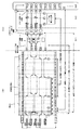
図21は従来の液晶表示装置の構成を示した図6の603ソースドライバ、605表示領域、606マルチプレクサからなり、ソース線群を2101、ゲート線群を2102で示している。
【0023】
図は簡略化のため、マルチプレクサの左上部分に相当するソース線4本、ゲート線8本からなる一部分を示し、ソースドライバの出力端子としてはST1およびST2で示す2出力分、マルチプレクサのスイッチ素子はソース線数相当分のみを表し、その他はこの部分の繰り返しの構成であるので省略している。
【0024】
表示領域については各画素の上に表示されたR、G、Bが各画素がもつ色の属性を、後続の数字は表示領域の行番号を、従ってゲート線の行番号を、+−は、ある1画面の液晶セルが保持している電圧極性をそれぞれ示している。
【0025】
また2103はマルチプレクサ制御信号でCTL0とCTL1で示し、前記マルチプレクサの各スイッチ素子のゲートに図のように接続されている。マルチプレクサの各スイッチ素子はMPに続く2桁の数字で表し、10位の数字は接続されているソース線の番号を、1位の数字は制御信号の番号を表す。またマルチプレクサの各スイッチ素子のソースはソースドライバに、ドレインはソース線に接続されている。ソースドライバの各出力ST1,ST2は、2分されマルチプレクサを介して隣り合う各ソース線に接続されている構成である。
【0026】
図22は従来の液晶表示装置の駆動方法が行う制御を説明するタイミング図である。ここでは、N=4の場合の動作例を示す。図において、SP1、SP2はソースドライバ制御信号の中の一種で、ソースドライバの出力電圧の極性を制御する制御信号である。SP1のHIGH期間において、ST1が正極性、ST2が負極性の前記表示信号電圧または前記非表示信号電圧を、LOW期間でST1が負極性の、ST2が正極性のそれぞれを出力する。SQ1、SQ2は前記SP1、SP2で制御されたソースドライバ603の期間T01、T02などの前半と後半におけるST1、ST2の出力電圧の種類と極性を表している。ここで、Kは前記非表示信号電圧を、R、G、Bはそれぞれ表示色の属性をもつ前記表示信号電圧を、+−はそれぞれの電圧の極性を、それぞれ示している。Kで示す前記非表示信号電圧は前記信号変換部で、R=5/4=1.25倍速のレート変換で前記表示信号電圧に挿入された非画像信号に対するソースドライバの出力電圧を示している。
【0027】
SWPはソースドライバ制御信号の中の別の一種で、ソースドライバの出力のタイミングを制御する信号で、HIGH、LOW論理の立ち上がりおよび立ち下がり(矢印で図示)で、ソースドライバは出力を開始する。
【0028】
CTL0のHIGH期間で、ソース線S1、S4に接続されたマルチプレクサのスイッチ素子MP10、MP40が導通し、ST1の出力をS1に,ST2の出力をS4にそれぞれ供給し、LOW期間で供給を遮断する。同様に、CTL1のHIGH期間で、ソース線S2、S3に接続されたマルチプレクサのスイッチ素子MP21,MP31が導通し、ST1の出力をS2,ST2の出力をS3に、それぞれ供給し、LOW期間で供給を遮断する。
【0029】
S1P、S2Pなどは、こうした信号電圧の操作によって、前記表示信号電圧および前記非表示信号電圧がS1、S2など各ソース線に印加された結果生じた、S1、S2などの電位(Potential)の状態を示している。K、R、G、B、+、−の記号はSQ1、SQ2のそれぞれと同等である。ただし、K、R、G、Bに後続の数字はゲート線の行番号を示している。
【0030】
T01ないしT10は、N=4の場合のR倍速駆動の一期間であり、入力画像信号の1水平期間を1Hで表すと、NH/(N+1)に等しく、10周期で8Hである。
【0031】
信号電圧の流れについては、例えば、T01前半の期間に存在するSQ1のK+の非表示信号電圧は、SWPの当期頭の立ち上がりで出力され、CTL0のHIGHで導通しているマルチプレクサのスイッチ素子を介してソース線S1上のS1が持つ電気的容量(例えば前記TFT203や前記浮遊容量206など、S1に属する全容量)に印加されて、S1Pは記号K+の非表示信号電圧となる。T01の後半では、CTL0がLOWとなり、ソース線S1上のマルチプレクサのスイッチ素子が遮断され、K+の非表示信号電圧がT01の期間末までS1上に存在する。続くT02前半の期間では、SQ1のR+の表示信号電圧が、同様の過程を経てソース線S1に印加され、R+の表示信号電圧がT02の期間末まで存在する。一方、並行して、期間T01の後半からT03前半の期間では、SQ1上のK−と続くG−の各非表示信号電圧、表示信号電圧が、SWPの立ち下がりで出力され、ソース線S2に印加され、一定の電位が存在することとなる。以降、同様の経過でT01からT10までを1周期とするソース線S1,S2の電位変化が繰り返される。SQ2、S3P、S4Pの状態も同様である。
【0032】
一方、図21のゲート線群2102は、前記駆動パルス生成部からのゲートドライバ制御信号を受けてゲートドライバが生成するゲート線ドライブパルスで駆動される。図4に示すG1P、G2P・・などがそれであり、それぞれゲート線G1,G2・・に印加される。画素TFT203などのオン電位を越える期間、例えば図4のTKWの期間および後続の高電位期間に、該当する画素のTFTがオン状態となり、液晶セルに、図22に示されたソース線電位の充電を行う(以降、書き込みと呼ぶ)。
【0033】
従来の1例として、G1〜G4の4本のゲート線を前記TKWの期間(図22のT01の2KNH前の期間、K=正の整数、この例ではN=4)において同時選択し、G1〜G4上の全ての画素に前記非表示信号電圧を書き込み、所定期間{(2K―1)NH}後の4H以内の時間でR、G、Bの前記各表示信号電圧を各ゲート線上の画素セルに順次、書き込み完了する。次のG5〜G8の4本のゲート線については、4H遅れて、同様の動作を繰り返す。このとき、ソース線上の電位の極性は図22に示されるように逆転している。この動作を全ゲート線にわたって1フレ−ムで完了させる。このように、表示領域にある全てのゲート線が1フレーム期間に2回ずつ選択され、各ゲート線上の画素に前記表示信号電圧と、前記非表示信号電圧が1回ずつ書き込まれる。
【0034】
次のフレームでは、画素電圧の極性が逆転するように、SP1、SP2の位相を180度移相する。以上が従来例での1カラム反転、4ライン反転、かつフレーム反転のCR駆動方法である。
【0035】
ソースドライバの制御と出力操作の方法は、多くの方式があり、また公知であり、本発明とは直接関係しない。またゲートのドライブ条件である前記TKWや常数Kの設定、R倍速のNの設定や動作の詳細などについても同様であるので、ここではこれ以上の説明は行わない。
【0036】
上記の動作により、周期的に表示信号電圧と非表示信号電圧を書き込むことができ、非表示信号電圧の電圧を適当に与えることで、OCB液晶セルの逆転移を防止することができる。
【0037】
【発明が解決しようとする課題】
しかしながら、上記の駆動においては、ソースドライバからソース線への非表示信号電圧印加時間がT01、またはT06、またはこれらの2KNH前後に位置する期間の前半と後半に別れること、および、マルチプレクサの遮断期間で発生するソース線の開放状態とが原因で発生する、図23、図5に示す課題があった。図23(a)はソース線の電位変動の過渡状況を示している。図中の記号は図22と同一である。例えば、T01期間のSQ1、S1P、S2Pに注目すると、T01前半で、SQ1上のK+がソース線S1に印加された時、S1にはS1Pに見られる正方向の電位変動が発生していることを上向きの矢印が示している。
【0038】
また、T01後半で、SQ1上のK−がソース線S2に印加された時、S2にはS2Pに見られる負方向の電位変動が発生していることを下向きの矢印が示している。期間T06においてはそれぞれ、逆方向の変動である。SQ2、S3P,S4Pについても同様の変動がある。実際には、その他の期間においても、各ソース線へのR、G、Bの前記表示信号電圧印加による変動があるが、前述の通り、表示信号電圧の電圧値は非表示信号電圧以下であり、かつ画素信号内容で小幅で変化しているので、影響が軽く、簡略化のため、ここでは考察対象に入れないでおくこととする。
【0039】
相隣るソース線どうしは、図2に示すC1RとC2L、C2RとC3Lなど、TFTドレイン電極を挟み直列接続された容量で電気的に結合されている。また、各画素もその両側に存在するソース線とはこれらの浮遊容量で電気的に結合されている。
【0040】
従って、上記ソース線の電位変動は、各ソース線の両側の画素、および両側のソース線に比較的大きな影響をもたらすことがある。
【0041】
図23(b)のOFF画素とは、前記表示信号電圧又は前記非表示信号電圧が一旦書き込まれた画素であって、その後、1フレーム毎の次の前記表示信号電圧又は前記非表示信号電圧の書き込みが始まる迄の期間のそれらの画素のことである。換言すれば、その時、203TFTがOFFとなっている画素である。
【0042】
図23(b1)に示すように、T01後半のS2PのK−の変動が、S1,S2間に存在するすべてのOFF画素に負方向の影響をもたらす。
【0043】
これをOFF画素への影響と呼び、矢印で極性を示している。また、この期間では、ソース線S1はマルチプレクサからみて開放(オープン)状態にある。従って、同時に、この期間で開放状態のS1に、前記OFF画素より、同等の負方向の影響を与える。これを前段オープンソース線への影響として図に示している。同様に、T01後半のS3PのK+の変動が、S3,S4間に存在するすべてのOFF画素に正方向の影響をもたらし、かつ、開放状態のS4に、正方向の影響を与える。S2,S3間のOFF画素については、S2P、S3Pが互いに逆方向に変動するため相殺しあって、C2R≒C3Lであれば、影響は少ないので黒四角で示している。S4、S5間のOFF画素については、S4P、S5Pに変動がないので、無印である。
【0044】
このS1,S4に生じた変動は、次のT02〜T05におけるVSの書き込み電圧に重畳されるが、*VSとの極性が逆であるので、−1と評価する。
【0045】
TO1前半のS1PのK+およびS4PのK−による変動は、この時オープン状態にあるSLS2およびS3に対し、影響はするが、S2,S3では直後のK−、K+のVBが供給されるため、その影響は解消され、T02以降のVS書き込みに影響しないので、図23(b1)のS2,S3に対する評価点は、0となる。
【0046】
次にT02でVSが書き込まれた画素は、T03以降、1フレーム後のBK書き込みまでOFF画素であるが、その間に、SLから受ける影響を考える。その影響は期間D〜Fの繰り返しであるから、この期間で評価する。
【0047】
図23(b2)は、各SLの期間D〜FでのBKによる変動を、期間圧縮して示しているが、期間平均では、*OFF画素への影響はないので、3に対する評価点は、0となる。
【0048】
次にT02で表示信号電圧が書き込まれた画素は、T03以降、1フレーム後の非表示信号電圧書き込みまでOFF画素であるが、その間に、ソース線から受ける影響を考える。その影響は期間D〜Fの繰り返しであるから、この期間で評価する。
【0049】
図23(b2)は、各ソース線の期間D〜Fでの非表示信号電圧による変動を、期間圧縮して示しているが、期間平均では、前記OFF画素への影響はないので、評価点は、0となる。
【0050】
以上より、1フレームでみた非表示信号電圧書き込みによる、画素への影響は図23(b3)に示すように、(b1)、(b2)の合計となり、i=1,2,3・・として、j=4i―3、i=4iに該当するソース線Sj上の画素において、本来あるべく値より透過率が高く、即ち、輝度として高くなる。図5は表示画像をイメージした図であり、図の(a)が、R、G、Bの各画素として本来の一定の輝度で動作している場合だとすると、図の(b)のように適当な視距離から見たときの表示ムラのない画像となるが、従来例における図23の(b3)の結果として、図(c1)のような実体像で、図(c2)のような視認像となる。即ち、従来例において、2本ごとの縦筋という課題があった。
【0051】
また、従来例のカラム反転駆動の場合、ソース線電圧として、+K〜−Kの電圧レンジが必要で、表示信号電圧の最大値が非表示信号電圧に等しいか、ほぼ等しいために、図22の例えば、T01期間におけるSQ1のK+からK−、T01からT02にかけてのK−からR+などなど、SP1、SP2の短かい周期に対応しうる大きな出力能力(スルーレート、ソース線ew Rate)が求められ、時にソース線充電能力、従って画素書き込み能力が不足し、画像の表示品位劣化を招いていた。
【0052】
逆に言えば、極めて高コストのソースドライバが必要とされる。
【0053】
さらには、CR駆動のための非表示信号電圧として、1種類で、R、G、Bの各液晶セルの逆転移防止を賄わねばならず、表示品位の向上に限度があった。
【0054】
特に、近年の液晶パネルは大型化、高精細化しており、ソース線数、画素の数の増大、両者の接近などによる浮遊容量の増加で、上記干渉問題の悪化、画素の充電時間不足を招く傾向にある。
【0055】
それ故、本発明の目的は、上記の課題を解決し、良好な映像を表示することが可能な液晶表示装置の駆動方法および液晶表示装置を提供することである。
【0056】
【課題を解決するための手段】
この課題を解決するために第1の発明は、複数のソース線と、複数のゲート線と、該ソース線と該ゲート線の交点に対応してマトリクス状に配置された画素セルと、で構成された表示領域を有する液晶パネルが組み込まれた表示装置の駆動方法であって、
入力画像信号を水平レート変換し、該変換によって生じた余裕時間に非表示信号を生成し、かつ該非表示信号を変換後の入力画像信号である表示信号に挿入する信号変換部と、
入力された同期信号から各種制御パルスを生成する駆動パルス生成部と、
前記信号変換部および前記駆動パルス生成部からの各種信号を受け、前記表示信号および前記非表示信号を所定の電圧値に変換して表示信号電圧および非表示信号電圧として出力するソースドライバと、
前記駆動パルス生成部からの制御信号を受け、前記ゲート線に駆動電圧を供給するゲートドライバと、
前記ソースドライバと前記表示領域との間に配置され、前記ソースドライバからの前記表示信号電圧および前記非表示信号電圧を受けて、複数本の前記ソース線に時分割で切り換えて供給するマルチプレクサ部とを具備し、
1画像の表示周期である1フレーム期間内に、前記表示領域内の全画素セルに、前記1画像に対応する画素信号電圧でもある前記表示信号電圧と、前記表示信号電圧とは別の非画素信号電圧でもある前記非表示信号電圧または更に別の電圧である補償電圧とのどちらか一方を書き込む際に、前記表示領域内における4の倍数より1および2少ない順列に配置された隣り合う一対の前記ソース線について、前記ソースドライバと前記表示領域間で配線の交差部を設けたことを特徴とする。
【0057】
これにより、画像信号書き込み時間の短縮を避け、画像劣化を排除するとともに、表示信号電圧、非表示信号電圧の書き込みをも容易たらしめ、同時に、ソースドライバの出力能力(ソース線ew Rateなど)を下げることができる効果がある。
【0058】
第2の発明は、第1の発明に対して、すべての前記ソース線に対し、前記非表示信号電圧を印加した後、所定期間内に、前記画素の複数行に対応する前記表示信号電圧を順次、前記ソース線に印加することを特徴とする。
【0059】
これにより、更にソースドライバの充電能力が改善され、従って表示信号電圧、非表示信号電圧書き込みの改善につながると同時に、表示品位の改善となる効果がある。
【0060】
第3の発明は、第2の発明に対して、所定の前記ソース線に供給される前記非表示信号電圧の、所定の基準電位に対する前記非表示信号電圧の極性を、該非表示信号電圧に続き、同じ前記ソース線に供給される前記表示信号電圧の、該所定の基準電位に対する極性と同一の極性とすることを特徴とする。
【0061】
これにより、更に、表示信号電圧書き込みを容易たらしめる効果がある。
【0062】
第4の発明は、第2の発明に対して、複数の前記ゲート線の同時選択期間において、所定の前記ソース線に供給される前記非表示信号電圧の、所定の基準電位に対する極性を、該非表示信号電圧に続き、同じ前記ソース線に供給される前記表示信号電圧の、該所定の基準電位に対する極性と同一とし、かつ前記非表示信号電圧を隣り合う前記ソース線に対して異極性とすることを特徴とする。
【0063】
これにより、第4の発明は、第2の発明に対して、表示品位の改善となる効果がある。
【0064】
第5の発明は、第1の発明に対して、前記補償電圧を前記ソース線に印加する補償電圧印加手段を前記マルチプレクサ部と前記表示領域間に配置し、前記ソースドライバより出力される前記表示信号電圧と同期した所定の期間内に、該補償電圧印加手段より前記補償電圧を前記全ソース線に印加することを特徴とする。
【0065】
これにより、第5の発明は、第1の発明に対して、黒(補償電圧)の書き込みをも容易たらしめ、最適な補償電圧が液晶パネルに供給でき、表示品位を更に改善できる効果がある。
【0066】
第6の発明は、第5の発明に対して、すべての前記ソース線に対し、前記補償電圧を印加した後、所定期間内に、前記画素の複数行に対応する前記表示信号電圧を順次、前記ソース線に印加することを特徴とする。
【0067】
これにより、第5の発明に対して、ソースドライバの充電能力が改善され、従って表示信号電圧、非表示信号電圧書き込みの改善につながると同時に、更なる表示品位の改善となる効果がある。
【0068】
第7の発明は、第5ないし第6のいずれかの発明に対して、所定の前記ソース線に供給される前記補償電圧の、所定の前記ソース線に供給される極性を、該補償電圧を印加した後に続き、同じ前記ソース線に供給される前記表示信号電圧と同一の極性とすることを特徴とする。
【0069】
これにより、第5ないし第6のいずれかの発明に対して、表示信号電圧書き込みを更に容易たらしめる効果がある。
【0070】
第8の発明は、第5ないし第6のいずれかの発明に対して、複数の前記ゲート線の同時選択期間において、所定の前記ソース線に供給される前記補償電圧の、所定の基準電位に対する極性を、該補償電圧に続き、同じ前記ソース線に供給される前記表示信号電圧の極性と同一とし、かつ隣り合う前記ソース線に対して、異極性とすることを特徴とする。
【0071】
これにより、第5ないし第6のいずれかの発明に対して、表示品位の改善となる効果がある。
【0072】
第9の発明は、第5の発明に対して、前記補償電圧を2種以上に複数化するとともに、電圧値および極性の組み合わせを2種以上に選定したことを特徴とする。
【0073】
これにより、第5の発明に対して、色別画素毎の黒(補償電圧)書き込み量の最適化が可能となり、表示品位の更なる改善となる効果がある。
【0074】
第10の発明は、第9の発明に対して、前記補償電圧の一部または全部について可変調節ができる構成とするとともに、前記液晶パネルの特性に合わせて電圧設定したことを特徴とする。
【0075】
これにより、第9の発明に対して、液晶パネルの対環境特性や個体差に対して、黒(補償電圧)書き込み量の最適化が可能となり、表示品位の更なる改善となる効果がある。
【0076】
第11の発明は、第9ないし第10のいずれかの発明に対して、R、G、Bのいずれかの色の表示に対応したソース線に対し、同じ色に対応する全てのソース線に対しては、同一電圧値に設定した前記補償電圧を供給することを特徴とする。
【0077】
これにより、第9の発明ならびに第10の発明に対して、R、G、B毎の特性に適応した黒(補償電圧)書き込み量の最適化が可能となり、表示品位の更なる改善となる効果がある。
【0078】
第12の発明は、第5ないし第11のいずれかの発明に対して、前記補償電圧の一部または全部の絶対値を、前記非表示信号電圧の絶対値より大とすることを特徴とする。
【0079】
これにより、第5ないし第11の発明に対して、更なる、黒(補償電圧)書き込み量の最適化が可能となり、表示品位の更なる改善となる効果がある。
【0080】
第13の発明は、第6ないし第12のいずれかの発明に対して、すべての前記ソース線に、前記補償電圧を同時に印加する期間において、同時に前記マルチプレクサに、同じ前記ソース線に供給される次の前記表示信号電圧と所定の基準電位に対して同一極性の前記非表示信号電圧を印加することを特徴とする。
【0081】
これにより、第6ないし第12の発明に対して、更なる、表示信号電圧書き込みを容易たらしめ、表示品位の更なる改善となる効果がある。
【0082】
第14の発明は、第2ないし第13のいずれかの発明に対して、前記ソースドライバと前記マルチプレクサ間に交差部を設けることを特徴とする。
【0083】
第15の発明は、第1ないし第14のいずれかの発明に対して、液晶セルがOCBであることを特徴とする。
【0084】
【発明の実施の形態】
(第1の実施形態)
図7は、本発明の第1の実施形態に係る液晶表示装置の構成を示す図、図10は、その構成の一部を示す図、図1は、タイミングを示した図、図12は駆動方法が行う制御による事象を説明するタイミング図である。
【0085】
以下、図1、図7、図10、図12を参照してその駆動を説明する。
【0086】
なお、第1の実施形態に係る液晶表示装置の構成は、図6の従来の実施形態に係る液晶表示装置における、信号変換部601を701に、駆動パルス生成部602を702に、ソースドライバ603を703に置き換えた構成である。その他の構成は同等であり、同一の参照番号を付して、説明を省略する。
【0087】
また、図10は、図7の703ソースドライバ、605表示領域、606マルチプレクサからなり、ソース線群を1001、マルチプレクサ制御信号を1003で示している。605表示領域の内部は図21より簡略化している。ソース線群1001の一部であって、ソースドライバ703とマルチプレクサ606の間でS2、S3を交差させた部分をソース線交差部1004としている。従って、従来と異なって、ST1はソース線S1,S3に、ST2はソース線S2,S4に信号電圧を供給する。
【0088】
以下、図1において、本発明の制御と動作について説明する。
【0089】
図1に使用の記号は、従来例のそれらと同一である。
【0090】
図において、ST1、ST2の信号出力として、従来例とGとBを入れ替えている。この操作は、公知として、ソースドライバのRGB出力選択機能で容易に変更できるので詳細を省略する。また、ソースドライバの出力電圧極性制御信号であるSP1,SP2は、その繰り返し周期を、従来例より10分の1に低くしている。これにより、T01〜T05、T06〜T10の期間でソースドライバの出力極性は同一である。
【0091】
図1(a)が第1の実施形態に係るタイミング図であり、従来例での説明と同様の制御操作により、SP1〜SP4について、従来例と同一の結果が得られることが示されている。
【0092】
この場合のソース線の変動とOFF画素への影響について、図12に示している。結果として、図12(b1)、(b2)、(b3)は従来例の図23のそれらと同一である。
【0093】
以上のように、第1の実施形態に係る液晶表示装置の駆動方法によれば、ソースドライバの出力極性を頻繁に変える必要がないので、表示信号電圧の書き込みが早く実行でき、画像信号書き込み時間の短縮を避け、画像劣化を排除するとともに、画像信号の書き込みをも容易たらしめる効果、あるいは、ソースドライバの出力能力(Slew Rateなど)を下げることができる効果がある。
【0094】
(第2の実施形態)
本発明の第2の実施形態に係る液晶表示装置の構成は、第1の実施形態と同一の図7、図10であるので、説明は省略し、図1(b)について、本発明の第2の実施形態に係る制御と動作を説明する。第1の実施形態と異なる部分は、マルチプレクサ制御信号CTL0、CTL1のパルス波形である。図1(c)のCTL0,CTL1は2NH周期の中のT01、T06の期間を通して常にHIGHであることである。このパルス信号は、信号変換部が内部で生成する非表示信号電圧挿入用制御パルスと論理的にORをとれば容易に生成できるものであり、本発明とは直接関係しないのでこれ以上の説明は行わない。
【0095】
これらのCTL0、CTL1を用いて、第1の実施形態と同様の制御操作により、SP1〜SP4について、第1の実施形態と類似の結果が得られることが図1(b)に示されている。第1の実施形態と異なるのは、S2P、S3P上のK、G4,G8,B4,B8の部分である。第1の実施形態と違って、T01の前半の時間に、S2P、S3Pに非表示信号電圧がソース線に供給される。従って、図13(a)に示すように、T01におけるソース線の変動として、隣り合うソース線どうしのどの一対で見ても、同時でかつ逆極性であるので、OFF画素への影響は、図13(b1)のように打ち消しあい、実質発生しない。また各ソース線も期間T01でオープン状態にはならないので、ソース線への影響も発生しない。また、その後の非表示信号電圧書き込み時のソース線の変動状況も図13(b2)のように相殺されて、平均0となるので全体として図(b3)に示すように、どのSL上の画素についてもBK書き込みの影響による輝度差が出ないと言える。
【0096】
なお、*G4、B4など他と比べてT/2(T=T01〜T10)の時間しかVSが存在しない部分があるが、実際にどの画素へのVS書き込み時間であっても、MPX606が導通してSDよりVSが供給されているT/2であり、残りの時間は重要な意味を持たないので何ら支障は生じない。
【0097】
期間Tをとおして存在するR、G、Bは、その後半部は単にSL上の残留電位に過ぎないといえ、画素への書き込みにそれほど寄与していない。
【0098】
また図1(d)に示すCTL0、CTL1の場合は、T01,T06の期間で前半だけHIGHで、後半はLOWであるが、S1P〜S4Pについては、上記図1(c)の場合と同一である。
【0099】
従って、図5の(b)のように表示ムラのない均一な画像が得られる。
【0100】
以上のように、第2の実施形態に係る液晶表示装置の駆動方法によれば、第1の実施形態に加えて、輝度の不均一による2本毎に見える縦筋を除去できる効果がある。
【0101】
(第3の実施形態)
本発明の第3の実施形態に係る液晶表示装置の構成は、第2の実施形態と同一の図7であるが、図11のように、ソース線の構成が一部、異なる。第2の実施形態では、S2,S3のソース線の交差部1004がソースドライバとマルチプレクサの間に位置しているが、第3の実施形態では、前記交差部がマルチプレクサと表示領域の間に構成されている。本発明による駆動方法の制御は、第2の実施形態のそれである図1(b)と同じであるが、その過渡的な動作において、以下の点が異なり、表示品位にも差異が出る場合がある。
【0102】
ソース線交差部には図10、図11のCsで示すように、対向面積と内在する絶縁材料の誘電率に比例し、対向距離に反比例の層間容量が存在する。このCsは液晶パネルの構造上、無視できない値になり、両ソース線の干渉課題を引き起こすことがある。図10の場合は、マルチプレクサのMP31,MP21がOFFの時も、ONの時も、このCsにST1、ST2の信号電圧が加わる。また、ソース線からみて、マルチプレクサ31,マルチプレクサ12がOFFの時、S2,S3間にはCsが存在しない状態となる。一方、本案の図11では、マルチプレクサのMP31,MP21がOFFの時には、ST1、ST2からの電圧供給はなく、ソース線S2,S3間にCsが存在する状態となる。
【0103】
図1のタイミング図の、例えば、T02期間で上記状態を説明すると、第2の実施形態の場合は、T02前半でCsにSQ1,SQ2のR+,R−が印加されており、後半でB+,G−に変わる。またT02前半では、ソース線S2にはK−、S3にはK+が残留しているが、T02後半では、上記Csの電位差の影響を受けたG−がS2に、同じくB+がS3に印加される。この影響度はソースドライバの出力能力に依存することは言うまでもない。
【0104】
一方、第3の実施形態の場合は、ソース線S2,S3間のCsには、T02前半でK−、K+が残留しており、後半でSQ2のG−、SQ3のB+が、S2,S3,Csに加わる。
【0105】
T03以下についても、SQ1、SQ2、S2P、S3Pの各期間前半の電圧状態が、Csの位置による後半に対する影響が同様に決まる。
【0106】
1フレーム全体で言えることは、第2の実施形態では、i=1,2,3・・として、j=4i―3、i=4i―2に該当するソース線Sj上の画素がその画素のそれぞれ左、右(従って他の色)の表示信号電圧に相当する輝度レベルの影響を受ける場合があるが、第3の実施形態では、非表示信号電圧またはその画素の一行上の同系の影響しか受けないという利点がある。
【0107】
従って、第3の実施形態に係る液晶表示装置の駆動方法によれば、第2の実施形態に加えて、画像劣化が除去できる効果がある。
【0108】
(第4の実施形態)
図8は、本発明の第4の実施形態に係る液晶表示装置の構成を示す図、図14は、その構成の一部を示す図、図15はタイミング図である。 以下、図8、図14、図15を参照してその駆動を説明する。
【0109】
図8に示す第4の実施形態に係る液晶表示装置の構成は、図6の従来の実施形態に係る液晶表示装置における、信号変換部601を801に、駆動パルス生成部602を802に、ソースドライバ603を803に、電源部607を807に置き換えた構成とし、更に、808補償電圧印加部を、前記マルチプレクサ606と表示領域605の間に追加・配置し、電源部807より前記表示信号電圧あるいは前記非表示信号電圧とは別の補償電圧を供給する構成である。その他の構成は同等であり、同一の参照番号を付して、説明を省略する。
【0110】
また、図14は、図8の803ソースドライバ、605表示領域、606マルチプレクサからなり、ソース線群を1401、マルチプレクサ制御信号を1403、ソース線交差部を1004でそれぞれ示している。
【0111】
また、追加の補償電圧印加部808を制御する補償電圧印加制御信号1407、+−両極性の補償電圧を供給する電源線1408を含む追加の全体構成としての補償電圧印加手段を1406で示している。図中の黒+、黒−はそれぞれ補償電圧の正、負の電圧を表す記号とする。
【0112】
補償電圧印加部808は、ソース線1本当たり、2個のスイッチ素子を配備し、それぞれを、ソース線と、+および−の電源線1408との間に接続した構成とし、その制御端子に補償電圧印加制御信号1407を図のように接続している。各スイッチ素子をSWに続く2桁の数字で表し、10位の数字はソース線の番号を、1位の数字は補償電圧印加制御信号の番号を表している。補償電圧印加制御信号1407はCTLP0〜CTLP3の4種である。
【0113】
以下、図15において、本発明の制御と動作について説明する。
【0114】
図15において、CTLP以外の記号は本発明の実施形態1ないし3と同じである。前述の第2の実施形態の説明と異なる部分はSQ1、SQ2において、T01、T06の期間で非表示信号電圧を表すK+、K−の“記号”が“不問”の2字に変わっていることと、CTLP0〜CTLP3の補償電圧印加制御信号が追加されていることである。そしてCTL0,CTL1は、これらの期間、LOWであって、動作として、各ソース線からソースドライバを切り離していることであり、更に、S1P〜S4Pには、これらの期間で、CTLP0〜CTLP3のHIGHの期間に補償電圧印加部の各スイッチ素子の動作により、補償電圧印加部の電源ライン1408より、黒+又は黒−の印加が行われた結果を示していることである。この期間のSWPに関しては、立ち上がり、立ち下がりの有無が問われないことはソースドライバ同様明白である。その他の期間は第2の実施形態と基本的に同一である。
【0115】
ソース線への、黒+、黒−の印加の操作を説明すると、T01の期間では、CTLP0,CTLP3がHIGHであり、SW10、SW40、およびSW23,SW33がON状態、CTLP1,CTLP2がLOWであり、SW11,SW41,およびSW22,SW32がOFF状態であるので、S1、S3に黒+、また、S2、S4に黒−がそれぞれ印加、充電される。T06の期間ではCTLPのHIGH、LOWの関係がT01と逆転し、従ってSWのON、OFFが逆転するので、それぞれのソース線に印加される補償電圧の極性も逆転となる。
【0116】
以上のような構成と駆動の方法により、第2の実施形態と同様のタイミング駆動ができ、従って、縦筋の無い良好な表示品位が得られる。
【0117】
ここでは、補償電圧の値として、黒+、黒−で表記し、第1ないし第3の実施形態の非表示信号電圧に相当する前記OCB液晶セルの逆転移防止の補償電圧を想定して説明したが他の目的に展開できるものでもある。
【0118】
この補償電圧は電圧値として、前記信号変換部など信号系統の誓約を受けることなく、独立に比較的自由に設定できる効果がある。例えば、非表示信号電圧はソースドライバの出力段のダイナミックレンジ幅から、上限の制約があるが、補償電圧はソースドライバの出力段耐圧まで、大きく設定できること、また可変として液晶パネルの対環境特性や個体差への対応を容易ならしめる効果がある。
【0119】
以上、第4の実施形態に係る液晶表示装置の駆動方法によれば、表示品位を劣化させることなく、補償電圧の最適な供給が液晶パネルに供給できる。
【0120】
(第5の実施形態)
本発明の第5の実施形態に係る液晶表示装置の構成は、第4の実施形態と同一の図8であるが、図16のように、ソース線の構成が一部、異なる。第4の実施形態では、S2,S3のソース線の交差部1404がソースドライバとマルチプレクサの間に位置しているが、第5の実施形態では、ソース線の交差部1604は、マルチプレクサと補償電圧印加部の間に構成されている。本発明による駆動方法の制御は、第4の実施形態のタイミング図15と同じであるが、その過渡的な動作において、第3の実施形態で説明した、第3と第2の実施形態との場合と同様の差異があり、表示品位にも差異が出る場合がある。
【0121】
ただし、第5の実施形態においては、前記非表示信号電圧のK+−が補償電圧の黒+−に取って変わっている点が異なる。従って、第4の実施形態では、1フレーム全体では、i=1,2,3・・として、j=4i―3、i=4i―2に該当するソース線Sj上の画素がその画素のそれぞれ左、右(従って他の色)の表示信号電圧に相当する輝度レベルの影響を受ける場合があるが、第5の実施形態では、補償電圧またはその画素の一行上の同系の影響しか受けないという利点がある。従って、第5の実施形態に係る液晶表示装置の駆動方法によれば、第4の実施形態に加えて、画像劣化が除去できる効果がある。
【0122】
(第6の実施形態)
本発明の第6の実施形態に係る液晶表示装置の構成は、第4の実施形態と同一の図8であるが、図17のように、ソース線の構成が一部、異なる。第4の実施形態では、S2,S3のソース線の交差部1404がソースドライバとマルチプレクサの間に位置しているが、第6の実施形態では、ソース線の交差部1704は補償電圧印加部と表示領域の間に構成されている。これに伴い、ソース線S2,S3に係わる補償電圧印加部のスイッチ素子SWが入れ替わり、かつCTLP2,CTLP3との結線を変更し、前述の付与法にて番号が付されている。この補償電圧印加手段を1706として示している。
【0123】
本発明による駆動方法の制御は、第4の実施形態のタイミング図15と同じであるが、また、第5の実施形態のその過渡的な動作と同一であるので説明を省略する。第6の実施形態においても、第5の実施形態と同様に、補償電圧またはその画素の一行上の同系の影響しか受けないという利点があり、画像劣化が除去できる効果がある。
【0124】
(第7の実施形態)
図3の電圧−透過率曲線で示される特性を持つOCBパネルは、電圧無印加時は白表示となる、いわゆるノーマリーホワイトの液晶パネルである。そのため、表示性能、具体的にはコントラスト性能を高めるためには、いかに透過率の低い黒表示を行うかが重要となる。この最低透過率を与える際の印加電圧であるが、OCBパネルの特性から、R、G、Bの画素ごとにその電圧値が異なるケースがある。
【0125】
そこで、本発明の第7の実施形態に係る液晶表示装置の駆動方法は、上記の課題を解決するために、R、G、Bごとに最適な前記補償電圧を画素に印加するようにしたものである。
【0126】
図9は、本発明の第7の実施形態に係る液晶表示装置の構成を示す図、図18は、その構成の一部を示す図、図19はタイミングを示す図である。
【0127】
以下、図9、図18、図19を参照してその駆動を説明する。
【0128】
図9に示す第7の実施形態に係る液晶表示装置の構成は、図8の第4の実施形態に係る液晶表示装置における、電源部807を907に置き換えた構成である。
【0129】
また、図18は、図9の803ソースドライバ、605表示領域、606マルチプレクサ、補償電圧印加部808からなる。なお、補償電圧印加部808を制御する補償電圧印加制御信号1407、+−両極性のR、G、B別の補償電圧を供給する電源線1808を含む全体構成としての補償電圧印加手段を1806で示している。図中のR黒+、R黒−はそれぞれ、Rに係わる補償電圧の正、負の電圧を表す記号とし、G、Bについても同様とする。つまり、補償電圧印加手段以外は第4の実施例、図14と同一であり、CTL、CTLPも同一である。補償電圧印加手段1806の各スイッチ素子は、そのスイッチが接続されたソース線がもつ、R、G、Bの属性に合わせて、それぞれ同一の属性の電源線に接続されている。
【0130】
以下、図19において、本発明の制御と動作について説明する。
【0131】
図19において、前述の第4の実施形態のタイミング図と異なる部分はS1P〜S2Pにおいて、T01、T06の期間で補償電圧を表す黒+、黒−の“記号”の前に、前記R、G、Bに係わる補償電圧を意味する“R”、“G”、“B”の文字が加わっていることである。
【0132】
ソース線への、R、G、B、各黒+、各黒−の印加の操作については、第4の実施形態における説明と同様の制御操作により、S1P〜S4Pに示すR、G、B、の黒+−が得られる。
【0133】
以上のような構成と駆動の方法により、R、G、B毎に最適な補償電圧を画素に印加することにより、第4の実施形態以上に、良好な表示品位が得られる。
【0134】
(第8の実施形態)
本発明の第8の実施形態に係る液晶表示装置の構成は、第4の実施形態と同一であるが、図14のマルチプレクサ606のTFTスイッチ素子のOFF時の電極容量Cm1〜Cm4などを用いて、ソースドライバの充電能力を補おうとするもので、タイミング図20により、その駆動方法を説明する。
【0135】
その前に、図20(a)を用いて、第4の実施形態における課題を説明する。図20(a)のCm1P〜Cm4Pは第4の実施形態における、前記Cm1〜Cm4の電位状態を示す図である。ここでSP1,P2、SWPのソースドライバ制御信号、およびSQ1、SQ2のソースドライバST1、ST2の出力電圧は実施形態4のタイミング図15と同一である。2NHの周期の中で、T01,T06以外の期間においてはSQ1、SQ2の出力電圧がCm1〜Cm4に充電されているが、T01,T06の期間においては、SWPの立ち上がり、もしくは立ち下がりがないため、ソースドライバからの出力が印加されないので、その期間の前の表示信号電圧が充電されたままである。この状態から、T02,またはT07のSWPの立ち上がりに制御されて、ソースドライバ出力は、S1,S4のソース線と、これら全Cmに対し、従前の逆極性の表示信号電圧電位を乗り越えて表示信号電圧電圧を供給することになり、高い出力能力が求められる。第4の実施形態の課題であった。
【0136】
本第8の実施形態においては、第4の実施形態の図15におけるCTLおよびCTLPと、第1の実施形態の図1に示されるSQ1,SQ2,SWPを用いて、図20(b1)、(b2)に示すタイミング構成としている。この制御動作について、(b1)のT01、T06以外の部分は上記第4の実施形態の場合と同様である。T01,T06の期間では、CTL0,CTL1がLOWでマルチプレクサがすべてOFFであり、マルチプレクサの全Cmに、SWPの制御でソースドライバより、次に来る表示信号電圧と同極性の非表示信号電圧が印加・充電される。従って、ソースドライバにとって、次のT02、T07の表示信号電圧の全Cmへの充電がし易くなる。ソース線の電位については、図20(b2)に示すように第4の実施形態の図15のそれと同一であるが、厳密には、上記Cmへの予備充電に相当した充電の改善がなされる。
【0137】
以上、第8の実施形態に係る液晶表示装置の駆動方法によれば、ソース線への、従って画素への表示信号電圧書き込み能力の改善という効果がある。
【0138】
【発明の効果】
以上説明したように、本発明の液晶表示装置の駆動方法および液晶表示装置によれば、表示信号電圧書き込み時間の短縮を避け、表示信号電圧、非表示信号電圧、補償電圧の書き込みを容易たらしめ、画像劣化を排除し、縦筋などの表示品位を解消するとともに、ソースドライバの出力能力(Slew Rateなど)を下げることができ、駆動コストを削減でき、特に液層セルがOCBである液晶パネルに対して、逆転移を防止し、これによる画面輝度低下の影響を極力小さくできる効果がある。
【0139】
また、色別に補償電圧が異なる液晶セルに対しても、液晶パネルの対環境特性や個体差に対しても、黒(補償電圧)書き込み量の最適化が可能となり、この逆転移防止などのための最適な補償電圧が液晶パネルに供給でき、表示品位の更なる改善ができる効果がある。
【図面の簡単な説明】
【図1】本発明の第1、第2、第3の実施形態に係る液晶表示装置の駆動方法が行う制御を説明するタイミング図
【図2】液晶表示装置の表示領域の構成を示す図
【図3】OCBの電位−透過率曲線を示す図
【図4】ゲート線の駆動方法を説明する図
【図5】表示領域における表示画面の均一性を説明する図
【図6】従来の液晶表示装置の構成を示した図
【図7】本発明の第1、第2、第3の実施形態に係る液晶表示装置の構成を示す図
【図8】本発明の第4、第5、第6、第8の実施形態に係る液晶表示装置の構成を示す図
【図9】本発明の第7の実施形態に係る液晶表示装置の構成を示す図
【図10】本発明の第1、第2の実施形態に係る液晶表示装置の構成の一部を示す図
【図11】本発明の第3の実施形態に係る液晶表示装置の構成の一部を示す図
【図12】本発明の第1の実施形態に係る液晶表示装置の駆動方法が行う制御による事象を説明するタイミング図
【図13】本発明の第2の実施形態に係る液晶表示装置の駆動方法が行う制御による事象を説明するタイミング図
【図14】本発明の第4、第8の実施形態に係る液晶表示装置の構成の一部を示す図
【図15】本発明の第1の実施形態に係る液晶表示装置の駆動方法が行う制御を説明するタイミング図
【図16】本発明の第5の実施形態に係る液晶表示装置の構成の一部を示す図
【図17】本発明の第6の実施形態に係る液晶表示装置の構成の一部を示す図
【図18】本発明の第7の実施形態に係る液晶表示装置の構成の一部を示す図
【図19】本発明の第7の実施形態に係る液晶表示装置の駆動方法が行う制御を説明するタイミング図
【図20】本発明の第8の実施形態に係る液晶表示装置の駆動方法が行う制御を説明するタイミング図
【図21】従来の液晶表示装置の構成の一部を示す図
【図22】従来の液晶表示装置の駆動方法が行う制御を説明するタイミング図
【図23】従来の液晶表示装置の駆動方法が行う制御による事象を説明する図
【符号の説明】
201 ソース線
202 ゲート線
203 TFT
204 画素
205 対向駆動部
206 TFTに接続された画素電極とソース線との間に存在する浮遊容量
301 逆転移防止のための所定電位を挿入しない場合の電位−透過率曲線
302 逆転移防止のための所定電位を挿入したCR駆動の場合の電位−透過率曲線
303 臨界電位
304 最も高い透過率の時の電位
305 最も低い透過率の時の電位
601、701、801 信号変換部
602、702,802 駆動パルス生成部
603、703,803 ソースドライバ
604、ゲートドライバ
605 液晶パネルの表示領域
606 マルチプレクサ部
607、807、907 電源部
808 補償電圧印加部
1001、1101、1401、1601、1701、2101 ソース線群
1003、1103、1403,2103 マルチプレクサ制御信号
1004、1104,1404、1604、1704 ソース線交差部
1406、1706、1806 補償電圧印加制御手段
1407、 補償電圧印加制御信号
1408、1808 補償電圧印加電源線[0001]
BACKGROUND OF THE INVENTION
The present invention relates to an active matrix liquid crystal display device driving method and a liquid crystal display device, and more particularly to a liquid crystal display device driving method using an OCB (Optically self-compensated birefringence) liquid crystal mode having a wide viewing angle and high-speed response. The present invention relates to a liquid crystal display device.
[0002]
[Prior art]
As is well known, a large number of liquid crystal display devices are used as screen display devices such as computer devices, but in the future, use in TV applications is also expected. However, the currently widely used TN (Twisted Nematic) mode has a narrow viewing angle and an insufficient response speed, and has a great display performance when used as a TV, such as a reduction in contrast due to parallax and blurring of moving images. There are challenges.
[0003]
In recent years, research on the OCB mode is progressing instead of the TN mode. OCB has characteristics such as a wide viewing angle and high-speed response compared to TN, and can be said to be a display mode more suitable for natural moving image display.
[0004]
Hereinafter, a conventional method for driving a liquid crystal display device and a liquid crystal display device will be described.
[0005]
In FIG. 2, S1, S2,... Indicated by 201 are source lines, G1, G2,... Indicated by 202 are gate lines, 203 is a thin film transistor (hereinafter referred to as TFT) as a switching element, and a drain electrode of each TFT. Are connected to a pixel electrode in the
[0006]
The counter electrode of each pixel is connected to the
[0007]
Next, FIG. 6 showing a configuration relating to driving of a conventional liquid crystal display device will be described.
[0008]
The display signal and the non-display signal are sent to the source driver from the signal conversion unit, and the source driver converts the display signal and the non-display signal under the control of the source driver control signal sent from the drive pulse generation unit. The polarity and voltage appropriate for each pixel are converted and output as a display signal voltage and a non-display signal voltage.
[0009]
606 is arranged between the source driver and the display area, and under the control of a multiplexer control signal sent from the drive pulse generation unit, the display signal voltage and the non-display signal voltage from the source driver, The multiplexer unit distributes and supplies to the plurality of source lines while switching in a time division manner.
[0010]
In addition, the gate driver is synchronized with the output of the display signal voltage or the non-display signal voltage from the source driver under the control of the gate driver control signal sent from the drive pulse generator, and The on potential or off potential of the TFT is supplied.
[0011]
A
[0012]
The voltage applied to both ends of the liquid crystal cell such as each
[0013]
The polarity of the voltage applied to both ends of the liquid crystal cell is defined by the positive / negative of the difference between the Vcom and the display signal voltage or the non-display signal voltage applied to each
[0014]
Such a driving method is the same whether an OCB cell is used or a TN type cell is used. However, the OCB cell needs to be driven peculiar to the TN type cell at the start-up stage in which video display is started.
[0015]
The OCB cell has a bend orientation corresponding to a state where image display is possible and a splay orientation corresponding to a state where image display is not possible. In order to shift from the splay alignment to the bend alignment (hereinafter referred to as transition), a unique drive such as applying a high voltage for a certain time is required. However, the driving related to this transition is not directly related to the present invention, and will not be described further.
[0016]
Even if the OCB cell is once changed to bend alignment by the above unique driving, if the voltage of a predetermined level or more is not applied for a predetermined time or longer, the bend alignment cannot be maintained and returns to the splay alignment (hereinafter, referred to as “the bend alignment”). This phenomenon is called reverse transition).
[0017]
In order to suppress the occurrence of reverse transition, it is described in JP-A No. 11-109921 and Journal of the Japanese Liquid Crystal Society, April 25, 1999 (Vol. 3. No. 2) P99 (17) to P106 (24). As is known, it is known that a high voltage may be periodically applied. The non-display signal voltage corresponds to this high potential, and the occurrence of reverse transition can be suppressed by applying the non-display signal voltage periodically by the driving described below. The non-display signal voltage is generally the maximum display signal voltage corresponding to black display from the viewpoint of the effect of suppressing the occurrence of reverse transition and the display image quality.
[0018]
Hereinafter, driving that periodically applies a high potential and suppresses reverse transition is referred to as CR (Cyclic Reset) driving.
[0019]
FIG. 3 shows a general OCB potential-transmittance curve.
[0020]
In FIG. 3, 301 is a potential-transmittance curve when a predetermined potential for preventing reverse transition is not inserted, 302 is a potential-transmittance curve when CR driving is performed with a predetermined potential for preventing reverse transition, and 303 is The critical potential Vth, 304 at which the reverse transition from the bend alignment to the splay alignment occurs without reverse transition prevention, 304 is the potential at the highest transmittance (white potential), and 305 is the potential at the lowest transmittance (black potential). ). If reverse transition prevention is not performed, the splay orientation is restored at Vth or lower, so that an appropriate transmittance cannot be obtained. Therefore, it is necessary to drive at a potential higher than Vth. However, as shown in FIG. However, the transmittance is low, and sufficient luminance cannot be obtained.
[0021]
On the other hand, liquid crystals represented by OCB and TN need to perform so-called AC driving, but the specific configuration is not described in the above-mentioned Japanese Patent Application Laid-Open No. 11-109921 or the above-mentioned Journal of the Japanese Liquid Crystal Society. It is not possible to specify what AC reversal should be performed. Therefore, the CR driving when the combination of inversion for each line and inversion for each frame, which is the most general driving, is performed will be described with reference to FIGS. 21, 22, and 23 as a conventional example.
[0022]
21 includes the 603 source driver, 605 display area, and 606 multiplexer shown in FIG. 6 showing the configuration of a conventional liquid crystal display device.
[0023]
For the sake of simplification, the figure shows a part consisting of four source lines and eight gate lines corresponding to the upper left part of the multiplexer, and the output terminal of the source driver is for two outputs indicated by ST1 and ST2, and the switch elements of the multiplexer are Only the portion corresponding to the number of source lines is shown, and the others are omitted because they are the repeated configuration of this portion.
[0024]
Regarding the display area, R, G, and B displayed on each pixel indicate the color attribute of each pixel, the subsequent numbers indicate the row number of the display area, and accordingly the line number of the gate line, + − The voltage polarities held by a liquid crystal cell of one screen are shown.
[0025]
[0026]
FIG. 22 is a timing chart for explaining the control performed by the driving method of the conventional liquid crystal display device. Here, an operation example in the case of N = 4 is shown. In the figure, SP1 and SP2 are types of source driver control signals, and are control signals for controlling the polarity of the output voltage of the source driver. In the HIGH period of SP1, ST1 outputs the display signal voltage or the non-display signal voltage having a positive polarity, ST2 outputs a negative polarity, and ST1 outputs a negative polarity and ST2 has a positive polarity in the LOW period. SQ1 and SQ2 represent the types and polarities of the output voltages of ST1 and ST2 in the first half and the second half of periods T01 and T02 of the
[0027]
SWP is another type of source driver control signal, and is a signal for controlling the output timing of the source driver. The source driver starts output at the rise and fall (shown by arrows) of HIGH and LOW logic.
[0028]
In the HIGH period of CTL0, the switch elements MP10 and MP40 of the multiplexer connected to the source lines S1 and S4 are turned on, the output of ST1 is supplied to S1, the output of ST2 is supplied to S4, and the supply is cut off during the LOW period. . Similarly, in the HIGH period of CTL1, the switch elements MP21 and MP31 of the multiplexer connected to the source lines S2 and S3 become conductive, the ST1 output is supplied to S2 and the ST2 output to S3, and the LOW period is supplied. Shut off.
[0029]
S1P, S2P, etc. are states of potentials such as S1, S2, which are generated as a result of applying the display signal voltage and the non-display signal voltage to the respective source lines such as S1, S2 by the operation of such signal voltages. Is shown. The symbols K, R, G, B, +, and − are equivalent to SQ1 and SQ2, respectively. However, the numbers following K, R, G, and B indicate the row numbers of the gate lines.
[0030]
T01 to T10 are one period of R double speed driving in the case of N = 4. When one horizontal period of the input image signal is represented by 1H, it is equal to NH / (N + 1) and is 8H in 10 periods.
[0031]
Regarding the flow of the signal voltage, for example, the non-display signal voltage of K + of SQ1 existing in the first half period of T01 is output at the beginning of the SWP period, and passes through the switch element of the multiplexer that is conductive at HIGH of CTL0. And applied to the electric capacitance of S1 on the source line S1 (for example, all capacitances belonging to S1, such as the
[0032]
On the other hand, the
[0033]
As a conventional example, four gate lines G1 to G4 are simultaneously selected in the TKW period (period before 2KNH of T01 in FIG. 22, K = positive integer, N = 4 in this example), and G1 The non-display signal voltage is written to all the pixels on G4 and the display signal voltages of R, G, and B are applied to the pixels on each gate line in a time within 4H after a predetermined period {(2K-1) NH}. Writing to the cells is completed sequentially. For the next four gate lines G5 to G8, the same operation is repeated with a delay of 4H. At this time, the polarity of the potential on the source line is reversed as shown in FIG. This operation is completed in one frame across all gate lines. In this way, all the gate lines in the display area are selected twice in one frame period, and the display signal voltage and the non-display signal voltage are written once to the pixels on each gate line.
[0034]
In the next frame, the phases of SP1 and SP2 are shifted by 180 degrees so that the polarity of the pixel voltage is reversed. The above is the conventional CR driving method for one column inversion, four line inversion, and frame inversion.
[0035]
There are many methods for controlling the source driver and the output operation, which are well known and are not directly related to the present invention. The same applies to the setting of the TKW and constant K, which is the gate drive condition, the setting of N for the R double speed, and the details of the operation, and will not be described further here.
[0036]
Through the above operation, the display signal voltage and the non-display signal voltage can be periodically written, and the reverse transition of the OCB liquid crystal cell can be prevented by appropriately applying the voltage of the non-display signal voltage.
[0037]
[Problems to be solved by the invention]
However, in the above driving, the non-display signal voltage application time from the source driver to the source line is divided into the first half and the second half of the period located around T01, T06, or these 2KNH, and the multiplexer cutoff period 23 and FIG. 5 occurred due to the open state of the source line generated in FIG. FIG. 23A shows the transient state of the potential fluctuation of the source line. The symbols in the figure are the same as those in FIG. For example, paying attention to SQ1, S1P, and S2P in the T01 period, when K + on SQ1 is applied to the source line S1 in the first half of T01, a potential fluctuation in the positive direction seen in S1P occurs in S1. Is indicated by an upward arrow.
[0038]
Further, in the second half of T01, when K− on SQ1 is applied to the source line S2, a downward arrow indicates that a potential fluctuation in the negative direction seen in S2P occurs in S2. In the period T06, the fluctuations are in the reverse direction. There are similar variations in SQ2, S3P, and S4P. Actually, there are fluctuations due to the application of the display signal voltage of R, G, and B to each source line in other periods, but as described above, the voltage value of the display signal voltage is equal to or less than the non-display signal voltage. In addition, since the pixel signal content changes in a small range, the influence is light and for simplification, it is not considered here.
[0039]
Adjacent source lines are electrically coupled by a capacitor connected in series with the TFT drain electrode interposed therebetween, such as C1R and C2L, C2R and C3L shown in FIG. Each pixel is also electrically coupled to the source line existing on both sides by these stray capacitances.
[0040]
Therefore, the potential fluctuation of the source line may have a relatively large influence on the pixels on both sides of each source line and the source lines on both sides.
[0041]
The OFF pixel in FIG. 23B is a pixel in which the display signal voltage or the non-display signal voltage is once written, and then the next display signal voltage or the non-display signal voltage for each frame. Those pixels in the period until writing starts. In other words, it is a pixel in which 203 TFT is OFF at that time.
[0042]
As shown in FIG. 23 (b1), the variation of K2 of S2P in the latter half of T01 has a negative influence on all OFF pixels existing between S1 and S2.
[0043]
This is called the influence on the OFF pixel, and the polarity is indicated by an arrow. In this period, the source line S1 is in an open state as viewed from the multiplexer. Accordingly, at the same time, the S1 that is in the open state during this period has an equal negative influence from the OFF pixel. This is shown in the figure as an effect on the previous open source line. Similarly, the variation in S3P K + in the latter half of T01 has a positive influence on all OFF pixels existing between S3 and S4, and has a positive influence on S4 in the open state. The OFF pixels between S2 and S3 are offset because S2P and S3P fluctuate in opposite directions. If C2R≈C3L, the influence is small, and the black pixel is shown. The OFF pixel between S4 and S5 is not marked because there is no change in S4P and S5P.
[0044]
The fluctuations generated in S1 and S4 are superimposed on the VS write voltage in the next T02 to T05, but since the polarity is opposite to * VS, it is evaluated as -1.
[0045]
The fluctuations due to S1P K + and S4P K- in the first half of TO1 affect SLS2 and S3 in the open state at this time, but in S2 and S3, the immediately following K- and K + VB are supplied. Since the influence is eliminated and VS writing after T02 is not affected, the evaluation score for S2 and S3 in FIG.
[0046]
Next, a pixel to which VS is written at T02 is an OFF pixel from T03 to BK writing after one frame, and the influence received from SL during that time is considered. Since the influence is a repetition of the periods D to F, the evaluation is performed in this period.
[0047]
FIG. 23 (b2) shows the fluctuation due to BK in the periods D to F of each SL while compressing the period, but the average for the period does not affect the * OFF pixel, so the evaluation score for 3 is 0.
[0048]
Next, the pixel to which the display signal voltage is written at T02 is an OFF pixel from T03 until the non-display signal voltage is written after one frame, and the influence received from the source line during that time is considered. Since the influence is a repetition of the periods D to F, the evaluation is performed in this period.
[0049]
FIG. 23 (b2) shows the fluctuation caused by the non-display signal voltage in the periods D to F of each source line in a compressed period. However, the average of the period does not affect the OFF pixels. Becomes 0.
[0050]
From the above, the influence on the pixel due to the non-display signal voltage writing in one frame is the sum of (b1) and (b2) as shown in FIG. 23 (b3), and i = 1, 2, 3,. , J = 4i−3, and pixels on the source line Sj corresponding to i = 4i have the transmittance as high as possible, that is, the luminance as high as possible. FIG. 5 is an image of a display image. If (a) in FIG. 5 is a case where each pixel of R, G, and B is operating at an original constant luminance, an appropriate one as shown in (b) of FIG. The image has no display unevenness when viewed from a wide viewing distance, but as a result of (b3) in FIG. 23 in the conventional example, a real image as in FIG. (C1) and a visual image as in FIG. (C2) It becomes. That is, in the conventional example, there is a problem of vertical bars every two lines.
[0051]
In the case of the column inversion driving of the conventional example, a voltage range of + K to −K is necessary as the source line voltage, and the maximum value of the display signal voltage is equal to or substantially equal to the non-display signal voltage. For example, a large output capability (slew rate, source line ew Rate) that can correspond to a short period of SP1 and SP2, such as K + to K- of SQ1 in the T01 period, K- to R + from T01 to T02, etc. is required. In some cases, the source line charging ability, and hence the pixel writing ability, is insufficient, and the display quality of the image is deteriorated.
[0052]
Conversely, a very expensive source driver is required.
[0053]
Furthermore, one type of non-display signal voltage for CR drive must be provided to prevent reverse transition of each of the R, G, and B liquid crystal cells, and there has been a limit to improving display quality.
[0054]
In particular, liquid crystal panels in recent years have become larger in size and higher in definition, resulting in an increase in stray capacitance due to an increase in the number of source lines, the number of pixels, and the proximity of both, leading to worsening of the interference problem and insufficient pixel charging time. There is a tendency.
[0055]
Therefore, an object of the present invention is to solve the above-described problems and provide a driving method of a liquid crystal display device and a liquid crystal display device capable of displaying a good image.
[0056]
[Means for Solving the Problems]
In order to solve this problem, a first invention includes a plurality of source lines, a plurality of gate lines, and pixel cells arranged in a matrix corresponding to the intersections of the source lines and the gate lines. A driving method of a display device in which a liquid crystal panel having a display area is incorporated,
A signal conversion unit that performs horizontal rate conversion on the input image signal, generates a non-display signal in a margin time generated by the conversion, and inserts the non-display signal into a display signal that is the input image signal after conversion;
A drive pulse generator for generating various control pulses from the input synchronization signal;
A source driver that receives various signals from the signal conversion unit and the drive pulse generation unit, converts the display signal and the non-display signal into predetermined voltage values, and outputs them as a display signal voltage and a non-display signal voltage;
A gate driver that receives a control signal from the drive pulse generator and supplies a drive voltage to the gate line;
A multiplexer unit disposed between the source driver and the display region, receiving the display signal voltage and the non-display signal voltage from the source driver, and switching and supplying to the plurality of source lines in a time-sharing manner; Comprising
A non-pixel different from the display signal voltage, which is also a pixel signal voltage corresponding to the one image, and the display signal voltage in all pixel cells in the display area within one frame period which is a display cycle of one image. When writing either the non-display signal voltage, which is also a signal voltage, or a compensation voltage, which is another voltage, a pair of adjacent ones arranged in a permutation that is 1 and 2 less than a multiple of 4 in the display area The source line is characterized in that a wiring intersection is provided between the source driver and the display area.
[0057]
This avoids shortening the image signal writing time, eliminates image degradation, facilitates writing of display signal voltages and non-display signal voltages, and at the same time increases the output capability of the source driver (source line ew Rate, etc.). There is an effect that can be lowered.
[0058]
According to a second invention, in contrast to the first invention, after the non-display signal voltage is applied to all the source lines, the display signal voltages corresponding to a plurality of rows of the pixels are applied within a predetermined period. The voltage is sequentially applied to the source line.
[0059]
As a result, the charging capability of the source driver is further improved, so that the display signal voltage and the non-display signal voltage writing are improved, and at the same time, the display quality is improved.
[0060]
According to a third aspect of the present invention, the polarity of the non-display signal voltage with respect to a predetermined reference potential of the non-display signal voltage supplied to the predetermined source line is continued from the non-display signal voltage. The display signal voltage supplied to the same source line has the same polarity as that of the predetermined reference potential.
[0061]
This further has the effect of facilitating writing of the display signal voltage.
[0062]
According to a fourth aspect of the present invention, the polarity of the non-display signal voltage supplied to a predetermined source line with respect to a predetermined reference potential in the simultaneous selection period of the plurality of gate lines is different from the second aspect. Following the display signal voltage, the display signal voltage supplied to the same source line has the same polarity with respect to the predetermined reference potential, and the non-display signal voltage has a different polarity with respect to the adjacent source line. It is characterized by that.
[0063]
As a result, the fourth aspect of the invention has the effect of improving display quality over the second aspect of the invention.
[0064]
5th invention is different from 1st invention in that compensation voltage application means for applying the compensation voltage to the source line is arranged between the multiplexer unit and the display region, and the display output from the source driver. The compensation voltage is applied to all the source lines by the compensation voltage application means within a predetermined period synchronized with the signal voltage.
[0065]
As a result, the fifth aspect of the invention makes it easier to write black (compensation voltage) than the first aspect of the invention, so that the optimum compensation voltage can be supplied to the liquid crystal panel, and the display quality can be further improved. .
[0066]
According to a sixth aspect of the present invention, in contrast to the fifth aspect, after applying the compensation voltage to all the source lines, the display signal voltages corresponding to the plurality of rows of pixels are sequentially applied within a predetermined period. It is applied to the source line.
[0067]
As a result, the charging capability of the source driver is improved with respect to the fifth aspect of the invention, so that the display signal voltage and the non-display signal voltage writing are improved, and at the same time, the display quality is further improved.
[0068]
The seventh invention 5th or 6th One of The polarity of the compensation voltage supplied to a predetermined source line is applied to the predetermined source line after applying the compensation voltage, and then supplied to the same source line. It has the same polarity as the display signal voltage.
[0069]
This 5th or 6th One of In contrast to this invention, there is an effect that the writing of the display signal voltage is made easier.
[0070]
The eighth invention 5th or 6th One of According to the invention, in the simultaneous selection period of the plurality of gate lines, the polarity of the compensation voltage supplied to the predetermined source line with respect to the predetermined reference potential is set to the same source line following the compensation voltage. The polarity of the display signal voltage to be supplied is the same as that of the adjacent source line, and the polarity is different from that of the adjacent source line.
[0071]
This 5th or 6th One of The present invention has an effect of improving the display quality.
[0072]
The ninth invention is characterized in that the compensation voltage is divided into two or more types and the combination of the voltage value and the polarity is selected to two or more types with respect to the fifth invention.
[0073]
This makes it possible to optimize the black (compensation voltage) writing amount for each pixel for each color with respect to the fifth invention, thereby further improving the display quality.
[0074]
The tenth aspect of the invention is characterized in that, with respect to the ninth aspect of the invention, a part or all of the compensation voltage can be variably adjusted, and the voltage is set in accordance with the characteristics of the liquid crystal panel.
[0075]
Thereby, with respect to the ninth aspect, the black (compensation voltage) writing amount can be optimized with respect to the environmental characteristics and individual differences of the liquid crystal panel, and the display quality can be further improved.
[0076]
In an eleventh aspect of the present invention, in contrast to any of the ninth to tenth aspects of the invention, all source lines corresponding to the same color are provided for source lines corresponding to display of any of R, G, and B colors. On the other hand, the compensation voltage set to the same voltage value is supplied.
[0077]
As a result, the black (compensation voltage) writing amount adapted to the characteristics for each of R, G, and B can be optimized with respect to the ninth and tenth inventions, and the display quality can be further improved. There is.
[0078]
The twelfth invention is characterized in that the absolute value of a part or all of the compensation voltage is larger than the absolute value of the non-display signal voltage with respect to any of the fifth to eleventh inventions. .
[0079]
As a result, the black (compensation voltage) writing amount can be further optimized with respect to the fifth to eleventh inventions, and the display quality can be further improved.
[0080]
In a thirteenth aspect of the present invention, in contrast to any one of the sixth to twelfth aspects, in the period in which the compensation voltage is simultaneously applied to all the source lines, the multiplexer is supplied to the same source line at the same time. The non-display signal voltage having the same polarity with respect to the next display signal voltage and a predetermined reference potential is applied.
[0081]
As a result, the display signal voltage can be easily written to the sixth to twelfth inventions, and the display quality can be further improved.
[0082]
The fourteenth invention is characterized in that, with respect to any one of the second to thirteenth inventions, an intersection is provided between the source driver and the multiplexer.
[0083]
The fifteenth aspect of the invention is characterized in that the liquid crystal cell is OCB with respect to any one of the first to fourteenth aspects of the invention.
[0084]
DETAILED DESCRIPTION OF THE INVENTION
(First embodiment)
7 is a diagram showing a configuration of the liquid crystal display device according to the first embodiment of the present invention, FIG. 10 is a diagram showing a part of the configuration, FIG. 1 is a diagram showing timing, and FIG. 12 is driving It is a timing diagram explaining the event by the control which a method performs.
[0085]
Hereinafter, the drive will be described with reference to FIG. 1, FIG. 7, FIG. 10, and FIG.
[0086]
Note that the configuration of the liquid crystal display device according to the first embodiment is the same as that of the liquid crystal display device according to the conventional embodiment of FIG. 6, the
[0087]
10 includes the 703 source driver, the 605 display area, and the 606 multiplexer shown in FIG. 7. The source line group is denoted by 1001 and the multiplexer control signal is denoted by 1003. The interior of the
[0088]
Hereinafter, the control and operation of the present invention will be described with reference to FIG.
[0089]
The symbols used in FIG. 1 are the same as those in the conventional example.
[0090]
In the figure, as a signal output of ST1 and ST2, the conventional example and G and B are interchanged. Since this operation can be easily changed by the RGB output selection function of the source driver as is well known, the details are omitted. In addition, SP1 and SP2, which are output voltage polarity control signals of the source driver, have a repetition cycle that is 1/10 lower than that of the conventional example. As a result, the output polarity of the source driver is the same during the period of T01 to T05 and T06 to T10.
[0091]
FIG. 1A is a timing chart according to the first embodiment, and shows that the same result as in the conventional example can be obtained for SP1 to SP4 by the same control operation as described in the conventional example. .
[0092]
FIG. 12 shows the variation of the source line and the influence on the OFF pixel in this case. As a result, FIGS. 12 (b1), (b2), and (b3) are the same as those of FIG. 23 of the conventional example.
[0093]
As described above, according to the driving method of the liquid crystal display device according to the first embodiment, since it is not necessary to frequently change the output polarity of the source driver, the display signal voltage can be written quickly, and the image signal writing time can be increased. In this case, there is an effect that the image signal can be easily written or the output capability of the source driver (Slew Rate, etc.) can be reduced.
[0094]
(Second Embodiment)
Since the configuration of the liquid crystal display device according to the second embodiment of the present invention is the same as that of the first embodiment shown in FIGS. 7 and 10, the description thereof is omitted, and FIG. The control and operation according to the second embodiment will be described. The difference from the first embodiment is the pulse waveforms of the multiplexer control signals CTL0 and CTL1. CTL0 and CTL1 in FIG. 1C are always HIGH throughout the periods T01 and T06 in the 2NH cycle. This pulse signal can be easily generated by logically ORing with the non-display signal voltage insertion control pulse generated internally by the signal conversion unit, and is not directly related to the present invention. Not performed.
[0095]
Using these CTL0 and CTL1, it is shown in FIG. 1B that similar results to the first embodiment can be obtained for SP1 to SP4 by the same control operation as in the first embodiment. . The difference from the first embodiment is the portions of K, G4, G8, B4, and B8 on S2P and S3P. Unlike the first embodiment, the non-display signal voltage is supplied to the source lines in S2P and S3P in the first half of T01. Therefore, as shown in FIG. 13 (a), as a source line variation at T01, any pair of adjacent source lines is simultaneously and opposite in polarity, and therefore the influence on the OFF pixel is as shown in FIG. 13 (b1) cancels each other and does not substantially occur. In addition, since each source line is not opened in the period T01, the source line is not affected. Further, the fluctuation state of the source line at the time of subsequent writing of the non-display signal voltage is canceled as shown in FIG. 13 (b2) and becomes an average of 0, so that the pixel on which SL as a whole as shown in FIG. 13 (b3). It can be said that there is no luminance difference due to the influence of BK writing.
[0096]
Note that there are parts where VS exists only for T / 2 (T = T01 to T10) compared to others such as * G4, B4, etc., but the
[0097]
R, G, and B that exist during the period T do not contribute so much to writing to the pixel because the latter half is merely a residual potential on the SL.
[0098]
In the case of CTL0 and CTL1 shown in FIG. 1 (d), only the first half is HIGH and the second half is LOW in the period of T01 and T06, but S1P to S4P are the same as those in FIG. 1 (c). is there.
[0099]
Therefore, a uniform image without display unevenness can be obtained as shown in FIG.
[0100]
As described above, according to the driving method of the liquid crystal display device according to the second embodiment, in addition to the first embodiment, there is an effect that vertical stripes appearing every two lines due to non-uniform luminance can be removed.
[0101]
(Third embodiment)
The configuration of the liquid crystal display device according to the third embodiment of the present invention is the same as that of the second embodiment shown in FIG. 7, but the configuration of the source lines is partially different as shown in FIG. In the second embodiment, the
[0102]
As shown by Cs in FIGS. 10 and 11, there is an interlayer capacitance that is proportional to the opposing area and the dielectric constant of the underlying insulating material and inversely proportional to the opposing distance, as indicated by Cs in FIGS. This Cs becomes a value that cannot be ignored due to the structure of the liquid crystal panel, and may cause an interference problem between the two source lines. In the case of FIG. 10, the signal voltages of ST1 and ST2 are applied to this Cs regardless of whether the multiplexers MP31 and MP21 are OFF or ON. When viewed from the source line, when the
[0103]
For example, in the timing diagram of FIG. 1, the above state will be described. In the second embodiment, R + and R− of SQ1 and SQ2 are applied to Cs in the first half of T02 and B +, Change to G-. In the first half of T02, K− remains in the source line S2 and K + remains in S3. However, in the latter half of T02, G− affected by the potential difference of Cs is applied to S2, and B + is also applied to S3. The Needless to say, the degree of influence depends on the output capability of the source driver.
[0104]
On the other hand, in the case of the third embodiment, K− and K + remain in Cs between the source lines S2 and S3 in the first half of T02, and G− in SQ2 and B + in SQ3 in S2 and S3 in the second half. , Cs.
[0105]
Also for T03 and below, the influence of the voltage state in the first half of each period of SQ1, SQ2, S2P, and S3P on the second half due to the position of Cs is similarly determined.
[0106]
What can be said for the entire frame is that in the second embodiment, i = 1, 2, 3,..., And the pixel on the source line Sj corresponding to j = 4i-3 and i = 4i-2 Each of them may be affected by the luminance level corresponding to the display signal voltage of the left and right (and hence other colors), but in the third embodiment, only the non-display signal voltage or the similar effect on one row of the pixel is affected. There is an advantage of not receiving.
[0107]
Therefore, according to the driving method of the liquid crystal display device according to the third embodiment, in addition to the second embodiment, there is an effect that image deterioration can be removed.
[0108]
(Fourth embodiment)
FIG. 8 is a diagram showing a configuration of a liquid crystal display device according to the fourth embodiment of the present invention, FIG. 14 is a diagram showing a part of the configuration, and FIG. 15 is a timing diagram. Hereinafter, the drive will be described with reference to FIG. 8, FIG. 14, and FIG.
[0109]
The configuration of the liquid crystal display device according to the fourth embodiment shown in FIG. 8 is the same as that of the liquid crystal display device according to the conventional embodiment shown in FIG. 6, with the
[0110]
14 includes the 803 source driver, the 605 display area, and the 606 multiplexer shown in FIG. 8. The source line group is indicated by 1401, the multiplexer control signal is indicated by 1403, and the source line intersection is indicated by 1004.
[0111]
Further,
[0112]
The compensation
[0113]
Hereinafter, the control and operation of the present invention will be described with reference to FIG.
[0114]
In FIG. 15, symbols other than CTLP are the same as those in the first to third embodiments of the present invention. The difference from the description of the second embodiment described above is that, in SQ1 and SQ2, the “symbols” of K + and K− representing the non-display signal voltages in the periods T01 and T06 have been changed to two letters “unquestioned”. The compensation voltage application control signals for CTLP0 to CTLP3 are added. CTL0 and CTL1 are LOW during these periods, and the operation is to disconnect the source driver from each source line. Further, S1P to S4P include HIGH of CTLP0 to CTLP3 during these periods. This is a result of applying black + or black− from the
[0115]
The operation of applying black + and black − to the source line will be explained. During the period T01, CTLP0 and CTLP3 are HIGH, SW10, SW40, SW23 and SW33 are ON, and CTLP1 and CTLP2 are LOW. Since SW11, SW41, and SW22, SW32 are in the OFF state, black + is applied to S1 and S3, and black- is applied to S2 and S4, respectively. During the period T06, the relationship between HIGH and LOW of CTLP is reversed with that of T01. Therefore, since ON and OFF of SW are reversed, the polarity of the compensation voltage applied to each source line is also reversed.
[0116]
With the configuration and driving method as described above, timing driving similar to that of the second embodiment can be performed, and therefore, a good display quality without vertical stripes can be obtained.
[0117]
Here, black + and black − are used as compensation voltage values, and the compensation voltage for preventing reverse transition of the OCB liquid crystal cell corresponding to the non-display signal voltage of the first to third embodiments is assumed. However, it can be developed for other purposes.
[0118]
This compensation voltage has an effect that it can be set relatively independently as a voltage value without receiving a commitment from the signal system such as the signal converter. For example, the non-display signal voltage has an upper limit from the dynamic range width of the output stage of the source driver, but the compensation voltage can be set large up to the output stage withstand voltage of the source driver. This has the effect of facilitating the handling of individual differences.
[0119]
As described above, according to the driving method of the liquid crystal display device according to the fourth embodiment, the optimum supply of the compensation voltage can be supplied to the liquid crystal panel without degrading the display quality.
[0120]
(Fifth embodiment)
The configuration of the liquid crystal display device according to the fifth embodiment of the present invention is the same as that of the fourth embodiment shown in FIG. 8, but the configuration of the source lines is partially different as shown in FIG. In the fourth embodiment, the
[0121]
However, the fifth embodiment is different in that the non-display signal voltage K + − is replaced by the compensation voltage black + −. Therefore, in the fourth embodiment, in one whole frame, i = 1, 2, 3,..., And pixels on the source line Sj corresponding to j = 4i-3 and i = 4i-2 are the respective pixels. Although it may be affected by the luminance level corresponding to the display signal voltage of the left and right (and therefore other colors), in the fifth embodiment, it is only affected by the compensation voltage or a similar effect on one row of the pixel. There are advantages. Therefore, according to the driving method of the liquid crystal display device according to the fifth embodiment, in addition to the fourth embodiment, there is an effect that image deterioration can be removed.
[0122]
(Sixth embodiment)
The configuration of the liquid crystal display device according to the sixth embodiment of the present invention is the same as that of the fourth embodiment shown in FIG. 8, but the configuration of the source lines is partially different as shown in FIG. In the fourth embodiment, the
[0123]
The control of the driving method according to the present invention is the same as that in the
[0124]
(Seventh embodiment)
The OCB panel having the characteristics shown by the voltage-transmittance curve in FIG. 3 is a so-called normally white liquid crystal panel that displays white when no voltage is applied. Therefore, in order to improve display performance, specifically, contrast performance, it is important how to perform black display with low transmittance. Although it is an applied voltage for giving this minimum transmittance, there are cases where the voltage value differs for each of R, G, and B pixels due to the characteristics of the OCB panel.
[0125]
Accordingly, in a driving method of a liquid crystal display device according to the seventh embodiment of the present invention, in order to solve the above-described problem, the optimum compensation voltage is applied to the pixel for each of R, G, and B. It is.
[0126]
FIG. 9 is a diagram showing a configuration of a liquid crystal display device according to a seventh embodiment of the present invention, FIG. 18 is a diagram showing a part of the configuration, and FIG. 19 is a diagram showing timing.
[0127]
Hereinafter, the drive will be described with reference to FIG. 9, FIG. 18, and FIG.
[0128]
The configuration of the liquid crystal display device according to the seventh embodiment shown in FIG. 9 is a configuration in which the
[0129]
18 includes the 803 source driver, the 605 display area, the 606 multiplexer, and the compensation
[0130]
Hereinafter, the control and operation of the present invention will be described with reference to FIG.
[0131]
In FIG. 19, the difference from the timing diagram of the fourth embodiment described above is that in S1P to S2P, R, G before the “symbol” of black +, black − representing the compensation voltage in the period of T01, T06. , B are added with letters “R”, “G”, and “B”, which mean compensation voltages.
[0132]
Regarding the operation of applying R, G, B, each black +, and each black- to the source line, R, G, B, and S shown in S1P to S4P are performed by the same control operation as described in the fourth embodiment. Of black +-is obtained.
[0133]
By applying the optimum compensation voltage for each of R, G, and B to the pixel by the above configuration and driving method, a better display quality than in the fourth embodiment can be obtained.
[0134]
(Eighth embodiment)
The configuration of the liquid crystal display device according to the eighth embodiment of the present invention is the same as that of the fourth embodiment, but the electrode capacitances Cm1 to Cm4 when the TFT switch elements of the
[0135]
Before that, the problem in the fourth embodiment will be described with reference to FIG. Cm1P to Cm4P in FIG. 20A are diagrams showing potential states of the Cm1 to Cm4 in the fourth embodiment. Here, the source driver control signals of SP1, P2, and SWP and the output voltages of the source drivers ST1 and ST2 of SQ1 and SQ2 are the same as those in the
[0136]
In the eighth embodiment, by using the CTL and CTLP in FIG. 15 of the fourth embodiment and SQ1, SQ2, and SWP shown in FIG. 1 of the first embodiment, FIG. 20 (b1), ( The timing configuration shown in b2) is adopted. Regarding this control operation, the portions other than T01 and T06 in (b1) are the same as in the case of the fourth embodiment. During the period of T01 and T06, CTL0 and CTL1 are LOW and all the multiplexers are OFF, and the non-display signal voltage having the same polarity as the next display signal voltage is applied to all Cm of the multiplexer from the source driver by SWP control.・ It is charged. Therefore, it becomes easy for the source driver to charge all Cm of the display signal voltages of the next T02 and T07. The potential of the source line is the same as that of FIG. 15 of the fourth embodiment as shown in FIG. 20 (b2). Strictly speaking, the charging corresponding to the preliminary charging to Cm is improved. .
[0137]
As described above, according to the driving method of the liquid crystal display device according to the eighth embodiment, there is an effect of improving the display signal voltage writing ability to the source line and thus to the pixel.
[0138]
【The invention's effect】
As described above, according to the liquid crystal display device driving method and the liquid crystal display device of the present invention, it is easy to write display signal voltage, non-display signal voltage, and compensation voltage while avoiding shortening the display signal voltage writing time. Liquid crystal panel that eliminates image degradation, eliminates display quality such as vertical streaks, lowers the output capability of the source driver (Slew Rate, etc.), reduces driving costs, and in particular the liquid layer cell is OCB On the other hand, there is an effect of preventing reverse transition and minimizing the influence of the decrease in screen brightness.
[0139]
In addition, the amount of black (compensation voltage) writing can be optimized for liquid crystal cells with different compensation voltages for different colors as well as for environmental characteristics and individual differences of the liquid crystal panel. The optimum compensation voltage can be supplied to the liquid crystal panel, and the display quality can be further improved.
[Brief description of the drawings]
FIG. 1 is a timing diagram illustrating control performed by a method for driving a liquid crystal display device according to first, second, and third embodiments of the present invention.
FIG. 2 is a diagram showing a configuration of a display area of a liquid crystal display device
FIG. 3 is a diagram showing a potential-transmittance curve of OCB.
FIG. 4 is a diagram illustrating a method for driving a gate line
FIG. 5 is a diagram for explaining the uniformity of the display screen in the display area;
FIG. 6 is a diagram showing a configuration of a conventional liquid crystal display device
FIG. 7 is a diagram showing a configuration of a liquid crystal display device according to first, second, and third embodiments of the present invention.
FIG. 8 is a diagram showing a configuration of a liquid crystal display device according to fourth, fifth, sixth, and eighth embodiments of the present invention.
FIG. 9 is a diagram showing a configuration of a liquid crystal display device according to a seventh embodiment of the present invention.
FIG. 10 is a diagram showing a part of the configuration of the liquid crystal display device according to the first and second embodiments of the present invention;
FIG. 11 is a diagram showing a part of the configuration of a liquid crystal display device according to a third embodiment of the present invention.
FIG. 12 is a timing chart for explaining an event due to control performed by the driving method of the liquid crystal display device according to the first embodiment of the present invention;
FIG. 13 is a timing chart for explaining an event caused by control performed by the driving method of the liquid crystal display device according to the second embodiment of the present invention.
FIG. 14 is a diagram showing a part of the configuration of a liquid crystal display device according to fourth and eighth embodiments of the present invention;
FIG. 15 is a timing chart for explaining control performed by the liquid crystal display device driving method according to the first embodiment of the present invention;
FIG. 16 is a diagram showing a part of the configuration of a liquid crystal display device according to a fifth embodiment of the present invention;
FIG. 17 is a diagram showing a part of the configuration of a liquid crystal display device according to a sixth embodiment of the present invention;
FIG. 18 is a diagram showing a part of the configuration of a liquid crystal display device according to a seventh embodiment of the present invention;
FIG. 19 is a timing chart for explaining control performed by the driving method of the liquid crystal display device according to the seventh embodiment of the present invention.
FIG. 20 is a timing chart for explaining control performed by a driving method of a liquid crystal display device according to an eighth embodiment of the present invention.
FIG. 21 is a diagram showing a part of the configuration of a conventional liquid crystal display device.
FIG. 22 is a timing chart for explaining control performed by a conventional liquid crystal display device driving method;
FIG. 23 is a diagram for explaining an event caused by control performed by a conventional liquid crystal display device driving method;
[Explanation of symbols]
201 Source line
202 Gate line
203 TFT
204 pixels
205 Opposite drive unit
206 Stray capacitance existing between the pixel electrode connected to the TFT and the source line
301 Potential-transmittance curve when a predetermined potential for preventing reverse transition is not inserted
302 Potential-transmittance curve in the case of CR driving with a predetermined potential inserted to prevent reverse transition
303 critical potential
304 Potential at highest transmittance
305 Potential at lowest transmittance
601, 701, 801 Signal converter
602, 702, 802 Drive pulse generator
603, 703, 803 Source driver
604, gate driver
605 LCD panel display area
606 Multiplexer section
607, 807, 907 Power supply
808 Compensation voltage application unit
1001, 1101, 1401, 1601, 1701, 2101 Source line group
1003, 1103, 1403, 2103 Multiplexer control signal
1004, 1104, 1404, 1604, 1704 Source line intersection
1406, 1706, 1806 Compensation voltage application control means
1407, Compensation voltage application control signal
1408, 1808 Compensation voltage application power supply line
Claims (15)
同じ色に対応する全てのソース線に対しては、同一電圧値に設定した前記補償電圧を供給することを特徴とする請求項9ないし10のいずれかに記載の液晶表示装置の駆動方法。For the source line corresponding to the display of any color of R, G, B
11. The driving method of a liquid crystal display device according to claim 9, wherein the compensation voltage set to the same voltage value is supplied to all source lines corresponding to the same color.
Priority Applications (8)
| Application Number | Priority Date | Filing Date | Title |
|---|---|---|---|
| JP2002096467A JP4154911B2 (en) | 2002-03-29 | 2002-03-29 | Method for driving liquid crystal display device and liquid crystal display device |
| KR1020037017092A KR100896598B1 (en) | 2002-03-29 | 2003-03-26 | LCD Display |
| PCT/JP2003/003698 WO2003083821A1 (en) | 2002-03-29 | 2003-03-26 | Liquid crystal display device |
| CNB038009110A CN100351888C (en) | 2002-03-29 | 2003-03-26 | Liquid crystal display device |
| US10/481,749 US7106284B2 (en) | 2002-03-29 | 2003-03-26 | Liquid crystal display device |
| EP03712974A EP1492077A4 (en) | 2002-03-29 | 2003-03-26 | LIQUID CRYSTAL DISPLAY DEVICE |
| CA002454039A CA2454039A1 (en) | 2002-03-29 | 2003-03-26 | Liquid crystal display device |
| TW092106889A TWI258614B (en) | 2002-03-29 | 2003-03-27 | Liquid crystal display device |
Applications Claiming Priority (1)
| Application Number | Priority Date | Filing Date | Title |
|---|---|---|---|
| JP2002096467A JP4154911B2 (en) | 2002-03-29 | 2002-03-29 | Method for driving liquid crystal display device and liquid crystal display device |
Publications (2)
| Publication Number | Publication Date |
|---|---|
| JP2003295834A JP2003295834A (en) | 2003-10-15 |
| JP4154911B2 true JP4154911B2 (en) | 2008-09-24 |
Family
ID=28671834
Family Applications (1)
| Application Number | Title | Priority Date | Filing Date |
|---|---|---|---|
| JP2002096467A Expired - Fee Related JP4154911B2 (en) | 2002-03-29 | 2002-03-29 | Method for driving liquid crystal display device and liquid crystal display device |
Country Status (8)
| Country | Link |
|---|---|
| US (1) | US7106284B2 (en) |
| EP (1) | EP1492077A4 (en) |
| JP (1) | JP4154911B2 (en) |
| KR (1) | KR100896598B1 (en) |
| CN (1) | CN100351888C (en) |
| CA (1) | CA2454039A1 (en) |
| TW (1) | TWI258614B (en) |
| WO (1) | WO2003083821A1 (en) |
Families Citing this family (31)
| Publication number | Priority date | Publication date | Assignee | Title |
|---|---|---|---|---|
| US7400306B2 (en) * | 2004-06-02 | 2008-07-15 | Au Optronics Corp. | Driving method for dual panel display |
| CN100403396C (en) * | 2004-10-08 | 2008-07-16 | 统宝光电股份有限公司 | Driving circuit, multi-panel display device using the same, and electronic device |
| JP2008033209A (en) * | 2005-09-28 | 2008-02-14 | Toshiba Matsushita Display Technology Co Ltd | Liquid crystal display device |
| JP2008015179A (en) * | 2006-07-05 | 2008-01-24 | Toshiba Matsushita Display Technology Co Ltd | Liquid crystal display |
| CN101123073B (en) * | 2006-08-09 | 2011-10-19 | 奇美电子股份有限公司 | Driving method of display panel and related device |
| JP4498337B2 (en) | 2006-10-17 | 2010-07-07 | 東芝モバイルディスプレイ株式会社 | Liquid crystal display |
| US20080180369A1 (en) * | 2007-01-26 | 2008-07-31 | Tpo Displays Corp. | Method for Driving a Display Panel and Related Apparatus |
| KR101340999B1 (en) | 2007-04-24 | 2013-12-13 | 엘지디스플레이 주식회사 | A liquid crystal display deivce and a method for driving the same |
| CN101373584B (en) * | 2007-08-21 | 2011-07-06 | 联咏科技股份有限公司 | source driver |
| JP4478899B2 (en) * | 2007-10-15 | 2010-06-09 | Nec液晶テクノロジー株式会社 | Display device, terminal device, display panel, and driving method of display device |
| US8446355B2 (en) | 2007-10-15 | 2013-05-21 | Nlt Technologies, Ltd. | Display device, terminal device, display panel, and display device driving method |
| CN101620830B (en) * | 2008-07-02 | 2011-12-21 | 联咏科技股份有限公司 | data drive |
| CN102087447B (en) * | 2009-12-04 | 2013-01-02 | 深圳华映显示科技有限公司 | Liquid crystal display device with double-gate-electrode drive architecture |
| US8573853B2 (en) | 2010-08-23 | 2013-11-05 | Tyco Electronics Corporation | Plug assembly |
| KR101878176B1 (en) * | 2011-10-06 | 2018-07-13 | 엘지디스플레이 주식회사 | Driving apparatus for image display device and method for driving the same |
| US10115357B2 (en) * | 2012-12-18 | 2018-10-30 | Apple Inc. | Display with soft-transitioning column driver circuitry |
| KR102233626B1 (en) * | 2014-09-15 | 2021-04-01 | 삼성디스플레이 주식회사 | Display device |
| JP2016184097A (en) | 2015-03-26 | 2016-10-20 | 株式会社ジャパンディスプレイ | Display device |
| CN104867468B (en) * | 2015-06-04 | 2017-05-03 | 武汉华星光电技术有限公司 | Display panel and display device |
| KR20170005291A (en) * | 2015-07-02 | 2017-01-12 | 삼성전자주식회사 | Output buffer circuit controling selw slope and source driver comprising the same and method of generating the source drive signal thereof |
| US10170072B2 (en) * | 2015-09-21 | 2019-01-01 | Apple Inc. | Gate line layout configuration |
| CN105590600A (en) * | 2015-12-15 | 2016-05-18 | 武汉华星光电技术有限公司 | Display and driving method thereof |
| CN105469765B (en) * | 2016-01-04 | 2018-03-30 | 武汉华星光电技术有限公司 | Multiplexing display driver circuit |
| TWI576812B (en) * | 2016-04-15 | 2017-04-01 | 友達光電股份有限公司 | Pixel driving circuit |
| CN105741809A (en) * | 2016-05-04 | 2016-07-06 | 武汉华星光电技术有限公司 | Liquid crystal display device and driving method thereof |
| TWI646514B (en) * | 2017-08-24 | 2019-01-01 | 友達光電股份有限公司 | Multiplexer applied to display device |
| TWI659407B (en) * | 2018-05-22 | 2019-05-11 | 友達光電股份有限公司 | Display device |
| KR102709389B1 (en) | 2020-02-28 | 2024-09-26 | 삼성디스플레이 주식회사 | Display device |
| CN111477136A (en) * | 2020-04-08 | 2020-07-31 | 福建华佳彩有限公司 | A power-saving display screen architecture and driving method |
| CN113781948B (en) * | 2021-09-24 | 2023-11-28 | 武汉华星光电技术有限公司 | Display panel and display device |
| CN113867061A (en) * | 2021-09-30 | 2021-12-31 | 上海天马微电子有限公司 | Array substrate, driving method of array substrate and display device |
Family Cites Families (18)
| Publication number | Priority date | Publication date | Assignee | Title |
|---|---|---|---|---|
| US4481511A (en) * | 1981-01-07 | 1984-11-06 | Hitachi, Ltd. | Matrix display device |
| US5298913A (en) * | 1987-05-29 | 1994-03-29 | Sharp Kabushiki Kaisha | Ferroelectric liquid crystal display device and driving system thereof for driving the display by an integrated scanning method |
| JPH04134420A (en) * | 1990-09-27 | 1992-05-08 | Sharp Corp | Driving method for liquid crystal display device |
| JP2895969B2 (en) * | 1991-01-31 | 1999-05-31 | 富士通株式会社 | Liquid crystal display |
| JP3110980B2 (en) * | 1995-07-18 | 2000-11-20 | インターナショナル・ビジネス・マシーンズ・コーポレ−ション | Driving device and method for liquid crystal display device |
| JP3240367B2 (en) * | 1995-11-13 | 2001-12-17 | シャープ株式会社 | Active matrix type liquid crystal image display |
| JPH1062811A (en) * | 1996-08-20 | 1998-03-06 | Toshiba Corp | Liquid crystal display element and large-sized liquid crystal display element as well as method for driving liquid crystal display element |
| KR100430091B1 (en) * | 1997-07-10 | 2004-07-15 | 엘지.필립스 엘시디 주식회사 | Liquid Crystal Display |
| JP3229250B2 (en) | 1997-09-12 | 2001-11-19 | インターナショナル・ビジネス・マシーンズ・コーポレーション | Image display method in liquid crystal display device and liquid crystal display device |
| TW530287B (en) * | 1998-09-03 | 2003-05-01 | Samsung Electronics Co Ltd | Display device, and apparatus and method for driving display device |
| GB9921177D0 (en) * | 1999-09-09 | 1999-11-10 | Koninkl Philips Electronics Nv | Active matrix liquid crystal display devices |
| JP3668839B2 (en) * | 1999-10-26 | 2005-07-06 | 松下電器産業株式会社 | LIQUID CRYSTAL DISPLAY DEVICE, ITS MANUFACTURING METHOD, AND LIQUID CRYSTAL DISPLAY DEVICE DRIVE METHOD |
| US6750835B2 (en) * | 1999-12-27 | 2004-06-15 | Semiconductor Energy Laboratory Co., Ltd. | Image display device and driving method thereof |
| TW526464B (en) | 2000-03-10 | 2003-04-01 | Sharp Kk | Data transfer method, image display device and signal line driving circuit, active-matrix substrate |
| TW554638B (en) * | 2000-05-12 | 2003-09-21 | Semiconductor Energy Lab | Light emitting device |
| JP2001343946A (en) * | 2000-05-31 | 2001-12-14 | Alps Electric Co Ltd | Liquid crystal display device and its driving method |
| JP2002229004A (en) | 2001-02-05 | 2002-08-14 | Matsushita Electric Ind Co Ltd | Liquid crystal display |
| KR100840675B1 (en) * | 2002-01-14 | 2008-06-24 | 엘지디스플레이 주식회사 | Data driving device and method of liquid crystal display |
-
2002
- 2002-03-29 JP JP2002096467A patent/JP4154911B2/en not_active Expired - Fee Related
-
2003
- 2003-03-26 CA CA002454039A patent/CA2454039A1/en not_active Abandoned
- 2003-03-26 WO PCT/JP2003/003698 patent/WO2003083821A1/en active Application Filing
- 2003-03-26 KR KR1020037017092A patent/KR100896598B1/en not_active Expired - Fee Related
- 2003-03-26 US US10/481,749 patent/US7106284B2/en not_active Expired - Lifetime
- 2003-03-26 EP EP03712974A patent/EP1492077A4/en not_active Withdrawn
- 2003-03-26 CN CNB038009110A patent/CN100351888C/en not_active Expired - Fee Related
- 2003-03-27 TW TW092106889A patent/TWI258614B/en not_active IP Right Cessation
Also Published As
| Publication number | Publication date |
|---|---|
| CN100351888C (en) | 2007-11-28 |
| US20050024316A1 (en) | 2005-02-03 |
| TW200400381A (en) | 2004-01-01 |
| CN1547731A (en) | 2004-11-17 |
| KR20040103755A (en) | 2004-12-09 |
| EP1492077A1 (en) | 2004-12-29 |
| TWI258614B (en) | 2006-07-21 |
| WO2003083821A1 (en) | 2003-10-09 |
| KR100896598B1 (en) | 2009-05-08 |
| CA2454039A1 (en) | 2003-10-09 |
| EP1492077A4 (en) | 2008-06-18 |
| US7106284B2 (en) | 2006-09-12 |
| JP2003295834A (en) | 2003-10-15 |
Similar Documents
| Publication | Publication Date | Title |
|---|---|---|
| JP4154911B2 (en) | Method for driving liquid crystal display device and liquid crystal display device | |
| US8633884B2 (en) | Liquid crystal display having data lines disposed in pairs at both sides of the pixels | |
| JP3596716B2 (en) | Adjustment method for active matrix display device | |
| US20030197815A1 (en) | Liquid crystal display | |
| US20080079703A1 (en) | Method of driving the display device and display device | |
| KR20100048264A (en) | Liquid crystal display | |
| KR20050111364A (en) | Liquid crystal display unit and driving method therefor | |
| TWI399735B (en) | Lcd with common voltage driving circuits and method thereof | |
| JP2008015179A (en) | Liquid crystal display | |
| JP2007025644A (en) | Liquid crystal display panel driving method, liquid crystal display panel using the driving method, and driving module used for driving the liquid crystal display panel | |
| JP3450164B2 (en) | Dot matrix display | |
| JPH09134152A (en) | Liquid-crystal display device | |
| KR100366933B1 (en) | Liquid crystal display device, and method for driving the same | |
| KR20040085495A (en) | The Dot Inversion Driving Method Of LCD | |
| US20080158125A1 (en) | Liquid crystal display device | |
| US20070001965A1 (en) | Driving integrated circuit of liquid crystal display device and driving method thereof | |
| JP3913040B2 (en) | Method for driving liquid crystal display device and liquid crystal display device | |
| JP4079473B2 (en) | Liquid crystal display | |
| KR101167929B1 (en) | In plane switching mode liquid crystal display device | |
| JPH11161237A (en) | Liquid crystal display device | |
| KR101149942B1 (en) | Liquid crystal display | |
| WO2010125716A1 (en) | Display device and drive method for display devices | |
| JP5418388B2 (en) | Liquid crystal display | |
| JP2004191876A (en) | Device and method for driving liquid crystal display panel | |
| JP5108680B2 (en) | Liquid crystal display |
Legal Events
| Date | Code | Title | Description |
|---|---|---|---|
| A621 | Written request for application examination |
Free format text: JAPANESE INTERMEDIATE CODE: A621 Effective date: 20050304 |
|
| RD01 | Notification of change of attorney |
Free format text: JAPANESE INTERMEDIATE CODE: A7421 Effective date: 20050706 |
|
| A131 | Notification of reasons for refusal |
Free format text: JAPANESE INTERMEDIATE CODE: A131 Effective date: 20080219 |
|
| A521 | Request for written amendment filed |
Free format text: JAPANESE INTERMEDIATE CODE: A523 Effective date: 20080402 |
|
| TRDD | Decision of grant or rejection written | ||
| A01 | Written decision to grant a patent or to grant a registration (utility model) |
Free format text: JAPANESE INTERMEDIATE CODE: A01 Effective date: 20080617 |
|
| A01 | Written decision to grant a patent or to grant a registration (utility model) |
Free format text: JAPANESE INTERMEDIATE CODE: A01 |
|
| A61 | First payment of annual fees (during grant procedure) |
Free format text: JAPANESE INTERMEDIATE CODE: A61 Effective date: 20080630 |
|
| FPAY | Renewal fee payment (event date is renewal date of database) |
Free format text: PAYMENT UNTIL: 20110718 Year of fee payment: 3 |
|
| FPAY | Renewal fee payment (event date is renewal date of database) |
Free format text: PAYMENT UNTIL: 20110718 Year of fee payment: 3 |
|
| FPAY | Renewal fee payment (event date is renewal date of database) |
Free format text: PAYMENT UNTIL: 20120718 Year of fee payment: 4 |
|
| FPAY | Renewal fee payment (event date is renewal date of database) |
Free format text: PAYMENT UNTIL: 20130718 Year of fee payment: 5 |
|
| LAPS | Cancellation because of no payment of annual fees |