JP4143152B2 - Malfunction prevention circuit - Google Patents
Malfunction prevention circuit Download PDFInfo
- Publication number
- JP4143152B2 JP4143152B2 JP34224097A JP34224097A JP4143152B2 JP 4143152 B2 JP4143152 B2 JP 4143152B2 JP 34224097 A JP34224097 A JP 34224097A JP 34224097 A JP34224097 A JP 34224097A JP 4143152 B2 JP4143152 B2 JP 4143152B2
- Authority
- JP
- Japan
- Prior art keywords
- input terminal
- positive
- negative
- power supply
- circuit
- Prior art date
- Legal status (The legal status is an assumption and is not a legal conclusion. Google has not performed a legal analysis and makes no representation as to the accuracy of the status listed.)
- Expired - Fee Related
Links
Images


Landscapes
- Emergency Protection Circuit Devices (AREA)
- Protection Of Static Devices (AREA)
- Elimination Of Static Electricity (AREA)
Description
【0001】
【発明の属する技術分野】
本発明は、誤動作防止回路に関し、特に、論理回路を内部に有する電子機器、例えば携帯電話機等が、静電気によって誤動作するのを防止する誤動作防止回路に関する。
【0002】
【従来の技術】
携帯電話機のように、内部に論理回路を有しディジタル方式で動作する電子機器は、そのケースがプラスチック等の絶縁物質で作られているため、ポケットや鞄に入れて持ち運ぶと、摩擦によって静電気を帯び、この静電気のために電子機器が誤動作することがあるため、従来より種々の対策が講じられてきた。
【0003】
図4は、従来の誤動作防止回路を備えた電子機器の第1の例の回路図である。この電子機器は、電源2と内部回路3とを有し、内部回路3は複数の論理回路IC1、IC2、・・・・・・を有する。尚、図4には論理回路は2個のみ示されている。また、携帯電話機等では電源2として電池が使用される。
【0004】
誤動作防止回路11は、正極電源端子2aと内部回路3の正極入力端子3aとの間に接続される第1のインダクタンス素子L1と、負極電源端子2bと内部回路3の負極入力端子3bとの間に接続される第2のインダクタンス素子L2とで構成される。尚、インダクタンス素子にはコイルが使用される。
【0005】
この誤動作防止回路11の動作を、図4及び図6を参照しながら説明する。
正極電源端子2aに正電荷が飛び込んで来た場合、正電荷は第1のインダクタンス素子L1を通って内部回路3の正極入力端子3aに流入する。この時、図6(a)に示すように過渡現象により内部回路3の正極入力端子3aの電圧は一時的に上昇するが、すぐに元の値に戻る。この時には、正極入力端子3aと負極入力端子3bとの間の電位差を増大させ、この電位差が論理判定基準電圧より低くなることはないため誤動作は起こらない。
【0006】
一方、正極電源端子2aに負電荷が飛び込んだ場合、負電荷は第1のインダクタンス素子L1を通って正極入力端子3aに流入する。この時には、図6(b)に示すように、正極入力端子3aの電圧が急激に降下するがすぐに元の値に戻る。この急激な電圧の低下によって、正極入力端子3aの電圧が論理判定基準電圧以下に下がる場合があり、誤動作を起こすことがある。
【0007】
また、負極電源端子2bに正電荷が飛び込んだ場合には、正電荷は第2のインダクタンス素子L2を通って負極入力端子3bに流入し、負極入力端子3bの電圧を上昇させる。これは負極入力端子3bを基準にして正極入力端子3aを見た時、正極入力端子3aの電圧が低くなっていることになり、図6(b)に示したものと同じ現象が生じていることになる。従って、正極入力端子3aと負極入力端子3bとの間の電位差が論理判定基準電圧より小さくなった時に誤動作を起こすことになる。
【0008】
さらに、負極電源端子2bに負電荷が飛び込んだ場合には、負電荷は第2のインダクタンス素子L2を通って負極入力端子3bに流入し、負極入力端子3bの電圧を低下させる。これを負極入力端子3bを基準にして正極入力端子3aを見た時、正極入力端子3aの電圧が上昇したことになり、図6(a)に示したものと同じ現象を生じていることになる。従って、正極入力端子3aと負極入力端子3bとの間の電位差が論理判定基準電圧より大きくなり、誤動作を起こすことはない。
【0009】
図5は、従来の誤動作防止回路を備えた電子機器の第2の例の回路図である。この誤動作防止回路12は、4個の整流素子D1〜D4を全波整流型ブリッジ回路に組んだもので構成され、電源端子2a、2bと、内部回路3の入力端子3a、3bとの間に接続される。整流素子D1〜D4には順方向電圧降下VFの低いショットキ・ダイオード等が使用される。
【0010】
この誤動作防止回路12の動作について図5及び図7を参照して説明する。
正極電源端子2aに正電荷が飛び込んだ場合、正電荷は整流素子D3を通って正極入力端子3aの電圧を、図7(a)に示すように、一時的に上昇させるが、すぐに元の値に戻る。これは、正極入力端子3aと負極入力端子3bとの間の電位差を増大させる方向であるからこの電位差が論理判定基準電圧より低くなることはなく、誤動作は起こらない。
【0011】
一方、正極電源端子2aに負電荷が飛び込んだ場合には、負電荷は整流素子D1を通って負極入力端子3bに流入し、図7(b)に示すように、負極入力端子3bの電圧を下げる。これは、正極入力端子3aと負極入力端子3bとの間の電位差を増大させる方向であるから、この電位差が論理判定基準電圧より低くなることはなく、誤動作は起こらない。
【0012】
また、負極電源端子2aに正電荷が飛び込んだ場合には、正電荷は整流素子D2を通って正極入力端子3aに入力し、図7(c)に示すように、正極入力端子3aの電圧を上昇させる。この場合は、図7(a)において説明した場合と同じ理由で誤動作は起こらない。
【0013】
さらに、負極電源端子2aに負電荷が飛び込んだ場合には、負電荷は整流素子D4を通って負極入力端子3bに流入し、図7(d)に示すように、負極入力端子3bの電圧を低下させる。この場合には、図7(b)で説明したのと同じ理由で、誤動作は起こらない。
【0014】
上記説明から明らかなように、4個の整流素子D1〜D4を全波整流ブリッジ回路に組んだ誤動作防止回路12においては、正負電源端子2a、2bのいずれに正電荷または負電荷が飛び込んで来ても、常に正電荷は正極入力端子3aに、負電荷は負極入力端子3bに流入するので、正極入力端子3aと負極入力端子3bとの間の電位差が論理判定基準電圧より低くなることはなく、電子機器の誤動作を防止することができる。
【0015】
【発明が解決しようとする課題】
しかし、上記従来の誤動作防止回路においては、次のような問題点が未解決のまま残されている。
すなわち、第1従来例の場合には、電源端子に静電気が飛び込むと、その電荷が正の電荷であろうと負の電荷であろうと全て電荷が飛び込んだ端子からインダクタンス素子L1、L2を通って回路側に流れる。以下に、電荷が正電荷の場合と負電荷の場合について各々説明する
【0016】
(1)正の電荷が正極電源端子から入り込んだ場合を考える。正の電荷が入って来るので、正極電源端子2aは一時的に電位が上がる。これに伴い、第1のインダクタンス素子L1を通過する電荷によって内部回路3の正極入力端子3aの電位が上がる。
【0017】
(2)次に負の電荷が正極電源端子2aから入り込んだ場合を考える。負電荷が入って来るので正電源端子2aは一時的に電位が下がる。これに伴い、第1のインダクタンス素子L1を通過する電荷によって内部回路3の正極入力端子3aの電位が下がる。
【0018】
これら2つの状態を比べると、同量の電荷(電圧)を印加した場合、後者の方が前者の方よりも誤動作に弱い。この理由は、電源電圧の低下とともに論理回路の保持している値が論理判定レベルより下がり、電子機器が誤動作を起こすからである。
【0019】
集積回路において、電源端子のノイズに対する誤動作の余裕は、一般に電源電圧の正の変化より負の変化の方が誤動作が起き易い。また、接地側電源端子も同様に負の変化より正の変化の方が誤動作が起き易い。
【0020】
このことをもう少し詳しく説明する。以下、理解し易くするため内部回路2の論理回路が2つつながった場合を考える。また、モデルを単純化するため、以下のように仮定する。
(1)一方の論理回路の電源電圧が変動し、他方の電源電圧は変動しない。
(2)接地側では、論理回路間に電位差が生じないものとする。
(3)論理素子はC−MOSで、出力電圧は高レベルHはVcc、低レベルLは0Vを出すものとする。
【0021】
まず、出力側の論理回路IC1の正極入力端子3aに正電荷が加わったときを考える。この時、論理回路IC1の正極入力端子3aにはVcc+ΔVの電圧がかかるとする。その時の出力の電圧はVcc+ΔVとなる。この時には、受け側の論理回路IC2での論理判定レベルはVcc/2なので、
Vcc+ΔV>Vcc/2
となり、論理判定を間違えることはない。
【0022】
次に、出力側の論理回路IC1の正極入力端子3aに負電荷が加わった場合に、論理回路IC1の正極入力端子3aにはVcc−ΔVの電圧がかかるとする。そのときの出力電圧はVcc−ΔVとなる。この時には、受け側の論理回路IC2での論理判定レベルはVcc/2なので、
Vcc−ΔV>Vcc/2
を満たさなくなる電圧、つまり、
ΔV>Vcc/2
で論理判定を間違える。
【0023】
次に、受け側の論理回路IC2の正極入力端子3aに正電荷が加わったとき、論理回路IC2の正極入力端子3cには、Vcc+ΔVの電圧がかかるとする。この時には、受け側の論理回路IC2での論理判定レベルは(Vcc+ΔV)/2なので、
Vcc>(Vcc+ΔV)/2
を満たさなくなる電圧、つまり、
ΔV>Vcc
で論理判定を間違える。
【0024】
最後に、受け側の論理回路IC2の正極入力端子3cに負電荷が加わった場合に、論理回路IC2の正極入力端子3cには、Vcc−ΔVの電圧がかかるとする。この時には、受け側の論理回路IC2での論理判定レベルは(Vcc−ΔV)/2なので、
Vcc>(Vcc−ΔV)/2
を満たさなくなる電圧、つまり、
ΔV>Vcc
で論理判定を間違える。
これらにより、ΔV<Vcc/2が動作の限界であるといえる。
【0025】
一方、第2従来例の場合には、電荷を整流して内部回路2に流すので、上記の例ではΔV<Vccが動作の限界となり、第1従来例よりも2倍の電圧に耐えられる。
しかし、誤動作防止回路12での電圧降下が大きいので、携帯電話機等のように電池動作のものでは不利であるという問題がある。
【0026】
そこで、本発明は、上記従来の問題点に鑑みてなされたものであって、正負いずれの正電荷が電源端子に入力されても誤動作が起きにくく、電圧降下の小さい誤動作防止回路を提供することを目的とする。
【0027】
【課題を解決するための手段】
請求項1記載の発明は、所定の判定基準電圧に従って論理判定する論理回路を内部に備えた電子機器の誤動作を防止する誤動作防止回路であって、前記電子機器の正極電源端子と前記論理回路の正極入力端子との間に接続される第1のインダクタンス素子と、前記電子機器の負極電源端子と前記論理回路の負極入力端子との間に接続される第2のインダクタンス素子と、前記正極電源端子から前記負極入力端子へ電流が流れるのを阻止するように接続された第1の整流素子と、前記正極入力端子から前記負極電源端子へ電流が流れるのを阻止するように接続された第2の整流素子とを備えたことを特徴とする。
【0028】
そして、請求項1記載の発明によれば、電源と論理回路との間に電流が順方向に流れるように第1、第2の整流素子を挿入したことにより正極、負極のいずれの電源端子に正電荷、負電荷のいずれの正電荷が飛び込んで来ても、正電荷は正極入力端子に、負電荷は負極入力端子に流れるようになり、また、第1、第2のインダクタンス素子を挿入したので電荷が急激に論理回路に流れ込むのを抑制することができ、正負いずれの正電荷が電源端子に入力されても誤動作が起きにくくなる。
【0029】
また、請求項1記載の発明によれば、従来の全波整流ブリッジ回路の半分の整流素子しか使用していないので、整流素子による電圧降下を低減することができる。
【0030】
さらに、請求項1記載の発明によれば、インダクタンス素子は、正電荷が飛び込んで来た場合だけ、インダクタンス素子として作用して正電荷の急激な流れを抑制するインピーダンス作用を行うが、正常動作時は直流電流が流れているのでインダクタンス作用はなく、抵抗成分のみの電圧降下となるが、インダクタンス素子の抵抗成分は極めて小さく、抵抗成分による電圧降下は無視し得る程度である。
【0031】
【発明の実施の形態】
次に、本発明にかかる誤動作防止回路の実施の形態の具体例を図面を参照しながら説明する。
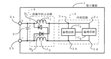
図1は本発明にかかる誤動作防止回路の一実施例を備えた電子機器の回路図である。
【0032】
本実施例における誤動作防止回路4は、電子機器1の正極電源端子2aと内部回路3の正極入力端子3aとの間に接続される第1のインダクタンス素子L1と、電子機器の負極電源端子2bと、内部回路3の負極入力端子3bとの間に接続される第2のインダクタンス素子L2と、正極電源端子2aから負極入力端子3bへ電流が流れるのを阻止するように接続された第1の整流素子D1と、負極入力端子3bから正極電源端子2aへ電流が流れるのを阻止するように接続された第2の整流素子D2とにより構成される。
【0033】
本実施例においては、第1および第2のインダクタンス素子L1、L2には、例えば容量1μHのコイルを用い、第1及び第2の整流素子D1、D2にはショットキ・ダイオードを用いている。
【0034】
次に、上記構成を有する本発明にかかる誤動作防止回路4の実施例の動作について説明する。
【0035】
図3は、本発明にかかる誤動作防止回路4を備えた電子機器1と、この誤動作防止回路4の動作を試験するシミュレータ5の回路図である。
【0036】
電子機器1の電源端子2a、2bに静電気を放電するためにシミュレータ5を用いる。このシミュレータ5は、高電圧発生装置6と、充電用スイッチSW1と、コンデンサCと、放電用スイッチSW2と、放電用プローブ7とで構成される。
【0037】
まず、スイッチSW2を開放し、スイッチSW1を閉じて、コンデンサCに高電圧発生装置6から充電する。次にスイッチSW1を開放し、スイッチSW2を閉じてコンデンサCに蓄まった電荷を放電用プローブ7から電源端子2aに放電させる。この時の電圧は1kV乃至8kVであって、コンデンサCの容量は10pFを用いた。
【0038】
スイッチSW2を閉じて放電させた後長時間経過すると、放電された電荷は電子機器1へ略々平均的に分布することになるが、放電直後は過渡現象により、回路内で異常な電位の変化が現れる。
【0039】
本発明では、内部回路3の電源電位に注目した時の異常な電位差を電源2の電圧が上がる方向へ整流するようにした。
ここで、電荷を放電する時の電荷の極性と放電する端子の組み合わせは以下の(1)乃至(4)の4通りある。この動作を図1及び図2を参照しながら説明する。
【0040】
(1)正極電源端子2aに正電荷を放電すると、正電荷はすべて第1のインダクタンス素子L1を通って正極入力端子3aに流れ込む。尚、整流素子D1が存在するため、正電荷が負極入力端子3bに流れ込むことはない。従って、図2(a)に示すように、正極入力端子3aの電圧は急激に上昇するが、すぐに元の値に戻る。この電圧の上昇は、論理判定基準電圧を大きく超える方向に作用するから、論理判定を間違えることはなく、電子機器1の誤動作は起こらない。
【0041】
(2)正極電源端子2aに負電荷を放電すると、負電荷の大部分は整流素子D1を通って負極入力端子3bに流れる。また、負電荷の残りの一部は第1のインダクタンス素子L1を通過するが、第1のインダクタンス素子L1のインピーダンスにより、通過する電荷量は極めて少ない。さらに、通過した電荷の一部は整流素子D2を通って負極電源端子2bに戻るので、正極入力端子3aに流入する負電荷は極めて少なく、正極入力端子3aの電圧降下は僅かである。また、負電荷の大部分は負極入力端子3bに流れ込むため、図2(b)に示すように、負極入力端子3bの電圧を大きく低下させる。これによって、正極入力端子3aと負極入力端子3bとの間の電位差が大きくなるので、この電位差が論理判定基準電圧を下回ることはなく、電子機器1の誤動作は起こらない。
【0042】
(3)負極電源端子2bに正電荷を放電すると、正電荷の大部分は整流素子D2を通って正極入力端子3aに流れ込み、図2(c)に示すように、正極入力端子3aの電圧を上昇させる。第2のインダクタンス素子L2のインピーダンスにより第2のインダクタンス素子L2を通って負極入力端子3bに流入する正電荷は極めて少なく、負極入力端子3bの電圧上昇は僅かである。従って、図2(a)の場合と同様に、正極入力端子3aと負極入力端子3bとの間の電位差を大きくするため、電子機器1の誤動作は起こらない。
【0043】
(4)負極電源端子2bに負電荷を放電すると、負電荷はすべて第2のインダクタンス素子L2を通って負極入力端子3bに流れ、負電荷が正極入力端子3aに流れ込むことはない。従って、図2(d)に示すように、負極入力端子3bの電圧は大きく低下し、正極入力端子3aとの間の電位差が大きくなるため、誤動作は起こらない。
【0044】
以上説明したように、本発明の誤動作防止回路では、正負の電源端子2a、2bのいずれに正電荷または負電荷が飛び込んで来ても、正電荷は正極入力端子3aに流れるように、負電荷は負極入力端子3bに流れるように構成したので、論理判定を間違えることがなく、電子機器1の誤動作を防止することができる。
【0045】
また、本発明では、正電荷を回路の耐圧が高い方向へ整流しているため、第1従来例のようにインダクタンス素子のみを用いる場合に比べ静電気に対する耐圧を上げることができる。
【0046】
さらにまた、第2従来例のように、全波整流ブリッジ回路を用いた場合、ショットキ・ダイオードを通過させると0.3V程度の電圧降下が発生するが、本発明では、整流素子(ダイオード)D3、D4をインダクタンス素子L1、L2に置換しているので、通常動作時の電圧降下が低減されている。
【0047】
【発明の効果】
請求項1記載の発明によれば、電子機器の電源端子と内部回路との間にインダクタンス素子と整流素子とで構成される誤動作防止回路を設け、正負の電源端子のいずれに正電荷または負電荷が飛び込んで来ても、正電荷は内部回路の正極入力端子に流し、負電荷は内部回路の負極入力端子に流れるようにしたので、静電荷の飛び込みがあっても、内部回路の正または負極入力端子の電圧が論理判定条件を超えて誤った論理判定を行うことがなく、静電気による電子機器の誤動作を防止することができる。
【0048】
また、請求項1記載の発明によれば、インダクタンス素子のみを用いた従来品に比べて、静電気に対する耐圧を上げることができる。
さらに、請求項1記載の発明によれば、全波整流ブリッジ回路を用いた従来品に比べて、通常動作時の誤動作防止回路による電圧降下を小さくすることができる。
【図面の簡単な説明】
【図1】本発明にかかる誤動作防止回路の一実施例を備えた電子機器の回路図である。
【図2】本発明にかかる誤動作防止回路の一実施例の動作を説明するための電圧波形図である。
【図3】本発明にかかる誤動作防止回路を備えた電子機器と、この誤動作防止回路の動作を試験するためのシミュレータの回路図である。
【図4】誤動作防止回路を備えた電子機器の第1従来例の回路図である。
【図5】誤動作防止回路を備えた電子機器の第2従来例の回路図である。
【図6】誤動作防止回路の第1従来例の動作を説明するための電圧波形図である。
【図7】誤動作防止回路の第2従来例の動作を説明するための電圧波形図である。
【符号の説明】
1 電子機器
2 電源
2a 正極電源端子
2b 負極電源端子
3 内部回路
3a 正極入力端子
3b 負極入力端子
4 誤動作防止回路
5 シミュレータ
6 高電圧発生装置
7 プローブ
D1、D2 整流素子
L1、L2 インダクタンス素子[0001]
BACKGROUND OF THE INVENTION
The present invention relates to a malfunction prevention circuit, and more particularly to a malfunction prevention circuit that prevents an electronic device having a logic circuit therein, such as a mobile phone, from malfunctioning due to static electricity.
[0002]
[Prior art]
An electronic device that has a logic circuit inside and operates digitally, such as a mobile phone, is made of an insulating material such as plastic. Since the electronic equipment sometimes malfunctions due to this static electricity, various countermeasures have been taken.
[0003]
FIG. 4 is a circuit diagram of a first example of an electronic apparatus provided with a conventional malfunction prevention circuit. This electronic device has a
[0004]
The malfunction prevention circuit 11 includes a first inductance element L1 connected between the positive power supply terminal 2a and the positive input terminal 3a of the
[0005]
The operation of the malfunction prevention circuit 11 will be described with reference to FIGS.
When a positive charge jumps into the positive power supply terminal 2a, the positive charge flows into the positive input terminal 3a of the
[0006]
On the other hand, when a negative charge jumps into the positive power supply terminal 2a, the negative charge flows into the positive input terminal 3a through the first inductance element L1. At this time, as shown in FIG. 6B, the voltage of the positive electrode input terminal 3a drops rapidly but immediately returns to the original value. Due to this sudden voltage drop, the voltage at the positive input terminal 3a may drop below the logic determination reference voltage, which may cause malfunction.
[0007]
Further, when a positive charge jumps into the negative power supply terminal 2b, the positive charge flows into the negative input terminal 3b through the second inductance element L2, and raises the voltage of the negative input terminal 3b. This means that when the positive input terminal 3a is viewed with reference to the negative input terminal 3b, the voltage of the positive input terminal 3a is low, and the same phenomenon as shown in FIG. 6B occurs. It will be. Accordingly, malfunction occurs when the potential difference between the positive input terminal 3a and the negative input terminal 3b becomes smaller than the logic determination reference voltage.
[0008]
Further, when negative charge jumps into the negative power supply terminal 2b, the negative charge flows into the negative input terminal 3b through the second inductance element L2, and decreases the voltage at the negative input terminal 3b. When the positive input terminal 3a is viewed with reference to the negative input terminal 3b, the voltage of the positive input terminal 3a rises, and the same phenomenon as shown in FIG. Become. Therefore, the potential difference between the positive input terminal 3a and the negative input terminal 3b becomes larger than the logic determination reference voltage, and no malfunction occurs.
[0009]
FIG. 5 is a circuit diagram of a second example of an electronic apparatus provided with a conventional malfunction prevention circuit. This malfunction prevention circuit 12 is composed of four rectifying elements D1 to D4 assembled in a full-wave rectification type bridge circuit, and between the power supply terminals 2a and 2b and the input terminals 3a and 3b of the
[0010]
The operation of the malfunction prevention circuit 12 will be described with reference to FIGS.
When positive charge jumps into the positive power supply terminal 2a, the positive charge passes through the rectifying element D3 and temporarily increases the voltage of the positive input terminal 3a as shown in FIG. 7A. Return to value. This is a direction in which the potential difference between the positive input terminal 3a and the negative input terminal 3b is increased, so this potential difference does not become lower than the logic determination reference voltage, and no malfunction occurs.
[0011]
On the other hand, when a negative charge jumps into the positive power supply terminal 2a, the negative charge flows into the negative input terminal 3b through the rectifying element D1, and the voltage at the negative input terminal 3b is changed as shown in FIG. Lower. This is a direction in which the potential difference between the positive electrode input terminal 3a and the negative electrode input terminal 3b is increased. Therefore, this potential difference does not become lower than the logic determination reference voltage, and no malfunction occurs.
[0012]
When positive charge jumps into the negative power supply terminal 2a, the positive charge passes through the rectifying element D2 and is input to the positive input terminal 3a. As shown in FIG. Raise. In this case, no malfunction occurs for the same reason as described in FIG.
[0013]
Further, when a negative charge jumps into the negative power supply terminal 2a, the negative charge flows into the negative input terminal 3b through the rectifying element D4, and the voltage at the negative input terminal 3b is changed as shown in FIG. Reduce. In this case, no malfunction occurs for the same reason as described in FIG.
[0014]
As is apparent from the above description, in the malfunction prevention circuit 12 in which the four rectifying elements D1 to D4 are assembled in a full-wave rectification bridge circuit, a positive charge or a negative charge jumps into any of the positive and negative power supply terminals 2a and 2b. However, since the positive charge always flows into the positive input terminal 3a and the negative charge flows into the negative input terminal 3b, the potential difference between the positive input terminal 3a and the negative input terminal 3b is never lower than the logic determination reference voltage. It is possible to prevent malfunction of the electronic device.
[0015]
[Problems to be solved by the invention]
However, in the conventional malfunction prevention circuit, the following problems remain unsolved.
That is, in the case of the first conventional example, when static electricity jumps into the power supply terminal, the circuit passes through the inductance elements L1 and L2 from the terminal where all the charge jumps, whether it is a positive charge or a negative charge. Flows to the side. The case where the charge is positive and the case where the charge is negative will be described below.
(1) Consider a case where positive charge enters from the positive power supply terminal. Since positive charges come in, the potential of the positive power supply terminal 2a temporarily rises. Accordingly, the potential of the positive input terminal 3a of the
[0017]
(2) Next, consider a case where negative charges enter from the positive power supply terminal 2a. Since negative charges come in, the potential of the positive power supply terminal 2a temporarily drops. Accordingly, the potential of the positive input terminal 3a of the
[0018]
Comparing these two states, when the same amount of charge (voltage) is applied, the latter is less susceptible to malfunction than the former. This is because the value held by the logic circuit decreases from the logic determination level as the power supply voltage decreases, causing the electronic device to malfunction.
[0019]
In an integrated circuit, a malfunction margin with respect to noise at a power supply terminal is generally more likely to malfunction due to a negative change than a positive change in power supply voltage. Similarly, the ground-side power supply terminal is more likely to malfunction when the change is positive than when it is negative.
[0020]
I will explain this in more detail. Hereinafter, in order to facilitate understanding, a case where two logic circuits of the
(1) The power supply voltage of one logic circuit varies, and the other power supply voltage does not vary.
(2) On the ground side, there is no potential difference between logic circuits.
(3) The logic element is a C-MOS, and the output voltage is Vcc at the high level H and 0 V at the low level L.
[0021]
First, consider a case where a positive charge is applied to the positive input terminal 3a of the logic circuit IC1 on the output side. At this time, it is assumed that a voltage of Vcc + ΔV is applied to the positive input terminal 3a of the logic circuit IC1. The output voltage at that time is Vcc + ΔV. At this time, the logic judgment level in the receiving side logic circuit IC2 is Vcc / 2.
Vcc + ΔV> Vcc / 2
Therefore, there is no mistake in logic judgment.
[0022]
Next, when a negative charge is applied to the positive input terminal 3a of the output side logic circuit IC1, it is assumed that a voltage of Vcc−ΔV is applied to the positive input terminal 3a of the logic circuit IC1. The output voltage at that time is Vcc−ΔV. At this time, the logic judgment level in the receiving side logic circuit IC2 is Vcc / 2.
Vcc-ΔV> Vcc / 2
Voltage that does not satisfy
ΔV> Vcc / 2
Incorrect logic judgment.
[0023]
Next, when a positive charge is applied to the positive input terminal 3a of the logic circuit IC2 on the receiving side, a voltage of Vcc + ΔV is applied to the positive input terminal 3c of the logic circuit IC2. At this time, since the logic judgment level in the receiving side logic circuit IC2 is (Vcc + ΔV) / 2,
Vcc> (Vcc + ΔV) / 2
Voltage that does not satisfy
ΔV> Vcc
Incorrect logic judgment.
[0024]
Finally, when a negative charge is applied to the positive input terminal 3c of the logic circuit IC2 on the receiving side, a voltage of Vcc−ΔV is applied to the positive input terminal 3c of the logic circuit IC2. At this time, the logic judgment level in the receiving side logic circuit IC2 is (Vcc−ΔV) / 2.
Vcc> (Vcc−ΔV) / 2
Voltage that does not satisfy
ΔV> Vcc
Incorrect logic judgment.
Thus, it can be said that ΔV <Vcc / 2 is the limit of operation.
[0025]
On the other hand, in the case of the second conventional example, the electric charge is rectified and flows to the
However, since the voltage drop in the malfunction prevention circuit 12 is large, there is a problem that it is disadvantageous for a battery-operated device such as a cellular phone.
[0026]
Accordingly, the present invention has been made in view of the above-described conventional problems, and provides a malfunction prevention circuit that is less likely to malfunction even when positive and negative positive charges are input to a power supply terminal and that has a small voltage drop. With the goal.
[0027]
[Means for Solving the Problems]
The invention according to
[0028]
According to the first aspect of the present invention, the first and second rectifying elements are inserted between the power source and the logic circuit so that the current flows in the forward direction. Regardless of which positive charge or negative charge jumps in, positive charge flows to the positive input terminal, negative charge flows to the negative input terminal, and the first and second inductance elements are inserted. Therefore, it is possible to suppress a sudden flow of charges into the logic circuit, and malfunctions are less likely to occur regardless of whether positive charges or negative charges are input to the power supply terminal.
[0029]
In addition, according to the first aspect of the present invention, since only half of the rectifying element of the conventional full-wave rectifying bridge circuit is used, the voltage drop due to the rectifying element can be reduced.
[0030]
Furthermore, according to the first aspect of the present invention, the inductance element acts as an inductance element only when a positive charge jumps in, and performs an impedance action to suppress a rapid flow of the positive charge. Since a direct current flows, there is no inductance effect and the voltage drop is only the resistance component, but the resistance component of the inductance element is extremely small, and the voltage drop due to the resistance component is negligible.
[0031]
DETAILED DESCRIPTION OF THE INVENTION
Next, specific examples of embodiments of the malfunction prevention circuit according to the present invention will be described with reference to the drawings.
FIG. 1 is a circuit diagram of an electronic apparatus provided with an embodiment of a malfunction prevention circuit according to the present invention.
[0032]
The malfunction prevention circuit 4 in this embodiment includes a first inductance element L1 connected between the positive power supply terminal 2a of the
[0033]
In this embodiment, coils having a capacitance of 1 μH, for example, are used for the first and second inductance elements L1, L2, and Schottky diodes are used for the first and second rectifier elements D1, D2.
[0034]
Next, the operation of the embodiment of the malfunction prevention circuit 4 according to the present invention having the above configuration will be described.
[0035]
FIG. 3 is a circuit diagram of the
[0036]
A
[0037]
First, the switch SW2 is opened, the switch SW1 is closed, and the capacitor C is charged from the high voltage generator 6. Next, the switch SW1 is opened, the switch SW2 is closed, and the electric charge stored in the capacitor C is discharged from the discharge probe 7 to the power supply terminal 2a. The voltage at this time is 1 kV to 8 kV, and the capacitance of the capacitor C is 10 pF.
[0038]
When the switch SW2 is closed and discharged for a long time, the discharged electric charge is distributed almost averagely to the
[0039]
In the present invention, the abnormal potential difference when attention is paid to the power supply potential of the
Here, there are the following four combinations (1) to (4) of the charge polarity and the discharge terminal when discharging the charge. This operation will be described with reference to FIGS.
[0040]
(1) When positive charge is discharged to the positive power supply terminal 2a, all positive charge flows into the positive input terminal 3a through the first inductance element L1. In addition, since the rectifying element D1 exists, the positive charge does not flow into the negative input terminal 3b. Accordingly, as shown in FIG. 2A, the voltage of the positive input terminal 3a rapidly increases, but immediately returns to the original value. This increase in voltage acts in a direction that greatly exceeds the logic determination reference voltage, so that the logic determination is not mistaken and the
[0041]
(2) When negative charge is discharged to the positive power supply terminal 2a, most of the negative charge flows to the negative input terminal 3b through the rectifying element D1. Further, the remaining part of the negative charge passes through the first inductance element L1, but the amount of charge passing therethrough is very small due to the impedance of the first inductance element L1. Furthermore, since a part of the passed charge passes through the rectifying element D2 and returns to the negative power supply terminal 2b, the negative charge flowing into the positive input terminal 3a is very small, and the voltage drop at the positive input terminal 3a is slight. Further, since most of the negative charge flows into the negative input terminal 3b, as shown in FIG. 2B, the voltage of the negative input terminal 3b is greatly reduced. As a result, the potential difference between the positive input terminal 3a and the negative input terminal 3b increases, so that the potential difference does not fall below the logic determination reference voltage, and the
[0042]
(3) When a positive charge is discharged to the negative power supply terminal 2b, most of the positive charge flows into the positive input terminal 3a through the rectifying element D2, and as shown in FIG. Raise. The positive charge flowing into the negative input terminal 3b through the second inductance element L2 due to the impedance of the second inductance element L2 is extremely small, and the voltage rise at the negative input terminal 3b is slight. Accordingly, as in the case of FIG. 2A, the potential difference between the positive electrode input terminal 3a and the negative electrode input terminal 3b is increased, so that the
[0043]
(4) When the negative charge is discharged to the negative power supply terminal 2b, all the negative charge flows through the second inductance element L2 to the negative input terminal 3b, and no negative charge flows into the positive input terminal 3a. Accordingly, as shown in FIG. 2D, the voltage at the negative input terminal 3b is greatly reduced, and the potential difference with the positive input terminal 3a is increased, so that no malfunction occurs.
[0044]
As described above, in the malfunction prevention circuit of the present invention, the positive charge or the negative charge jumps into any of the positive and negative power supply terminals 2a and 2b, so that the positive charge flows to the positive input terminal 3a. Is configured to flow to the negative electrode input terminal 3b, so that the logic determination is not mistaken and the malfunction of the
[0045]
In the present invention, since the positive charge is rectified in the direction in which the withstand voltage of the circuit is higher, the withstand voltage against static electricity can be increased as compared with the case where only the inductance element is used as in the first conventional example.
[0046]
Further, when a full-wave rectifier bridge circuit is used as in the second conventional example, a voltage drop of about 0.3 V occurs when the Schottky diode is passed. In the present invention, the rectifier element (diode) D3 , D4 is replaced with inductance elements L1 and L2, so that the voltage drop during normal operation is reduced.
[0047]
【The invention's effect】
According to the first aspect of the present invention, the malfunction prevention circuit composed of the inductance element and the rectifying element is provided between the power supply terminal of the electronic device and the internal circuit, and either the positive or negative power supply terminal has a positive charge or a negative charge. The positive charge flows to the positive input terminal of the internal circuit and the negative charge flows to the negative input terminal of the internal circuit. The input terminal voltage does not exceed the logic determination condition and erroneous logic determination is not performed, and malfunction of the electronic device due to static electricity can be prevented.
[0048]
In addition, according to the first aspect of the present invention, the withstand voltage against static electricity can be increased as compared with the conventional product using only the inductance element.
Furthermore, according to the first aspect of the present invention, the voltage drop caused by the malfunction prevention circuit during normal operation can be reduced as compared with the conventional product using the full-wave rectification bridge circuit.
[Brief description of the drawings]
FIG. 1 is a circuit diagram of an electronic apparatus provided with an embodiment of a malfunction prevention circuit according to the present invention.
FIG. 2 is a voltage waveform diagram for explaining the operation of one embodiment of the malfunction prevention circuit according to the present invention.
FIG. 3 is a circuit diagram of an electronic device including a malfunction prevention circuit according to the present invention and a simulator for testing the operation of the malfunction prevention circuit.
FIG. 4 is a circuit diagram of a first conventional example of an electronic device provided with a malfunction prevention circuit.
FIG. 5 is a circuit diagram of a second conventional example of an electronic apparatus provided with a malfunction prevention circuit.
FIG. 6 is a voltage waveform diagram for explaining the operation of the first conventional example of the malfunction prevention circuit.
FIG. 7 is a voltage waveform diagram for explaining the operation of the second conventional example of the malfunction prevention circuit.
[Explanation of symbols]
DESCRIPTION OF
Claims (1)
前記電子機器の正極電源端子と前記論理回路の正極入力端子との間に接続される第1のインダクタンス素子と、
前記電子機器の負極電源端子と前記論理回路の負極入力端子との間に接続される第2のインダクタンス素子と、
前記正極電源端子から前記負極入力端子へ電流が流れるのを阻止するように接続された第1の整流素子と、
前記正極入力端子から前記負極電源端子へ電流が流れるのを阻止するように接続された第2の整流素子とを備えたことを特徴とする誤動作防止回路。 A malfunction prevention circuit for preventing malfunction of an electronic device provided therein with a logic circuit for logically judging according to a predetermined judgment reference voltage,
A first inductance element connected between a positive power supply terminal of the electronic device and a positive input terminal of the logic circuit;
A second inductance element connected between a negative power supply terminal of the electronic device and a negative input terminal of the logic circuit;
A first rectifier element connected to prevent current from flowing from the positive power supply terminal to the negative input terminal;
A malfunction prevention circuit, comprising: a second rectifier element connected to prevent current from flowing from the positive input terminal to the negative power supply terminal.
Priority Applications (1)
| Application Number | Priority Date | Filing Date | Title |
|---|---|---|---|
| JP34224097A JP4143152B2 (en) | 1997-11-27 | 1997-11-27 | Malfunction prevention circuit |
Applications Claiming Priority (1)
| Application Number | Priority Date | Filing Date | Title |
|---|---|---|---|
| JP34224097A JP4143152B2 (en) | 1997-11-27 | 1997-11-27 | Malfunction prevention circuit |
Publications (2)
| Publication Number | Publication Date |
|---|---|
| JPH11162693A JPH11162693A (en) | 1999-06-18 |
| JP4143152B2 true JP4143152B2 (en) | 2008-09-03 |
Family
ID=18352202
Family Applications (1)
| Application Number | Title | Priority Date | Filing Date |
|---|---|---|---|
| JP34224097A Expired - Fee Related JP4143152B2 (en) | 1997-11-27 | 1997-11-27 | Malfunction prevention circuit |
Country Status (1)
| Country | Link |
|---|---|
| JP (1) | JP4143152B2 (en) |
-
1997
- 1997-11-27 JP JP34224097A patent/JP4143152B2/en not_active Expired - Fee Related
Also Published As
| Publication number | Publication date |
|---|---|
| JPH11162693A (en) | 1999-06-18 |
Similar Documents
| Publication | Publication Date | Title |
|---|---|---|
| JP3905005B2 (en) | Portable device and semiconductor integrated circuit device | |
| US6642694B2 (en) | Overcharge protection circuit capable of preventing damage to a charge control switch on flowing an excessive current | |
| EP0123030A1 (en) | Isolated power supply feedback | |
| US20070030714A1 (en) | Enabling Circuit for Avoiding Negative Voltage Transients | |
| WO1996009676A1 (en) | Transient voltage protection circuit for electrical power converters | |
| US4970451A (en) | Device for utilizing low voltage electric current sources | |
| US6356468B1 (en) | Arrangement for limiting starting current in a power supply | |
| CN111049203A (en) | Charge and discharge management circuit and chargeable electronic equipment | |
| EP0663712B1 (en) | Earth leakage breaker and earth leakage-current protection system | |
| US8508892B2 (en) | Integrated circuit with DC-DC converter and ESD protection | |
| JP4143152B2 (en) | Malfunction prevention circuit | |
| DE69925984T2 (en) | Battery charger | |
| WO2005122372A1 (en) | Method and circuit arrangement for optimising maximum current limitation in the primary switch of a switched-mode power supply, and a power supply | |
| JP2003079058A (en) | Battery pack | |
| JP3658597B2 (en) | Surge protector | |
| JPS6098722A (en) | Electronic switch | |
| US20240266159A1 (en) | Power Supply Device for Triple Quadrupole Mass Spectrometer | |
| JP3642105B2 (en) | Battery pack | |
| JP2952315B2 (en) | Storage battery device | |
| JP3821249B2 (en) | Earth leakage breaker | |
| KR920009361B1 (en) | Charge / discharge control circuit | |
| JP2841470B2 (en) | Charge / discharge circuit | |
| JP2825874B2 (en) | Battery charging / discharging circuit for power supply unit | |
| JP3521510B2 (en) | DC-DC converter circuit | |
| JPS60183938A (en) | Dc power source |
Legal Events
| Date | Code | Title | Description |
|---|---|---|---|
| A621 | Written request for application examination |
Free format text: JAPANESE INTERMEDIATE CODE: A621 Effective date: 20041005 |
|
| A977 | Report on retrieval |
Free format text: JAPANESE INTERMEDIATE CODE: A971007 Effective date: 20080124 |
|
| A131 | Notification of reasons for refusal |
Free format text: JAPANESE INTERMEDIATE CODE: A131 Effective date: 20080128 |
|
| A521 | Written amendment |
Free format text: JAPANESE INTERMEDIATE CODE: A523 Effective date: 20080311 |
|
| TRDD | Decision of grant or rejection written | ||
| A01 | Written decision to grant a patent or to grant a registration (utility model) |
Free format text: JAPANESE INTERMEDIATE CODE: A01 Effective date: 20080602 |
|
| A01 | Written decision to grant a patent or to grant a registration (utility model) |
Free format text: JAPANESE INTERMEDIATE CODE: A01 |
|
| A61 | First payment of annual fees (during grant procedure) |
Free format text: JAPANESE INTERMEDIATE CODE: A61 Effective date: 20080616 |
|
| FPAY | Renewal fee payment (event date is renewal date of database) |
Free format text: PAYMENT UNTIL: 20110620 Year of fee payment: 3 |
|
| R150 | Certificate of patent or registration of utility model |
Free format text: JAPANESE INTERMEDIATE CODE: R150 |
|
| FPAY | Renewal fee payment (event date is renewal date of database) |
Free format text: PAYMENT UNTIL: 20120620 Year of fee payment: 4 |
|
| FPAY | Renewal fee payment (event date is renewal date of database) |
Free format text: PAYMENT UNTIL: 20120620 Year of fee payment: 4 |
|
| FPAY | Renewal fee payment (event date is renewal date of database) |
Free format text: PAYMENT UNTIL: 20130620 Year of fee payment: 5 |
|
| LAPS | Cancellation because of no payment of annual fees |