JP4053173B2 - Microwave plasma processing apparatus and method - Google Patents
Microwave plasma processing apparatus and method Download PDFInfo
- Publication number
- JP4053173B2 JP4053173B2 JP08567599A JP8567599A JP4053173B2 JP 4053173 B2 JP4053173 B2 JP 4053173B2 JP 08567599 A JP08567599 A JP 08567599A JP 8567599 A JP8567599 A JP 8567599A JP 4053173 B2 JP4053173 B2 JP 4053173B2
- Authority
- JP
- Japan
- Prior art keywords
- temperature
- slot electrode
- microwave
- temperature control
- wavelength shortening
- Prior art date
- Legal status (The legal status is an assumption and is not a legal conclusion. Google has not performed a legal analysis and makes no representation as to the accuracy of the status listed.)
- Expired - Fee Related
Links
Images


Classifications
-
- H10P72/0602—
-
- H—ELECTRICITY
- H01—ELECTRIC ELEMENTS
- H01J—ELECTRIC DISCHARGE TUBES OR DISCHARGE LAMPS
- H01J37/00—Discharge tubes with provision for introducing objects or material to be exposed to the discharge, e.g. for the purpose of examination or processing thereof
- H01J37/32—Gas-filled discharge tubes
- H01J37/32009—Arrangements for generation of plasma specially adapted for examination or treatment of objects, e.g. plasma sources
- H01J37/32192—Microwave generated discharge
-
- H10P72/0421—
Landscapes
- Physics & Mathematics (AREA)
- Engineering & Computer Science (AREA)
- Plasma & Fusion (AREA)
- Chemical & Material Sciences (AREA)
- Analytical Chemistry (AREA)
- Plasma Technology (AREA)
- Physical Or Chemical Processes And Apparatus (AREA)
- Chemical Vapour Deposition (AREA)
- ing And Chemical Polishing (AREA)
Description
【0001】
【0002】
【発明の属する技術分野】
本発明は、マイクロ波プラズマ処理装置及び方法に関する。
【0003】
【従来の技術】
近年、半導体製品の高密度化及び高微細化に伴い、半導体製品の製造工程において、成膜、エッチング、アッシング等の処理のためにプラズマ処理装置が使用される場合がある。特に、0.1乃至10mTorr程度の減圧状態でも安定してプラズマを立てることができることからマイクロ波とリング状コイルからの磁場を組合せて高密度プラズマを発生させるマイクロ波プラズマ装置が提案されている。
【0004】
典型的なマイクロ波プラズマ装置においては、例えば、2.45GHz程度のマイクロ波が、導波管、透過窓、スロット電極を順に通過し、被処理体が配置され減圧環境下に維持された処理室内に導入される。一方、反応ガスも処理室に導入され、マイクロ波によってプラズマ化され、活性の強いラジカルとイオンとなり、これが被処理体と反応してエッチングなどが行われる。
【0005】
マイクロ波は、スロット電極に導入される前にその波長を短縮する誘電体(以下、「波長短縮部材」という。)を通過される場合もある。これにより、マイクロ波の波長が短くなるのでスロット電極に形成されるスリットの間隔を短くすることができる。波長短縮部材については、例えば、本出願人により既に出願されている特開平9−63793号に開示されている。
【0006】
さて、透過窓は石英やアルミナなどによって形成されるがプラズマ熱によって加熱されて損傷したり脆弱になる。また、波長短縮部材やスロット電極もプラズマ熱により熱膨張する。例えば、スロット電極は銅板などにより形成されるが、熱膨張により最適なスリット長さが変化して処理室内における全体のプラズマ密度が低下したり部分的にプラズマ密度が集中したりする。全体のプラズマ密度が低下すれば半導体ウェハの処理速度が変化する。その結果、プラズマ処理が時間的に管理される場合、所定の時間(例えば、2分)で処理を停止しても所望の処理(エッチング深さや成膜厚さ)が半導体ウェハに形成されていない場合がある。また、部分的にプラズマ密度が集中すれば、部分的に半導体ウェハの処理が変化してしまう。
【0007】
かかる問題を解決するために、例えば、特開平3−191073号は、冷却水を使用した冷却手段を設けて透過窓を冷却するマイクロ波プラズマ処理装置を提案している。また、上述の特開平9−63793号は、波長短縮部材とスロット電極の覆い部材に冷却ジャケットを設けることを提案している(段落番号【0008】参照)。
【0009】
【発明が解決しようとする課題】
しかし、プラズマCVD装置においては、水分が液状又は霧状として残っていると半導体ウェハに形成される膜中に不純物として入り込むため、処理室の温度はできるだけ上げることが好ましい。しかるに、特開平3−191073号のように単純に冷却手段を設けるだけではプラズマ処理の品質が低下してしまう。このように、従来は、被処理体の品質を維持しつつプラズマ熱の弊害を除去することができなかった。
【0010】
また、処理室と誘電体とを接合するオーリングなど高温に対しての耐性が弱い部材については一定温度以上の温度がかからないように制御する必要がある。もう一つの課題として、特開平9−63793号には波長短縮部材にどのような材質を用いるかは開示されておらずその材質を考慮しないと熱伝導がしにくくなる。そのため、温度制御がしずらくなり処理の均一性が悪くなる。
【0011】
そこで、このような課題を解決する新規かつ有用な減圧環境内で動作可能なマイクロ波プラズマ処理装置及び方法を提供することを本発明の概括的目的とする。
【0012】
【課題を解決するための手段】
本発明の例示的一態様であるマイクロ波処理装置は、マイクロ波が導入されると当該マイクロ波の波長を短縮する波長短縮部材と、当該波長短縮部材に接続され、前記波長短縮部材を通過した前記マイクロ波を案内するスロット電極と、前記波長短縮部材及び前記スロット電極の温度を制御することができる第1の温度制御装置と、反応ガスを供給する反応ガス源及び真空ポンプに接続可能で被処理体を収納することができ、前記スロット電極を通過した前記マイクロ波と前記反応ガスが供給されると、減圧環境下で前記被処理体に所定の処理を施すことができる処理室とを有する。前記第1の温度制御装置は、前記処理室内に水分が付着するのを抑制する温度に前記スロット電極を制御してもよい。また、前記第1の温度制御装置は、前記スロット電極の前記温度を70℃±10℃に制御してもよい。また、前記第1の温度制御装置は前記波長短縮部材及び前記スロット電極のいずれか一方の温度を制御し、当該いずれか一方の熱伝導率を利用して他方の温度も制御することができる。
【0013】
前記マイクロ波プラズマ処理装置は、前記波長短縮部材を収納すると共に前記スロット電極に接続されたアンテナ収納部材を更に有し、前記第1の温度制御装置は、前記アンテナ収納部材の温度を制御することによって、前記アンテナ収納部材の熱伝導率を利用して前記波長短縮部材及び前記スロット電極の温度を制御することができる。前記マイクロ波プラズマ処理装置は、前記スロット電極と前記処理室との間に配置された誘電体を更に有し、前記第1の温度制御装置は前記波長短縮部材、前記スロット電極及び前記誘電体の一つの温度を制御し、当該一つの熱伝導率を利用して前記スロット電極の温度も制御することができる。更に、前記マイクロ波プラズマ装置は、前記被処理体の温度が所定の処理温度になるように制御する第2の温度制御装置又は前記プラズマ装置前記誘電体の周辺を温度制御する第3の温度制御装置を更に有することができる。
【0014】
本発明の例示的一態様であるプラズマ処理方法は、被処理体を処理室に収納する工程と、前記処理室内の圧力を制御する工程と、スロット電極の温度を制御する工程と、反応ガスを前記処理室内に導入する工程と、マイクロ波を前記スロット電極に供給する工程と、前記マイクロ波によるプラズマで前記被処理体を処理する工程とを有する。前記温度制御工程は、マイクロ波の波長を短縮するように動作可能な波長短縮部材を温度制御する工程と、前記温度制御された波長短縮部材から前記スロット電極への熱伝導のみを利用して前記スロット電極を温度制御する工程とから構成されてもよい。
【0015】
本発明の別の例示的態様であるプラズマ処理方法は、被処理体を処理室に収納する工程と、前記処理室内の圧力を制御する工程と、スロット電極の温度を制御する工程と、反応ガスを前記処理室内に導入する工程と、前記スロット電極が所定温度以下になったときにマイクロ波を前記スロット電極に供給する工程と、前記マイクロ波によるプラズマで前記被処理体を処理する工程とを有する。前記温度制御工程は、マイクロ波の波長を短縮するように動作可能な波長短縮部材を所定の温度以下に温度制御する工程と、前記温度制御された波長短縮部材から前記スロット電極への熱伝導のみを利用して前記スロット電極を温度制御する工程とから構成されてもよい。
【0016】
なお上述のいずれのプラズマ処理方法においても、前記温度制御工程は、前記スロット電極に接続された誘電体を温度制御する工程と、前記温度制御された誘電体から前記スロット電極への熱伝導のみを利用して前記スロット電極を温度制御する工程とから構成されてもよく、また、前記被処理体を温度制御する工程を更に有してもよい。
【0017】
【発明の実施の形態】
以下、添付図面を参照して、プラズマCVD装置として使用される本発明の例示的なマイクロ波プラズマ装置100について説明する。なお、各図において同一の参照符号は同一部材を表している。従来のマイクロ波は1〜100GHzの周波数をいうが、本発明のマイクロ波はこれに限らず、およそ50MHz〜100GHzのものをいう。ここで、図1は、マイクロ波プラズマ装置100の概略ブロック図である。本実施例のマイクロ波プラズマ装置100は、マイクロ波源10と反応ガス供給ノズル50と真空ポンプ60とに接続され、アンテナ収納部材20と、第1の温度制御装置30と、処理室40と、第2の温度制御装置70とを有している。
【0018】
マイクロ波源10は、例えば、マグネトロンからなり、通常2.45GHzのマイクロ波(例えば、5kW)を発生することができる。マイクロ波は、その後、図示しないモード変換器により伝送形態がTM、TE又はTEMモードなどに変換される。なお、図1では、発生したマイクロ波がマグネトロンへ戻る反射波を吸収するアイソレータや、負荷側とのマッチングをとるためのEHチューナ又はスタブチューナは省略されている。
【0019】
アンテナ収納部材20には波長短縮部材22が収納され、波長短縮部材22に接触してスロット電極24がアンテナ収納部材20の底板として構成されている。アンテナ収納部材20には熱伝導率が高い材料(例えば、ステンレス)が使用されており、また、後述するように、温調板32と接触している。従って、アンテナ収納部材20の温度は温調板32の温度と略同じ温度に設定される。
【0020】
波長短縮部材22には、マイクロ波の波長を短くするために所定の誘電率を有すると共に熱伝導率が高い所定の材料が選ばれる。処理室40に導入されるプラズマ密度を均一にするには、後述するスロット電極24に多くのスリット25を形成する必要がある。波長短縮部材22は、スロット電極24に多くのスリット25を形成することを可能にする機能を有する。波長短縮部材22としては、例えば、アルミナ系セラミック、SiN、AlNを使用することができる。例えば、AlNは比誘電率εtが約9であり、波長短縮率n=1/(εt)1/2=0.33である。これにより、波長短縮部材22を通過したマイクロ波の速度は0.33倍となり波長も0.33倍となり、後述するスロット電極24のスリット25の間隔を短くすることができ、より多くのスリット25が形成されることを可能にしている。
【0021】
スロット電極24は、波長短縮部材22にねじ止めされており、例えば、直径50cm、厚さ1mm以下の円筒状銅板から構成される。スロット電極24は、図2に示すように、中心から少し外側へ、例えば、数cm程度離れた位置から開始されて多数のスリット25が渦巻状に次第に周縁部に向けて形成されている。図2においては、スリット25は、2回渦巻されている。本実施例では、略T字状にわずかに離間させて配置した一対のスリット25A及び25Bを組とするスリット対を上述したように配置することによってスリット群を形成している。各スリット25A、25Bの長さL1はマイクロ波の管内波長λの略1/2から自由空間波長の略2.5倍の範囲内に設定されると共に幅は1mm程度に設定され、スリット渦巻の外輪と内輪との間隔L2は僅かな調整はあるが管内波長λと略同一の長さに設定されている。即ち、スリットの長さL1は、次の式で示される範囲内に設定される。
【0022】
【数1】
【0023】
アンテナ収納部材20には第1の温度制御装置30が接続されている。第1の温度制御装置30は、マイクロ熱によるアンテナ収納部材20及びこの近傍の構成要素の温度変化が所定の範囲になるように制御する機能を有する。第1の温度制御装置30は、図3に示すように、温調板32と、封止部材34と、温度センサ36とヒータ装置38とを有し、水道などの水源39から冷却水を供給される。制御の容易性から、水源39から供給される冷却水の温度は恒温であることが好ましい。温調板32は、例えば、ステンレスなど熱伝導率がよく、流路33を加工しやすい材料が選択される。流路33は、例えば、矩形状の温調板32を縦横に貫通し、ねじなどの封止部材34を貫通孔にねじ込むことによって形成することができる。もちろん、図3に拘らず、温調板32と流路33それぞれは任意の形状を有することができる。冷却水の代わりに他の種類の冷媒(アルコール、ガルデン、フロン等)を使用することができるのはもちろんである。
【0024】
温度センサ36は、PTCサーミスタ、赤外線センサなど周知のセンサを使用することができる。なお、熱電対も温度センサ36使用することができるが、マイクロ波の影響を受けないように構成することが好ましい。温度センサ36は流路33に接続してもよいし、接続していなくてもよい。代替的に、温度センサ36は、アンテナ収納部材20、波長短縮部材22及び/又はスロット電極24の温度を測定してもよい。
【0025】
ヒータ装置38は、例えば、温調板32の流路33に接続された水道管の周りに巻かれたヒータ線などとしてから構成される。ヒータ線に流れる電流の大きさを制御することによって温調板32の流路33を流れる水温を調節することができる。温調板32は熱伝導率が高いので流路33を流れる水の水温と略同じ温度に制御されることができる。
【0026】
温調板32はアンテナ収納部材20に接触しており、アンテナ収納部材20と波長短縮部材22は熱伝導率が高い。この結果、温調板32の温度を制御することによって波長短縮部材22とスロット電極24の温度を制御することができる。
【0027】
波長短縮部材22とスロット電極24は、温調板32などがなければ、マイクロ波源10の電力(例えば、5kW)を長時間加えることにより、波長短縮部材22とスロット電極24での電力ロスから電極自体の温度が上昇する。この結果、波長短縮部材22とスロット電極24が熱膨張して変形する。
【0028】
例えば、スロット電極24は、熱膨張により最適なスリット長さが変化して後述する処理室40内における全体のプラズマ密度が低下したり部分的にプラズマ密度が集中したりする。全体のプラズマ密度が低下すれば半導体ウェハWの処理速度が変化する。その結果、プラズマ処理が時間的に管理して、所定時間(例えば、2分)経過すれば処理を停止して半導体ウェハWを処理室40から取り出すというように設定した場合、全体のプラズマ密度が低下すれば所望の処理(エッチング深さや成膜厚さ)が半導体ウェハWに形成されていない場合がある。また、部分的にプラズマ密度が集中すれば、部分的に半導体ウェハWの処理が変化してしまう。このようにスロット電極24が温度変化により変形すればプラズマ処理の品質が低下する。
【0029】
更に、温調板32がなければ、波長短縮部材22とスロット電極24の材質が異なり、また、両者はねじ止めされているから、スロット電極24が反ることになる。この場合も同様にプラズマ処理の品質が低下することが理解されるであろう。
【0030】
一方、スロット電極24は、温度が一定であれば高温下に配置されても、変形を生じない。また、プラズマCVD装置においては、処理室40に水分が液状又は霧状で存在すれば半導体ウェハWの膜中に不純物として混入されることになるためできるだけ温度を上げておく必要がある。また、処理室40と後述する誘電体28との間を密封するオーリング90などの部材は80乃至100℃程度の耐熱性を有することを考慮すると、温調板32(即ち、スロット電極24)は、例えば、70℃を基準に±5℃程度となるように制御される。70℃などの設定温度と±5℃などの許容温度範囲は要求される処理や構成部材の耐熱性その他によって任意に設定することができる。
【0031】
この場合、第1の温度制御装置30は、温度センサ36の温度情報を得て、温調板32の温度が70℃±5℃になるようにヒータ装置38に供給する電流を(例えば、可変抵抗などを使用して)制御する。スロット電極24は、70℃で使用されることを前提に、即ち、70℃の雰囲気下に置かれた時に最適なスリット長さを有するように設計される。代替的に、温度センサ36が温調板32に配置される場合には、温調板32からスロット電極24へあるいはこの逆へ熱が伝搬するには時間がかかるから70℃±10℃にするなどより広い許容範囲を設定してもよい。
【0032】
第1の温度制御装置30は、最初は、室温下に置かれた温調板32の温度は70℃よりも低いからヒータ装置38を最初に駆動して水温を70℃程度にして温調板32に供給してもよい。代替的に、マイクロ熱による温度上昇を70℃付近になるまで温調板32に水を流さなくてもよい。従って、図3に示す例示的な温度制御機構は水源39からの水量を調節するマスフローコントローラと開閉弁とを含んでいてもよい。温調板32の温度が75℃を超えた場合には、例えば、15℃程度の水を水源39から供給して温調板32の冷却を開始し、その後、温度センサ36が65℃を示したときにヒータ装置38を駆動して温調板32の温度が70℃±5℃になるように制御する。第1の温度制御装置30は、上述のマスフローコントローラと開閉弁を利用することによって、例えば、15℃程度の水を水源39から供給して温調板32の冷却を開始し、その後、温度センサ36が70℃を示したときに水の供給を停止するなど様々な制御方法を採用することができる。
【0033】
このように、第1の温度制御装置30は、波長短縮部材22とスロット電極24が所定の設定温度を中心とする所定の許容温度範囲になるように温度制御をするという点でこれらを設定せずに単に冷却するという特開平3−191073号の冷却手段と相違する。これにより、処理室40における処理の品質を維持することができる。例えば、スロット電極24は、70℃の雰囲気下に置かれた時に最適なスリット長さを有するように設計された場合に、これを単に15℃程度に冷却するだけでは最適な処理環境を得るのに無意味であることが理解されるであろう。
【0034】
また、第1の温度制御装置30は、温調板32を流れる水の温度を制御することによって波長短縮部材22とスロット電極24の温度を同時に制御している。これは、温調板32、アンテナ収納部材20及び波長短縮部材22を熱伝導率の高い材料で構成したことによるものである。かかる構成を採用することにより、これら3つの温度制御を1の装置で兼用することができるので複数の装置を要しない点で装置全体の大型化とコストアップを防止することができる。なお、温調板32は、温調手段の単なる一例であり、冷却ファンなどその他の冷却手段を採用することができることはいうまでもない。
【0035】
次に、図4を参照して、第3の温度制御装置95について説明する。ここで、図4は、第3の温度制御装置95を説明するための部分拡大断面図である。第3の温度制御装置95は、誘電体28の周辺を冷却水や冷媒等を利用して温度制御するものである。第3の温度制御装置95は、第1の温度制御装置のように、温度センサ、ヒータ装置を利用して同様に構成することができるのでその詳細な説明は省略する。
【0036】
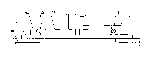
本実施例では、温調板32とアンテナ収納部材20は別個の部材であったが、温調板32の機能をアンテナ収納部材20にもたせてもよい。例えば、アンテナ収納部材20の上面及び/又は側面に流路33を形成することによりアンテナ収納部材20を直接冷却することができる。また、図5に示すように、アンテナ収納部材20の側面に流路33に類似の流路99を有する温調板98を形成すれば、波長短縮部材22とスロット電極24とを同時に冷却することも可能である。ここで、図5は、図1に示すマイクロ波プラズマ装置100の温調板32の変形例を示す部分拡大断面図である。また、スロット電極24の周囲に温調板を設けたり、若しくは、スリット25の配置を妨げないようにスロット電極24自体に流路を形成することもできる。
【0037】
誘電体28はスロット電極24と処理室40との間に配置されている。スロット電極24と誘電体28は、例えば、ロウにより強固にかつ機密に面接合される。代替的に、焼成されたセラミック製の誘電体28の裏面に、スクリーン印刷などの手段により銅薄膜を、スリットを含むスロット電極24の形状にパターン形成して、これを焼き付けるように銅箔のスロット電極24を形成してもよい。誘電体28と処理室40はオーリング90によって接合されている。誘電体28の周辺を例えば80℃乃至100℃に温調する第3の温度制御装置95が設けられる場合には、図4に示すように構成される。第3の温度制御装置95は温調板32と同様に誘電体28を取り囲む流路96を有している。このように第3の温度制御装置は、オーリング90の近傍に設けられているため、誘電体28及びスロット電極24を温調すると共にオーリング90の温調も効果的に行うことができる。誘電体28は、窒化アルミニウム(AlN)などからなり、減圧又は真空環境にある処理室40の圧力がスロット電極24に印加されてスロット電極24が変形したり、スロット電極24が処理室40に剥き出しになってスパッタされたり銅汚染を発生したりすることを防止している。必要があれば、誘電体28を熱伝導率の低い材質で構成することによって、スロット電極24が処理室40の温度により影響を受けるのを防止してもよい。
【0038】
選択的に、誘電体28は、波長短縮部材22と同様に、熱伝導率の高い材質(例えば、AlN)で形成することができる。この場合は、誘電体28の温度を制御することによってスロット電極24の温度制御を行うことができ、スロット電極24を介して波長短縮部材22の温度制御を行うことができる。この場合、誘電体28の内部にマイクロ波の処理室40への導入を妨げないように流路を形成することも可能である。なお、上述した温度制御は任意に組み合わせることもできる。
【0039】
処理室40は、側壁や底部がアルミニウムなどの導体により構成されて、全体が筒状に成形されており、内部は後述する真空ポンプ60により所定の減圧又は真空密閉空間に維持されることができる。処理室40内には、熱板42とその上に被処理体である半導体ウェハWが収納されている。なお、図1においては、半導体ウェハWを固定する静電チャックやクランプ機構などは便宜上省略されている。
【0040】
熱板42は、ヒータ装置38と同様の構成を有して、半導体ウェハWの温度制御を行う。例えば、プラズマCVD処理においては、熱板42は、半導体ウェハWを例示的に約450℃に加熱する。また、プラズマエッチング処理においては、熱板42は、半導体ウェハWを例示的に約80℃以下に加熱する。熱板42によるこれらの加熱温度はプロセスにより異なる。いずれにしろ、熱板42は、半導体ウェハWに不純物としての水分が付着・混入しないように半導体ウェハWを加熱する。第2の温度制御装置70は、熱板42の温度を測定する温度センサ72が測定した温度に従って熱板42に流れる加熱用電流の大きさを制御することができる。
【0041】
処理室40の側壁には、反応ガスを導入するための石英パイプ製ガス供給ノズル50が設けられ、このノズル50は、ガス供給路52によりマスフローコントローラ54及び開閉弁56を介して反応ガス源58に接続されている。例えば、窒化シリコン膜を堆積させようとする場合には、反応ガスとして所定の混合ガス(即ち、ネオン,キセノン、アルゴン、ヘリウム、ラドン、クリプトンのいずれかにN2とH2を加えたもの)にNH3やSiH4ガスなどを混合したものが選択されることができる。
【0042】
真空ポンプ60は、処理室40の圧力を所定の圧力(例えば、0.1乃至数10mTorr)まで真空引きすることができる。なお、図1においては、排気系の詳細な構造も省略されている。
【0043】
次に、以上のように構成された本実施例のマイクロ波プラズマ処理装置100の動作について説明する。まず、通常処理室40の側壁に設けられている図示しないゲートバルブを介して半導体ウェハWを搬送アームにより処理室40に収納する。その後、図示しないリフタピンを上下動させることによって半導体ウェハWを所定の載置面に配置する。
【0044】
次に、処理室40内を所定の処理圧力、例えば、50mTorrに維持してノズル50から、例えば、ヘリウム、窒素及び水素の混合ガスにNH3を更に混合した一以上の反応ガス源58からマスフローコントローラ54及び開閉弁56を介して流量制御しつつ処理室40に導入される。
【0045】
処理室40の温度は70℃程度になるように第2の温度制御装置70と熱板42により調整される。また、第1の温度制御装置30は、温調板32の温度が70℃程度になるようにヒータ装置38を制御する。これにより、温調板32を介して波長短縮部材22とスロット電極24の温度も70℃程度に維持される。スロット電極24は70℃で最適のスリット長を有するように設計されている。また、スロット電極24は±5℃程度の温度誤差が許容範囲であるということが予め分かっているものとする。プラズマが発生する際には、スロット電極がプラズマによる熱で加熱されるのでスロットも所定の温度以下になった時にマイクロ波を供給するようにしてプラズマ立上げ時の熱を抑制するように制御してもよい。
【0046】
一方、マイクロ波源10からのマイクロ波を図示しない矩形導波管や同軸導波管などを介してアンテナ収納部材20内の波長短縮部材22に、例えば、TEMモードなどで導入する。波長短縮部材22を通過したマイクロ波はその波長が短縮されてスロット電極24に入射し、スリット25から処理室40に誘電体28を介して導入される。波長短縮部材22とスロット電極24は温度制御されているので、熱膨張などによる変形はなく、スロット電極24は最適なスリット長さを維持することができる。これによってマイクロ波は、均一に(即ち、部分的集中なしに)かつ全体として所望の密度で(即ち、密度の低下なしに)処理室40に導入されることができる。
【0047】
継続的な使用により、温調板32の温度が75℃よりも上昇すれば第1の温度制御装置30は水源39より15℃程度の冷却水を温調板32に導入することによりこれを75℃以内になるように制御する。同様に、処理開始時や過冷却により温調板32の温度が65℃以下になれば第1の温度制御装置30はヒータ装置38を制御して水源39から温調板32に導入される水温を上げて温調板32の温度を65℃以上にすることができる。
【0048】
一方、温調板32による過冷却によって処理室40の温度が所定温度以下になったことを温度センサ72が検知すれば、水分が不純物としてウェハWに付着・混入することを防ぐため第2の温度制御装置70は熱板42を制御して処理室40の温度を制御することができる。
【0049】
その後、マイクロ波は、反応ガスをプラズマ化して成膜処理を行う。成膜処理は、例えば、予め設定された所定時間だけ行われてその後、半導体ウェハWは上述の図示しないゲートバルブから処理室40の外へ出される。処理室40には所望の密度のマイクロ波が均一に供給されるのでウェハWには所望の厚さの膜が均一に形成されることになる。また、処理室40の温度は水分などがウェハWに混入することのない温度に維持されるので所望の成膜品質を維持することができる。
【0050】
以上、本発明の好ましい実施例を説明したが、本発明はその要旨の範囲内で種々の変形及び変更が可能である。例えば、本発明のマイクロ波プラズマ処理装置100は電子サイクロトロン共鳴の利用を妨げるものではないため、所定の磁場を発生させるコイルなどを有してもよい。また、本実施例のマイクロ波プラズマ処理装置100はプラズマCVD装置として説明されているが、マイクロ波プラズマ処理装置100は半導体ウェハWをエッチングしたりクリーニングしたりする場合にも使用することができることはいうまでもない。更に、本発明で処理される被処理体は半導体ウェハに限られず、LCDなどを含むものである。
【0051】
【発明の効果】
本発明のマイクロ波プラズマ装置によれば一以上の温度制御により均一な処理を達成することができる。
【図面の簡単な説明】
【図1】 本実施例の例示的なマイクロ波プラズマ処理装置の構造を示す概略ブロック図である。
【図2】 図1に示すマイクロ波プラズマ処理装置に使用されるスロット電極の具体的構成例を説明するための概略平面図である。
【図3】 図1に示すマイクロ波プラズマ処理装置に使用される第1の温度制御装置と温調板の構成を示す概略ブロック図である。
【図4】 第3の温度制御装置95を説明するための部分拡大断面図である。
【図5】 図1に示すマイクロ波プラズマ装置の温調板の変形例を示す部分拡大断面図である。
【符号の説明】
10 マイクロ波源
20 アンテナ収納部材
22 波長短縮部材
24 スロット電極
25 スリット
28 誘電体
30 第1の温度制御装置
32 温調板
36 温度センサ
38 ヒータ装置
39 水源
40 処理室
42 熱板
50 反応ガス供給ノズル
58 反応ガス源
60 真空ポンプ
70 第2の温度制御装置
72 温度センサ[0001]
[0002]
BACKGROUND OF THE INVENTION
The present invention relates to a microwave plasma processing apparatus and method.
[0003]
[Prior art]
In recent years, with the increase in density and miniaturization of semiconductor products, plasma processing apparatuses are sometimes used for processes such as film formation, etching, and ashing in the manufacturing process of semiconductor products. In particular, a microwave plasma apparatus that generates high-density plasma by combining a microwave and a magnetic field from a ring coil has been proposed because it can stably generate a plasma even under a reduced pressure of about 0.1 to 10 mTorr.
[0004]
In a typical microwave plasma apparatus, for example, a microwave of about 2.45 GHz passes through a waveguide, a transmission window, and a slot electrode in this order, and the processing object is placed and maintained in a reduced pressure environment. To be introduced. On the other hand, a reactive gas is also introduced into the processing chamber, and is converted into plasma by microwaves to form radicals and ions with strong activity, which react with the object to be processed and perform etching.
[0005]
The microwave may be passed through a dielectric (hereinafter referred to as “wavelength shortening member”) that shortens the wavelength of the microwave before being introduced into the slot electrode. Thereby, since the wavelength of the microwave is shortened, the interval between the slits formed in the slot electrode can be shortened. The wavelength shortening member is disclosed in, for example, Japanese Patent Laid-Open No. 9-63793, which has already been filed by the present applicant.
[0006]
The transmission window is made of quartz, alumina, or the like, but is damaged or weakened by being heated by plasma heat. The wavelength shortening member and the slot electrode are also thermally expanded by the plasma heat. For example, although the slot electrode is formed of a copper plate or the like, the optimum slit length changes due to thermal expansion, and the overall plasma density in the processing chamber is lowered or the plasma density is partially concentrated. If the overall plasma density decreases, the processing speed of the semiconductor wafer changes. As a result, when the plasma processing is managed in terms of time, the desired processing (etching depth or film thickness) is not formed on the semiconductor wafer even if the processing is stopped for a predetermined time (for example, 2 minutes). There is a case. Further, if the plasma density is partially concentrated, the processing of the semiconductor wafer is partially changed.
[0007]
In order to solve this problem, for example, Japanese Patent Laid-Open No. 3-191073 proposes a microwave plasma processing apparatus that provides cooling means using cooling water to cool the transmission window. Japanese Patent Laid-Open No. 9-63793 mentioned above proposes to provide a cooling jacket on the wavelength shortening member and the slot electrode covering member (see paragraph [0008]).
[0009]
[Problems to be solved by the invention]
However, in the plasma CVD apparatus, if moisture remains in the form of liquid or mist, it enters the film formed on the semiconductor wafer as impurities, so that the temperature of the processing chamber is preferably raised as much as possible. However, simply providing a cooling means as disclosed in Japanese Patent Laid-Open No. 3-191073 degrades the quality of plasma processing. Thus, conventionally, it has not been possible to remove the harmful effects of plasma heat while maintaining the quality of the object to be processed.
[0010]
In addition, it is necessary to control a member having low resistance to high temperatures such as an O-ring that joins the processing chamber and the dielectric so that a temperature higher than a certain temperature is not applied. As another problem, Japanese Patent Application Laid-Open No. 9-63793 does not disclose what kind of material is used for the wavelength shortening member, and heat conduction becomes difficult unless the material is taken into consideration. For this reason, it becomes difficult to control the temperature, and the uniformity of processing is deteriorated.
[0011]
Accordingly, it is a general object of the present invention to provide a microwave plasma processing apparatus and method that can operate in a new and useful reduced pressure environment that solves such problems.
[0012]
[Means for Solving the Problems]
The microwave processing apparatus according to an exemplary embodiment of the present invention is connected to the wavelength shortening member that shortens the wavelength of the microwave when the microwave is introduced, and passes through the wavelength shortening member. A slot electrode that guides the microwave, a first temperature control device that can control the temperature of the wavelength shortening member and the slot electrode, a reactive gas source that supplies a reactive gas, and a vacuum pump that can be connected. A processing chamber that can store a processing object and that can perform a predetermined process on the target object under a reduced pressure environment when the microwave and the reaction gas that have passed through the slot electrode are supplied. . The first temperature control device may control the slot electrode to a temperature that suppresses moisture from adhering to the processing chamber. The first temperature control device may control the temperature of the slot electrode to 70 ° C. ± 10 ° C. In addition, the first temperature control device can control the temperature of one of the wavelength shortening member and the slot electrode, and can also control the other temperature using the thermal conductivity of the one.
[0013]
The microwave plasma processing apparatus further includes an antenna housing member that houses the wavelength shortening member and is connected to the slot electrode, and the first temperature control device controls a temperature of the antenna housing member. Thus, the temperature of the wavelength shortening member and the slot electrode can be controlled using the thermal conductivity of the antenna housing member. The microwave plasma processing apparatus further includes a dielectric disposed between the slot electrode and the processing chamber, and the first temperature controller includes the wavelength shortening member, the slot electrode, and the dielectric. The temperature of the slot electrode can be controlled by controlling one temperature and utilizing the one thermal conductivity. Further, the microwave plasma device may be a second temperature control device that controls the temperature of the object to be processed to be a predetermined processing temperature or a third temperature control that controls the temperature of the periphery of the plasma device. A device can further be included.
[0014]
A plasma processing method according to an exemplary embodiment of the present invention includes a step of storing an object to be processed in a processing chamber, a step of controlling the pressure in the processing chamber, a step of controlling the temperature of the slot electrode, and a reactive gas. Introducing the processing chamber, supplying a microwave to the slot electrode, and processing the object to be processed with the plasma by the microwave. The temperature control step includes the step of controlling the temperature of a wavelength shortening member operable to shorten the wavelength of the microwave, and the thermal control from the temperature controlled wavelength shortening member to the slot electrode only. And a step of controlling the temperature of the slot electrode.
[0015]
The plasma processing method according to another exemplary embodiment of the present invention includes a step of storing an object to be processed in a processing chamber, a step of controlling the pressure in the processing chamber, a step of controlling the temperature of the slot electrode, and a reactive gas. A step of introducing a microwave into the processing chamber, a step of supplying a microwave to the slot electrode when the slot electrode is below a predetermined temperature, and a step of processing the object to be processed with the plasma by the microwave. Have. The temperature control step includes a step of controlling the temperature of a wavelength shortening member operable to shorten the wavelength of the microwave to a predetermined temperature or less, and only heat conduction from the temperature controlled wavelength shortening member to the slot electrode. And the step of controlling the temperature of the slot electrode using
[0016]
In any of the above-described plasma processing methods, the temperature control step includes only the step of controlling the temperature of the dielectric connected to the slot electrode, and the heat conduction from the temperature-controlled dielectric to the slot electrode. And may further comprise a step of controlling the temperature of the object to be processed.
[0017]
DETAILED DESCRIPTION OF THE INVENTION
Hereinafter, an exemplary
[0018]
The
[0019]
A
[0020]
For the
[0021]
The
[0022]
[Expression 1]
[0023]
A first
[0024]
As the
[0025]
The
[0026]
The
[0027]
If the
[0028]
For example, in the
[0029]
Further, if the
[0030]
On the other hand, the
[0031]
In this case, the first
[0032]
Since the temperature of the
[0033]
As described above, the first
[0034]
In addition, the first
[0035]
Next, the
[0036]
In this embodiment, the
[0037]
The dielectric 28 is disposed between the
[0038]
Alternatively, the dielectric 28 can be formed of a material having high thermal conductivity (for example, AlN), similar to the
[0039]
The
[0040]
The
[0041]
A
[0042]
The
[0043]
Next, the operation of the microwave
[0044]
Next, the inside of the
[0045]
The temperature of the
[0046]
On the other hand, the microwave from the
[0047]
If the temperature of the
[0048]
On the other hand, if the
[0049]
After that, the microwave performs the film forming process by converting the reaction gas into plasma. The film forming process is performed, for example, for a predetermined time set in advance, and then the semiconductor wafer W is taken out of the
[0050]
Although the preferred embodiments of the present invention have been described above, the present invention can be variously modified and changed within the scope of the gist thereof. For example, since the microwave
[0051]
【The invention's effect】
According to the microwave plasma apparatus of the present invention, uniform processing can be achieved by controlling one or more temperatures.
[Brief description of the drawings]
FIG. 1 is a schematic block diagram showing the structure of an exemplary microwave plasma processing apparatus of the present embodiment.
FIG. 2 is a schematic plan view for explaining a specific configuration example of a slot electrode used in the microwave plasma processing apparatus shown in FIG.
FIG. 3 is a schematic block diagram showing the configuration of a first temperature control device and a temperature control plate used in the microwave plasma processing apparatus shown in FIG. 1;
4 is a partially enlarged cross-sectional view for explaining a third
FIG. 5 is a partially enlarged cross-sectional view showing a modification of the temperature control plate of the microwave plasma apparatus shown in FIG.
[Explanation of symbols]
10 Microwave source
20 Antenna housing member
22 Wavelength shortening member
24 slot electrode
25 slits
28 Dielectric
30 First temperature control device
32 Temperature control board
36 Temperature sensor
38 Heater device
39 Water source
40 treatment room
42 Hot plate
50 Reaction gas supply nozzle
58 Reaction gas source
60 Vacuum pump
70 Second temperature control device
72 Temperature sensor
Claims (9)
当該波長短縮部材に接続され、前記波長短縮部材を通過した前記マイクロ波を案内するスロット電極と、
前記波長短縮部材の加熱及び冷却を制御するか、又は、前記スロット電極に接続される他の部材の加熱及び冷却を制御することによって前記波長短縮部材及び前記スロット電極の温度を制御する第1の温度制御装置と、
反応ガスを供給する反応ガス源及び真空ポンプに接続可能で被処理体を収納し、前記スロット電極を通過した前記マイクロ波と前記反応ガスが供給されると、減圧環境下で前記被処理体にマイクロ波プラズマ処理を施す処理室とを有するマイクロ波プラズマ処理装置。A wavelength shortening member that shortens the wavelength of the microwave when the microwave is introduced;
A slot electrode that is connected to the wavelength shortening member and guides the microwave that has passed through the wavelength shortening member;
Controlling the heating and cooling of the wavelength shortening member, or controlling the temperature of the wavelength shortening member and the slot electrode by controlling the heating and cooling of other members connected to the slot electrode. A temperature control device;
It can be connected to a reaction gas source for supplying a reaction gas and a vacuum pump, accommodates an object to be processed, and when the microwave and the reaction gas that have passed through the slot electrode are supplied, A microwave plasma processing apparatus having a processing chamber for performing microwave plasma processing.
前記処理室内の圧力を制御する工程と、
スロット電極の温度と当該スロット電極に接続されてマイクロ波の波長を短縮するように動作可能な波長短縮部材の温度を、前記波長短縮部材の加熱及び冷却を制御するか、又は、前記スロット電極に接続される他の部材の加熱及び冷却を制御することによって制御する工程と、
反応ガスを前記処理室内に導入する工程と、
マイクロ波を前記スロット電極に供給する工程と、
前記マイクロ波によるプラズマで前記被処理体を処理する工程とを有するプラズマ処理方法。Storing the object to be processed in the processing chamber;
Controlling the pressure in the processing chamber;
The temperature of the wavelength shortening member connected to the slot electrode and operable to shorten the wavelength of the microwave is controlled to control the heating and cooling of the wavelength shortening member, or to the slot electrode. Controlling by controlling heating and cooling of other members to be connected;
Introducing a reaction gas into the processing chamber;
Supplying a microwave to the slot electrode;
And a step of processing the object to be processed with the plasma by the microwave.
Priority Applications (2)
| Application Number | Priority Date | Filing Date | Title |
|---|---|---|---|
| JP08567599A JP4053173B2 (en) | 1999-03-29 | 1999-03-29 | Microwave plasma processing apparatus and method |
| US09/536,721 US6736930B1 (en) | 1999-03-29 | 2000-03-28 | Microwave plasma processing apparatus for controlling a temperature of a wavelength reducing member |
Applications Claiming Priority (1)
| Application Number | Priority Date | Filing Date | Title |
|---|---|---|---|
| JP08567599A JP4053173B2 (en) | 1999-03-29 | 1999-03-29 | Microwave plasma processing apparatus and method |
Publications (2)
| Publication Number | Publication Date |
|---|---|
| JP2000277508A JP2000277508A (en) | 2000-10-06 |
| JP4053173B2 true JP4053173B2 (en) | 2008-02-27 |
Family
ID=13865419
Family Applications (1)
| Application Number | Title | Priority Date | Filing Date |
|---|---|---|---|
| JP08567599A Expired - Fee Related JP4053173B2 (en) | 1999-03-29 | 1999-03-29 | Microwave plasma processing apparatus and method |
Country Status (2)
| Country | Link |
|---|---|
| US (1) | US6736930B1 (en) |
| JP (1) | JP4053173B2 (en) |
Cited By (1)
| Publication number | Priority date | Publication date | Assignee | Title |
|---|---|---|---|---|
| KR101332252B1 (en) * | 2011-02-23 | 2013-11-22 | 도쿄엘렉트론가부시키가이샤 | Microwave irradiation apparatus |
Families Citing this family (16)
| Publication number | Priority date | Publication date | Assignee | Title |
|---|---|---|---|---|
| JP2000299199A (en) * | 1999-04-13 | 2000-10-24 | Plasma System Corp | Plasma generator and plasma processing apparatus |
| JP4402860B2 (en) * | 2001-03-28 | 2010-01-20 | 忠弘 大見 | Plasma processing equipment |
| JP5010781B2 (en) * | 2001-03-28 | 2012-08-29 | 忠弘 大見 | Plasma processing equipment |
| JP4183934B2 (en) * | 2001-10-19 | 2008-11-19 | 尚久 後藤 | Microwave plasma processing apparatus, microwave plasma processing method, and microwave power supply apparatus |
| JP4136630B2 (en) * | 2002-12-03 | 2008-08-20 | キヤノン株式会社 | Plasma processing equipment |
| US20070137575A1 (en) * | 2003-11-05 | 2007-06-21 | Tokyo Electron Limited | Plasma processing apparatus |
| JP4361811B2 (en) * | 2004-01-09 | 2009-11-11 | 東京エレクトロン株式会社 | Semiconductor manufacturing equipment |
| JP2005310478A (en) * | 2004-04-20 | 2005-11-04 | Naohisa Goto | Plasma processing apparatus and processing method, and flat panel display manufacturing method |
| JP4149427B2 (en) * | 2004-10-07 | 2008-09-10 | 東京エレクトロン株式会社 | Microwave plasma processing equipment |
| US8454749B2 (en) * | 2005-12-19 | 2013-06-04 | Tokyo Electron Limited | Method and system for sealing a first assembly to a second assembly of a processing system |
| WO2013176144A1 (en) * | 2012-05-25 | 2013-11-28 | 東京エレクトロン株式会社 | Plasma processing device and plasma processing method |
| FR3012030B1 (en) | 2013-10-18 | 2015-12-25 | Medicrea International | METHOD FOR REALIZING THE IDEAL CURVATURE OF A ROD OF A VERTEBRAL OSTEOSYNTHESIS EQUIPMENT FOR STRENGTHENING THE VERTEBRAL COLUMN OF A PATIENT |
| US10039157B2 (en) | 2014-06-02 | 2018-07-31 | Applied Materials, Inc. | Workpiece processing chamber having a rotary microwave plasma source |
| US10269541B2 (en) * | 2014-06-02 | 2019-04-23 | Applied Materials, Inc. | Workpiece processing chamber having a thermal controlled microwave window |
| US11244808B2 (en) | 2017-05-26 | 2022-02-08 | Applied Materials, Inc. | Monopole antenna array source for semiconductor process equipment |
| KR102417936B1 (en) | 2017-08-04 | 2022-07-07 | 주식회사 다이셀 | Anti-glare film |
Family Cites Families (16)
| Publication number | Priority date | Publication date | Assignee | Title |
|---|---|---|---|---|
| JPS6436085A (en) * | 1987-07-31 | 1989-02-07 | Canon Kk | Method and apparatus for forming functional deposition film by microwave plasma cvd method |
| JPS6472526A (en) * | 1987-09-14 | 1989-03-17 | Hitachi Ltd | Microwave plasma processor |
| JPH02197575A (en) * | 1989-01-26 | 1990-08-06 | Canon Inc | Microwave plasma cvd method and device therefor |
| US5134965A (en) * | 1989-06-16 | 1992-08-04 | Hitachi, Ltd. | Processing apparatus and method for plasma processing |
| JPH03191073A (en) | 1989-12-21 | 1991-08-21 | Canon Inc | Microwave plasma treating device |
| JP3191073B2 (en) | 1993-09-08 | 2001-07-23 | 株式会社アドバンテスト | Polycrystalline silicon thin film transistor array inspection system |
| JP3136054B2 (en) | 1994-08-16 | 2001-02-19 | 東京エレクトロン株式会社 | Plasma processing equipment |
| JPH0963793A (en) | 1995-08-25 | 1997-03-07 | Tokyo Electron Ltd | Plasma processing device |
| US5698036A (en) * | 1995-05-26 | 1997-12-16 | Tokyo Electron Limited | Plasma processing apparatus |
| JP4068175B2 (en) * | 1996-06-12 | 2008-03-26 | 株式会社東芝 | Plasma processing equipment |
| JP2921499B2 (en) * | 1996-07-30 | 1999-07-19 | 日本電気株式会社 | Plasma processing equipment |
| US5935334A (en) * | 1996-11-13 | 1999-08-10 | Applied Materials, Inc. | Substrate processing apparatus with bottom-mounted remote plasma system |
| US5824607A (en) * | 1997-02-06 | 1998-10-20 | Applied Materials, Inc. | Plasma confinement for an inductively coupled plasma reactor |
| US5937323A (en) * | 1997-06-03 | 1999-08-10 | Applied Materials, Inc. | Sequencing of the recipe steps for the optimal low-k HDP-CVD processing |
| JP3662101B2 (en) * | 1997-10-27 | 2005-06-22 | 東京エレクトロン株式会社 | Plasma processing equipment |
| JPH11339997A (en) * | 1998-05-30 | 1999-12-10 | Tokyo Electron Ltd | Plasma processing equipment |
-
1999
- 1999-03-29 JP JP08567599A patent/JP4053173B2/en not_active Expired - Fee Related
-
2000
- 2000-03-28 US US09/536,721 patent/US6736930B1/en not_active Expired - Fee Related
Cited By (2)
| Publication number | Priority date | Publication date | Assignee | Title |
|---|---|---|---|---|
| KR101332252B1 (en) * | 2011-02-23 | 2013-11-22 | 도쿄엘렉트론가부시키가이샤 | Microwave irradiation apparatus |
| US9224623B2 (en) | 2011-02-23 | 2015-12-29 | Tokyo Electron Limited | Microwave irradiation apparatus |
Also Published As
| Publication number | Publication date |
|---|---|
| US6736930B1 (en) | 2004-05-18 |
| JP2000277508A (en) | 2000-10-06 |
Similar Documents
| Publication | Publication Date | Title |
|---|---|---|
| JP4053173B2 (en) | Microwave plasma processing apparatus and method | |
| JP4849705B2 (en) | Plasma processing apparatus, plasma generation introducing member, and dielectric | |
| KR101243632B1 (en) | Substrate processing apparatus and method of manufacturing semiconductor device | |
| JP4889683B2 (en) | Deposition equipment | |
| US20110217849A1 (en) | Device and method for producing dielectric layers in microwave plasma | |
| JP2001274151A (en) | Plasma processing apparatus and method, gas supply ring and dielectric | |
| JP2008522446A (en) | Method and apparatus for controlling spatial temperature distribution | |
| KR20100138580A (en) | Plasma dry etching apparatus having cold coupling means for raising and lowering the outermost temperature of the wafer depending on the material film to be etched and the gas to be used. | |
| JP5121684B2 (en) | Plasma processing equipment | |
| CN110867363A (en) | Plasma processing apparatus | |
| TW201218300A (en) | Substrate processing apparatus and method of manufacturing a semiconductor device | |
| CN101218860A (en) | Plasma processing apparatus | |
| JP4583618B2 (en) | Plasma processing equipment | |
| CN112420510A (en) | Heat treatment method and heat treatment device | |
| JP4742431B2 (en) | Heat treatment equipment | |
| JP3986204B2 (en) | Plasma processing apparatus and method | |
| US12262460B2 (en) | Fast annealing equipment | |
| JP4226135B2 (en) | Microwave plasma processing apparatus and method | |
| JP4580235B2 (en) | Formation method of insulating film | |
| JP4255163B2 (en) | Microwave plasma equipment | |
| JP2006054206A (en) | Plasma processing apparatus and method | |
| US7569497B2 (en) | Method and apparatus for forming insulating layer | |
| JP2923879B2 (en) | Plasma processing equipment | |
| JPH06252093A (en) | Pressure control method and its device | |
| JP2008106366A (en) | Film-forming apparatus |
Legal Events
| Date | Code | Title | Description |
|---|---|---|---|
| A621 | Written request for application examination |
Free format text: JAPANESE INTERMEDIATE CODE: A621 Effective date: 20050427 |
|
| A977 | Report on retrieval |
Free format text: JAPANESE INTERMEDIATE CODE: A971007 Effective date: 20060413 |
|
| A131 | Notification of reasons for refusal |
Free format text: JAPANESE INTERMEDIATE CODE: A131 Effective date: 20060418 |
|
| A521 | Request for written amendment filed |
Free format text: JAPANESE INTERMEDIATE CODE: A523 Effective date: 20060616 |
|
| A131 | Notification of reasons for refusal |
Free format text: JAPANESE INTERMEDIATE CODE: A131 Effective date: 20070703 |
|
| A521 | Request for written amendment filed |
Free format text: JAPANESE INTERMEDIATE CODE: A523 Effective date: 20070830 |
|
| A131 | Notification of reasons for refusal |
Free format text: JAPANESE INTERMEDIATE CODE: A131 Effective date: 20070925 |
|
| A521 | Request for written amendment filed |
Free format text: JAPANESE INTERMEDIATE CODE: A523 Effective date: 20071107 |
|
| TRDD | Decision of grant or rejection written | ||
| A01 | Written decision to grant a patent or to grant a registration (utility model) |
Free format text: JAPANESE INTERMEDIATE CODE: A01 Effective date: 20071204 |
|
| A61 | First payment of annual fees (during grant procedure) |
Free format text: JAPANESE INTERMEDIATE CODE: A61 Effective date: 20071205 |
|
| FPAY | Renewal fee payment (event date is renewal date of database) |
Free format text: PAYMENT UNTIL: 20101214 Year of fee payment: 3 |
|
| R150 | Certificate of patent or registration of utility model |
Free format text: JAPANESE INTERMEDIATE CODE: R150 |
|
| FPAY | Renewal fee payment (event date is renewal date of database) |
Free format text: PAYMENT UNTIL: 20101214 Year of fee payment: 3 |
|
| FPAY | Renewal fee payment (event date is renewal date of database) |
Free format text: PAYMENT UNTIL: 20131214 Year of fee payment: 6 |
|
| R250 | Receipt of annual fees |
Free format text: JAPANESE INTERMEDIATE CODE: R250 |
|
| LAPS | Cancellation because of no payment of annual fees |