JP4046118B2 - LIGHT EMITTING ELEMENT, LIGHT EMITTING DEVICE USING SAME, AND SURFACE EMITTING LIGHTING DEVICE - Google Patents
LIGHT EMITTING ELEMENT, LIGHT EMITTING DEVICE USING SAME, AND SURFACE EMITTING LIGHTING DEVICE Download PDFInfo
- Publication number
- JP4046118B2 JP4046118B2 JP2004508420A JP2004508420A JP4046118B2 JP 4046118 B2 JP4046118 B2 JP 4046118B2 JP 2004508420 A JP2004508420 A JP 2004508420A JP 2004508420 A JP2004508420 A JP 2004508420A JP 4046118 B2 JP4046118 B2 JP 4046118B2
- Authority
- JP
- Japan
- Prior art keywords
- light
- light emitting
- emitting element
- translucent
- diode structure
- Prior art date
- Legal status (The legal status is an assumption and is not a legal conclusion. Google has not performed a legal analysis and makes no representation as to the accuracy of the status listed.)
- Expired - Fee Related
Links
- 239000000758 substrate Substances 0.000 claims description 221
- 239000000463 material Substances 0.000 claims description 64
- 229920005989 resin Polymers 0.000 claims description 60
- 239000011347 resin Substances 0.000 claims description 60
- 239000004065 semiconductor Substances 0.000 claims description 56
- 230000003287 optical effect Effects 0.000 claims description 34
- 238000005286 illumination Methods 0.000 claims description 29
- OAICVXFJPJFONN-UHFFFAOYSA-N Phosphorus Chemical compound [P] OAICVXFJPJFONN-UHFFFAOYSA-N 0.000 claims description 14
- 230000002093 peripheral effect Effects 0.000 claims description 7
- 230000005284 excitation Effects 0.000 claims description 5
- 238000010030 laminating Methods 0.000 claims description 5
- 230000037237 body shape Effects 0.000 claims 1
- 239000010410 layer Substances 0.000 description 93
- 238000000605 extraction Methods 0.000 description 67
- 238000009826 distribution Methods 0.000 description 37
- 238000012986 modification Methods 0.000 description 29
- 230000004048 modification Effects 0.000 description 29
- 229910052594 sapphire Inorganic materials 0.000 description 20
- 239000010980 sapphire Substances 0.000 description 20
- 230000004907 flux Effects 0.000 description 19
- 238000000034 method Methods 0.000 description 14
- 239000003822 epoxy resin Substances 0.000 description 11
- 229920000647 polyepoxide Polymers 0.000 description 11
- 229920002050 silicone resin Polymers 0.000 description 10
- 238000004088 simulation Methods 0.000 description 9
- 239000004925 Acrylic resin Substances 0.000 description 8
- 229920000178 Acrylic resin Polymers 0.000 description 8
- 238000012545 processing Methods 0.000 description 7
- NCGICGYLBXGBGN-UHFFFAOYSA-N 3-morpholin-4-yl-1-oxa-3-azonia-2-azanidacyclopent-3-en-5-imine;hydrochloride Chemical compound Cl.[N-]1OC(=N)C=[N+]1N1CCOCC1 NCGICGYLBXGBGN-UHFFFAOYSA-N 0.000 description 6
- 238000010586 diagram Methods 0.000 description 6
- 230000000694 effects Effects 0.000 description 6
- 230000017525 heat dissipation Effects 0.000 description 5
- 230000007423 decrease Effects 0.000 description 4
- 238000004519 manufacturing process Methods 0.000 description 4
- 238000007789 sealing Methods 0.000 description 4
- 239000000126 substance Substances 0.000 description 4
- NIXOWILDQLNWCW-UHFFFAOYSA-N acrylic acid group Chemical group C(C=C)(=O)O NIXOWILDQLNWCW-UHFFFAOYSA-N 0.000 description 3
- 239000000853 adhesive Substances 0.000 description 3
- 230000001070 adhesive effect Effects 0.000 description 3
- 238000006243 chemical reaction Methods 0.000 description 3
- 230000006866 deterioration Effects 0.000 description 3
- 239000011521 glass Substances 0.000 description 3
- 238000013041 optical simulation Methods 0.000 description 3
- 229910052782 aluminium Inorganic materials 0.000 description 2
- 238000009434 installation Methods 0.000 description 2
- XAGFODPZIPBFFR-UHFFFAOYSA-N aluminium Chemical compound [Al] XAGFODPZIPBFFR-UHFFFAOYSA-N 0.000 description 1
- 238000013459 approach Methods 0.000 description 1
- 229910052681 coesite Inorganic materials 0.000 description 1
- 238000011109 contamination Methods 0.000 description 1
- 229910052906 cristobalite Inorganic materials 0.000 description 1
- 238000009792 diffusion process Methods 0.000 description 1
- WABPQHHGFIMREM-UHFFFAOYSA-N lead(0) Chemical compound [Pb] WABPQHHGFIMREM-UHFFFAOYSA-N 0.000 description 1
- 229910001635 magnesium fluoride Inorganic materials 0.000 description 1
- 238000012423 maintenance Methods 0.000 description 1
- 229910052751 metal Inorganic materials 0.000 description 1
- 239000002184 metal Substances 0.000 description 1
- 238000000465 moulding Methods 0.000 description 1
- 229920003217 poly(methylsilsesquioxane) Polymers 0.000 description 1
- 238000007650 screen-printing Methods 0.000 description 1
- 238000004904 shortening Methods 0.000 description 1
- 239000000377 silicon dioxide Substances 0.000 description 1
- VYPSYNLAJGMNEJ-UHFFFAOYSA-N silicon dioxide Inorganic materials O=[Si]=O VYPSYNLAJGMNEJ-UHFFFAOYSA-N 0.000 description 1
- 229910052709 silver Inorganic materials 0.000 description 1
- 239000002356 single layer Substances 0.000 description 1
- 229910052682 stishovite Inorganic materials 0.000 description 1
- 229910052905 tridymite Inorganic materials 0.000 description 1
- 238000007740 vapor deposition Methods 0.000 description 1
Images


Classifications
-
- H—ELECTRICITY
- H10—SEMICONDUCTOR DEVICES; ELECTRIC SOLID-STATE DEVICES NOT OTHERWISE PROVIDED FOR
- H10H—INORGANIC LIGHT-EMITTING SEMICONDUCTOR DEVICES HAVING POTENTIAL BARRIERS
- H10H20/00—Individual inorganic light-emitting semiconductor devices having potential barriers, e.g. light-emitting diodes [LED]
- H10H20/80—Constructional details
- H10H20/81—Bodies
- H10H20/819—Bodies characterised by their shape, e.g. curved or truncated substrates
-
- G—PHYSICS
- G02—OPTICS
- G02B—OPTICAL ELEMENTS, SYSTEMS OR APPARATUS
- G02B5/00—Optical elements other than lenses
- G02B5/02—Diffusing elements; Afocal elements
- G02B5/0205—Diffusing elements; Afocal elements characterised by the diffusing properties
- G02B5/021—Diffusing elements; Afocal elements characterised by the diffusing properties the diffusion taking place at the element's surface, e.g. by means of surface roughening or microprismatic structures
- G02B5/0231—Diffusing elements; Afocal elements characterised by the diffusing properties the diffusion taking place at the element's surface, e.g. by means of surface roughening or microprismatic structures the surface having microprismatic or micropyramidal shape
-
- G—PHYSICS
- G02—OPTICS
- G02B—OPTICAL ELEMENTS, SYSTEMS OR APPARATUS
- G02B5/00—Optical elements other than lenses
- G02B5/02—Diffusing elements; Afocal elements
- G02B5/0273—Diffusing elements; Afocal elements characterized by the use
- G02B5/0278—Diffusing elements; Afocal elements characterized by the use used in transmission
-
- H—ELECTRICITY
- H10—SEMICONDUCTOR DEVICES; ELECTRIC SOLID-STATE DEVICES NOT OTHERWISE PROVIDED FOR
- H10H—INORGANIC LIGHT-EMITTING SEMICONDUCTOR DEVICES HAVING POTENTIAL BARRIERS
- H10H20/00—Individual inorganic light-emitting semiconductor devices having potential barriers, e.g. light-emitting diodes [LED]
- H10H20/80—Constructional details
- H10H20/81—Bodies
- H10H20/819—Bodies characterised by their shape, e.g. curved or truncated substrates
- H10H20/82—Roughened surfaces, e.g. at the interface between epitaxial layers
-
- H—ELECTRICITY
- H10—SEMICONDUCTOR DEVICES; ELECTRIC SOLID-STATE DEVICES NOT OTHERWISE PROVIDED FOR
- H10H—INORGANIC LIGHT-EMITTING SEMICONDUCTOR DEVICES HAVING POTENTIAL BARRIERS
- H10H20/00—Individual inorganic light-emitting semiconductor devices having potential barriers, e.g. light-emitting diodes [LED]
- H10H20/80—Constructional details
- H10H20/84—Coatings, e.g. passivation layers or antireflective coatings
-
- H—ELECTRICITY
- H10—SEMICONDUCTOR DEVICES; ELECTRIC SOLID-STATE DEVICES NOT OTHERWISE PROVIDED FOR
- H10H—INORGANIC LIGHT-EMITTING SEMICONDUCTOR DEVICES HAVING POTENTIAL BARRIERS
- H10H20/00—Individual inorganic light-emitting semiconductor devices having potential barriers, e.g. light-emitting diodes [LED]
- H10H20/80—Constructional details
- H10H20/85—Packages
- H10H20/851—Wavelength conversion means
- H10H20/8515—Wavelength conversion means not being in contact with the bodies
-
- H—ELECTRICITY
- H10—SEMICONDUCTOR DEVICES; ELECTRIC SOLID-STATE DEVICES NOT OTHERWISE PROVIDED FOR
- H10H—INORGANIC LIGHT-EMITTING SEMICONDUCTOR DEVICES HAVING POTENTIAL BARRIERS
- H10H20/00—Individual inorganic light-emitting semiconductor devices having potential barriers, e.g. light-emitting diodes [LED]
- H10H20/80—Constructional details
- H10H20/85—Packages
- H10H20/852—Encapsulations
- H10H20/853—Encapsulations characterised by their shape
Landscapes
- Physics & Mathematics (AREA)
- General Physics & Mathematics (AREA)
- Optics & Photonics (AREA)
- Led Device Packages (AREA)
- Led Devices (AREA)
- Non-Portable Lighting Devices Or Systems Thereof (AREA)
Description
【技術分野】
【0001】
本発明は、光の取り出し効率を向上させた発光素子、それを用いた発光装置及び面発光照明装置に関する。
【背景技術】
【0002】
従来の非封止型の発光素子の構成を図55に示す。従来の非封止型の発光素子100は、SiC又はサファイアからなる透光性基板101と、透光性基板101の表面に形成されたn型半導体層103とp型半導体層104の積層構造からなるダイオード構造102を有する。n型半導体層103とp型半導体層104のpn接合面105で生じた光は、主としてpn接合面105と略平行なダイオード構造102の外面、すなわちp型半導体層104の表面104a又は透光性基板101の表面(図示せず)から外部に出射される。
【0003】
光の出射面104aでは、外側の媒質と内側の物質の屈折率の差によって屈折が生じる。図55に示すように、入射角が臨界角以上の光束C1は、出射面104aで全反射され、出射面104aから外部に出射されずに、発光素子100の内部を進む。
【0004】
出射面104aで全反射された光束C1は、発光素子100の内部を進み、出射面104aと反対側の面(例えば、透光性基板101の表面)で全反射されて、再度出射面104aに入射する。しかしながら、ダイオード構造102の各表面及び透光性基板101の表面は互いに略平行であるので、反射された光束が出射面104aに入射する角度は殆ど変化しない。従って、出射面104aで全反射された光束C1は、外部に出射されることなく発光素子100の内部で全反射が繰り返される。その過程で、光束の一部が発光素子100を構成する物質により吸収されるので、発光素子100の内部で全反射が繰り返された光束は、最終的に発光素子100の内部で吸収される。このため、発光素子100から外部に出射される光束は、pn接合面105から直接出射面104aに入射する光束の内、入射角が臨界角以下の光束C2のみとなる。
【0005】
n型半導体層103及びp型半導体層104の材料をGaNとし、透光性基板1の材料をサファイアとすると、GaNの屈折率が約2.5、サファイアの屈折率が約1.77であり、それぞれ非常に大きな値である。図55に示すように、発光素子100が樹脂封止されておらず、外側の媒質が空気であるとすると、光の出射面104aにおける臨界角はθ臨界=約23.5度となる。また、光の出射面を透光性基板101の表面としても、臨界角はθ臨界=約34.4度となる。いずれの場合も、出射面における出射光束の臨界角は、小さい角度となる。
【0006】
上述のように、従来の発光素子100から外部に出射される光束は、pn接合面105から直接出射面104aに入射する光束の内、入射角が臨界角以下の成分に限定されてしまう。そのため、非封止構造の発光素子100では臨界角がθ臨界=約23.5度又はθ臨界=約34.4度と非常に小さい値であるので、pn接合面105で生じた光束に対する空気中への取り出し効率が約20%以下となる。
【0007】
そこで、従来から、空気中への光の取り出し効率を向上させるために、発光素子100の周囲をエポキシ樹脂のような透明で、かつ比較的屈折率の高い透光性樹脂層により広範囲に封止し、発光素子100と透光性樹脂層との界面(例えばp型半導体層104の表面104a)における両側の物質の屈折率の差を小さくして、臨界角を大きくしている。
【0008】
このように、発光素子100の周囲を透光性樹脂層で封止した場合、発光素子100から透光性樹脂層内部への光の取り出し効率は向上するが、透光性樹脂層の表面と空気との界面でも、屈折率の違いによって屈折が生じる。そのため、透光性樹脂層の表面形状によって空気中への光の取り出し効率が異なることになる。
【0009】
例えば、ダイオード構造の表面と透光性樹脂層の表面とが略平行な場合、ダイオード構造を構成する物質の屈折率をn0、透光性樹脂層の屈折率をn1、外側の媒質の屈折率をn2とし、透光性樹脂層と外側の媒質の界面で全反射する場合のダイオード構造と透光性樹脂層との界面における臨界角をθ0、透光性樹脂層と外側の媒質との界面における臨界角をθ1とすると、臨界角θ0,θ1は次式のように表される。
θ0=sin−1(n1/n0)
θ1=sin−1(n2/n1)
ここで、n0×sinθ0=n1×sinθ1という関係が成り立つので、
sinθ0=(n1/n0)×sinθ1
=(n1/n0)×sin(sin−1(n2/n1))
=(n1/n0)×(n2/n1)=n2/n0
となる。
【0010】
従って、ダイオード構造から外側の媒質へ出射する光束の臨界角はsin−1(n2/n0)となる。すなわち、ダイオード構造が透光性樹脂層で封止されていない場合の臨界角θ0と同じ式で表される。ダイオード構造の表面と透光性樹脂層の表面が略平行な場合、臨界角はダイオード構造を構成する物質の屈折率と空気の屈折率にのみ依存することになり、透光性樹脂層で封止したとしても、光の取り出し効率を向上させることができない。
【0011】
一方、発光素子が点光源と見なせる程度に透光性樹脂層を大きくし、かつ発光素子から出射される光束が出射面に対して略垂直に入射するように、透光性樹脂層の出射面を略球面状に形成すれば、透光性樹脂層と外側の媒質との界面での全反射を極力少なくして、空気中へ出射する光束を最大にすることができる。この場合、空気中への光の取り出し効率は、pn接合面で生じた光束の35〜40%程度となる。
【0012】
上述のように、従来の非封止の発光素子では、空気中への光の取り出し効率が非常に小さい。一方、透光性樹脂で封止した封止型の発光素子では、空気中への光の取り出し効率は向上するものの、発光素子(発光部)が熱伝導率の小さい透光性樹脂層で覆われているため、発光素子で発生した熱が電極又はリード線を介して外部に伝導することでしか放熱されず、放熱性が悪く、発光素子の寿命が低下する。
【0013】
また、発光素子の発光色が青色又は紫外光の場合、短波長域での光束密度が大きいため、発光部を封止する透光性樹脂層が劣化しやすく、発光素子の寿命が低下する。さらに、発光素子を封止する透光性樹脂層の大きさが発光素子に比べてはるかに大きいため、発光素子全体が大型化し、材料コストも高くなる。
【発明の開示】
【0014】
本発明は上記従来の発光素子の問題点を解決するためになされたものであり、非封止型の発光素子の長寿命化を図りつつ、従来の封止構造の発光素子の内最高レベルのものと同等の光取り出し効率が得られる発光素子、それを用いた発光装置及び面発光照明装置を提供することを目的としている。
【0015】
請求項1に係る発明は、透光性基板の1つの面上にn型半導体層とp型半導体層を積層して形成されたダイオード構造を有する発光素子であって、
前記透光性基板の前記ダイオード構造が形成されている面と対向する面が前記ダイオード構造の各面のうち前記透光性基板とは反対側の面に対して非平行であり、
前記ダイオード構造及び前記透光性基板は、実装基板に形成された凹部の底面に実装され、前記透光性基板の前記ダイオード構造とは反対側の面が露出されるように、前記凹部に透光性樹脂が充填されていることを特徴とする。
【0016】
請求項2に係る発明は、請求項1に記載の発光素子において、前記透光性基板の前記ダイオード構造が形成されている面と対向する面は、傾斜面、粗面、略錐体状、略球面状、複数の略錐体状又は略球面状の凸部が配列された面、複数の傾斜面の組み合わせ、又は略円筒面状であることを特徴とする。
【0017】
請求項3に係る発明は、請求項2に記載の発光素子において、前記透光性基板の前記ダイオード構造が形成されている面と対向する面は略錐体状であり、前記略錐体状の部分の底面の最大幅に対する高さの比を約0.4以上で、かつ、約4.5以下としたことを特徴とする。
【0018】
請求項4に係る発明は、請求項2に記載の発光素子において、前記透光性基板の前記ダイオード構造が形成されている面と対向する面は略球面状であり、前記略球面状の部分の底面の直径に対する高さの比を約0.3以上で、かつ、約0.5以下としたことを特徴とする。
【0019】
請求項5に係る発明は、請求項1に記載の発光素子において、前記透光性基板は、第1の材料で形成され、前記ダイオード構成が形成された第1面及び第1面に平行な第2面を有する平行板と、第2の材料で形成され、前記平行板の第2面に接合された第3面及び第3面に対向する第4面を有する透光性部材で構成され、前記第1面に前記ダイオード構造が形成され、前記透光性部材の第4面が前記第1面に対して非平行であることを特徴とする。
【0020】
請求項6に係る発明は、請求項5に記載の発光素子において、前記透光性部材の第4面が、傾斜面、粗面、略錐体状、略球面状、複数の略錐体状又は略球面状の凸部が配列された面、複数の傾斜面の組み合わせ、又は略円筒面状であることを特徴とする。
【0021】
請求項7に係る発明は、実装基板上に実装された発光素子、及び前記発光素子の前方に設けられ、前記発光素子から放射された光により励起され、励起波長とは異なる波長の光を放射する蛍光部材を備えた発光装置であって、
前記発光素子は、透光性基板の1つの面上にn型半導体層とp型半導体層を積層して形成されたダイオード構造を有し、
前記透光性基板の前記ダイオード構造が形成されている面と対向する面が前記ダイオード構造の各面のうち前記透光性基板とは反対側の面に対して非平行であり、
前記ダイオード構造及び前記透光性基板は、実装基板に形成された凹部の底面に実装され、前記透光性基板の前記ダイオード構造とは反対側の面が露出されるように、前記凹部に透光性樹脂が充填され、
前記蛍光部材の前記発光素子に対向する面が前記凹部の開口と略等しい大きさであることを特徴とする。
【0022】
請求項8に係る発明は、請求項7に記載の発光装置において、前記蛍光部材を表面又は内部に備えた光学部材を、前記実装基板に着脱自在に装着したことを特徴とする。
【0023】
請求項9に係る発明は、請求項7に記載の発光装置において、前記光学部材は、凸レンズ形状を有することを特徴とする。
【0024】
請求項10に係る発明は、請求項7に記載の発光装置において、前記凹部の内周面が略放物面又は略楕円面に形成され、前記発光素子から放射された光を前記凹部の内周面で反射させることにより前記蛍光部材に入射させることを特徴とする。
【0025】
請求項11に係る発明は、請求項7に記載の発光装置において、前記発光素子の光の出射面として機能する面を有する部材と、前記凹部に充填された透光性樹脂とが同じ材質であることを特徴とする。
【0026】
請求項12に係る発明は、請求項7に記載の発光装置において、前記発光素子の透光性基板は、第1の材料で形成された平行板と、第2の材料で形成され、前記平行板に接合された透光性部材で構成され、前記平行板の非接合面に前記ダイオード構造が形成され、前記透光性部材の非接合面が前記ダイオード構造の各面に対して非平行であり、前記平行板と前記透光性部材とは、前記第1の材料の屈折率と前記第2の材料の屈折率の中間の屈折率を有する材料からなる透光性接合層を介して密着配置されていることを特徴とする。
【0027】
請求項13に係る発明は、請求項7に記載の発光装置において、前記発光素子の透光性基板の少なくとも一部分が、前記凹部に充填された透光性樹脂に向かって外側に突出していることを特徴とする。
【0028】
請求項14に係る発明は、実装基板上に実装された1又は複数の発光素子と、前記発光素子から放射された光により励起され、励起波長とは異なる波長の光を放射する蛍光体を含む材料で形成された板状の蛍光部材とを備えた面発光照明装置であって、
前記発光素子は、透光性基板の1つの面上にn型半導体層とp型半導体層を積層して形成されたダイオード構造を有し、
前記透光性基板の前記ダイオード構造が形成されている面と対向する面が前記ダイオード構造の各面のうち前記透光性基板とは反対側の面に対して非平行であり、
前記ダイオード構造及び前記透光性基板は、実装基板に形成された凹部の底面に実装され、前記透光性基板の前記ダイオード構造とは反対側の面が露出されるように、前記凹部に透光性樹脂が充填されていることを特徴とする。
【0029】
請求項15に係る発明は、請求項14に記載の面発光照明装置において、前記発光素子の前記ダイオード構造が形成されている面と対向する面と前記蛍光部材との間に導光部材を設けたとことを特徴とする。
【0030】
請求項16に係る発明は、請求項14に記載の面発光照明装置において、前記透光性基板の所定の方向の断面が、前記ダイオード構造が形成されている面から離れるにつれて幅が狭くなるように形成されていることを特徴とする。
【0031】
請求項17に係る発明は、請求項16に記載の面発光照明装置において、前記発光素子の前記ダイオード構造が形成されている面と対向する面が、略錐体状、複数の傾斜面の組み合わせ、又は略円筒面状であることを特徴とする。
【0032】
請求項18に係る発明は、請求項15に記載の面発光照明装置において、前記導光部材の前記発光素子に対向する面の各発光素子に対向する位置に、前記発光素子の前記ダイオード構造が形成されている面と対向する面の形状と略同一形状の凹部を形成し、前記凹部に前記発光素子の前記ダイオード構造が形成されている面と対向する面の少なくとも一部分が挿入されていることを特徴とする。
【0033】
請求項19に係る発明は、請求項15に記載の面発光照明装置において、前記導光部材の光の出射面に対して垂直な側面に対向するように前記発光素子を配置し、前記導光部材の光の出射面に対向するように前記蛍光部材が配置されていることを特徴とする。
【0034】
本発明の第1の態様に係る発光素子によれば、従来の発光素子であれば、発光素子の光の出射面と他の面との間で全反射が繰り返され、発光素子を構成する物質により吸収されていた光束が、全反射を繰り返すたびに光の出射面への入射角が次第に小さくなり、臨界角よりも小さくなって光の出射面から外部に出射される。その結果、発光素子から外部に放射される光の取り出し効率を向上させることができる。その結果、非封止型の発光素子であっても、従来の封止型の発光素子の内最高レベルのものと同等の光取り出し効率が得られる。また、発光素子が樹脂で封止されていないので、発光素子自体を小型化することができると共に、材料コストを低減させることができる。さらに、発光素子を実装基板に対してフェースダウン及びフェースアップのいずれの状態でも実装することができる。
【0035】
また、本発明の第2の態様に係る発光装置によれば、上記本発明の第1の態様に係る発光素子を用いて、蛍光体による波長変換を利用した発光装置が構成されているので、発光装置の発光部を小型化することができ、発光装置自体も小型化することができる。特に、小型化された発光素子を複数個用いることにより、従来のものと同程度の大きさで発光輝度の高い発光装置を提供することができる。
【0036】
さらに、本発明の第3の態様に係る面発光照明装置によれば、上記本発明の第1の態様に係る発光素子を用いて、蛍光体による波長変換を利用した面発光照明装置が構成されているので、従来のものと同じ大きさの筐体により多くの発光素子を実装することができ、高輝度の面発光照明装置を提供することができる。さらに、発光素子の光の出射面の形状を適宜選択することにより、配光分布を任意に制御することができ、輝度分布がより均一な面発光照明装置を提供することができる。
【図面の簡単な説明】
【図1】 図1は、本発明の第1の実施の形態に係る発光素子の構成を示す断面図である。
【図2】 図2は、第1の実施の形態に係る発光素子における光路を示す図である。
【図3】 図3は、第1の実施の形態に係る発光素子の変形例の構成を示す断面図である。
【図4】 図4は、図3に示す変形例における傾斜板の固定方法を示す断面図である。
【図5】 図5は、本発明の第2の実施の形態に係る発光素子の構成を示す断面図である。
【図6】 図6Aは、第2の実施の形態に係る発光素子における光路を示す図である。図6Bは、第2の実施の形態に係る発光素子における光路を示す図である。図6Cは、第2の実施の形態に係る発光素子における光路を示す図である。
【図7】 図7は、第2の実施の形態に係る発光素子の変形例の構成を示す断面図である。
【図8】 図8は、第2の実施の形態に係る発光素子の他の変形例の構成を示す断面図である。
【図9】 図9Aは、本発明の第3の実施の形態に係る発光素子の第1の構成例を示す平面図である。図9Bは、上記第1の構成例の断面図である。
【図10】 図10は、第3の実施の形態における四角錐状の透光性基板の底面の最大幅に対する高さの比率と光の取り出し効率との関係を示すグラフである。
【図11】 図11Aは、本発明の第3の実施の形態に係る発光素子の第2の構成例を示す平面図である。図11Bは、上記第2の構成例の断面図である。
【図12】 図12Aは、本発明の第3の実施の形態に係る発光素子の第3の構成例を示す平面図である。図12Bは、上記第3の構成例の断面図である。
【図13】 図13は、第3の実施の形態における略半球状の透光性基板の底面の直径に対する高さの比率と光の取り出し効率との関係を示すグラフである。
【図14】 図14Aは、本発明の第4の実施の形態に係る発光素子の第1の構成例を示す平面図である。図14Bは、上記第1の構成例の断面図である。
【図15】 図15Aは、第4の実施の形態に係る発光素子の第2の構成例を示す平面図である。図15Bは、上記第2の構成例の断面図である。
【図16】 図16Aは、第4の実施の形態に係る発光素子の第3の構成例を示す平面図である。図16Bは、上記第3の構成例の断面図である。
【図17】 図17は、第4の実施の形態に係る発光素子の変形例を示す断面図である。
【図18】 図18は、第4の実施の形態に係る発光素子の他の変形例を示す断面図である。
【図19】 図19は、本発明の第5の実施の形態に係る発光素子の第1の構成例を示す断面図である。
【図20】 図20は、第5の実施の形態に係る発光素子の第2の構成例を示す断面図である。
【図21】 図21は、第5の実施の形態に係る発光素子の第3の構成例を示す断面図である。
【図22】 図22は、第5の実施の形態に係る発光素子の第4の構成例を示す断面図である。
【図23】 図23は、第5の実施の形態に係る発光素子の第5の構成例を示す断面図である。
【図24】 図24は、第5の実施の形態に係る発光素子の第6の構成例を示す断面図である。
【図25】 図25は、本発明の第6の実施の形態に係る発光素子の構成を示す断面図である。
【図26】 図26は、本発明の第7の実施の形態に係る発光素子の構成を示す断面図である。
【図27】 図27は、第7の実施形態に係る発光素子の変形例を示す図である。
【図28】 図28は、本発明の第8の実施の形態に係る発光装置の構成を示す断面図である。
【図29】 図29は、第8の実施の形態に係る発光装置の変形例の構成を示す断面図である。
【図30】 図30は、第8の実施の形態に係る発光装置の別の変形例の構成を示す断面図である。
【図31】 図31は、第8の実施の形態に係る発光装置のさらに別の変形例の構成を示す断面図である。
【図32】 図32は、本発明の第9の実施の形態に係る発光装置の構成を示す断面図である。
【図33】 図33は、第9の実施の形態に係る発光装置の変形例の構成を示す断面図である。
【図34】 図34は、本発明の第10の実施の形態に係る発光素子における実装基板に発光素子を実装するための凹部の第1の構成例を示す断面図である。
【図35】 図35は、第10の実施の形態の第2の構成例を示す断面図である。
【図36】 図36は、本発明の第11の実施の形態に係る発光素子における実装基板の凹部に発光素子を固定する方法の第1の構成例を示す断面図である。
【図37】 図37は、第11の実施の形態の第2の構成例を示す断面図である。
【図38】 図38は、第11の実施の形態の第2の構成例における透光性中間層の屈折率n1と臨界角θ0の関係を示すグラフである。
【図39】 図39は、第11の実施の形態の第3の構成例を示す断面図である。
【図40】 図40は、本発明の第12の実施の形態に係る面発光照明装置の第1の構成例を示す断面図である。
【図41】 図41は、従来の発光素子の配光分布を示すグラフである。
【図42】 図42は、完全拡散配光の場合の鉛直軸に対して任意の角度αの範囲から放射される光束φを説明する図である。
【図43】 図43は、頂角が20°の円錐状の透光性基板又は透光性部材を有する発光素子の配光分布を示すグラフである。
【図44】 図44は、頂角が40°の円錐状の透光性基板又は透光性部材を有する発光素子の配光分布を示すグラフである。
【図45】 図45は、頂角が60°の円錐状の透光性基板又は透光性部材を有する発光素子の配光分布を示すグラフである。
【図46】 図46Aは、第12の実施の形態に係る面発光照明装置において用いられる三角柱状の透光性基板又は透光性部材を用いた発光素子の構成を示す斜視図である。図46Bは、第12の実施の形態に係る面発光装置において用いられる発光素子の変形例の構成を示す斜視図である。
【図47】 図47は、三角柱状の透光性基板を用いた発光素子の配光分布を示すグラフである。
【図48】 図48は、第12の実施の形態の第2の構成例を示す断面図である。
【図49】 図49は、第12の実施の形態の第2の構成例における発光素子の透光性基板又は透光性部材の頂角γ2と、導光部材の凹部の開き角γ1の関係を示す断面拡大図である。
【図50】 図50は、開き角γ1を変化させた場合において、導光部材の内部で反射されずに直接出射される光の割合を示すグラフである。
【図51】 図51は、本発明の第13の実施の形態に係る面発光照明装置の構成を示す平面断面図である。
【図52】 図52は、図51に示す面発光照明装置の正面断面図である。
【図53】 図53は、第13の実施の形態の面発光照明装置において用いられる発光素子の構成を示す斜視図である。
【図54】 図54は、シリンドリカルレンズ状の透光性基板又は透光性部材を有する発光素子の配光分布を示すグラフである。
【図55】 図55は、非封止構造の従来の発光素子において、pn接合面で生じた光が出射面から出射される経路を示す図である。
【発明を実施するための最良の形態】
【0037】
第1の実施の形態
本発明の第1の実施の形態について説明する。図1は、第1の実施の形態に係る発光素子10の構成を示す断面図である。発光素子10は、例えばサファイアで形成された透光性基板11と、透光性基板11の下面11bに設けられたn型半導体層13とp型半導体層14の積層構造からなるダイオード構造12を有する。透光性基板11は、ダイオード構造12のn型半導体層13とp型半導体層14の積層方向の断面における上面11aが下面11bに対して傾斜した形状に形成され、また積層方向に直交する方向の断面が略矩形である。n型半導体層13及びp型半導体層14の透光性基板11とは反対側の面には、それぞれバンプ電極16a及び16bが設けられており、実装基板17にフェースダウンの状態で実装されている(フリップチップ実装)。
【0038】
第1の実施の形態では、透光性基板11の上面11aを光の出射面(以下、「出射面11a」とする)とし、この出射面11aをダイオード構造12の各面のうち透光性基板11とは反対側の面、すなわちp型半導体層14の下面14aに対して傾斜させることによって非平行としている。pn接合面15で生じた光束が出射面11aに入射すると、入射した光束の内、出射面11aに対する入射角が臨界角よりも小さい成分は外部に出射され、臨界角よりも大きい成分は出射面11aで全反射されて発光素子10の内部を進む。そして、p型半導体層14の下面14aや透光性基板11の側面などに入射した光束のうち臨界角以上の入射角を有する光束は再び全反射され、発光素子10の内部を出射面11aに向かって進む。
【0039】
図2に、発光素子10中の光路を示す。図に示すように、出射面11aをp型半導体層14の下面14aに対して傾斜させているので、出射面11aとp型半導体層14の下面14aとの間で全反射が繰り返される光束の出射面11aへの入射角θ1、θ2・・・が徐々に小さくなる。そして、出射面11aへの入射角が臨界角よりも小さくなったときに、出射面11aから外部に出射される。その結果、出射面11aから外部に出射する光束の割合、すなわち光の取り出し効率を向上させることができる。
【0040】
また、発光素子10自体が透光性樹脂で封止されていないので、透光性樹脂の劣化による発光素子の短寿命化が問題となることはない。また、ダイオード構造12が直接空気に接触しているため、放熱性が向上し、発光素子10の長寿命化を図ることができる。さらに、ダイオード構造12の放熱性が向上するため、透光性樹脂で封止した場合と同程度の温度上昇であれば、より大きな電流を流すことができ、より大きな光束を得ることができる。さらに、ダイオード構造12が透光性樹脂で封止されていないため、樹脂で封止されている場合に比べて製造コストを削減することができる。また、発光素子10自体を小型化することができる。その結果、第1の実施の形態に係る発光素子10が実装された機器全体の小型化も図ることができる。
【0041】
なお、透光性基板11の材料は、サファイアに限定されず、SiC、ガラス、アクリル樹脂など、他の透光性材料を用いた場合であっても同様の効果を奏することは言うまでもない。また、透光性基板11の傾斜した面11aにAlやAgなどのコーティングを施して全反射処理し、上記発光素子10をフェースアップの状態で実装基板に実装しても、同様に、発光素子10を樹脂で封止することなく、光の取り出し効率を向上させることができる。但しこの場合は、p型半導体層14の面14aが出射面となる。また、フェースアップの状態で半導体面14aを傾斜させて透光性基板側の面11bに対して非平行としても同様の効果が得られる。
【0042】
次に、第1の実施の形態に係る発光素子10の変形例を図3に示す。この変形例では、透光性基板11が、例えばサファイアで形成された平行板11Aと、例えばアクリル樹脂などで形成された透光性部材(傾斜板)11Bとで構成され、平行板11Aと透光性部材11Bとが、例えば透光性で、かつ高屈折率を有する接着剤又はシリコーン樹脂11Cで接着されている。ダイオード構造12は、平行板11Aの下面(第1面)11bに形成されている。透光性部材11Bは、その下面(第3面)が平行板11Aの上面(第2面)に接着剤を介して密着され、透光性部材11Bの上面(第4面)11aを、ダイオード構造12の各面のうち透光性基板11とは反対側のp型半導体層14の下面14aに対して傾斜させている。
【0043】
このような変形例の構成によっても、上記第1の実施の形態と同様の効果が得られる。さらに、加工の困難なサファイア基板を平行板とし、傾斜面を比較的加工が容易なアクリル樹脂などで形成することにより、製造工程が増加するものの、透光性基板11の加工コストを低減させることができる。なお、透光性部材11Bの材料としては、アクリル樹脂の他に、ガラス、シリコーン樹脂、その他の透光性材料を用いることができる。
【0044】
さらに、この変形例における透光性部材11Bの固定方法として、例えば図4に示すように、発光素子10を実装基板17上に固定した後、その周囲にシリコーン樹脂18を充填し、透光性部材11Bの一部をシリコーン樹脂18に埋め込むようにしてもよい。また、透光性部材11Bの設置方法はこれに限定されず、平行板11Aの上面に光学的に密着して設置される方法であれば同様の効果を示す。
【0045】
第2の実施の形態
次に、本発明の第2の実施の形態について説明する。上記第1の実施の形態では、透光性基板11の出射面(上面)11aを、p型半導体層14の下面14aに対して傾斜させているが、第2の実施の形態に係る発光素子20では、図5に示すように、透光性基板21の出射面(上面)21aが粗面となるように、多数の凸部21bが形成されている。その結果、各凸部21bの表面は、ダイオード構造12の各面のうち透光性基板11とは反対側の面、すなわちp形半導体層14の下面14aに対して非平行な面となる。なお、透光性基板21の出射面21aの形状以外は上記第1の実施の形態の場合と同様であるため、同一の構成要素には同一の符号を付して、その説明を省略する。また、図4では図示を省略しているが、n型半導体層13及びp型半導体層14の下面にはそれぞれバンプ電極が形成されており、バンプ電極を用いて実装基板にフェースダウンの状態で実装されている。これらの点に関しては、特に記載しない限り他の実施の形態においても同様である。
【0046】
図5から分かるように、透光性基板21の出射面21aに形成された各凸部21bの断面形状は、それぞれ先端が細くなった楔形状に形成されており、かつその形状は一定ではない。凸部21bの形状及び配置はランダムであってもよいし、予め設定された複数の形状の凸部21bが一定のパターンで周期的に形成されたものであってもよい。
【0047】
ここで、pn接合面15で生じた光束が、透光性基板21の出射面21aに形成された凸部21bに入射した場合について説明する。入射光束の内、凸部21bの表面に対する入射角θが臨界角よりも小さい光束は、図6Aに示すように、そのまま凸部21bの表面から外部に出射される。一方、凸部21bの表面に対する入射角θが臨界角よりも大きい光束は、凸部21bの表面で全反射されて、凸部21bの内部を進む。しかしながら、凸部21bの断面形状が、それぞれ先端が細くなった楔形状であるので、図6B又は図6Cに示すように、凸部21b内を先端側に向かって進行するように、凸部21bの表面で反射される。そして、凸部21bの表面で全反射されるたびに、凸部21bの表面に対する入射角が小さくなり、0度、すなわち垂直に近付くので、最終的に入射角が臨界角以下となり、凸部21bの表面から外部に出射される。従って、第1の実施の形態の場合と同様に、発光素子20が樹脂で封止されていなくても、光の取り出し効率を向上させることができる。
【0048】
次に、第2の実施の形態に係る発光素子20の変形例を図7に示す。この変形例では、透光性基板21が、例えばサファイアで形成された平行板21Aと、平行板21Aの上に、例えばエポキシ樹脂のような透明で高屈折率の樹脂を塗布して形成された透光性部材21Bで構成されている。さらに、出射面21aを粗面とするように、透光性部材21Bの表面に多数の凸部21bが形成されている。凸部21bの形状を含むその他の構成については、上記図5に示す場合と同様であるため、説明を省略する。
【0049】
ここで、サファイアの屈折率は約1.77であり、エポキシ樹脂の屈折率は約1.53であり、その差が小さいため、平行板21Aと透光性部材21Bの界面での臨界角は約120度と大きく、pn接合面15で生じた光の大部分が平行板21Aを介して透光性部材21B内に入射する。そして、透光性部材21B内に入射した光束は、さらに透光性部材21Bの出射面21aに設けられた凸部21b内に入射する。凸部21b内に入射した光束の挙動についても、上記図6A〜図6Cに示した通りである。
【0050】
さらに、第2の実施の形態に係る発光素子20の別の変形例を図8に示す。この変形例では、発光素子20をフェースアップの状態で実装基板に実装するものであり、p型半導体層14の表面14aに、例えばエポキシ樹脂のような透明で高屈折率の樹脂を塗布して透光性部材22を形成し、透光性部材22の表面に多数の凸部22bを形成して出射面22aを粗面としている。個々の凸部22bの断面形状は先端が細くなった楔形状に形成されている。また、透光性基板21の両面は互いに平行である。
【0051】
これらの変形例の構成によれば、加工の困難なサファイアを平行板とし、比較的加工が容易なエポキシ樹脂などを塗布して透光性部材を形成し、その表面に複数の凸部を形成して粗面としているので、製造工程が増加するものの、透光性基板21の加工コストを低減させることができる。なお、透光性部材の材料としては、エポキシ樹脂の他に、シリコーン樹脂などのその他の透明で高屈折率の樹脂を用いることができる。さらに、平行板又は透光性基板の材料として、サファイアの他に、ガラスやアクリル樹脂などを用いることができる。
【0052】
第3の実施の形態
次に、本発明の第3の実施の形態について説明する。上記第1の実施の形態では、透光性基板11の上面11aを下面11bに対して傾斜させ、また第2の実施の形態では、透光性基板21の上面21aを粗面としたが、第3の実施の形態では、透光性基板31を多角錐状、円錐状又は略半球状としたものである。
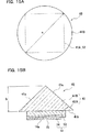
図9A及び図9Bは、第3の実施の形態に係る発光素子30の第1の構成例を示す。第1の構成例では、例えばサファイアなどの単一材料で形成された透光性基板31が正四角錐状を有し、その底面にn型半導体層13とp型半導体層14とを積層してなるダイオード構造12が設けられている。なお、透光性基板31の形状以外は上記第1の実施の形態の場合と同様である。
【0053】
透光性基板31を正四角錐状とすることにより、出射面31aとなる4つの斜面が、それぞれp型半導体層14の下面14aに対して傾斜しているので、上記第1の実施の形態で説明したように、光の取り出し効率を高めることができる。
【0054】
透光性基板31の底面31bの最大幅(すなわち底面31bの対角線寸法a)に対する高さbの比率(b/a)に応じて、出射面31aの傾斜角度が変化するので、底面31bの対角線寸法aに対する高さbの比率(b/a)を変化させることにより、光の取り出し効率を変化させることができる。図10は、上記比率(b/a)を変化させ、光の取り出し効率を求めた結果を示している。この結果から、比率(b/a)を約0.4以上で、かつ、約4.5以下に設定すれば、光の取り出し効率が約35%以上となり、従来の発光素子の光の取り出し効率(約22〜23%)に対して約1.5倍以上の値にすることができる。例えば、透光性基板31が正四角錐状であって、底辺の長さを350μm(すなわち対角線寸法aが495μm)、高さbを300μmとすると、対角線寸法aに対する高さbの比率が約0.6となり、光の取り出し効率の最高効率約37.5%が得られる。
【0055】
図11A及び図11Bは、第3の実施の形態に係る発光素子30の第2の構成例を示す。第2の構成例では、例えばサファイアなどの単一材料で形成された透光性基板31を円錐状としている。この場合、透光性基板31の底面31bに外接するように、n型半導体層13とp型半導体層14とを積層してなるダイオード構造12が設けられている。円錐状の透光性基板31の底面の直径aに対する高さbを上記正四角錐状の場合と同様に設定することにより、光の取り出し効率を向上させることができる。
【0056】
図12A及び図12Bは、第3の実施の形態に係る発光素子30の第3の構成例を示す。第3の構成例では、例えばサファイアなどの単一材料で形成された透光性基板31を略半球状(略球面状)としている。このように、透光性基板31を略半球状としても、出射面31aとなる球面がp型半導体層14の下面14aに対して傾斜するので、上記第1の実施の形態で説明したように、光の取り出し効率を高めることができる。
【0057】
透光性基板31の底面31bの最大幅(すなわち底面の直径c)に対する高さbの比率(b/c)に応じて、出射面31aの傾きが変化するので、底面31bの直径cに対する高さbの比率(b/c)を変化させることにより、光の取り出し効率を変化させることができる。図13は、上記比率(b/c)を変化させ、光の取り出し効率を求めた結果を示している。この結果から、上記比率(b/c)を約0.3以上に設定すれば、光の取り出し効率約35%が得られる。さらに、上記比率(b/c)を約0.5にすれば光の取り出し効率の最高効率約36%が得られることが判明した。例えば、ダイオード構造12の形状を一辺が350μmの正方形とし、ダイオード構造12が透光性基板31の底面31bに内接するように底面31bの直径cを設定すると、底面31bの直径cは約495μmとなる。透光性基板31の高さbを約165μmとすると、底面31bの直径cに対する高さの比率が約0.3となるので、従来の発光素子に比べて光の取り出し効率を十分高い値に設定することができる。
【0058】
表1は、ダイオード構造12のサイズを一辺が350μmの正方形とし、透光性基板31の形状及び高さbを変化させた場合の光の取り出し効率を光学シミュレーションにより求めた結果を示す。No.1〜No.3は、透光性基板31の形状を直方体形状(図55に示す、上面と下面とが平行な従来の透光性基板101と同等)とし、高さを変化させた場合のシミュレーション結果である。No.4〜No.9は、透光性基板31の形状を錐体状として高さを変化させた場合のシミュレーション結果である。また、No.10〜No.13は、透光性基板31の形状を略半球状(略球面状)として高さを変化させた場合のシミュレーション結果である。
【0059】
【表1】
表1から分かるように、透光性基板31の形状を直方体形状とした場合の光の取り出し効率が22%であるのに対して、錐体状とした場合の取り出し効率は最大で38%となり、光の取り出し効率を向上させることができる。また、透光性基板31の形状を半球形状とした場合の取り出し効率は最大で36%であるが、錐体状とした場合に比べて、透光性基板の高さを低くしても同程度の取り出し効率を得ることができる。
【0061】
なお、第3の実施の形態では、透光性基板31の形状を多角錐状、円錐状又は略半球状としたが、透光性基板31の形状をこれらに限定する趣旨のものではなく、例えば後述する図46Aに示す三角柱状(複数の傾斜面の組み合わせ)や図53に示すシリンドリカルレンズ状(略円筒面状)など、透光性基板の出射面がその入射面(底面)に対して非平行な形状であればよい。
【0062】
第4の実施の形態
次に、本発明の第4の実施の形態について説明する。上記第3の実施の形態では、サファイアなどの単一材料を多角錐状、円錐状又は略半球状に形成して透光性基板31としたが、第4の実施の形態では、透光性基板41が、サファイアなどで形成された平行板41Aと、平行板41Aの上面にエポキシ樹脂やシリコーン樹脂などの略透明で高屈折率の樹脂により多角錐状、円錐状又は略半球状(略球面状)の透光性部材41Bで構成されている。
【0063】
図14A及び図14Bは、第4の実施の形態に係る発光素子40の第1の構成例を示す。第1の構成例では、透光性基板41として、平行板41Aを、上面と下面が互いに平行で、かつ、水平方向の断面が正方形の略直方体とし、透光性部材41Bを正四角錐状としている。また、平行板41Aの底面にn型半導体層13とp型半導体層14とを積層してなるダイオード構造12が設けられている。
【0064】
図15A及び図15Bに示す第2の構成例では、透光性部材41Bを円錐状としている。また、図16A及び図16Bに示す第3の構成例では、透光性部材41Bを略半球状(略球面状)としている。
【0065】
第4の実施の形態によれば、加工の困難なサファイアを平行板とし、比較的加工が容易なエポキシ樹脂などを用いて透光性部材41Bを多角錐状、円錐状又は略半球状に形成しているので、製造工程が増加するものの、透光性基板41の加工コストを低減させることができる。
【0066】
表2は、上記表1と同じ条件で透光性部材41Bの形状及び高さbを変化させた場合の光の取り出し効率を光学シミュレーションにより求めた結果を示す。No.1〜No.3は、透光性基板41の透光性部材41Bの形状を直方体形状とし、高さを変化させた場合のシミュレーション結果である。No.4〜No.7は、透光性基板41の透光性部材41Bの形状を錐体状として高さを変化させた場合のシミュレーション結果である。また、No.8〜No.11は、透光性基板41の透光性部材41Bの形状を略半球状(略球面状)として高さを変化させた場合のシミュレーション結果である。
【0067】
【表2】
表2から分かるように、透光性部材41Bの形状を直方体形状とした場合の光の取り出し効率が23%であるのに対して、錐体状とした場合の取り出し効率は最大で38%となり、光の取り出し効率を向上させることができる。また透光性部材41Bの形状を略半球形状とした場合の取り出し効率は最大で36%であるが、錐体状とした場合に比べて、透光性基板の高さを低くしても同程度の取り出し効率を得ることができる。
【0069】
さらに、第4の実施の形態に係る発光素子40の変形例を図17及び図18に示す。これらの変形例は、発光素子40をフェースアップの状態で実装基板に実装するものであり、p型半導体層14の表面14aに、例えばエポキシ樹脂のような透明で高屈折率の樹脂を塗布することにより透光性部材42が設けられている。図17では、透光性部材42を多角錐状又は円錐状としている。また、図18では、透光性部材42を略半球状としている。
【0070】
表3は、上記変形例において、表1と同じ条件で透光性部材42の形状及び高さbを変化させた場合の光の取り出し効率を光学シミュレーションにより求めた結果を示す。No.1〜No.3は、透光性部材42の形状を直方体形状とし、高さを変化させた場合のシミュレーション結果である。No.4〜No.9は、透光性部材42の形状を錐体状として高さを変化させた場合のシミュレーション結果である。また、No.10〜No.13は、透光性部材42の形状を略半球状(略球面状)として高さを変化させた場合のシミュレーション結果である。
【0071】
【表3】
表3から分かるように、透光性部材42の形状を直方体形状とした場合の光の取り出し効率が23%であるのに対して、錐体状とした場合の取り出し効率は最大で31%となり、光の取り出し効率を向上させることができる。また透光性部材42の形状を略半球形状とした場合の取り出し効率は最大で31%であるが、錐体状とした場合に比べて、透光性基板の高さを低くしても同程度の取り出し効率を得ることができる。
【0073】
第5の実施の形態
次に、本発明の第5の実施の形態について説明する。上記第3及び第4の実施の形態では、透光性基板31又は41の全体が1つの多角錐状、円錐状又は略半球状に形成されているが、第5の実施の形態では、透光性基板51の出射面51aに複数の多角錐状、円錐状又は略半球状の凸部51aが形成されている。また、第2の実施の形態と比較すると、透光性基板の出射面に形成されている凸部の形状及び配列が規則的であるか否かが異なる。
【0074】
図19は、第5の実施の形態に係る発光素子50の第1の構成例を示す。第1の構成例では、透光性基板51の出射面51aに複数の、例えば正四角錐などの多角錐状又は円錐状の凸部51bが規則的に配列されている。その他の構成は、図4に示す第2の実施の形態の発光素子20又は図9A及び図9Bに示す第3の実施の形態の第1の構成例の発光素子30と同様である。
【0075】
個々の多角錐状又は円錐状の凸部51bに着目すると、上記第3の実施の形態での説明がそのまま当てはまるので、第3の実施の形態の場合と同様に、光の取り出し効率を従来の発光素子に比べて向上させることができる。また、個々の凸部51bの対角線寸法に対する高さの比率が、透光性基板の全体を1つの錐体とした場合と同じ比率であれば、対角線寸法が小さい分だけ凸部51bの高さが低くなる。その結果、発光素子50の全体の高さを低くすることが可能である。
【0076】
図20に示す第2の構成例では、透光性基板51が、サファイアなどで形成された平行板51Aと、エポキシ樹脂やシリコーン樹脂などの略透明で高屈折率の樹脂により形成された透光性部材51Bで構成されている。透光性部材51Bの出射面51aには、複数の多角錐状又は円錐状の凸部51bが規則的に配列されている。その他は第1の構成例と同様である。
【0077】
図21に示す第3の構成例では、発光素子50をフェースアップの状態で実装基板に実装したものであり、p型半導体層14の表面14aに、例えばエポキシ樹脂のような透明で高屈折率の樹脂により透光性部材52が設けられている。透光性部材52の出射面52aには、複数の多角錐状又は円錐状の凸部51bが規則的に配列されている。
【0078】
図22〜図24は、それぞれ上記第4〜第6の構成例を示し、第1〜第3の構成例とは、透光性基板51の出射面51a又は透光性部材52の出射面52aに規則的に配列された複数の凸部51b又は52bがそれぞれ略半球状に形成されている点が異なる。その他は、上記第1〜第3の構成例と同様である。
【0079】
第6の実施の形態
次に、本発明の第6の実施の形態について説明する。図25に示す第6の実施の形態の発光素子40’は、図16A及び図16Bに示す第4の実施の形態の第3の構成例の発光素子40において、透光性部材41Bと空気との界面での反射を防止するための反射防止膜42を形成したものである。反射防止膜42により、空気中への光の取り出し効率をさらに高くすることができる。なお、反射防止膜42以外の構成は第4の実施の形態の第3の構成例と同様であるため、その説明を省略する。
【0080】
反射防止膜42が形成されていない場合、透光性部材41Bと空気との界面で全反射が発生して損失が生じるが、本実施の形態では、透光性部材41Bの表面に、屈折率が約1.36のMgF2膜からなる反射防止膜42が単層コーティングされているので、透光性部材41Bと空気との界面で生じる反射損失が低減する。なお、反射防止膜42としては光学多層膜を利用したものでも良く、例えばTiO2とSiO2とAL2O3の積層膜で反射防止膜42を構成してもよい。
【0081】
なお、本実施の形態は、第4の実施の形態の発光素子40の出射面41aに反射防止膜42が形成されているが、他の実施の形態に係る発光素子の出射面に反射防止膜を形成しうることは言うまでもない。
【0082】
第7の実施の形態
次に、本発明の第7の実施の形態について説明する。上記第1から第6の実施の形態に係る発光素子では、透光性基板の非出射面側に単一のn型半導体層13及びp型半導体層14を積層してダイオード構造12を形成したが、図26に示す第7の実施の形態に係る発光素子40”では、複数の部分にn型半導体層13及びp型半導体層14が積層されており、事実上ダイオード構造12が複数の部分に分割されている。なお、それ以外の構成は上記第4の実施の形態の第3の構成例と同様であるため、その説明を省略する。また、図示を省略しているが、n型半導体層13及びp型半導体層14の下面にはそれぞれバンプ電極が形成されており、バンプ電極を用いて実装基板にフェースダウンの状態で実装されている。
【0083】
第7の実施の形態に係る発光素子40”のようにダイオード構造12が複数に分割された構造では、分割された各部分にそれぞれバンプ電極が設けられ、実装基板に接続されるので、事実上熱伝導経路が増える。その結果、発光素子で発生した熱の放熱性が向上し、発光素子40”の寿命を長くすることが可能となる。また、発光時における発光素子40”の温度が低くなるので、発光素子40”から放射される光量が増加する。さらに、バンプ電極1対あたりのn型半導体層13及びp型半導体層14の面積が狭くなるため、分割された各部分での電流密度分布がより均一化され、輝度むらが低減される。
【0084】
なお、本実施の形態では、第4の実施の形態の発光素子40のダイオード構造12を複数に分割しているが、他の実施の形態に係る発光素子のダイオード構造12を複数に分割しうることは言うまでもない。
【0085】
また、図27に示すように、1つの比較的大きな透光性部材51の下面(光の入射面)に密着するように、例えば図55に示す従来の発光素子100と同様の構成の発光部62を複数個密着するように配置してもよい。このように、光の出射面が入射面に対して非平行な透光性部材61に任意の数の発光部62を密着配置させることにより、目的に応じて任意の発光面積を有する発光素子60を提供することができる。また、透光性部材61の存在により、単に従来の発光素子100を複数個配列した場合よりも光の取り出し効率を高くすることができる。
【0086】
第8の実施の形態
次に、本発明の第8の実施の形態について説明する。上記第1から第7の実施の形態は、それぞれ発光素子に関するものであったが、第8の実施の形態は、上記いずれかの発光素子を用いた発光装置に関する。
【0087】
第8の実施の形態に係る発光装置200の構成を図28に示す。発光装置200は、発光素子201を実装するための凹部202が形成された実装基板203と、凹部202と対向する位置(発光素子201の光の出射面の前方)に蛍光部材204が設けられた光学部材205などで構成されている。
【0088】
発光素子201は、例えば青色光を放射する青色発光素子であり、上記第1から第8の実施の形態に係る発光素子のいずれの構成であってもよい。発光素子201をフェースダウン実装する場合は、例えば図1において符号16a及び16bで示されたバンプ電極を介して実装基板203の回路に電気的に接続されている。
【0089】
蛍光部材204は、例えば青色光により励起されて黄色を発光する蛍光体を含み、光学部材205に形成された凹部207に、上記蛍光体を含む樹脂が充填されることにより形成されている。蛍光部材204は、上記のように発光素子201に対向するように配置されており、かつ発光素子201から放射される光束の大部分が入射するようにその大きさが設定されている。光学部材205は、例えばアクリル樹脂などの透光性材料で形成されており、蛍光体204とは反対側には、配光を制御するために、所望する形状の凸レンズ206などが形成されている。
【0090】
発光素子201から放射された青色光は、蛍光部材204に入射し、その一部が蛍光体を励起して、入射した青色光とは波長の異なる光を発生させる。そして、蛍光部材204を透過した青色光と、蛍光体により発生された光とが混合されることにより、例えば白色光が発光装置200から出力される。
【0091】
なお、発光素子201が紫外線を放射する発光素子の場合でも、蛍光体の種類を適宜選択することにより、蛍光体による励起光の混合により白色光を出力することができる。
【0092】
このように、光学部材205内において蛍光部材204を発光素子201に最も近い位置に配置することにより、発光素子201から放射された光束を有効に蛍光部材204に入射させることができる。また、発光素子202とは別部材である光学部材205が所定の光学形状に形成されると共に、光学部材205に蛍光部材204が設けられているので、発光素子201への応力、熱、化学的負荷が低減される。
【0093】
さらに、蛍光部材204を発光素子201と接しないように、両者の間に適当な隙間を設けることにより、蛍光部材204が発光素子201からの熱に直接曝されることがなくなり、蛍光体や蛍光体を含む樹脂などの劣化が低減される。その結果、蛍光部材204の寿命を延ばすことができ、これによって光束減退が抑えられ、発光装置200の寿命を延ばすことが可能となる。さらに、蛍光部材204と発光素子201とが接していないので、発光素子201の放熱性も良好になる。
【0094】
さらに、劣化の早い蛍光体や蛍光体を含む樹脂などの蛍光部材204が光学部材205側に設けられ、かつ光学部材205が実装基板203に対して着脱自在であるので、蛍光部材204の劣化により発光装置200の発光特性が劣化した場合には、光学部材205を新しいものに交換することにより、蛍光部材204を更新することができる。その結果、発光装置200の発光特性を初期状態に回復させることができる。
【0095】
第8の実施の形態に係る発光装置の変形例を図29に示す。図29から明らかなように、この変形例では、1つの実装基板203上に複数の凹部202が形成され、各凹部202にそれぞれ発光素子201が実装されていると共に、1つの光学部材205上に各凹部202と対向する複数の蛍光部材204及びレンズ206が設けられている。このような変形例により、上記と同様の効果を有し、かつ、発光部の面積を大きくした面発光装置が得られる。
【0096】
図30に示す第8の実施の形態の別の変形例では、蛍光部材204の発光素子201側の面が、実装基板203に形成された凹部202の開口と略等しい大きさに形成されている。具体的には、光学部材205の凹所207の開口縁と実装基板203の凹部202の開口縁を略同じ形状にして、両者を合致させている。上記の凹所207に蛍光体を含む樹脂を充填すると、蛍光部材204の発光素子201側の面が凹部202の開口面と略等しい大きさとなる。
【0097】
この変形例の場合、実装基板203及び光学部材205の寸法精度が要求されるものの、蛍光部材204の大きさを必要最小限にすることができ、できるだけ小さな疑似光源が得られる。その結果、光学部材205の凸レンズ206の光学形状を適宜選択することにより配光制御が容易になり、所望の配光分布を実現することが可能となる。さらに、蛍光部材204の発光素子201側の面が凹部202の開口と略等しい大きさに形成されているので、蛍光部材204での発光部分の輪郭のぼやけがなくなり、配光特性が良好となる。
【0098】
次に、第8の実施の形態のさらに別の変形例を図31に示す。この変形例の発光装置200’は、実装基板203の凹部202に複数の発光素子201が近接させて実装されたものである。これに伴い、実装基板203の凹部202及び光学部材205の蛍光部材204も大型化されている。この変形例の場合、複数の発光素子201が用いられているので、発光素子200全体の輝度が高くなると共に、各発光素子201が蛍光部材204の中央部に対向するように配置されているので、蛍光部材204における発光も中心部が高輝度となり、より点光源化できるため、狭角配光特性を実現することができる。
【0099】
第9の実施の形態
次に、本発明の第9の実施の形態について説明する。第9の実施の形態に係る発光装置210の構成を図32に示す。発光装置210は、発光素子201が実装された実装基板203と蛍光部材204が設けられた光学部材211で構成され、実装基板203は上記第9の実施形態に係る発光装置200と同様である。
【0100】
光学部材211は、蛍光部材204により波長変換されて放射された光束のうち、光学部材211の光取出し面212に向かう方向とは異なる方向に放射された光束を、光取出し面212に向かう方向に反射させるように構成されている。具体的には、光学部材211の光取出し面212とは反対側の面213の発光素子201と対向する箇所に凹部214が形成され、凹部214に蛍光体を含む樹脂が充填されて蛍光部材204が形成されている。蛍光部材204の両側部には、蛍光部材204から光取り出し面212とは異なる方向に放射された光束を光取出し面212に向かう方向に全反射させるための傾斜面215が形成されている。なお、光取り出し面212は、実装基板203の上面208に対して平行に形成されている。
【0101】
通常、蛍光部材204から放射された光束は、図31において矢印Aで示すように直接光取出し面212へ向かうものと、矢印Bで示すように光取出し面212へ向かわずに略横方向へ向かうものに分かれる。蛍光部材204から略横方向に放射された光束は、傾斜面215で反射され、光取り出し面212から外部に放射される。その結果、発光装置210から放射される光を所定の方向へ配光制御することができる。
【0102】
なお、図33に示すように、傾斜面215及び光取り出し面212の背面216にアルミ蒸着などによる反射部217を設けてもよい。その場合、光学部材211の光取出し面212とは反対側の面213のうち、少なくとも発光素子201から放射された光束が入射する部分には、反射部を形成しないことは言うまでもない。このように、傾斜面215及び光取り出し面212の背面216に反射部217を設けることにより、傾斜面215及び光取り出し面212の背面216に入射した光束を全て反射させることができ、これらの面から実装基板203側に光束が漏れるのを防止することができ、発光効率をさらに向上させることができる。また、反射部217は、光学部材211と実装基板203の間に設けられるので、容易に触れることができず、反射部の劣化や汚れを少なくすることができる。
【0103】
第10の実施の形態
次に、本発明の第10の実施の形態について説明する。第10の実施の形態は、実装基板203に発光素子201が実装されるための凹部202に関するものである。光学部材については、上記第8の実施の形態及び第9の実施の形態のいずれの形状であってもよく、また、これら以外の形状のものであってもよい。
【0104】
図34に示す第10の実施の形態の第1の構成例では、実装基板203に設けられた凹部202の内周面が、略放物面形状に形成されている。このような構成により、発光素子201から放射された一部の光束は、凹部202の略放物面形状の内周面で反射され、図34中矢印で示すように、蛍光部材204に略平行光として入射される。その結果、蛍光部材204へ入射する光量を多くすることができると共に、蛍光部材204における発光輝度分布を均一化することができる。その結果、発光装置の光取り出し面における色むらを抑えることができる。
【0105】
図35に示す第10の実施の形態の第2の構成例では、実装基板203に設けられた凹部202の内周面が、略楕円面形状に形成されている。このような構成により、発光素子201から放射された一部の光束は、凹部202の略楕円面形状の内周面で反射され、図35中矢印で示すように、蛍光部材204の中心を向くように入射される。その結果、蛍光部材204へ入射する光量を多くすることができると共に、蛍光部材204の中心部へ光束を集中させることができ、蛍光部材204サイズを小さくすることができる。その結果、より点光源化することができるため、狭角配光特性を実現することができる。
【0106】
第11の実施の形態
次に、本発明の第11の実施の形態について説明する。第11の実施の形態は、実装基板203の凹部202に発光素子201を固定する方法に関する。
【0107】
図36に示す第11の実施の形態の第1の構成例では、発光素子201として、例えば図16A及び図16Bに示す第4の実施の形態に係る発光素子40の第3の構成例と同様のものが用いられている。図16Bに示す発光素子40は、略半球状の透光性部材41Bを除くと、図55に示す従来の発光素子100と同様の構成である。
【0108】
そこで、第1の構成例における発光素子201は、従来例と同様の構成を有する発光部62に、例えばアクリル樹脂などの透光性高屈折率材料を用いて形成された略半球状の透光性部材42を接着することにより形成されている。まず、実装基板203の凹部202に発光部62を実装する。次に、凹部202にシリコーン樹脂などの比較的屈折率の高い透光性の樹脂230を半充填し、その状態で発光部62の出射面上に透光性部材42を密接するように設置させて、透光性部材の側面下部が浸かる状態で固定している。そのため、予め発光部62に透光性部材42を固定して発光素子201を組み立てておき、組み立てた発光素子201を実装基板203に実装するよりも、発光素子201の実装が容易になる。また、透光性部材42と発光部62との隙間に樹脂が侵入するため、透光性部材42と発光部62の密着性が向上し、かつ強固に固定される。さらに、発光素子201の側部が比較的屈折率の高い樹脂で覆われるため、発光素子201の側部からの光の取り出し効率も向上する。
【0109】
また、透光性部材42の材料として、凹部230に充填される樹脂(例えばシリコーン樹脂)と同じ材料を用いた場合、事実上界面が1つ減るため、フレネル反射によるロスを少なくすることができる。また、透光性部材42と発光部62の界面での密着性が向上するので、界面での光の取り出し効率が向上すると共に、透光性部材42を固定する強度も向上する。
【0110】
図37に示す第11の実施の形態の第2の構成例では、透光性部材42と発光部62の間に、透光性部材42の材料の屈折率n2と発光部62の透光性基板(例えば図55の透光性基板101参照)の材料の屈折率n0の中間の屈折率n1を有する材料からなる透光性中間層231を設け、凹部202にシリコーン樹脂などの比較的屈折率の高い透光性の樹脂230を半充填して透光性部材42を固定している。例えば、発光部62の透光性基板の材料をサファイア(屈折率n0=1.77)とし、透光性部材42の材料をアクリル(屈折率n2=1.49)とすると、1.77>n1>1.49の条件を満たす材料で透光性中間層231を形成すればよい。その場合、透光性部材42は樹脂230により固定されるので、透光性中間層231の材料は必ずしも接着性を有している必要はない。
【0111】
次に、透光性中間層231の屈折率n1を透光性部材42の材料の屈折率n2と発光部62の透光性基板の材料の屈折率n0の中間の値とする理由について説明する。なお、屈折率n0、n1、n2に関しては、上記従来例に関する説明を参照するので、同じ符号を重複して使用している。
【0112】
従来例の説明で述べたように、屈折率n0、n1、n2(n0>n1>n2)を有する3層が順に積層されている場合、屈折率n0の第1層から屈折率n2の第3層への光の臨界角θ0は、第2層の屈折率n1とは無関係に、θ0=sin−1(n2/n0)となる。この場合、第1層である発光部62の透光性基板の材料がサファイア(n0=1.77)であり、第3層である透光性部材42の材料がアクリル(n2=1.49)であるので、臨界角θ0=sin−1(n2/n0)≒57度(式1)となる。
【0113】
一方、屈折率n0、n1、n2(n0>n2>n1)を有する3層が順に積層されている場合、屈折率n1の第2層と屈折率n2の第3層との界面では全反射は起こらず、屈折率n0の第1層から屈折率n1の第2層に入射した光は全て屈折率n2の第3層に入射する。従って、屈折率n0の第1層から屈折率n2の第3層への光の臨界角θ0は、第1層の屈折率n0と第2層の屈折率n1に支配され、θ0=sin−1(n1/n0)(式2)となる。その場合、臨界角θ0は、第2層の屈折率n1が小さくなるほど小さくなる。
【0114】
透光性中間層231の屈折率n1と臨界角θ0の関係を図38に示す。図38から分かるように、透光性中間層231の屈折率n1を透光性部材42の材料の屈折率n2よりも大きくすれば、透光性部材42中に入射する光量が最大になる。一方、一般的に屈折率の大きな材料は高価であること及びフレネル反射による損失が大きいことを考慮すると、屈折率n1は小さい方が好ましい。従って、上記のように透光性中間層231の屈折率n1を透光性部材42の材料の屈折率n2と発光部62の透光性基板の材料の屈折率n0の中間の値とすることにより、発光部62から出射された光を、最も効率良く透光性部材42に入射させることができる。
【0115】
図39に示す第3の構成例では、透光性部材42の底部近傍において光の出射面か外側に突出するように鍔42aを設け、鍔42aが樹脂230中に完全に埋設されるように、樹脂230を凹部202に充填する。このような構成により、第1の構成例と比較して、透光性部材42の形状が若干複雑になるものの、樹脂230との接触面積が増え、透光性部材42を固定するための機械的強度が向上する。また、上記第2の構成例のように、透光性部材42の材料の屈折率と発光部62の透光性基板の材料の屈折率の中間の屈折率を有する透光性中間層を設けてもよい。
【0116】
第12の実施の形態
次に、本発明の第12の実施の形態について説明する。第12の実施の形態は、複数の発光素子を用いた面発光照明装置に関するものである。第12の実施の形態に係る面発光照明装置300の第1の構成例を図40に示す。面発光照明装置300の第1の構成例では、複数の発光素子301が実装基板302上に実装されており、実装基板302は筐体303の略中央部に保持されている。また、蛍光体を含む材料で形成された平板状の蛍光部材304が、実装基板302の実装面と略平行となるように筐体303の上端近傍に保持されている。
【0117】
発光素子301は、上記第3又は第4の実施の形態に係る多角錐状又は円錐状の透光性基板又は透光性部材を有する発光素子であり、例えば青色光又は紫外線を放射する。また、発光素子301は、図示した形状のものに限定されず、上記第1から第7の実施の形態に係る各発光素子のうち、光の出射面の所定方向の断面が発光素子の発光面であるpn接合面15から離れるにつれて幅が狭くなるように形成されているものであればよい。
【0118】
発光素子301は、実装基板302上にそれぞれの間隔が略均等になるように配列されている。実装基板302上には、各発光素子301が、それぞれ電気的に直列に接続されたものが複数組並列に接続されるように、配線パターンが形成されている。筐体303は、例えば金属や樹脂などにより有底の略円筒状に形成されたものであり、例えば高さ約20mm程度で、直径が約50mm程度である。実装基板302は、筐体303の側壁303aの中央部近傍において、側壁303aに対して略直交するように固定されている。蛍光部材304は、例えばアクリルなどの透光性材料に蛍光体を混入したものを用いて円盤状に形成され、実装基板302の実装面に対して約5mm程度の間隔を設けるように、筐体303の側壁303aの上端近傍において、側壁303aに対して略直交するように固定されている。
【0119】
このように、実装基板302上に配列された複数の発光素子301から青色光又は紫外線を放射し、青色光又は紫外線により蛍光部材304の蛍光体が励起されて波長の異なる光を放射することにより、面発光照明装置300の発光面304aから白色光が略均一に出力される。
【0120】
次に、多角錐状又は円錐状の透光性基板又は透光性部材を有しない従来の発光素子(例えば図55の発光素子100参照)の配光分布を図41に示す。図41から分かるように、多角錐状又は円錐状の透光性基板又は透光性部材を用いない場合、略完全拡散配光となる。図42に示すように、鉛直軸(0°の軸)方向に放射される光の強度をI0とし、鉛直軸に対する時計方向の角度をθとすると、θ方向に放射される光の強度はI0cosθとなる。鉛直軸に対して任意の角度αの範囲から放射される光束φは、
【0121】
【数1】
【0122】
このような配光特性を有する発光素子を実装基板302上に配列すると、発光装置の発光面である蛍光部材における発光素子301の上方の輝度が高く、また発光素子301の間の輝度が相対的に低くなり、輝度分布が不均一となる。
【0123】
次に、頂角が20°、40°及び60°の円錐状の透光性基板又は透光性部材を有する発光素子の配光分布を、それぞれ図43、図44及び図45に示す。各図中の実線と破線は、それぞれ90°異なる断面の配光を示すものである。発光素子から出射された光束は、頂角を形成する面、すなわち光の出射面で幾度か反射を繰り返し、次第に頂角を形成する面に対する入射角を大きくしながら、頂角を形成する面から出射される。このように、円錐状の透光性基板又は透光性部材を設けることにより、発光素子上方への光束が低減され、その分角度のついた方向の成分が増加した配光となる。具体的には、円錐状の透光性基板又は透光性部材を設けない場合には、相対光度のピークがθ=0°の時であったが、頂角20°の円錐状の透光性基板又は透光性部材を設けた場合には、相対輝度のピークがθ=45°、315°となる。また、円錐状の透光性基板又は透光性部材による配光は、頂角が小さいほど広角配光となる。
【0124】
このように、円錐状の透光性基板又は透光性部材を発光素子301に設けることにより、発光素子301から出射された光束が広角に配光されて蛍光部材304に入射するので、蛍光部材304の発光面304aにおける輝度の均一性が向上する。
【0125】
なお、透光性基板又は透光性部材の形状は、円錐状に限られず、多角錐状やその他の形状であってもよい。図46Aは、三角柱状の透光性基板又は透光性部材310を用いた発光素子301’を示す。また、この発光素子301’の配光分布を図47に示す。図47中、実線は断面形状が三角形の方向の配光分布を示し、破線は断面形状が長方形の方向の配光分布を示す。このような三角柱状の透光性基板又は透光性部材310を用いることによっても、発光素子301’の発光部から出射された光を広角に配光することができる。
【0126】
また、発光部62は、実装基板(図示せず)側にダイオードが形成されたフェースダウン実装であってもよいし、逆に透光性基板又は透光性部材310側にダイオードが形成されたフェースアップ実装であってもよい。
【0127】
このような発光素子301を図40に示す面発光照明装置300の実装基板302に実装することによっても、発光素子から出射された光束が広角に配光されて蛍光部材304に入射するので、蛍光部材304の発光面304aにおける輝度の均一性が向上する。
【0128】
さらに、図46Bに示すように、1つの三角柱状の透光性基板又は透光性部材310の矩形の入射面に複数の発光部62を配置してもよい。その場合、透光性基板又は透光性部材310が比較的大きくなり、成形及び取り扱いが容易になると共に、面発光装置300の全体としての部品点数を削減することができる。
【0129】
次に、第12の実施の形態に係る面発光照明装置300の第2の構成例を図48に示す。面発光照明装置300の第2の構成例では、上記第1の構成例に加えて、実装基板302と蛍光部材304の間に、例えばアクリル樹脂で成形された導光部材305が設けられている。導光部材305の実装基板302側の面の発光素子301に対向する位置には、発光素子301の透光性基板又は透光性部材310と同様の形状の凹部305aが形成されており、その凹部305aに各発光素子301の透光性基板又は透光性部材310の少なくとも先端部分(好ましくは、略全体)が挿入されている。また、導光部材305の実装基板302側の面のうち凹部305aが形成されていない部分305bには、拡散反射を目的として微細加工又はシルクスクリーン印刷による白色ドットパターンが施されている。さらに、導光部材305の端面305cには鏡面処理が施されている。
【0130】
このような第2の構成例において、発光素子301から透光性基板又は透光性部材310を介して出射された光束は、その大部分が略同一角度で導光部材305の凹部305aに入射する。導光部材305に入射した光のうち、導光部材305の出射面305dに対して臨界角よりも入射角の大きな光束は導光部材305の内部で反射が繰り返される。その過程で導光部材305の拡散反射処理が施された面305bで拡散反射されるので、最終的に出射面305dから出射される。このように、各発光素子301から出射された光は、導光部材305中を導光されることにより、ある程度均一化されて蛍光部材304に入射するので、蛍光部材304の発光面304aにおいて輝度の均一性を向上させることができる。
【0131】
次に、図49に示すように、発光素子301の透光性基板又は透光性部材310の頂角γ2(=40°)とし、導光部材305の凹部305aの開き角γ1として、開き角γ1を変化させた場合において、導光部材305の内部で反射されずに直接出射される光の割合を図50に示す。図50から分かるように、導光部材305の凹部305aの開き角γ1が小さいほど、導光部材305から直接出射される光束の割合が小さくなり、導光部材305の内部で繰り返し反射される光束の割合が大きくなる。導光部材305の凹部305aの開き角γ1を発光素子301の透光性基板又は透光性部材310の頂角γ2(40°)よりも小さくすれば、導光部材305に入射した光束のうち80%以上が導光部材305の内部で反射される。その結果、面発光照明装置300の発光面304aの輝度をより均一にすることができる。
【0132】
さらに、導光部材305を用いることにより、図41に示す第1の構成例と比較して、部品点数が増加するものの、導光部材305内での導光作用により、蛍光部材への照射密度を均一化できるため、発光素子の数を減らすか、あるいは設置間隔を大きくしても蛍光部材での輝度分布を均一にすることができる。
【0133】
第13の実施の形態
次に、本発明の第13の実施の形態について説明する。第13の実施形態は、発光素子を導光部材の側面に配置した面発光照明装置に関するものである。図51は第13の実施の形態に係る面発光照明装置400の平面断面図であり、図52はその正面断面図である。
【0134】
各図から分かるように、略円盤状の導光部材405の略円筒状側面のうち平面状に形成された部分を入射面405aとし、入射面405aに対向するように実装基板402及び実装基板402に実装された複数の発光素子401が配置されている。導光部材405の底面405bには、複数の発光素子401から遠ざかるに従って、密となるように微細加工や白色ドットパターンなどの拡散反射処理が施されている。さらに、導光部材405の出射面405cに対して所定の間隔を開けて、蛍光体を含む材料で形成された蛍光部材404が配置されている。
【0135】
発光素子401の透光性基板又は透光性部材410は、例えば図53に示すようにシリンドリカルレンズ状(略円筒面状)に形成され、発光部62が透光性基板又は透光性部材410の略長方形の底面に密着するように接合されている。また、図51に示すように、発光素子401は、その透光性基板又は透光性部材410の略半円形断面が導光部材405の略円形断面と直交方向となるように実装基板402上に実装されている。
【0136】
シリンドリカルレンズ状の透光性基板又は透光性部材410を有する発光素子401の配光分布を図54に示す。図54中、実線は略半円形断面方向の配光分布を示し、破線は略長方形断面方向の配光分布を示す。発光素子401の配光は、略半円形断面方向では比較的狭角な配光となり、略長方形断面方向では広角な配光となる。
【0137】
なお、複数の発光部62を1つのシリンドリカルレンズの下面に1列に配置しても同様の効果が得られる。
【0138】
従って、発光素子401から出射された光は、シリンドリカルレンズ状の透光性基板又は透光性部材410により、導光部材405の厚み方向には狭角に配光され、導光部材405の平面に平行な方向には広角に配光される。この場合、導光部材405の厚み方向への光束の入射角度は小さいので、導光部材405の底面505b及び出射面405cで全反射する成分が増加する。
【0139】
このように、導光部材405の側面に発光素子401を配置しても、導光部材405の全域に光束を導光させることができ、面発光照明装置400の蛍光部材404の発光面404aの輝度を均一にすることができる。また、発光素子401を導光部材405の側部に配置しているので、発光素子401の取り替えなどの保守が容易となる。
【0140】
また、シリンドリカルレンズ状の透光性基板又は透光性部材410の非長方形の断面は、略半円形に限定されず、略半楕円形やその他任意の曲面であってもよい。
【0141】
さらに、上記全ての実施の形態の特徴は、フェースダウン実装及びフェースアップ実装のいずれのタイプの発光素子にも適用しうることは言うまでもない。
【0142】
本願は日本国特許出願2002−154262、2002−218891及び2002−218989に基づいており、その内容は、上記特許出願の明細書及び図面を参照することによって結果的に本願発明に合体されるべきものである。
【0143】
また、本願発明は、添付した図面を参照した実施の形態により十分に記載されているけれども、さまざまな変更や変形が可能であることは、この分野の通常の知識を有するものにとって明らかであろう。それゆえ、そのような変更及び変形は、本願発明の範囲を逸脱するものではなく、本願発明の範囲に含まれると解釈されるべきである。【Technical field】
[0001]
The present invention relates to a light-emitting element with improved light extraction efficiency, a light-emitting device using the same, and a surface-emitting illumination device.
[Background]
[0002]
The structure of a conventional non-sealing light emitting element is shown in FIG. A conventional non-sealing type
[0003]
The
[0004]
The light beam C1 totally reflected by the
[0005]
When the material of the n-
[0006]
As described above, the light beam emitted from the conventional
[0007]
Therefore, conventionally, in order to improve the light extraction efficiency into the air, the periphery of the light-emitting
[0008]
Thus, when the periphery of the light-emitting
[0009]
For example, when the surface of the diode structure and the surface of the translucent resin layer are substantially parallel, the refractive index of the substance constituting the diode structure is expressed as n.0, The refractive index of the translucent resin layer is n1, The refractive index of the outer medium is n2And the critical angle at the interface between the diode structure and the translucent resin layer in the case of total reflection at the interface between the translucent resin layer and the outer medium is θ0The critical angle at the interface between the translucent resin layer and the outer medium is θ1Then the critical angle θ0, Θ1Is expressed as:
θ0= Sin-1(N1/ N0)
θ1= Sin-1(N2/ N1)
Where n0× sinθ0= N1× sinθ1Because the relationship
sinθ0= (N1/ N0) × sinθ1
= (N1/ N0) X sin (sin-1(N2/ N1))
= (N1/ N0) X (n2/ N1) = N2/ N0
It becomes.
[0010]
Therefore, the critical angle of the light beam emitted from the diode structure to the outer medium is sin.-1(N2/ N0) That is, the critical angle θ when the diode structure is not sealed with a translucent resin layer0Is represented by the same formula. When the surface of the diode structure and the surface of the translucent resin layer are substantially parallel, the critical angle depends only on the refractive index of the material constituting the diode structure and the refractive index of air, and is sealed with the translucent resin layer. Even if stopped, the light extraction efficiency cannot be improved.
[0011]
On the other hand, the light-transmitting resin layer is enlarged so that the light-emitting element can be regarded as a point light source, and the light exiting surface of the light-transmitting resin layer is incident substantially perpendicular to the light exiting surface. Is formed in a substantially spherical shape, the total reflection at the interface between the translucent resin layer and the outer medium can be minimized to maximize the luminous flux emitted into the air. In this case, the light extraction efficiency into the air is about 35 to 40% of the luminous flux generated at the pn junction surface.
[0012]
As described above, in the conventional unsealed light emitting element, the light extraction efficiency into the air is very small. On the other hand, in a sealed light-emitting element sealed with a light-transmitting resin, the light extraction efficiency into the air is improved, but the light-emitting element (light-emitting portion) is covered with a light-transmitting resin layer having a low thermal conductivity. Therefore, the heat generated in the light emitting element is dissipated only by being conducted to the outside through the electrode or the lead wire, the heat dissipation is poor, and the life of the light emitting element is reduced.
[0013]
In addition, when the emission color of the light-emitting element is blue or ultraviolet light, the light flux density in the short wavelength region is large, so that the light-transmitting resin layer that seals the light-emitting portion is easily deteriorated, and the life of the light-emitting element is reduced. Furthermore, since the size of the translucent resin layer for sealing the light emitting element is much larger than that of the light emitting element, the entire light emitting element is increased in size and the material cost is increased.
DISCLOSURE OF THE INVENTION
[0014]
The present invention has been made in order to solve the above-described problems of the conventional light emitting device, and achieves the longest life of the non-encapsulated light emitting device, while at the highest level among the light emitting devices having the conventional sealed structure. An object of the present invention is to provide a light emitting element capable of obtaining light extraction efficiency equivalent to that of a light emitting device, a light emitting device using the light emitting device, and a surface emitting illumination device.
[0015]
The invention according to
The surface of the translucent substrate facing the surface where the diode structure is formed is non-parallel to the surface of the diode structure opposite to the translucent substrate,
The diode structure and the translucent substrate are mounted on a bottom surface of a recess formed in a mounting substrate, and the transparent substrate is transparent to the surface opposite to the diode structure. It is characterized by being filled with a photo-resin.
[0016]
According to a second aspect of the present invention, in the light-emitting element according to the first aspect, the surface of the translucent substrate that faces the surface on which the diode structure is formed is an inclined surface, a rough surface, a substantially conical shape, It has a substantially spherical shape, a surface on which a plurality of substantially cone-shaped or substantially spherical convex portions are arranged, a combination of a plurality of inclined surfaces, or a substantially cylindrical surface shape.
[0017]
According to a third aspect of the present invention, in the light emitting device according to the second aspect of the present invention, a surface of the translucent substrate that faces the surface on which the diode structure is formed has a substantially cone shape, and the substantially cone shape. The ratio of the height to the maximum width of the bottom surface of the portion is about 0.4 or more and about 4.5 or less.
[0018]
According to a fourth aspect of the present invention, in the light-emitting element according to the second aspect, the surface of the translucent substrate that faces the surface on which the diode structure is formed is substantially spherical, and the substantially spherical portion. The ratio of the height to the diameter of the bottom surface is about 0.3 or more and about 0.5 or less.
[0019]
According to a fifth aspect of the present invention, in the light emitting device according to the first aspect, the translucent substrate is formed of a first material and is parallel to the first surface and the first surface on which the diode configuration is formed. A parallel plate having a second surface, a third surface formed of a second material and joined to the second surface of the parallel plate, and a translucent member having a fourth surface facing the third surface. The diode structure is formed on the first surface, and the fourth surface of the translucent member is non-parallel to the first surface.
[0020]
According to a sixth aspect of the present invention, in the light emitting device according to the fifth aspect, the fourth surface of the translucent member is an inclined surface, a rough surface, a substantially conical shape, a substantially spherical shape, or a plurality of substantially conical shapes. Alternatively, it is characterized in that it has a surface on which substantially spherical convex portions are arranged, a combination of a plurality of inclined surfaces, or a substantially cylindrical surface shape.
[0021]
The invention according to claim 7 is a light emitting device mounted on a mounting substrate, and is provided in front of the light emitting device, is excited by light emitted from the light emitting device, and emits light having a wavelength different from the excitation wavelength. A light emitting device including a fluorescent member,
The light emitting device has a diode structure formed by stacking an n-type semiconductor layer and a p-type semiconductor layer on one surface of a light-transmitting substrate,
The surface of the translucent substrate facing the surface where the diode structure is formed is non-parallel to the surface of the diode structure opposite to the translucent substrate,
The diode structure and the translucent substrate are mounted on a bottom surface of a recess formed in a mounting substrate, and the transparent substrate is transparent to the surface opposite to the diode structure. Filled with photo-resin,
The surface of the fluorescent member facing the light emitting element is approximately the same size as the opening of the recess.
[0022]
According to an eighth aspect of the present invention, in the light emitting device according to the seventh aspect, an optical member having the fluorescent member on a surface or inside thereof is detachably mounted on the mounting substrate.
[0023]
The invention according to claim 9 is the light emitting device according to claim 7, wherein the optical member has a convex lens shape.
[0024]
According to a tenth aspect of the present invention, in the light emitting device according to the seventh aspect, the inner peripheral surface of the concave portion is formed in a substantially parabolic surface or a substantially elliptical surface, and the light emitted from the light emitting element is transmitted in the concave portion. It is made to enter into the said fluorescent member by reflecting on a surrounding surface.
[0025]
According to an eleventh aspect of the present invention, in the light emitting device according to the seventh aspect, the member having a surface functioning as a light emitting surface of the light emitting element and the translucent resin filled in the concave portion are made of the same material. It is characterized by being.
[0026]
The invention according to
[0027]
The invention according to
[0028]
The invention according to
The light emitting device has a diode structure formed by stacking an n-type semiconductor layer and a p-type semiconductor layer on one surface of a light-transmitting substrate,
The surface of the translucent substrate facing the surface where the diode structure is formed is non-parallel to the surface of the diode structure opposite to the translucent substrate,
The diode structure and the translucent substrate are mounted on a bottom surface of a recess formed in a mounting substrate, and the transparent substrate is transparent to the surface opposite to the diode structure. It is characterized by being filled with a photo-resin.
[0029]
The invention according to
[0030]
The invention according to claim 16 is the surface-emitting illuminating device according to
[0031]
The invention according to
[0032]
According to an eighteenth aspect of the present invention, in the surface emitting illumination device according to the fifteenth aspect, the diode structure of the light emitting element is located at a position facing each light emitting element on the surface of the light guide member facing the light emitting element. A recess having substantially the same shape as the surface facing the formed surface is formed, and at least a part of the surface facing the surface where the diode structure of the light emitting element is formed is inserted into the recess. It is characterized by.
[0033]
The invention according to claim 19 is the surface-emitting illuminating device according to
[0034]
According to the light emitting device of the first aspect of the present invention.In the case of a conventional light emitting device, the total reflection is repeated between the light emitting surface of the light emitting device and another surface, and the light flux absorbed by the material constituting the light emitting device is repeatedly subjected to total reflection. The incident angle of the light on the light exit surface gradually decreases, becomes smaller than the critical angle, and is emitted to the outside from the light exit surface. As a result, the extraction efficiency of light emitted from the light emitting element to the outside can be improved. As a result, even if it is an unsealed light emitting element, the light extraction efficiency equivalent to the highest level among the conventional sealed light emitting elements can be obtained. Further, since the light-emitting element is not sealed with resin, the light-emitting element itself can be reduced in size and the material cost can be reduced. Furthermore, the light emitting element can be mounted on the mounting substrate in either a face down or face up state.
[0035]
Also,According to the light emitting device of the second aspect of the present invention.Since the light-emitting device according to the first aspect of the present invention is used to form a light-emitting device using wavelength conversion by a phosphor, the light-emitting portion of the light-emitting device can be downsized, and the light-emitting device itself Can also be miniaturized. In particular, by using a plurality of miniaturized light emitting elements, it is possible to provide a light emitting device having the same size and high luminance as the conventional one.
[0036]
further,According to the surface emitting illumination device according to the third aspect of the present invention.Since the surface emitting illumination device using the wavelength conversion by the phosphor is configured using the light emitting element according to the first aspect of the present invention, more light is emitted from the casing having the same size as the conventional one. An element can be mounted and a surface-emitting illumination device with high luminance can be provided. Furthermore, by appropriately selecting the shape of the light emitting surface of the light emitting element, the light distribution can be arbitrarily controlled, and a surface emitting lighting device with a more uniform luminance distribution can be provided.
[Brief description of the drawings]
FIG. 1 is a cross-sectional view showing a configuration of a light-emitting element according to a first embodiment of the present invention.
FIG. 2 is a diagram showing an optical path in the light emitting device according to the first embodiment.
FIG. 3 is a cross-sectional view showing a configuration of a modification of the light emitting element according to the first embodiment.
4 is a cross-sectional view showing a method of fixing an inclined plate in the modification shown in FIG.
FIG. 5 is a cross-sectional view showing a configuration of a light emitting device according to a second embodiment of the present invention.
FIG. 6A is a diagram showing an optical path in the light emitting device according to the second embodiment. FIG. 6B is a diagram showing an optical path in the light emitting device according to the second embodiment. FIG. 6C is a diagram showing an optical path in the light emitting device according to the second embodiment.
FIG. 7 is a cross-sectional view showing a configuration of a modified example of the light emitting device according to the second embodiment.
FIG. 8 is a cross-sectional view showing a configuration of another modification of the light emitting device according to the second embodiment.
FIG. 9A is a plan view showing a first configuration example of a light-emitting element according to a third embodiment of the present invention. FIG. 9B is a cross-sectional view of the first configuration example.
FIG. 10 is a graph showing the relationship between the ratio of the height to the maximum width of the bottom surface of the square-pyramidal translucent substrate and the light extraction efficiency in the third embodiment.
FIG. 11A is a plan view showing a second structural example of the light-emitting element according to the third embodiment of the present invention. FIG. 11B is a cross-sectional view of the second configuration example.
FIG. 12A is a plan view showing a third configuration example of the light-emitting element according to the third embodiment of the present invention. FIG. 12B is a cross-sectional view of the third configuration example.
FIG. 13 is a graph showing the relationship between the ratio of the height to the diameter of the bottom surface of a substantially hemispherical light-transmitting substrate and the light extraction efficiency in the third embodiment.
FIG. 14A is a plan view showing a first configuration example of a light-emitting element according to a fourth embodiment of the present invention. FIG. 14B is a cross-sectional view of the first configuration example.
FIG. 15A is a plan view showing a second configuration example of the light emitting element according to the fourth embodiment; FIG. 15B is a cross-sectional view of the second configuration example.
FIG. 16A is a plan view showing a third configuration example of the light-emitting element according to the fourth embodiment. FIG. 16B is a cross-sectional view of the third configuration example.
FIG. 17 is a cross-sectional view showing a modification of the light emitting device according to the fourth embodiment.
FIG. 18 is a cross-sectional view showing another modification of the light-emitting element according to the fourth embodiment.
FIG. 19 is a cross-sectional view showing a first configuration example of a light-emitting element according to a fifth embodiment of the present invention.
FIG. 20 is a cross-sectional view illustrating a second configuration example of the light-emitting element according to the fifth embodiment.
FIG. 21 is a cross-sectional view illustrating a third configuration example of the light-emitting element according to the fifth embodiment.
FIG. 22 is a cross-sectional view showing a fourth configuration example of the light-emitting element according to the fifth embodiment.
FIG. 23 is a cross-sectional view showing a fifth configuration example of the light-emitting element according to the fifth embodiment.
FIG. 24 is a cross-sectional view illustrating a sixth configuration example of the light-emitting element according to the fifth embodiment.
FIG. 25 is a cross-sectional view showing a configuration of a light emitting device according to a sixth embodiment of the present invention.
FIG. 26 is a cross-sectional view showing a configuration of a light emitting device according to a seventh embodiment of the present invention.
FIG. 27 is a view showing a modification of the light emitting device according to the seventh embodiment.
FIG. 28 is a cross-sectional view showing a configuration of a light emitting device according to an eighth embodiment of the present invention.
FIG. 29 is a cross-sectional view showing a configuration of a modification of the light emitting device according to the eighth embodiment.
FIG. 30 is a cross-sectional view showing a configuration of another modification of the light emitting apparatus according to the eighth embodiment.
FIG. 31 is a cross-sectional view showing a configuration of still another modified example of the light emitting apparatus according to the eighth embodiment.
FIG. 32 is a cross-sectional view showing a configuration of a light emitting device according to a ninth embodiment of the present invention.
FIG. 33 is a cross-sectional view showing a configuration of a modification of the light emitting device according to the ninth embodiment.
FIG. 34 is a cross-sectional view showing a first configuration example of a recess for mounting the light emitting element on the mounting substrate in the light emitting element according to the tenth embodiment of the invention.
FIG. 35 is a cross-sectional view showing a second configuration example of the tenth embodiment.
FIG. 36 is a cross-sectional view showing a first configuration example of a method for fixing a light emitting element to a recess of a mounting board in a light emitting element according to an eleventh embodiment of the present invention.
FIG. 37 is a cross-sectional view showing a second configuration example of the eleventh embodiment.
38 is a refractive index n of a translucent intermediate layer in the second configuration example of the eleventh embodiment; FIG.1And the critical angle θ0It is a graph which shows the relationship.
FIG. 39 is a cross-sectional view showing a third configuration example of the eleventh embodiment.
FIG. 40 is a cross-sectional view showing a first configuration example of a surface emitting illumination device according to a twelfth embodiment of the present invention.
FIG. 41 is a graph showing a light distribution of a conventional light emitting device.
FIG. 42 is a diagram for explaining a light flux φ emitted from a range of an arbitrary angle α with respect to the vertical axis in the case of complete diffusion light distribution.
FIG. 43 is a graph showing a light distribution of a light-emitting element having a conical translucent substrate or translucent member with an apex angle of 20 °.
FIG. 44 is a graph showing a light distribution of a light-emitting element having a conical translucent substrate or translucent member with an apex angle of 40 °.
FIG. 45 is a graph showing a light distribution of a light-emitting element having a conical translucent substrate or translucent member with an apex angle of 60 °.
FIG. 46A is a perspective view showing a configuration of a light-emitting element using a triangular prism-shaped light-transmitting substrate or a light-transmitting member used in the surface-emitting illumination device according to the twelfth embodiment. FIG. 46B is a perspective view showing a configuration of a modified example of the light emitting element used in the surface light emitting device according to the twelfth embodiment.
FIG. 47 is a graph showing a light distribution of a light-emitting element using a triangular prism-shaped translucent substrate.
FIG. 48 is a cross-sectional view showing a second configuration example of the twelfth embodiment.
FIG. 49 is a vertical angle γ of a light-transmitting substrate or a light-transmitting member of a light-emitting element in the second configuration example of the twelfth embodiment;2And the opening angle γ of the recess of the light guide member1It is a cross-sectional enlarged view which shows the relationship.
FIG. 50 shows an opening angle γ15 is a graph showing the ratio of light that is directly emitted without being reflected inside the light guide member when the angle is changed.
FIG. 51 is a cross-sectional plan view showing a configuration of a surface-emitting illumination device according to a thirteenth embodiment of the present invention.
52 is a front cross-sectional view of the surface emitting illumination device shown in FIG. 51. FIG.
FIG. 53 is a perspective view showing a configuration of a light emitting element used in the surface emitting illumination device according to the thirteenth embodiment.
FIG. 54 is a graph showing a light distribution of a light-emitting element having a cylindrical lens-shaped light-transmitting substrate or light-transmitting member.
FIG. 55 is a diagram showing a path through which light generated at a pn junction surface is emitted from an emission surface in a conventional light emitting device having an unsealed structure.
BEST MODE FOR CARRYING OUT THE INVENTION
[0037]
First embodiment
A first embodiment of the present invention will be described. FIG. 1 is a cross-sectional view illustrating a configuration of a light-emitting
[0038]
In the first embodiment, the
[0039]
FIG. 2 shows an optical path in the
[0040]
In addition, since the
[0041]
Note that the material of the
[0042]
Next, a modification of the
[0043]
Even with the configuration of such a modification, the same effect as the first embodiment can be obtained. Furthermore, the manufacturing process is increased by using a sapphire substrate that is difficult to process as a parallel plate and the inclined surface is formed of an acrylic resin that is relatively easy to process, but the processing cost of the
[0044]
Furthermore, as a method for fixing the
[0045]
Second embodiment
Next, a second embodiment of the present invention will be described. In the first embodiment, the emission surface (upper surface) 11a of the
[0046]
Figure5As can be seen, the cross-sectional shape of each
[0047]
Here, the case where the light beam generated on the
[0048]
Next, a modification of the
[0049]
Here, the refractive index of sapphire is about 1.77, the refractive index of epoxy resin is about 1.53, and the difference is small, so the critical angle at the interface between the
[0050]
Furthermore, another modification of the
[0051]
According to the configuration of these modified examples, a sapphire that is difficult to process is used as a parallel plate, and an epoxy resin that is relatively easy to process is applied to form a translucent member, and a plurality of convex portions are formed on the surface. And since it is set as the rough surface, although a manufacturing process increases, the processing cost of the translucent board |
[0052]
Third embodiment
Next, a third embodiment of the present invention will be described. In the first embodiment, the
9A and 9B show a first configuration example of the light-emitting
[0053]
Since the
[0054]
Since the inclination angle of the
[0055]
11A and 11B show a second configuration example of the
[0056]
12A and 12B show a third configuration example of the light-emitting
[0057]
Since the inclination of the
[0058]
Table 1 shows the result of obtaining the light extraction efficiency by optical simulation when the size of the
[0059]
[Table 1]
As can be seen from Table 1, the light extraction efficiency when the shape of the
[0061]
In the third embodiment, the
[0062]
Fourth embodiment
Next, a fourth embodiment of the present invention will be described. In the third embodiment, a single material such as sapphire is formed into a polygonal pyramid shape, a conical shape, or a substantially hemispherical shape to form a light-transmitting
[0063]
14A and 14B show a first configuration example of a
[0064]
In the second configuration example shown in FIGS. 15A and 15B, the
[0065]
According to the fourth embodiment, the sapphire that is difficult to process is made into a parallel plate, and the
[0066]
Table 2 shows the result of obtaining the light extraction efficiency by optical simulation when the shape and height b of the
[0067]
[Table 2]
As can be seen from Table 2, the light extraction efficiency when the shape of the
[0069]
Furthermore, the modification of the
[0070]
Table 3 shows the result of obtaining the light extraction efficiency by optical simulation when the shape and height b of the
[0071]
[Table 3]
As can be seen from Table 3, the light extraction efficiency when the shape of the
[0073]
Fifth embodiment
Next, a fifth embodiment of the present invention will be described. In the third and fourth embodiments, the whole of the
[0074]
FIG. 19 shows a first configuration example of a
[0075]
If attention is paid to the individual polygonal pyramid or conical
[0076]
In the second configuration example shown in FIG. 20, the
[0077]
In the third configuration example shown in FIG. 21, the
[0078]
22 to 24 show the fourth to sixth configuration examples, respectively. The first to third configuration examples are the
[0079]
Sixth embodiment
Next, a sixth embodiment of the present invention will be described. The
[0080]
In the case where the
[0081]
In the present embodiment, the
[0082]
Seventh embodiment
Next, a seventh embodiment of the present invention will be described. In the light emitting devices according to the first to sixth embodiments, the
[0083]
In the structure in which the
[0084]
In the present embodiment, the
[0085]
Further, as shown in FIG. 27, for example, a light emitting section having the same configuration as that of the conventional
[0086]
Eighth embodiment
Next, an eighth embodiment of the present invention will be described. The first to seventh embodiments described above relate to light emitting elements, respectively, but the eighth embodiment relates to a light emitting device using any one of the above light emitting elements.
[0087]
FIG. 28 shows the configuration of a
[0088]
The
[0089]
The
[0090]
The blue light emitted from the
[0091]
Even when the light-emitting
[0092]
Thus, by arranging the
[0093]
Further, by providing an appropriate gap between the
[0094]
Further, since a
[0095]
FIG. 29 shows a modification of the light emitting device according to the eighth embodiment. As is clear from FIG. 29, in this modification, a plurality of
[0096]
In another modification of the eighth embodiment shown in FIG. 30, the surface of the
[0097]
In the case of this modification, although the dimensional accuracy of the mounting
[0098]
Next, FIG. 31 shows still another modification of the eighth embodiment. A
[0099]
Ninth embodiment
Next, a ninth embodiment of the present invention will be described. FIG. 32 shows the configuration of a
[0100]
The
[0101]
Usually, the luminous flux emitted from the
[0102]
In addition, as shown in FIG. 33, you may provide the
[0103]
Tenth embodiment
Next, a tenth embodiment of the present invention will be described. The tenth embodiment relates to the
[0104]
In the first configuration example of the tenth embodiment shown in FIG. 34, the inner peripheral surface of the
[0105]
In the second configuration example of the tenth embodiment shown in FIG. 35, the inner peripheral surface of the
[0106]
Eleventh embodiment
Next, an eleventh embodiment of the present invention will be described. The eleventh embodiment relates to a method of fixing the
[0107]
In the first configuration example of the eleventh embodiment shown in FIG. 36, the
[0108]
Therefore, the light-emitting
[0109]
In addition, when the same material as the resin (for example, silicone resin) filled in the
[0110]
In the second configuration example of the eleventh embodiment shown in FIG. 37, the refractive index n of the material of the
[0111]
Next, the refractive index n1 of the translucent
[0112]
As described in the description of the conventional example, the refractive index n0, N1, N2(N0> N1> N2), The refractive index n0Refractive index n from the first layer of2Critical angle θ of light to the third layer of0Is the refractive index n of the second layer1Independent of θ0= Sin-1(N2/ N0) In this case, the material of the light-transmitting substrate of the
[0113]
On the other hand, refractive index n0, N1, N2(N0> N2> N1), The refractive index n1Second layer and refractive index n2Total reflection does not occur at the interface with the third layer, and the refractive index n0Refractive index n from the first layer of1The light incident on the second layer of the2Is incident on the third layer. Therefore, the refractive index n0Refractive index n from the first layer of2Critical angle θ of light to the third layer of0Is the refractive index n of the first layer0And the refractive index n of the second layer1Dominated by0= Sin-1(N1/ N0(Formula 2) In that case, the critical angle θ0Decreases as the refractive index n1 of the second layer decreases.
[0114]
Refractive index n of translucent
[0115]
In the third configuration example shown in FIG. 39, a
[0116]
12th embodiment
Next, a twelfth embodiment of the present invention will be described. The twelfth embodiment relates to a surface emitting lighting device using a plurality of light emitting elements. The 1st structural example of the surface emitting
[0117]
The
[0118]
The
[0119]
In this way, by emitting blue light or ultraviolet light from the plurality of
[0120]
Next, FIG. 41 shows a light distribution of a conventional light emitting element (see, for example, the
[0121]
[Expression 1]
[0122]
When the light emitting elements having such light distribution characteristics are arranged on the mounting
[0123]
Next, FIG. 43, FIG. 44, and FIG. 45 show the light distributions of the light-emitting elements each having a conical light-transmitting substrate or light-transmitting member with apex angles of 20 °, 40 °, and 60 °. A solid line and a broken line in each figure indicate light distributions of cross sections different from each other by 90 °. The light beam emitted from the light emitting element is repeatedly reflected several times on the surface forming the apex angle, that is, the light exit surface, and gradually increasing the incident angle with respect to the surface forming the apex angle, from the surface forming the apex angle. Emitted. As described above, by providing the conical translucent substrate or the translucent member, the light flux toward the upper side of the light emitting element is reduced, and the light distribution in which the component in the angled direction is increased correspondingly. Specifically, when no conical translucent substrate or translucent member is provided, the peak of relative luminous intensity was when θ = 0 °, but the conical translucent light with an apex angle of 20 °. When a conductive substrate or a translucent member is provided, the relative luminance peaks are θ = 45 ° and 315 °. Further, the light distribution by the conical translucent substrate or the translucent member becomes a wide-angle light distribution as the apex angle decreases.
[0124]
As described above, by providing the light-emitting
[0125]
In addition, the shape of a translucent board | substrate or a translucent member is not restricted to a cone shape, Polygonal pyramid shape and another shape may be sufficient. FIG. 46A shows a light-emitting
[0126]
The
[0127]
Even when such a
[0128]
Furthermore, as shown in FIG. 46B, a plurality of light emitting
[0129]
Next, FIG. 48 shows a second configuration example of the surface emitting
[0130]
In such a second configuration example, most of the light beam emitted from the
[0131]
Next, as shown in FIG. 49, the apex angle γ of the
[0132]
Furthermore, although the number of parts is increased by using the
[0133]
Thirteenth embodiment
Next, a thirteenth embodiment of the present invention will be described. The thirteenth embodiment relates to a surface emitting illumination device in which a light emitting element is disposed on a side surface of a light guide member. FIG. 51 is a plan sectional view of a surface emitting
[0134]
As can be seen from each drawing, a portion of the substantially cylindrical side surface of the substantially disc-shaped
[0135]
The light-transmitting substrate or light-transmitting
[0136]
FIG. 54 shows a light distribution of the light-emitting
[0137]
The same effect can be obtained even if a plurality of light emitting
[0138]
Therefore, the light emitted from the
[0139]
Thus, even if the
[0140]
The non-rectangular cross section of the cylindrical lens-like translucent substrate or
[0141]
Furthermore, it goes without saying that the characteristics of all the embodiments described above can be applied to both types of light-emitting elements of face-down mounting and face-up mounting.
[0142]
This application is based on Japanese patent applications 2002-154262, 2002-218891 and 2002-218989, the contents of which are to be incorporated into the present invention as a result by referring to the specification and drawings of the above patent application. It is.
[0143]
Further, although the present invention has been fully described by the embodiments with reference to the accompanying drawings, it is apparent to those skilled in the art that various changes and modifications are possible. . Therefore, such changes and modifications do not depart from the scope of the present invention and should be construed as being included in the scope of the present invention.
Claims (19)
前記透光性基板の前記ダイオード構造が形成されている面と対向する面が前記ダイオード構造の各面のうち前記透光性基板とは反対側の面に対して非平行であり、
前記ダイオード構造及び前記透光性基板は、実装基板に形成された凹部の底面に実装され、前記透光性基板の前記ダイオード構造とは反対側の面が露出されるように、前記凹部に透光性樹脂が充填されていることを特徴とする発光素子。A light emission device that having a n-type semiconductor layer and the p-type semiconductor layer diode structure formed by laminating on one surface of the transparent substrate,
The surface of the translucent substrate facing the surface where the diode structure is formed is non-parallel to the surface of the diode structure opposite to the translucent substrate,
The diode structure and the translucent substrate are mounted on a bottom surface of a recess formed in a mounting substrate, and the translucent substrate is transparent to the recess so that a surface opposite to the diode structure is exposed. A light- emitting element filled with a light-sensitive resin .
前記発光素子は、透光性基板の1つの面上にn型半導体層とp型半導体層を積層して形成されたダイオード構造を有し、
前記透光性基板の前記ダイオード構造が形成されている面と対向する面が前記ダイオード構造の各面のうち前記透光性基板とは反対側の面に対して非平行であり、
前記ダイオード構造及び前記透光性基板は、実装基板に形成された凹部の底面に実装され、前記透光性基板の前記ダイオード構造とは反対側の面が露出されるように、前記凹部に透光性樹脂が充填され、
前記蛍光部材の前記発光素子に対向する面が前記凹部の開口と略等しい大きさであることを特徴とする発光装置。Has been emitting light element mounted on a mounting substrate, and is provided toward front of the light emitting element, said being excited by the light emitted from the light emitting element, provided with a fluorescent member for emitting light of a different wavelength from the excitation wavelength A light emitting device,
The light emitting device has a diode structure formed by stacking an n-type semiconductor layer and a p-type semiconductor layer on one surface of a light-transmitting substrate,
The surface of the translucent substrate facing the surface where the diode structure is formed is non-parallel to the surface of the diode structure opposite to the translucent substrate,
The diode structure and the translucent substrate are mounted on a bottom surface of a recess formed in a mounting substrate, and the transparent substrate is transparent to the surface opposite to the diode structure. Filled with photo-resin,
A light-emitting device, wherein a surface of the fluorescent member facing the light-emitting element has a size substantially equal to an opening of the concave portion .
前記発光素子は、透光性基板の1つの面上にn型半導体層とp型半導体層を積層して形成されたダイオード構造を有し、
前記透光性基板の前記ダイオード構造が形成されている面と対向する面が前記ダイオード構造の各面のうち前記透光性基板とは反対側の面に対して非平行であり、
前記ダイオード構造及び前記透光性基板は、実装基板に形成された凹部の底面に実装され、前記透光性基板の前記ダイオード構造とは反対側の面が露出されるように、前記凹部に透光性樹脂が充填されていることを特徴とする面発光照明装置。One or a plurality of light emission elements mounted on the mounting board, is excited by light emitted from the light emitting element, the plate made of a material comprising a phosphor for emitting light of a different wavelength from the excitation wavelength A surface emitting illumination device comprising a fluorescent member of
The light emitting device has a diode structure formed by stacking an n-type semiconductor layer and a p-type semiconductor layer on one surface of a light-transmitting substrate,
The surface of the translucent substrate facing the surface where the diode structure is formed is non-parallel to the surface of the diode structure opposite to the translucent substrate,
The diode structure and the translucent substrate are mounted on a bottom surface of a recess formed in a mounting substrate, and the translucent substrate is transparent to the recess so that a surface opposite to the diode structure is exposed. A surface-emitting illumination device, which is filled with a light-sensitive resin .
Applications Claiming Priority (5)
| Application Number | Priority Date | Filing Date | Title |
|---|---|---|---|
| JP2002154262 | 2002-05-28 | ||
| JP2002154262 | 2002-05-28 | ||
| JP2002218891 | 2002-07-26 | ||
| JP2002218891 | 2002-07-26 | ||
| PCT/JP2003/006715 WO2003100873A1 (en) | 2002-05-28 | 2003-05-28 | Light emitting element, light emitting device and surface emission illuminating device using it |
Publications (2)
| Publication Number | Publication Date |
|---|---|
| JPWO2003100873A1 JPWO2003100873A1 (en) | 2005-09-29 |
| JP4046118B2 true JP4046118B2 (en) | 2008-02-13 |
Family
ID=29585995
Family Applications (1)
| Application Number | Title | Priority Date | Filing Date |
|---|---|---|---|
| JP2004508420A Expired - Fee Related JP4046118B2 (en) | 2002-05-28 | 2003-05-28 | LIGHT EMITTING ELEMENT, LIGHT EMITTING DEVICE USING SAME, AND SURFACE EMITTING LIGHTING DEVICE |
Country Status (6)
| Country | Link |
|---|---|
| US (1) | US20060175625A1 (en) |
| EP (1) | EP1536487A4 (en) |
| JP (1) | JP4046118B2 (en) |
| CN (1) | CN100552987C (en) |
| AU (1) | AU2003235453A1 (en) |
| WO (1) | WO2003100873A1 (en) |
Cited By (1)
| Publication number | Priority date | Publication date | Assignee | Title |
|---|---|---|---|---|
| KR101748165B1 (en) | 2017-01-25 | 2017-06-16 | 한국건설기술연구원 | Lighting device |
Families Citing this family (68)
| Publication number | Priority date | Publication date | Assignee | Title |
|---|---|---|---|---|
| US7837348B2 (en) | 2004-05-05 | 2010-11-23 | Rensselaer Polytechnic Institute | Lighting system using multiple colored light emitting sources and diffuser element |
| US7419839B2 (en) * | 2004-11-12 | 2008-09-02 | Philips Lumileds Lighting Company, Llc | Bonding an optical element to a light emitting device |
| US9070850B2 (en) | 2007-10-31 | 2015-06-30 | Cree, Inc. | Light emitting diode package and method for fabricating same |
| JP2006222288A (en) | 2005-02-10 | 2006-08-24 | Toshiba Corp | White LED and manufacturing method thereof |
| JP4770199B2 (en) * | 2005-03-01 | 2011-09-14 | パナソニック電工株式会社 | Illumination light source, illumination device, and display device |
| JP2006269986A (en) * | 2005-03-25 | 2006-10-05 | Matsushita Electric Ind Co Ltd | Light-emitting device |
| JP2006324324A (en) * | 2005-05-17 | 2006-11-30 | Sumitomo Electric Ind Ltd | Light emitting device, method for manufacturing light emitting device, and nitride semiconductor substrate |
| JP4297084B2 (en) | 2005-06-13 | 2009-07-15 | 住友電気工業株式会社 | LIGHT EMITTING DEVICE MANUFACTURING METHOD AND LIGHT EMITTING DEVICE |
| JP4839687B2 (en) * | 2005-06-15 | 2011-12-21 | パナソニック電工株式会社 | Light emitting device |
| WO2007007582A1 (en) | 2005-07-08 | 2007-01-18 | Kabushiki Kaisha Toshiba | Backlight and liquid crystal display using same |
| DE102005055293A1 (en) * | 2005-08-05 | 2007-02-15 | Osram Opto Semiconductors Gmbh | Method for producing semiconductor chips and thin-film semiconductor chip |
| WO2007034575A1 (en) * | 2005-09-20 | 2007-03-29 | Matsushita Electric Works, Ltd. | Light emitting device |
| JP4737611B2 (en) * | 2005-10-26 | 2011-08-03 | 日亜化学工業株式会社 | OPTICAL COMPONENT, OPTICAL FIBER, LIGHT EMITTING DEVICE, AND OPTICAL COMPONENT MANUFACTURING METHOD |
| WO2007056354A2 (en) | 2005-11-04 | 2007-05-18 | The Regents Of The University Of California | High light extraction efficiency light emitting diode (led) |
| WO2007067758A2 (en) * | 2005-12-08 | 2007-06-14 | The Regents Of The University Of California | High efficiency light emitting diode (led) |
| JP2007273506A (en) * | 2006-03-30 | 2007-10-18 | Sumitomo Chemical Co Ltd | Compound semiconductor light emitting device |
| US7525126B2 (en) | 2006-05-02 | 2009-04-28 | 3M Innovative Properties Company | LED package with converging optical element |
| JP5044992B2 (en) * | 2006-05-26 | 2012-10-10 | セイコーエプソン株式会社 | Light emitting element and projector |
| CN101467271B (en) * | 2006-06-12 | 2012-04-25 | 3M创新有限公司 | Led device with re-emitting semiconductor construction and converging optical element |
| EP2033232B1 (en) * | 2006-06-14 | 2018-08-15 | Lumileds Holding B.V. | Lighting device and manufacturing process thereof |
| WO2008011377A2 (en) * | 2006-07-17 | 2008-01-24 | 3M Innovative Properties Company | Led package with converging extractor |
| DE102007004303A1 (en) * | 2006-08-04 | 2008-02-07 | Osram Opto Semiconductors Gmbh | Thin-film semiconductor device and device composite |
| JP2010510659A (en) | 2006-11-15 | 2010-04-02 | ザ リージェンツ オブ ザ ユニバーシティ オブ カリフォルニア | Light emitting diode with textured phosphor conversion layer |
| TW201448263A (en) | 2006-12-11 | 2014-12-16 | Univ California | Transparent light emitting diode |
| JP4862649B2 (en) * | 2006-12-25 | 2012-01-25 | パナソニック電工株式会社 | lighting equipment |
| JP4986608B2 (en) * | 2006-12-26 | 2012-07-25 | 京セラ株式会社 | Light emitting device and lighting device |
| DE102007004304A1 (en) * | 2007-01-29 | 2008-07-31 | Osram Opto Semiconductors Gmbh | Thin-film light emitting diode chip, has layer stack made of primary radiation surfaces lying opposite to each other so that thin-film light emitting diode chip has two primary radiation directions |
| US20080197378A1 (en) * | 2007-02-20 | 2008-08-21 | Hua-Shuang Kong | Group III Nitride Diodes on Low Index Carrier Substrates |
| JP4710859B2 (en) * | 2007-03-27 | 2011-06-29 | パナソニック電工株式会社 | Lighting equipment |
| US10256385B2 (en) | 2007-10-31 | 2019-04-09 | Cree, Inc. | Light emitting die (LED) packages and related methods |
| US8866169B2 (en) * | 2007-10-31 | 2014-10-21 | Cree, Inc. | LED package with increased feature sizes |
| US10008637B2 (en) | 2011-12-06 | 2018-06-26 | Cree, Inc. | Light emitter devices and methods with reduced dimensions and improved light output |
| JP2009182153A (en) * | 2008-01-30 | 2009-08-13 | Panasonic Corp | LED chip |
| NZ600210A (en) | 2008-03-27 | 2013-08-30 | Gruenenthal Chemie | Substituted 4-aminocyclohexane derivatives |
| DE102008025756B4 (en) | 2008-05-29 | 2023-02-23 | OSRAM Opto Semiconductors Gesellschaft mit beschränkter Haftung | semiconductor device |
| TWI391021B (en) * | 2008-12-22 | 2013-03-21 | Young Optics Inc | Light-emitting diode package and projection device |
| JP2011034871A (en) * | 2009-08-04 | 2011-02-17 | Nec Lighting Ltd | Surface light-emitting device |
| JP5564371B2 (en) * | 2009-09-17 | 2014-07-30 | 株式会社半導体エネルギー研究所 | Lighting device |
| JP5625725B2 (en) * | 2010-10-18 | 2014-11-19 | 豊田合成株式会社 | Gallium nitride compound semiconductor light emitting device |
| US20120138981A1 (en) * | 2010-12-02 | 2012-06-07 | Chung-Shan Institute of Science and Technology, Armaments, Bureau, Ministry of National Defense | Light-Emitting Diode Apparatus and Method for Making the Same |
| WO2012090350A1 (en) | 2010-12-27 | 2012-07-05 | パナソニック株式会社 | Light-emitting device and lamp |
| JP5899507B2 (en) * | 2011-04-27 | 2016-04-06 | パナソニックIpマネジメント株式会社 | LIGHT EMITTING DEVICE AND LIGHTING DEVICE USING THE SAME |
| CN103180974A (en) | 2011-06-27 | 2013-06-26 | 松下电器产业株式会社 | Nitride-based semiconductor light-emitting element |
| US10686107B2 (en) | 2011-07-21 | 2020-06-16 | Cree, Inc. | Light emitter devices and components with improved chemical resistance and related methods |
| US10211380B2 (en) | 2011-07-21 | 2019-02-19 | Cree, Inc. | Light emitting devices and components having improved chemical resistance and related methods |
| KR20140038553A (en) | 2011-07-21 | 2014-03-28 | 크리,인코포레이티드 | Light emitter device packages, components, and mehtods for improved chemical resistance and related methods |
| US9496466B2 (en) | 2011-12-06 | 2016-11-15 | Cree, Inc. | Light emitter devices and methods, utilizing light emitting diodes (LEDs), for improved light extraction |
| US9240530B2 (en) | 2012-02-13 | 2016-01-19 | Cree, Inc. | Light emitter devices having improved chemical and physical resistance and related methods |
| US9343441B2 (en) | 2012-02-13 | 2016-05-17 | Cree, Inc. | Light emitter devices having improved light output and related methods |
| WO2013132762A1 (en) * | 2012-03-09 | 2013-09-12 | パナソニック株式会社 | Light-emitting element and method for manufacturing same |
| DE102012102119A1 (en) * | 2012-03-13 | 2013-09-19 | Osram Opto Semiconductors Gmbh | Area light source |
| JP2014011415A (en) * | 2012-07-03 | 2014-01-20 | Mitsubishi Electric Corp | Light emitting device, lighting device, and display device |
| KR102059030B1 (en) * | 2012-09-24 | 2019-12-24 | 엘지이노텍 주식회사 | Ultraviolet light emitting device |
| CN104969367B (en) * | 2013-02-11 | 2019-04-16 | 亮锐控股有限公司 | Luminescent device and method for manufacturing luminescent device |
| JP2016526787A (en) * | 2013-06-19 | 2016-09-05 | コーニンクレッカ フィリップス エヌ ヴェKoninklijke Philips N.V. | LEDs with patterned surface features based on radiation field patterns |
| JP6574768B2 (en) * | 2013-07-26 | 2019-09-11 | ルミレッズ ホールディング ベーフェー | LED dome with internal high index pillar |
| KR20150025576A (en) * | 2013-08-29 | 2015-03-11 | 삼성디스플레이 주식회사 | Optical plate, mathod of manufacturing thereof, and backlight assembly having the same |
| CN105849915B (en) * | 2014-01-06 | 2019-04-02 | 亮锐控股有限公司 | The method of light emitting semiconductor device and the manufacture device with shaped substrates |
| JP6371075B2 (en) * | 2014-02-21 | 2018-08-08 | スタンレー電気株式会社 | filament |
| JP6520373B2 (en) * | 2015-05-14 | 2019-05-29 | 日亜化学工業株式会社 | Light emitting element |
| JP6217705B2 (en) | 2015-07-28 | 2017-10-25 | 日亜化学工業株式会社 | Light emitting device and manufacturing method thereof |
| US10627672B2 (en) | 2015-09-22 | 2020-04-21 | Samsung Electronics Co., Ltd. | LED package, backlight unit and illumination device including same, and liquid crystal display including backlight unit |
| CN107863427B (en) * | 2016-09-22 | 2019-09-13 | 环视先进数字显示无锡有限公司 | 3D LED chip for micron LED display module and manufacturing method |
| TWI666792B (en) * | 2017-09-27 | 2019-07-21 | 致伸科技股份有限公司 | Light source module and manufacturing method therefor |
| CN107808917B (en) * | 2017-10-31 | 2019-06-04 | 扬州乾照光电有限公司 | A kind of quaternary system transparent substrate light-emitting diode and its production method |
| CN113024251A (en) * | 2019-12-09 | 2021-06-25 | 上海航空电器有限公司 | Fluorescent ceramic with plano-concave structure film for high-color-rendering laser lighting and preparation method thereof |
| US11592166B2 (en) | 2020-05-12 | 2023-02-28 | Feit Electric Company, Inc. | Light emitting device having improved illumination and manufacturing flexibility |
| US11876042B2 (en) | 2020-08-03 | 2024-01-16 | Feit Electric Company, Inc. | Omnidirectional flexible light emitting device |
Family Cites Families (27)
| Publication number | Priority date | Publication date | Assignee | Title |
|---|---|---|---|---|
| JPS5936837B2 (en) * | 1977-04-05 | 1984-09-06 | 株式会社東芝 | Optical semiconductor device |
| JP2781583B2 (en) * | 1989-01-27 | 1998-07-30 | 株式会社日立製作所 | Light emitting diode device |
| JPH03227078A (en) * | 1990-01-31 | 1991-10-08 | Nec Corp | Light emitting diode |
| JPH04307976A (en) * | 1991-04-05 | 1992-10-30 | Nec Corp | Array optical semiconductor device |
| JP3116727B2 (en) * | 1994-06-17 | 2000-12-11 | 日亜化学工業株式会社 | Planar light source |
| US5779924A (en) * | 1996-03-22 | 1998-07-14 | Hewlett-Packard Company | Ordered interface texturing for a light emitting device |
| EP1959506A2 (en) * | 1997-01-31 | 2008-08-20 | Matsushita Electric Industrial Co., Ltd. | Method of manufacturing a semiconductor light-emitting device |
| US6784463B2 (en) * | 1997-06-03 | 2004-08-31 | Lumileds Lighting U.S., Llc | III-Phospide and III-Arsenide flip chip light-emitting devices |
| US6204523B1 (en) * | 1998-11-06 | 2001-03-20 | Lumileds Lighting, U.S., Llc | High stability optical encapsulation and packaging for light-emitting diodes in the green, blue, and near UV range |
| JP4306846B2 (en) * | 1998-11-20 | 2009-08-05 | 株式会社朝日ラバー | Lighting device |
| JP3469484B2 (en) * | 1998-12-24 | 2003-11-25 | 株式会社東芝 | Semiconductor light emitting device and method of manufacturing the same |
| JP2000208822A (en) * | 1999-01-11 | 2000-07-28 | Matsushita Electronics Industry Corp | Semiconductor light emitting device |
| JPH11261109A (en) * | 1999-01-18 | 1999-09-24 | Toshiba Corp | Callium nitride semiconductor light-emitting device and light-emitting device |
| EP1234344B1 (en) * | 1999-12-03 | 2020-12-02 | Cree, Inc. | Enhanced light extraction in leds through the use of internal and external optical elements |
| US6410942B1 (en) * | 1999-12-03 | 2002-06-25 | Cree Lighting Company | Enhanced light extraction through the use of micro-LED arrays |
| TW465123B (en) * | 2000-02-02 | 2001-11-21 | Ind Tech Res Inst | High power white light LED |
| EP2276075A1 (en) * | 2000-02-15 | 2011-01-19 | OSRAM Opto Semiconductors GmbH | Radiation emitting semiconductor device and method for its production |
| JP4406490B2 (en) * | 2000-03-14 | 2010-01-27 | 株式会社朝日ラバー | Light emitting diode |
| US6483196B1 (en) * | 2000-04-03 | 2002-11-19 | General Electric Company | Flip chip led apparatus |
| JP2001345482A (en) * | 2000-06-01 | 2001-12-14 | Toshiba Corp | Fluorescent display device |
| US7053419B1 (en) * | 2000-09-12 | 2006-05-30 | Lumileds Lighting U.S., Llc | Light emitting diodes with improved light extraction efficiency |
| TW552726B (en) * | 2001-07-26 | 2003-09-11 | Matsushita Electric Works Ltd | Light emitting device in use of LED |
| TW567619B (en) * | 2001-08-09 | 2003-12-21 | Matsushita Electric Ind Co Ltd | LED lighting apparatus and card-type LED light source |
| US6878973B2 (en) * | 2001-08-23 | 2005-04-12 | Lumileds Lighting U.S., Llc | Reduction of contamination of light emitting devices |
| JP4307976B2 (en) * | 2002-12-18 | 2009-08-05 | キャラウェイ・ゴルフ・カンパニ | Golf ball with sinusoidal curved surface |
| US6977396B2 (en) * | 2003-02-19 | 2005-12-20 | Lumileds Lighting U.S., Llc | High-powered light emitting device with improved thermal properties |
| US20040188696A1 (en) * | 2003-03-28 | 2004-09-30 | Gelcore, Llc | LED power package |
-
2003
- 2003-05-28 JP JP2004508420A patent/JP4046118B2/en not_active Expired - Fee Related
- 2003-05-28 US US10/514,723 patent/US20060175625A1/en not_active Abandoned
- 2003-05-28 EP EP03755289A patent/EP1536487A4/en not_active Withdrawn
- 2003-05-28 AU AU2003235453A patent/AU2003235453A1/en not_active Abandoned
- 2003-05-28 WO PCT/JP2003/006715 patent/WO2003100873A1/en active Application Filing
- 2003-05-28 CN CNB038121093A patent/CN100552987C/en not_active Expired - Fee Related
Cited By (1)
| Publication number | Priority date | Publication date | Assignee | Title |
|---|---|---|---|---|
| KR101748165B1 (en) | 2017-01-25 | 2017-06-16 | 한국건설기술연구원 | Lighting device |
Also Published As
| Publication number | Publication date |
|---|---|
| CN100552987C (en) | 2009-10-21 |
| JPWO2003100873A1 (en) | 2005-09-29 |
| CN1656620A (en) | 2005-08-17 |
| EP1536487A1 (en) | 2005-06-01 |
| US20060175625A1 (en) | 2006-08-10 |
| AU2003235453A1 (en) | 2003-12-12 |
| WO2003100873A1 (en) | 2003-12-04 |
| EP1536487A4 (en) | 2008-02-06 |
Similar Documents
| Publication | Publication Date | Title |
|---|---|---|
| JP4046118B2 (en) | LIGHT EMITTING ELEMENT, LIGHT EMITTING DEVICE USING SAME, AND SURFACE EMITTING LIGHTING DEVICE | |
| CN101779302B (en) | Optical element coupled to low profile side emitting led | |
| JP5647028B2 (en) | Light emitting device and manufacturing method thereof | |
| JP5047162B2 (en) | Light emitting device | |
| RU2525694C2 (en) | Thin edge backlight assembly with leds optically connected to back surface | |
| JP5025612B2 (en) | LED light source and light emitter using the same | |
| JP6099679B2 (en) | Beam emitting semiconductor element, lighting device and display device | |
| CN101467269B (en) | Low profile side emitting light emitting diode | |
| KR101853067B1 (en) | Light emitting device package | |
| US20070257270A1 (en) | Led package with wedge-shaped optical element | |
| US8342720B2 (en) | Vehicle light and road illumination device | |
| CN102760823A (en) | Light emitting device and illumination device using the same | |
| JP2004281605A (en) | LED package | |
| JP2010541154A (en) | Thin backlight using thin side-emitting LEDs | |
| CN103016974A (en) | Lighting device | |
| WO2007130929A1 (en) | Led package with non-bonded converging optical element | |
| CN112885943A (en) | Light emitting device and LED package | |
| JP5538479B2 (en) | LED light source and light emitter using the same | |
| US9748452B2 (en) | Light-emitting element package | |
| KR100691181B1 (en) | Light emitting diode lens structure with uniform upward illumination, light emitting diode module and backlight device | |
| CN105340093A (en) | Optoelectronic semiconductor component | |
| JP2013197450A (en) | Light-emitting device and method of manufacturing the same | |
| KR20120110766A (en) | A light emitting device package | |
| JP2007142289A (en) | Light-emitting apparatus | |
| KR20160059707A (en) | Light emitting device package and backlight unit including the package |
Legal Events
| Date | Code | Title | Description |
|---|---|---|---|
| A131 | Notification of reasons for refusal |
Free format text: JAPANESE INTERMEDIATE CODE: A131 Effective date: 20070705 |
|
| A521 | Request for written amendment filed |
Free format text: JAPANESE INTERMEDIATE CODE: A523 Effective date: 20070903 |
|
| TRDD | Decision of grant or rejection written | ||
| A01 | Written decision to grant a patent or to grant a registration (utility model) |
Free format text: JAPANESE INTERMEDIATE CODE: A01 Effective date: 20071030 |
|
| A61 | First payment of annual fees (during grant procedure) |
Free format text: JAPANESE INTERMEDIATE CODE: A61 Effective date: 20071112 |
|
| FPAY | Renewal fee payment (event date is renewal date of database) |
Free format text: PAYMENT UNTIL: 20101130 Year of fee payment: 3 |
|
| R150 | Certificate of patent or registration of utility model |
Free format text: JAPANESE INTERMEDIATE CODE: R150 |
|
| S533 | Written request for registration of change of name |
Free format text: JAPANESE INTERMEDIATE CODE: R313533 |
|
| FPAY | Renewal fee payment (event date is renewal date of database) |
Free format text: PAYMENT UNTIL: 20101130 Year of fee payment: 3 |
|
| R350 | Written notification of registration of transfer |
Free format text: JAPANESE INTERMEDIATE CODE: R350 |
|
| FPAY | Renewal fee payment (event date is renewal date of database) |
Free format text: PAYMENT UNTIL: 20111130 Year of fee payment: 4 |
|
| FPAY | Renewal fee payment (event date is renewal date of database) |
Free format text: PAYMENT UNTIL: 20121130 Year of fee payment: 5 |
|
| FPAY | Renewal fee payment (event date is renewal date of database) |
Free format text: PAYMENT UNTIL: 20121130 Year of fee payment: 5 |
|
| FPAY | Renewal fee payment (event date is renewal date of database) |
Free format text: PAYMENT UNTIL: 20131130 Year of fee payment: 6 |
|
| LAPS | Cancellation because of no payment of annual fees |