JP4044241B2 - Probe microscope - Google Patents
Probe microscope Download PDFInfo
- Publication number
- JP4044241B2 JP4044241B2 JP14351999A JP14351999A JP4044241B2 JP 4044241 B2 JP4044241 B2 JP 4044241B2 JP 14351999 A JP14351999 A JP 14351999A JP 14351999 A JP14351999 A JP 14351999A JP 4044241 B2 JP4044241 B2 JP 4044241B2
- Authority
- JP
- Japan
- Prior art keywords
- probe
- sample
- side tip
- measurement sample
- light
- Prior art date
- Legal status (The legal status is an assumption and is not a legal conclusion. Google has not performed a legal analysis and makes no representation as to the accuracy of the status listed.)
- Expired - Lifetime
Links
- 239000000523 sample Substances 0.000 title claims description 638
- 238000005259 measurement Methods 0.000 claims description 165
- 238000001514 detection method Methods 0.000 claims description 69
- 230000003287 optical effect Effects 0.000 claims description 58
- 230000007423 decrease Effects 0.000 claims description 51
- 230000005284 excitation Effects 0.000 claims description 35
- 230000003993 interaction Effects 0.000 claims description 27
- 238000003384 imaging method Methods 0.000 claims description 7
- 238000012545 processing Methods 0.000 claims description 7
- 238000005452 bending Methods 0.000 claims description 5
- 239000010453 quartz Substances 0.000 claims description 4
- VYPSYNLAJGMNEJ-UHFFFAOYSA-N silicon dioxide Inorganic materials O=[Si]=O VYPSYNLAJGMNEJ-UHFFFAOYSA-N 0.000 claims description 4
- 230000001678 irradiating effect Effects 0.000 claims description 2
- 230000007246 mechanism Effects 0.000 description 85
- 239000000835 fiber Substances 0.000 description 22
- 238000000034 method Methods 0.000 description 22
- 230000008859 change Effects 0.000 description 21
- 238000010586 diagram Methods 0.000 description 16
- 230000006872 improvement Effects 0.000 description 16
- 230000035945 sensitivity Effects 0.000 description 13
- 239000013307 optical fiber Substances 0.000 description 11
- 238000001069 Raman spectroscopy Methods 0.000 description 8
- 238000013459 approach Methods 0.000 description 6
- 239000002184 metal Substances 0.000 description 6
- 229910052751 metal Inorganic materials 0.000 description 6
- 101710187785 60S ribosomal protein L1-A Proteins 0.000 description 5
- 101710187786 60S ribosomal protein L1-B Proteins 0.000 description 5
- 238000006073 displacement reaction Methods 0.000 description 4
- 238000005286 illumination Methods 0.000 description 4
- 230000001105 regulatory effect Effects 0.000 description 3
- 239000002131 composite material Substances 0.000 description 2
- 239000000470 constituent Substances 0.000 description 2
- 230000006378 damage Effects 0.000 description 2
- 238000013507 mapping Methods 0.000 description 2
- 238000001634 microspectroscopy Methods 0.000 description 2
- 238000004611 spectroscopical analysis Methods 0.000 description 2
- 238000004566 IR spectroscopy Methods 0.000 description 1
- 238000010521 absorption reaction Methods 0.000 description 1
- 230000002411 adverse Effects 0.000 description 1
- 230000005540 biological transmission Effects 0.000 description 1
- 230000001276 controlling effect Effects 0.000 description 1
- 238000013461 design Methods 0.000 description 1
- 235000012489 doughnuts Nutrition 0.000 description 1
- 230000000694 effects Effects 0.000 description 1
- 238000005516 engineering process Methods 0.000 description 1
- 238000000605 extraction Methods 0.000 description 1
- 239000013305 flexible fiber Substances 0.000 description 1
- 230000001771 impaired effect Effects 0.000 description 1
- 238000001000 micrograph Methods 0.000 description 1
- 238000012986 modification Methods 0.000 description 1
- 230000004048 modification Effects 0.000 description 1
- 238000012544 monitoring process Methods 0.000 description 1
- 238000010079 rubber tapping Methods 0.000 description 1
- 238000011896 sensitive detection Methods 0.000 description 1
- 230000005641 tunneling Effects 0.000 description 1
- 238000011179 visual inspection Methods 0.000 description 1
Images


Classifications
-
- G—PHYSICS
- G01—MEASURING; TESTING
- G01Q—SCANNING-PROBE TECHNIQUES OR APPARATUS; APPLICATIONS OF SCANNING-PROBE TECHNIQUES, e.g. SCANNING PROBE MICROSCOPY [SPM]
- G01Q70/00—General aspects of SPM probes, their manufacture or their related instrumentation, insofar as they are not specially adapted to a single SPM technique covered by group G01Q60/00
- G01Q70/08—Probe characteristics
- G01Q70/10—Shape or taper
- G01Q70/12—Nanotube tips
-
- B—PERFORMING OPERATIONS; TRANSPORTING
- B82—NANOTECHNOLOGY
- B82Y—SPECIFIC USES OR APPLICATIONS OF NANOSTRUCTURES; MEASUREMENT OR ANALYSIS OF NANOSTRUCTURES; MANUFACTURE OR TREATMENT OF NANOSTRUCTURES
- B82Y15/00—Nanotechnology for interacting, sensing or actuating, e.g. quantum dots as markers in protein assays or molecular motors
-
- B—PERFORMING OPERATIONS; TRANSPORTING
- B82—NANOTECHNOLOGY
- B82Y—SPECIFIC USES OR APPLICATIONS OF NANOSTRUCTURES; MEASUREMENT OR ANALYSIS OF NANOSTRUCTURES; MANUFACTURE OR TREATMENT OF NANOSTRUCTURES
- B82Y20/00—Nanooptics, e.g. quantum optics or photonic crystals
-
- B—PERFORMING OPERATIONS; TRANSPORTING
- B82—NANOTECHNOLOGY
- B82Y—SPECIFIC USES OR APPLICATIONS OF NANOSTRUCTURES; MEASUREMENT OR ANALYSIS OF NANOSTRUCTURES; MANUFACTURE OR TREATMENT OF NANOSTRUCTURES
- B82Y35/00—Methods or apparatus for measurement or analysis of nanostructures
-
- G—PHYSICS
- G01—MEASURING; TESTING
- G01Q—SCANNING-PROBE TECHNIQUES OR APPARATUS; APPLICATIONS OF SCANNING-PROBE TECHNIQUES, e.g. SCANNING PROBE MICROSCOPY [SPM]
- G01Q10/00—Scanning or positioning arrangements, i.e. arrangements for actively controlling the movement or position of the probe
- G01Q10/02—Coarse scanning or positioning
-
- G—PHYSICS
- G01—MEASURING; TESTING
- G01Q—SCANNING-PROBE TECHNIQUES OR APPARATUS; APPLICATIONS OF SCANNING-PROBE TECHNIQUES, e.g. SCANNING PROBE MICROSCOPY [SPM]
- G01Q10/00—Scanning or positioning arrangements, i.e. arrangements for actively controlling the movement or position of the probe
- G01Q10/04—Fine scanning or positioning
- G01Q10/06—Circuits or algorithms therefor
-
- G—PHYSICS
- G01—MEASURING; TESTING
- G01Q—SCANNING-PROBE TECHNIQUES OR APPARATUS; APPLICATIONS OF SCANNING-PROBE TECHNIQUES, e.g. SCANNING PROBE MICROSCOPY [SPM]
- G01Q20/00—Monitoring the movement or position of the probe
- G01Q20/02—Monitoring the movement or position of the probe by optical means
-
- G—PHYSICS
- G01—MEASURING; TESTING
- G01Q—SCANNING-PROBE TECHNIQUES OR APPARATUS; APPLICATIONS OF SCANNING-PROBE TECHNIQUES, e.g. SCANNING PROBE MICROSCOPY [SPM]
- G01Q20/00—Monitoring the movement or position of the probe
- G01Q20/04—Self-detecting probes, i.e. wherein the probe itself generates a signal representative of its position, e.g. piezoelectric gauge
-
- G—PHYSICS
- G01—MEASURING; TESTING
- G01Q—SCANNING-PROBE TECHNIQUES OR APPARATUS; APPLICATIONS OF SCANNING-PROBE TECHNIQUES, e.g. SCANNING PROBE MICROSCOPY [SPM]
- G01Q30/00—Auxiliary means serving to assist or improve the scanning probe techniques or apparatus, e.g. display or data processing devices
- G01Q30/04—Display or data processing devices
- G01Q30/06—Display or data processing devices for error compensation
-
- G—PHYSICS
- G01—MEASURING; TESTING
- G01Q—SCANNING-PROBE TECHNIQUES OR APPARATUS; APPLICATIONS OF SCANNING-PROBE TECHNIQUES, e.g. SCANNING PROBE MICROSCOPY [SPM]
- G01Q60/00—Particular types of SPM [Scanning Probe Microscopy] or microscopes; Essential components thereof
- G01Q60/18—SNOM [Scanning Near-Field Optical Microscopy] or apparatus therefor, e.g. SNOM probes
- G01Q60/22—Probes, their manufacture, or their related instrumentation, e.g. holders
-
- G—PHYSICS
- G01—MEASURING; TESTING
- G01Q—SCANNING-PROBE TECHNIQUES OR APPARATUS; APPLICATIONS OF SCANNING-PROBE TECHNIQUES, e.g. SCANNING PROBE MICROSCOPY [SPM]
- G01Q60/00—Particular types of SPM [Scanning Probe Microscopy] or microscopes; Essential components thereof
- G01Q60/24—AFM [Atomic Force Microscopy] or apparatus therefor, e.g. AFM probes
- G01Q60/32—AC mode
- G01Q60/34—Tapping mode
-
- G—PHYSICS
- G01—MEASURING; TESTING
- G01Q—SCANNING-PROBE TECHNIQUES OR APPARATUS; APPLICATIONS OF SCANNING-PROBE TECHNIQUES, e.g. SCANNING PROBE MICROSCOPY [SPM]
- G01Q60/00—Particular types of SPM [Scanning Probe Microscopy] or microscopes; Essential components thereof
- G01Q60/24—AFM [Atomic Force Microscopy] or apparatus therefor, e.g. AFM probes
- G01Q60/38—Probes, their manufacture, or their related instrumentation, e.g. holders
-
- G—PHYSICS
- G01—MEASURING; TESTING
- G01Q—SCANNING-PROBE TECHNIQUES OR APPARATUS; APPLICATIONS OF SCANNING-PROBE TECHNIQUES, e.g. SCANNING PROBE MICROSCOPY [SPM]
- G01Q70/00—General aspects of SPM probes, their manufacture or their related instrumentation, insofar as they are not specially adapted to a single SPM technique covered by group G01Q60/00
- G01Q70/02—Probe holders
-
- Y—GENERAL TAGGING OF NEW TECHNOLOGICAL DEVELOPMENTS; GENERAL TAGGING OF CROSS-SECTIONAL TECHNOLOGIES SPANNING OVER SEVERAL SECTIONS OF THE IPC; TECHNICAL SUBJECTS COVERED BY FORMER USPC CROSS-REFERENCE ART COLLECTIONS [XRACs] AND DIGESTS
- Y10—TECHNICAL SUBJECTS COVERED BY FORMER USPC
- Y10S—TECHNICAL SUBJECTS COVERED BY FORMER USPC CROSS-REFERENCE ART COLLECTIONS [XRACs] AND DIGESTS
- Y10S977/00—Nanotechnology
- Y10S977/84—Manufacture, treatment, or detection of nanostructure
- Y10S977/849—Manufacture, treatment, or detection of nanostructure with scanning probe
- Y10S977/85—Scanning probe control process
- Y10S977/851—Particular movement or positioning of scanning tip
-
- Y—GENERAL TAGGING OF NEW TECHNOLOGICAL DEVELOPMENTS; GENERAL TAGGING OF CROSS-SECTIONAL TECHNOLOGIES SPANNING OVER SEVERAL SECTIONS OF THE IPC; TECHNICAL SUBJECTS COVERED BY FORMER USPC CROSS-REFERENCE ART COLLECTIONS [XRACs] AND DIGESTS
- Y10—TECHNICAL SUBJECTS COVERED BY FORMER USPC
- Y10S—TECHNICAL SUBJECTS COVERED BY FORMER USPC CROSS-REFERENCE ART COLLECTIONS [XRACs] AND DIGESTS
- Y10S977/00—Nanotechnology
- Y10S977/84—Manufacture, treatment, or detection of nanostructure
- Y10S977/849—Manufacture, treatment, or detection of nanostructure with scanning probe
- Y10S977/86—Scanning probe structure
- Y10S977/872—Positioner
Landscapes
- Physics & Mathematics (AREA)
- Health & Medical Sciences (AREA)
- General Health & Medical Sciences (AREA)
- General Physics & Mathematics (AREA)
- Nuclear Medicine, Radiotherapy & Molecular Imaging (AREA)
- Radiology & Medical Imaging (AREA)
- Engineering & Computer Science (AREA)
- Chemical & Material Sciences (AREA)
- Nanotechnology (AREA)
- Crystallography & Structural Chemistry (AREA)
- Power Engineering (AREA)
- Life Sciences & Earth Sciences (AREA)
- Biophysics (AREA)
- Optics & Photonics (AREA)
- Analytical Chemistry (AREA)
- Molecular Biology (AREA)
- Length Measuring Devices With Unspecified Measuring Means (AREA)
- Measurement Of Length, Angles, Or The Like Using Electric Or Magnetic Means (AREA)
Description
【0001】
【発明の属する技術分野】
本発明はプローブ顕微鏡、特に信頼性の高い試料情報を得ることのできるプローブ顕微鏡に関する。
【0002】
【従来の技術】
例えば、試料の表面の凹凸を的確に把握するため、走査トンネル顕微鏡(STM)が用いられる。
このSTMの測定原理は、金属製の深針を、導電性試料に1nm程度までに近づけて、両者間に微小電圧を印加すると電流が流れる。この電流は、トンネル電流とよばれ、両者の距離の変化に敏感で、0.1nmの変化に対しほぼ最大1桁変化する。
【0003】
このため、金属製の深針を三次元駆動できる精密アクチュエータに取り付け、トンネル電流を一定に保つように、測定試料表面を走査すれば、両者の距離は一定に保たれ、深針は、試料の表面の凹凸を原子の尺度でなぞることになる。
このとき、精密アクチュエータに加えた電圧の変化を画像化すれば、これが試料表面の形状に対応することになる。
また、前記STMでは観察できなかった絶縁試料も、STMから派生した原子間力顕微鏡(AFM)により可能となる。
【0004】
このAFMは、前記STMで用いるトンネル電流の代わりに、測定試料表面と深針間に働く原子間力(引力又は斥力)を検出する。
ここで、AFMの深針としては、図1に示すような金属製のカンチレバープローブ10が用いられる。
なお、同図(a)は正面図、同図(b)は上面図である。
そして、このカンチレバープローブ10を同図(a)中、上下方向(VV方向)に微小振動させつつ、測定試料表面12に近づけると、両者間に原子間力が働き、プローブ10の振動振幅が変化する。
【0005】
このため、プローブ照射部14からのプローブ光L1をプローブ10に照射し、該プローブ10からの透過ないし反射プローブ光L2の強度変化を光検出器16で検出する。この強度変化からプローブ10の振動振幅の変化情報を得る。
そして、この振動振幅の変化から両者間の距離を求め、振動振幅の変化を一定を保つように、プローブの位置を固定し測定試料の載置されたステージを駆動し測定試料表面を走査すれば、両者の距離は一定に保たれ、プローブは測定試料表面の凹凸を的確になぞることができる。
【0006】
また、前記金属製のカンチレバープローブ10を用い、同図(a)中、上下方向(VV方向)に振動させる手法を用いると、測定試料表面12の凹凸を的確に把握できるものの、プローブ位置における試料の成分等の解析ができない。
このため、近年、光の波長より小さい空間分解能を持ち、分光分析測定もできる近接場光学顕微鏡が開発され、その応用が期待されている。
この顕微鏡には、測定試料表面に生じた光近接場を針状プローブ先端部で散乱、集光して検出するコレクションモードと、針状プローブ先端部から発生する近接場で測定試料表面を照明し、該測定試料表面の散乱光ないし放出光を、プローブ又は集光光学系により集光、検出するイルミネーションモードという2つの方式がある。
【0007】
何れの場合も、光近接場は、測定試料表面から数十nm程度の領域に生じているため、測定試料表面とファイバプローブ間の距離は、この光の波長以下の極微小な距離内で制御しなければならならない。
この測定試料表面とプローブ間の距離の制御には、シアフォースフィードバック法が一般的に用いられる。
シアフォースフィードバック法では、図2に示すように、針状プローブ18を測定試料面12で一軸(VH方向)振動させながら、測定試料表面12に近接させる。
なお、同図(a)は正面図、同図(b)は上面図である。
【0008】
そして、測定試料表面12とプローブ18の間の距離が光近接場の距離内に入ると、両者間にシアフォースが働き、該プローブ18の振動振幅が変化する。
このため、プローブ照射部14からのプローブ光L1をファイバプローブ18に照射し、該プローブ10からの透過ないし反射プローブ光L2の強度変化を光検出器16で検出する。この強度変化から針状プローブ18の振動振幅の変化情報を得る。
【0009】
そして、この振動振幅の変化から両者間の距離を求め、針状プローブ18の振動振幅の変化を一定を保つように、プローブの位置を固定し測定試料の載置されたステージを駆動し測定試料表面を走査すれば、両者の距離は一定に保たれ、針状プローブ18は、測定試料表面12の凹凸を原子の尺度で的確になぞることになる。
このように針状プローブ18を用いて、前記イルミネーションモードやコレクションモードを行うことにより、測定試料表面12の凹凸の把握に加えて、プローブ位置における試料の成分等の解析も可能となる。
【0010】
【発明が解決しようとする課題】
しかしながら、このような針状プローブ18にあっても、測定試料表面でプローブを一軸振動させ、測定試料表面とプローブの間に働く原子間力の横ずれ成分を検出しているため、カンチレバープローブ10で原子間力の縦方向成分を測定した場合に比較し、感度が一桁以上も低下してしまう。
また、測定試料表面でプローブを一軸振動させるシアフォースを用いると、測定試料表面の走査方向によっては、同一の測定試料表面であるにもかかわらず、得られた測定試料表面の凹凸画像には、差が生じるおそれがある。
【0011】
このため、前記針状プローブ18にあっても、測定結果の信頼性は、改善の余地が残されていたものの、これを解決することのできる技術がいまだ存在しなかった。
本発明は前記従来技術に鑑みなされたものであり、その目的は、より信頼性の高い試料情報を得ることのできるプローブ顕微鏡を提供することにある。
【0012】
【課題を解決するための手段】
前記目的を達成するために、本発明にかかるプローブ顕微鏡は、測定試料表面とプローブ試料側先端部の間の距離を近接させ、該測定試料表面とプローブ試料側先端部の間に働く相互作用を検出し、該両者間に働く相互作用から該測定試料の表面情報を得るプローブ顕微鏡において、加振手段と、検出手段と、を備えることを特徴とする。
ここで、前記プローブは、可撓性を有する針状プローブである。
【0013】
また、前記加振手段は、前記プローブ試料側先端部が、前記測定試料表面とプローブ試料側先端部の間に働く相互作用の増減に応じた径を持つ円を描くように、該試料側先端部を撓らせながら該プローブを回転可能なものである。
前記検出手段は、前記測定試料表面とプローブ試料側先端部の間に働く相互作用による、該プローブ試料側先端部が描く回転円径の増減を検出し、該回転円径の増減から、該測定試料表面とプローブ試料側先端部の間の距離情報を得る。
ここにいう円径とは、真円、楕円などの形状を問わず、各種円の径をいう。
【0014】
なお、本発明において、前記加振手段は、前記測定試料表面とプローブ試料側先端部の間の距離が近接ないし離隔する方向にも該プローブを振動させつつ、前記検出手段は、前記測定試料表面とプローブ試料側先端部の間に働く相互作用によるプローブ試料側先端部が描く回転円径の増減を検出し、該回転円径の増減から、該測定試料表面とプローブ試料側先端部の間の距離情報を得ることが好適である。
【0015】
また、本発明において、前記加振手段は、少なくとも前記プローブ試料側先端部が前記測定試料表面とプローブ試料側先端部の間に働く相互作用の増減に応じた径を持つ回転円を描くように、該試料側先端部を撓らせながら該プローブを回転可能な、圧電素子及びモータよりなる群から選ばれた一の駆動部材を含むことも好適である。
【0016】
また、本発明において、前記検出手段は、プローブ照射部と、光検出部と、信号処理部と、を備えることも好適である。
ここで、プローブ照射部は、プローブにプローブ光を照射可能なものである。
また、前記光検出部は、前記プローブからの反射ないし透過プローブ光を検出する。
前記信号処理部は、前記光検出部で得た反射ないし透過プローブ光から、前記プローブ試料側先端部が描く回転円径の増減情報を得る。
【0017】
また、本発明において、前記検出手段は、前記プローブ試料側先端部が描く回転円径の増減情報を取得可能な、石英振動子及び圧電素子よりなる群から選ばれた一の部材であることも好適である。
また、本発明において、前記プローブの試料側先端部とは反対側のほぼ全周囲に亘って、前記加振手段としての対向配置の加振電極対と、前記検出手段としての対向配置の検出電極対を交互に配置した、例えば4分割以上などの分割型の圧電素子とし、前記加振電極対による前記プローブ加振と、前記検出電極対による前記回転円径の増減の検出を、同時又は時分割に交互に行わせる制御手段を備えることも好適である。
【0018】
また、本発明において、前記測定試料表面とプローブ試料側先端部の間に働く相互作用は、例えば原子間力などの力学的相互作用であることも好適である。
また、本発明において、前記測定試料表面とプローブ試料側先端部の間に働く相互作用は、光近接場であることも好適である。
さらに、本発明において、走査手段と、画像化手段と、を備えることも好適である。
【0019】
ここで、前記走査手段は、前記検出手段で得た前記測定試料表面とプローブ試料側先端部の間の距離を一定に保つように、該測定試料表面を走査可能なものである。
また、前記画像化手段は、前記走査手段の制御情報を画像化し、前記測定試料表面の凹凸情報を画像化する。
【0020】
【発明の実施の形態】
以下、図面に基づき本発明の好適な実施形態を説明する。
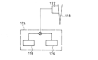
図3には本発明の一実施形態にかかる原子間力顕微鏡の概略構成が示されている。なお、前記従来技術と対応する部分には符号100を加えて示し説明を省略する。
同図に示す原子間力顕微鏡120は、針状プローブ118と、加振手段122と、検出手段124を含む。
【0021】
ここで、前記針状プローブ118は、例えば可撓性を有するファイバプローブを用いることができる。
また、前記加振手段122は、例えばモータ126と、回転体128を含み、この加振手段122は、回転体128の下面に、プローブ118の試料側先端部118aとは反対側先端部118bを、モータ126の回転軸O上を外し、設けている。
【0022】
また、この加振手段122は、プローブ試料側先端部118aが、測定試料表面112とプローブ118の間に働く原子間力の増減に応じた径を持つ真円、楕円等の円を描くように、該先端部118aを撓らせながらプローブ118を回転させる。
さらに、この加振手段122は、測定試料表面112とプローブ118の間の距離が近接ないし離隔する方向、つまり図中上下方向にもプローブ118を振動させる。つまり、タッピングする。
【0023】
前記検出手段124は、例えばプローブ照射部130と、光検出部132と、信号処理部134を含む。
ここで、前記プローブ照射部130は、例えばレーザダイオード(LD)等よりなり、プローブ118の先端部118a近傍にプローブ光L1を照射する。
また、前記光検出部132は、プローブ118aからの反射ないし透過プローブ光L2を検出する。
【0024】
前記信号処理部134は、光検出部124で得た反射ないし透過プローブ光L2から、プローブ試料側先端部118aが描く回転円の半径r等の径の増減情報を得る。この回転半径rの増減から測定試料表面112とプローブ118の間の距離を求める。これをパーソナルコンピュータ136に供給する。
【0025】
つまり、本実施形態では、加振手段122により、測定試料表面112とプローブ118の間の距離が近接ないし離隔する方向、図中上下方向にプローブ118を振動させ、測定試料表面112とプローブ118の間に働く原子間力の増減に応じた径を持つ円を描くように、試料側先端部118aを撓らせながらプローブ118を回転させる。
【0026】
そして、本実施形態では、加振手段122により、測定試料表面112とプローブ118の間の距離を近接させ、検出手段124により、両者間に働く原子間力によるプローブ先端部118aが描く回転半径の増減を検出し、該回転半径の増減から、該測定試料表面112とプローブ118の間の距離情報を得る。
なお、本実施形態では、測定試料表面112を走査するため、XYZの3軸ステージ138と、ステージ移動手段140と、ステージ制御手段としてのパーソナルコンピュータ136を含む。
【0027】
ここで、ステージ移動手段140は、測定試料112が置かれた3軸ステージ138をXYZ方向に移動可能である。
また、パーソナルコンピュータ136は、検出手段124からの測定試料表面112とプローブ試料側先端部118aの間の距離情報が一定となるように、ステージ移動手段140を介して3軸ステージ138の動作を制御する。
【0028】
そして、3軸ステージ138を駆動し測定試料表面112を走査しながら、ステージ移動手段140に加えた電圧のZ成分、つまり図中上下方向の成分等をコンピュータ136により画像化し、測定試料表面112の凹凸画像を得る。これをモニタ142に表示する。
また、本実施形態では、パーソナルコンピュータ136の入力デバイス144を用いて各種の設定が可能である。
【0029】
例えば、プローブ共振周波数などの設定が可能であり、パーソナルコンピュータ136は、入力デバイス144からのプローブ共振周波数で加振手段122の動作を駆動回路146を介して制御する。
本実施形態にかかる原子間力顕微鏡120は、概略以上のように構成され、以下にその作用について説明する。
すなわち、3軸ステージ等により、プローブ118と測定試料表面112との距離を、例えば1nm程度までに近づけると、両者の間には原子間力(引力又は斥力)が働く。
【0030】
この原子間力(引力又は斥力)を検出手段により検出し、3軸ステージによりこれが一定となるように試料表面を走査する。
このために、測定試料表面112を三次元駆動できる3軸ステージ138に載せ、原子間力を一定に保つように測定試料表面112を走査すれば、両者の距離は一定に保たれ、プローブ118は、測定試料表面112の凹凸を原子の尺度でなぞることになる。
【0031】
このとき、コンピュータ136により、ステージ移動手段140に加えた電圧の縦方向成分の変化を画像化すれば、これが測定試料表面112の形状に対応することになる。
ここで、測定試料表面112とプローブ118の間の距離を制御するため、プローブを測定試料表面の一軸方向に振動させるシアフォースフィードバック法が一般的に用いられる。
しかしながら、このシアフォースを用いると、測定試料表面とプローブの間に働く原子間力の横ずれ成分を検出することとなるので、一般的なカンチレバープローブを用いて原子間力の縦方向成分を検出した場合に比較し、感度が一桁以上低下してしまう。
【0032】
例えば、測定試料表面112の走査方向によっては、同一の測定試料表面であるにもかかわらず、得られた測定試料表面の凹凸画像には、差が生じるおそれがある。
そこで、本実施形態においては、前記シアフォースに代えて、以下に示す手法を用いることとしている。
【0033】
その作用について図4〜図6を参照しつつ説明する。
なお、図4は、プローブ118の回転状態を示す斜視図、図5は同様の正面図、図6は同様の上面図である。
すなわち、本実施形態にかかる顕微鏡120では、図4に示すように、プローブ試料側先端部118aが、測定試料表面112とプローブ試料側先端部118の間に働く原子間力の増減に応じた半径rを持つ円を描くように、該先端部118aを撓らせながらプローブ118を回転可能させている。
【0034】
そして、図5(a)に示すように、測定試料表面(図示省略)とプローブ118の間の距離が十分に離れた状態から、つまり両者の間に原子間力が働かない距離から、プローブ118を図中上下方向にも振動させながら、測定試料表面とプローブ試料側先端部118の間の距離を近接させる。
すなわち、ステージを図中上方向に駆動し、測定試料表面とプローブ118の間の距離を近接させる。
【0035】
このとき、測定試料とプローブ118間の距離は十分離れており、両者の間には原子間力が働いていないので、プローブ先端部118aは、遠心力F0のみの影響を受け、半径rの回転円を描く。
そして、測定試料表面112とプローブ118間の距離が近接すると、両者の間には原子間力が働く。この原子間力の増減に応じて、プローブ試料側先端部118aが描く回転円の半径rが変わる。
【0036】
例えば、同図(b)に示すように、図中、測定点P0からの原子間力(斥力F1)がプローブ試料側先端部118aに働くと、先端部118aには、力成分F2と力成分F3が働くので、先端部118aは、図中外側に引っ張られ、回転円径は、原子間力(斥力F1)に応じた分Δrだけ半径が増加する。
つまり、原子間力が働いていないときの回転円径をrとすると、この場合の回転半径は、r+Δrとなる。
【0037】
一方、同図(c)に示すように、図中、測定点P0からの原子間力(引力F4)がプローブ先端部118aに働くと、先端部118aには、力成分F5と力成分F6が働くので、先端部118aは、内側に引っ張られ、回転円径は、原子間力(引力F4)に応じた分Δrだけ半径が減少する。
つまり、原子間力が働いていないときの回転半径をrとすると、この場合の回転円径は、r−Δrとなる。
【0038】
このように、本実施形態では、同図(a)〜(c)に示したように、原子間力の縦方向の成分、つまり図中、上下方向の原子間力の変化を、回転半径rの増減として検出している。
このような原子間力に応じた回転半径rの増減を、図6に示すように、例えば測定点P0の周囲に配置されたプローブ照射部114、光検出部116により検出する。この回転半径rの増減情報から、後段の信号処理部やコンピュータ136により、測定試料表面112とプローブ118の間の距離を求めている。
【0039】
この結果、本実施形態にかかる原子間力顕微鏡120によれば、測定試料表面112とプローブ118の間の距離の測定に、測定試料表面112とプローブ118間に働く原子間力の縦方向成分を、回転半径rの増減として検出しているので、横ずれ成分、つまりシアフォースを用いた場合に比較し、検出感度の向上が図られる。
【0040】
また、従来のようにプローブを、測定試料表面で一軸方向に振動させると、検出手段の数と配置には制限があったのに対し、本実施形態にかかるプローブ顕微鏡によれば、測定試料表面112とプローブ118間に働く原子間力の縦方向成分を、回転半径rの増減として検出しているので、前記検出手段の配置と数には制限がなくなる。
【0041】
したがって、本実施形態においては、検出手段、特に検出部116を例えば図6に示す測定点P0の周囲の任意の位置に、所望の数だけ配置することができるので、従来極めて困難であった、検出部116の配置の自由度の向上が図られ、また検出部116の数を増加すれば、検出感度の向上が図られる。
【0042】
また、本実施形態にかかる顕微鏡120によれば、試料とプローブ間に働く原子間力の増減に応じた径を持つ円を描くように、先端部118aを撓らせながらプローブ118を回転可能プローブを回転させるので、シアフォース等を用いた場合には非常に困難であった、測定試料表面112の走査方向によらず、等方的な測定を良好に行うことができる。
【0043】
なお、本発明のプローブ顕微鏡は、前記構成に限定されるものではなく、発明の要旨の範囲内で種種の変形が可能である。
例えば、本実施形態にかかる顕微鏡では、一般的な測定系に用いられる各種の機構に代えて、以下に示す種種の機構を付加することが好ましい。
【0044】
SFディテクタ
例えば、プローブ118からの透過ないし反射プローブ光L2は、一般にレンズ付き、あるいはレンズ無しのPINフォトダイオード等で検出する。このレンズには、球面、あるいは非球面レンズが用いられる。
しかしながら、レンズを用いると、検出手段の感度を上げることができる横方向の光に加えて、縦方向の光も集光してしまう。
【0045】
このため、プローブの振幅、あるいは回転半径の検出感度を低下させてしまうので、この点は、改善の余地が残されていた。
そこで、本実施形態にかかる顕微鏡では、例えば図7に示すSFディテクタ148を設けることが好ましい。
同図に示すSFディテクタ148は、プローブ118からの透過ないし反射プローブ光L2を、2分割以上の分割型のフォトダイオードなどの位置センサ150a,150bにより検出し、2つの光量の差分を検出し、この差分からプローブ118の回転半径rの増減を検出している。
【0046】
この結果、本実施形態にかかる顕微鏡によれば、同図に示すSFディテクタ148を用いると、プローブ先端118aからの透過ないしプローブ光L2を、差分検出することができるので、感度の大幅な向上を図ることが可能となる。
また、本実施形態においては、同図に示すSFディテクタ148を用いると、横方向からの光のみを集めることができるので、プローブ118の回転半径rの増減の検出感度を上げることも可能となる。
【0047】
SF信号回路
例えばプローブを測定試料表面で一軸方向に振動させる一般的なシアフォース法では、通常は、プローブの運動を検出する検出手段の信号を、プローブを運動させる信号の周波数にロックインして、該検出手段の信号をDC化していた。
しかしながら、前記ロックインには時間がかかり、プローブ顕微鏡では高速検出のための障害になっていた。また、ロックインを的確に行うための位相の調整が必要であり、測定のための手間がかかるので、この点は、改善の余地が残されていた。
【0048】
そこで、本実施形態にかかる顕微鏡では、図7に示すSF信号回路152を設けることも好ましい。
同図に示すSF信号回路152は、例えば前記SFディテクタ148で得た信号の振幅強度をDCに変換する。
このSF信号回路152としては、例えば、実効値に変換する絶対値回路、及びRMS/DCコンバータなどよりなる群から選ばれた一の回路が用いられる。
【0049】
この結果、本実施形態にかかる顕微鏡によれば、同図に示すSF信号回路152を設けると、一般的なロックインを行った場合に比較し、小規模でSFディテクタ148で得た信号のDC化を行うことが可能となる。
しかも、測定のための位相等の調整が必要がないので、測定系全体の高速化を図ることが可能となる。
【0050】
フィードバック回路
例えば、プローブ顕微鏡、特に原子間力顕微鏡の場合には、走査のためのフィードバック回路は、原子間力の変化に対し原子間力が大きい場合も、小さい場合も一様に応答する。
このため、原子間力が小さい場合は不必要な高精度に、また精度のいらない原子間力が小さい場合は低精度に、また原子間力が大きい場合は精度が不足するという欠点があり、この点は、改善の余地が残されていた。
【0051】
そこで、本実施形態にかかる顕微鏡では、前記図7に示すフィードバック回路154を設けることも好ましい。
すなわち、同図に示すフィードバック回路154は、原子間力の変化に対し対数的に、あるいは指数関数的に応答するようにしている。
この結果、本実施形態にかかる顕微鏡は、同図に示すフィードバック回路154を設けると、原子間力の変化に対し対数的に、あるいは指数関数的に応答するので、原子間力が小さい場合は、間引いて、また原子間力が大きい場合は、密度を高くフィードバックすることが可能となる。
【0052】
つまり、本実施形態にかかる顕微鏡は、同図に示すフィードバック回路154を設けると、精度のいらない原子間力が小さい場合は低精度に、また、より精度の必要な原子間力が大きい場合は高精度に、それぞれ適切なフィードバックを行うことが可能となるので、効率的に測定精度を上げることが可能となる。
また、本実施形態にかかる顕微鏡は、同図に示すフィードバック回路154を用いると、原子間力が大きい場合には、フィードバックの密度が高くなるため、フィードバックの高速化と高安定化を図ることも可能となる。
【0053】
SF調整用表示機構
例えば、プローブ顕微鏡では、プローブ変位を検出するための検出器、あるいは光源の調整等の際は、通常は、プローブと試料との距離の制御に用いられる信号をモニタしながら、それが最適になるように調整されるか、目視で光が検出器に入っていることを確認しながら調整する。
【0054】
しかしながら、プローブと試料の距離の制御に用いられる信号には、プローブ変位検出のための検出器、光源、プローブの位置関係の他にも、プローブと試料の距離などの様々な信号成分が含まれる。
このため、前記調整を直感的に行うことができず、調整手順は複雑で困難なものになっており、改善が強く望まれていた。
そこで、本実施形態では、複数の光検出器の信号又は分割検出器自体の信号を別個に表示可能な、例えば前記図7に示すようなモニタ142と、その表示を元に、前記調整が可能なパーソナルコンピュータ136などを設けている。
【0055】
この結果、本実施形態にかかる顕微鏡では、同図に示すモニタ142やコンピュータ136等を設け、複数の光検出器等の信号を別個にモニタ142に表示し、そのモニタの表示を元にコンピュータ136により前記調整を行うことにより、検出器とプローブ光L1の位置関係を、モニタ142で直接目視することができるので、従来極めて困難であった前記調整が容易となる。
【0056】
加振手段、検出手段
また、前記構成では、回転半径rの増減を検出するため、プローブ118からの反射ないし透過プローブ光L2の強度変化を用いた例について説明したが、本発明の顕微鏡は、これに限定されるものではなく、これに代えて、例えば石英振動子、及び圧電素子(PZT)よりなる群から選ばれた一の部品を用いることができる。
【0057】
また、前記構成では、加振手段としてモータを用いた例について説明したが、本発明の顕微鏡は、これに限定されるものではなく、これに代えて、例えば圧電素子などを用いることもできる。
ここで、本実施形態にかかる顕微鏡では、圧電素子としては、図8に示すように、プローブの後端側118bのほぼ全周囲に亘って、加振手段としての対向配置の加振電極対156a,156bと、検出手段としての対向配置の検出電極対158a,158bが交互に配置された、例えば4分割以上等の分割型円筒状圧電素子160を用いることが好ましい。
【0058】
この場合には、例えば制御手段としてのパーソナルコンピュータ136等により、加振電極対156a,156bによるプローブ118の加振と、検出電極対158a,158bによる回転半径rの増減の検出を、同時又は時分割に交互に行わせることも好適である。
これにより、加振手段と検出手段を別個独立に設けた場合に比較し、省スペース化が図られるので、装置の小型化が図られる。
【0059】
SF光学系
プローブ顕微鏡の光学系では、回転半径rの増減を検出するため、レーザ光等のプローブ光L1を、遠方からプローブに集光、照射し、反射プローブ光を遠方の検出部で捉えることにより、プローブ118の周りの少なくとも2方向にスペースを必要とする。また、プローブ118を交換する毎に、プローブ光と検出部の両方の位置を再調整する必要があった。
【0060】
また、プローブ光を照射するプローブ先端部にプローブ光が届くようにするため、プローブ先端部付近には、障害物がないようにする必要があるため、水中測定などの使用を特殊な条件下での測定の妨げとなっており、これらの点は、各種の測定を必要とするプローブ顕微鏡では改善の余地があった。
そこで、本実施形態にかかる本実施形態にかかるプローブ顕微鏡は、図9に示すSF光学系159を設けることも好ましい。
【0061】
同図に示すSF光学系159は、プローブ照射部114と、光ファイバ162,164,166と、1:1ファイバ分岐のファイバカプラ168と、光検出部116と、レンズ170,172を含み、光ファイバ164で、プローブ118の振動数・振幅を干渉検出する。
すなわち、同図に示すSF光学系159は、プローブ118からの反射プローブ光L2と、ファイバカプラ168により分岐した一方のファイバ164の端面での反射光L3の干渉光L4の波長を光検出部116で検出し、プローブ118の回転半径rの増減を検出する。
【0062】
この結果、本実施形態にかかるプローブ顕微鏡によれば、同図に示すSF光学系159を用いると、プローブ118の回転半径rの増減を検出する際は、プローブ先端部118aの極近傍に、光ファイバ164の端面を配置すればよく、遠方から光学的に覗く必要はない。
また、本実施形態にかかるプローブ顕微鏡によれば、同図に示すSF光学系159を用いると、プローブ交換時の調整は、光ファイバ164の端面の一箇所を調整するだけでよい。
【0063】
また、本実施形態にかかるプローブ顕微鏡によれば、同図に示すSF光学系159を用いると、光ファイバ164の端面とプローブ118を任意の雰囲気下に置けばよいので、測定環境も選ばない。
【0064】
プローブ加振周波数設定の自動化機構
プローブの共振周波数の設定は、共振周波数を何らかの方法で測定した後、別手段によってプローブ加振周波数を設定する手法が一般的に用いられる。
しかしながら、この場合には、使用者は、少なくとも2回操作を行う必要があり、手順が煩雑であったため、この点は改善の余地が残されていた。
そこで、本実施形態にかかるプローブ顕微鏡では、図10に示すプローブ加振周波数設定機構174を設け、設定の自動化を行うことが好ましい。
【0065】
すなわち、同図に示すプローブ加振周波数設定機構174は、ホワイトノイズ発生器176と、正弦波発生器178を含む。
そして、これらの発生器176,178からの信号を圧電素子(PZT)等の加振手段122に供給している。
【0066】
すなわち、同図に示すプローブ加振周波数設定機構174では、プローブの加振信号をホワイトノイズ発生器176からのホワイトノイズに切り替えて、共振周波数を設定した後、或いは加振信号に正弦波発生器178からの順次異なる周波数を加えて、強度を測定による共振周波数測定した後、算出された共振周波数に設定している。
【0067】
この結果、本実施形態にかかるプローブ顕微鏡によれば、同図に示すプローブ加振周波数設定機構174を用いると、1回の操作で共振周波数の測定と、設定を行うことが可能となるので、操作容易化の向上を図ることが可能となる。
【0068】
ステージ
例えば、プローブ顕微鏡では、プローブの位置を動かすことができないので、プローブを走査せずにプローブ位置を固定し、ステージを走査することにより、測定試料の表面を走査する手法が用いられる。
このため、前記プローブ顕微鏡の一般的な試料ステージとしては、例えば図11に示すように、円筒状等の圧電素子(PZT)180を下から立ち上げ、該圧電素子180の上に、測定試料112のステージ138を設けたものがある。
【0069】
しかしながら、このようなステージを用いると、ヘッド全体の大きさが大きくなり、温度安定性が悪い。
また、この試料ステージとしては、図12に示すように、前記圧電素子180を上からぶら下げる手法も考えられる。
しかしながら、この場合には、圧電素子180に引っ張り応力が働くことにより、圧電素子180と、この圧電素子180の各支持部材182,184の接合面、あるいは圧電素子180自体の破壊を招くおそれがあり、この点は改善の余地が残されていた。
【0070】
そこで、本実施形態にかかるプローブ顕微鏡では、前記一般的なステージを用いることは一応可能であるが、これに代えて、例えば図13〜図14に示す試料ステージを用いることも好ましい。
なお、図13(a)はステージの縦断面図、同図(b)は上面図である。
すなわち、同図に示す試料ステージ186では、駆動機構としての円筒型圧電素子188を間に挟んで上側支持部材190と下側支持部材192を設け、円筒型圧電素子188をはじめ、これらの各支持部材190,192の中空部にプローブ118を通している。
【0071】
そして、支持部材192の上に試料台194を設け、各支持部材190,192により、圧電素子188に常に圧縮応力がかかるようにしている。
この結果、本実施形態にかかる顕微鏡では、同図に示す試料ステージ186を用いると、駆動機構としての円筒状圧電素子188の空洞部分(中空部分)をプローブのための空間として有効的に利用することができるので、ヘッド全体をコンパクト化することが可能となる。これにより、温度安定性の向上が図られる。
【0072】
また、本実施形態においては、同図に示す試料ステージ186を用いると、圧電素子188には常に圧縮応力が働くので、圧電素子188と各支持部材190,192の接合面、又は圧電素子188自体の破壊を防ぐことが可能となる。
さらに、本実施形態においては、前記各構成部材を、同様な構造を同芯円上に配置することにより、移動距離の大きい多軸操作が可能となる。
【0073】
なお、前記圧電素子188としては、任意のものを用いることができるが、例えば上下方向と、水平面方向の2軸駆動を実現する5分割円筒状圧電素子、及び上下方向の駆動を実現する積層型の円筒状圧電素子(ドーナツ型)と、水平方向の2軸駆動を実現する4分割圧電素子よりなる群から選ばれた一の圧電素子を用いることも可能である。
【0074】
試料ステージの構造
微動用の3軸ステージやプローブ位置の駆動機構として、通常は、前記5分割円筒型圧電素子、3本の積層型圧電素子を直交して組み合わせたもの、4分割円筒状圧電素子(X,Y)と、該圧電素子とは異なる位置に3つの積層型圧電素子を垂直に並べてZ軸駆動機構したもの等が用いられる。
【0075】
このうち、5分割円筒型円筒状圧電素子は、Z軸の駆動量を稼ぐために縦方向に長くする必要があり、温度変化により容易にドリフトが発生する。
また、移動量を稼ぐために、肉厚をできるだけ薄くする必要があり、共振周波数が著しく低下し、高速な位置移動ができない。
また、前記3本の積層型圧電素子を直交したものでは、組み合わせの形状が非対称であり、非対称なドリフトが発生する。
【0076】
また、前記4分割円筒状圧電素子(X,Y)と、圧電素子とは異なる位置に3つの積層型圧電素子を垂直に並べてZ軸駆動機構としたものでは、配置に多大なスペースを必要とする。
また、Z軸として働く3つの積層型圧電素子の移動量が全て等しいとは限らないので、移動に伴い傾きが発生する危険があり、また、圧電素子の破壊を招く可能性もあり、これらの点は、改善の余地が残されていた。
そこで、本実施形態にかかる顕微鏡では、図14に示す駆動機構196を用いることも好ましい。
【0077】
同図に示す駆動機構196は、上下方向に駆動する穴あき型積層ピエゾ198と、平面方向2軸に駆動する4分割円筒状圧電素子200,202を上下方向に近接して一体化している。
この結果、本実施形態においては、同図に示す駆動機構196を用いると、駆動機構全体の全長をより短くしても、同じ駆動範囲を確保することができるので、例えば5分割円筒状圧電素子を用いた場合に比較し、圧電素子の温度変化に起因する熱ドリフトを大幅に低減することが可能となる。
【0078】
また、本実施形態においては、同図に示す駆動機構196を用いると、5分割円筒状圧電素子を用いた場合に比較し、上下駆動部分の肉厚が非常に大きくなるので、圧電素子全体の共振周波数が格段に増加し、より高速に試料ステージを駆動することが可能となる。
【0079】
また、本実施形態においては、同図に示す駆動機構196を用いると、同心円状の構造となるため、積層型圧電素子を3方向組み合わせた構造に比較し、水平面方向の機械ドリフトが格段に低減することが可能となる。
なお、本実施形態において、同図に示す駆動機構196は、試料ステージの駆動機構などに限られるものではなく、プローブ位置の駆動にも用いることが可能である。
【0080】
試料交換機構
測定試料を交換する方法としては、従来より種種の方法が用いられ、例えば顕微鏡の側方からV溝に沿って試料ステージを挿入するなどの方法が一般的に用いられる。
しかしながら、この場合には、構造が対称性を欠いているので、不慮の方向にドリフトしてしまう。
また、この場合には、試料ステージの面が決まっているので、試料の厚みによって試料表面の絶対位置が変わってしまう。
【0081】
また、試料ステージの面が決まっているので、測定可能な試料の厚みに制限があり、これらの点は、ステージを駆動することにより試料表面を走査する原子間力顕微鏡や近接場光学顕微鏡などのプローブ顕微鏡では改善の余地があった。
そこで、本実施形態にかかるプローブ顕微鏡では、図15に示す試料ステージ204を用いることも好ましい。
【0082】
すなわち、同図に示す試料交換機構204は、支持部材206,208の両者に直接、ねじ溝210,212を切ってあり、両者を螺合可能にしている。
また、同図に示す試料交換機構204は、支持部材206,208が十分に肉厚に作られている。このため、支持部材のねじ込む量を調節することにより、ステージの高さを調整することが可能である。
【0083】
例えば同図(a)に示す状態の支持部材206に、さらに支持部材208をねじ込むと、同図(b)に示すようにプローブ118と測定試料112間の距離を近接させることができる。
また、同図に示す試料交換機構204は、支持部材206の下方に貫通穴が設けられている。
このため、同図に示す試料交換機構204は、支持部材206の下方の貫通穴から光学的試料観察、光照射、集光などを行うことが可能である。
【0084】
この結果、本実施形態にかかる顕微鏡によれば、同図に示す試料交換機構204を用いると、各構成部材の構造が同心円状であるので、水平方向のドリフトが少なくなる。
また、本実施形態にかかる顕微鏡によれば、同図に示す試料交換機構204を用いると、支持部材208の支持部材206へのねじ込む量を調整することにより、測定試料112の厚みに合わせて、ステージの高さを変化させることができるので、より広範囲の厚みの測定試料を測定することが可能となる。
【0085】
なお、前記構成に加えて、図16に示すように直接試料112を載せる試料台214を、さらに中間に設け、該試料台214を固定すれば、支持部材208の回転にかかわらず、該試料台214が回転しないようにすることも可能となる。
【0086】
プローブ交換機構
例えば、近接場光学顕微鏡などのプローブ顕微鏡では、プローブの交換の際は、光ファイバを部材と部材の間を通すための光ファイバのプローブと反対の端を通す必要があった。
しかしながら、この場合には、光ファイバがからまったり、切れたりすることがあり、取り扱いが面倒であった。
【0087】
また、この場合には、プローブの位置の周りにはステージや柱があり、スペースが少なく、交換し難い構造であった。
また、プローブ交換のためにプローブ部分の位置を変える構造をつけた場合は、全体の共振周波数が低下し、ドリフトや振動の影響を受けやすく、これらの点は改善の余地が残されていた。
【0088】
そこで、本実施形態にかかるプローブ顕微鏡、特に近接場光学顕微鏡では、図17に示すプローブ交換機構215を用いることが好ましい。なお、同図(a)は下面図、同図(b)は同様の縦断面図である。
すなわち、同図(a)に示すように、試料ステージ216の中心部には、十分大きな貫通穴217があいている。
【0089】
そして、プローブ交換の際は、同図(b)に示すようなプローブ固定部220が貫通穴217よりステージ216をくぐり抜けて、該ステージ216の下面から突出した状態でプローブ118を交換することとしている。
また、本実施形態では、同図に示すプローブ交換機構を用いると、ステージ部分216と、プローブ固定部220には、それぞれスリワリ224,222が入っており、プローブ118の交換時には、該スリワリ222,224を用いてファイバ118を貫通穴217に通すことも可能である。
【0090】
この結果、本実施形態にかかる顕微鏡では、同図に示すプローブ交換機構215を用いると、プローブの交換時、プローブ118の周りには、障害物がなくなるので、交換が容易となる。
また、本実施形態にかかる顕微鏡では、同図に示すプローブ交換機構215を用いると、交換のための不要な構造を設ける必要がないので、構造を頑強にすることが可能となり、ドリフトや振動の影響を受け難くなる。
【0091】
また、本実施形態にかかる顕微鏡では、同図に示すプローブ交換機構215を用いると、前記スリワリ222,224を介すことにより光ファイバを絡ませることなく、容易にプローブ固定部220にプローブ118を取り付けることが可能となる。
【0092】
ステージ粗動機構(その1)
低温で動作する試料ステージの粗動機構には、圧電素子が一般的に用いられる。その駆動法としては、例えばインチワークやステージ面に直交して配置した円筒状の圧電素子に、鋸歯状の印加電圧を加える慣性駆動法などが知られている。
しかしながら、このような駆動法では、試料ステージは、ステップ状に動作するので、正確に位置合わせすることができない。
【0093】
また、実際の移動量は、ステージの摩擦に依存しているため、経時変化があり、前記粗動機構は、一般的な測定系の試料ステージの粗動機構としては十分に使用できるが、本実施形態にかかるプローブ顕微鏡のように微小試料等も扱う場合には、前記問題点は、改善する余地がある。
そこで、本実施形態にかかる顕微鏡では、粗動ステージとして、例えば図18に示す粗動ステージ225を用いることが好ましい。
【0094】
同図に示す粗動ステージ225は、ステージ226の一側面をバイモルフ228で押して駆動することとしている。
この結果、本実施形態にかかる顕微鏡では、同図に示す粗動ステージ225を用いると、バイモルフ228への印加電圧を変えることで、図中、破線で示されるように、バイモルフ228はステージ226側に沿ったり、図中、実線で示されるように元の状態に戻るので、ステージ226を、例えば図中左方向の任意の位置に、滑らかに位置決めすることが可能となる。
【0095】
また、本実施形態にかかる顕微鏡では、同図に示す粗動ステージ225を用いると、ステージ226の移動量は、バイモルフ228の特性にのみよるため、経時変化を大幅に低減することが可能となる。
【0096】
ステージ粗動機構(その2)
前述のように低温で動作する試料ステージの粗動機構には、一般的に圧電素子が用いられる。例えば、インチワークやステージ面に直交して配置した円筒状圧電素子に、鋸歯状の印加電圧を加えることによる慣性駆動法等が知られている。
これらの駆動法では、ステージ面に対して各部材を立体的に組み上げる必要があり、温度安定性が悪くなり、ドリフトが大きい。
【0097】
また、駆動方向が直線方向に限られ、回転運動することができず、このような粗動機構は、一般的な測定系の試料ステージの粗動機構としては十分に使用できるが、本実施形態にかかるプローブ顕微鏡のように、各種の駆動が必要となる場合には、前記粗動機構をそのまま用いると不便が生じる。
そこで、本実施形態にかかる顕微鏡では、図19(a)に示す粗動ステージ229を用いることも好ましい。
【0098】
同図に示す粗動ステージ229は、ステージ226の一側面に直接貼り付けられ、一端が自由端になっている圧電素子230が用いられる。
そして、このような圧電素子230に、任意波形の印加電圧をかけることにより、同図(b)に示すように、圧電素子230の一端が縮み、元に戻ることで、ステージ226に慣性力を与えてステージ226を、例えばx方向に動かすこととしている。
【0099】
なお、前記図19に示す粗動ステージ229では、ステージ226の一側面に1つの圧電素子230を設け、例えばステージ226をx方向に移動した例について説明したが、これに代えて、図20に示すように、圧電素子230a〜230dをステージ226の4側面に配置すれば、XとYの2軸とも、前後に動かすことが可能である。
また、図21に示すように、圧電素子230a〜230hを、ステージ226の各4辺に、2つづつ十分間隔を空けて配置すれば、前記XとYの2軸に加えて、回転も可能となる。
【0100】
この結果、本実施形態にかかる顕微鏡によれば、前記図19〜図21に示す粗動ステージを用いると、ステージ226の側面に、圧電素子230等の全ての部材を収めることができる。
このため、粗動機構も含めたステージを薄くできるので、縦(Z)方向の温度安定性を高めることができる。
【0101】
さらに、図21に示す粗動ステージを用いると、圧電素子230をステージ226の各4辺に、2つづつ十分間隔を空けて配置しているので、従来極めて困難であった回転運動も行うことができる。
【0102】
ステージダイナミックレンジの拡大
プローブ顕微鏡では、ステージの走査には、通常は、1つの圧電素子が駆動機構として用いられる。
そして、圧電素子のスキャン範囲を超えた場合は、別の2回の測定に分けて独立に行う必要がある。
このため、プローブ顕微鏡では、ステージの駆動機構としての圧電素子のスキャン範囲をできるだけ大きく設計する必要がある。
【0103】
しかしながら、現実的な圧電素子のスキャン範囲には限界がある。また、スキャン範囲を大きくすればするほど、ステージが巨大化し、また測定の安定性が悪くなる傾向にあり、これらの点は改善の余地が残されていた。
そこで、本実施形態にかかる顕微鏡は、図22に示す複合型3軸ステージ232を用いることも好ましい。
【0104】
同図に示す複合型3軸ステージ232は、微動用の3軸ステージ234と、粗動用の3軸ステージ236を含む。
ここで、前記微動用の3軸ステージ234は、駆動機構として、例えば圧電素子などが用いられ、その上に試料112が置かれた状態で、例えば図22中、XYZの3軸方向に微小移動する。
【0105】
また、前記粗動用の3軸ステージ236は、駆動機構として、例えばステッピングモータ等が用いられ、プローブ118をつるした状態で、例えば同図中、XYZの3軸方向に、前記微動用の3軸ステージ234に比較し高速に移動可能である。
【0106】
そして、微動用の3軸ステージ234をスキャン中、必要なスキャン範囲を超えた際は、粗動用の3軸ステージ236を必要量駆動する。その後に、再度、微動用の3軸ステージ234を駆動し、データを結合すれば、ステージの移動量は、十二分に確保することが可能となるので、圧電素子等の微動用の3軸ステージ234のスキャン範囲を超えた測定も、前記問題を生じることなく行うことが可能となる。したがって、装置をコンパクト、かつ、高安定に組むことも可能となる。
【0107】
測定中のZ退避機構
従来のプローブ顕微鏡では、温度ドリフト、試料位置のずれ、極端な試料傾きや凹凸等によって、マッピング測定中にプローブと試料が衝突し、プローブ又は試料が損なわれるおそれがあり、この点は、改善する余地があった。
そこで、本実施形態にかかる顕微鏡では、前記図22に示すように、測定中に、パーソナルコンピュータ136がZ軸のスキャン範囲のある値を超えてプローブ118と試料112が接近したと判断した場合には、該パーソナルコンピュータ136が、測定を中止して、粗動用の3軸ステージ236を駆動して、プローブと試料112の間の距離を離すようにしている。
【0108】
つまり図中、Z軸方向である上方にプローブ118を移動している。
この結果、本実施形態にかかる顕微鏡では、このような測定中のZ退避機構を用いると、温度ドリフト、試料位置のずれ、極端な試料傾きや凹凸等によって、マッピング測定中にプローブと試料が衝突し、プローブ又は試料が損なわれることを防ぐことが可能となる。
【0109】
自動接近機構
例えば、原子間力顕微鏡などの場合、プローブと試料との間の距離を十分に離した位置から、原子間力信号に変化が現れるまで順次読み取りながら、プローブと試料との間の距離を変化させるのが一般的であった。
この場合、プローブと試料が十分に離れている場所でも、信号の読み取りを行うため、不要な時間がかかり、この点に関しては、改善の余地が残されていた。
【0110】
そこで、本実施形態にかかる顕微鏡では、前記図22に示すような試料112とプローブ118間の距離を、圧電素子などの微動用の3軸ステージ234を用いて近づけ、原子間力信号を読み取り、フィードバックがかからなかった場合は、微動用の3軸ステージ234を用いて再度近づけ、読み取りを繰り返す。
これをフィードバックがかかるまで繰り返し、フィードバックがかかったら停止することとしている。
【0111】
また、前記接近に先立って、側面上方からプローブ118と測定試料112との関係を観察するCCDカメラ237等からの画像をモニタ142で見ながら、手動にてプローブ118と測定試料112との距離をモニタ142の解像度程度まで接近させることも可能である。
この結果、本実施形態にかかる顕微鏡によれば、プローブ118と測定試料112との距離が明らかに離れている部分は、粗動用の3軸ステージ236を用いて高速に移動し、必要最小限の部分だけ信号を読み取りながら、粗動用の3軸ステージ234を移動するので、前記接近にかかる時間を格段に短縮化することが可能となる。
【0112】
近接場光学顕微鏡
また、前記構成では、試料とプローブ間の相互作用に、原子間力を用いた原子間力顕微鏡を想定し、試料表面の形状等を把握する例について説明したが、本発明のプローブ顕微鏡は、これに限定されるものではなく、試料とプローブ間の相互作用に光近接場を用いた近接場光学顕微鏡でもよい。
また、本発明のプローブ顕微鏡は、試料の表面形状を把握するものに限定されるものではなく、プローブ位置における試料の成分等の分析をすることも可能である。
【0113】
その際は、例えば以下に示す近接場光学顕微鏡を用いることも好ましい。
図23には本発明の一実施形態にかかる近接場光学顕微鏡の概略構成が示されている。
同図に示す近接場光学顕微鏡238は、単色光源240からのレーザ光L6をレンズ242で平行光束とし、ビームスプリッタ244、収束レンズ246を介してプローブ118内に導入する。
【0114】
そして、光近接場をプローブ118の先端部118aから測定試料112に照射する。測定試料112からの反射光、散乱光、発光、蛍光、ラマン光等の光L7を、同一のプローブ118の先端部118aから集光し、レンズ246、ビームスプリッタ244、さらにはレンズ248を介して検出器250に導入している。
つまり、本実施形態では、プローブ118から励起光としてのレーザ光L6を照射し、同一のプローブ118で試料112からの光L7を集光している。
【0115】
ここで、従来の近接場光学装置を用いて振動分光学的ラマン分光や赤外分光を行う際には、プローブから光を照射し、外部のレンズや鏡で、反射光、散乱光、発光、蛍光、ラマン光を集光するイルミネーションモードがある。
また、外部から照射された光による反射光、散乱光、発光、蛍光、ラマン光をプローブで集光するコレクションモードもある。
しかしながら、これらのモードでは、試料ステージ付近に集光のための対物レンズを組み込んだり、レーザを導入するための光学系を別途、組み込む必要があり、装置が煩雑になる。
【0116】
また、反射測定の場合には、プローブが集光のために、或いはレーザ導入のために影になってしまうので、集光又は照射効率が悪く、また、試料ステージとプローブと干渉しないようにするため、対物レンズの倍率を大きくとることができない。
また、イルミネーションモードの場合は、フォトンの吸収機構によっては、照射された部分より広い面積から発光してしまい、空間分解能を著しく損なう場合がある。
【0117】
そこで、本実施形態にかかる近接場光学顕微鏡238は、前記問題を解決するため、同図に示すように、プローブ先端部118aより、光源240からの光L6を照射し、試料112からの光L7を、同一のプローブ118で集光している。
この結果、本実施形態にかかる顕微鏡238によれば、散乱近接場光の照射と集光を1つのプローブ118で実現することができるので、集光系の配置が非常に容易となる。
また、本実施形態にかかるプローブ顕微鏡238によれば、集光を行うプローブ118を試料表面112に対し非常に接近させることができるので、試料112からの散乱近接場光の集光に、まるで非常に高倍率のレンズを用いたかのように、高効率で集光することができる。
【0118】
なお、同図に示す顕微鏡238による、前記イルミネーション−コレクションモードを、プローブ118から励起光を照射し、同じプローブ118でラマン光を集光する近接場ラマン分光装置に用いることも可能である。
また、前記イルミネーション−コレクションモードを、プローブ118から赤外光を照射し、同じプローブ118で赤外光を集光する近接場赤外分光装置に用いることも可能である。
【0119】
また、前記イルミネーション−コレクションモードを、プローブ118から励起光を試料112に照射し、同じプローブ118で励起光により励起された測定試料112のラマン散乱光を集光する近接場ラマン分光装置に用いることも可能である。
さらに、前記イルミネーション−コレクションモードを、プローブ118から赤外光を試料112に照射し、同じプローブ118で測定試料112からの反射光を集光する近接場赤外分光装置に用いることも可能である。
【0120】
ビームスプリッタ
ところで、前記図23に示した近接場光学顕微鏡238において、ビームスプリッタ244として、1:1の比率で分ける一般的なビームスプリッタを用いると、プローブ118により集光された試料112からの光L7は、集光された量の半分しか取り出すことができず、高感度に試料の光を取り出す場合の妨げとなっていた。
【0121】
これは一般的な測定系に用いた場合には問題が生じないが、特に本実施形態にかかる近接場光学顕微鏡の光学系に用いた場合には、検出光としての近接場光は、一般的な検出光に比較し微弱な光であるため、他の測定系に明るさが必要であり、前記集光された量の半分しか取り出せないという問題は、深刻な問題であった。
そこで、本実施形態にかかる近接場光学顕微鏡238では、前記イルミネーション−コレクションモードを行うためのビームスプリッタ244として、1:1でない非対称ビームスプリッタ、ローパスフィルタ、バンドリジェクションフィルタ、バンドパスフィルタ、ファイバカプラよりなる群から選ばれた1つの光学部品を用いている。
【0122】
この結果、本実施形態にかかる近接場光学顕微鏡238によれば、前記1:1でない非対称ビームスプリッタを用いると、入射光を1:1の比率で分ける一般的なビームスプリッタを用いた場合に比較し、プローブから取り出した目的の光を50%以上の効率で取り出すことができるので、満足のゆく明るさが得られる。
【0123】
試料面観察機構
光ファイバを用いた近接場光学用プローブや、STMに用いられる金属プローブでは、配置上、真上からの顕微鏡観察が困難であった。また、凹面ミラー等を用いて観察することも考えられるが、その配置が制限されるので、見込み角を大きくとれない等の問題がある。これにより、十分な分解能が得られない場合がある。
【0124】
ここで、一般的な測定系では十分な分解能でも、より高分解能が求められる本実施形態にかかる顕微鏡で用いるには、見込み角を大きくとれず、高分解能化が困難な点は、改善の余地が残されていた。
そこで、本実施形態にかかる顕微鏡では、図24に示す試料面観察機構252を用いることが好ましい。
同図に示す試料面観察機構252は、プローブ118のホルダの根元、あるいはプローブアタッチメントの下部などのホルダ254に、ミラー256が取り付けられる。
【0125】
そして、そのミラー256を介して、さらにレンズ258,260を介して測定試料表面112の顕微鏡像L8を、CCD262等により観察することにより、測定試料表面112の真上からの観察を可能にしている。
この結果、本実施形態にかかる顕微鏡では、同図に示す試料面観察機構252を用いると、安価な構成で、従来極めて困難であった容易に真上から観察することが可能となる。
【0126】
また、本実施形態にかかる顕微鏡では、同図に示す試料面観察機構252を用いると、顕微鏡の対物レンズなどの配置が容易となり、見込み角をより大きくとれるので、満足のゆく高分解能を得ることも可能となる。
なお、前記ミラー256としては、穴あきミラー、スリワリミラー、穴あきプリズム、スリワリプリズム、アタッチメントを直接ミラー加工したミラー面などよりなる群から選ばれた一の光学部品を用いることが可能となる。
【0127】
また、前記ミラー256を介して顕微分光、あるいはマクロ分光を行うことにより、マクロ分光と顕微分光と近接場プローブ分光を行うことのできる原子間力顕微鏡を得ることが可能となる。
【0128】
ファイバ端面観察機構
例えば、近接場光学顕微鏡などのプローブ顕微鏡では、プローブにレーザ光を導入する調整は、プローブ先端部から射出されるレーザ光の強度を確認しつつ、位置調整を行うか、ファイバ端面からのレーザ反射光を観察しながら調整していた。
しかしながら、この場合には、ファイバのコアとレーザ光との位置関係を認識することができず、直感的に調整する必要があり、時間がかかるので、この点は、改善の余地が残されていた。
【0129】
そこで、本実施形態にかかる顕微鏡は、図25に示すファイバ端面観察機構264を用いることも好ましい。
同図に示すファイバ端面観察機構264は、例えばプローブ118から近接場光を測定試料に照射し、該プローブ、あるいは集光レンズなどにより、該測定試料からの散乱近接場光を集光する近接場光学顕微鏡などを想定している。
そして、このプローブ118につながる光ファイバのプローブ側とは反対側の光ファイバ端面265に、プローブ118に導入する単色光源266からのレーザ光L6をレンズ268、ビームスプリッタ270、レンズ272を介して照射している。
【0130】
このとき、同図に示すファイバ端面観察機構264は、光ファイバ端面265に白色光源274からの白色光L9を直接照射している。
この結果、本実施形態にかかる顕微鏡によれば、ファイバコア276とレーザ光の位置関係を、白色光源274からの光L9の照射により、レンズ272、ビームスプリッタ270、レンズ278及びCCD280により直接観察しながら、ファイバコア276とレーザ光L6の位置を調整することが可能となる。
【0131】
したがって、同図に示すファイバ端面観察機構264を用いると、調整すべき方向をその都度、確認することができるので、従来のように直感的に調整した場合に比較し、前記調整を迅速に、かつ、容易に行うことが可能となる。
【0132】
位置調整機構
光学素子やステージ等の部品の3軸方向、つまりXYZ方向の位置決めを行う際は、互いに直交する3軸方向に、各位置調整の軸が突出したものが一般的に用いられる。
しなしながら、前記調整のために互いに直交する3軸方向からアクセスするように組み込まれると、構成が複雑となる。また、3軸方向から調整する必要があり、作業が面倒であった。
【0133】
このため、比較的に簡略な測定系で用いるには問題とならない複雑な構成や操作であっても、一般的な測定系に比較し、より多機能を備えるために各種の操作が必要となる本実施形態にかかるプローブ顕微鏡では、構成の簡略化や操作容易化が必要となり、前記問題は改善の余地が残されていた。
そこで、本実施形態にかかる顕微鏡では、図26に示す位置調整機構281を用いることも好ましい。
【0134】
同図に示す位置調整機構281は、位置調整用ネジ282と、三角ブロック283と、を含む。
ここで、前記位置調整用ネジ282は、操作側の端部に取手284が設けられており、この取手284を回転させると、図中、i方向に移動する。
また、前記三角ブロック283は、取手側の斜面283aが位置調整用ネジ282の先端部282aと当接し、その対向面283bがステージ等の部品286に固定されている。
【0135】
この三角ブロック283は、位置調整用ネジ282が図中i方向に移動すると、その斜面283aの傾斜方向の図中j方向のみに移動可能となるように、その移動方向が、スライダ等(図示省略)により規制されている。
そして、XYZ3軸の位置を調整するには、同図に示す位置調整機構281を3つ設ける。
すなわち、X軸用三角ブロックがX方向のみに移動可能となるように、X軸用三角ブロックの斜面の向きと、X軸用スライダ等が規制するX軸用三角ブロックの移動可能な方向を考慮し、ステージ等の部品286のある面に、同図に示す位置調整機構281をX軸方向の位置調整用として設ける。
【0136】
また、Z軸用三角ブロックがZ方向のみに移動可能となるように、Z軸用三角ブロックの斜面の向きと、Z軸用スライダ等が規制するZ軸用三角ブロックの移動可能な方向を考慮し、ステージ等の部品286の、前記X軸用の位置調整機構が設けられた面と同一の面に、位置調整機構281をZ軸方向の位置調整用として設ける。
【0137】
また、Y軸用三角ブロックがY方向のみに移動可能となるように、Y軸用三角ブロックの斜面の向きと、Y軸用スライダ等が規制するY軸用三角ブロックの移動可能な方向を考慮し、前記ステージ等の部品286のX軸用の位置調整機構とZ軸用の位置調整機構が設けられた面と同一の面に、位置調整機構281をY軸方向の位置調整用として設ける。
【0138】
このように、同一の方向からXYZ3軸の位置調整が可能となるように、各位置調整用ネジの取手の方向を考慮している。
この結果、本実施形態にかかる顕微鏡では、前述のように同図に示す位置調整機構281を3つ、各軸方向の位置調整用に用いると、XYZ3軸の位置調整をする際は、使用者は同一の方向からアクセスすることが可能となるので、構成の簡略化と、操作容易化が図られる。
【0139】
なお、三角ブロック283の傾面283aの傾斜角度θを適当に決めることにより、位置調整用ネジ282の取手284の回転を拡大、又は縮小することが可能となる。
つまり、前記三角ブロック283の斜面283aの傾斜角度θを大きくすれば、前記位置調整用ネジ282の取手284の回転を拡大することが可能となる。一方、前記三角ブロック283の斜面283aの傾斜角度θを小さくすれば、前記位置調整用ねじ282の取手284の回転を縮小することができるので、位置調整機構281の設けられた部品286を適宜、かつ、容易に位置決めすることが可能となる。
【0140】
反射集光系
例えば、測定試料からの光を集光し、検出又は分光する測定系においては、一般に、単一の対物レンズを用いて集光していた。
この場合、光を集めることのできる見込み角は限られており、高感度測定の場合には光量が不足してしまう。
また、複数のレンズを用いることも考えられるが、これらの光を有効に結合する方法が知られず、効率的に感度を上げることができなかったため、前記光量不足の解決の手段としては採用するには至らなかった。
【0141】
そして、一般的な測定系では、特に問題とはならない光量の不足であっても、一般的な測定系に比較し、より微小な試料に関して、より高精度な測定が要求される原子間力顕微鏡や近接場光学顕微鏡などのプローブ顕微鏡では、多少の光量不足が深刻な検出精度の低下を生じる場合があり、これを解決することのできる技術の開発が急務である。
【0142】
そこで、本実施形態にかかる顕微鏡では、図27に示す反射集光系288を用いることも好ましい。
同図に示す反射集光系288は、測定試料112の周囲に、複数の対物レンズ290,292,294,296を配置する。
そして、これらの対物レンズ290〜296により、測定試料112の測定点P0からの発光、散乱光、透過光などの測定点P0における成分情報等を含む光L10a〜L10dを集光する。
【0143】
この各対物レンズ290,292,294,296からの光L10a〜L10dを、各光カプラ298〜304を用いて分光器、或いは検出器の入射スリット306に縦方向に並べて入射することにより各光L10a〜L10dを結合している。
この結果、本実施形態にかかる顕微鏡では、同図に示す反射集光系288を用いると、分光器や検出器の光の利用効率は、入射スリット306の縦方向の位置によらず、異なる光L10a〜L10dを縦方向に分けて導入することにより、集光量を上げることが可能となる。
【0144】
したがって、従来極めて困難であった、集光した光L10a〜L10dの光量に比例して感度を上げることが可能となる。
これにより、同図に示す反射集光系288は、一般的な測定系に比較し大光量の光が必要な原子間力顕微鏡や近接場光学顕微鏡などのプローブ顕微鏡にも、良好に用いることが可能となる。
【0145】
光学シャッタ
分光器などに使用される光学シャッタの駆動部材には、例えば電磁磁石、モータ、ステッピングモータ等が一般的に用いられる。
しかしながら、前記一般的な駆動部材を用いると、多かれ少なかれシャッタの開閉時に振動が発生する。この振動が通常の測定系では問題とならないものであっても、原子間力顕微鏡や近接場光学顕微鏡などのプローブ顕微鏡のように、プローブの微小振動を検出する測定系の場合、特に振動に敏感であり、前記光学シャッタの開閉時の振動さえも、測定に悪影響を及ぼしてしまうおそれがあった。
【0146】
そこで、本実施形態にかかる顕微鏡では、例えば図28に示す光学シャッタ308を用いることが好ましい。
同図(a)において、シャッタ本体310の駆動機構には、振動のないバイモルフ312を用い、一方が基台314に固定され、他方がシャッタ本体310に固定されている。
【0147】
そして、バイモルフ312は、電圧印加により、同図(b)に示すようにシャッタ本体310側の先端部が、例えば図中時計周りに反ったり、元の状態に戻る。これにより、シャッタ本体310も図中、時計周り、又は反時計周りに駆動する。
この結果、本実施形態においては、前記分光器等の光学シャッタに、同図に示す光学シャッタ308を用いると、バイモルフ312自体、何の振動も発生せず、またバイモルフ312にかかる電圧で、シャッタ本体310の位置を正確に決めることもできるので、光学シャッタ本体310の位置出しのための突き当てによる振動もなくなる。
【0148】
したがって、同図に示す光学シャッタ308は、他の測定系に比較し、特に振動に敏感な原子間力顕微鏡や近接場光学顕微鏡などの分光器や検出器などの光学シャッタとしても、良好に用いることができる。
【0149】
【発明の効果】
以上説明したように本発明にかかるプローブ顕微鏡によれば、プローブを、可撓性を有する例えばファイバプローブなどの針状プローブとし、加振手段により、該プローブ試料側先端部が、測定試料表面とプローブ間に働く原子間力や、光近接場等の相互作用の増減に応じた径を持つ円を描くように、該先端部を撓らせながらプローブを回転させ、検出手段により、前記両者間に働く相互作用によるプローブ先端部が描く回転円径の増減を検出し、該回転円径の増減から該測定試料表面とプローブ間の距離情報を得ることとした。
この結果、本発明においては、両者間に働く相互作用によるプローブ試料側先端部が描く回転円径の増減を検出することにより、縦方向成分の相互作用を検出することとなるので、一般的なシアフォースなどの横ずれ成分を検出した場合に比較し、検出感度の向上が図られる。
しかも、可撓性を有する例えばファイバプローブ等の針状プローブを用いることにより、一般的な金属製カンチレバープローブでは非常に困難であったプローブ位置における試料表面の成分などの解析も同時に行うことができる。
また、本発明においては、測定試料表面とプローブ間に働く相互作用による該プローブ先端部が描く回転円径の増減を検出し、該回転円径の増減から、該測定試料表面とプローブ間の距離情報を得ることとしたので、検出手段の配置と数等には制限がない。
したがって、従来極めて困難であった、検出手段の各構成部材に関しては、配置の自由度が図られると共に、検出手段の数を増やせば、得られる反射ないし透過プローブ光強度等の距離情報量が多くなるので、より高感度検出を行うことができる。
また、本発明にかかるプローブ顕微鏡によれば、測定試料表面とプローブ間に働く相互作用による該プローブ試料側先端部が描く回転円径の増減を検出することにより、一般的なシアフォースなどの横ずれ成分を検出した場合や、単に縦方向に振動するカンチレバープローブを用いた場合には、非常に困難であった、測定試料表面の走査方向によらない、等方的な測定を行うことができる。
なお、本発明においては、少なくとも前記プローブ試料側先端部が、前記測定試料表面とプローブ間に働く相互作用の増減に応じた径を持つ円を描くように、該先端部を撓らせながらプローブを回転可能な、圧電素子及びモータよりなる群から選ばれた一の駆動部材を用いることにより、簡略な構成で、前記プローブ加振を良好に行うことができる。
また、本発明においては、検出手段として、プローブ試料側先端部にプローブ光を照射可能なプローブ照射部と、該プローブ先端部からの反射ないし透過プローブ光を検出する光検出部と、該光検出部で得た反射ないし透過プローブ光からプローブ試料側先端部が描く回転円径の増減情報を得る信号処理部を含むもの、あるいはプローブ試料側先端部が描く回転円径の増減情報を取得可能な石英振動子及び圧電素子よりなる群から選ばれた一の部材を用いることにより、簡略な構成で、前記回転円径の増減情報を良好に得ることができる。
また、本発明においては、プローブの試料側先端部とは反対側のほぼ全周囲に亘って、加振手段としての対向配置の加振電極対と、検出手段としての対向配置の検出電極対を交互に配置した、例えば4分割以上等の分割型の圧電素子とし、制御手段により、前記加振電極対によるプローブ加振と、前記検出電極による回転円径増減の検出を、同時又は時分割に交互に行わせることにより、加振手段と検出手段を別個独立に設けた場合に比較し省スペース化が図られる。これにより装置の小型化が図られる。
さらに、本発明においては、走査手段により、検出手段で得た測定試料表面とプローブ間の距離を一定に保つように、該測定試料を走査し、画像化手段により、走査手段の制御情報を画像化し、測定試料表面の凹凸情報を画像化することにより、試料の表面の凹凸情報を的確に把握することができる。
【図面の簡単な説明】
【図1】従来のカンチレバープローブを用いた原子間力顕微鏡の測定原理の説明図であり、同図(a)は正面図、同図(b)上面図である。
【図2】針状プローブを用いた従来のプローブ顕微鏡の測定原理の説明図であり、同図(a)は正面図、同図(b)上面図である。
【図3】本発明の一実施形態にかかる原子間力顕微鏡の概略構成の説明図である。
【図4】,
【図5】,
【図6】図3に示した顕微鏡において特徴的な、測定原理の説明図であり、図4は斜視図、図5は側面図、図6は上面図である。
【図7】,
【図8】本発明の一実施形態にかかる顕微鏡において好適な、プローブ加振機構、回転円径検出機構の説明図である。
【図9】本発明の一実施形態にかかる顕微鏡において好適な、回転円径検出機構の説明図である。
【図10】本発明の一実施形態にかかる顕微鏡において好適な、プローブ加振周波数設定機構の説明図である。
【図11】,
【図12】従来の試料ステージの問題点の説明図である。
【図13】,
【図14】本発明の一実施形態にかかる顕微鏡において好適な、試料ステージの概略構成の説明図である。
【図15】,
【図16】本発明の一実施形態にかかる顕微鏡において好適な、試料交換機構の概略構成の説明図である。
【図17】本発明の一実施形態にかかる顕微鏡において好適な、プローブ交換機構の概略構成の説明図である。
【図18】,
【図19】,
【図20】,
【図21】,
【図22】本発明の一実施形態にかかる顕微鏡において好適な、ステージ駆動機構の説明図である。
【図23】本発明の一実施形態にかかる近接場光学顕微鏡の概略構成の説明図である。
【図24】本発明の一実施形態にかかる顕微鏡において好適な、試料面観察機構の説明図である。
【図25】本発明の一実施形態にかかる顕微鏡において好適な、ファイバ端面観察機構の説明図である。
【図26】本発明の一実施形態にかかる顕微鏡において好適な、位置調整機構の説明図である。
【図27】本発明の一実施形態にかかる顕微鏡において好適な、反射集光系の説明図である。
【図28】本発明の一実施形態にかかる顕微鏡において好適な、光学シャッタの説明図である。
【符号の説明】
118…プローブ
120…原子間力顕微鏡(プローブ顕微鏡)
122…加振手段
124…検出手段[0001]
BACKGROUND OF THE INVENTION
The present invention relates to a probe microscope, and more particularly to a probe microscope capable of obtaining highly reliable sample information.
[0002]
[Prior art]
For example, a scanning tunneling microscope (STM) is used to accurately grasp the irregularities on the surface of the sample.
The measurement principle of this STM is that when a metal deep needle is brought close to a conductive sample to about 1 nm and a minute voltage is applied between them, a current flows. This current is called a tunnel current and is sensitive to a change in the distance between the two, and changes by a maximum of one digit with respect to a change of 0.1 nm.
[0003]
For this reason, if a metal deep needle is attached to a precision actuator that can be driven three-dimensionally and the surface of the measurement sample is scanned so as to keep the tunnel current constant, the distance between the two is kept constant. Trace the surface irregularities on an atomic scale.
At this time, if a change in voltage applied to the precision actuator is imaged, this corresponds to the shape of the sample surface.
Insulating samples that could not be observed with the STM can also be made with an atomic force microscope (AFM) derived from the STM.
[0004]
This AFM detects an atomic force (attraction or repulsive force) acting between the measurement sample surface and the deep needle instead of the tunnel current used in the STM.
Here, a
2A is a front view, and FIG. 2B is a top view.
Then, when this
[0005]
For this reason, the probe light L1 from the
Then, if the distance between the two is obtained from the change in the vibration amplitude, the probe position is fixed, the stage on which the measurement sample is mounted is driven, and the measurement sample surface is scanned so as to keep the change in the vibration amplitude constant. The distance between the two is kept constant, and the probe can accurately trace the unevenness of the measurement sample surface.
[0006]
Further, when the
Therefore, in recent years, a near-field optical microscope having a spatial resolution smaller than the wavelength of light and capable of performing spectroscopic analysis has been developed, and its application is expected.
This microscope illuminates the surface of the measurement sample with a collection mode in which the optical near field generated on the surface of the measurement sample is scattered and collected by the tip of the needle probe and the near field generated from the tip of the needle probe. There are two methods of illumination mode in which scattered light or emitted light on the surface of the measurement sample is collected and detected by a probe or a condensing optical system.
[0007]
In either case, the optical near field is generated in the region of several tens of nanometers from the measurement sample surface, so the distance between the measurement sample surface and the fiber probe is controlled within a very small distance below this light wavelength. Have to do.
A shear force feedback method is generally used to control the distance between the measurement sample surface and the probe.
In the shear force feedback method, as shown in FIG. 2, the needle-
2A is a front view, and FIG. 2B is a top view.
[0008]
When the distance between the
Therefore, the probe light L1 from the
[0009]
Then, the distance between the two is obtained from the change in the vibration amplitude, and the position of the probe is fixed and the stage on which the measurement sample is placed is driven to keep the change in the vibration amplitude of the
In this way, by performing the illumination mode and the collection mode using the needle-
[0010]
[Problems to be solved by the invention]
However, even with such a needle-
In addition, when using shear force that causes the probe to uniaxially vibrate on the measurement sample surface, depending on the scanning direction of the measurement sample surface, the uneven image on the measurement sample surface obtained is the same, even though it is the same measurement sample surface. There may be a difference.
[0011]
For this reason, even with the needle-
The present invention has been made in view of the above prior art, and an object thereof is to provide a probe microscope capable of obtaining more reliable sample information.
[0012]
[Means for Solving the Problems]
In order to achieve the above object, the probe microscope according to the present invention makes the distance between the measurement sample surface and the probe sample side tip close to each other, and provides an interaction between the measurement sample surface and the probe sample side tip. A probe microscope that detects and obtains surface information of the measurement sample from the interaction between the two includes a vibration means and a detection means.
Here, the probe is a needle-like probe having flexibility.
[0013]
Further, the vibration means may be arranged so that the probe sample side tip portion draws a circle having a diameter corresponding to an increase or decrease of the interaction acting between the measurement sample surface and the probe sample side tip portion. The probe can be rotated while bending the portion.
The detection means detects an increase / decrease in a rotation circle diameter drawn by the probe sample side tip due to an interaction acting between the measurement sample surface and the probe sample side tip, and from the increase / decrease in the rotation circle diameter, the measurement The distance information between the sample surface and the probe sample side tip is obtained.
The circle diameter here refers to the diameter of various circles regardless of the shape such as a perfect circle or an ellipse.
[0014]
In the present invention, the vibrating means vibrates the probe in a direction in which the distance between the measurement sample surface and the probe sample-side tip is close to or away from the measurement sample surface, and the detection means is the measurement sample surface. Is detected by the interaction between the probe sample side tip and the probe sample side tip, and the increase or decrease of the rotation circle diameter drawn by the probe sample side tip is detected. It is preferable to obtain distance information.
[0015]
Further, in the present invention, the vibration means draws a rotating circle having a diameter corresponding to an increase / decrease in an interaction between at least the probe sample side tip and the probe sample side tip. It is also preferable to include one drive member selected from the group consisting of a piezoelectric element and a motor that can rotate the probe while bending the sample-side tip.
[0016]
In the present invention, it is also preferable that the detection means includes a probe irradiation unit, a light detection unit, and a signal processing unit.
Here, the probe irradiation unit can irradiate the probe with probe light.
The light detection unit detects reflected or transmitted probe light from the probe.
The signal processing unit obtains increase / decrease information of the rotational circle diameter drawn by the probe sample side tip from the reflected or transmitted probe light obtained by the light detection unit.
[0017]
In the present invention, the detection means may be one member selected from the group consisting of a quartz vibrator and a piezoelectric element capable of acquiring increase / decrease information of the rotational circle diameter drawn by the probe sample side tip. Is preferred.
Also, in the present invention, the excitation electrode pair arranged oppositely as the excitation means, and the detection electrode arranged oppositely as the detection means, over almost the entire circumference of the probe opposite to the sample side tip. For example, the piezoelectric element is divided into four or more divided piezoelectric elements in which pairs are alternately arranged, and the probe excitation by the excitation electrode pair and the increase / decrease in the rotation circle diameter by the detection electrode pair are detected simultaneously or at the same time. It is also preferable to provide control means for alternately performing the division.
[0018]
In the present invention, it is also preferable that the interaction acting between the measurement sample surface and the probe sample side tip is a mechanical interaction such as an atomic force.
In the present invention, it is also preferable that the interaction between the measurement sample surface and the probe sample side tip is an optical near field.
Furthermore, in the present invention, it is also preferable to include scanning means and imaging means.
[0019]
Here, the scanning means can scan the measurement sample surface so that the distance between the measurement sample surface obtained by the detection means and the probe sample side tip is kept constant.
Further, the imaging means images control information of the scanning means and images unevenness information on the surface of the measurement sample.
[0020]
DETAILED DESCRIPTION OF THE INVENTION
Preferred embodiments of the present invention will be described below with reference to the drawings.
FIG. 3 shows a schematic configuration of an atomic force microscope according to an embodiment of the present invention. In addition, the code | symbol 100 is added to the part corresponding to the said prior art, and description is abbreviate | omitted.
The
[0021]
Here, as the needle-
The vibrating means 122 includes, for example, a
[0022]
In addition, the excitation means 122 is such that the probe sample-
Further, the vibrating means 122 vibrates the
[0023]
The detection means 124 includes, for example, a
Here, the
The
[0024]
The
[0025]
That is, in the present embodiment, the vibration means 122 causes the
[0026]
In this embodiment, the vibration means 122 brings the distance between the
In this embodiment, in order to scan the
[0027]
Here, the stage moving means 140 can move the three-
In addition, the
[0028]
Then, while driving the three-
In the present embodiment, various settings can be made using the
[0029]
For example, the probe resonance frequency or the like can be set, and the
The
That is, when the distance between the
[0030]
This interatomic force (attraction or repulsion) is detected by the detection means, and the sample surface is scanned by the three-axis stage so as to be constant.
Therefore, if the
[0031]
At this time, if the change in the vertical component of the voltage applied to the stage moving means 140 is imaged by the
Here, in order to control the distance between the
However, when this shear force is used, the lateral displacement component of the atomic force acting between the measurement sample surface and the probe is detected. Therefore, the longitudinal component of the atomic force was detected using a general cantilever probe. In comparison with the case, the sensitivity is reduced by one digit or more.
[0032]
For example, depending on the scanning direction of the
Therefore, in the present embodiment, the following method is used instead of the shear force.
[0033]
The operation will be described with reference to FIGS.
4 is a perspective view showing the rotation state of the
That is, in the
[0034]
Then, as shown in FIG. 5A, from the state where the distance between the surface of the measurement sample (not shown) and the
That is, the stage is driven upward in the figure to bring the distance between the measurement sample surface and the
[0035]
At this time, the distance between the measurement sample and the
When the distance between the
[0036]
For example, as shown in FIG. 5B, when an interatomic force (repulsive force F1) from the measurement point P0 acts on the probe sample
That is, if the rotational circle diameter when no interatomic force is working is r, the rotational radius in this case is r + Δr.
[0037]
On the other hand, as shown in FIG. 5C, when an atomic force (attraction force F4) from the measurement point P0 acts on the
That is, if the rotation radius when no interatomic force is working is r, the rotation circle diameter in this case is r−Δr.
[0038]
As described above, in this embodiment, as shown in FIGS. 9A to 9C, the vertical component of the atomic force, that is, the change in the vertical atomic force in the figure is represented by the rotation radius r. This is detected as an increase or decrease.
Such increase / decrease in the rotation radius r according to the interatomic force is detected by, for example, the
[0039]
As a result, according to the
[0040]
Further, when the probe is vibrated in the uniaxial direction on the surface of the measurement sample as in the prior art, the number and arrangement of the detection means are limited, whereas according to the probe microscope according to the present embodiment, the surface of the measurement sample Since the longitudinal component of the atomic force acting between the
[0041]
Therefore, in the present embodiment, the detection means, in particular, the
[0042]
Further, according to the
[0043]
The probe microscope of the present invention is not limited to the above configuration, and various modifications can be made within the scope of the gist of the invention.
For example, in the microscope according to the present embodiment, it is preferable to add various mechanisms shown below instead of various mechanisms used in a general measurement system.
[0044]
SF detector
For example, the transmitted or reflected probe light L2 from the
However, when a lens is used, in addition to the lateral light that can increase the sensitivity of the detection means, the longitudinal light is also condensed.
[0045]
For this reason, since the detection sensitivity of the probe amplitude or the radius of rotation is lowered, there remains room for improvement in this respect.
Therefore, in the microscope according to the present embodiment, it is preferable to provide, for example, the
The
[0046]
As a result, according to the microscope according to the present embodiment, when the
Further, in the present embodiment, when the
[0047]
SF signal circuit
For example, in the general shear force method in which the probe is vibrated in the uniaxial direction on the surface of the measurement sample, the signal of the detecting means for detecting the probe movement is usually locked in to the frequency of the signal for moving the probe, and the detection is performed. The signal of the means was converted to DC.
However, the lock-in takes time, and the probe microscope is an obstacle for high-speed detection. In addition, since it is necessary to adjust the phase in order to accurately perform lock-in, and it takes time for measurement, there is still room for improvement in this respect.
[0048]
Therefore, it is also preferable to provide the
The
As the
[0049]
As a result, according to the microscope according to the present embodiment, when the
In addition, since it is not necessary to adjust the phase or the like for measurement, it is possible to increase the speed of the entire measurement system.
[0050]
Feedback circuit
For example, in the case of a probe microscope, particularly an atomic force microscope, the feedback circuit for scanning responds uniformly to changes in the atomic force both when the atomic force is large and when it is small.
For this reason, there is a disadvantage that when the interatomic force is small, it is unnecessary high precision, when the atomic force that is not necessary is small, it is low precision, and when the interatomic force is large, the precision is insufficient. The point left room for improvement.
[0051]
Therefore, in the microscope according to the present embodiment, it is also preferable to provide the
That is, the
As a result, the microscope according to the present embodiment responds logarithmically or exponentially to the change in the atomic force when the
[0052]
In other words, the microscope according to the present embodiment is provided with the
Further, the microscope according to the present embodiment uses the
[0053]
SF adjustment display mechanism
For example, in a probe microscope, when adjusting a detector for detecting probe displacement or a light source, it is usually optimized while monitoring a signal used for controlling the distance between the probe and the sample. It is adjusted while confirming that light has entered the detector by visual inspection.
[0054]
However, the signal used to control the distance between the probe and the sample includes various signal components such as the distance between the probe and the sample, in addition to the positional relationship between the detector for detecting the probe displacement, the light source, and the probe. .
For this reason, the adjustment cannot be performed intuitively, the adjustment procedure is complicated and difficult, and improvement is strongly desired.
Therefore, in the present embodiment, the adjustment can be made based on the
[0055]
As a result, in the microscope according to the present embodiment, the
[0056]
Excitation means, detection means
In the above-described configuration, an example in which the intensity of the reflected or transmitted probe light L2 from the
[0057]
In the above configuration, an example in which a motor is used as the vibration means has been described. However, the microscope of the present invention is not limited to this, and a piezoelectric element or the like can be used instead.
Here, in the microscope according to the present embodiment, as the piezoelectric element, as shown in FIG. 8, the
[0058]
In this case, for example, by the
As a result, space can be saved as compared with the case where the excitation means and the detection means are provided separately and independently, so that the apparatus can be downsized.
[0059]
SF optical system
In the optical system of the probe microscope, in order to detect the increase / decrease in the rotation radius r, the probe light L1 such as laser light is collected and irradiated on the probe from a distance, and the reflected probe light is captured by the distance detection unit. Space is required in at least two directions around 118. Further, each time the
[0060]
Also, in order to ensure that the probe light reaches the tip of the probe that irradiates the probe light, there must be no obstruction near the tip of the probe. These points are obstructed, and there is room for improvement in probe microscopes that require various measurements.
Therefore, the probe microscope according to the present embodiment according to the present embodiment is preferably provided with the SF
[0061]
The SF
In other words, the SF
[0062]
As a result, according to the probe microscope according to the present embodiment, when the SF
Further, according to the probe microscope according to the present embodiment, when the SF
[0063]
Further, according to the probe microscope according to the present embodiment, when the SF
[0064]
Automatic mechanism for setting the probe excitation frequency
The probe resonance frequency is generally set by measuring the resonance frequency by some method and then setting the probe excitation frequency by another means.
However, in this case, the user needs to perform the operation at least twice, and the procedure is complicated, so there is room for improvement in this respect.
Therefore, in the probe microscope according to the present embodiment, it is preferable to provide the probe excitation frequency setting mechanism 174 shown in FIG.
[0065]
That is, the probe excitation frequency setting mechanism 174 shown in the figure includes a
The signals from the
[0066]
That is, in the probe excitation frequency setting mechanism 174 shown in the figure, the probe excitation signal is switched to the white noise from the
[0067]
As a result, according to the probe microscope according to the present embodiment, when the probe excitation frequency setting mechanism 174 shown in the figure is used, the resonance frequency can be measured and set in one operation. It becomes possible to improve the ease of operation.
[0068]
stage
For example, in the probe microscope, since the position of the probe cannot be moved, a method of scanning the surface of the measurement sample by fixing the probe position without scanning the probe and scanning the stage is used.
Therefore, as a general sample stage of the probe microscope, for example, as shown in FIG. 11, a cylindrical piezoelectric element (PZT) 180 is raised from below, and the
[0069]
However, when such a stage is used, the overall size of the head increases and the temperature stability is poor.
Further, as this sample stage, as shown in FIG. 12, a method of hanging the
However, in this case, tensile stress acts on the
[0070]
Therefore, in the probe microscope according to the present embodiment, it is possible to use the general stage, but it is also preferable to use the sample stage shown in FIGS. 13 to 14 instead.
13A is a longitudinal sectional view of the stage, and FIG. 13B is a top view.
That is, in the
[0071]
A
As a result, in the microscope according to the present embodiment, when the
[0072]
Further, in the present embodiment, when the
Furthermore, in the present embodiment, by arranging the same structure on the concentric circles for each of the constituent members, a multi-axis operation with a large moving distance is possible.
[0073]
As the
[0074]
Sample stage structure
As a driving mechanism for the fine axis three-axis stage and the probe position, the five-divided cylindrical piezoelectric element, a combination of three stacked piezoelectric elements orthogonally, and the four-divided cylindrical piezoelectric element (X, Y) ) And three stacked piezoelectric elements arranged vertically at positions different from the piezoelectric elements and a Z-axis drive mechanism are used.
[0075]
Of these, the five-divided cylindrical cylindrical piezoelectric element needs to be elongated in the vertical direction in order to increase the drive amount of the Z axis, and drift easily occurs due to temperature changes.
Further, in order to earn a moving amount, it is necessary to make the wall thickness as thin as possible, the resonance frequency is remarkably lowered, and high-speed position movement cannot be performed.
Further, when the three laminated piezoelectric elements are orthogonal, the shape of the combination is asymmetric, and asymmetric drift occurs.
[0076]
In addition, the Z-axis drive mechanism in which the four-divided cylindrical piezoelectric elements (X, Y) and three stacked piezoelectric elements are arranged vertically at positions different from the piezoelectric elements requires a large space for arrangement. To do.
In addition, since the movement amounts of the three stacked piezoelectric elements that function as the Z-axis are not all equal, there is a risk of tilting with the movement, and there is a possibility that the piezoelectric elements may be destroyed. The point left room for improvement.
Therefore, in the microscope according to the present embodiment, it is also preferable to use the
[0077]
The
As a result, in the present embodiment, when the
[0078]
Further, in the present embodiment, when the
[0079]
Further, in the present embodiment, when the
In the present embodiment, the
[0080]
Sample exchange mechanism
As a method for exchanging the measurement sample, various methods are conventionally used. For example, a method of inserting a sample stage along the V-groove from the side of the microscope is generally used.
However, in this case, since the structure lacks symmetry, it drifts in an unexpected direction.
In this case, since the surface of the sample stage is determined, the absolute position of the sample surface changes depending on the thickness of the sample.
[0081]
In addition, since the surface of the sample stage is determined, there is a limit to the thickness of the sample that can be measured, and these points can be found in the atomic force microscope and near-field optical microscope that scan the sample surface by driving the stage. The probe microscope has room for improvement.
Therefore, in the probe microscope according to the present embodiment, it is also preferable to use the
[0082]
That is, the
Further, in the
[0083]
For example, when the
Further, the
For this reason, the
[0084]
As a result, according to the microscope according to the present embodiment, when the
Further, according to the microscope according to the present embodiment, when the
[0085]
In addition to the above-described configuration, as shown in FIG. 16, if a
[0086]
Probe exchange mechanism
For example, in a probe microscope such as a near-field optical microscope, when the probe is exchanged, it is necessary to pass the end opposite to the probe of the optical fiber for passing the optical fiber between the members.
However, in this case, the optical fiber may become tangled or cut, and handling is troublesome.
[0087]
In this case, there are a stage and a column around the position of the probe, and there is little space and the structure is difficult to replace.
In addition, when a structure for changing the position of the probe portion for exchanging the probe is provided, the overall resonance frequency is lowered and it is easily affected by drift and vibration, and there remains room for improvement in these respects.
[0088]
Therefore, in the probe microscope according to the present embodiment, particularly the near-field optical microscope, it is preferable to use the
That is, as shown in FIG. 2A, a sufficiently large through
[0089]
When the probe is exchanged, the
Further, in the present embodiment, when the probe replacement mechanism shown in the drawing is used, the
[0090]
As a result, in the microscope according to the present embodiment, when the
Further, in the microscope according to the present embodiment, when the
[0091]
Further, in the microscope according to the present embodiment, when the
[0092]
Stage coarse movement mechanism (Part 1)
A piezoelectric element is generally used for the coarse movement mechanism of the sample stage that operates at a low temperature. As the driving method, for example, an inertia driving method in which a sawtooth applied voltage is applied to a cylindrical piezoelectric element arranged orthogonal to an inch work or a stage surface is known.
However, in such a driving method, the sample stage operates in a step shape, and thus cannot be accurately aligned.
[0093]
In addition, since the actual movement amount depends on the friction of the stage, there is a change with time, and the coarse movement mechanism can be used sufficiently as a coarse movement mechanism for a sample stage of a general measurement system. When a minute sample or the like is handled as in the probe microscope according to the embodiment, there is room for improvement of the above problem.
Therefore, in the microscope according to the present embodiment, it is preferable to use, for example, a
[0094]
The
As a result, in the microscope according to the present embodiment, when the
[0095]
Further, in the microscope according to the present embodiment, when the
[0096]
Stage coarse movement mechanism (2)
As described above, a piezoelectric element is generally used for the coarse movement mechanism of the sample stage that operates at a low temperature. For example, an inertia driving method by applying a sawtooth applied voltage to a cylindrical piezoelectric element arranged orthogonal to an inch work or a stage surface is known.
In these driving methods, it is necessary to assemble each member three-dimensionally with respect to the stage surface, temperature stability is deteriorated, and drift is large.
[0097]
In addition, the driving direction is limited to a linear direction and cannot be rotated, and such a coarse movement mechanism can be used sufficiently as a coarse movement mechanism for a sample stage of a general measurement system. In the case where various types of driving are required as in the case of the probe microscope according to the above, it is inconvenient to use the coarse movement mechanism as it is.
Therefore, in the microscope according to the present embodiment, it is also preferable to use a
[0098]
The
Then, by applying an arbitrary waveform applied voltage to such a
[0099]
In the
Further, as shown in FIG. 21, if two
[0100]
As a result, according to the microscope according to the present embodiment, when the coarse movement stage shown in FIGS. 19 to 21 is used, all members such as the
For this reason, since the stage including the coarse movement mechanism can be thinned, the temperature stability in the longitudinal (Z) direction can be improved.
[0101]
Furthermore, when the coarse movement stage shown in FIG. 21 is used, two
[0102]
Expansion of stage dynamic range
In the probe microscope, one piezoelectric element is usually used as a drive mechanism for scanning the stage.
And when it exceeds the scanning range of a piezoelectric element, it is necessary to divide into two separate measurements and to perform it independently.
For this reason, in the probe microscope, it is necessary to design the scan range of the piezoelectric element as a stage driving mechanism as large as possible.
[0103]
However, there is a limit to the scan range of a practical piezoelectric element. In addition, the larger the scanning range, the larger the stage, and the measurement stability tends to deteriorate, and there remains room for improvement in these respects.
Therefore, it is also preferable that the microscope according to the present embodiment uses a composite
[0104]
The composite type three-
Here, the fine movement
[0105]
The coarse movement
[0106]
During scanning of the fine movement
[0107]
Z evacuation mechanism during measurement
In conventional probe microscopes, the probe or sample may be damaged during mapping measurement due to temperature drift, sample position deviation, extreme sample tilt or unevenness, etc., which is improved. There was room.
Therefore, in the microscope according to the present embodiment, as shown in FIG. 22, when the
[0108]
That is, the
As a result, in the microscope according to the present embodiment, when such a Z retraction mechanism during measurement is used, the probe and the sample collide during mapping measurement due to temperature drift, sample position deviation, extreme sample tilt, unevenness, and the like. In addition, the probe or sample can be prevented from being damaged.
[0109]
Automatic approach mechanism
For example, in the case of an atomic force microscope, the distance between the probe and the sample is changed while reading sequentially until a change appears in the atomic force signal from a position where the distance between the probe and the sample is sufficiently separated. It was common.
In this case, it takes unnecessary time to read the signal even at a location where the probe and the sample are sufficiently separated from each other, and there remains room for improvement in this regard.
[0110]
Therefore, in the microscope according to the present embodiment, the distance between the
This is repeated until feedback is applied, and is stopped when feedback is applied.
[0111]
Prior to the approach, the distance between the
As a result, according to the microscope according to the present embodiment, the portion where the distance between the
[0112]
Near-field optical microscope
Further, in the above configuration, an example in which an atomic force microscope using an atomic force is assumed for the interaction between the sample and the probe and the shape of the sample surface is grasped has been described. The present invention is not limited to this, and a near-field optical microscope using an optical near field for the interaction between the sample and the probe may be used.
Further, the probe microscope of the present invention is not limited to the one that grasps the surface shape of the sample, and it is also possible to analyze the component of the sample at the probe position.
[0113]
In that case, it is also preferable to use, for example, the following near-field optical microscope.
FIG. 23 shows a schematic configuration of a near-field optical microscope according to one embodiment of the present invention.
The near-field
[0114]
Then, the
That is, in this embodiment, the laser beam L6 as the excitation light is irradiated from the
[0115]
Here, when performing vibrational spectroscopic Raman spectroscopy or infrared spectroscopy using a conventional near-field optical device, light is emitted from a probe, and reflected light, scattered light, light emission, There is an illumination mode that condenses fluorescence and Raman light.
There is also a collection mode in which reflected light, scattered light, light emission, fluorescence, and Raman light by light irradiated from the outside are collected by a probe.
However, in these modes, it is necessary to incorporate an objective lens for condensing near the sample stage, or an optical system for introducing a laser separately, which complicates the apparatus.
[0116]
Also, in the case of reflection measurement, the probe becomes a shadow for condensing or laser introduction, so that the condensing or irradiation efficiency is poor, and the sample stage and probe are not interfered. Therefore, the magnification of the objective lens cannot be increased.
In the illumination mode, depending on the photon absorption mechanism, light may be emitted from a larger area than the irradiated portion, and the spatial resolution may be significantly impaired.
[0117]
Therefore, in order to solve the above problem, the near-field
As a result, according to the
In addition, according to the
[0118]
Note that the illumination-collection mode using the
The illumination-collection mode can also be used in a near-field infrared spectrometer that irradiates infrared light from the
[0119]
Further, the illumination-collection mode is used for a near-field Raman spectroscopic device that irradiates the
Furthermore, the illumination-collection mode can be used for a near-field infrared spectrometer that irradiates the
[0120]
Beam splitter
By the way, in the near-field
[0121]
This does not cause a problem when used in a general measurement system, but when used in the optical system of the near-field optical microscope according to this embodiment, the near-field light as a detection light is generally Since the light is weak compared to the detected light, the other measuring system needs to be bright, and the problem that only half of the collected light can be extracted has been a serious problem.
Therefore, in the near-field
[0122]
As a result, according to the near-field
[0123]
Sample surface observation mechanism
With a near-field optical probe using an optical fiber and a metal probe used for STM, it is difficult to observe a microscope from directly above in terms of arrangement. Although observation using a concave mirror or the like is also conceivable, there is a problem that the prospective angle cannot be increased because the arrangement is limited. Thereby, sufficient resolution may not be obtained.
[0124]
Here, even if the resolution is sufficient with a general measurement system, the use of the microscope according to this embodiment, which requires a higher resolution, does not allow a large angle of view, and it is difficult to increase the resolution. Was left.
Therefore, in the microscope according to the present embodiment, it is preferable to use a sample
In the sample
[0125]
Then, the microscope image L8 of the
As a result, in the microscope according to the present embodiment, when the sample
[0126]
Further, in the microscope according to the present embodiment, when the sample
As the
[0127]
Further, by performing microspectroscopy or macrospectroscopy via the
[0128]
Fiber end face observation mechanism
For example, in a probe microscope such as a near-field optical microscope, the adjustment for introducing laser light into the probe is performed by adjusting the position while confirming the intensity of the laser light emitted from the probe tip, or by laser reflection from the fiber end face. It was adjusted while observing the light.
However, in this case, the positional relationship between the fiber core and the laser beam cannot be recognized, and it is necessary to make an intuitive adjustment, which takes time, so there is still room for improvement. It was.
[0129]
Therefore, the microscope according to the present embodiment preferably uses a fiber end
The fiber end
The optical
[0130]
At this time, the fiber end
As a result, according to the microscope according to the present embodiment, the positional relationship between the
[0131]
Therefore, when the fiber end
[0132]
Position adjustment mechanism
When positioning components such as an optical element and a stage in the three-axis directions, that is, the XYZ directions, those in which the respective adjustment axes protrude in the three-axis directions orthogonal to each other are generally used.
However, if it is incorporated so as to be accessed from three axial directions orthogonal to each other for the adjustment, the configuration becomes complicated. Moreover, it was necessary to adjust from the three axis directions, and the work was troublesome.
[0133]
For this reason, even if it is a complicated structure and operation which do not pose a problem when used in a relatively simple measurement system, various operations are required in order to have more functions compared to a general measurement system. In the probe microscope according to the present embodiment, it is necessary to simplify the configuration and facilitate the operation, and there remains room for improvement in the above problem.
Therefore, in the microscope according to the present embodiment, it is also preferable to use a
[0134]
The
Here, the
Further, the
[0135]
The
In order to adjust the positions of the XYZ three axes, three
That is, the direction of the slope of the X-axis triangular block and the movable direction of the X-axis triangular block regulated by the X-axis slider and the like are considered so that the X-axis triangular block can move only in the X direction. A
[0136]
Also, consider the direction of the slope of the Z-axis triangle block and the movable direction of the Z-axis triangle block regulated by the Z-axis slider etc. so that the Z-axis triangle block can move only in the Z direction. Then, the
[0137]
Also, consider the direction of the slope of the Y-axis triangular block and the movable direction of the Y-axis triangular block regulated by the Y-axis slider etc. so that the Y-axis triangular block can move only in the Y direction. Then, the
[0138]
Thus, the direction of the handle of each position adjusting screw is taken into consideration so that the position of the XYZ three axes can be adjusted from the same direction.
As a result, in the microscope according to the present embodiment, when the three
[0139]
The rotation of the
That is, if the inclination angle θ of the
[0140]
Reflective light collection system
For example, in a measurement system that collects light from a measurement sample and detects or separates the light, the light is generally collected using a single objective lens.
In this case, the prospective angle at which light can be collected is limited, and the amount of light is insufficient in the case of high sensitivity measurement.
Although it is conceivable to use a plurality of lenses, since a method for effectively combining these lights is not known and the sensitivity could not be increased efficiently, it is adopted as a means for solving the shortage of light quantity. Did not come.
[0141]
In general measurement systems, even if there is a lack of light that is not a problem, an atomic force microscope is required that requires more accurate measurements on smaller samples compared to general measurement systems. In a probe microscope such as a near-field optical microscope, there is an urgent need to develop a technique that can solve this problem.
[0142]
Therefore, in the microscope according to the present embodiment, it is also preferable to use the
In the
The
[0143]
The lights L10a to L10d from the
As a result, in the microscope according to the present embodiment, when the reflection and condensing
[0144]
Therefore, the sensitivity can be increased in proportion to the amount of the collected light L10a to L10d, which has been extremely difficult in the past.
As a result, the
[0145]
Optical shutter
For example, an electromagnetic magnet, a motor, a stepping motor, or the like is generally used as a driving member for an optical shutter used in a spectroscope or the like.
However, when the general driving member is used, vibration occurs more or less when the shutter is opened and closed. Even if this vibration is not a problem in a normal measurement system, it is particularly sensitive to vibration in a measurement system that detects minute vibrations of the probe, such as a probe microscope such as an atomic force microscope or a near-field optical microscope. Even vibrations when the optical shutter is opened and closed may adversely affect the measurement.
[0146]
Therefore, in the microscope according to the present embodiment, for example, an
In FIG. 5A, a
[0147]
In the
As a result, in this embodiment, when the
[0148]
Therefore, the
[0149]
【The invention's effect】
As described above, according to the probe microscope of the present invention, the probe is a needle-like probe having flexibility, such as a fiber probe, and the probe sample-side tip portion is connected to the measurement sample surface by the vibrating means. The probe is rotated while deflecting the tip so as to draw a circle having a diameter corresponding to the increase or decrease of the interaction between the probes such as the atomic force acting on the probe and the optical near field. The increase / decrease in the diameter of the rotation circle drawn by the probe tip due to the interaction acting on is detected, and the distance information between the measurement sample surface and the probe is obtained from the increase / decrease in the rotation circle diameter.
As a result, in the present invention, the longitudinal component interaction is detected by detecting the increase / decrease in the diameter of the rotation circle drawn by the probe sample-side tip due to the interaction acting between them. The detection sensitivity can be improved as compared with the case where a lateral shift component such as shear force is detected.
In addition, by using a flexible needle-like probe such as a fiber probe, it is possible to simultaneously analyze the component of the sample surface at the probe position, which was very difficult with a general metal cantilever probe. .
In the present invention, an increase / decrease in the rotation circle diameter drawn by the probe tip due to the interaction between the measurement sample surface and the probe is detected, and the distance between the measurement sample surface and the probe is detected from the increase / decrease in the rotation circle diameter. Since information is obtained, there is no limitation on the arrangement and number of detection means.
Therefore, with regard to each component of the detection means, which has been extremely difficult in the past, the degree of freedom of arrangement can be achieved, and if the number of detection means is increased, the amount of distance information such as reflected or transmitted probe light intensity can be increased. Therefore, more sensitive detection can be performed.
Further, according to the probe microscope according to the present invention, by detecting an increase / decrease in the diameter of the rotation circle drawn by the probe sample-side tip due to the interaction between the surface of the measurement sample and the probe, a lateral shift such as a general shear force is detected. When a component is detected, or when a cantilever probe that simply vibrates in the vertical direction is used, isotropic measurement can be performed, which is very difficult and does not depend on the scanning direction of the surface of the measurement sample.
In the present invention, at least the probe sample-side tip portion is bent while bending the tip portion so as to draw a circle having a diameter corresponding to the increase or decrease of the interaction between the measurement sample surface and the probe. By using one driving member selected from the group consisting of a piezoelectric element and a motor capable of rotating the probe, the probe can be excited with a simple configuration.
Further, in the present invention, as detection means, a probe irradiator capable of irradiating probe light on the probe sample side tip, a light detector for detecting reflected or transmitted probe light from the probe tip, and the light detection Including a signal processing unit for obtaining increase / decrease information of the rotation circle diameter drawn by the probe sample side tip from the reflected or transmitted probe light obtained by the probe, or acquisition of increase / decrease information of the rotation circle diameter drawn by the probe sample side tip By using one member selected from the group consisting of a quartz vibrator and a piezoelectric element, the increase / decrease information of the rotation circle diameter can be obtained with a simple configuration.
Further, in the present invention, the excitation electrode pair arranged oppositely as the excitation means and the detection electrode pair arranged oppositely as the detection means are arranged over almost the entire circumference of the probe opposite to the sample side tip. Alternatingly arranged, for example, divided-type piezoelectric elements such as four or more divided, and the control means detects the probe excitation by the excitation electrode pair and the detection of the increase / decrease of the rotation circle diameter by the detection electrode simultaneously or in time division. By alternately performing, the space saving can be achieved as compared with the case where the excitation means and the detection means are provided separately and independently. Thereby, the apparatus can be miniaturized.
Furthermore, in the present invention, the measurement sample is scanned by the scanning unit so that the distance between the surface of the measurement sample obtained by the detection unit and the probe is kept constant, and the control information of the scanning unit is imaged by the imaging unit. The unevenness information on the surface of the sample can be accurately grasped by imaging the unevenness information on the surface of the measurement sample.
[Brief description of the drawings]
1A and 1B are explanatory views of a measurement principle of an atomic force microscope using a conventional cantilever probe, in which FIG. 1A is a front view, and FIG.
FIGS. 2A and 2B are explanatory views of a measurement principle of a conventional probe microscope using a needle probe, where FIG. 2A is a front view and FIG. 2B is a top view.
FIG. 3 is an explanatory diagram of a schematic configuration of an atomic force microscope according to an embodiment of the present invention.
[Fig.4],
[Fig.5]
6 is an explanatory diagram of a measurement principle characteristic of the microscope shown in FIG. 3, FIG. 4 is a perspective view, FIG. 5 is a side view, and FIG. 6 is a top view.
[Fig.7],
FIG. 8 is an explanatory diagram of a probe excitation mechanism and a rotational circle diameter detection mechanism that are suitable for a microscope according to an embodiment of the present invention.
FIG. 9 is an explanatory diagram of a rotation circle diameter detection mechanism suitable for a microscope according to an embodiment of the present invention.
FIG. 10 is an explanatory diagram of a probe excitation frequency setting mechanism suitable for a microscope according to an embodiment of the present invention.
FIG.
FIG. 12 is an explanatory diagram of problems of a conventional sample stage.
FIG.
FIG. 14 is an explanatory diagram of a schematic configuration of a sample stage suitable for a microscope according to an embodiment of the present invention.
FIG.
FIG. 16 is an explanatory diagram of a schematic configuration of a sample exchange mechanism suitable for a microscope according to an embodiment of the present invention.
FIG. 17 is an explanatory diagram of a schematic configuration of a probe exchange mechanism suitable for a microscope according to an embodiment of the present invention.
FIG.
FIG.
FIG.
FIG.
FIG. 22 is an explanatory diagram of a stage driving mechanism suitable for a microscope according to an embodiment of the present invention.
FIG. 23 is an explanatory diagram of a schematic configuration of a near-field optical microscope according to one embodiment of the present invention.
FIG. 24 is an explanatory diagram of a sample surface observation mechanism suitable for a microscope according to an embodiment of the present invention.
FIG. 25 is an explanatory diagram of a fiber end surface observation mechanism suitable for a microscope according to an embodiment of the present invention.
FIG. 26 is an explanatory diagram of a position adjustment mechanism suitable for a microscope according to an embodiment of the present invention.
FIG. 27 is an explanatory diagram of a reflective condensing system suitable for a microscope according to an embodiment of the present invention.
FIG. 28 is an explanatory diagram of an optical shutter suitable for a microscope according to an embodiment of the present invention.
[Explanation of symbols]
118 ... Probe
120 ... Atomic force microscope (probe microscope)
122 ... Excitation means
124: Detection means
Claims (9)
前記プローブは可撓性を有する針状プローブであり、
前記プローブ試料側先端部が、前記測定試料表面とプローブ試料側先端部の間に働く相互作用の増減に応じた径を持つ円を描くように、該試料側先端部を撓らせながら該プローブを回転可能な加振手段と、
前記測定試料表面とプローブ試料側先端部の間に働く相互作用によるプローブ試料側先端部が描く回転円径の増減を検出し、該回転円径の増減から該測定試料表面とプローブ試料側先端部の間の距離情報を得る検出手段と、
を備えたことを特徴とするプローブ顕微鏡。The distance between the measurement sample surface and the probe sample side tip is made close, the interaction acting between the measurement sample surface and the probe sample side tip is detected, and the surface of the measurement sample is determined from the interaction between the two. In a probe microscope to obtain information,
The probe is a needle-like probe having flexibility,
The probe sample-side tip portion is bent while bending the sample-side tip portion so as to draw a circle having a diameter corresponding to an increase or decrease in the interaction between the measurement sample surface and the probe sample-side tip portion. A vibrating means capable of rotating,
An increase / decrease in the rotation circle diameter drawn by the probe sample side tip due to the interaction between the measurement sample surface and the probe sample side tip is detected, and the measurement sample surface and the probe sample side tip are determined from the increase / decrease in the rotation circle diameter. Detecting means for obtaining distance information between
A probe microscope comprising:
前記加振手段は、前記測定試料表面とプローブ試料側先端部の間の距離が近接ないし離隔する方向にも該プローブを振動させつつ、
前記検出手段は、前記測定試料表面とプローブ試料側先端部の間に働く相互作用によるプローブ試料側先端部が描く回転円径の増減を検出し、該回転円径の増減から該測定試料表面とプローブ試料側先端部の間の距離情報を得ることを特徴とするプローブ顕微鏡。The probe microscope according to claim 1,
The vibration means vibrates the probe in a direction in which the distance between the measurement sample surface and the probe sample side tip is close to or away from the probe,
The detection means detects an increase / decrease in a rotation circle diameter drawn by the probe sample side tip due to an interaction acting between the measurement sample surface and the probe sample side tip, and from the increase / decrease in the rotation circle diameter, A probe microscope characterized in that it obtains distance information between tips on the probe sample side.
前記加振手段は、少なくとも前記プローブ試料側先端部が前記測定試料表面とプローブ試料側先端部の間に働く相互作用の増減に応じた径を持つ円を描くように、該試料側先端部を撓らせながら該プローブを回転可能な、圧電素子及びモータよりなる群から選ばれた一の駆動部材を含むことを特徴とするプローブ顕微鏡。The probe microscope according to claim 1 or 2,
The vibration means may be arranged such that at least the probe sample-side tip portion draws a circle having a diameter corresponding to an increase or decrease in the interaction between the measurement sample surface and the probe sample-side tip portion. A probe microscope comprising: a drive member selected from the group consisting of a piezoelectric element and a motor that can rotate the probe while being bent.
前記検出手段は、前記プローブにプローブ光を照射可能なプローブ照射部と、前記プローブからの反射ないし透過プローブ光を検出する光検出部と、
前記光検出部で得た反射ないし透過プローブ光から、前記プローブ試料側先端部が描く回転円径の増減情報を得る信号処理部と、
を備えたことを特徴とするプローブ顕微鏡。In the probe microscope according to any one of claims 1 to 3,
The detection means includes a probe irradiation unit capable of irradiating the probe with probe light, a light detection unit for detecting reflected or transmitted probe light from the probe, and
A signal processing unit that obtains increase / decrease information of the rotation circle diameter drawn by the probe sample side tip from the reflected or transmitted probe light obtained by the light detection unit;
A probe microscope comprising:
前記検出手段は、前記プローブ試料側先端部が描く回転円径の増減情報を取得可能な、石英振動子及び圧電素子よりなる群から選ばれた一の部材であることを特徴とするプローブ顕微鏡。In the probe microscope according to any one of claims 1 to 4,
2. The probe microscope according to claim 1, wherein the detection means is a member selected from the group consisting of a quartz vibrator and a piezoelectric element, capable of acquiring increase / decrease information of a rotation circle diameter drawn by the probe sample side tip.
前記プローブの試料側先端部とは反対側のほぼ全周囲に亘って、前記加振手段としての対向配置の加振電極対と、前記検出手段としての対向配置の検出電極対を交互に配置した分割型の圧電素子とし、
前記加振電極対による前記プローブ加振と、前記検出電極対による前記回転円径の増減の検出を、同時又は時分割に交互に行わせる制御手段を備えたことを特徴とするプローブ顕微鏡。In the probe microscope according to any one of claims 1 to 5,
The excitation electrode pairs arranged opposite to each other as the excitation means and the detection electrode pairs arranged opposite to each other as the detection means were alternately arranged over substantially the entire circumference of the probe opposite to the sample side tip. A split-type piezoelectric element,
A probe microscope comprising control means for alternately performing the probe excitation by the excitation electrode pair and the detection of increase / decrease in the rotational circle diameter by the detection electrode pair simultaneously or in a time-division manner.
前記測定試料表面とプローブ試料側先端部の間に働く相互作用は、力学的相互作用であることを特徴とするプローブ顕微鏡。In the probe microscope according to any one of claims 1 to 6,
The probe microscope characterized in that the interaction between the measurement sample surface and the probe sample side tip is a mechanical interaction.
前記測定試料表面とプローブ試料側先端部の間に働く相互作用は、光近接場であることを特徴とするプローブ顕微鏡。In the probe microscope according to any one of claims 1 to 7,
The probe microscope characterized in that the interaction between the measurement sample surface and the probe sample side tip is an optical near field.
前記検出手段で得た測定試料表面とプローブ試料側先端部の間の距離を一定に保つように、該測定試料表面を走査可能な走査手段と、
前記走査手段の制御情報を画像化し、前記測定試料表面の凹凸情報を画像化する画像化手段と、
を備えたことを特徴とするプローブ顕微鏡。In the probe microscope according to any one of claims 1 to 8,
Scanning means capable of scanning the measurement sample surface so as to keep a constant distance between the measurement sample surface obtained by the detection means and the probe sample-side tip;
Imaging means for imaging control information of the scanning means, and imaging unevenness information of the measurement sample surface;
A probe microscope comprising:
Priority Applications (4)
| Application Number | Priority Date | Filing Date | Title |
|---|---|---|---|
| JP14351999A JP4044241B2 (en) | 1999-05-24 | 1999-05-24 | Probe microscope |
| US09/573,636 US6470738B2 (en) | 1999-05-24 | 2000-05-17 | Rotating probe microscope |
| DE60003973T DE60003973T2 (en) | 1999-05-24 | 2000-05-22 | scanning probe microscope |
| EP00110273A EP1055901B1 (en) | 1999-05-24 | 2000-05-22 | Scanning Probe Microscope |
Applications Claiming Priority (1)
| Application Number | Priority Date | Filing Date | Title |
|---|---|---|---|
| JP14351999A JP4044241B2 (en) | 1999-05-24 | 1999-05-24 | Probe microscope |
Publications (2)
| Publication Number | Publication Date |
|---|---|
| JP2000329678A JP2000329678A (en) | 2000-11-30 |
| JP4044241B2 true JP4044241B2 (en) | 2008-02-06 |
Family
ID=15340636
Family Applications (1)
| Application Number | Title | Priority Date | Filing Date |
|---|---|---|---|
| JP14351999A Expired - Lifetime JP4044241B2 (en) | 1999-05-24 | 1999-05-24 | Probe microscope |
Country Status (4)
| Country | Link |
|---|---|
| US (1) | US6470738B2 (en) |
| EP (1) | EP1055901B1 (en) |
| JP (1) | JP4044241B2 (en) |
| DE (1) | DE60003973T2 (en) |
Families Citing this family (12)
| Publication number | Priority date | Publication date | Assignee | Title |
|---|---|---|---|---|
| JP4323412B2 (en) * | 2004-11-02 | 2009-09-02 | 株式会社ミツトヨ | Surface texture measuring probe and microscope using the same |
| JP4423168B2 (en) | 2004-11-02 | 2010-03-03 | 株式会社ミツトヨ | Surface texture measuring device |
| US20100175155A1 (en) * | 2009-01-06 | 2010-07-08 | President And Fellows Of Harvard College | Measurement and Mapping of Molecular Stretching and Rupture Forces |
| JP5663993B2 (en) * | 2010-07-21 | 2015-02-04 | 凸版印刷株式会社 | Optical measuring device |
| CN209148735U (en) * | 2015-06-24 | 2019-07-23 | 泰康公司 | For analyzing the Kelvin probe system of test sample and for its calibration system |
| KR101607606B1 (en) * | 2015-08-17 | 2016-03-31 | 한국표준과학연구원 | Measuring method for atomic force microscope |
| US10060948B2 (en) * | 2016-08-12 | 2018-08-28 | Tiptek, LLC | Scanning probe and electron microscope probes and their manufacture |
| EP3324194B1 (en) * | 2016-11-22 | 2019-06-26 | Anton Paar GmbH | Imaging a gap between sample and probe of a scanning probe microscope in substantially horizontal side view |
| CN109856427B (en) * | 2017-11-30 | 2024-07-23 | 清华大学 | Detection device, detection system and detection method for surface force field distribution |
| US12091313B2 (en) | 2019-08-26 | 2024-09-17 | The Research Foundation For The State University Of New York | Electrodynamically levitated actuator |
| CN112403929B (en) * | 2020-10-29 | 2022-06-28 | 重庆博亿泰精密机械有限公司 | Workpiece quality detection mechanism and detection method thereof |
| JP7625971B2 (en) * | 2021-05-27 | 2025-02-04 | 株式会社島津製作所 | Scanning probe microscope and control method |
Family Cites Families (12)
| Publication number | Priority date | Publication date | Assignee | Title |
|---|---|---|---|---|
| EP0247219B1 (en) * | 1986-05-27 | 1991-05-15 | International Business Machines Corporation | Direct access storage unit |
| DE3771711D1 (en) * | 1987-05-12 | 1991-08-29 | Ibm | ATOMARIC POWER MICROSCOPE WITH OSCILLATING QUARTZ. |
| US5245863A (en) * | 1990-07-11 | 1993-09-21 | Olympus Optical Co., Ltd. | Atomic probe microscope |
| US5254854A (en) * | 1991-11-04 | 1993-10-19 | At&T Bell Laboratories | Scanning microscope comprising force-sensing means and position-sensitive photodetector |
| GB2289759B (en) * | 1994-05-11 | 1996-05-22 | Khaled Karrau | Coupled oscillator scanning imager |
| JP3581475B2 (en) * | 1995-02-13 | 2004-10-27 | キヤノン株式会社 | Information processing equipment |
| JP2934739B2 (en) | 1996-02-20 | 1999-08-16 | セイコーインスツルメンツ株式会社 | Scanning near-field atomic force microscope |
| JPH10283972A (en) | 1997-04-10 | 1998-10-23 | Seiko Instr Inc | Machining, recording, and reproducing device using scanning probe microscope |
| JPH1144693A (en) * | 1997-07-25 | 1999-02-16 | Agency Of Ind Science & Technol | Method and apparatus for measurement of position of probe chip in near-field optical microscope and control device therefor |
| US6043485A (en) * | 1997-10-30 | 2000-03-28 | Fuji Photo Film Co., Ltd. | Sample analyzer |
| US6223591B1 (en) * | 1997-11-28 | 2001-05-01 | Nikon Corporation | Probe needle arrangement and movement method for use in an atomic force microscope |
| US6169281B1 (en) * | 1998-07-29 | 2001-01-02 | International Business Machines Corporation | Apparatus and method for determining side wall profiles using a scanning probe microscope having a probe dithered in lateral directions |
-
1999
- 1999-05-24 JP JP14351999A patent/JP4044241B2/en not_active Expired - Lifetime
-
2000
- 2000-05-17 US US09/573,636 patent/US6470738B2/en not_active Expired - Lifetime
- 2000-05-22 EP EP00110273A patent/EP1055901B1/en not_active Expired - Lifetime
- 2000-05-22 DE DE60003973T patent/DE60003973T2/en not_active Expired - Lifetime
Also Published As
| Publication number | Publication date |
|---|---|
| US20010017054A1 (en) | 2001-08-30 |
| EP1055901A3 (en) | 2001-10-10 |
| US6470738B2 (en) | 2002-10-29 |
| EP1055901B1 (en) | 2003-07-23 |
| DE60003973T2 (en) | 2004-05-27 |
| DE60003973D1 (en) | 2003-08-28 |
| JP2000329678A (en) | 2000-11-30 |
| EP1055901A2 (en) | 2000-11-29 |
Similar Documents
| Publication | Publication Date | Title |
|---|---|---|
| US5376790A (en) | Scanning probe microscope | |
| US6130427A (en) | Scanning probe microscope with multimode head | |
| US6057547A (en) | Scanning probe microscope with scan correction | |
| US8166567B2 (en) | Fast-scanning SPM scanner and method of operating same | |
| US5994691A (en) | Near-field scanning optical microscope | |
| JP2516292B2 (en) | Atomic force microscope | |
| JP5944982B2 (en) | Scanning probe microscope with small scanner | |
| CN101082585B (en) | Measuring head for reflective near-field Raman spectrometer | |
| JP4044241B2 (en) | Probe microscope | |
| US7047796B2 (en) | Multiple plate tip or sample scanning reconfigurable scanned probe microscope with transparent interfacing of far-field optical microscopes | |
| JP4009197B2 (en) | Scanning near-field optical microscope | |
| US6703614B1 (en) | Method for determining the distance of a near-field probe from a specimen surface to be examined, and near-field microscope | |
| JP4498081B2 (en) | Scattering near-field microscope and measuring method thereof | |
| EP1653478B1 (en) | Surface texture measuring probe and microscope utilizing the same | |
| JPH10267945A (en) | Scanning optical microscope | |
| JP4262621B2 (en) | Atomic force microscope | |
| EP2477037A1 (en) | Optical component for integrating the optical microscopy into the atomic force microscopy maintaining maximal performance of the atomic force microscopy. | |
| JPH06180228A (en) | Surface observation apparatus | |
| JP2005106598A (en) | Anisotropic friction data acquisition method for scanning probe microscope | |
| JPH09281122A (en) | Near-field optical microscope | |
| JPH09189707A (en) | Near field scanning optical microscope and scanning probe microscope | |
| JPH09222431A (en) | Force microscope equipment | |
| JPH11101743A (en) | Sample analyser | |
| JPH09196938A (en) | Pohoton scanning tunneling microscope | |
| JP2000088734A (en) | Multiple-azimuth simultaneous detection condensing equipment and scanning type proximity field microscope |
Legal Events
| Date | Code | Title | Description |
|---|---|---|---|
| RD03 | Notification of appointment of power of attorney |
Free format text: JAPANESE INTERMEDIATE CODE: A7423 Effective date: 20040210 |
|
| A621 | Written request for application examination |
Free format text: JAPANESE INTERMEDIATE CODE: A621 Effective date: 20060413 |
|
| A977 | Report on retrieval |
Free format text: JAPANESE INTERMEDIATE CODE: A971007 Effective date: 20071010 |
|
| TRDD | Decision of grant or rejection written | ||
| A01 | Written decision to grant a patent or to grant a registration (utility model) |
Free format text: JAPANESE INTERMEDIATE CODE: A01 Effective date: 20071023 |
|
| A61 | First payment of annual fees (during grant procedure) |
Free format text: JAPANESE INTERMEDIATE CODE: A61 Effective date: 20071115 |
|
| R150 | Certificate of patent or registration of utility model |
Free format text: JAPANESE INTERMEDIATE CODE: R150 |
|
| FPAY | Renewal fee payment (event date is renewal date of database) |
Free format text: PAYMENT UNTIL: 20101122 Year of fee payment: 3 |
|
| FPAY | Renewal fee payment (event date is renewal date of database) |
Free format text: PAYMENT UNTIL: 20111122 Year of fee payment: 4 |
|
| FPAY | Renewal fee payment (event date is renewal date of database) |
Free format text: PAYMENT UNTIL: 20121122 Year of fee payment: 5 |
|
| FPAY | Renewal fee payment (event date is renewal date of database) |
Free format text: PAYMENT UNTIL: 20131122 Year of fee payment: 6 |
|
| FPAY | Renewal fee payment (event date is renewal date of database) |
Free format text: PAYMENT UNTIL: 20131122 Year of fee payment: 6 |
|
| S533 | Written request for registration of change of name |
Free format text: JAPANESE INTERMEDIATE CODE: R313533 |
|
| R350 | Written notification of registration of transfer |
Free format text: JAPANESE INTERMEDIATE CODE: R350 |
|
| R250 | Receipt of annual fees |
Free format text: JAPANESE INTERMEDIATE CODE: R250 |
|
| R250 | Receipt of annual fees |
Free format text: JAPANESE INTERMEDIATE CODE: R250 |
|
| S111 | Request for change of ownership or part of ownership |
Free format text: JAPANESE INTERMEDIATE CODE: R313117 |
|
| R250 | Receipt of annual fees |
Free format text: JAPANESE INTERMEDIATE CODE: R250 |
|
| R350 | Written notification of registration of transfer |
Free format text: JAPANESE INTERMEDIATE CODE: R350 |
|
| R250 | Receipt of annual fees |
Free format text: JAPANESE INTERMEDIATE CODE: R250 |
|
| EXPY | Cancellation because of completion of term |