JP4004961B2 - Particle beam system with mirror corrector - Google Patents
Particle beam system with mirror corrector Download PDFInfo
- Publication number
- JP4004961B2 JP4004961B2 JP2002566518A JP2002566518A JP4004961B2 JP 4004961 B2 JP4004961 B2 JP 4004961B2 JP 2002566518 A JP2002566518 A JP 2002566518A JP 2002566518 A JP2002566518 A JP 2002566518A JP 4004961 B2 JP4004961 B2 JP 4004961B2
- Authority
- JP
- Japan
- Prior art keywords
- magnetic
- deflector
- objective lens
- particle
- mirror
- Prior art date
- Legal status (The legal status is an assumption and is not a legal conclusion. Google has not performed a legal analysis and makes no representation as to the accuracy of the status listed.)
- Expired - Lifetime
Links
- 239000002245 particle Substances 0.000 title claims description 59
- 230000003287 optical effect Effects 0.000 claims description 38
- 239000006185 dispersion Substances 0.000 claims description 18
- 238000007654 immersion Methods 0.000 claims description 15
- 230000005405 multipole Effects 0.000 claims description 2
- 238000000926 separation method Methods 0.000 claims description 2
- OILXMJHPFNGGTO-UHFFFAOYSA-N (22E)-(24xi)-24-methylcholesta-5,22-dien-3beta-ol Natural products C1C=C2CC(O)CCC2(C)C2C1C1CCC(C(C)C=CC(C)C(C)C)C1(C)CC2 OILXMJHPFNGGTO-UHFFFAOYSA-N 0.000 claims 1
- OQMZNAMGEHIHNN-UHFFFAOYSA-N 7-Dehydrostigmasterol Natural products C1C(O)CCC2(C)C(CCC3(C(C(C)C=CC(CC)C(C)C)CCC33)C)C3=CC=C21 OQMZNAMGEHIHNN-UHFFFAOYSA-N 0.000 claims 1
- HZYXFRGVBOPPNZ-UHFFFAOYSA-N UNPD88870 Natural products C1C=C2CC(O)CCC2(C)C2C1C1CCC(C(C)=CCC(CC)C(C)C)C1(C)CC2 HZYXFRGVBOPPNZ-UHFFFAOYSA-N 0.000 claims 1
- LGJMUZUPVCAVPU-UHFFFAOYSA-N beta-Sitostanol Natural products C1CC2CC(O)CCC2(C)C2C1C1CCC(C(C)CCC(CC)C(C)C)C1(C)CC2 LGJMUZUPVCAVPU-UHFFFAOYSA-N 0.000 claims 1
- 239000011164 primary particle Substances 0.000 claims 1
- HCXVJBMSMIARIN-PHZDYDNGSA-N stigmasterol Chemical compound C1C=C2C[C@@H](O)CC[C@]2(C)[C@@H]2[C@@H]1[C@@H]1CC[C@H]([C@H](C)/C=C/[C@@H](CC)C(C)C)[C@@]1(C)CC2 HCXVJBMSMIARIN-PHZDYDNGSA-N 0.000 claims 1
- 229940032091 stigmasterol Drugs 0.000 claims 1
- BFDNMXAIBMJLBB-UHFFFAOYSA-N stigmasterol Natural products CCC(C=CC(C)C1CCCC2C3CC=C4CC(O)CCC4(C)C3CCC12C)C(C)C BFDNMXAIBMJLBB-UHFFFAOYSA-N 0.000 claims 1
- 235000016831 stigmasterol Nutrition 0.000 claims 1
- 238000003384 imaging method Methods 0.000 description 10
- 230000004075 alteration Effects 0.000 description 9
- 238000004804 winding Methods 0.000 description 5
- 230000008878 coupling Effects 0.000 description 4
- 238000010168 coupling process Methods 0.000 description 4
- 238000005859 coupling reaction Methods 0.000 description 4
- 238000010586 diagram Methods 0.000 description 4
- 238000010894 electron beam technology Methods 0.000 description 4
- 230000005686 electrostatic field Effects 0.000 description 3
- 230000001419 dependent effect Effects 0.000 description 2
- 230000003993 interaction Effects 0.000 description 2
- 238000004519 manufacturing process Methods 0.000 description 2
- 230000009471 action Effects 0.000 description 1
- 201000009310 astigmatism Diseases 0.000 description 1
- 230000015572 biosynthetic process Effects 0.000 description 1
- 238000005516 engineering process Methods 0.000 description 1
- 230000004907 flux Effects 0.000 description 1
- 238000000034 method Methods 0.000 description 1
- 230000009467 reduction Effects 0.000 description 1
Images


Classifications
-
- H—ELECTRICITY
- H01—ELECTRIC ELEMENTS
- H01J—ELECTRIC DISCHARGE TUBES OR DISCHARGE LAMPS
- H01J37/00—Discharge tubes with provision for introducing objects or material to be exposed to the discharge, e.g. for the purpose of examination or processing thereof
- H01J37/02—Details
- H01J37/04—Arrangements of electrodes and associated parts for generating or controlling the discharge, e.g. electron-optical arrangement or ion-optical arrangement
- H01J37/153—Electron-optical or ion-optical arrangements for the correction of image defects, e.g. stigmators
Landscapes
- Chemical & Material Sciences (AREA)
- Analytical Chemistry (AREA)
- Electron Beam Exposure (AREA)
- Particle Accelerators (AREA)
Description
【0001】
本発明はミラー補正器を有する粒子ビームシステムに関する。このようなシステムは例えばEP-B10530640から周知である。ミラー補正器はこのようなシステムにおいてはシステムに含まれる粒子光学的コンポーネントの幾何学的及びエネルギ依存的な収差の補正のために使用される。
【0002】
ミラー補正器は静電ミラーの他に磁気的ビーム偏向器を有する。このようなビーム偏向器は、この場合、一方で粒子源から出射する粒子ビームを静電ミラーに導き、そしてこの静電ミラーで反射された粒子ビームを後続の結像光学系に導くためのいわば粒子ビームに対する進路変更器(Weiche)として使用される。
【0003】
ビーム偏向器が非回転対称構成部材として2次の収差さえも発生しないために、既にEP-B10530640からは相応のビーム偏向器を対称的に形成することが公知であり、この結果、ビーム偏向器は2つの対称面を有し、これら2つの対称面は粒子ビームの軌道面に対して垂直であり、同時に偏向器の個々の領域において得られる偏向の角度を2等分する面に存在する。ビーム偏向器の構造におけるこの対称性及びミラー又はミラーとフィールドレンズとの組み合わせによる互いの対称面の同時結像によって、ビーム偏向器内部において対称面に対して対称的な粒子ビームの基本軌道経過が達成され、これによって2次の収差がビーム偏向器内部で消える。しかし、偏向器内部の基本軌道のこの対称的な経過が保証されるためには、静電ミラーが一方では偏向器の対称面に対して共役に設けられており他方で同時にこれら対称面が結像スケール1:1で互いに結像することが必要である。
【0004】
たった2つの正方形のセクタマグネットからなるこの偏向器において中間像面がこれらの対称面に結像されるならば、結果的になるほど単純で簡潔な構造が得られる。しかし、ミラーにおける大きな分散のために結合収差が生じ、この結合収差は制限された品質でしか訂正できない。これに対して対物レンズの回折面が偏向器の対称面に結像されるならば、このような結合収差はミラーにおいてほとんど分散が生じないために発生しない。なるほど、この動作モードでは像における分散が生じ、この分散は偏向器を二度通過した後で初めて目立つにちがいない。しかし、偏向器の大きな焦点距離はビーム束直径の縮小化を必要とし、この縮小化は非常に大きな長さ又は少なくとも二段式の対物レンズ系及び同様に少なくとも二段式のミラー系によってのみ実現され得る。
【0005】
EP0530640にはさらに既に粒子ビームの一度の通過に対して分散をもたらさない偏向器が記述されている。しかし、これは付加的な重畳された静電電界を有する3つの異なる磁界か又は部分的に凹面の外面を有するマグネットセクタかのいずれかを有する。しかし、マグネットセクタの凹面の外面はマグネットコイルの相応の凹面の形成を必要とし、これによってまた製造技術上の問題がとりわけ大量生産において発生する。
【0006】
本発明の目的は、全体的に簡略化されかつよりコンパクトな構造を可能にするミラー補正器を有する粒子ビームシステムを提供することである。
【0007】
この目的は請求項1の構成を有する粒子ビームシステムによって解決される。本発明の有利な実施形態は従属請求項の構成から得られる。
【0008】
冒頭に引用したEP-B1530640に記述されたシステムのように、本発明のシステムもビーム偏向器を有し、このビーム偏向器は一度の通過に対して分散をもたらさない。この場合、分散をもたらさないということは、偏向器の分散が非常に僅少であるので、偏向器のコンポーネントの最適な調整によって分散が生じないことが実現可能であることであると解釈してほしい。
【0009】
分散をもたらさないことに加えて、偏向器は4極子又は4極子コンポーネントを有し、これらの4極子又は4極子コンポーネントは次のように選択されている。すなわち、偏向器からの最初の出射と対物レンズからの最初の出射との間の全軌道経過において対物レンズの回折面に対して最大2つの共役面が、すなわち対物レンズの回折面の2つの中間像面が生じるように選択されている。
【0010】
偏向器は十分にテレスコピックなので、光軸との対称面の交点から出てくる粒子ビームは偏向器の外では平行に又はほんの少しだけ収束して経過する。
【0011】
対物レンズの回折面に対して共役な面は有利には静電ミラーの面、すなわち全ての軌道に対して反転ポイントが逆静電界(das elektrostatische Gegenfeld)に基づいて存在する面と一致する。この状態は付加的なフィールドレンズによって調整される。
【0012】
周知のビーム偏向器のように、本発明におけるビーム偏向器も有利には第1の領域で第1の対称面を有し、第2の領域で第2の対称面を有し、この結果、偏向はそれぞれこれらの対称面に対して対称的に行われる。
【0013】
2つの対称領域の各々において、本発明のビーム偏向器はそれぞれ少なくとも2つの外部マグネットセクタ及び少なくとも1つの内部マグネットセクタを有する。ビーム偏向器の入射側及び出射側に存在する外部マグネットセクタとビーム偏向器の入射側及び出射側にある外部マグネットセクタの間に挿入された内部マグネットセクタが設けられている。外部マグネットセクタと内部マグネットセクタとの間にはさらに有利には磁界のない中間空間においてドリフト区間が設けられている。
【0014】
マグネットセクタの間にドリフト区間が設けられているので、入射及び出射エッジは光軸に対して偏向した傾きを有し、これによって集束は磁界の方向に対して平行に行われる。入射及び出射エッジにおける4極子コンポーネントによるこの集束はこの場合偏向磁界により発生される磁界方向に対して垂直な集束と一致し、この結果、偏向器は全体として円形レンズのようにスチグマチックな結像を発生する。しかし、傾斜した入射及び出射エッジの代わりに又は傾斜した入射及び出射エッジに加えて、4極子素子を偏向器に又は偏向器のすぐ前及び後に設けることもできる。
【0015】
個々のマグネットセクタにおける偏向角度は、偏向器の一度の通過の後で全分散が生じないように選択される。分散と偏向器に後置接続された静電ミラーの色収差又は球面収差との相互作用によって生じる結合収差はこれによって回避される。さらに、中間像では分散が発生せず、この分散は偏向器の第2のパスにおいて極めて精確に補償される。一度の通過に対して分散のないこのようなビーム偏向器は、中間マグネットセクタにおける磁界が外部マグネットセクタにおける磁界方向に対して逆平行である場合に、実現される。
【0016】
さらに有利な実施例では、磁界は内部マグネットセクタ及び両方の外部マグネットセクタにおいて大きさが等しい。これによって同一のターン数を有するメインコイルが異なる磁界を発生するために直列接続で使用され、これによってまた電流源の安定性に対する比較的低い要求が結果的に生じる。
【0017】
さらに、ビーム偏向器は有利には全く磁気的であり、すなわち粒子ビームの偏向のためにも偏向方向に対して垂直な集束のためにも静電界は設けられない。
【0018】
光軸に対する外部マグネットセクタの入射及び出射エッジの傾き及びマグネットセクタにおける磁界によるビーム偏向は、有利には、光軸に対して平行に入射する粒子が偏向器の対称面の近傍又は直ぐ近くで集束されるように選択される。これによって次のことが達成される。すなわち、偏向器の外のフィールド軌道(die Feldbahnen)は光軸に対して平行に又はほぼ平行に経過し、従ってフィールド軌道と光軸との交点は偏向器の入射及び出射エッジから離れている。これによって、フィールド軌道を結像するための唯一の付加的なフィールドレンズだけは必要であるが、しかし、更に別の中間結像を必要とするであろう軸方向の軌道の付加的な結像は必要ない。
【0019】
相応のフィールドレンズは有利には中間電極を有する静電液浸レンズ(elektrostatische Immersionslinse)として形成され、この結果、全体として結像が結果的に得られる。これによって、ビーム偏向器は変動する柱状電位(Saeulenpotential)でも一定の電位で動作されうる。しかし、磁気レンズ及び/又は静電レンズの他の形式も可能である。
【0020】
さらに、有利には、ビーム偏向器と対物レンズとの間には少なくとも4極子巻線、6極子巻線及び8極子巻線を有する1つ又は2つの8極子素子又はより高次の素子、とりわけ12極子素子が設けられている。付加的に、1つ又は複数の12極子素子は双極子巻線を有してもよい。しかし、これらの双極子巻線の代わりに、2つ又は3つの別個の個別偏向系も可能である。1つ又は複数の12極子素子はこの場合改良され拡張された(aufgeblasen)スチグマトールとして使用され、全体としてスチグマチックな結像を保証することができる。1つ乃至は複数の12極子素子はこの場合空心コイルとして形成され得る。さらに、2つの12極子素子を更なる偏向系なしに偏向器と対物レンズとの間に配置することも考えられる。しかし、この場合には、2つの12極子素子の全ての12個の極はそれぞれ別個にかつ互いに独立して制御できなければならない、すなわち電流を印加できなければならない。これの代わりに、ビーム偏向器とこのビーム偏向器の後に続く第1の12極子素子との間に、2つの12極子素子の間に及びビーム方向から見て第2の12極子素子の後ろにそれぞれ個別偏向系を設けることも考えられる。個別偏向系はこの場合ビーム調整のために使用される。
【0021】
2つの静電的個別偏向器がビーム偏向器と静電ミラーとの間に設けられるべきである。代替的に、とりわけ対物レンズとビーム偏向器との間に存在する構造空間が足りない場合には、多重極子素子が電磁気的構成において偏向器と静電ミラーとの間に配置されることもありうる。
【0022】
さらに、有利には、スチグマトールの変化によって結像状況、とりわけ残留歪み及び残留非点収差を偏向器の偏向領域において粒子源と静電ミラーとの間で調整するために、スチグマトールを粒子源と偏向器との間に設ける。
【0023】
粒子がビーム偏向器と静電ミラーとの間でそれ以上下がらない最低エネルギを有すると有利であることが明らかとなった。それゆえ、とりわけ粒子の低い運動エネルギによる適用事例では、粒子源と偏向器との間に及び偏向器と対物レンズとの間にそれぞれ静電液浸レンズを設けることが有利であり、この静電液浸レンズによって粒子の運動エネルギは偏向器への入射の前に高められ、偏向器からの出射の後で再び低減される。これによって、偏向器は偏向器の領域における電子の一定の運動エネルギにおいて、すなわち一定の偏向磁界において動作され得る。
【0024】
偏向器の一度の通過における全偏向は有利には90°であり、この結果、中間にある粒子反射による偏向器の2度の通過の後では出射光軸は入射光軸とは同軸に経過する。
【0025】
ミラー補正器を有するシステム全体は、有利には、同時に結像系全体の色収差及び球面収差が粒子源と対物レンズとの間で修正されているように動作される。これによって全体として相応の粒子ビームシステムの分解能が高められる。
【0026】
次に本発明の詳細を図面に図示された実施例に基づいて詳しく説明する。それぞれ、
図1は本発明によるミラー補正器を有する走査電子顕微鏡の原理図を示し、
図2は図1のビーム偏向器の拡大図を示し、
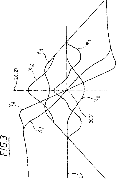
図3は図2のビーム偏向器を通過する15keV電子に対する基本軌道の経過の線図を示す。
【0027】
図1に図示された走査電子顕微鏡は粒子源(1)に後続するビーム加速器(2)を有する粒子源(1)を有する。このビーム加速器(2)を通過した後で粒子はビームガイド管(6)の電位に加速される。例えば粒子源(1)に対して10kVの電位にあるビームガイド管(6)の領域では、磁気コンデンサレンズ(3)及びこのコンデンサレンズ(3)に後続するスチグマトール(4)が設けられている。この場合、コンデンサレンズ(3)はさらに下方に後続するビーム管におけるビーム束拡大のために使用される。スチグマトール(4)には第1の静電液浸レンズ(5)が後続し、この第1の静電液浸レンズ(5)によって電子は内部ビームガイド管(7)のより高い運動エネルギに加速される。ほぼ走査電子顕微鏡の中心の内部ビームガイド管(7)の領域にはマグネットセクタ(21〜25)を有するビーム偏向器が設けられている。ビーム偏向器はこの場合粒子光学的なビームスプリッタとして作用し、このビームスプリッタは第1の光軸(OA1)に沿って入射する電子ビームをこの入射光軸(OA1)からそれた光軸(OA2)の方向に偏向する。同時に、ビーム偏向器は偏向された光軸(OA2)の方向に入射する電子ビームを出射側光軸(OA3)の方向に偏向し、この出射側光軸(OA3)は入射側光軸(OA1)と同軸に経過している。入射光軸(OA1)と偏向された光軸(OA2)との間のビーム偏向器内でのビーム偏向はこの場合第1の対称面(26)に対して対称的に行われ、偏向された光軸(OA2)と出射側光軸(OA3)との間のビーム偏向は第2の対称面(27)に対して対称的に行われる。従って、入射光軸(OA1)から偏向された光軸(OA2)への偏向の際に通過する3つのマグネットセクタ(21、22、23)は第1の偏向領域を形成し、この第1の偏向領域は第1の対称面(26)に対して対称的であり、偏向された光軸(OA2)から出射側光軸(OA3)への偏向の際に通過する3つのマグネットセクタ(23、24、25)は第2の偏向領域を形成し、この第2の偏向領域は第2の対称面(27)に対して対称的である。3つの外部偏向領域(21、23、25)における磁界方向はこの場合対称の理由から一致しておりかつ互いに平行である。これに対して、2つの中間マグネットセクタ(22、24)においては磁界方向は3つの外部マグネットセクタ(21、23、25)における磁界方向とは逆平行であり、この結果、ビーム偏向は交互の方向の部分偏向から構成されている。ビーム偏向器に関する更なる詳細は後で図2に基づいてさらに記述する。
【0028】
入射光軸(OA1)に対して偏向されたアームではビーム偏向器の後ろに静電ミラー(9)が続く。このミラー(9)によって反射された電子は再びマグネットセクタ(23)に入射するが、そこではこのマグネットセクタ(23)の最初の通過とは正反対の運動方向に基づいて正反対の方向に偏向される。次いで、これらの反射された電子は2つの後続のマグネットセクタ(24、25)を通過し、次いで光軸(3)に沿って入射光軸(OA1)に同軸にビーム偏向器から出てくる。ビーム偏向器の一度の通過の際に発生されるビーム偏向はこの場合90°に設計されており、この結果、ビーム偏向器は全体として偏向された光軸(OA2)に対して対称的である。これらのマグネットセクタはそのビーム偏向特性の他に結像特性も有するので、ミラー面(29)の像は面(30、31)に発生し、これらの面(30、31)はビーム偏向器の対称面(26、27)の近傍に存在する。理想的な調整の際にはミラー面(29)の像は精確に偏向器の対称面(26、27)に存在するが、この理想的な調整からのほんの僅かなずれは大して不利な結果をもたらさない。
【0029】
ビーム偏向器に続いて電子の運動方向にはすぐに第2の静電液浸レンズ(15)が存在し、この第2の静電液浸レンズ(15)によって電子はビームガイド管(17)のエネルギに対物レンズ(16)において制動される。同時に、この液浸レンズ(15)はミラー面(29)の像面(30)を対物レンズの回折面(28)の近傍の面に結像する。これに続いて、ビーム方向から見て前置接続、中間接続及び後置接続された単一偏向系(10、12、14)を有する2つの12極子素子(11、13)から成る系が後に続く。
【0030】
短い焦点距離及びこれから結果的に生じる対物レンズ(16)の主平面と回折面との間の空間的近さのために、ミラー面(29)が結像されている面が対物レンズ(16)の回折面(28)とぴったり一致するかどうかは比較的問題ではない。全体としてミラー面と対物レンズとの間に対物レンズ(16)の回折面(28)の2つの中間像だけが現れる。これら2つの中間像のうちの1つはミラー面(29)の中間像(30)の近傍にあり、もう1つはミラー面(29)の近傍にある。
【0031】
通常の場合には、対物レンズ(16)におけるビームガイド管の電位はコンデンサレンズ(3)の領域におけるビームガイド管(6)の電位に相応する。対物レンズ(16)によって、入射する電子ビームはこの対物レンズ(16)の焦点面(18)に集束される。この場合、対物レンズ(16)は全くの磁気的な対物レンズ又は磁気的な対物レンズと静電液浸レンズとの組み合わせのいずれかとして形成され得る。後者の場合には、静電液浸レンズは次のことによって形成される。すなわち、ビームガイド管(17)が対物レンズ(16)の内部でこの対物レンズ(16)の磁極片ギャップの高さで又はその後ろで終端し、電子がビームガイド管(17)から出た後で対物レンズ(16)の焦点面(18)の近傍に設けられた試料の電位にまで制動される。
【0032】
対物レンズの焦点面の近傍に配置された試料との相互作用によって発生する後方散乱電子又は2次電子はビームガイド管(17)のより高い電位によって再びこのビームガイド管(17)の中に戻って加速され、対物レンズ(16)とビーム偏向器との間のビーム路を正反対の方向に通過する。今や再び反転された運動方向のために、後方散乱電子及び2次電子はビーム偏向器に入る際にマグネットセクタ(25)において正反対の方向に偏向され、この結果、これらの後方散乱電子及び2次電子は入射する電子ビームからは分離される。偏向されたサイドアームにおいてビーム偏向器に後続する検出器(20)によって、2次電子も後方散乱電子も検出され得る。この検出器(20)に前置接続された静電レンズ(19)によって、異なる電位の印加により後方散乱電子と2次電子との間のエネルギ的な分離が減速ポテンシャル法に則って可能である。
【0033】
ビーム偏向器全体は全体として5つのマグネットセクタ(21〜25)から成る。この場合、全ての5つのマグネットセクタ(21〜25)はまったく凸面の外面を有し、この結果、マグネットセクタにおいて磁界を発生するために必要なコイルは比較的簡単に製造可能である。2つの内部マグネットセクタ(22、24)はこの場合同一の構造を有する。同様に全部で3つの外部マグネットセクタ(21、23、25)も同一に構成されうるが、第1のマグネットセクタ(21)に対してはこれが図2に図示されているように単に第3のマグネットセクタ(23)の半分に対して対称的な構造を有すれば十分である。同様に最後の外部マグネットセクタ(25)は一方の半分においてマグネットセクタ(23)の半分に対して対称的な構造を持ちさえすればよく、他方の半分においては場合によっては後続する検出器系に対して最適化される。個々のマグネットセクタは次のように形成される。すなわち、第1のマグネットセクタ(21)の入射エッジ(21a)は入射光軸(OA1)に対して垂直であり、第3のマグネットセクタ(23)の入射乃至は出射エッジ(23c)は偏向された光軸(OA2)に対して垂直であり、第3の偏向領域(25)の入射乃至は出射エッジ(25b)は出射光軸(OA3)に対して垂直である。この場合、入射乃至は出射エッジの傾きが、磁界方向に対して平行又は逆平行な、すなわち図2の図面平面に対して垂直な偏向磁界(B)への入射乃至は出射の際の集束作用を決定する。
【0034】
これに対して、偏向器の内部の入射及び出射エッジ(21b、22a、22b、23a、23b、24a、24b及び25a)はそれぞれ偏向された光軸に対して大きく傾斜されている。これによって、ビーム偏向器の内部において集束が磁界方向に対して平行乃至は逆平行にマグネットセクタにおいて実現され、4極子コンポーネントによるこの集束は磁界により磁界方向に対して垂直に発生される集束とちょうど同じ大きさであり、この結果、ビーム偏向器は一度の通過に対してスチグマチックな結像を発生し、このスチグマチックな結像は円形レンズの結像に相応する。
【0035】
対称性条件のためにいずれにせよ自由パラメータとしての値しか使用できない個々のマグネットセクタの間のドリフト区間長及び個々のマグネットセクタにおける偏向角度は、ビーム偏向器においては一度の通過に対する分散の無いことが要求されかつテレスコピックに入射する電子束ができるだけ弱く集束されて偏向器から離れるべきであることからもたらされる。
【0036】
図3には、15keVの運動エネルギを有する電子の図2のビーム偏向器の一度の通過に対する基本軌道が図示されている。見れば分かるように、全ての基本軌道は偏向器の内部で対称面(26、27)に対して対称に経過している。光軸(OA)に対してほぼ平行に入射するフィールド軌道xγ、yδはスチグマチックに対称面(26、27)において集束される。従って、対称面においてスチグマチックな回折像が生じる。xγ軌道の集束はこの場合マグネットセクタの双極子フィールドによって行われ、他方でyδ軌道の集束は4極子フィールドによって行われ、これらの4極子フィールドはビーム偏向器の内部のマグネットセクタの入射及び出射エッジの傾きによって生じる。同時にアパーチャ軌道xα、yβも対称面(26、27)に対して対称的な経過を有するので、ビーム偏向器全体は一度の通過に対して磁気円形レンズとして作用する。さらに分散軌道xκの経過から見て取れるように、ビーム偏向器では分散は既に一度の通過において消えてしまい、この結果、ビーム偏向器は一度の通過に対して分散をもたらさない。曲線ψ1によって図3では光軸に沿った磁界強度の経過が図示されている。個々のパスに対する偏向器の分散の無いことは、磁界強度ψ1とxα、磁界強度ψ1とxγの積の線積分が偏向器への入射及び偏向器からの出射の間に消滅するという要求、すなわち、
【0037】
【数1】
から生じる。この図に図示された実施例では2つの内部マグネットセクタ(22、24)だけが設けられている。しかし、これらの内部マグネットセクタを複数のマグネットセクタに分割することも可能であり、この結果、7個以上のマグネットセクタ及び比較可能な結像性能を有する偏向器が生じる。この場合、偏向器の各一度の通過において4つ又は相応にそれ以上のマグネットセクタが通過される。
【図面の簡単な説明】
【図1】 本発明によるミラー補正器を有する走査電子顕微鏡の原理図を示す。
【図2】 図1のビーム偏向器の拡大図を示す。
【図3】 図2のビーム偏向器を通過する15keV電子に対する基本軌道の経過の線図を示す。
【符号の説明】
1 粒子源
2 ビーム加速器
3 磁気コンデンサレンズ
4 スチグマトール
5 第1の静電液浸レンズ
6 ビームガイド管
7 内部ビームガイド管
9 静電ミラー
10 単一偏向系(10、12、14)
11 12極子素子
12 単一偏向系
13 12極子素子
14 単一偏向系
15 第2の静電液浸レンズ
16 対物レンズ
17 ビームガイド管
18 焦点面
19 静電レンズ
20 検出器
21、22、23、24、25 マグネットセクタ
21a、22a、23a、24a、25a 入射エッジ
21b、22b、23b、24b 出射エッジ
25b、23c 入射乃至は出射エッジ
26 第1の対称面
27 第2の対称面
28 回折面
29 ミラー面
30 (像)面
31 面
OA1 入射光軸
OA2 偏向された光軸
OA3 出射光軸
B 偏向磁界[0001]
The present invention relates to a particle beam system having a mirror corrector. Such a system is known for example from EP-B 10530640. Mirror correctors are used in such systems for the correction of geometric and energy dependent aberrations of particle optical components included in the system.
[0002]
The mirror corrector has a magnetic beam deflector in addition to the electrostatic mirror. Such a beam deflector is in this case a so-called for guiding the particle beam emanating from the particle source to the electrostatic mirror and guiding the particle beam reflected by this electrostatic mirror to the subsequent imaging optics. Used as a changer (Weiche) for particle beam.
[0003]
Since the beam deflector does not generate even second-order aberrations as a non-rotationally symmetric component, it is already known from EP-B 10530640 to form a corresponding beam deflector symmetrically, as a result. Has two planes of symmetry, which are perpendicular to the orbital plane of the particle beam and at the same time lie in a plane that bisects the deflection angles obtained in the individual regions of the deflector. This symmetry in the structure of the beam deflector and the simultaneous imaging of the planes of symmetry with each other by a mirror or a combination of a mirror and a field lens result in a fundamental trajectory of a particle beam symmetrical to the plane of symmetry inside the beam deflector. Is achieved, whereby the second order aberrations disappear inside the beam deflector. However, in order to guarantee this symmetrical course of the basic trajectory inside the deflector, electrostatic mirrors are provided on the one hand conjugate to the plane of symmetry of the deflector and on the other hand these planes of symmetry are connected at the same time. It is necessary to image each other at an image scale of 1: 1.
[0004]
If the intermediate image plane is imaged in these planes of symmetry in this deflector consisting of only two square sector magnets, the result is a simple and concise structure. However, coupling aberrations occur due to the large dispersion in the mirror, and this coupling aberration can only be corrected with limited quality. On the other hand, if the diffractive surface of the objective lens is imaged on the symmetry plane of the deflector, such coupling aberration does not occur because almost no dispersion occurs in the mirror. Indeed, this mode of operation produces dispersion in the image, which must be noticeable only after passing through the deflector twice. However, the large focal length of the deflector requires a reduction in the beam bundle diameter, which can only be achieved with a very large length or at least a two-stage objective lens system and likewise at least a two-stage mirror system. Can be done.
[0005]
EP 0 530 640 further describes a deflector that does not produce dispersion for a single pass of the particle beam. However, it has either three different magnetic fields with additional superimposed electrostatic fields or a magnet sector with a partially concave outer surface. However, the concave outer surface of the magnet sector requires the formation of a corresponding concave surface of the magnet coil, which also causes manufacturing technology problems, especially in mass production.
[0006]
It is an object of the present invention to provide a particle beam system having a mirror corrector that allows a generally simplified and more compact structure.
[0007]
This object is solved by a particle beam system having the configuration of claim 1. Advantageous embodiments of the invention result from the features of the dependent claims.
[0008]
Like the system described in EP-B 1530640 cited at the outset, the system of the invention also has a beam deflector, which does not provide dispersion for a single pass. In this case, the fact that no dispersion occurs means that the dispersion of the deflector is so small that it is feasible that no dispersion occurs by optimal adjustment of the components of the deflector. .
[0009]
In addition to providing no dispersion, the deflector has quadrupole or quadrupole components, which are selected as follows. That is, a maximum of two conjugate planes with respect to the diffractive surface of the objective lens in the entire trajectory between the first exit from the deflector and the first exit from the objective lens, that is, between the diffractive surfaces of the objective lens An image plane is selected to occur.
[0010]
Since the deflector is sufficiently telescopic, the particle beam emerging from the intersection of the planes of symmetry with the optical axis passes in parallel or only slightly converges outside the deflector.
[0011]
The plane conjugate to the diffractive surface of the objective lens preferably coincides with the plane of the electrostatic mirror, i.e. the plane in which the inversion points for all trajectories are present on the basis of a reverse electrostatic field (das elektrostatische Gegenfeld). This state is adjusted by an additional field lens.
[0012]
Like known beam deflectors, the beam deflector according to the invention also advantageously has a first symmetry plane in the first region and a second symmetry surface in the second region, so that Each deflection is performed symmetrically with respect to these planes of symmetry.
[0013]
In each of the two symmetry regions, the beam deflector of the present invention each has at least two outer magnet sectors and at least one inner magnet sector. There is provided an internal magnet sector inserted between an external magnet sector existing on the incident side and the exit side of the beam deflector and an external magnet sector on the incident side and the exit side of the beam deflector. A drift zone is more advantageously provided between the outer magnet sector and the inner magnet sector in an intermediate space without a magnetic field.
[0014]
Since a drift section is provided between the magnet sectors, the entrance and exit edges have a tilt deflected with respect to the optical axis, whereby focusing is performed parallel to the direction of the magnetic field. This focusing by the quadrupole component at the entrance and exit edges is in this case coincident with the focusing perpendicular to the direction of the magnetic field generated by the deflection field, so that the deflector as a whole forms a stigmatic image like a circular lens. appear. However, a quadrupole element can also be provided in the deflector or just before and after the deflector instead of or in addition to the tilted entrance and exit edge.
[0015]
The deflection angles in the individual magnet sectors are chosen such that no total dispersion occurs after a single pass through the deflector. Coupling aberrations caused by the interaction between the dispersion and the chromatic or spherical aberration of the electrostatic mirrors post-connected to the deflector are thereby avoided. Furthermore, no dispersion occurs in the intermediate image, and this dispersion is compensated very accurately in the second pass of the deflector. Such a beam deflector without dispersion for a single pass is realized when the magnetic field in the intermediate magnet sector is antiparallel to the magnetic field direction in the external magnet sector.
[0016]
In a further advantageous embodiment, the magnetic fields are equal in magnitude in the inner magnet sector and in both outer magnet sectors. This allows main coils with the same number of turns to be used in series to generate different magnetic fields, which also results in a relatively low demand on the stability of the current source.
[0017]
Furthermore, the beam deflector is preferably completely magnetic, i.e. no electrostatic field is provided for the deflection of the particle beam or for focusing perpendicular to the deflection direction.
[0018]
Beam tilting due to the incidence and exit edge tilt of the external magnet sector relative to the optical axis and the magnetic field in the magnet sector is preferably such that particles incident parallel to the optical axis are focused near or close to the plane of symmetry of the deflector. Selected to be. This achieves the following: That is, the field trajectory outside the deflector (die Feldbahnen) passes parallel or nearly parallel to the optical axis, so that the intersection of the field trajectory and the optical axis is away from the entrance and exit edges of the deflector. This requires only one additional field lens to image the field trajectory, but additional imaging of the axial trajectory that would require further intermediate imaging. Is not necessary.
[0019]
The corresponding field lens is preferably formed as an electrostatic immersion lens with an intermediate electrode, resulting in an overall imaging. As a result, the beam deflector can be operated at a constant potential even with a varying columnar potential (Saeulenpotential). However, other types of magnetic lenses and / or electrostatic lenses are possible.
[0020]
Furthermore, advantageously one or two octupole elements or higher order elements having at least a quadrupole winding, a hexapole winding and an octupole winding between the beam deflector and the objective lens, in particular A 12-pole element is provided. Additionally, the one or more 12-pole elements may have dipole windings. However, instead of these dipole windings, two or three separate individual deflection systems are also possible. One or more twelve-pole elements can be used in this case as an aufgeblasen stigmator, which assures overall stigmatic imaging. One or more 12-pole elements can in this case be formed as air-core coils. It is also conceivable to arrange two twelve-pole elements between the deflector and the objective lens without further deflection systems. In this case, however, all 12 poles of the two 12-pole elements must be able to be controlled separately and independently of each other, i.e. current can be applied. Instead, between the beam deflector and the first 12-pole element following this beam deflector, between the two 12-pole elements and behind the second 12-pole element as viewed from the beam direction. It is also conceivable to provide individual deflection systems. A separate deflection system is used in this case for beam adjustment.
[0021]
Two electrostatic individual deflectors should be provided between the beam deflector and the electrostatic mirror. Alternatively, multipole elements may be placed between the deflector and the electrostatic mirror in an electromagnetic configuration, especially when there is insufficient structural space between the objective lens and the beam deflector. sell.
[0022]
Furthermore, it is advantageous that the stigmatol is deflected with respect to the particle source in order to adjust the imaging situation, in particular residual distortion and astigmatism, between the particle source and the electrostatic mirror in the deflection region of the deflector by changing the stigmatol. Provide between the container.
[0023]
It has proved advantageous if the particles have a minimum energy that does not drop further between the beam deflector and the electrostatic mirror. Therefore, particularly in applications with low kinetic energy of particles, it is advantageous to provide electrostatic immersion lenses between the particle source and the deflector and between the deflector and the objective lens, respectively. The immersion lens increases the kinetic energy of the particles before entering the deflector and reduces it again after exiting the deflector. Thereby, the deflector can be operated with a constant kinetic energy of electrons in the region of the deflector, ie with a constant deflection field.
[0024]
The total deflection in one pass of the deflector is preferably 90 °, so that the outgoing optical axis passes coaxially with the incident optical axis after two passes of the deflector due to intermediate particle reflections. .
[0025]
The entire system with the mirror corrector is advantageously operated so that the chromatic and spherical aberration of the entire imaging system is corrected between the particle source and the objective lens at the same time. This increases the resolution of the corresponding particle beam system as a whole.
[0026]
Next, details of the present invention will be described in detail based on the embodiments shown in the drawings. Respectively,
FIG. 1 shows a principle diagram of a scanning electron microscope having a mirror corrector according to the present invention.
FIG. 2 shows an enlarged view of the beam deflector of FIG.
FIG. 3 shows a diagram of the basic trajectory for 15 keV electrons passing through the beam deflector of FIG.
[0027]
The scanning electron microscope illustrated in FIG. 1 has a particle source (1) having a beam accelerator (2) following the particle source (1). After passing through the beam accelerator (2), the particles are accelerated to the potential of the beam guide tube (6). For example, in the region of the beam guide tube (6) at a potential of 10 kV with respect to the particle source (1), a magnetic condenser lens (3) and a stigmator (4) following the condenser lens (3) are provided. In this case, the condenser lens (3) is used for expanding the beam bundle in the beam tube following further downward. The stigmator (4) is followed by a first electrostatic immersion lens (5) by which electrons are accelerated to a higher kinetic energy of the internal beam guide tube (7). Is done. A beam deflector having magnet sectors (21 to 25) is provided in the region of the internal beam guide tube (7) substantially at the center of the scanning electron microscope. The beam deflector in this case acts as a particle-optical beam splitter, which emits an electron beam incident along the first optical axis (OA1) from the incident optical axis (OA1) (OA2). ) In the direction of). At the same time, the beam deflector deflects the electron beam incident in the direction of the deflected optical axis (OA2) in the direction of the emission side optical axis (OA3), and this emission side optical axis (OA3) is the incident side optical axis (OA1). ) And coaxial. The beam deflection in the beam deflector between the incident optical axis (OA1) and the deflected optical axis (OA2) is in this case performed symmetrically with respect to the first symmetry plane (26) and deflected. Beam deflection between the optical axis (OA2) and the outgoing optical axis (OA3) is performed symmetrically with respect to the second symmetry plane (27). Accordingly, the three magnet sectors (21, 22, 23) that pass when deflecting from the incident optical axis (OA1) to the deflected optical axis (OA2) form a first deflection region, and this first deflection area is formed. The deflection area is symmetric with respect to the first symmetry plane (26), and passes through three magnet sectors (23, 23) that pass when deflecting from the deflected optical axis (OA2) to the outgoing optical axis (OA3). 24, 25) form a second deflection region, which is symmetrical with respect to the second plane of symmetry (27). The magnetic field directions in the three external deflection regions (21, 23, 25) are in this case coincident for symmetry reasons and parallel to each other. On the other hand, in the two intermediate magnet sectors (22, 24), the magnetic field direction is antiparallel to the magnetic field directions in the three external magnet sectors (21, 23, 25). It consists of partial deflections in direction. Further details regarding the beam deflector will be further described later with reference to FIG.
[0028]
In the arm deflected with respect to the incident optical axis (OA1), an electrostatic mirror (9) follows the beam deflector. The electrons reflected by this mirror (9) are incident on the magnet sector (23) again, where they are deflected in the opposite direction based on the direction of motion opposite to the first pass of the magnet sector (23). . These reflected electrons then pass through two subsequent magnet sectors (24, 25) and then emerge from the beam deflector coaxially with the incident optical axis (OA1) along the optical axis (3). The beam deflection generated during one pass of the beam deflector is in this case designed to be 90 °, so that the beam deflector as a whole is symmetrical with respect to the deflected optical axis (OA2). . Since these magnet sectors have not only their beam deflection characteristics but also imaging characteristics, the image of the mirror surface (29) is generated on the planes (30, 31), and these planes (30, 31) are generated by the beam deflector. It exists in the vicinity of the symmetry plane (26, 27). In the case of an ideal adjustment, the image of the mirror surface (29) is exactly in the plane of symmetry (26, 27) of the deflector, but a slight deviation from this ideal adjustment will have a very disadvantageous result. Will not bring.
[0029]
A second electrostatic immersion lens (15) immediately follows the beam deflector in the direction of movement of the electrons, and the second electrostatic immersion lens (15) allows the electrons to pass through the beam guide tube (17). Is braked in the objective lens (16). At the same time, the immersion lens (15) forms an image on the image plane (30) of the mirror surface (29) on a plane in the vicinity of the diffractive surface (28) of the objective lens. This is followed by a system consisting of two 12-pole elements (11, 13) with a single deflection system (10, 12, 14) connected in front, intermediate and back connection as viewed from the beam direction. Continue.
[0030]
Due to the short focal length and the resulting spatial proximity between the principal plane and the diffractive surface of the objective lens (16) resulting therefrom, the surface on which the mirror surface (29) is imaged is the objective lens (16). It is relatively unimportant whether it exactly matches the diffractive surface (28). Overall, only two intermediate images of the diffractive surface (28) of the objective lens (16) appear between the mirror surface and the objective lens. One of these two intermediate images is in the vicinity of the intermediate image (30) on the mirror surface (29) and the other is in the vicinity of the mirror surface (29).
[0031]
In the usual case, the potential of the beam guide tube in the objective lens (16) corresponds to the potential of the beam guide tube (6) in the region of the condenser lens (3). The incident electron beam is focused on the focal plane (18) of the objective lens (16) by the objective lens (16). In this case, the objective lens (16) can be formed either as a complete magnetic objective lens or as a combination of a magnetic objective lens and an electrostatic immersion lens. In the latter case, the electrostatic immersion lens is formed by: That is, after the beam guide tube (17) terminates in the objective lens (16) at the height of or behind the pole piece gap of the objective lens (16), and after the electrons exit the beam guide tube (17). Thus, braking is performed up to the potential of the sample provided in the vicinity of the focal plane (18) of the objective lens (16).
[0032]
Backscattered electrons or secondary electrons generated by the interaction with the sample arranged in the vicinity of the focal plane of the objective lens are returned to the beam guide tube (17) again by the higher potential of the beam guide tube (17). And pass through the beam path between the objective lens (16) and the beam deflector in the opposite direction. Due to the now reversed direction of motion, backscattered electrons and secondary electrons are deflected in the opposite direction in the magnet sector (25) upon entering the beam deflector, so that these backscattered electrons and secondary electrons The electrons are separated from the incident electron beam. Both secondary and backscattered electrons can be detected by the detector (20) following the beam deflector in the deflected side arm. The electrostatic lens (19) connected in front to the detector (20) enables energetic separation between backscattered electrons and secondary electrons by applying different potentials in accordance with the deceleration potential method. .
[0033]
The whole beam deflector consists of five magnet sectors (21-25) as a whole. In this case, all five magnet sectors (21-25) have a completely convex outer surface, so that the coils necessary for generating a magnetic field in the magnet sector can be manufactured relatively easily. The two internal magnet sectors (22, 24) have the same structure in this case. Similarly, a total of three external magnet sectors (21, 23, 25) can be configured identically, but for the first magnet sector (21) this is simply the third as shown in FIG. It is sufficient to have a symmetrical structure with respect to half of the magnet sector (23). Similarly, the last outer magnet sector (25) only needs to have a symmetrical structure in one half with respect to the half of the magnet sector (23), in the other half possibly in the subsequent detector system. Optimized for. Individual magnet sectors are formed as follows. That is, the incident edge (21a) of the first magnet sector (21) is perpendicular to the incident optical axis (OA1), and the incident or exit edge (23c) of the third magnet sector (23) is deflected. The incident or exit edge (25b) of the third deflection region (25) is perpendicular to the exit optical axis (OA3). In this case, the inclination of the incident or outgoing edge is parallel or anti-parallel to the magnetic field direction, that is, the focusing action at the time of incident or outgoing to the deflection magnetic field (B) perpendicular to the drawing plane of FIG. To decide.
[0034]
On the other hand, the entrance and exit edges (21b, 22a, 22b, 23a, 23b, 24a, 24b, and 25a) inside the deflector are largely inclined with respect to the deflected optical axis. As a result, focusing inside the beam deflector is realized in the magnet sector either parallel or antiparallel to the magnetic field direction, and this focusing by the quadrupole component is exactly the same as the focusing generated perpendicular to the magnetic field direction by the magnetic field. As a result of this, the beam deflector generates a stigmatic image for a single pass, which corresponds to the image of a circular lens.
[0035]
The drift section length between individual magnet sectors and the deflection angle at each magnet sector, which can only be used as free parameters anyway due to symmetry conditions, should not be dispersed for a single pass in the beam deflector. Resulting from the fact that the electron flux incident on the telescopic should be focused as weakly as possible and away from the deflector.
[0036]
FIG. 3 shows the basic trajectory for a single pass of the beam deflector of FIG. 2 of electrons having a kinetic energy of 15 keV. As can be seen, all the basic trajectories pass symmetrically with respect to the plane of symmetry (26, 27) inside the deflector. The field trajectories xγ and yδ incident substantially parallel to the optical axis (OA) are stigmatically focused on the symmetry planes (26, 27). Accordingly, a stigmatic diffraction image is generated on the symmetry plane. The focusing of the xγ trajectory is in this case performed by the dipole field of the magnet sector, while the focusing of the yδ trajectory is performed by the quadrupole field, which is the incoming and outgoing edges of the magnet sector inside the beam deflector. Caused by the slope of At the same time, since the aperture trajectories xα and yβ have a symmetrical course with respect to the symmetry plane (26, 27), the entire beam deflector acts as a magnetic circular lens for one pass. Further, as can be seen from the course of the dispersion trajectory xκ, the dispersion already disappears in one pass in the beam deflector, and as a result, the beam deflector does not cause dispersion in one pass. The curve ψ1 shows the course of the magnetic field strength along the optical axis in FIG. The absence of deflection of the deflectors for the individual paths is a requirement that the line integral of the product of the magnetic field strengths ψ1 and xα and the magnetic field strengths ψ1 and xγ disappears between the incidence on the deflector and the exit from the deflector, ie ,
[0037]
[Expression 1]
Arise from. In the embodiment illustrated in this figure, only two internal magnet sectors (22, 24) are provided. However, it is also possible to divide these internal magnet sectors into a plurality of magnet sectors, resulting in more than seven magnet sectors and deflectors with comparable imaging performance. In this case, four or correspondingly more magnetic sectors are passed in each pass of the deflector.
[Brief description of the drawings]
FIG. 1 shows a principle diagram of a scanning electron microscope having a mirror corrector according to the present invention.
2 shows an enlarged view of the beam deflector of FIG.
FIG. 3 shows a diagram of the basic trajectory for 15 keV electrons passing through the beam deflector of FIG.
[Explanation of symbols]
DESCRIPTION OF SYMBOLS 1
DESCRIPTION OF
Claims (12)
前記ミラー補正器は、静電ミラー(9)を有し、さらにビーム路において前記粒子源(1)と前記静電ミラー(9)との間にならびに該静電ミラー(9)と前記対物レンズ(16)との間に磁気ビーム偏向器を有し、
該磁気ビーム偏向器は、少なくとも3つの外部マグネットセクタ(21,23,25)と少なくとも2つの内部マグネットセクタ(22,24)から構成されており、
粒子源(1)と静電ミラー(9)との間では2つの外部マグネットセクタ(21,23)がこれらの外部マグネットセクタ(21,23)の間にある1つの内部マグネットセクタ(22)を有し、ならびに、前記ミラー(9)と対物レンズ(16)との間では2つの外部マグネットセクタ(23,25)がこれらの外部マグネットセクタ(23,25)の間にある1つの内部マグネットセクタ(24)を有し、
内部マグネットセクタ(22,24)における磁界方向は外部マグネットセクタ(21,23,25)における磁界方向とは平行であるが、逆方向であり、内部マグネットセクタにおける磁界強度と外部マグネットセクタにおける磁界強度とは、磁気ビーム偏向器を通過する粒子ビームに分散が生じないように選択されており、
外部および内部マグネットセクタ(21,22,23,24,25)は入射エッジおよび出射エッジ(21b、22a、22b、23a、23b、24a、24b、25a)を有し、該入射エッジおよび出射エッジは粒子ビームの光軸に対して傾斜しており、これにより前記入射エッジおよび出射エッジに4極子及び / 又は4極子コンポーネントが形成され、
静電ミラー(9)に前置された外部マグネットセクタ(23)からの最初の出射と前記対物レンズ(16)からの最初の出射との間の全軌道経過において該対物レンズ(16)の回折面(28)に対する最大で2つの共役面(29,30)しか生じないように前記4極子及び/又は4極子コンポーネントは決定されている、粒子ビームシステム。In a particle beam system comprising a particle source (1), a mirror corrector (9, 21-25) and an objective lens (16),
The mirror corrector includes an electrostatic mirror (9), and further between the particle source (1) and the electrostatic mirror (9) in the beam path, and the electrostatic mirror (9) and the objective lens. has a magnetic beam deflector between the (16),
The magnetic beam deflector is composed of at least three external magnet sectors (21, 23, 25) and at least two internal magnet sectors (22, 24).
Between the particle source (1) and the electrostatic mirror (9), two external magnet sectors (21, 23) are connected to one internal magnet sector (22) between these external magnet sectors (21, 23). And one internal magnet sector with two external magnet sectors (23, 25) between the external magnet sectors (23, 25) between the mirror (9) and the objective lens (16). (24)
The magnetic field direction in the internal magnet sector (22, 24) is parallel to the magnetic field direction in the external magnet sector (21, 23, 25), but in the opposite direction, and the magnetic field strength in the internal magnet sector and the magnetic field strength in the external magnet sector. Is selected so that no dispersion occurs in the particle beam passing through the magnetic beam deflector,
The outer and inner magnet sectors (21, 22, 23, 24, 25) have incident and outgoing edges (21b, 22a, 22b, 23a, 23b, 24a, 24b, 25a), the incident and outgoing edges being Tilted with respect to the optical axis of the particle beam, thereby forming quadrupoles and / or quadrupole components at the entrance and exit edges ;
Diffraction of the objective lens (16) during the entire trajectory between the first exit from the external magnet sector (23) placed in front of the electrostatic mirror (9) and the first exit from the objective lens (16) up the so occur only two conjugate planes (29, 30) quadrupole and / or quadrupole components are determined, the particle element beam system with respect to the surface (28).
Applications Claiming Priority (2)
| Application Number | Priority Date | Filing Date | Title |
|---|---|---|---|
| DE10107910A DE10107910A1 (en) | 2001-02-20 | 2001-02-20 | Particle beam system with a mirror corrector |
| PCT/EP2002/001553 WO2002067286A2 (en) | 2001-02-20 | 2002-02-14 | Particle beam system comprising a mirror corrector |
Publications (2)
| Publication Number | Publication Date |
|---|---|
| JP2004519084A JP2004519084A (en) | 2004-06-24 |
| JP4004961B2 true JP4004961B2 (en) | 2007-11-07 |
Family
ID=7674707
Family Applications (1)
| Application Number | Title | Priority Date | Filing Date |
|---|---|---|---|
| JP2002566518A Expired - Lifetime JP4004961B2 (en) | 2001-02-20 | 2002-02-14 | Particle beam system with mirror corrector |
Country Status (6)
| Country | Link |
|---|---|
| US (1) | US6855939B2 (en) |
| EP (1) | EP1362361B1 (en) |
| JP (1) | JP4004961B2 (en) |
| CZ (1) | CZ301532B6 (en) |
| DE (2) | DE10107910A1 (en) |
| WO (1) | WO2002067286A2 (en) |
Families Citing this family (71)
| Publication number | Priority date | Publication date | Assignee | Title |
|---|---|---|---|---|
| DE10235981B9 (en) * | 2002-08-06 | 2009-01-22 | Leo Elektronenmikroskopie Gmbh | Particle-optical device and electron microscope |
| US7022987B2 (en) | 2001-02-20 | 2006-04-04 | Carl Zeiss Nis Gmbh | Particle-optical arrangements and particle-optical systems |
| DE10159454B4 (en) * | 2001-12-04 | 2012-08-02 | Carl Zeiss Nts Gmbh | Corrector for correcting first-order, first-degree chromatic aberrations |
| DE10235456B4 (en) * | 2002-08-02 | 2008-07-10 | Leo Elektronenmikroskopie Gmbh | electron microscopy system |
| WO2005024881A2 (en) | 2003-09-05 | 2005-03-17 | Carl Zeiss Smt Ag | Particle-optical systems, components and arrangements |
| US6878937B1 (en) * | 2004-02-10 | 2005-04-12 | Kla-Tencor Technologies Corporation | Prism array for electron beam inspection and defect review |
| US7348566B2 (en) * | 2006-02-28 | 2008-03-25 | International Business Machines Corporation | Aberration-correcting cathode lens microscopy instrument |
| EP1883094B1 (en) * | 2006-07-24 | 2012-05-02 | ICT, Integrated Circuit Testing Gesellschaft für Halbleiterprüftechnik mbH | Charged particle beam device and method for inspecting specimen |
| DE102008001812B4 (en) * | 2008-05-15 | 2013-05-29 | Carl Zeiss Microscopy Gmbh | Positioning device for a particle beam device |
| JP5250350B2 (en) * | 2008-09-12 | 2013-07-31 | 株式会社日立ハイテクノロジーズ | Charged particle beam application equipment |
| DE102008064696B4 (en) * | 2008-12-23 | 2022-01-27 | Carl Zeiss Microscopy Gmbh | Magnet array particle optical device and its use for imaging or illumination |
| DE102009016861A1 (en) | 2009-04-08 | 2010-10-21 | Carl Zeiss Nts Gmbh | particle beam |
| US8129693B2 (en) * | 2009-06-26 | 2012-03-06 | Carl Zeiss Nts Gmbh | Charged particle beam column and method of operating same |
| DE102009052392A1 (en) | 2009-11-09 | 2011-12-15 | Carl Zeiss Nts Gmbh | SACP process and particle-optical system for carrying out such a process |
| EP2511936B1 (en) * | 2011-04-13 | 2013-10-02 | Fei Company | Distortion free stigmation of a TEM |
| DE102011076893A1 (en) | 2011-06-01 | 2012-12-06 | Carl Zeiss Nts Gmbh | Method and particle beam device for focusing a particle beam |
| DE102012215945A1 (en) | 2012-09-07 | 2014-03-13 | Carl Zeiss Microscopy Gmbh | Particle beam apparatus and method for operating a particle beam device |
| JP5493029B2 (en) * | 2013-04-12 | 2014-05-14 | 株式会社日立ハイテクノロジーズ | Charged particle beam application equipment |
| US8841631B1 (en) * | 2013-06-26 | 2014-09-23 | Varian Semiconductor Equipment Associates, Inc. | Apparatus and techniques for controlling ion angular spread |
| US9312093B1 (en) | 2014-06-27 | 2016-04-12 | Carl Zeiss Microscopy Gmbh | Particle beam device comprising an electrode unit |
| US9595417B2 (en) * | 2014-12-22 | 2017-03-14 | ICT Integrated Circuit Testing Gesellschaft für Halbleiterprüftechnik mbH | High resolution charged particle beam device and method of operating the same |
| JP6339734B2 (en) * | 2015-02-18 | 2018-06-06 | 株式会社日立製作所 | Charged particle beam application apparatus and aberration corrector |
| DE102015108245A1 (en) | 2015-05-26 | 2016-12-01 | Carl Zeiss Microscopy Gmbh | Method for producing an image of an object with a particle beam device and particle beam device for carrying out the method |
| DE102015210893B4 (en) | 2015-06-15 | 2019-05-09 | Carl Zeiss Microscopy Gmbh | Analysis device for analyzing the charged particle energy and particle beam device with an analysis device |
| US9472373B1 (en) * | 2015-08-17 | 2016-10-18 | ICT Integrated Circuit Testing Gesellschaft für Halbleiterprüftechnik mbH | Beam separator device, charged particle beam device and methods of operating thereof |
| US9620331B1 (en) | 2015-11-19 | 2017-04-11 | Carl Zeiss Microscopy Ltd. | Method for analyzing an object and charged particle beam device for carrying out the method |
| EP3176808B1 (en) | 2015-12-03 | 2019-10-16 | Carl Zeiss Microscopy Ltd. | Method for detecting charged particles and particle beam device for carrying out the method |
| EP3236486A1 (en) | 2016-04-22 | 2017-10-25 | Carl Zeiss Microscopy GmbH | Method for generating a composite image of an object and particle beam device for carrying out the method |
| DE102016208689B4 (en) | 2016-05-20 | 2018-07-26 | Carl Zeiss Microscopy Gmbh | A method of generating an image of an object and / or a representation of data about the object, and computer program product and particle beam apparatus for performing the method |
| DE102017201706B4 (en) | 2017-02-02 | 2025-10-23 | Carl Zeiss Microscopy Gmbh | Particle beam device with an imaging device for imaging an object and for imaging a structural unit in the particle beam device and method for operating the particle beam device |
| DE102017203553A1 (en) | 2017-03-04 | 2018-09-06 | Carl Zeiss Microscopy Gmbh | Object preparation device and particle beam device with an object preparation device and method for operating the particle beam device |
| DE102017203554A1 (en) * | 2017-03-04 | 2018-09-06 | Carl Zeiss Microscopy Gmbh | Object preparation device and particle beam device with an object preparation device and method for operating the particle beam device |
| DE102018202728B4 (en) | 2018-02-22 | 2019-11-21 | Carl Zeiss Microscopy Gmbh | Method for operating a particle beam device, computer program product and particle beam device for carrying out the method |
| DE102018010335B3 (en) | 2018-02-22 | 2023-08-10 | Carl Zeiss Microscopy Gmbh | Method for operating a particle beam device, computer program product and particle beam device for carrying out the method |
| DE102018203096B9 (en) | 2018-03-01 | 2020-02-27 | Carl Zeiss Microscopy Gmbh | Method for operating a printing system for a device for imaging, analyzing and / or processing an object and device for carrying out the method |
| DE102018207645B9 (en) | 2018-05-16 | 2022-05-05 | Carl Zeiss Microscopy Gmbh | Method for operating a particle beam generator for a particle beam device, computer program product and particle beam device with a particle beam generator |
| DE102018216968B9 (en) | 2018-10-02 | 2021-01-28 | Carl Zeiss Microscopy Gmbh | Method for setting a position of a component of a particle beam device, computer program product and particle beam device for performing the method |
| DE102018010383A1 (en) | 2018-10-02 | 2020-07-23 | Carl Zeiss Microscopy Gmbh | Method for setting a position of a component of a particle beam device, computer program product and particle beam device for carrying out the method |
| US10658152B1 (en) | 2018-10-04 | 2020-05-19 | Carl Zeiss Microscopy Gmbh | Method for controlling a particle beam device and particle beam device for carrying out the method |
| DE102018222522A1 (en) | 2018-12-20 | 2020-06-25 | Carl Zeiss Microscopy Gmbh | Method for operating a gas supply device and gas supply device for carrying out the method and particle beam device with a gas supply device |
| DE102019004124B4 (en) | 2019-06-13 | 2024-03-21 | Carl Zeiss Multisem Gmbh | Particle beam system for the azimuthal deflection of individual particle beams and its use and method for azimuth correction in a particle beam system |
| DE102019208661A1 (en) * | 2019-06-13 | 2020-12-17 | Carl Zeiss Microscopy Gmbh | Method for operating a particle beam device and particle beam device for carrying out the method |
| DE102019214936A1 (en) * | 2019-09-27 | 2021-04-01 | Carl Zeiss Microscopy Gmbh | Method for determining a material composition of an object with a particle beam device, computer program product and particle beam device for carrying out the method and system with a particle beam device |
| DE102019216791B4 (en) | 2019-10-30 | 2023-08-10 | Carl Zeiss Microscopy Gmbh | Method for operating a particle beam device and/or a light microscope, computer program product and particle beam device and light microscope for carrying out the method |
| DE102020102314B4 (en) | 2020-01-30 | 2022-02-10 | Carl Zeiss Microscopy Gmbh | Object receiving container, object holding system with an object receiving container, blasting device and device with an object receiving container or an object holding system, and methods for examining, analyzing and/or processing an object |
| DE102020102854B4 (en) | 2020-02-05 | 2024-06-06 | Carl Zeiss Microscopy Gmbh | Particle beam device |
| DE102020103339A1 (en) | 2020-02-10 | 2021-08-12 | Carl Zeiss Microscopy Gmbh | Method for operating a particle beam device, computer program product and particle beam device for carrying out the method |
| DE102020104704A1 (en) | 2020-02-21 | 2021-08-26 | Carl Zeiss Microscopy Gmbh | Method for processing images, computer program product, image processing device and beam device for carrying out the method |
| DE102020111151B4 (en) | 2020-04-23 | 2023-10-05 | Carl Zeiss Microscopy Gmbh | Method for ventilating and pumping out a vacuum chamber of a particle beam device, computer program product and particle beam device for carrying out the method |
| DE102020112220B9 (en) | 2020-05-06 | 2022-05-25 | Carl Zeiss Microscopy Gmbh | Particle beam device for removing at least one material from a material unit and arranging the material on an object |
| DE102020122535B4 (en) | 2020-08-28 | 2022-08-11 | Carl Zeiss Microscopy Gmbh | Method for operating a blasting device, computer program product and blasting device for carrying out the method |
| US11380519B1 (en) | 2020-11-05 | 2022-07-05 | Carl Zeiss Microscopy Gmbh | Operating a particle beam generator for a particle beam device |
| DE102021102900B4 (en) | 2021-02-08 | 2022-11-17 | Carl Zeiss Microscopy Gmbh | Method for operating a particle beam device, computer program product and particle beam device for carrying out the method |
| JP7381515B2 (en) * | 2021-03-31 | 2023-11-15 | 株式会社日立ハイテク | Electron beam application equipment |
| DE102021110948B4 (en) | 2021-04-28 | 2023-09-28 | Carl Zeiss Microscopy Gmbh | Method for processing an object with a material processing device, computer program product and material processing device for carrying out the method |
| DE102021112503B4 (en) * | 2021-05-12 | 2025-03-27 | Carl Zeiss Microscopy Gmbh | Particle beam device with a deflection unit |
| DE102021113930A1 (en) | 2021-05-28 | 2022-12-01 | Carl Zeiss Microscopy Gmbh | Method for generating an image of an object and/or a representation of data about the object, computer program product and particle beam device for carrying out the method |
| DE202021004363U1 (en) | 2021-05-28 | 2023-12-04 | Carl Zeiss Microscopy Gmbh | Particle beam device for generating an image of an object and/or a representation of data about the object, and computer program product for generating the image of the object and/or the representation of data about the object |
| DE102021128117B4 (en) | 2021-10-28 | 2025-02-13 | Carl Zeiss Microscopy Gmbh | Method for producing a sample on an object, computer program product and material processing device for carrying out the method |
| TWI842136B (en) | 2021-10-28 | 2024-05-11 | 德商卡爾蔡司Smt有限公司 | High resolution, low energy electron microscope for providing topography information and method of mask inspection |
| DE102021212978A1 (en) | 2021-11-18 | 2023-05-25 | Carl Zeiss Smt Gmbh | Method for imaging with a scanning electron microscope and scanning electron microscope for carrying out the method |
| DE102021132832A1 (en) | 2021-12-13 | 2023-06-15 | Carl Zeiss Microscopy Gmbh | Gas supply device, particle beam device with a gas supply device and method for operating the gas supply device and the particle beam device |
| DE102021132833A1 (en) | 2021-12-13 | 2023-06-15 | Carl Zeiss Microscopy Gmbh | Gas supply device, system with a gas supply device and particle beam device with a gas supply device or the system |
| DE102021132834B4 (en) | 2021-12-13 | 2024-08-08 | Carl Zeiss Microscopy Gmbh | Gas reservoir, gas supply device with a gas reservoir and particle beam device with a gas supply device |
| DE102022119041A1 (en) | 2022-07-28 | 2024-02-08 | Carl Zeiss Microscopy Gmbh | Method for attaching an object to a manipulator and moving the object in a particle beam device, computer program product and particle beam device |
| DE102022119042A1 (en) | 2022-07-28 | 2024-02-08 | Carl Zeiss Microscopy Gmbh | Method for attaching an object to a manipulator and/or to an object holder in a particle beam device, computer program product, particle beam device and device for attaching and moving an object |
| DE102022120496B4 (en) * | 2022-08-12 | 2025-05-28 | Carl Zeiss Multisem Gmbh | Particle-optical arrangement, in particular a multi-beam particle microscope, with a magnet arrangement for separating a primary and a secondary particle-optical beam path |
| DE102022130985A1 (en) | 2022-11-23 | 2024-05-23 | Carl Zeiss Microscopy Gmbh | Method for operating a particle beam device, computer program product and particle beam device for carrying out the method |
| DE102022132951B4 (en) | 2022-12-12 | 2024-09-26 | Carl Zeiss Microscopy Gmbh | Method for determining a position of an object in a blasting device, computer program product and blasting device for carrying out the method |
| DE102023108279A1 (en) | 2023-03-31 | 2024-10-02 | Carl Zeiss Microscopy Gmbh | Method for operating a particle beam device, computer program product and particle beam device for carrying out the method |
| DE102023120127B4 (en) | 2023-07-28 | 2025-03-27 | Carl Zeiss Multisem Gmbh | Particle-optical arrangement, in particular multi-beam particle microscope, with a magnet arrangement for separating a primary and a secondary particle-optical beam path with improved performance |
Family Cites Families (20)
| Publication number | Priority date | Publication date | Assignee | Title |
|---|---|---|---|---|
| GB458015A (en) * | 1935-05-20 | 1936-12-10 | British Thomson Houston Co Ltd | Improvements in and relating to the control of electronic rays |
| FR2036373A5 (en) * | 1969-03-12 | 1970-12-24 | Thomson Csf | |
| US4107526A (en) * | 1976-03-22 | 1978-08-15 | Minnesota Mining And Manufacturing Company | Ion scattering spectrometer with modified bias |
| US4367406A (en) * | 1981-01-13 | 1983-01-04 | Trustees Of Boston University | Cylindrical mirror electrostatic energy analyzer free of third-order angular aberrations |
| JPS63276860A (en) * | 1987-05-07 | 1988-11-15 | Nissin Electric Co Ltd | Surface analyzing device |
| DE3931970A1 (en) | 1989-09-25 | 1991-04-04 | Roethele S | Sector field deflection system for LV electron microscope - has several magnet sectors with uniformly excited outer pole shoe, enclosing several, identical excited inner pole shoes |
| DE4041495A1 (en) * | 1990-12-22 | 1992-06-25 | Zeiss Carl Fa | ELECTRONIC ENERGY FILTER, PREFERRED ALPHA OR OMEGA TYPE |
| DE4129403A1 (en) * | 1991-09-04 | 1993-03-11 | Zeiss Carl Fa | IMAGING SYSTEM FOR RADIATION OF CHARGED PARTICLES WITH MIRROR CORRECTOR |
| DE69213157T2 (en) * | 1991-10-24 | 1997-03-06 | Philips Electronics Nv | Electron beam device |
| DE4310559A1 (en) * | 1993-03-26 | 1994-09-29 | Zeiss Carl Fa | Imaging electron energy filter |
| US5644132A (en) * | 1994-06-20 | 1997-07-01 | Opan Technologies Ltd. | System for high resolution imaging and measurement of topographic and material features on a specimen |
| JPH09270241A (en) * | 1996-04-01 | 1997-10-14 | Jeol Ltd | Scanning electron microscope |
| WO1998012732A1 (en) * | 1996-09-20 | 1998-03-26 | Philips Electronics N.V. | Correction device for correcting chromatic aberration in particle-optical apparatus |
| JP3400284B2 (en) * | 1997-02-27 | 2003-04-28 | 日本電子株式会社 | Omega energy filter and electron microscope incorporating the filter |
| JP3518271B2 (en) * | 1997-08-28 | 2004-04-12 | 株式会社日立製作所 | Energy filter and electron microscope having the same |
| DE19746785A1 (en) * | 1997-10-23 | 1999-04-29 | Leo Elektronenmikroskopie Gmbh | Particle beam device with energy filter |
| JP3571523B2 (en) * | 1998-03-09 | 2004-09-29 | 日本電子株式会社 | Omega energy filter |
| DE19828741A1 (en) * | 1998-06-27 | 1999-12-30 | Leo Elektronenmikroskopie Gmbh | Electron microscope with an imaging magnetic energy filter |
| DE69835089T2 (en) * | 1998-11-06 | 2007-02-08 | ICT Integrated Circuit Testing Gesellschaft für Halbleiterprüftechnik mbH | Jet pipe for charged particles |
| US6522056B1 (en) * | 1999-07-02 | 2003-02-18 | Coincident Beams Licensing Corporation | Method and apparatus for simultaneously depositing and observing materials on a target |
-
2001
- 2001-02-20 DE DE10107910A patent/DE10107910A1/en not_active Withdrawn
-
2002
- 2002-02-14 WO PCT/EP2002/001553 patent/WO2002067286A2/en not_active Ceased
- 2002-02-14 JP JP2002566518A patent/JP4004961B2/en not_active Expired - Lifetime
- 2002-02-14 CZ CZ20032493A patent/CZ301532B6/en not_active IP Right Cessation
- 2002-02-14 DE DE50212143T patent/DE50212143D1/en not_active Expired - Lifetime
- 2002-02-14 EP EP02722075A patent/EP1362361B1/en not_active Expired - Lifetime
-
2003
- 2003-08-20 US US10/644,037 patent/US6855939B2/en not_active Expired - Lifetime
Also Published As
| Publication number | Publication date |
|---|---|
| WO2002067286A2 (en) | 2002-08-29 |
| WO2002067286A3 (en) | 2002-11-07 |
| CZ301532B6 (en) | 2010-04-07 |
| EP1362361A2 (en) | 2003-11-19 |
| CZ20032493A3 (en) | 2004-02-18 |
| US6855939B2 (en) | 2005-02-15 |
| DE50212143D1 (en) | 2008-06-05 |
| US20040036031A1 (en) | 2004-02-26 |
| DE10107910A1 (en) | 2002-08-22 |
| JP2004519084A (en) | 2004-06-24 |
| EP1362361B1 (en) | 2008-04-23 |
Similar Documents
| Publication | Publication Date | Title |
|---|---|---|
| JP4004961B2 (en) | Particle beam system with mirror corrector | |
| JP6554288B2 (en) | Charged particle beam equipment | |
| JP3732533B2 (en) | Electron energy filter for imaging | |
| JP3269575B2 (en) | Imaging system for charged particle beam with mirror corrector | |
| EP0966752B1 (en) | Correction device for correcting the lens defects in particle-optical apparatus | |
| US6924488B2 (en) | Charged-particle beam apparatus equipped with aberration corrector | |
| US6852983B2 (en) | Charged-particle beam apparatus equipped with aberration corrector | |
| US8178850B2 (en) | Chromatic aberration corrector for charged-particle beam system and correction method therefor | |
| JP6224717B2 (en) | Charged particle beam equipment | |
| JP2004303547A (en) | Electron beam device with aberration corrector | |
| JP4074185B2 (en) | Energy filter and electron microscope | |
| JP4204902B2 (en) | Charged particle beam device with aberration correction device | |
| JP2014143096A (en) | Charged particle beam device and trajectory correction method in charged particle beam device | |
| US7075075B2 (en) | Charged particle deflecting system | |
| JP3867048B2 (en) | Monochromator and scanning electron microscope using the same | |
| US7763862B2 (en) | Method of aberration correction and electron beam system | |
| JP3715992B2 (en) | Charged particle beam irradiation equipment | |
| JP4896877B2 (en) | Aberration corrector and method for operating the aberration corrector | |
| JP4343951B2 (en) | Single stage charged particle beam energy width reduction system for charged particle beam system | |
| JP3014210B2 (en) | Direct mapping reflection electron microscope | |
| JP6339734B2 (en) | Charged particle beam application apparatus and aberration corrector | |
| JP4135221B2 (en) | Mapping electron microscope | |
| JP2007141488A (en) | Electron beam device and pattern evaluation method |
Legal Events
| Date | Code | Title | Description |
|---|---|---|---|
| A621 | Written request for application examination |
Free format text: JAPANESE INTERMEDIATE CODE: A621 Effective date: 20041015 |
|
| A977 | Report on retrieval |
Free format text: JAPANESE INTERMEDIATE CODE: A971007 Effective date: 20060126 |
|
| A131 | Notification of reasons for refusal |
Free format text: JAPANESE INTERMEDIATE CODE: A131 Effective date: 20060203 |
|
| A601 | Written request for extension of time |
Free format text: JAPANESE INTERMEDIATE CODE: A601 Effective date: 20060501 |
|
| A602 | Written permission of extension of time |
Free format text: JAPANESE INTERMEDIATE CODE: A602 Effective date: 20060511 |
|
| A521 | Request for written amendment filed |
Free format text: JAPANESE INTERMEDIATE CODE: A523 Effective date: 20060725 |
|
| A131 | Notification of reasons for refusal |
Free format text: JAPANESE INTERMEDIATE CODE: A131 Effective date: 20070530 |
|
| A521 | Request for written amendment filed |
Free format text: JAPANESE INTERMEDIATE CODE: A523 Effective date: 20070606 |
|
| TRDD | Decision of grant or rejection written | ||
| A01 | Written decision to grant a patent or to grant a registration (utility model) |
Free format text: JAPANESE INTERMEDIATE CODE: A01 Effective date: 20070808 |
|
| A61 | First payment of annual fees (during grant procedure) |
Free format text: JAPANESE INTERMEDIATE CODE: A61 Effective date: 20070822 |
|
| R150 | Certificate of patent or registration of utility model |
Ref document number: 4004961 Country of ref document: JP Free format text: JAPANESE INTERMEDIATE CODE: R150 Free format text: JAPANESE INTERMEDIATE CODE: R150 |
|
| FPAY | Renewal fee payment (event date is renewal date of database) |
Free format text: PAYMENT UNTIL: 20100831 Year of fee payment: 3 |
|
| FPAY | Renewal fee payment (event date is renewal date of database) |
Free format text: PAYMENT UNTIL: 20110831 Year of fee payment: 4 |
|
| R250 | Receipt of annual fees |
Free format text: JAPANESE INTERMEDIATE CODE: R250 |
|
| FPAY | Renewal fee payment (event date is renewal date of database) |
Free format text: PAYMENT UNTIL: 20110831 Year of fee payment: 4 |
|
| FPAY | Renewal fee payment (event date is renewal date of database) |
Free format text: PAYMENT UNTIL: 20120831 Year of fee payment: 5 |
|
| R250 | Receipt of annual fees |
Free format text: JAPANESE INTERMEDIATE CODE: R250 |
|
| FPAY | Renewal fee payment (event date is renewal date of database) |
Free format text: PAYMENT UNTIL: 20120831 Year of fee payment: 5 |
|
| FPAY | Renewal fee payment (event date is renewal date of database) |
Free format text: PAYMENT UNTIL: 20130831 Year of fee payment: 6 |
|
| R250 | Receipt of annual fees |
Free format text: JAPANESE INTERMEDIATE CODE: R250 |
|
| R250 | Receipt of annual fees |
Free format text: JAPANESE INTERMEDIATE CODE: R250 |
|
| R250 | Receipt of annual fees |
Free format text: JAPANESE INTERMEDIATE CODE: R250 |
|
| R250 | Receipt of annual fees |
Free format text: JAPANESE INTERMEDIATE CODE: R250 |
|
| R250 | Receipt of annual fees |
Free format text: JAPANESE INTERMEDIATE CODE: R250 |
|
| R250 | Receipt of annual fees |
Free format text: JAPANESE INTERMEDIATE CODE: R250 |
|
| R250 | Receipt of annual fees |
Free format text: JAPANESE INTERMEDIATE CODE: R250 |
|
| R250 | Receipt of annual fees |
Free format text: JAPANESE INTERMEDIATE CODE: R250 |
|
| R250 | Receipt of annual fees |
Free format text: JAPANESE INTERMEDIATE CODE: R250 |
|
| R250 | Receipt of annual fees |
Free format text: JAPANESE INTERMEDIATE CODE: R250 |
|
| EXPY | Cancellation because of completion of term |