JP3996668B2 - Socket for semiconductor device - Google Patents
Socket for semiconductor device Download PDFInfo
- Publication number
- JP3996668B2 JP3996668B2 JP13685297A JP13685297A JP3996668B2 JP 3996668 B2 JP3996668 B2 JP 3996668B2 JP 13685297 A JP13685297 A JP 13685297A JP 13685297 A JP13685297 A JP 13685297A JP 3996668 B2 JP3996668 B2 JP 3996668B2
- Authority
- JP
- Japan
- Prior art keywords
- semiconductor device
- socket
- external connection
- mounting
- connection terminal
- Prior art date
- Legal status (The legal status is an assumption and is not a legal conclusion. Google has not performed a legal analysis and makes no representation as to the accuracy of the status listed.)
- Expired - Fee Related
Links
- 239000004065 semiconductor Substances 0.000 title claims description 411
- 230000015654 memory Effects 0.000 claims description 43
- 239000000758 substrate Substances 0.000 claims description 27
- 239000011347 resin Substances 0.000 claims description 25
- 229920005989 resin Polymers 0.000 claims description 25
- 230000007246 mechanism Effects 0.000 claims description 17
- 238000003780 insertion Methods 0.000 claims description 15
- 230000037431 insertion Effects 0.000 claims description 15
- 230000015572 biosynthetic process Effects 0.000 claims description 9
- 238000007789 sealing Methods 0.000 claims description 7
- 238000000034 method Methods 0.000 description 11
- 230000006870 function Effects 0.000 description 10
- 230000017525 heat dissipation Effects 0.000 description 8
- 238000000926 separation method Methods 0.000 description 8
- 238000010586 diagram Methods 0.000 description 6
- PXHVJJICTQNCMI-UHFFFAOYSA-N Nickel Chemical compound [Ni] PXHVJJICTQNCMI-UHFFFAOYSA-N 0.000 description 4
- KDLHZDBZIXYQEI-UHFFFAOYSA-N Palladium Chemical compound [Pd] KDLHZDBZIXYQEI-UHFFFAOYSA-N 0.000 description 4
- 230000008859 change Effects 0.000 description 4
- 239000004020 conductor Substances 0.000 description 4
- 238000005520 cutting process Methods 0.000 description 4
- 238000004519 manufacturing process Methods 0.000 description 4
- 230000008569 process Effects 0.000 description 4
- 239000000853 adhesive Substances 0.000 description 3
- 230000001070 adhesive effect Effects 0.000 description 3
- 229910052751 metal Inorganic materials 0.000 description 3
- 239000002184 metal Substances 0.000 description 3
- 238000005476 soldering Methods 0.000 description 3
- 238000003860 storage Methods 0.000 description 3
- 239000004593 Epoxy Substances 0.000 description 2
- 210000000078 claw Anatomy 0.000 description 2
- 230000008878 coupling Effects 0.000 description 2
- 238000010168 coupling process Methods 0.000 description 2
- 238000005859 coupling reaction Methods 0.000 description 2
- 230000000694 effects Effects 0.000 description 2
- 230000005489 elastic deformation Effects 0.000 description 2
- 239000000463 material Substances 0.000 description 2
- 239000000203 mixture Substances 0.000 description 2
- 229910052759 nickel Inorganic materials 0.000 description 2
- 229910052763 palladium Inorganic materials 0.000 description 2
- 230000001681 protective effect Effects 0.000 description 2
- 230000009467 reduction Effects 0.000 description 2
- 229910000881 Cu alloy Inorganic materials 0.000 description 1
- 229910052782 aluminium Inorganic materials 0.000 description 1
- XAGFODPZIPBFFR-UHFFFAOYSA-N aluminium Chemical compound [Al] XAGFODPZIPBFFR-UHFFFAOYSA-N 0.000 description 1
- 230000005540 biological transmission Effects 0.000 description 1
- 239000000919 ceramic Substances 0.000 description 1
- 238000006073 displacement reaction Methods 0.000 description 1
- 238000005516 engineering process Methods 0.000 description 1
- PCHJSUWPFVWCPO-UHFFFAOYSA-N gold Chemical compound [Au] PCHJSUWPFVWCPO-UHFFFAOYSA-N 0.000 description 1
- 229910052737 gold Inorganic materials 0.000 description 1
- 239000010931 gold Substances 0.000 description 1
- 230000020169 heat generation Effects 0.000 description 1
- 238000000465 moulding Methods 0.000 description 1
- 238000007747 plating Methods 0.000 description 1
- 238000003825 pressing Methods 0.000 description 1
- 238000004080 punching Methods 0.000 description 1
- 230000005855 radiation Effects 0.000 description 1
- 230000003014 reinforcing effect Effects 0.000 description 1
- 239000002356 single layer Substances 0.000 description 1
Images


Classifications
-
- H—ELECTRICITY
- H01—ELECTRIC ELEMENTS
- H01L—SEMICONDUCTOR DEVICES NOT COVERED BY CLASS H10
- H01L25/00—Assemblies consisting of a plurality of semiconductor or other solid state devices
- H01L25/03—Assemblies consisting of a plurality of semiconductor or other solid state devices all the devices being of a type provided for in a single subclass of subclasses H10B, H10F, H10H, H10K or H10N, e.g. assemblies of rectifier diodes
- H01L25/10—Assemblies consisting of a plurality of semiconductor or other solid state devices all the devices being of a type provided for in a single subclass of subclasses H10B, H10F, H10H, H10K or H10N, e.g. assemblies of rectifier diodes the devices having separate containers
- H01L25/105—Assemblies consisting of a plurality of semiconductor or other solid state devices all the devices being of a type provided for in a single subclass of subclasses H10B, H10F, H10H, H10K or H10N, e.g. assemblies of rectifier diodes the devices having separate containers the devices being integrated devices of class H10
-
- H—ELECTRICITY
- H01—ELECTRIC ELEMENTS
- H01R—ELECTRICALLY-CONDUCTIVE CONNECTIONS; STRUCTURAL ASSOCIATIONS OF A PLURALITY OF MUTUALLY-INSULATED ELECTRICAL CONNECTING ELEMENTS; COUPLING DEVICES; CURRENT COLLECTORS
- H01R12/00—Structural associations of a plurality of mutually-insulated electrical connecting elements, specially adapted for printed circuits, e.g. printed circuit boards [PCB], flat or ribbon cables, or like generally planar structures, e.g. terminal strips, terminal blocks; Coupling devices specially adapted for printed circuits, flat or ribbon cables, or like generally planar structures; Terminals specially adapted for contact with, or insertion into, printed circuits, flat or ribbon cables, or like generally planar structures
- H01R12/70—Coupling devices
- H01R12/82—Coupling devices connected with low or zero insertion force
-
- H—ELECTRICITY
- H05—ELECTRIC TECHNIQUES NOT OTHERWISE PROVIDED FOR
- H05K—PRINTED CIRCUITS; CASINGS OR CONSTRUCTIONAL DETAILS OF ELECTRIC APPARATUS; MANUFACTURE OF ASSEMBLAGES OF ELECTRICAL COMPONENTS
- H05K7/00—Constructional details common to different types of electric apparatus
- H05K7/14—Mounting supporting structure in casing or on frame or rack
- H05K7/1422—Printed circuit boards receptacles, e.g. stacked structures, electronic circuit modules or box like frames
- H05K7/1427—Housings
- H05K7/1429—Housings for circuits carrying a CPU and adapted to receive expansion cards
- H05K7/1431—Retention mechanisms for CPU modules
-
- H—ELECTRICITY
- H01—ELECTRIC ELEMENTS
- H01L—SEMICONDUCTOR DEVICES NOT COVERED BY CLASS H10
- H01L2224/00—Indexing scheme for arrangements for connecting or disconnecting semiconductor or solid-state bodies and methods related thereto as covered by H01L24/00
- H01L2224/01—Means for bonding being attached to, or being formed on, the surface to be connected, e.g. chip-to-package, die-attach, "first-level" interconnects; Manufacturing methods related thereto
- H01L2224/42—Wire connectors; Manufacturing methods related thereto
- H01L2224/47—Structure, shape, material or disposition of the wire connectors after the connecting process
- H01L2224/48—Structure, shape, material or disposition of the wire connectors after the connecting process of an individual wire connector
- H01L2224/481—Disposition
- H01L2224/48151—Connecting between a semiconductor or solid-state body and an item not being a semiconductor or solid-state body, e.g. chip-to-substrate, chip-to-passive
- H01L2224/48221—Connecting between a semiconductor or solid-state body and an item not being a semiconductor or solid-state body, e.g. chip-to-substrate, chip-to-passive the body and the item being stacked
- H01L2224/48225—Connecting between a semiconductor or solid-state body and an item not being a semiconductor or solid-state body, e.g. chip-to-substrate, chip-to-passive the body and the item being stacked the item being non-metallic, e.g. insulating substrate with or without metallisation
- H01L2224/48227—Connecting between a semiconductor or solid-state body and an item not being a semiconductor or solid-state body, e.g. chip-to-substrate, chip-to-passive the body and the item being stacked the item being non-metallic, e.g. insulating substrate with or without metallisation connecting the wire to a bond pad of the item
-
- H—ELECTRICITY
- H01—ELECTRIC ELEMENTS
- H01L—SEMICONDUCTOR DEVICES NOT COVERED BY CLASS H10
- H01L2225/00—Details relating to assemblies covered by the group H01L25/00 but not provided for in its subgroups
- H01L2225/03—All the devices being of a type provided for in the same main group of the same subclass of class H10, e.g. assemblies of rectifier diodes
- H01L2225/10—All the devices being of a type provided for in the same main group of the same subclass of class H10, e.g. assemblies of rectifier diodes the devices having separate containers
- H01L2225/1005—All the devices being of a type provided for in the same main group of the same subclass of class H10, e.g. assemblies of rectifier diodes the devices having separate containers the devices being integrated devices of class H10
- H01L2225/1011—All the devices being of a type provided for in the same main group of the same subclass of class H10, e.g. assemblies of rectifier diodes the devices having separate containers the devices being integrated devices of class H10 the containers being in a stacked arrangement
- H01L2225/1017—All the devices being of a type provided for in the same main group of the same subclass of class H10, e.g. assemblies of rectifier diodes the devices having separate containers the devices being integrated devices of class H10 the containers being in a stacked arrangement the lowermost container comprising a device support
- H01L2225/1023—All the devices being of a type provided for in the same main group of the same subclass of class H10, e.g. assemblies of rectifier diodes the devices having separate containers the devices being integrated devices of class H10 the containers being in a stacked arrangement the lowermost container comprising a device support the support being an insulating substrate
-
- H—ELECTRICITY
- H01—ELECTRIC ELEMENTS
- H01L—SEMICONDUCTOR DEVICES NOT COVERED BY CLASS H10
- H01L2924/00—Indexing scheme for arrangements or methods for connecting or disconnecting semiconductor or solid-state bodies as covered by H01L24/00
- H01L2924/095—Indexing scheme for arrangements or methods for connecting or disconnecting semiconductor or solid-state bodies as covered by H01L24/00 with a principal constituent of the material being a combination of two or more materials provided in the groups H01L2924/013 - H01L2924/0715
- H01L2924/097—Glass-ceramics, e.g. devitrified glass
- H01L2924/09701—Low temperature co-fired ceramic [LTCC]
-
- H—ELECTRICITY
- H01—ELECTRIC ELEMENTS
- H01L—SEMICONDUCTOR DEVICES NOT COVERED BY CLASS H10
- H01L2924/00—Indexing scheme for arrangements or methods for connecting or disconnecting semiconductor or solid-state bodies as covered by H01L24/00
- H01L2924/15—Details of package parts other than the semiconductor or other solid state devices to be connected
- H01L2924/151—Die mounting substrate
- H01L2924/153—Connection portion
- H01L2924/1532—Connection portion the connection portion being formed on the die mounting surface of the substrate
- H01L2924/1533—Connection portion the connection portion being formed on the die mounting surface of the substrate the connection portion being formed both on the die mounting surface of the substrate and outside the die mounting surface of the substrate
-
- H—ELECTRICITY
- H01—ELECTRIC ELEMENTS
- H01L—SEMICONDUCTOR DEVICES NOT COVERED BY CLASS H10
- H01L2924/00—Indexing scheme for arrangements or methods for connecting or disconnecting semiconductor or solid-state bodies as covered by H01L24/00
- H01L2924/30—Technical effects
- H01L2924/301—Electrical effects
- H01L2924/3025—Electromagnetic shielding
Landscapes
- Engineering & Computer Science (AREA)
- Microelectronics & Electronic Packaging (AREA)
- Power Engineering (AREA)
- Physics & Mathematics (AREA)
- Condensed Matter Physics & Semiconductors (AREA)
- General Physics & Mathematics (AREA)
- Computer Hardware Design (AREA)
- Coupling Device And Connection With Printed Circuit (AREA)
- Connecting Device With Holders (AREA)
- Structures For Mounting Electric Components On Printed Circuit Boards (AREA)
- Mounting Of Printed Circuit Boards And The Like (AREA)
Description
【0001】
【発明の属する技術分野】
本発明は半導体装置用ソケットに係り、特に高速メモリ及び高速メモリモジュールとして用いて好適な半導体装置用ソケットに関する。
近年、メモリとして用いられる半導体装置(例えば、DRAM等)においては高速化,大容量化が進められている。このDRAM等の半導体装置は、パーソナルコンピュータ,ワークステーション等のOA機器の記憶装置として用いられている。
【0002】
また、OA機器のメモリ容量は増大する傾向にあり、よってユーザがOA機器の使用目的に応じてメモリ容量の増大を可能な構成とする必要がある。
【0003】
【従来の技術】
一般に、パーソナルコンピュータ,ワークステーション等のOA機器においてメモリ容量の増設を行なう場合には、半導体装置モジュールをOA機器本体に装着することにより行なっている。
この半導体装置モジュールは、DRAMモジュールまたはSIMM(Single InLine Memory Module)と呼ばれるものであり、回路基板上に複数の半導体装置(DRAM)が搭載されると共に、回路基板の一側縁に外部接続端子が形成された構成とされている。そして、OA機器内に配設されたソケットに半導体装置モジュールを装着脱することにより、所望のメモリ容量を実現する構成とされている。また、現在市販されている半導体装置モジュールのメモリ容量は、16MB,32MBが主流となっている。
【0004】
ところで、近年の半導体製造技術の向上に伴い、半導体チップ高密度化,高速化が進み、1個の半導体チップで32MBのメモリ容量を持たせることも可能となってきている。従って、このような大容量を有した半導体チップを搭載した半導体装置は、一つの半導体装置で従来の半導体装置モジュールと等価の機能を奏することとなる。
【0005】
【発明が解決しようとする課題】
ここで、従来の半導体装置の実装構造に注目すると、半導体装置を実装基板に実装するには半田付けが用いられており、半導体装置と実装基板の電気的接続及び機械的接続を一括的に行なう方法が一般的であった。
また例外的には、CPU等の半導体装置では、実装基板にソケットを配設し、このソケットに半導体装置を装着することにより実装を行なうことが行なわれている。これは、CPU等の半導体装置は、OA機器内に少数(1個或いは2個)しか搭載されないため、ソケットを用いた実装構造としてもOA機器の小型化が阻害されないためである。
【0006】
これに対し、DRAM等のメモリとして機能する半導体装置はOA機器内に多数個配設されるものであるため、個々の半導体装置を夫々ソケットを用いて実装基板に実装する実装構造では実装基板が大型化してしまう。このため、DRAM等の半導体装置は、上記のように半田付けにより実装基板に実装されていた。 また、上記のようにOA機器のメモリ容量変更の要望に対応するためには、上記した半導体装置モジュールを用い、回路基板に複数個の半導体装置(DRAM)が半田付けされた半導体装置モジュールをOA機器内のソケットに装着脱することにより、複数個の半導体装置を一括的にOA機器に実装する構成が取られていた。
【0007】
しかるに、上記したように半導体装置自体のメモリ容量が増大し、従来の半導体装置モジュールと等価に使用することが可能となると、OA機器のメモリ容量変更の要望に対応させるには、半導体装置をOA機器に装着脱可能な構成とする必要が生じる。
ところが従来では、半導体装置(DRAM)は回路基板或いは実装基板に半田付けにより固定される実装構造であったため、回路基板或いは実装基板に対し半導体装置を装着脱することができず、よってユーザの要求に応じてメモリ容量の変更を行なうことができないという問題点があった。
【0008】
また、更なるメモリ容量の高容量化を図るためには、高容量化が図られた半導体チップを搭載した半導体装置を複数個まとめ、モジュール化することも考えられる。
本発明は上記の点に鑑みてなされたものであり、小型化を図りつつメモリ容量の変更を容易に行ないうる半導体装置用ソケットを提供することを目的とする。
【0009】
【課題を解決するための手段】
上記の課題は、次に述べる各手段を講じることにより解決することができる。
請求項1記載の発明は、
外部接続端子を有しメモリとして機能する半導体装置が複数個立設状態で装着される構成とされており、前記半導体装置に設けられた前記外部接続端子の形成位置に対応して並設される複数のソケット部材により構成される半導体装置用ソケットであって、
前記ソケット部材が、
前記半導体装置を装着脱自在に保持すると共に、装着状態において複数の前記半導体装置の各々に設けられた前記外部接続端子と電気的に接続する複数の接続部と、
前記複数の接続部を幅細部で接続すると共に電気的に接続する連結部と、
実装基板に接続される実装端子部と、
を有する構成としたことを特徴とするものである。
また、請求項2記載の発明は、
請求項1記載の半導体装置用ソケットにおいて、
前記接続部は、協働して略C字形状をなす第1及び第2のコンタクトにより構成されることを特徴とするものである。
また、請求項3記載の発明は、
請求項2記載の半導体装置用ソケットにおいて、
前記第1及び第2のコンタクトの前記外部接続端子と接触する接点部を、前記第1のコンタクトの接点部と第2のコンタクトの接点部とで、前記半導体装置の装着方向にずらして配置したことを特徴とするものである。
また、請求項4記載の発明は、
請求項2又は3記載の半導体装置用ソケットにおいて、
前記第1及び第2のコンタクトの間位置に、前記半導体装置が嵌挿される係止凹部を形成したことを特徴とするものである。
また、請求項5記載の発明は、
請求項2又は4記載の半導体装置用ソケットにおいて、
前記第1及び第2のコンタクトの前記外部接続端子と接触する接点部が、前記各コンタクトにおいて複数個形成されていることを特徴とするものである。
また、請求項6記載の発明は、
請求項1乃至5のいずれか一項に記載の半導体装置用ソケットにおいて、
前記接続部を、前記半導体装置に設けられた外部接続端子の特性に応じて選択的に配設したことを特徴とするものである。
また、請求項7記載の発明は、
請求項1乃至6のいずれか一項に記載の半導体装置用ソケットにおいて、
前記連結部を、前記半導体装置に設けられた外部接続端子の特性に応じて切断した構成としたことを特徴とするものである。
また、請求項8記載の発明は、
請求項1乃至6のいずれか一項に記載の半導体装置用ソケットにおいて、
前記実装端子部は表面実装に対応した構成とされていることを特徴とするものである。
また、請求項9記載の発明は、
請求項1乃至7のいずれか一項に記載の半導体装置用ソケットにおいて、
前記実装端子部は挿入実装に対応した構成とされていることを特徴とするものである。
また、請求項10記載の発明は、
請求項1乃至9のいずれか一項に記載の半導体装置用ソケットにおいて、
前記接続部の中心位置と前記実装端子部の中心位置とをずらして配置したことを特徴とするものである。
また、請求項11記載の発明は、
請求項1乃至10のいずれか一項に記載の半導体装置用ソケットにおいて、
前記ソケット部材を前記半導体装置に設けられた前記外部接続端子の形成位置に位置決めし並設させる位置決め機構を設けたことを特徴とするものである。
また、請求項12記載の発明は、
請求項1記載の半導体装置用ソケットにおいて、
前記位置決め機構は、
前記ソケット部材に形成された位置決め突起と、
前記位置決め突起と係合する位置決め孔を有するフレーム部材と
により構成されることを特徴とするものである。
また、請求項13記載の発明は、
請求項1記載の半導体装置用ソケットにおいて、
前記位置決め機構は、
前記ソケット部材の一部を封止する位置決め樹脂により構成されることを特徴とするものである。
また、請求項14記載の発明は、
請求項1乃至13のいずれか一項に記載の半導体装置用ソケットにおいて、
前記接続部が、前記半導体装置を斜めに傾けて装着する構成としたことを特徴とするものである。
また、請求項15記載の発明は、
請求項1乃至5のいずれか一項に記載の半導体装置用ソケットにおいて、
前記連結部に、該連結部より幅の狭い幅細部が形成された構成としたことを特徴とするものである。
【0032】
上記した手段は、次のように作用する。
請求項1記載の発明によれば、半導体装置用ソケットは、複数個の半導体装置を立設状態で装着する構成とされているため、半導体装置の実装密度を向上させることができる。また、半導体装置用ソケットを構成するソケット部材は、半導体装置に設けられた外部接続端子の形成位置に対応して並設された構成とされている。このため、メモリとして機能する複数の半導体装置において、同種の外部接続端子を接続する配線としてソケット部材を用いることができる。
【0033】
また、ソケット部材を構成する複数の接続部は、半導体装置を装着脱自在に保持する構成であるため、半導体装置用ソケットに対し高メモリ容量を有した半導体装置を装着脱可能となる。このため、半導体装置用ソケットを実装端子部を介して実装基板(例えば、OA機器の実装基板)に配設した場合には、半導体装置用ソケットに半導体装置を装着脱することにより、OA機器のメモリ容量の変更を行なうことが可能となる。
【0034】
また、外部接続端子と接続する各接続部は、連結部により電気的に接続された構成とされているため、上記のように複数の半導体装置の夫々に配設されている同種の外部接続端子をソケット部材により電気的に接続することができる。
また、請求項2記載の発明によれば、協働して略C字形状をなす第1及び第2のコンタクトにより接続部が構成されているため、半導体装置を第1及び第2のコンタクトで挟持することにより、半導体装置との電気的接続及び半導体装置の保持を行なうことができる。よって、極めて簡単な構成で半導体装置との接続及び保持を行なうことができると共に、第1及び第2のコンタクトの電気的抵抗の低減を図ることができる。また、1回のプレス加工で形成することが可能であるため、半導体装置用ソケットを容易に製造することができる。
【0035】
また、請求項3記載の発明によれば、
第1のコンタクトの接点部と第2のコンタクトの接点部を半導体装置の装着方向に対しずらして配置したことにより、装着時における半導体装置を保持する力(挟持力)を大きく維持しつつ、各接点部の実質的な離間距離を大きくすることができる。これにより、第1及び第2のコンタクトの形成を容易に行なうことが可能となる。
【0036】
また、請求項4記載の発明によれば、
第1及び第2のコンタクトの間位置に半導体装置が嵌挿される係止凹部を形成したことにより、装着状態において半導体装置は第1及び第2のコンタクトによる保持と共に係止凹部との係合力によっても保持されるため、半導体装置の保持をより確実に行なうことができる。
【0037】
また、請求項5記載の発明によれば、
第1及び第2のコンタクトの外部接続端子と接触する接点部を各コンタクトにおいて複数個形成したことにより、装着状態において半導体装置は複数の位置で保持及び電気的接続が行なわれることとなる。よって、装着時における半導体装置の保持を確実に行なうことができると共に、半導体装置と半導体装置用ソケットの電気的接続性を向上させることができる。
【0038】
また、請求項6記載の発明によれば、
半導体装置に設けられた外部接続端子の特性に応じ、接続部を選択的に配設したことにより、メモリとして機能する複数の半導体装置において共通化できる外部接続端子については、接続部を配設することにより各半導体装置間で外部接続端子を電気的に接続することができる。
【0039】
また、複数の半導体装置の内、特定の半導体装置の外部接続端子にのみ信号を送信する必要がある場合には、特定の半導体装置の外部接続端子に対応する位置にのみ接続部を配設し、他の半導体装置に対応する位置には接続部を配設しない構成とする。これにより、特定の半導体装置の外部接続端子にのみ信号を送信することが可能となる。
【0040】
また、請求項7記載の発明によれば、
連結部を半導体装置に設けられた外部接続端子の特性に応じて切断した構成としたことにより、特定の半導体装置の外部接続端子にのみ信号を送信することが可能となる。
例えば、複数の半導体装置の内、特定の半導体装置の外部接続端子にのみ信号を送信する必要がある場合には、特定の半導体装置の外部接続端子に対応する位置にまで引き出した位置で接続部を切断する。これにより、特定の半導体装置の外部接続端子にのみ信号を送信することができる。
【0041】
また、請求項8または請求項9記載の発明によれば、
実装端子部を実装形態に応じて適宜選択することができる。
また、請求項10記載の発明によれば、
接続部の中心位置と実装端子部の中心位置とをずらして配置したことにより、ソケット部材を並設した状態において実装端子部の配設ピッチを狭ピッチ化することができ、高密度化された外部接続端子を有した半導体装置に対応することができる。
【0042】
また、請求項11記載の発明によれば、
ソケット部材を半導体装置に設けられた外部接続端子の形成位置に位置決めし並設させる位置決め機構を設けたことにより、ソケット部材の配設位置を高精度に決めることができ、よって装着される半導体装置との接続性を向上させることができる。
【0043】
また、請求項12記載の発明によれば、
請求項11記載の位置決め機構を、ソケット部材に形成された位置決め突起と、この位置決め突起と係合する位置決め孔を有するフレーム部材とにより構成したことにより、単に位置決め突起と位置決め孔を位置決めし、フレーム部材をソケット部材に装着するのみで、ソケット部材の位置決めを行なうことができる。よって、半導体装置とソケット部材との接続性を向上させることができる。
【0044】
また、請求項13記載の発明によれば、
請求項11記載の位置決め機構を、ソケット部材の一部を封止する位置決め樹脂により構成したことにより、ソケット部材は位置決め樹脂により所定位置に固定されるため、半導体装置とソケット部材との接続性を向上させることができる。
【0045】
また、請求項14記載の発明によれば、
接続部が半導体装置を斜めに傾けて装着する構成としたことにより、装着状態における半導体装置の高さを低くすることができるため、低背化が要求されている機器に適用することが可能となる。
【0046】
また、ソケット部材を構成するハウジングは、半導体装置を装着脱自在に保持する構成であるため、半導体装置用ソケットに対し高メモリ容量を有した半導体装置を装着脱可能となる。このため、半導体装置用ソケットを実装端子部を介して実装基板(例えば、OA機器の実装基板)に配設した場合には、半導体装置用ソケットに半導体装置を装着脱することにより、OA機器のメモリ容量の変更を行なうことが可能となる。
【0051】
【発明の実施の形態】
次に、本発明の実施の形態について図面と共に説明する。図1及び図2は、本発明の第1参考例である半導体モジュール10Aを示している。この半導体モジュール10Aは、大略すると半導体装置12Aと半導体装置用ソケット14(以下、単にソケットという)とにより構成されている。
【0052】
ソケット14は複数のソケット部材18Aにより構成されており、この複数のソケット部材18Aに複数の半導体装置12Aが装着されることにより半導体モジュール10Aが構成されている。この半導体モジュール10Aは、OA機器等に搭載された実装基板(図示せず)に配設されるものである。以下、半導体モジュール10Aを構成する半導体装置12A及びソケット14の詳細について説明する。
【0053】
図3,図4,及び図5(A)は、本発明の第1参考例である半導体装置12Aを示している。この半導体装置12Aは、大略すると回路基板20,半導体チップ22,封止樹脂24,外部接続端子26A,及び放熱部材36等により構成されている。尚、図3は回路基板20のチップ搭載面32を示しており、また図4はチップ搭載面32の反対の背面を示している。
【0054】
回路基板20は、樹脂基板,セラミック基板,ガラス−エポキシ基板,フレキシブル基板,金属基板等、種々のものが適用可能であり、本参考例ではガラス−エポキシ基板を採用している。また、この回路基板20は、単層基板及び多層基板の双方を用いることが可能である。本参考例では、多層配線基板を用いており、よって配線28の引回しの自由度を向上させている。
【0055】
また、配線28は回路基板20にパターン形成されており、本参考例では回路基板20のチップ搭載面32及び背面34の双方に形成された構成とされている。この配線28の内側端部は、半導体チップ22と電気的に接続され、また配線28の外側端部は外部接続端子26Aに接続されている。従って、半導体チップ22と外部接続端子26Aとは、配線28を介して電気的に接続された構成となる。
【0056】
半導体チップ22は、回路基板20のチップ搭載面32の略中央位置に搭載される。この半導体チップ22のチップ搭載面32への固定は、例えば接着剤を用いて行なわれる。また、半導体チップ22と配線28は、ワイヤ30により接続されている。ワイヤ30の配設は、周知のワイヤボンディング装置を用いて行なわれるため、既存の設備を用いて行なうことができる。
【0057】
尚、半導体チップ22と配線28の電気的接続(ボンディング)は、ワイヤボンディングに限定されるものではなく、フリップチップボンディング,TAB(Tape Automated Bonding)等を用いることも可能である。
ところで、本発明が対象とする半導体チップ22は、メモリとして機能するものであり、かつそのメモリ容量は例えば1チップで32MB以上を実現できる高容量のメモリチップである。このように、半導体チップ22は高メモリ容量を有しているため、1 個の半導体チップ22で従来の半導体装置モジュールと等価のメモリ容量を実現することができる。
【0058】
上記構成とされた半導体チップ22は、回路基板20に搭載された後に封止樹脂24により封止される。この封止樹脂24により、半導体チップ22及びワイヤ30は保護される。
外部接続端子26Aは、回路基板22の一側縁(図中、下縁部)に所定の間隔ピッチで一例に配設されている。この外部接続端子26Aは、被実装体となるソケット14に対し装着脱可能(即ち、抜き差し可能)な構成とされている。
【0059】
このように、ソケット14に対し半導体装置12Aを装着脱可能な構成とすると、ソケット14と外部接続端子26Aとの間で摩擦が発生するおそれがある。このため、本参考例では摩擦強度を向上させるために、外部接続端子26Aの表面にパラジウム,ニッケル等の補強膜をメッキし、更にその上部には電気的接続性を向上させるために金メッキを施した構成としている。
【0060】
放熱部材36は例えばアルミ等の導電性の良好な金属板であり、その大きさは前記した半導体チップ22の大きさと同一、或いはそれより大きい面積を有するよう構成されている。これは、放熱部材36の面積が大きい程放熱特性が上昇するためである。この放熱部材36は、例えば高熱伝導率を有した接着剤を用いて回路基板20の背面34に固定される。
【0061】
また、回路基板20の両側位置には、位置決め溝38が形成されている。この位置決め溝38は、回路基板20の切り出し工程において一括的に形成されるものであり、半導体装置12Aをソケット14に装着する際、ソケット14と半導体装置12Aとの位置決めを行なうのに用いるものである。
このように、回路基板20に位置決め機構として機能する位置決め溝38を形成しておくことにより、外部接続端子26Aが高密度に多数配設された半導体装置12Aであっても、ソケット14と半導体装置12Aとの位置決め処理を容易かつ正確に行なうことができる。よって、ソケット14と半導体装置12Aとの接続性を向上させることができる。
【0062】
上記したように、半導体装置12Aに設けられた外部接続端子26Aは、被実装体となるソケット14に対し装着脱可能な構成とされている。このため、本参考例の構成によれば、高メモリ容量の半導体チップ22を搭載した(換言すれば従来の半導体装置モジュールと等価の機能を奏する)半導体装置12Aをソケット14に対し自在に装着脱(抜き差し)することが可能となる。
【0063】
よって、例えばソケット14をパーソナルコンピュータのようなOA機器に配設した場合には、ソケット14に対し半導体装置12Aを装着脱することによりメモリ容量の変更を行なうことが可能となる。
図5(B)は、本発明の第2参考例である半導体装置12Bを示している。同図に示す半導体装置12Bは、図5(A)に示す第1参考例に係る半導体装置12Aに対し、放熱部材36を取り除いた構成とされている。このように、半導体チップ22の発熱量が小さい場合には、必ずしも放熱部材36を設ける必要はない。
【0064】
図5(C)は、本発明の第3参考例である半導体装置12Cを示している。同図に示す半導体装置12Cは、放熱部材34Aの上端部を回路基板20の上側縁20aから図中上方に向け延出させることにより、延出部40を形成したことを特徴とするものである。
このように、放熱部材34Aの一部に回路基板20から外側に延出する延出部40を形成することにより、この延出部40を半導体装置12Cの実装時における位置決めとして用いることが可能となり、よってソケット14と半導体装置12Cとの位置決め精度を向上させることができる。また、この延出部40に他の放熱機構を接続し、放熱特性を向上させることも可能となる(図31参照)。
【0065】
尚、延出部40の形成位置は回路基板20の上側縁20aに限定されるものではなく、回路基板20の外部接続端子26Aが形成された側縁を除く他の三側縁であれば、何れの側縁にも形成することは可能である。
図6は、本発明の第4参考例である半導体装置12Dを示している。尚、図6は、半導体装置12Dの底面図であり、外部接続端子26B,26Cの形成状態を示している。
【0066】
同図に示すように、回路基板20のチップ搭載面32に形成された外部接続端子26B、及び背面34に形成された外部接続端子26Cは、それぞれ所定の等間隔ピッチP1で配設されている。
しかるに、チップ搭載面32における外部接続端子26Bの形成位置と、背面34における外部接続端子26Cの形成位置は、1/2ピッチ分ずらして配設されている。これにより、半導体装置12D全体としての外部接続端子26B,26Cの配設ピッチを縮小することができる。
【0067】
即ち、各面32,34における外部接続端子26B,26Cの配設ピッチが全体としてP1であるのに対し、半導体装置12D全体としての外部接続端子26B,26Cの配設ピッチはp1/2となり、外部接続端子26B,26Cの実装密度を向上させることができる。
尚、各外部接続端子26B,26Cは電源端子(VDD),接地端子(GND),及び信号端子(SIG)とにより構成されるが、本参考例では信号端子(SIG)を電源端子(VDD)と接地端子(GND)との間に配設した構成としている。この構成とすることにより、外乱が信号端子(SIG)に侵入することを防止することができる。
【0068】
図7は、外部接続端子の他の構造を示している。前記した参考例では、図7(A)に示すように、回路基板20の両面32,34にそれぞれ外部接続端子26Aを配設した構成とした。これに対し、図7(B)に示す構造では、チップ搭載面32のみに外部接続端子26Dを配設したものである。このように、外部接続端子は必ずしも回路基板20の両面32,34に形成する必要はなく、端子数が少ない時等はいずれか一方にのみ配設する構成とてもよい。
【0069】
また、図7(C)に示す構造は、回路基板20の下端面20bにも外部接続端子26Eが形成されており、よって外部接続端子26Eはチップ搭載面32,下端面20b,及び背面34のすべての面に形成された構造となっている。更に、図7(D)に示す構造は、回路基板20に窪んだ形状のポケット部42を形成し、このポケット部42が形成された位置に外部接続端子26Fを形成したことを特徴とするものである。
【0070】
この構造では、例えば図25(A),(B)に示すように、係合突起部76を有したソケット部材18Iを用い、装着状態において係合突起部76とポケット部42とが係合する構成とすることにより、外部接続端子26Fとソケット部材18Iとの接続面積を増大させることができ、よって電気的接続性を向上させることができる。また、ポケット部42を位置決め機構として用いることもできるため、装着時における半導体装置12Aとソケット部材18Iとの位置決め精度が向上し、確実な接続を行なうことが可能となる。
【0071】
上記のように、外部接続端子26A〜26Fを回路基板20のチップ搭載面32,背面34,または下端面20bの内、少なくとも何れかの面に配設することにより、種々の接続形態に対応させることができる。
続いて、ソケット14について説明する。
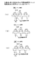
図8及び図9は、本発明の第1参考例であるソケット14を示している。ソケット14は、リードフレーム材料(例えば、銅合金)により形成されており、また図示されるように複数のソケット部材18Aにより構成されている。
【0072】
このソケット部材18Aは、前記した半導体装置12Aに形成されている外部接続端子26Aの数に対応している。具体的には、図3及び図4に示した半導体装置12は、片面12個の外部接続端子26Aを有しているため、ソケット部材18Aも12個並設された構成とされている。
ソケット部材18Aは、大略すると接続部44A,連結部50,及び実装端子部52A等を一体的に形成した構成とされている。接続部44Aは第1のコンタクト46A及び第2のコンタクト48Aにより構成されており、この第1及び第2のコンタクト46A,48Aは協働して側面から見て略C字形状をなすよう形成されている。
【0073】
また、第1及び第2のコンタクト46A,48Aの先端部には接点部54A,56Aが形成されており、この接点部54Aと接点部56Aとの間には間隙が形成されている。この間隙の寸法は、回路基板20の幅寸法より若干小さく設定されている。更に、接点部54A,56Aの位置は、半導体装置12Aに設けられた外部接続端子26Aの形成位置と対応するよう構成されている。
【0074】
よって、半導体装置12Aを接続部44Aに挿入することにより、半導体装置12Aに設けられている外部接続端子26Aは接続部44Aに保持された状態となる。この保持状態において、外部接続端子26Aは第1及び第2のコンタクト46A,48Aに挟持された状態となり、これにより外部接続端子26Aはソケット部材18Aと電気的に接続される。
【0075】
また、各接触部54A,56Aは接続部44Aの上部中央位置に形成されているため、装着状態において半導体装置12Aはソケット部材18Aに立設状態で保持される。このように、半同意装置12Aをソケット部材18A(ソケット14A)に立設させた状態で保持できることにより、半導体装置12Aの実装密度を向上させることができる。
【0076】
一方、連結部50は複数個形成された上記の接続部44Aを接続するものであり、この接続部50により各接続部44Aは電気的に接続された構成となる。また、接続部50は、ソケット14に半導体装置12Aが装着された状態において、回路基板20の面方向に対し直角方向に延在する構成となる。
また、実装端子部52Aは、連結部50の下部に下方に向け延出するよう形成されている。この実装端子部52Aは、ソケット14が配設される機器(例えばパーソナルコンピュータ)に設けられている実装基板に電気的及び機械的に接続される。これにより、ソケット14に装着された半導体装置12Aは、各ソケット部材18Aに形成されている接続部44A,連結部50,及び実装端子部52Aを介して実装基板に接続される。
【0077】
ここで、メモリとして機能する半導体装置12Aの外部接続端子18Aが有する端子特性について説明する。前記したように、半導体装置12Aに設けられる外部接続端子12Aには、電源端子(VDD),接地端子(GND),及び信号端子(SIG)が存在する。同一或いは同種の半導体装置12Aを複数個配設する場合、半導体装置12Aがメモリである場合には、同一端子特性を有する外部接続端子同志を電気的に接続することが行われる。
【0078】
即ち、図1を例に挙げて説明すれば、同図の一番手前に示される半導体装置12Aの符号26A-1で示される外部接続端子が電源端子であったとすると、残る2個の半導体装置12Aの同一位置に配設された外部接続端子は同じく電源端子となる。よって、3個配設された半導体装置12Aをソケット部材18A-1で接続することにより、1個のソケット部材18A-1で複数個の半導体装置12Aに対して電源供給を行うことができる。
【0079】
これは、接地端子(GND)及び信号端子(SIG)についても同様の構成とすることができ、よってソケット部材18Aを半導体装置12Aに設けられた外部接続端子26Aの形成位置に対応して並設することにより、複数個の半導体装置12Aを接続してモジュール化する場合、少ない配線数で半導体装置モジュール10Aを実現することができる。
【0080】
このため、本参考例にソケット14は、ソケット部材18Aを回路基板20の面方向に対し直行する方向に延在するよう構成し、ソケット14に装着される半導体装置12Aの同種の外部接続端子26Aをソケット部材18Aにより接続する構成としている。
尚、半導体装置12Aに設けられている全ての外部接続端子26Aについて、上記のようにソケット部材18Aを用いて接続することはできない。即ち、情報を書き込み或いは読み出す半導体装置を指定する指定信号が入力される外部接続端子については、共通化することができない。この外部接続端子に接続するソケット部材の構成については、説明の便宜上、後に詳述するものとする。
【0081】
上記構成とされたソケット14によれば、ソケット部材18Aを構成する複数の接続部44Aは、半導体装置12Aを装着脱自在に保持する構成であるため、ソケット14に対し高メモリ容量を有した半導体装置12Aを装着脱可能となる。このため、ソケット14を実装端子部52Aを介して実装基板(例えば、パーソナルコンピュータの実装基板)に配設した場合には、ソケット14に半導体装置12Aを装着脱することにより、パーソナルコンピュータのメモリ容量の変更を行なうことが可能となる。
【0082】
また、接続部44Aは協働して略C字形状をなす第1及び第2のコンタクト46A,48Aにより構成されているため、単に半導体装置12Aを接続部44Aで挟持することにより、ソケット部材18Aと半導体装置12Aとの電気的接続及び半導体装置12Aの保持を行なうことができる。よって、極めて簡単な構成で半導体装置12Aの接続及び保持を行なうことができる。
【0083】
また、図9に示されるように、接続部44Aの連結部50からの突出量h1はそれより下部の長さh2に比べて小さくなるよう設定されている。即ち、接続部44Aの連結部50からの突出量h1は、半導体装置12Aを保持を確実に行いうる範囲において最小の突出量となるよう構成されている。
これにより、第1及び第2のコンタクト46A,48Aの電気的抵抗の低減を図ることができ、よってコンタクト部材18Aと半導体装置12Aとの電気的接続性を向上させることができる。
【0084】
更に、上記したようにソケット部材18Aは、接続部44A,連結部50,及び実装端子部52Aを一体的に形成した構成であるため、1回のプレス加工で形成することが可能であり、よってソケット14を容易に製造することができる。ところで、上記のように接続部44Aは半導体装置12Aが装着脱(抜き差し)されるものであるため、外部接続端子26Aと接続部44Aとの間に摩擦が発生し、これを防止するためにソケット部材18Aにはパラジウムまたはニッケルメッキ(保護膜)が施されている。
【0085】
しかるに、第1及び第2のコンタクト46A,48Aに形成された接点部54A,56Aの間隙距離が狭い場合には、この接点部54A,56Aに保護膜が良好な状態でメッキできないおそれがある。これを防止するためには、接点部54A,56Aの離間距離を大きく設定すればよいが、単に接点部54A,56Aの離間距離を大きくした構成では、半導体装置12Aを挟持する保持力(バネ力)が小さくなり確実な保持が行なえないおそれがある。
【0086】
そこで、これを解決するための参考例を図10乃至図12に示す。図10乃至図12は、第2乃至第4参考例であるソケットに設けられる接続部44B〜44Dを夫々拡大して示している。
各図に示される第2乃至第4参考例に係るソケットに設けられる接続部44B〜44Dは、夫々第1のコンタクト46B〜46Dの接点部54B〜54Dと第2のコンタクト48B〜48Dの接点部56B〜56Dを、半導体装置12Aの装着方向(図中、上下方向)に対しずらして配置したことを特徴とするものである。各図において、矢印hで示すのは接点部54B〜54Dと接点部56B〜56Dのずれ量である。
【0087】
特に、図2に示される接続部44Bは接点部54B及び接点部56Bを間隙側に向け突出した構成とされており、また図3に示す接続部44Cは接点部54B及び接点部56Bが協働して略S字状の間隙を形成するよう構成したものであり、更に図12に示す接続部44Dは第1及び第2のコンタクト46D,48Dとしてピン状の部材を用い、上記参考例と異なりその側面形状をC字形状から変形させた構成のものである。
【0088】
上記のように、接点部54B〜54Dと接点部56B〜56Dを半導体装置12Aの装着方向に対してずらした構成とすることにより、装着時における半導体装置12Aを保持する力(挟持力)を大きく維持しつつ、接点部54B〜54Dと接点部56B〜56Dとの間の実質的な離間距離を大きくすることができる。即ち、各接続部44B〜44Dを平面視した場合(即ち、図中矢印Aで示す方向に見た場合)、接点部54B〜54Dと接点部56B〜56Dとは重なった状態に見える。即ち、半導体装置12Aを挟持する点からいえば、接点部54B〜54Dと接点部56B〜56Dとの離間距離は狭くなっており、よって半導体装置12Aを保持する力を大きく維持することができる。
【0089】
また、各接続部44B〜44Dを側面視した場合、図10乃至図12に示されるように、接点部54B〜54Dと接点部56B〜56Dとの離間距離は広くなっている。よって、各接点部54B〜54D,56B〜56Dに対して確実にメッキ処理を行なうことができ、外部接続端子12Aに対する耐摩擦性を向上させることができる。
【0090】
また、接点部54B〜54Dと接点部56B〜56Dとの離間距離が広いと、ソケット部材をプレス加工する際に用いる金型の形成を容易とすることができ、金型コストの低減及び第1及び第2のコンタクト46B〜46D,48B〜48Dの形成、即ちソケット部材の形成を容易に行なうことが可能となる。
一方、図8乃至図12に示したソケットでは、接続部44A〜44Dによる半導体装置12Aの保持は、第1及び第2のコンタクト46A〜46D,48A〜48Dが外部接続端子26Aを挟持することによりのみ行なわれていた。即ち、図8乃至図12に示したソケットでは、半導体装置12Aを一点においてのみ保持する構成であった。このため、装着状態において、半導体装置12Aに倒れが発生するおそれがある。
【0091】
そこで、これを解決するための参考例を図13乃至図15に示す。図13乃至図15は、第5乃至第7参考例であるソケットに設けられる接続部44E〜44Gを夫々拡大して示している。
図13は、第5参考例に係るソケットに設けられる接続部44Eを示している。本参考例に係る接続部44Eは、第1のコンタクト46Aと第2のコンタクト48Aとの間位置に、半導体装置12Aが嵌挿される係止凹部58を形成したことを特徴とするものである。
【0092】
この構成とすることにより、装着状態において半導体装置12Aは第1及び第2のコンタクト46A,48Aによる保持と共に、半導体装置12Aが係止凹部58と係合する係合力によっても保持される。このため、半導体装置12Aの保持をより確実に行なうことができる。
図14は、第6参考例に係るソケットに設けられる接続部44Fを示している。本参考例に係る接続部44Fは、前記した図13に示される接続部44Eの構成に加え、係止凹部58に対する半導体装置12Aの嵌挿を案内する案内部60を設けたことを特徴とするものである。
【0093】
この案内部60は係止凹部58と連続して形成され、上方に向かい開口した構成とされている。よって、案内部60を設けることにより、半導体装置12Aの係止凹部58への係合を容易かつ確実に行なうことができる。
図15は、第7参考例に係るソケットに設けられる接続部44Gを示している。本参考例に係る接続部44Gは、第1及び第2のコンタクト46E,48Eに夫々複数個の接点部54E,54F,56E,56Fを設けたことを特徴とするものである。
【0094】
この各接点部54E,54F,56E,56Fは、夫々半導体装置12Aの外部接続端子26Aと接触する構成とされている。また、第1のコンタクト46Eに設けられる接点部54E,54Fは図中上下方向に所定距離離間して形成され、同様に第2のコンタクト48Eに設けられる接点部56E,56Fも図中上下方向に所定距離離間して形成されている。
【0095】
接続部44Gを上記構成とすることにより、装着状態において半導体装置12Aは接続部44Gに複数の位置で保持及び電気的接続が行なわれることとなる。これにより、装着時における半導体装置12Aの保持を確実に行なうことができると共に、半導体装置12Aとソケットとの電気的接続性を向上させることができる。尚、図15に示す参考例では、係止凹部58も合わせて設けた構成を示している。
【0096】
続いて、図16乃至図18を用いて本発明の第8乃至第10参考例であるソケットについて説明する。第8乃至第10参考例に係るソケットは、ソケット部材18B〜18Dに設けられる実装端子部52B〜52Dに特徴を有するものである。
図16に示す第8参考例に係るソケット部材18Bは、実装端子部52Bを表面実装に対応するよう構成したものである。即ち、実装端子部52Bの連結部50からの下方延出長さは短くされており、実装基板に対して表面実装可能な構成とされている。
【0097】
また、図17に示す第9参考例に係るソケット部材18Cは、第8参考例と同様に表面実装に対応するよう構成したものであり、更に表面実装時における強度強化を図るために、連結部50の下部にサポート端子62を設けると共に実装端子部52Cを複数個に分割形成したことを特徴とするものである。
更に、図18に示す第10参考例に係るソケット部材18Dは、挿入実装に対応するよう構成したものであり、よって実装端子部52Dは連結部50から下方に向け長く延出形成されている。この実装端子部52Dは、実装時において実装基板に形成されている実装孔に挿入された上で、実装基板に接続(半田付け)される。このため、挿入処理の容易化を図るため、実装端子部52Dは下端部に向かうにつれて幅狭となるよう構成されている。
【0098】
上記のように、実装端子部52A〜52Dの形態は特に限定されるものではなく、表面実装及び挿入実装の双方に対応させることができ、よって所望する実装形態に応じて実装端子部52A〜52Dの形態を適宜選択することができる。
続いて、図19及び図20を用いて本発明の第11参考例であるソケットについて説明する。第11参考例に係るソケットでは、ソケット部材18E,18Fに形成される接続部44Aの中心位置と、実装端子部52E,52Fの中心位置とをずらして配置したことを特徴とするものである。
【0099】
図19(A)に示すソケット部材18Eは、接続部44Aの中心位置に対し、実装端子部52Eを図中右方向にピッチP2だけずらした構成とされている。また、図19(C)に示すソケット部材18Fは、接続部44Aの中心位置に対し、実装端子部52Fを図中左方向にピッチP3だけずらした構成とされている。尚、図19(B)に示すソケット部材18Aは前記した第1参考例に係るソケット14に設けられるものであり、接続部44Aの中心位置に実装端子部52Aが形成されている。
【0100】
図20は、上記構成とされた3種類のソケット部材18A,18E,18Fを、右側よりソケット部材18E,ソケット部材18A,ソケット部材18Fの順番で並設したソケット14を示している。各ソケット部材18A,18E,18Fに形成された外部接続端子部52A,52E,52Fは、前記のように夫々接続部44Aに対する形成位置が異なるよう構成されている。
【0101】
従って、ソケット部材18A,18E,18Fが並設された状態のソケット14を底面視すると、各外部接続端子部52A,52E,52Fは千鳥状の配列構造となる。これにより、実装端子部52A,52E,52Fの実質的な配設ピッチを狭ピッチ化(高密度化)することができ、よって多数の外部接続端子26Aを有する高密度化された半導体装置12Aにも対応することが可能となる。
【0102】
続いて、図21及び図22を用いて本発明の第12参考例であるソケットについて説明する。本参考例では、ソケット部材18Gを外部接続端子26Aの形成位置に対応するよう、隣接するソケット部材18G間の位置決めを行なう位置決め機構を設けたことを特徴とするものである。前記のように、ソケットは複数のソケット部材18Gを並設させることにより構成されるものである。
また、各ソケット部材18Gに形成された接続部44Aは、半導体装置12Aの外部接続端子26Aの形成位置に対応させる必要がある。このため、半導体装置12Aとソケットとの接続を確実に行なうためには、並設状態おける隣接するソケット部材18G間のピッチ(並設ピッチP4)を精度よく決める必要がある。
【0103】
そこで本参考例では、位置決め機構をソケット部材18Gに形成された位置決め突起64と、この位置決め突起64と係合する位置決め孔68を有するフレーム部材66とにより構成した。
位置決め突起64は、ソケット部材18Gの連結部50の上端に上方に向け突出するよう形成されている。この位置決め突起64は、ソケット部材18Gをプレス加工により製造する際に同時に形成される。よって、位置決め突起64をソケット部材18Gに形成するに際し、困難を伴うようなことはない。また、フレーム部材66は例えば絶縁性を有した樹脂或いは金属等により構成されており、所定の並設ピッチP4で位置決め孔68が高精度に穿設されている。
【0104】
上記構成とされた位置決め機構において、隣接するソケット部材18G間の並設ピッチP4を所定ピッチに設定するには、位置決め突起64と位置決め孔68を位置決めし、フレーム部材66を各ソケット部材18Gに装着する。これだけの簡単な作業により、各ソケット部材18Gの位置決めを行なうことができる。よって、極めて簡単な構成で、かつ簡単な位置決め処理で半導体装置12Aとソケット部材18Gとの接続性を向上させることができる。
【0105】
尚、フレーム部材66の配設位置はソケット部材18Gの端部に限定されるものではなく、位置決め突起64が形成されている位置であれば任意の位置に配設することが可能である。
続いて、図23及び図24を用いて本発明の第13参考例であるソケットについて説明する。本参考例も、隣接するソケット部材18A,18H間の位置決めを行なう位置決め機構を設けたことを特徴とするものであり、位置決め機構をソケット部材18A,18Hの一部を封止或いは圧入する位置決め樹脂70A,70Bにより構成したものである。
【0106】
図23に示す参考例では、ソケット部材18Aの連結部50を位置決め樹脂70Aにより封止することにより隣接するソケット部材18A間の位置決めを行なっている。この場合、位置決め樹脂70Aを形成するのに用いる金型には、ソケット部材18Aを所定の並設ピッチで保持するホルダ部が形成されており、このホルダ部にソケット部材18Aを保持させた状態で樹脂モールドを行なうことにより、位置決め樹脂70Aによりソケット部材18Aを所定並設ピッチで位置決めすることができる。
【0107】
また、図24に示す参考例では、ソケット部材18Hの実装端子部52Fを位置決め樹脂70Bに形成された圧入孔72(所定の並設ピッチで形成されている)に圧入することにより隣接するソケット部材18H間の位置決めを行なっている。また、実装端子部52Fには抜け止め爪74が形成されており、ソケット部材18Hが位置決め樹脂70Bから容易に抜けないよう構成されている。
【0108】
上記のように、連結部50を位置決め樹脂70Aにより封止、或いは実装端子部52Fを位置決め樹脂70Bに形成された圧入孔72に圧入することにより、ソケット部材18A,18Hは位置決め樹脂70A,70Bにより所定位置に固定され、よって半導体装置12Aとソケット部材18A,18Hとの接続性を向上させることができる。
【0109】
続いて、本発明の一実施例であるソケットの構成について図26乃至図29を用いて説明する。
前記したように、メモリとして機能する半導体装置12Aを複数個配設して半導体装置モジュール10を構成する場合、各半導体装置12Aに形成された外部接続端子26Aの内、同一或いは同種の機能を奏する外部接続端子26Aについては各半導体装置12A間で接続して用いることができる。そして、この構成とすることにより複数個の半導体装置12Aをモジュール化する場合、少ない配線数で半導体装置モジュール10Aを実現することができる。
【0110】
しかるに、半導体装置12Aに設けられている全ての外部接続端子26Aを上記のようにソケット部材18Aを用いて接続することはできない。即ち、複数個配設される半導体装置12Aにおいて、駆動させる半導体装置を指定する指定信号が入力される外部接続端子については、共通化することができない。
そこで本実施例に係るソケットでは、複数の半導体装置12Aの内、特定の半導体装置12Aの外部接続端子26Aにのみ信号を送信する必要がある場合には、特定の半導体装置12Aの外部接続端子26Aに対応する位置にのみ接続部44Aを配設し、他の半導体装置12Aに対応する位置には接続部44Aを配設しない構成としたことを特徴とするものである。以下、この構成について図26及び図27を用いて詳述する。
【0111】
図26は、本実施例に係るソケット14Aを示している。同図に示すソケット14Aは4本のソケット部材(説明の便宜上、各ソケット部材をS1〜S4で示す)から構成されており、また第1乃至第3の半導体装置(説明の便宜上、各半導体装置をL,M,Nと示す)が装着される構成とされている。また、同図においてNCと示された部位は、接続部44Aが配設されていない部位である。具体的には、ソケット部材S2の第3の半導体装置Nが装着される部位、ソケット部材S4の第2の半導体装置Mが装着される部位については、接続部44Aは配設されていない。
【0112】
更に、図27(A)〜(C)は、ソケット14Aに装着される3個の半導体装置L,M,Nの外部接続端子(説明の便宜上、L1〜L4,M1〜M4,N1〜N4と示す)を拡大して示している。
上記構成とされた半導体装置L,M,Nをソケット14Aに装着した場合における、接続部44Aと外部接続端子L1〜L4,M1〜M4,N1〜N4との接続状態について考察する。
【0113】
先ず、ソケット部材S1に注目する。本実施例では、第1の半導体装置Lの外部接続端子L1,第2の半導体装置Mの外部接続端子M1,及び第3の半導体装置Nの外部接続端子N1は同一の機能を有した端子とされている。このため、ソケット部材S1は、半導体装置L,M,Nが装着される全ての位置において接続部44Aが形成された構成とされている。
【0114】
これにより、半導体装置L,M,Nをソケット14Aに装着した状態において、第1の半導体装置Lの外部接続端子L1,第2の半導体装置Mの外部接続端子M1,及び第3の半導体装置Nの外部接続端子N1はソケット部材S1により電気的に接続された構成となる。
従って、1個のソケット部材S1を外部接続端子L1,M1,N1の共通した配線として用いることができる。これは、ソケット部材S3についても同様のことが言え、1個のソケット部材S3を外部接続端子L3,M3,N3の共通した配線として用いることができる。
【0115】
続いて、ソケット部材S2に注目する。本実施例では、第1の半導体装置Lの外部接続端子L2及び第2の半導体装置Mの外部接続端子M2は同一の機能を有した端子とされているが、第3の半導体装置Nの外部接続端子N3は外部接続端子L2,M2とは異なる機能を有した端子とされている。
このため、ソケット部材S2は、外部接続端子L2,M2と対応する位置については接続部44Aが形成されているが、外部接続端子N3と対応する位置については接続部44Aが形成されていない。従って、半導体装置L,M,Nをソケット14Aに装着した場合、外部接続端子N3についてはソケット部材S2から信号が供給されることはない。
【0116】
更に、ソケット部材S4に注目する。本実施例では、第1の半導体装置Lの外部接続端子L4及び第3の半導体装置Nの外部接続端子N4は同一の機能を有した端子とされているが、第2の半導体装置Mの外部接続端子M4は外部接続端子L4,N4とは異なる機能を有した端子とされている。
このため、ソケット部材S4は、外部接続端子L4,N4と対応する位置については接続部44Aが形成されているが、外部接続端子M4と対応する位置については接続部44Aが形成されていない。従って、半導体装置L,M,Nをソケット14Aに装着した場合、外部接続端子M4についてはソケット部材S4から信号が供給されることはない。
【0117】
上記構成とすることにより、半導体装置L,M,Nの外部接続端子L1〜L4,M1〜M4,N1〜N4に選択的に信号を送信することが可能となる。また、信号の供給を行ないたくない外部接続端子M4,N2については、この外部接続端子M4,N2の装着位置に対応する部位の接続端子44Aを切断して除去しておくのみで信号の供給停止を行なうことができる。
【0118】
図28は、本実施例であるソケット(ソケット部材)の製造方法を説明するための図である。同図はリードフレーム78を示しており、このリードフレーム78にソケット部材18A,18Jが形成された例を示している。このリードフレーム78は、板状基材をプレス加工(打ち抜き加工)を行なうことにより形成される。この際、ソケット部材18JのNCで示される部位は打ち抜かれ接続部は形成されていない。このように、接続部の除去はリードフレーム78の形成時に一括的に行なうことができる。
【0119】
また、図29に示す構成では、接続部44Aと連結部50とが接続する部位に幅細部80Aを形成すると共に、連結部50の接続部44Aが隣接する間位置にも幅細部80Bを形成したものである。この構成では、幅細部80Bの強度は弱いため、この幅細部80Bを図中破線X1で示す位置で切断することにより接続部44Aをソケット部材18Kから除去することができる。
【0120】
また、上記した実施例では、信号の供給を行ないたくない外部接続端子M4,N2について信号の供給を停止する手段として接続部44Aを除去する方法を説明したが、連結部50を切断することによっても同様の信号の供給停止を行なうことができる。
この場合には、幅細部80Aを図29に破線Y1,Y2で示す位置で切断すればよい。このように、幅細部80A,80Bを適宜切断することにより所望の信号供給ラインを形成することができ、よって特定の半導体装置の外部接続端子にのみ信号を送信することが可能となる。
【0121】
続いて、本発明の第15参考例であるソケットの構成について図30を用いて説明する。
本参考例に係るソケットでは、これに用いられるソケット18Lの接続部44Fが半導体装置12Aを斜めに傾けて装着できるよう構成したことを特徴とするものである。具体的には、第1のコンタクト46Fの長さを第2のコンタクト48Fの長さよりも長くすることにより、各コンタクト46F,48F間に形成される間隙が側部に位置するよう構成されている。
【0122】
この構成とすることにより、半導体装置12Aは接続部44Fに対して斜めに装着されることとなり、よって半導体装置12Aは接続部44Fに斜めに傾いた状態で保持される。これにより、装着状態における半導体装置12Aの高さを低くすることができ、よって低背化が要求されている機器に適用することが可能となる。
【0123】
図31は、第15参考例であるソケットを用いた半導体装置モジュール10Bを示している。同図に示されるように、ソケットを構成する各ソケット部材18Lは矩形状とされたソケット枠82の底部に配設されており、各半導体装置12Cはソケット部材18Lに対し斜めに装着され構成とされている。
また、各半導体装置12Cに設けられた放熱部材34には回路基板20より延出する延出部40が形成されている。更に、ソケット枠82の上部には放熱板84が形成されており、この放熱板84には延出部40と係合する係合部(図示せず)が形成されている。
【0124】
上記構成とされた半導体装置モジュール10Bは、各半導体装置12Cが傾いた状態で装着されているため、全体の形状を低背化することができる。また、延出部40が放熱板84に係合することにより熱的に接続されるため、放熱面積は増大して半導体チップ22の放熱効率を更に向上させることができる。
尚、上記した各参考例では、隣接して配置されたソケット部材18A〜18Lの間には何も配設しないか、或いは位置決めのための位置決め樹脂70A,70Bを配設するのみであった。しかるに、図32に示すように、隣接するソケット部材(図ではソケット部材18Aを例に挙げている)の間に、リード板86を配設した構成としてもよい。
【0125】
このリード板86は、例えばグランド配線(GND),電源配線(VDD)として機能するものであり、絶縁性接着剤を用いて各ソケット部材18Aに接着固定される。このように、隣接するソケット部材18Aの間に配線として機能するリード板86を配設することにより、電送系(GND,VDD)の強化を図ることができる。
【0126】
続いて、本発明の第17参考例であるソケットの構成について図33を用いて説明する。
本参考例に係るソケットに用いられるソケット部材18Mは、コンタクトピン部90Aが外部接続端子26Aの片側にのみ当接するよう構成されている。また、前記した各参考例と同様に、各コンタクトピン部90Aは連結部50により電気的,機械的に接続された構成とされている。また本参考例では、半導体装置12Aを装着保持するために、ハウジング92を設けたことを特徴としている。
【0127】
ハウジング92は絶縁性樹脂等により形成されており、例えば実装基板16に固定されている。また、ハウジング92の導体装置12Aが装着される所定位置は挿入孔94が形成されており、よって半導体装置12Aは挿入孔94に挿入されることによりハウジング92に立設状態で保持される。また、ハウジング92には収納凹部96が形成されており、コンタクトピン部90Aはこの収納凹部96内に変位可能な構成で収納されている。
【0128】
ソケット部材18Mは実装基板16上に複数個並設されることによりソケットを構成するものであり、連結部50の上部に上記したコンタクトピン部90Aが一体的に形成されると共に、連結部50の下部には実装基板16に接続される挿入実装タイプの実装端子部52Gが形成されている。このソケット部材18Mに形成されたコンタクトピン部90Aは、半導体装置12Aが装着されない状態において図中破線で示す部位に位置している。
【0129】
そして、半導体装置12Aがハウジング92の挿入孔94に装着されることにより、有するバネ性により変位し、バネ力をもって半導体装置12Aの外部接続端子26A(同図では、図示を省略している)に圧接する。これにより、コンタクトピン部90Aは半導体装置12Aと電気的に接続された状態となる。また、半導体装置12Aをハウジング92から抜き出すことにより、コンタクトピン部90Aは弾性復元力により破線で示す位置に復帰する。
【0130】
本参考例では、ハウジング92が複数個の半導体装置12Aを立設状態で装着する構成とされているため、半導体装置12Aの実装密度を向上させることができる。また、ハウジング92は半導体装置12Aを装着脱自在に保持する構成であるため、ソケット(ソケット部材18M)に対し高メモリ容量を有した半導体装置12Aを装着脱可能となり、半導体装置12Aの装着脱によりメモリ容量の変更を行なうことが可能となる。
【0131】
続いて、本発明の第18参考例であるソケットの構成について図34を用いて説明する。
本参考例に係るソケットに用いられるソケット部材18Nも、前記した第17参考例と同様に、コンタクトピン部90Bが外部接続端子26Aの片側にのみ当接する構成とされている。また、各コンタクトピン部90Bは連結部50により電気的,機械的に接続された構成とされている。また本実施例では、半導体装置12Aとコンタクトピン部90Bを電気的に接続するために、中間板98を設けたことを特徴としている。
【0132】
中間板98は絶縁性樹脂等により形成されており、固定された実装基板16にたいし、図中矢印X1,X2で示す方向に移動可能な構成とされている。また、中間板98のコンタクトピン部90Bの形成位置には開口部100が形成されており、各コンタクトピン部90Bはこの開口部100を介して中間板98の上部に延出している。
【0133】
ソケット部材18Nは実装基板16上に複数個並設されることによりソケットを構成するものであり、連結部50の上部に上記したコンタクトピン部90Bが一体的に形成されると共に、連結部50の下部には実装基板16に接続される挿入実装タイプの実装端子部52Gが形成されている。このソケット部材18Nに形成されたコンタクトピン部90Bは、半導体装置12Aが装着されない状態において図中実線で示す部位に位置している。
【0134】
このコンタクトピン部90Bはバネ性を有しており、図中矢印D1方向に向け弾性力を附勢する構成とされている。しかるに、コンタクトピン部90Bは中間板98に係合することにより矢印D1方向への弾性変形は規制されており、よって実線で示す位置に係止されている。
上記構成において、半導体装置12Aが図示しない保持手段により所定位置に装着保持されると、中間板98を図中矢印X1方向に移動させる。これにより、中間板98によるコンタクトピン部90Bの弾性変形の規制は解除され、よってコンタクトピン部90Bは矢印D1方向に変位する。
【0135】
また、半導体装置12Aの外部接続端子26Aは、コンタクトピン部90Bの変位軌跡上に位置するよう構成されているため、コンタクトピン部90Bは弾性力をもって外部接続端子26Aに圧接する。これにより、コンタクトピン部90Bは半導体装置12Aと電気的に接続された状態となる(図中、破線で示す状態がコンタクトピン部90Bと半導体装置12Aとが電気的に接続した状態である)。
【0136】
また、この接続状態より中間板98を矢印X2方向に移動させると、コンタクトピン部90Bは弾性力に抗して矢印D2方向に変位し、これによりコンタクトピン付90Bは半導体装置12Aから離間し電気的接続は解除される。
上記のように、本参考例の構成によれば、中間板98によりコンタクトピン部90Bは外部接続端子26Aと接続する接続位置(破線で示す位置)と、接続を解除する解除位置(実線で示す位置)との間で移動する構成となる。
【0137】
このため、接続状態においては積極的にコンタクトピン部90Bを外部接続端子26Aと接続させることができ、よってコンタクトピン部90Bと外部接続端子26Aとの電気的接続性を向上させることができる。また、接続解除時においては、コンタクトピン部90Bと外部接続端子26Aとを確実に離間させることができるため、コンタクトピン部90Bと外部接続端子26Aとの誤接続を防止することができる。
【0138】
続いて、本発明の第19参考例であるソケットの構成について図35を用いて説明する。
本参考例に係るソケットに用いられるソケット部材は、図33を用いて説明した第17参考例に係るソケット部材18Mと同一構成とされている。また、図35では実装基板16の図示は省略している。
【0139】
本参考例では、ソケット部材18Mに対し半導体装置12Aを移動させる移動板102を設けたことを特徴としている。この移動板102は、半導体装置12Aが挿入される挿入孔104と、ソケット部材18Mに設けられたコンタクトピン部90Cが収納される収納凹部106とが形成された構成とされている。また、移動板102は、図中矢印X1,X2方向に移動可能な構成とされている。
【0140】
次に、本参考例における動作について説明する。図35(A)は、移動基板102の挿入孔104に半導体装置12Aが装着された直後の状態を示している。この状態では、移動基板102は矢印X1方向に移動しており、よって半導体装置12Aはコンタクトピン部90Cから離間し、よって外部接続端子26Aとコンタクトピン部90Cは接続されていない。
【0141】
上記のように半導体装置12Aが移動基板102の挿入孔104に装着されると、続いて移動基板102を図中矢印X2方向に移動させる。この移動基板102の移動に伴い、半導体装置12Aも図中矢印X2方向に移動する。そして、所定距離移動した時点で、図35(B)に示されるように、半導体装置12Aの外部接続端子26Aはコンタクトピン部90Cに圧接する。
【0142】
これにより、外部接続端子26Aとコンタクトピン部90Cとは電気的に接続された状態となる。尚、半導体装置12Aをソケットから抜き取る場合には、上記の動作と逆の動作が行なわれる。
本参考例の構成によれば、外部接続端子26Aを設けた半導体装置12Aは、移動板102によりコンタクトピン部90Cと接続する接続位置と、接続を解除する解除位置との間で移動する構成となる。このため、接続状態においては強制的にコンタクトピン部90Cを外部接続端子26Aと接続させることができ、よってコンタクトピン部90Cと外部接続端子26Aとの電気的接続性を向上させることができる。
【0143】
また、接続解除時においては、移動板102により半導体装置12Aは解除位置に強制的に移動されるため、コンタクトピン部90Cと外部接続端子26Aとを確実に離間させることができ、コンタクトピン部90Cと外部接続端子26Aとの誤接続を防止することができる。
尚、上記のように半導体装置とソケットにより構成される半導体装置モジュールを構成するに際し、半導体装置とソケット(ソケット部材)の組み合わせは種々考えられる。即ち、前記したソケット部材18A〜18N、及び半導体装置12A〜12Dの何れを組み合わせて半導体装置モジュールを構成してもよい。この場合、何れの構成であっても、半導体装置12A〜12Dをソケット部材18A〜18Nに対して装着脱可能することにより、半導体モジュール全体としてのメモリ容量の変更を容易に行なうことができる。
【0144】
【発明の効果】
上述の如く本発明によれば、次に述べる種々の効果を実現することができる。
請求項1記載の発明によれば、半導体装置用ソケットは複数個の半導体装置を立設状態で装着する構成とされているため、半導体装置の実装密度を向上させることができる。また、ソケット部材は半導体装置に設けられた外部接続端子の形成位置に対応して並設された構成とされており、また各接続部は連結部により電気的に接続された構成とされているため、メモリとして機能する複数の半導体装置において、ソケット部材を同種の外部接続端子を接続する配線として用いることができる。また、接続部は半導体装置を装着脱自在に保持する構成であるため、半導体装置用ソケットに対し高メモリ容量を有した半導体装置を装着脱可能となり、メモリ容量の変更を容易に行なうことができる。
【0150】
また、請求項2記載の発明によれば、極めて簡単な構成で半導体装置との接続及び保持を行なうことができると共に、電気的抵抗が低減されることにより接続特性の向上を図ることもできる。また、1回のプレス加工で形成することが可能であるため、半導体装置用ソケットを容易に製造することができる。
また、請求項3記載の発明によれば、装着時における半導体装置を保持する力(挟持力)を大きく維持しつつ、各接点部の実質的な離間距離を大きくすることができるため、第1及び第2のコンタクトの形成を容易に行なうことが可能となる。
【0151】
また、請求項4記載の発明によれば、装着状態において半導体装置は第1及び第2のコンタクトによる保持と共に係止凹部との係合力によっても保持されるため、半導体装置の保持をより確実に行なうことができる。
また、請求項5記載の発明によれば、装着時における半導体装置の保持を確実に行なうことができると共に、半導体装置と半導体装置用ソケットの電気的接続性を向上させることができる。
【0152】
また、請求項6記載の発明によれば、メモリとして機能する複数の半導体装置において共通化できる外部接続端子については接続部を配設することにより、各半導体装置間で外部接続端子を電気的に接続することができる。また、複数の半導体装置の内、特定の半導体装置の外部接続端子にのみ信号を送信する必要がある場合には、特定の半導体装置の外部接続端子に対応する位置にのみ接続部を配設し、他の半導体装置に対応する位置には接続部を配設しない構成とすることが可能となり、特定の半導体装置の外部接続端子にのみ信号を送信する構成とすることができる。
【0153】
また、請求項7記載の発明によれば、連結部を半導体装置に設けられた外部接続端子の特性に応じて切断した構成としたことにより、特定の半導体装置の外部接続端子にのみ信号を送信することが可能となる。
また、請求項8または請求項9記載の発明によれば、実装端子部を実装形態に応じて適宜選択することができる。
【0154】
また、請求項10記載の発明によれば、ソケット部材を並設した状態において実装端子部の配設ピッチを狭ピッチ化することができ、高密度化された外部接続端子を有した半導体装置に対応することができる。
また、請求項11記載の発明によれば、ソケット部材の配設位置を高精度に決めることができ、よって装着される半導体装置との接続性を向上させることができる。
【0155】
また、請求項12記載の発明によれば、単に位置決め突起と位置決め孔を位置決めし、フレーム部材をソケット部材に装着するのみでソケット部材の位置決めを行なうことができるため、半導体装置とソケット部材との接続性を向上させることができる。
また、請求項13記載の発明によれば、ソケット部材は位置決め樹脂により所定位置に固定されるため、半導体装置とソケット部材との接続性を向上させることができる。
【0156】
また、請求項14記載の発明によれば、装着状態における半導体装置の高さを低くすることができるため、低背化が要求されている機器に適用することが可能となる。
【図面の簡単な説明】
【図1】本発明の第1参考例である半導体装置モジュールの斜視図である。
【図2】本発明の第1参考例である半導体装置モジュールの側面図である。
【図3】本発明の第1参考例である半導体装置のチップ搭載面を示す斜視図である。
【図4】本発明の第1参考例である半導体装置の背面を示す斜視図である。
【図5】(A)は本発明の第1参考例である半導体装置の断面図、(B)は本発明の第2参考例である半導体装置の断面図、(C)は本発明の第3参考例である半導体装置の断面図である。
【図6】本発明の第4参考例である半導体装置の外部接続端子の配設位置を拡大して示す底面図である。
【図7】外部接続端子の構成例を示す図である。
【図8】本発明の第1参考例である半導体装置用ソケットを示す斜視図である。
【図9】本発明の第1参考例である半導体装置用ソケットを示す側面図である。
【図10】本発明の第2参考例である半導体装置用ソケットの接続部を拡大して示す図である。
【図11】本発明の第3参考例である半導体装置用ソケットの接続部を拡大して示す図である。
【図12】本発明の第4参考例である半導体装置用ソケットの接続部を拡大して示す図である。
【図13】本発明の第5参考例である半導体装置用ソケットの接続部を拡大して示す図である。
【図14】本発明の第6参考例である半導体装置用ソケットの接続部を拡大して示す図である。
【図15】本発明の第7参考例である半導体装置用ソケットの接続部を拡大して示す図である。
【図16】本発明の第8参考例である半導体装置用ソケットの実装端子部を説明するための図である。
【図17】本発明の第9参考例である半導体装置用ソケットの実装端子部を説明するための図である。
【図18】本発明の第10参考例である半導体装置用ソケットの実装端子部を説明するための図である。
【図19】本発明の第11参考例である半導体装置用ソケットの実装端子部を説明するための図である(その1)。
【図20】本発明の第11参考例である半導体装置用ソケットの実装端子部を説明するための図である(その2)。
【図21】本発明の第12参考例である半導体装置用ソケットの位置決め突起を説明するための図である。
【図22】本発明の第12参考例である半導体装置用ソケットの位置決め方法を説明するための図である。
【図23】本発明の第13参考例である半導体装置用ソケットの位置決め方法を説明するための斜視図である(その1)。
【図24】本発明の第13参考例である半導体装置用ソケットの位置決め方法を説明するための断面図である(その2)。
【図25】本発明の第14参考例である半導体装置用ソケット及び半導体装置の実装方法を説明するための図である。
【図26】本発明の一実施例である半導体装置用ソケットの構成を説明するための図である。
【図27】本発明の一実施例である半導体装置用ソケットを用いた半導体装置の実装構造を説明するための図である。
【図28】本発明の一実施例である半導体装置用ソケットの製造方法を説明するための図である(その1)。
【図29】本発明の一実施例である半導体装置用ソケットの製造方法を説明するための図である(その2)。
【図30】本発明の第15参考例である半導体装置用ソケットの構成を説明するための図である。
【図31】本発明の第2参考例である半導体装置モジュールの概略構成図である。
【図32】本発明の第16参考例である半導体装置用ソケットの構成を説明するための図である。
【図33】本発明の第17参考例である半導体装置用ソケットの構成を説明するための図である。
【図34】本発明の第18参考例である半導体装置用ソケットの構成を説明するための図である。
【図35】本発明の第19参考例である半導体装置用ソケットの構成を説明するための図である。
【符号の説明】
10A,10B 半導体装置モジュール
12A〜12D 半導体装置
14,14A ソケット
16 実装基板
18A〜18N ソケット部材
20 回路基板
22 半導体チップ
24 封止樹脂
26A〜26F 外部接続端子
28 配線
30 ワイヤ
32 チップ搭載面
34 背面
36 放熱部材
38 位置決め溝
40 延出部
42 ポケット部
44A〜44F 接続部
46A〜46F 第1のコンタクト
48A〜48F 第2のコンタクト
50 連結部
52A〜52G 実装端子部
54A〜54F,56A〜56F 接点部
58 係止凹部
64 位置決め突起
66 フレーム部材
68 位置決め孔
70A,70B 位置決め樹脂
74 抜け止め爪
76 係合突起
78 リードフレーム
80A,80B 幅細部
82 ソケット枠
84 放熱板
90A〜90C コンタクトピン部
92 ハウジング
94,104 挿入孔
96,106 収納凹部
98 中間板
102 移動板[0001]
BACKGROUND OF THE INVENTION
The present inventionHalfSocket for conductor deviceToEspecially suitable for use as high-speed memory and high-speed memory moduleHalfSocket for conductor deviceToRelated.
In recent years, semiconductor devices (eg, DRAMs) used as memories have been increased in speed and capacity. Semiconductor devices such as DRAMs are used as storage devices for OA equipment such as personal computers and workstations.
[0002]
In addition, the memory capacity of the OA device tends to increase. Therefore, it is necessary for the user to increase the memory capacity according to the purpose of use of the OA device.
[0003]
[Prior art]
In general, when expanding the memory capacity of an OA device such as a personal computer or workstation, the semiconductor device module is mounted on the OA device body.Has become.
This semiconductor device module is called a DRAM module or SIMM (Single InLine Memory Module). A plurality of semiconductor devices (DRAM) are mounted on a circuit board, and an external connection terminal is provided on one side edge of the circuit board. It is set as the formed structure. Then, a desired memory capacity is realized by attaching / detaching the semiconductor device module to / from a socket provided in the OA device. Further, the memory capacity of semiconductor device modules currently on the market is mainly 16 MB and 32 MB.
[0004]
By the way, with recent improvements in semiconductor manufacturing technology, the density and speed of semiconductor chips have increased, and it has become possible to provide a memory capacity of 32 MB with a single semiconductor chip. Therefore, a semiconductor device on which a semiconductor chip having such a large capacity is mounted has a function equivalent to a conventional semiconductor device module with a single semiconductor device.
[0005]
[Problems to be solved by the invention]
Here, paying attention to the conventional mounting structure of the semiconductor device, soldering is used to mount the semiconductor device on the mounting substrate, and electrical connection and mechanical connection between the semiconductor device and the mounting substrate are collectively performed. The method was general.
In exceptional cases, a semiconductor device such as a CPU is mounted by mounting a socket on a mounting board and mounting the semiconductor device in the socket. This is because only a small number (one or two) of semiconductor devices such as CPUs are mounted in the OA device, so that the downsizing of the OA device is not hindered even with a mounting structure using a socket.
[0006]
On the other hand, since a large number of semiconductor devices functioning as memories such as DRAMs are arranged in the OA equipment, the mounting substrate is used in a mounting structure in which each semiconductor device is mounted on a mounting substrate using a socket. It will increase in size. For this reason, a semiconductor device such as a DRAM is mounted on a mounting board by soldering as described above. Further, in order to meet the demand for changing the memory capacity of OA equipment as described above, a semiconductor device module in which a plurality of semiconductor devices (DRAM) are soldered to a circuit board using the semiconductor device module described above is used as an OA. A configuration has been adopted in which a plurality of semiconductor devices are collectively mounted on an OA device by being attached to and detached from a socket in the device.
[0007]
However, as described above, when the memory capacity of the semiconductor device itself is increased and can be used equivalently to a conventional semiconductor device module, the semiconductor device is made to meet the demand for changing the memory capacity of OA equipment. A configuration that can be attached to and detached from the equipment is required.
Conventionally, however, the semiconductor device (DRAM) has a mounting structure that is fixed to the circuit board or the mounting board by soldering. Therefore, the semiconductor device cannot be attached to or detached from the circuit board or the mounting board, and thus the user's request There is a problem that the memory capacity cannot be changed according to the situation.
[0008]
In order to further increase the memory capacity, it is conceivable that a plurality of semiconductor devices each having a semiconductor chip with an increased capacity are assembled into a module.
The present invention has been made in view of the above points, and it is easy to change the memory capacity while reducing the size.HalfSocket for conductor deviceTheThe purpose is to provide.
[0009]
[Means for Solving the Problems]
The above problems can be solved by taking the following means.
The invention described in
A plurality of semiconductor devices each having an external connection terminal and functioning as a memory are mounted in a standing state, and are arranged side by side corresponding to the formation position of the external connection terminal provided in the semiconductor device. A socket for a semiconductor device constituted by a plurality of socket members,
The socket member is
A plurality of connection portions that hold the semiconductor device detachably and are electrically connected to the external connection terminals provided in each of the plurality of semiconductor devices in a mounted state;
A connecting portion for connecting the plurality of connecting portions in a width detail and electrically connecting the connecting portions;
A mounting terminal connected to the mounting substrate;
It is characterized by having composition which hasIs.
The invention according to
The socket for a semiconductor device according to
The connecting portion is configured by first and second contacts that cooperate to form a substantially C shape.
The invention according to
The socket for a semiconductor device according to
The contact portions of the first and second contacts that contact the external connection terminals are shifted in the mounting direction of the semiconductor device between the contact portions of the first contact and the contact portions of the second contact. It is characterized by this.
The invention according to claim 4
The socket for a semiconductor device according to
A locking recess into which the semiconductor device is inserted is formed at a position between the first and second contacts.
The invention according to
The socket for a semiconductor device according to
A plurality of contact portions that contact the external connection terminals of the first and second contacts are formed in each of the contacts.
Further, the invention described in claim 6
The connection portion is selectively disposed in accordance with characteristics of an external connection terminal provided in the semiconductor device.
The invention according to claim 7
The connecting portion is configured to be cut according to characteristics of an external connection terminal provided in the semiconductor device.
The invention according to claim 8
The mounting terminal portion has a configuration corresponding to surface mounting.
The invention according to claim 9
The mounting terminal portion has a configuration corresponding to insertion mounting.
The invention according to claim 10
The center position of the connection part and the center position of the mounting terminal part are arranged to be shifted.
The invention according to claim 11
A positioning mechanism for positioning the socket member at a position where the external connection terminal provided in the semiconductor device is formed is provided.
The invention according to claim 12
The socket for a semiconductor device according to
The positioning mechanism is
A positioning protrusion formed on the socket member;
A frame member having a positioning hole engaged with the positioning protrusion;
It is characterized by comprising.
The invention as set forth in claim 13
The socket for a semiconductor device according to
The positioning mechanism is
It is comprised by positioning resin which seals a part of said socket member.
The invention as set forth in claim 14
The connection portion is configured to mount the semiconductor device at an angle.
Further, the invention of claim 15 is
The connecting portion has a configuration in which a narrow detail narrower than the connecting portion is formed.
[0032]
The above means operates as follows.
Claim 1According to the described invention, since the semiconductor device socket is configured to mount a plurality of semiconductor devices in an upright state, the mounting density of the semiconductor devices can be improved. Moreover, the socket member which comprises the socket for semiconductor devices is set as the structure arranged in parallel corresponding to the formation position of the external connection terminal provided in the semiconductor device. For this reason, in a plurality of semiconductor devices functioning as a memory, a socket member can be used as a wiring for connecting the same type of external connection terminals.
[0033]
In addition, since the plurality of connecting portions constituting the socket member are configured to hold the semiconductor device in a detachable manner, a semiconductor device having a high memory capacity can be attached to and detached from the semiconductor device socket. For this reason, when the socket for a semiconductor device is disposed on a mounting substrate (for example, a mounting substrate for an OA device) via a mounting terminal portion, the semiconductor device is attached to and detached from the socket for a semiconductor device, so that the OA device It is possible to change the memory capacity.
[0034]
Moreover, since each connection part connected with an external connection terminal is set as the structure electrically connected by the connection part, the same kind of external connection terminal arrange | positioned in each of several semiconductor devices as mentioned above Can be electrically connected by a socket member.
Also,Claim 2According to the described invention, since the connection portion is configured by the first and second contacts that form a substantially C shape in cooperation with each other, by sandwiching the semiconductor device between the first and second contacts, Electrical connection with the semiconductor device and holding of the semiconductor device can be performed. Therefore, it is possible to connect and hold the semiconductor device with an extremely simple configuration, and to reduce the electrical resistance of the first and second contacts. Moreover, since it can be formed by one press working, the socket for a semiconductor device can be easily manufactured.
[0035]
Also,Claim 3According to the described invention,
By disposing the contact portion of the first contact and the contact portion of the second contact with respect to the mounting direction of the semiconductor device, the force (holding force) for holding the semiconductor device at the time of mounting is largely maintained, The substantial separation distance between the contact portions can be increased. As a result, the first and second contacts can be easily formed.
[0036]
Also,Claim 4According to the described invention,
By forming the locking recess into which the semiconductor device is inserted and inserted between the first and second contacts, the semiconductor device is held by the first and second contacts and is engaged with the locking recess in the mounted state. Therefore, the semiconductor device can be held more reliably.
[0037]
Also,Claim 5According to the described invention,
By forming a plurality of contact portions in contact with the external connection terminals of the first and second contacts, the semiconductor device is held and electrically connected at a plurality of positions in the mounted state. Therefore, the semiconductor device can be reliably held at the time of mounting, and the electrical connectivity between the semiconductor device and the semiconductor device socket can be improved.
[0038]
Also,Claim 6According to the described invention,
A connection portion is provided for an external connection terminal that can be shared by a plurality of semiconductor devices functioning as a memory by selectively providing a connection portion in accordance with the characteristics of the external connection terminal provided in the semiconductor device. Thus, the external connection terminals can be electrically connected between the semiconductor devices.
[0039]
In addition, when a signal needs to be transmitted only to an external connection terminal of a specific semiconductor device among a plurality of semiconductor devices, the connection portion is disposed only at a position corresponding to the external connection terminal of the specific semiconductor device. The connection portion is not provided at a position corresponding to another semiconductor device. Thereby, it becomes possible to transmit a signal only to the external connection terminal of the specific semiconductor device.
[0040]
Also,Claim 7According to the described invention,
Since the connection portion is cut according to the characteristics of the external connection terminal provided in the semiconductor device, a signal can be transmitted only to the external connection terminal of the specific semiconductor device.
For example, when a signal needs to be transmitted only to an external connection terminal of a specific semiconductor device among a plurality of semiconductor devices, the connection portion is pulled out to a position corresponding to the external connection terminal of the specific semiconductor device. Disconnect. Thereby, a signal can be transmitted only to the external connection terminal of a specific semiconductor device.
[0041]
Also,Claim 8 or Claim 9According to the described invention,
The mounting terminal portion can be appropriately selected according to the mounting form.
Also,Claim 10According to the described invention,
By disposing the center position of the connection part and the center position of the mounting terminal part, the mounting terminal part arrangement pitch is narrowed with the socket members arranged side by side.To doTherefore, it is possible to deal with a semiconductor device having external connection terminals with high density.
[0042]
Also,Claim 11According to the described invention,
By providing a positioning mechanism for positioning and juxtaposing the socket member at the position where the external connection terminal provided in the semiconductor device is provided, the arrangement position of the socket member can be determined with high accuracy, and thus the semiconductor device to be mounted Connectivity can be improved.
[0043]
Also,Claim 12According to the described invention,
Claim 11Since the positioning mechanism described above is constituted by the positioning protrusion formed on the socket member and the frame member having the positioning hole engaged with the positioning protrusion, the positioning protrusion and the positioning hole are simply positioned, and the frame member is attached to the socket. The socket member can be positioned only by mounting on the member. Therefore, the connectivity between the semiconductor device and the socket member can be improved.
[0044]
Also,Claim 13According to the described invention,
Claim 11By configuring the described positioning mechanism with a positioning resin that seals a part of the socket member, the socket member is fixed at a predetermined position by the positioning resin, so that the connectivity between the semiconductor device and the socket member is improved. Can do.
[0045]
According to the invention of claim 14,
By adopting a configuration in which the connecting portion is mounted with the semiconductor device inclined at an angle, the height of the semiconductor device in the mounted state can be reduced, so that it can be applied to equipment that requires a low profile. NaThe
[0046]
In addition, since the housing constituting the socket member is configured to hold the semiconductor device detachably, a semiconductor device having a high memory capacity can be attached to and detached from the semiconductor device socket. For this reason, when the socket for a semiconductor device is disposed on a mounting substrate (for example, a mounting substrate for an OA device) via a mounting terminal portion, the semiconductor device is attached to and detached from the socket for a semiconductor device, so that the OA device It is possible to change the memory capacity.
[0051]
DETAILED DESCRIPTION OF THE INVENTION
Next, embodiments of the present invention will be described with reference to the drawings. 1 and 2 show the present invention.First reference exampleA semiconductor module 10A is shown. In short, the semiconductor module 10A includes a
[0052]
The socket 14 is composed of a plurality of
[0053]
3, 4, and 5 (A) show the present invention.First reference
[0054]
As the
[0055]
The
[0056]
The
[0057]
The electrical connection (bonding) between the
By the way, the
[0058]
The
The external connection terminals 26 </ b> A are arranged on one side edge (lower edge portion in the figure) of the
[0059]
As described above, when the
[0060]
The
[0061]
In addition, positioning
Thus, by forming the
[0062]
As described above, the external connection terminal 26 </ b> A provided in the semiconductor device 12 </ b> A is configured to be attachable / detachable to / from the socket 14 to be mounted. For this reason,Reference exampleWith this configuration, the
[0063]
Therefore, for example, when the socket 14 is disposed in an OA device such as a personal computer, the memory capacity can be changed by attaching / detaching the
FIG. 5 (B) shows the present invention.Second reference exampleA semiconductor device 12B is shown. The semiconductor device 12B shown in the figure is shown in FIG.First reference exampleThe
[0064]
FIG. 5 (C) shows the present invention.Third reference
Thus, by forming the extending
[0065]
In addition, the formation position of the
FIG. 6 illustrates the present invention.Fourth reference exampleA semiconductor device 12D is shown. FIG. 6 is a bottom view of the semiconductor device 12D and shows a state in which the
[0066]
As shown in the figure, the
However, the position where the
[0067]
That is, the arrangement pitch of the
Each
[0068]
FIG. 7 shows another structure of the external connection terminal. As described aboveReference exampleThen, as shown in FIG. 7A, the external connection terminals 26 </ b> A are disposed on both
[0069]
In the structure shown in FIG. 7C, the
[0070]
In this structure, for example, as shown in FIGS. 25A and 25B, a socket member 18I having an engagement protrusion 76 is used, and the engagement protrusion 76 and the
[0071]
As described above, the
Next, the socket 14 will be described.
8 and 9 show the present invention.First reference exampleThe socket 14 isShow. The socket 14 is made of a lead frame material (for example, a copper alloy), and includes a plurality of
[0072]
The
In general, the
[0073]
Further,
[0074]
Therefore, by inserting the
[0075]
Further, since each of the
[0076]
On the other hand, the connecting
Further, the mounting terminal portion 52 </ b> A is formed to extend downward at the lower portion of the connecting
[0077]
Here, terminal characteristics of the
[0078]
That is, taking FIG. 1 as an example, if the external connection terminal indicated by
[0079]
The same configuration can be applied to the ground terminal (GND) and the signal terminal (SIG). Therefore, the
[0080]
For this reason,Reference exampleSocket 14
Note that all the
[0081]
According to the socket 14 having the above-described configuration, the plurality of connecting
[0082]
Further, since the connecting
[0083]
Further, as shown in FIG. 9, the protruding amount h1 of the connecting
Thereby, the electrical resistance of the first and
[0084]
Further, as described above, the
[0085]
However, when the gap distance between the
[0086]
So to solve thisReference exampleAre shown in FIGS. Figure10To FIG.Second to fourth reference examplesThe connection parts 44B-44D provided in the socket which are are each expanded and shown.
Shown in each figureSecond to fourth reference examplesThe connection portions 44B to 44D provided in the socket according to the first embodiment have contact portions 54B to 54D of the
[0087]
In particular, the connecting portion 44B shown in FIG. 2 has a configuration in which the contact portion 54B and the contact portion 56B protrude toward the gap side, and the connecting portion 44C shown in FIG. 3 cooperates with the contact portion 54B and the contact portion 56B. The connection portion 44D shown in FIG. 12 uses pin-shaped members as the first and
[0088]
As described above, by configuring the contact portions 54B to 54D and the contact portions 56B to 56D to be shifted with respect to the mounting direction of the
[0089]
Moreover, when each connection part 44B-44D is seen from the side, as FIG. 10 thru | or FIG. 12 shows, the separation distance of the contact parts 54B-54D and the contact parts 56B-56D is large. Therefore, it is possible to reliably perform the plating process on each of the contact portions 54B to 54D and 56B to 56D, and to improve the friction resistance against the
[0090]
Further, when the separation distance between the contact portions 54B to 54D and the contact portions 56B to 56D is wide, it is possible to easily form a mold used when the socket member is pressed, thereby reducing the mold cost and the first. The
On the other hand, in the socket shown in FIGS. 8 to 12, the
[0091]
So to solve thisReference exampleAre shown in FIGS. FIG. 13 to FIG.Fifth to seventh reference examplesThe connection parts 44E-44G provided in the socket which are are each expanded and shown.
FIG.5th reference exampleThe connection part 44E provided in the socket which concerns on is shown.Reference exampleThe connecting portion 44E according to the present invention is characterized in that a locking recess 58 into which the
[0092]
With this configuration, in the mounted state, the
FIG.Sixth reference
[0093]
The
FIG.Seventh reference exampleThe connection part 44G provided in the socket which concerns on is shown.Reference exampleThe connecting portion 44G is characterized in that a plurality of
[0094]
The
[0095]
By configuring the connecting portion 44G as described above, the
[0096]
Subsequently, the present invention will be described with reference to FIGS.8th to 10th reference examplesThe socket which is is demonstrated.8th to 10th reference examplesThe socket according to the above is characterized in the mounting
As shown in FIG.Eighth reference exampleThe socket member 18B according to the embodiment is configured such that the mounting
[0097]
Also shown in FIG.Ninth reference
Furthermore, as shown in FIG.10th reference exampleThe socket member 18 </ b> D according to the configuration is configured to correspond to insertion mounting, and thus the mounting terminal portion 52 </ b> D extends and extends downward from the connecting
[0098]
As described above, the form of the mounting
Subsequently, using FIG. 19 and FIG.11th reference exampleThe socket which is is demonstrated.11th reference exampleThis socket is characterized in that the center position of the connecting
[0099]
A
[0100]
FIG. 20 shows the socket 14 in which the three types of
[0101]
Accordingly, when the socket 14 in which the
[0102]
Subsequently, using FIG. 21 and FIG.12th reference exampleThe socket which is is demonstrated.Reference exampleThen, a positioning mechanism for positioning the
Further, the
[0103]
ThereforeReference exampleThe positioning mechanism is constituted by the
The
[0104]
In the positioning mechanism configured as described above, in order to set the parallel pitch P4 between the
[0105]
The arrangement position of the frame member 66 is not limited to the end portion of the
Subsequently, the present invention will be described with reference to FIGS.13th reference exampleThe socket which is is demonstrated.Reference exampleAlso, a positioning mechanism for positioning the
[0106]
As shown in FIG.Reference exampleThen, the
[0107]
Also shown in FIG.Reference exampleThen, positioning between the adjacent socket members 18H is performed by press-fitting the mounting
[0108]
As described above, the connecting
[0109]
Subsequently, the present inventionExampleThe configuration of the socket shown in Fig. 26Solstice29 will be described.
As described above, when the semiconductor device module 10 is configured by disposing a plurality of
[0110]
However, all the
Therefore, in the socket according to the present embodiment, when a signal needs to be transmitted only to the
[0111]
FIG. 26 shows the
[0112]
27A to 27C show the external connection terminals of the three semiconductor devices L, M, and N mounted in the
A connection state between the
[0113]
First, attention is paid to the socket member S1. In this embodiment, the external connection terminal L1 of the first semiconductor device L1, the external connection terminal M1 of the second semiconductor device M, and the external connection terminal N1 of the third semiconductor device N are terminals having the same function. Has been. For this reason, the socket member S1 is configured such that the
[0114]
Thereby, in a state where the semiconductor devices L, M, N are mounted in the
Accordingly, one socket member S1 can be used as a common wiring for the external connection terminals L1, M1, and N1. The same is true for the socket member S3, and one socket member S3 can be used as a common wiring for the external connection terminals L3, M3, and N3.
[0115]
Subsequently, attention is paid to the socket member S2. In this embodiment, the external connection terminal L2 of the first semiconductor device L and the external connection terminal M2 of the second semiconductor device M are terminals having the same function. The connection terminal N3 is a terminal having a function different from that of the external connection terminals L2 and M2.
For this reason, in the socket member S2, the
[0116]
Furthermore, attention is paid to the socket member S4. In this embodiment, the external connection terminal L4 of the first semiconductor device L and the external connection terminal N4 of the third semiconductor device N are terminals having the same function. The connection terminal M4 is a terminal having a function different from that of the external connection terminals L4 and N4.
For this reason, in the socket member S4, the
[0117]
With the above configuration, signals can be selectively transmitted to the external connection terminals L1 to L4, M1 to M4, and N1 to N4 of the semiconductor devices L, M, and N. For the external connection terminals M4 and N2, which do not want to supply signals, the signal supply is stopped only by cutting and removing the
[0118]
FIG. 28 is a diagram for explaining a method of manufacturing a socket (socket member) according to the present embodiment. This figure shows a lead frame 78, and shows an example in which
[0119]
In the configuration shown in FIG. 29, the
[0120]
In the above-described embodiment, the method of removing the
In this case, the
[0121]
Subsequently, the present invention15th reference exampleThe configuration of the socket will be described with reference to FIG.
Reference exampleThis socket is characterized in that the connecting
[0122]
With this configuration, the
[0123]
FIG.15th reference exampleThe semiconductor device module 10B using the socket which is is shown. As shown in the figure, each socket member 18L constituting the socket is disposed at the bottom of a rectangular socket frame 82, and each
Further, the
[0124]
Since the semiconductor device module 10B having the above-described configuration is mounted in a state in which each
In addition, the aboveReference examplesThen, nothing is disposed between the
[0125]
The
[0126]
Subsequently, the present inventionSeventeenth reference exampleThe configuration of the socket will be described with reference to FIG.
Reference
[0127]
The housing 92 is formed of an insulating resin or the like, and is fixed to the mounting
[0128]
A plurality of
[0129]
Then, when the
[0130]
Reference exampleThen, since the housing 92 is configured to mount the plurality of
[0131]
Subsequently, the present invention18th reference exampleA configuration of the socket will be described with reference to FIG.
Reference
[0132]
The intermediate plate 98 is formed of an insulating resin or the like, and is configured to be movable in the directions indicated by arrows X1 and X2 in the drawing with respect to the fixed mounting
[0133]
A plurality of
[0134]
The
In the above configuration, when the
[0135]
Further, since the
[0136]
Further, when the intermediate plate 98 is moved in the arrow X2 direction from this connected state, the
as mentioned above,Reference exampleAccording to the configuration, the
[0137]
For this reason, in the connected state, the
[0138]
Subsequently, the present invention19th reference exampleThe configuration of the socket will be described with reference to FIG.
Reference exampleThe socket member used for the socket according to FIG. 33 has been described with reference to FIG.Seventeenth reference
[0139]
Reference exampleIn this case, a moving plate 102 for moving the
[0140]
next,Reference exampleThe operation in will be described. FIG. 35A shows a state immediately after the
[0141]
When the
[0142]
As a result, the
Reference exampleAccording to the configuration, the
[0143]
Further, when the connection is released, the
Note that various combinations of the semiconductor device and the socket (socket member) are conceivable when configuring the semiconductor device module including the semiconductor device and the socket as described above. That is, the semiconductor device module may be configured by combining any of the
[0144]
【The invention's effect】
As described above, according to the present invention, various effects described below can be realized.
According to invention of
[0150]
Also,Claim 2According to the described invention, connection and holding with a semiconductor device can be performed with an extremely simple configuration, and connection characteristics can be improved by reducing electrical resistance. Moreover, since it can be formed by one press working, the socket for a semiconductor device can be easily manufactured.
Also,Claim 3According to the described invention, since the substantial separation distance between the contact portions can be increased while maintaining a large force (holding force) for holding the semiconductor device during mounting, the first and second contacts can be increased. Can be easily formed.
[0151]
Also,Claim 4According to the described invention, since the semiconductor device is held by the engaging force with the locking recess as well as the holding by the first and second contacts in the mounted state, the semiconductor device can be held more reliably.
Also,Claim 5According to the described invention, the semiconductor device can be reliably held at the time of mounting, and the electrical connectivity between the semiconductor device and the semiconductor device socket can be improved.
[0152]
Also,Claim 6According to the described invention, the external connection terminals that can be shared by a plurality of semiconductor devices functioning as a memory can be electrically connected between the semiconductor devices by disposing the connection portions. . In addition, when a signal needs to be transmitted only to an external connection terminal of a specific semiconductor device among a plurality of semiconductor devices, the connection portion is disposed only at a position corresponding to the external connection terminal of the specific semiconductor device. Thus, it is possible to adopt a configuration in which a connection portion is not provided at a position corresponding to another semiconductor device, and a configuration in which a signal is transmitted only to an external connection terminal of a specific semiconductor device.
[0153]
Also,Claim 7According to the described invention, it is possible to transmit a signal only to the external connection terminal of a specific semiconductor device by adopting a configuration in which the connecting portion is cut according to the characteristics of the external connection terminal provided in the semiconductor device. Become.
Also,Claim 8OrClaim 9According to the described invention, the mounting terminal portion can be appropriately selected according to the mounting form.
[0154]
Also,Claim 10According to the described invention, the arrangement pitch of the mounting terminal portions is narrowed in a state where the socket members are arranged side by side.To doTherefore, it is possible to deal with a semiconductor device having external connection terminals with high density.
Also,Claim 11According to the described invention, the arrangement position of the socket member can be determined with high accuracy, so that the connectivity with the semiconductor device to be mounted can be improved.
[0155]
Also,Claim 12According to the described invention, the socket member can be positioned simply by positioning the positioning protrusion and the positioning hole and mounting the frame member on the socket member, so that the connectivity between the semiconductor device and the socket member is improved. be able to.
Also,Claim 13According to the described invention, since the socket member is fixed at a predetermined position by the positioning resin, the connectivity between the semiconductor device and the socket member can be improved.
[0156]
In addition, according to the invention described in claim 14, since the height of the semiconductor device in the mounted state can be reduced, it can be applied to equipment for which a reduction in height is required.The
[Brief description of the drawings]
FIG. 1 of the present inventionFirst reference exampleIt is a perspective view of the semiconductor device module which is.
FIG. 2 of the present inventionFirst reference exampleIt is a side view of the semiconductor device module which is.
FIG. 3 of the present inventionFirst reference exampleIt is a perspective view which shows the chip | tip mounting surface of the semiconductor device which is.
FIG. 4 of the present inventionFirst reference exampleIt is a perspective view which shows the back surface of the semiconductor device which is.
FIG. 5 (A) shows the present invention.First reference exampleFIG. 4B is a cross-sectional view of the semiconductor device as shown in FIG.Second reference exampleFIG. 4C is a cross-sectional view of the semiconductor device shown in FIG.Third reference exampleIt is sectional drawing of the semiconductor device which is.
FIG. 6 shows the present invention.Fourth reference exampleIt is a bottom view which expands and shows the arrangement | positioning position of the external connection terminal of the semiconductor device which is.
FIG. 7 is a diagram illustrating a configuration example of an external connection terminal.
FIG. 8 shows the present invention.First reference exampleIt is a perspective view which shows the socket for semiconductor devices which is.
FIG. 9 shows the present invention.First reference exampleIt is a side view which shows the socket for semiconductor devices which is.
FIG. 10 shows the present invention.Second reference exampleIt is a figure which expands and shows the connection part of the socket for semiconductor devices which is.
FIG. 11 shows the present invention.Third reference exampleIt is a figure which expands and shows the connection part of the socket for semiconductor devices which is.
FIG. 12 shows the present invention.Fourth reference exampleIt is a figure which expands and shows the connection part of the socket for semiconductor devices which is.
FIG. 13 is a diagram of the present invention.5th reference exampleIt is a figure which expands and shows the connection part of the socket for semiconductor devices which is.
FIG. 14 shows the present invention.Sixth reference exampleIt is a figure which expands and shows the connection part of the socket for semiconductor devices which is.
FIG. 15 shows the present invention.Seventh reference exampleIt is a figure which expands and shows the connection part of the socket for semiconductor devices which is.
FIG. 16 shows the present invention.Eighth reference exampleIt is a figure for demonstrating the mounting terminal part of the socket for semiconductor devices which is.
FIG. 17 shows the present invention.Ninth reference exampleIt is a figure for demonstrating the mounting terminal part of the socket for semiconductor devices which is.
FIG. 18 shows the present invention.10th reference exampleIt is a figure for demonstrating the mounting terminal part of the socket for semiconductor devices which is.
FIG. 19 shows the present invention.11th reference exampleIt is a figure for demonstrating the mounting terminal part of the socket for semiconductor devices which is (the 1).
FIG. 20 shows the present invention.11th reference exampleFIG. 6 is a diagram for explaining a mounting terminal portion of the semiconductor device socket (No. 2);
FIG. 21 shows the present invention.12th reference exampleIt is a figure for demonstrating the positioning protrusion of the socket for semiconductor devices which is.
FIG. 22 shows the present invention.12th reference exampleIt is a figure for demonstrating the positioning method of the socket for semiconductor devices which is.
FIG. 23 shows the present invention.13th reference exampleFIG. 7 is a perspective view for explaining a method for positioning a socket for a semiconductor device (No. 1);
FIG. 24 shows the present invention.13th reference exampleFIG. 6 is a cross-sectional view for explaining a method for positioning a semiconductor device socket (No. 2).
FIG. 25 shows the present invention.14th reference exampleIt is a figure for demonstrating the socket for semiconductor devices which are these, and the mounting method of a semiconductor device.
FIG. 26 shows the present invention.ExampleIt is a figure for demonstrating the structure of the socket for semiconductor devices which is.
FIG. 27 shows the present invention.ExampleIt is a figure for demonstrating the mounting structure of the semiconductor device using the socket for semiconductor devices which is.
FIG. 28 shows the present invention.ExampleIt is a figure for demonstrating the manufacturing method of the socket for semiconductor devices which is (the 1).
FIG. 29 shows the present invention.ExampleFIG. 8 is a diagram for explaining a method for manufacturing the socket for a semiconductor device (No. 2).
FIG. 30 shows the present invention.15th reference exampleIt is a figure for demonstrating the structure of the socket for semiconductor devices which is.
FIG. 31 shows the present invention.Second reference exampleIt is a schematic block diagram of the semiconductor device module which is.
FIG. 32 shows the present invention.16th reference exampleIt is a figure for demonstrating the structure of the socket for semiconductor devices which is.
FIG. 33 shows the present invention.Seventeenth reference exampleIt is a figure for demonstrating the structure of the socket for semiconductor devices which is.
FIG. 34 of the present invention18th reference exampleIt is a figure for demonstrating the structure of the socket for semiconductor devices which is.
FIG. 35 shows the present invention.19th reference exampleIt is a figure for demonstrating the structure of the socket for semiconductor devices which is.
[Explanation of symbols]
10A, 10B Semiconductor device module
12A-12D semiconductor device
14,14A socket
16 Mounting board
18A-18N Socket member
20 Circuit board
22 Semiconductor chip
24 Sealing resin
26A-26F External connection terminal
28 Wiring
30 wires
32 chip mounting surface
34 Back
36 Heat dissipation member
38 Positioning groove
40 Extension
42 Pocket
44A-44F Connection
46A-46F 1st contact
48A to 48F Second contact
50 connecting part
52A to 52G mounting terminal
54A to 54F, 56A to 56F
58 Locking recess
64 Positioning protrusion
66 Frame members
68 Positioning hole
70A, 70B Positioning resin
74 Retaining claw
76 Engagement protrusion
78 Lead frame
80A, 80B width details
82 Socket frame
84 Heat sink
90A ~ 90C Contact pin part
92 Housing
94,104 Insertion hole
96,106 Storage recess
98 Intermediate plate
102 Moving plate
Claims (15)
前記ソケット部材が、
前記半導体装置を装着脱自在に保持すると共に、装着状態において複数の前記半導体装置の各々に設けられた前記外部接続端子と電気的に接続する複数の接続部と、
前記複数の接続部を幅細部で接続すると共に電気的に接続する連結部と、
実装基板に接続される実装端子部と
を有する構成としたことを特徴とする半導体装置用ソケット。A plurality of semiconductor devices each having an external connection terminal and functioning as a memory are mounted in a standing state, and are arranged side by side corresponding to the formation position of the external connection terminal provided in the semiconductor device. A socket for a semiconductor device constituted by a plurality of socket members,
The socket member is
A plurality of connection portions that hold the semiconductor device detachably and are electrically connected to the external connection terminals provided in each of the plurality of semiconductor devices in a mounted state;
A connecting portion for connecting the plurality of connecting portions in a width detail and electrically connecting the connecting portions;
A socket for a semiconductor device, comprising a mounting terminal portion connected to a mounting substrate.
前記接続部は、協働して略C字形状をなす第1及び第2のコンタクトにより構成されることを特徴とする半導体装置用ソケット。The socket for a semiconductor device according to claim 1,
The socket for a semiconductor device is characterized in that the connection portion is constituted by first and second contacts which are substantially C-shaped in cooperation.
前記第1及び第2のコンタクトの前記外部接続端子と接触する接点部を、前記第1のコンタクトの接点部と第2のコンタクトの接点部とで、前記半導体装置の装着方向にずらして配置したことを特徴とする半導体装置用ソケット。The socket for a semiconductor device according to claim 2,
The contact portions of the first and second contacts that contact the external connection terminals are shifted in the mounting direction of the semiconductor device between the contact portions of the first contact and the contact portions of the second contact. A socket for a semiconductor device.
前記第1及び第2のコンタクトの間位置に、前記半導体装置が嵌挿される係止凹部を形成したことを特徴とする半導体装置用ソケット。The socket for a semiconductor device according to claim 2 or 3,
A socket for a semiconductor device, characterized in that a locking recess into which the semiconductor device is inserted is formed at a position between the first and second contacts.
前記第1及び第2のコンタクトの前記外部接続端子と接触する接点部が、前記各コンタクトにおいて複数個形成されていることを特徴とする半導体装置用ソケット。The socket for a semiconductor device according to claim 2 or 4,
A socket for a semiconductor device, wherein a plurality of contact portions that contact the external connection terminals of the first and second contacts are formed in each of the contacts.
前記接続部を、前記半導体装置に設けられた外部接続端子の特性に応じて選択的に配設したことを特徴とする半導体装置用ソケット。The socket for a semiconductor device according to any one of claims 1 to 5,
A socket for a semiconductor device, wherein the connection portion is selectively provided in accordance with characteristics of an external connection terminal provided in the semiconductor device.
前記連結部を、前記半導体装置に設けられた外部接続端子の特性に応じて切断した構成としたことを特徴とする半導体装置用ソケット。The socket for a semiconductor device according to any one of claims 1 to 6,
A socket for a semiconductor device, wherein the connecting portion is cut in accordance with characteristics of an external connection terminal provided in the semiconductor device.
前記実装端子部は表面実装に対応した構成とされていることを特徴とする半導体装置用ソケット。The socket for a semiconductor device according to any one of claims 1 to 6,
A socket for a semiconductor device, wherein the mounting terminal portion is configured to support surface mounting.
前記実装端子部は挿入実装に対応した構成とされていることを特徴とする半導体装置用ソケット。The socket for a semiconductor device according to any one of claims 1 to 7,
The socket for a semiconductor device, wherein the mounting terminal portion is configured to be compatible with insertion mounting.
前記接続部の中心位置と前記実装端子部の中心位置とをずらして配置したことを特徴とする半導体装置用ソケット。The socket for a semiconductor device according to any one of claims 1 to 9,
A socket for a semiconductor device, wherein a center position of the connection portion and a center position of the mounting terminal portion are shifted from each other.
前記ソケット部材を前記半導体装置に設けられた前記外部接続端子の形成位置に位置決めし並設させる位置決め機構を設けたことを特徴とする半導体装置用ソケット。The socket for a semiconductor device according to any one of claims 1 to 10,
A socket for a semiconductor device, comprising a positioning mechanism for positioning the socket member at a position where the external connection terminal provided in the semiconductor device is formed.
前記位置決め機構は、
前記ソケット部材に形成された位置決め突起と、
前記位置決め突起と係合する位置決め孔を有するフレーム部材と
により構成されることを特徴とする半導体装置用ソケット。The socket for a semiconductor device according to claim 1,
The positioning mechanism is
A positioning protrusion formed on the socket member;
A socket for a semiconductor device, comprising: a frame member having a positioning hole that engages with the positioning protrusion.
前記位置決め機構は、
前記ソケット部材の一部を封止する位置決め樹脂により構成されることを特徴とする半導体装置用ソケット。The socket for a semiconductor device according to claim 1,
The positioning mechanism is
A socket for a semiconductor device comprising a positioning resin for sealing a part of the socket member.
前記接続部が、前記半導体装置を斜めに傾けて装着する構成としたことを特徴とする半導体装置用ソケット。The socket for a semiconductor device according to any one of claims 1 to 13,
A socket for a semiconductor device, wherein the connection portion is configured to attach the semiconductor device obliquely.
前記連結部に、該連結部より幅の狭い幅細部が形成された構成としたことを特徴とする半導体装置用ソケット。The socket for a semiconductor device according to any one of claims 1 to 5,
A socket for a semiconductor device, characterized in that the connecting part is formed with a narrower width detail than the connecting part.
Priority Applications (6)
| Application Number | Priority Date | Filing Date | Title |
|---|---|---|---|
| JP13685297A JP3996668B2 (en) | 1997-05-27 | 1997-05-27 | Socket for semiconductor device |
| US09/084,097 US6472744B2 (en) | 1997-05-27 | 1998-05-26 | Semiconductor module including a plurality of semiconductor devices detachably |
| TW087108131A TW417274B (en) | 1997-05-27 | 1998-05-26 | Semiconductor module including a plurality of semiconductor devices detachably |
| KR1019980019177A KR100292759B1 (en) | 1997-05-27 | 1998-05-27 | Semiconductor device, socket for semiconductor device and semiconductor device module |
| EP98304172A EP0881679A3 (en) | 1997-05-27 | 1998-05-27 | Semiconductor module including a plurality of semiconductor devices detachably |
| US10/214,306 US6696754B2 (en) | 1997-05-27 | 2002-08-08 | Semiconductor module including a plurality of semiconductor devices detachably |
Applications Claiming Priority (1)
| Application Number | Priority Date | Filing Date | Title |
|---|---|---|---|
| JP13685297A JP3996668B2 (en) | 1997-05-27 | 1997-05-27 | Socket for semiconductor device |
Publications (2)
| Publication Number | Publication Date |
|---|---|
| JPH10335546A JPH10335546A (en) | 1998-12-18 |
| JP3996668B2 true JP3996668B2 (en) | 2007-10-24 |
Family
ID=15185023
Family Applications (1)
| Application Number | Title | Priority Date | Filing Date |
|---|---|---|---|
| JP13685297A Expired - Fee Related JP3996668B2 (en) | 1997-05-27 | 1997-05-27 | Socket for semiconductor device |
Country Status (5)
| Country | Link |
|---|---|
| US (2) | US6472744B2 (en) |
| EP (1) | EP0881679A3 (en) |
| JP (1) | JP3996668B2 (en) |
| KR (1) | KR100292759B1 (en) |
| TW (1) | TW417274B (en) |
Families Citing this family (46)
| Publication number | Priority date | Publication date | Assignee | Title |
|---|---|---|---|---|
| US6089920A (en) | 1998-05-04 | 2000-07-18 | Micron Technology, Inc. | Modular die sockets with flexible interconnects for packaging bare semiconductor die |
| KR100533761B1 (en) * | 1999-04-14 | 2005-12-06 | 앰코 테크놀로지 코리아 주식회사 | semi-conduSSor package |
| JP2002117000A (en) | 2000-10-05 | 2002-04-19 | Hitachi Ltd | Memory system and connection member |
| US6992378B2 (en) * | 2000-12-30 | 2006-01-31 | Intel Corporation | Socket and package power/ground bar apparatus that increases current carrying capacity resulting in higher IC power delivery |
| JP2002204053A (en) * | 2001-01-04 | 2002-07-19 | Mitsubishi Electric Corp | Method and apparatus for mounting circuit as well as semiconductor device |
| JP2003133518A (en) * | 2001-10-29 | 2003-05-09 | Mitsubishi Electric Corp | Semiconductor module |
| JP3845408B2 (en) | 2003-10-06 | 2006-11-15 | エルピーダメモリ株式会社 | Memory module heat dissipation device |
| US7106595B2 (en) * | 2004-09-15 | 2006-09-12 | International Business Machines Corporation | Apparatus including a thermal bus on a circuit board for cooling components on a daughter card releasably attached to the circuit board |
| SG121012A1 (en) * | 2004-10-01 | 2006-04-26 | Molex Inc | Heat dissipating terminal and elctrical connector using same |
| US7310237B2 (en) * | 2004-12-10 | 2007-12-18 | Technology Advancement Group, Inc. | Device for securing a circuit board to a socket |
| JP2006324326A (en) | 2005-05-17 | 2006-11-30 | Elpida Memory Inc | Semiconductor device |
| JP2007109932A (en) * | 2005-10-14 | 2007-04-26 | Toshiba Corp | Semiconductor device |
| US7385144B2 (en) * | 2005-11-17 | 2008-06-10 | Harris Corporation | Method and apparatus for electrically connecting printed circuit boards or other panels |
| US7394149B2 (en) * | 2006-03-08 | 2008-07-01 | Microelectronics Assembly Technologies, Inc. | Thin multichip flex-module |
| US7429788B2 (en) * | 2006-03-08 | 2008-09-30 | Microelectronics Assembly Technologies, Inc. | Thin multichip flex-module |
| US7520781B2 (en) * | 2006-03-08 | 2009-04-21 | Microelectronics Assembly Technologies | Thin multichip flex-module |
| US7393226B2 (en) * | 2006-03-08 | 2008-07-01 | Microelectronics Assembly Technologies, Inc. | Thin multichip flex-module |
| TW200825931A (en) * | 2006-12-11 | 2008-06-16 | Kreton Corp | Memory packaging element and insert card module using the memory packaging element |
| WO2009110911A1 (en) * | 2008-03-07 | 2009-09-11 | Hewlett-Packard Development Company, L.P. | Combination grill and computer add-in-card retention structure |
| US8572841B2 (en) | 2008-03-19 | 2013-11-05 | Harris Corporation | Printed wiring board assembly and related methods |
| US7968989B2 (en) * | 2008-06-27 | 2011-06-28 | Integrated Device Technology, Inc | Multi-package slot array |
| US8044861B2 (en) | 2008-06-30 | 2011-10-25 | Harris Corporation | Electronic device with edge surface antenna elements and related methods |
| KR200450525Y1 (en) * | 2008-10-20 | 2010-10-08 | 엘지이노텍 주식회사 | Encoder Spacer for a Spindle Motor |
| US8278748B2 (en) * | 2010-02-17 | 2012-10-02 | Maxim Integrated Products, Inc. | Wafer-level packaged device having self-assembled resilient leads |
| US8772920B2 (en) * | 2011-07-13 | 2014-07-08 | Oracle International Corporation | Interconnection and assembly of three-dimensional chip packages |
| JP6117661B2 (en) | 2013-09-19 | 2017-04-19 | 日立オートモティブシステムズ株式会社 | Electronic control unit |
| KR102178829B1 (en) | 2013-11-20 | 2020-11-13 | 삼성전자 주식회사 | Semiconductor memory device |
| JP6604968B2 (en) * | 2014-12-18 | 2019-11-13 | 第一電子工業株式会社 | connector |
| US9871019B2 (en) | 2015-07-17 | 2018-01-16 | Invensas Corporation | Flipped die stack assemblies with leadframe interconnects |
| US9825002B2 (en) * | 2015-07-17 | 2017-11-21 | Invensas Corporation | Flipped die stack |
| US9508691B1 (en) | 2015-12-16 | 2016-11-29 | Invensas Corporation | Flipped die stacks with multiple rows of leadframe interconnects |
| US10566310B2 (en) | 2016-04-11 | 2020-02-18 | Invensas Corporation | Microelectronic packages having stacked die and wire bond interconnects |
| US9728524B1 (en) | 2016-06-30 | 2017-08-08 | Invensas Corporation | Enhanced density assembly having microelectronic packages mounted at substantial angle to board |
| US12004336B2 (en) | 2019-07-19 | 2024-06-04 | Dell Products L.P. | System and method for thermal management and electromagnetic interference management |
| US11132038B2 (en) | 2019-07-19 | 2021-09-28 | Dell Products L.P. | System and method for thermal management of shadowed devices |
| US11378608B2 (en) | 2019-07-19 | 2022-07-05 | Dell Products L.P. | System and method for device state determination |
| US11234347B2 (en) * | 2019-07-19 | 2022-01-25 | Dell Products L.P. | System and method for physical management of devices |
| US11143682B2 (en) | 2019-07-19 | 2021-10-12 | Dell Products L.P. | System and method for communicating externally from an electromagnetic interference suppressed volume |
| US10917996B1 (en) | 2019-07-19 | 2021-02-09 | Dell Products L.P. | System and method for device level thermal management and electromagnetic interference management |
| US11122718B2 (en) | 2019-07-19 | 2021-09-14 | Dell Products L.P. | System and method for device level electromagnetic interference management |
| US11644425B2 (en) | 2019-07-19 | 2023-05-09 | Dell Products L.P. | System and method for optical state determination |
| US10980159B2 (en) | 2019-07-19 | 2021-04-13 | Dell Products L.P. | System and method for managing multiple connections |
| US11129307B2 (en) | 2019-07-19 | 2021-09-21 | Dell Products L.P. | System and method for managing thermal states of devices |
| US11399450B2 (en) | 2019-07-19 | 2022-07-26 | Dell Products L.P. | System and method for managing electromagnetic interference |
| US11234350B2 (en) | 2019-08-21 | 2022-01-25 | Dell Products L.P. | System and method for isolated device access |
| US11147194B2 (en) | 2019-08-21 | 2021-10-12 | Dell Products L.P. | System and method for managing electromagnetic interference |
Family Cites Families (39)
| Publication number | Priority date | Publication date | Assignee | Title |
|---|---|---|---|---|
| US1376940A (en) | 1919-09-26 | 1921-05-03 | Ives Frederic Eugene | Color photograph or film and method of producing same |
| US3641401A (en) | 1971-03-10 | 1972-02-08 | American Lava Corp | Leadless ceramic package for integrated circuits |
| US3702464A (en) | 1971-05-04 | 1972-11-07 | Ibm | Information card |
| US3858961A (en) | 1973-06-06 | 1975-01-07 | Itt | Printed circuit board connector |
| EP0018116A1 (en) | 1979-04-13 | 1980-10-29 | Pitney Bowes, Inc. | Postal data memory |
| FR2526226A1 (en) | 1982-04-30 | 1983-11-04 | Cii Honeywell Bull | SUPPORT OF INTEGRATED CIRCUIT DEVICES |
| DE3370569D1 (en) | 1983-03-03 | 1987-04-30 | Ibm | Circuit board and connector |
| US4567545A (en) | 1983-05-18 | 1986-01-28 | Mettler Rollin W Jun | Integrated circuit module and method of making same |
| US4558912A (en) * | 1983-12-14 | 1985-12-17 | Amp Incorporated | Edge connector for chip carrier |
| US4756694A (en) * | 1986-12-19 | 1988-07-12 | Amp Incorporated | Dual row connector for low profile package |
| US4725250A (en) * | 1987-01-27 | 1988-02-16 | Amp Incorporated | High density circuit panel socket |
| US5227664A (en) | 1988-02-26 | 1993-07-13 | Hitachi, Ltd. | Semiconductor device having particular mounting arrangement |
| US4826446A (en) * | 1988-05-04 | 1989-05-02 | Burndy Corporation | Electrical contact pins and assemblies |
| US5116237A (en) * | 1988-07-11 | 1992-05-26 | Versatile Engineering Co., Inc. | Printed circuit board edge connector |
| US4992850A (en) | 1989-02-15 | 1991-02-12 | Micron Technology, Inc. | Directly bonded simm module |
| US5138434A (en) | 1991-01-22 | 1992-08-11 | Micron Technology, Inc. | Packaging for semiconductor logic devices |
| ATE132661T1 (en) | 1989-06-02 | 1996-01-15 | Whitaker Corp | PCB SOCKET WITH CLOVER LEAF CONTACT |
| US4973270A (en) * | 1989-06-02 | 1990-11-27 | Amp Incorporated | Circuit panel socket with cloverleaf contact |
| US5244403A (en) | 1991-04-10 | 1993-09-14 | Augat Inc. | Electronic component socket with external latch |
| US5254017A (en) * | 1991-09-13 | 1993-10-19 | Robinson Nugent, Inc. | Terminal for low profile edge socket |
| WO1993018559A1 (en) | 1992-03-06 | 1993-09-16 | Augat Inc. | Edge card interconnection system |
| JP2761489B2 (en) | 1992-04-06 | 1998-06-04 | モレックス インコーポレーテッド | Electrical connector |
| JP3253765B2 (en) | 1993-06-25 | 2002-02-04 | 富士通株式会社 | Semiconductor device |
| US5733136A (en) * | 1993-10-27 | 1998-03-31 | Enplas Corporation | Socket assembly |
| US5443591A (en) * | 1994-05-24 | 1995-08-22 | Tsai; Tien C. | Connector socket |
| JPH0851180A (en) | 1994-08-09 | 1996-02-20 | Hitachi Ltd | Semiconductor device |
| US5626487A (en) | 1995-02-03 | 1997-05-06 | Hon Hai Precision Ind. Co., Ltd. | Contact for slanted SIMM socket |
| US5616044A (en) * | 1995-06-06 | 1997-04-01 | Tsai; Chou-Hsuan | Zero insert-force integrated circuit socket assembly and conductive terminal pin therefor |
| US5580267A (en) * | 1995-09-19 | 1996-12-03 | Molex Incorporated | Electrical connector for a printed circuit board |
| US5746608A (en) * | 1995-11-30 | 1998-05-05 | Taylor; Attalee S. | Surface mount socket for an electronic package, and contact for use therewith |
| US5892660A (en) | 1996-08-29 | 1999-04-06 | Micron Technology, Inc. | Single in line memory module adapter |
| US6008538A (en) | 1996-10-08 | 1999-12-28 | Micron Technology, Inc. | Method and apparatus providing redundancy for fabricating highly reliable memory modules |
| KR100232221B1 (en) | 1996-12-31 | 1999-12-01 | 김영환 | Semiconductor package and method of manufacturing thereof |
| JPH11176546A (en) * | 1997-12-12 | 1999-07-02 | Otax Co Ltd | Socket for electronic component |
| US5893726A (en) | 1997-12-15 | 1999-04-13 | Micron Technology, Inc. | Semiconductor package with pre-fabricated cover and method of fabrication |
| US5966287A (en) | 1997-12-17 | 1999-10-12 | Intel Corporation | Clip on heat exchanger for a memory module and assembly method |
| US5940277A (en) | 1997-12-31 | 1999-08-17 | Micron Technology, Inc. | Semiconductor device including combed bond pad opening, assemblies and methods |
| US5990566A (en) * | 1998-05-20 | 1999-11-23 | Micron Technology, Inc. | High density semiconductor package |
| JP2000113920A (en) | 1998-10-01 | 2000-04-21 | Mitsubishi Electric Corp | Module |
-
1997
- 1997-05-27 JP JP13685297A patent/JP3996668B2/en not_active Expired - Fee Related
-
1998
- 1998-05-26 TW TW087108131A patent/TW417274B/en active
- 1998-05-26 US US09/084,097 patent/US6472744B2/en not_active Expired - Fee Related
- 1998-05-27 EP EP98304172A patent/EP0881679A3/en not_active Withdrawn
- 1998-05-27 KR KR1019980019177A patent/KR100292759B1/en not_active IP Right Cessation
-
2002
- 2002-08-08 US US10/214,306 patent/US6696754B2/en not_active Expired - Fee Related
Also Published As
| Publication number | Publication date |
|---|---|
| EP0881679A3 (en) | 2000-08-02 |
| US6696754B2 (en) | 2004-02-24 |
| KR100292759B1 (en) | 2001-09-17 |
| KR19980087400A (en) | 1998-12-05 |
| US20020000645A1 (en) | 2002-01-03 |
| JPH10335546A (en) | 1998-12-18 |
| TW417274B (en) | 2001-01-01 |
| US6472744B2 (en) | 2002-10-29 |
| US20030164544A1 (en) | 2003-09-04 |
| EP0881679A2 (en) | 1998-12-02 |
Similar Documents
| Publication | Publication Date | Title |
|---|---|---|
| JP3996668B2 (en) | Socket for semiconductor device | |
| US5541449A (en) | Semiconductor chip carrier affording a high-density external interface | |
| EP0575806B1 (en) | Package for integrated circuit chips | |
| US11515657B2 (en) | Electrical connector and method for manufacturing same | |
| TW381328B (en) | Dual substrate package assembly for being electrically coupled to a conducting member | |
| US20030155659A1 (en) | Memory module having interconnected and stacked integrated circuits | |
| CN102005433B (en) | Board with connection terminals | |
| EP1879228A1 (en) | Semiconductor package having socket function, semiconductor module, electronic circuit module, and circuit board with socket | |
| JPH0754845B2 (en) | Stepped electronic device package | |
| JPS6137795B2 (en) | ||
| JPH10189079A (en) | Connector module | |
| US6540525B1 (en) | High I/O stacked modules for integrated circuits | |
| US6917482B2 (en) | Optical module mounted body and securing method of optical module | |
| US6408509B1 (en) | Vertically mountable interposer, assembly and method | |
| KR20010070141A (en) | Electronic module | |
| KR20110098587A (en) | High-density integrated circuit module structure | |
| US6404046B1 (en) | Module of stacked integrated circuit packages including an interposer | |
| EP0449150B1 (en) | Thermal transfer plate and integrated circuit chip or other electrical component assemblies including such plate | |
| CN112180523A (en) | An 800G optical module mechanism | |
| US6590159B2 (en) | Compact stacked electronic package | |
| JPH03295266A (en) | High integrated semiconductor device | |
| JPH09199665A (en) | Mounting device | |
| CN222146225U (en) | Semiconductor package device and electronic apparatus | |
| US20070002549A1 (en) | Electronic package connected to a substrate | |
| JPS605534A (en) | Button plate integrated circuit chip connecting system |
Legal Events
| Date | Code | Title | Description |
|---|---|---|---|
| A131 | Notification of reasons for refusal |
Free format text: JAPANESE INTERMEDIATE CODE: A131 Effective date: 20061024 |
|
| A521 | Request for written amendment filed |
Free format text: JAPANESE INTERMEDIATE CODE: A523 Effective date: 20061225 |
|
| A02 | Decision of refusal |
Free format text: JAPANESE INTERMEDIATE CODE: A02 Effective date: 20070130 |
|
| A521 | Request for written amendment filed |
Free format text: JAPANESE INTERMEDIATE CODE: A523 Effective date: 20070228 |
|
| A911 | Transfer to examiner for re-examination before appeal (zenchi) |
Free format text: JAPANESE INTERMEDIATE CODE: A911 Effective date: 20070412 |
|
| A131 | Notification of reasons for refusal |
Free format text: JAPANESE INTERMEDIATE CODE: A131 Effective date: 20070522 |
|
| A521 | Request for written amendment filed |
Free format text: JAPANESE INTERMEDIATE CODE: A523 Effective date: 20070625 |
|
| TRDD | Decision of grant or rejection written | ||
| A01 | Written decision to grant a patent or to grant a registration (utility model) |
Free format text: JAPANESE INTERMEDIATE CODE: A01 Effective date: 20070731 |
|
| A61 | First payment of annual fees (during grant procedure) |
Free format text: JAPANESE INTERMEDIATE CODE: A61 Effective date: 20070803 |
|
| FPAY | Renewal fee payment (event date is renewal date of database) |
Free format text: PAYMENT UNTIL: 20100810 Year of fee payment: 3 |
|
| R150 | Certificate of patent or registration of utility model |
Free format text: JAPANESE INTERMEDIATE CODE: R150 |
|
| FPAY | Renewal fee payment (event date is renewal date of database) |
Free format text: PAYMENT UNTIL: 20100810 Year of fee payment: 3 |
|
| LAPS | Cancellation because of no payment of annual fees |