JP3992849B2 - Digital-analog converter - Google Patents
Digital-analog converter Download PDFInfo
- Publication number
- JP3992849B2 JP3992849B2 JP21853298A JP21853298A JP3992849B2 JP 3992849 B2 JP3992849 B2 JP 3992849B2 JP 21853298 A JP21853298 A JP 21853298A JP 21853298 A JP21853298 A JP 21853298A JP 3992849 B2 JP3992849 B2 JP 3992849B2
- Authority
- JP
- Japan
- Prior art keywords
- step function
- digital data
- data
- function
- digital
- Prior art date
- Legal status (The legal status is an assumption and is not a legal conclusion. Google has not performed a legal analysis and makes no representation as to the accuracy of the status listed.)
- Expired - Fee Related
Links
Images


Classifications
-
- H—ELECTRICITY
- H03—ELECTRONIC CIRCUITRY
- H03M—CODING; DECODING; CODE CONVERSION IN GENERAL
- H03M1/00—Analogue/digital conversion; Digital/analogue conversion
- H03M1/06—Continuously compensating for, or preventing, undesired influence of physical parameters
- H03M1/08—Continuously compensating for, or preventing, undesired influence of physical parameters of noise
- H03M1/0863—Continuously compensating for, or preventing, undesired influence of physical parameters of noise of switching transients, e.g. glitches
- H03M1/0872—Continuously compensating for, or preventing, undesired influence of physical parameters of noise of switching transients, e.g. glitches by disabling changes in the output during the transitions, e.g. by holding or latching
-
- H—ELECTRICITY
- H03—ELECTRONIC CIRCUITRY
- H03M—CODING; DECODING; CODE CONVERSION IN GENERAL
- H03M1/00—Analogue/digital conversion; Digital/analogue conversion
- H03M1/66—Digital/analogue converters
Landscapes
- Engineering & Computer Science (AREA)
- Theoretical Computer Science (AREA)
- Analogue/Digital Conversion (AREA)
Description
【0001】
【発明の属する技術分野】
本発明は、離散的なデジタルデータを連続的なアナログ信号に変換するデジタル−アナログ変換器に関する。なお、本明細書においては、関数の値が局所的な領域で0以外の有限の値を有し、それ以外の領域で0となる場合を「有限台」と称して説明を行うものとする。
【0002】
【従来の技術】
最近のデジタルオーディオ装置、例えばCD(コンパクトディスク)プレーヤ等においては、離散的な音楽データ(デジタルデータ)から連続的なアナログの音声信号を得るためにオーバーサンプリング技術を適用したD/A(デジタル−アナログ)変換器が用いられている。このようなD/A変換器は、入力されるデジタルデータの間を補間して擬似的にサンプリング周波数を上げるために一般にはデジタルフィルタが用いられており、各補間値をサンプルホールド回路によって保持して階段状の信号波形を生成した後にこれをローパスフィルタに通すことによって滑らかなアナログの音声信号を出力している。
【0003】
ところで、D/A変換器に含まれるデジタルフィルタによるデータ補間は、一般にはsinc関数と称される標本化関数を用いて行われる。図13は、sinc関数の説明図である。sinc関数は、ディラックのデルタ関数を逆フーリエ変換したときに現れるものであり、標本化周波数をfとしたときにsin(πft)/(πft)で定義される。このsinc関数は、t=0の標本点のみで1になり、他の全ての標本点では0となる。
【0004】
従来は、このsinc関数の波形データをFIR(finite impulse response )フィルタのタップ計数に設定したデジタルフィルタを用いることにより、オーバーサンプリングを行っている。
【0005】
【発明が解決しようとする課題】
ところで、デジタルフィルタによって離散的な音声データ間の補間演算を行うオーバーサンプリング技術を用いると、減衰特性がなだらかなローパスフィルタを用いることができるため、ローパスフィルタによる位相特性を直線位相特性に近づけるとともに標本化折返し雑音を低減することが可能になる。このような効果は擬似的なサンプリング周波数を上げれば上げるほど顕著になるが、サンプリング周波数を上げるとそれだけデジタルフィルタやサンプルホールド回路の処理速度も高速化されるため、高速化に適した高価な部品を使用する必要があり、部品コストの上昇を招く。また、画像データのように本来のサンプリング周波数自体が高い場合(例えば数MHz)には、これをオーバーサンプリングするには数十MHzから数百MHzで動作可能な部品を用いてデジタルフィルタやサンプルホールド回路を構成する必要があり、その実現が容易ではなかった。
【0006】
また、オーバーサンプリング技術を用いた場合であっても、最終的には階段状の信号波形をローパスフィルタに通して滑らかなアナログ信号を生成しているため、ローパスフィルタを用いている限り厳密な意味での直線位相特性を持たせることができなかった。また、上述したsinc関数は、±∞で0に収束する関数であるため、正確な補間値を求めようとすると、全てのデジタルデータの値を考慮する必要があるが、実際は回路規模等の都合から、考慮するデジタルデータの範囲を限定してデジタルフィルタのタップ係数の数が設定されており、得られる補間値には打ち切り誤差が含まれていた。
【0007】
このように、オーバーサンプリング技術を適用した従来のD/A変換器は、擬似的にサンプリング周波数を上げるために高速な部品が必要であって、コスト高を招いたり、あるいは実現が容易ではかった。また、ローパスフィルタを通すため位相特性の劣化があり、しかもsinc関数を適用したデジタルフィルタを用いているため打ち切り誤差が含まれ、これらに対応した出力波形の歪みが生じていた。
【0008】
本発明は、このような点に鑑みて創作されたものであり、その目的は、部品の動作速度を上げることなく歪みの少ない出力波形を得ることができるデジタル−アナログ変換器を提供することにある。
【0009】
【課題を解決するための手段】
上述した課題を解決するために、本発明のデジタル−アナログ変換器は、入力されたデジタルデータのそれぞれに対応する値を有する所定の階段関数を発生させてこれらを加算し、階段状のアナログ電圧に変換した後に複数回のアナログ積分を行うことによって、順に入力される各デジタルデータに対応する電圧をなめらかにつなぐ連続したアナログ信号を発生する。このように、順に入力される複数のデジタルデータに対応する所定の階段関数を複数のデジタルデータのそれぞれについて発生させて各階段関数の値を加算し、その後この加算結果をアナログ電圧に変換して積分することにより連続的に変化するアナログ信号が得られるため、最終的なアナログ信号を得るためにローパスフィルタを用いる必要がなく、扱う信号の周波数によって位相特性が異なるために群遅延特性が悪化するといったことがなく、歪みの少ない出力波形を得ることができる。また、オーバーサンプリングを行っていた従来の手法に比べると、部品の動作速度を上げる必要がないため、高価な部品を使用する必要がなく、部品コストの低減が可能になる。
【0010】
特に、上述した階段関数は、区分多項式によって構成された所定の標本化関数について、各区分多項式を複数回微分することにより得られる波形を用いることが好ましい。すなわち、反対にこの階段関数を複数回積分することにより、所定の標本化関数に対応した波形を得ることができるため、標本化関数による畳み込み演算を、階段関数を合成することによって等価的に実現することが可能になり、処理内容を単純化することができるため、デジタルデータをアナログ信号に変換するために必要な処理量の低減が可能になる。
【0011】
また、上述した標本化関数は、全域が1回だけ微分可能であって有限台の値を有することが好ましい。自然界に存在する各種の信号は、滑らかに変化しているため微分可能性が必要であると考えられるが、その微分可能回数は必ずしも無限回である必要はなく、むしろ1回だけ微分可能であれば充分に自然現象を近似できると考えられる。このように、有限回微分可能であって有限台な標本化関数を用いることにより数々の利点があるが、従来はこのような条件を満たす標本化関数が存在しないと考えられていた。ところが、本発明者の研究によって、上述した条件を満たす関数が見いだされた。
【0012】
具体的には、上述した標本化関数は、標本位置tが−2から+2までの間で0以外の値を有する有限台の関数であり、−2≦t<−3/2については(−t2 −4t−4)/4で、−3/2≦t<−1については(3t2 +8t+5)/4で、−1≦t<−1/2については(5t2 +12t+7)/4で、−1/2≦t<1/2については(−7t2 +4)/4で、1/2≦t<1については(5t2 −12t+7)/4で、1≦t<3/2については(3t2 −8t+5)/4で、3/2≦t≦2については(−t2 +4t−4)/4で定義されるものを用いることができる。あるいは、このような標本化関数に対応する階段関数波形としては、等間隔に配置された5つのデジタルデータに対応した所定範囲において、−1、+3、+5、−7、−7、+5、+3、−1の重み付けがなされた同じ幅の8つの区分領域からなっているものを用いることができる。また、この重み付け処理は、ビットシフトによる−2、+2、+4、−8、−8、+4、+2、−2倍の乗算処理を行った結果に対してデジタルデータ自身を加算することによって実現することが好ましい。ビットシフトによって乗算処理が行われるため、処理の簡略化、高速化が可能になる。
【0013】
このように、全域で1回だけ微分可能な標本化関数を用いることにより、複数の階段関数を加算した後に積分処理する回数を減らすことができ、処理量を低減することが可能になる。また、有限台の値を有する標本化関数を用いることにより、この有限台の区間に対応したデジタルデータのみを処理の対象とすればよいため、さらに処理量を低減することができ、しかも有限個のデジタルデータを対象に処理を行った場合の打ち切り誤差の発生を防止することができる。
【0014】
【発明の実施の形態】
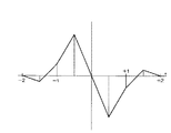
以下、本発明を適用した一実施形態のD/A変換器について、図面を参照しながら詳細に説明する。図1は、本実施形態のD/A変換器における補間演算に用いられる標本化関数の説明図である。図1に示す標本化関数H(t)は、微分可能性に着目した有限台の関数であり、例えば全域において1回だけ微分可能であって、横軸に沿った標本位置tが−2から+2の間にあるときに0以外の有限な値を有する有限台の関数である。また、H(t)は標本化関数であるため、t=0の標本位置のみで1になり、t=±1,±2の標本位置において0になるという特徴を有する。
【0015】
上述した各種の条件(標本化関数、1回だけ微分可能、有限台)を満たす関数H(t)が存在することが本発明者の研究により確かめられている。具体的には、このような標本化関数H(t)は、3階Bスプライン関数をF(t)としたときに、
H(t)=−F(t+1/2)/4+F(t)−F(t−1/2)/4…(1)
で定義することができる。ここで、3階Bスプライン関数F(t)は、
(4t2 +12t+9)/4 ;−3/2≦t<−1/2
−2t2 +3/2 ;−1/2≦t<1/2
(4t2 −12t+9)/4 ;1/2≦t<3/2 …(2)
で表される。
【0016】
上述した標本化関数H(t)は、二次の区分多項式であり、3階Bスプライン関数F(t)を用いているため、全域で1回だけの微分可能性が保証される有限台の関数となっている。また、t=±1,±2の標本位置において0となる。
【0017】
上述した(2)式を(1)式に代入して、標本化関数H(t)を区分多項式の形で求めると、
(−t2 −4t−4)/4 ;−2≦t<−3/2
(3t2 +8t+5)/4 ;−3/2≦t<−1
(5t2 +12t+7)/4 ;−1≦t<−1/2
(−7t2 +4)/4 ;−1/2≦t<1/2
(5t2 −12t+7)/4 ;1/2≦t<1
(3t2 −8t+5)/4 ;1≦t<3/2
(−t2 +4t−4)/4 ;3/2≦t≦2 …(3)
と表すことができる。
【0018】
このように、上述した関数H(t)は、標本化関数であって、全域において1回だけ微分可能であり、しかも標本位置t=±2において0に収束する有限台の関数である。したがって、この標本化関数H(t)を用いて各標本値に基づく重ね合わせを行うことにより、標本値間の値を1回だけ微分可能な関数を用いて補間することができる。
【0019】
図2は、標本値とその間の補間値との関係を示す図である。一般に、与えられた各標本値のそれぞれについて補間位置における標本化関数の値を求め、これを用いて畳み込み演算を行うことにより、各標本値の間の中間位置に対応する補間値yを求めることができる。
【0020】
従来から用いられているsinc関数はt=±∞の標本位置で0に収束する関数であるため、補間値yを正確に求めようとすると、t=±∞までの各標本値に対応して補間位置でのsinc関数の値を計算し、これを用いて畳み込み演算を行う必要があった。ところが、本実施形態で用いる標本化関数H(t)は、t=±2の標本位置で0に収束するため、補間位置を挟んで前後2個ずつの標本値を考慮すればよく、演算量を大幅に削減することができる。しかも、それ以外の標本値については、本来考慮すべきであるが演算量や精度等を考慮して無視しているというわけではなく、理論的に考慮する必要がないため、打ち切り誤差は発生しない。
【0021】
図3は、図1に示す標本化関数を用いたデータ補間の説明図である。例えば、図3(A)に示す標本位置t1における標本値Y(t1)について具体的に説明する。補間位置t0と標本位置t1との距離は、隣接する2つの標本位置間の距離を正規化して1とすると、1+aとなる。したがって、標本位置t1に標本化関数H(t)の中心位置を合わせたときの補間位置t0における標本化関数の値はH(1+a)となる。実際には、標本値Y(t1)に一致するように標本化関数H(t)の中心位置のピーク高さを合わせるため、上述したH(1+a)をY(t1)倍した値H(1+a)・Y(t1)が求めたい値となる。
【0022】
同様にして、図3(B)〜(D)に示すように、他の3つの標本値に対応して、補間位置t0における各演算結果H(a)・Y(t2)、H(1−a)・Y(t3)、H(2−a)・Y(t4)が得られる。このようにして得られた4つの演算結果H(1+a)・Y(t1)、H(a)・Y(t2)、H(1−a)・Y(t3)、H(2−a)・Y(t4)を加算して畳み込み演算を行うことにより、補間位置t0における補間値yが求められる。
【0023】
ところで、上述したように、原理的には各標本値に対応させて標本化関数H(t)の値を計算して畳み込み演算を行うことにより各標本値の間の中間位置に対応する補間値を求めることができるが、図1に示した標本化関数は全域で1回だけ微分可能な二次の区分多項式であり、この特徴を利用して、等価的な他の処理手順によって補間値を求めることができる。
【0024】
図4は、図1に示した標本化関数を1回微分した波形を示す図である。図1に示した標本化関数H(t)は、全域で1回微分可能な二次の区分多項式であるため、これを1回微分することにより、図4に示すような連続的な折れ線状の波形からなる折れ線関数を得ることができる。
【0025】
また、図5は図4に示した折れ線関数をさらに微分した波形を示す図である。但し、折れ線波形には複数の角点が含まれており、全域で微分することはできないため、隣接する2つの角点に挟まれた直線部分について微分を行うものとする。図4に示す折れ線波形を微分することにより、図5に示すような階段状の波形からなる階段関数を得ることができる。
【0026】
このように、本実施形態のD/A変換器における補間演算に用いられる標本化関数は、全域を1回微分して折れ線関数が得られ、この折れ線関数の各直線部分をさらに微分することにより階段関数が得られる。したがって、反対に図5に示した階段関数を発生させ、これを2回積分することにより、図1に示した標本化関数H(t)を得ることができる。
【0027】
なお、図5に示した階段関数は正領域と負領域とが等しい面積を有しており、これらを合計した値が0となる特徴を有している。換言すれば、このような特徴を有する階段関数を複数回積分することにより、図1に示したような全域における微分可能性が保証された有限台の標本化関数を得ることができる。
【0028】
ところで、図3に示した畳み込み演算による補間値の算出では、標本化関数H(t)の値に各標本値を乗算したが、図5に示した階段関数を2回積分して標本化関数H(t)を求める場合には、この積分処理によって得られた標本化関数の値に各標本値を乗算する場合の他に、等価的には、積分処理前の階段関数を発生させる際に、各標本値が乗算された階段関数を発生させ、この階段関数を用いて畳み込み演算を行った結果に対して2回の積分処理を行って補間値を求めることができる。本実施形態のD/A変換器は、このようにして補間値を求めており、次にその詳細を説明する。
【0029】
図6は、本実施形態のD/A変換器の構成を示す図である。同図に示すD/A変換器は、4つのデータ保持部10−1、10−2、10−3、10−4、4つの階段関数発生部11−1、11−2、11−3、11−4、加算部12、D/A変換器14、2つの積分処理部16、18、タイミング制御部20を含んで構成されている。
【0030】
各データ保持部10−1〜10−4は、所定の時間間隔で順次入力される離散的なデジタルデータを巡回的に選択して取り込み、次の取り込みタイミングが到来するまでその値を保持する。例えば、最初に入力されるデジタルデータがデータ保持部10−1に保持され、2番目に入力されるデジタルデータがデータ保持部10−2に保持される。また、3番目、4番目に入力される各デジタルデータがデータ保持部10−3、10−4に保持される。各データ保持部10−1〜10−4におけるデータの保持動作が一巡すると、次に入力される5番目のデジタルデータは、一番早くデータを保持したデータ保持部10−1に取り込まれて保持される。このようにして、順に入力される各デジタルデータがデータ保持部10−1等によって巡回的に保持される。
【0031】
各階段関数発生部11−1〜11−4は、対応するデータ保持部10−1〜10−4によるデジタルデータの保持タイミングに同期して、それぞれの保持データの値に比例した振幅(波高値)を有する階段関数を発生する。階段関数そのものは図5に示した形状を有しており、この階段関数の値が、データ保持部10−1〜10−4のそれぞれに保持されたデジタルデータの値に比例している。図5に示した階段関数の具体的な値は、上述した(3)式の各区分多項式を2回微分することにより得ることができ、以下のようになる。
【0032】
−1 ;−2≦t<−3/2
3 ;−3/2≦t<−1
5 ;−1≦t<−1/2
−7 ;−1/2≦0
−7 ;0≦t<1/2
5 ;1/2≦t<1
3 ;1≦t<3/2
−1 ;3/2≦t≦2
加算部12は、4つの階段関数発生部11−1〜11−4から出力されるそれぞれの階段関数の値をデジタル的に加算する。D/A変換器14は、加算部12から入力される階段状のデジタルデータに対応するアナログ電圧を発生する。このD/A変換器10では、入力されるデジタルデータの値に比例した一定のアナログ電圧を発生するため、入力されるデジタルデータに対応して階段状に電圧レベルが変化する出力電圧が得られる。
【0033】
縦続接続された2つの積分処理部16、18は、D/A変換器14の出力端に現れる階段状に変化する出力電圧に対して2回の積分処理を行う。前段の積分処理部16からは直線状(一次関数的)に変化する出力電圧が得られ、後段の積分処理部18からは二次関数的に変化する出力電圧が得られる。このようにして、複数のデジタルデータが一定間隔で入力されると、後段の積分処理部18からは、各デジタルデータに対応する電圧の間を1回だけ微分可能な滑らかな曲線で結んだ連続的なアナログ信号が得られる。
【0034】
ところで、上述した階段関数発生部11−1から出力される階段関数の値は、データ保持部10−1に保持されたデジタルデータの値に比例しているため、この階段関数の値に対応する電圧値に対して2つの積分処理部16、18によって積分処理を2回繰り返すことにより、後段の積分処理部18からは、図1に示した階段関数と入力されるデジタルデータとを乗算した結果に対応する電圧波形の信号が出力される。また、加算部12によって、各階段関数発生部11−1〜11−4から出力される階段関数の値を加算するということは、後段の積分処理部18から出力される信号に着目すると、図1に示した階段関数を用いて畳み込み演算を行うことに他ならない。
【0035】
したがって、本実施形態のD/A変換器にデジタルデータが一定の時間間隔で入力される場合を考えると、この入力間隔に対応させて各階段関数発生部11−1〜11−4による階段関数波形の発生開始タイミングをずらし、それぞれにおいて発生した階段関数の加算を行い、その結果をアナログ電圧に変換した後に2回の積分処理を行うことにより、一定間隔で入力されるデジタルデータに対応した電圧間を滑らかに結ぶアナログ信号が得られる。
【0036】
図7は、本実施形態のD/A変換器の動作タイミングを示す図である。図7(A)に示すように一定の時間間隔でデジタルデータD1 、D2 、D3 、…が入力されると、各データ保持部10−1〜10−4は、これらのデジタルデータD1 、D2 、D3 、…を巡回的に保持する。具体的には、データ保持部10−1は、1番目に入力されるデジタルデータD1 を取り込んで、入力されるデジタルデータが一巡するまで(5番目のデジタルデータD5 が入力されるまで)保持する(図7(B))。また、この1番目のデジタルデータD1 の保持タイミングに合わせて、階段関数発生部11−1は、このデジタルデータD1 に比例した値を有する階段関数を発生する(図7(C))。
【0037】
同様に、データ保持部10−2は、2番目に入力されるデジタルデータD2 を取り込んで、入力されるデジタルデータが一巡するまで(6番目のデジタルデータD6 が入力されるまで)保持する(図7(D))。また、この2番目のデジタルデータD2 の保持タイミングに合わせて、階段関数発生部11−2は、このデジタルデータD2 に比例した値を有する階段関数を発生する(図7(E))。
【0038】
データ保持部10−3は、3番目に入力される入力データD3 を取り込んで、入力されるデジタルデータが一巡するまで(7番目のデジタルデータD7 が入力されるまで)保持する(図7(F))。また、この3番目のデジタルデータD3 の保持タイミングに合わせて、階段関数発生部11−3は、このデジタルデータD3 に比例した値を有する階段関数を発生する(図7(G))。
【0039】
データ保持部10−4は、4番目に入力されるデジタルデータD4 を取り込んで、入力されるデジタルデータが一巡するまで(8番目のデジタルデータD8 が入力されるまで)保持する(図7(H))。また、この4番目のデジタルデータD4 の保持タイミングに合わせて、階段関数発生部11−4は、このデジタルデータD4 に比例した値を有する階段関数を発生する(図7(I))。
【0040】
加算部12は、このようにして4つの階段関数発生部11−1〜11−4のそれぞれから出力される各階段関数の値を加算する。ところで、図5に示したように、各階段関数発生部11−1〜11−4によって発生する階段関数は、図1に示した標本化関数の有限台の範囲である標本位置t=−2〜+2の領域を0.5毎に分割した8つの区分領域を有する有限台の関数である。例えば、標本位置t=−2から+2に向かって順に第1区分領域、第2区分領域、…第8区分領域とする。
【0041】
まず加算部12は、階段関数発生部11−1から出力される第7区分領域に対応する値(3D1 )と、階段関数発生部11−2から出力される第5区分領域に対応する値(−7D2 )と、階段関数発生部11−3から出力される第3区分領域に対応する値(5D3 )と、階段関数発生部11−4から出力される第1区分領域に対応する値(−D4 )とを加算して、加算結果(3D1 −7D2 +5D3 −D4 )を出力する。
【0042】
次に、加算部12は、階段関数発生部11−1から出力される第8区分領域に対応する値(−D1 )と、階段関数発生部11−2から出力される第6区分領域に対応する値(5D2 )と、階段関数発生部11−3から出力される第4区分領域に対応する値(−7D3 )と、階段関数発生部11−4から出力される第2区分領域に対応する値(3D4 )とを加算して、加算結果(−D1 +5D2 −7D3 +3D4 )を出力する。
【0043】
このようにして加算部12から順に階段状の加算結果が出力されると、D/A変換器14は、この加算結果(デジタルデータ)に基づいてアナログ電圧を発生する。このD/A変換器14では、入力されるデジタルデータの値に比例した一定のアナログ電圧が発生されるため、入力されるデジタルデータに対応して階段状に電圧レベルが変化する出力波形が得られる(図7(J))。
【0044】
D/A変換部14から階段状の電圧レベルを有する波形が出力されると、前段の積分処理部16は、この波形を積分して折れ線状の波形を出力し(図7(K))、後段の積分処理部18は、この折れ線状の波形をさらに積分して、デジタルデータD2 とD3 のそれぞれに対応した電圧値の間を1回だけ微分可能な滑らかな曲線で結ぶ出力電圧を発生する(図7(L))。
【0045】
このように、本実施形態のD/A変換器は、入力されるデジタルデータを保持するタイミングに合わせて階段関数を発生させ、この階段関数を4つのデジタルデータについて加算した後にこの加算結果に対応したアナログ電圧を発生させ、さらにその後に2回の積分処理を行うことにより、各デジタルデータに対応した電圧を滑らかにつなぐ連続したアナログ信号を発生することができる。
【0046】
特に、入力される各デジタルデータに対応させて、それぞれが異なる開始タイミングで4つの階段関数を発生させ、この加算結果に対応するアナログ電圧を発生させた後に2回の積分処理を行うことにより、連続的なアナログ信号が得られるため、従来のようにサンプルホールド回路やローパスフィルタが不要であって直線位相特性が悪化することもなく、良好な群遅延特性を実現することができる。また、標本位置tが±2において0に収束する有限台の標本化関数H(t)を用いているため、デジタルデータ間の補間処理を行うために前後4つのデジタルデータのみを用いればよく、補間演算を行うために必要な処理量を少なくすることができる。さらに、従来のようにオーバーサンプリング処理を行っていないため、入力されるデジタルデータの時間間隔に応じて決まる所定の動作速度を確保するだけでよく、特に高速な信号処理を行う必要もないため、高価な部品を用いる必要もない。
【0047】
図8は、図6に示したD/A変換器の詳細構成を示す図である。図8に示すように、各データ保持部10−1〜10−4はD型フロップフロップ(D−FF)によって構成されており、バッファ22を介して入力されるデータに対して、取り込みタイミングを入力データの1周期分ずつ順番にずらしていくことにより、入力データD1 、D2 、D3 、…を巡回的に保持する。例えば、8ビットのデジタルデータが入力されるものとすると、各データ保持部10−1〜10−4に保持された8ビットのデータは、それぞれに対応する階段関数発生部11−1〜11−4に入力される。
【0048】
図9は、階段関数発生部11−1〜11−4の詳細な構成を示す図である。なお、4つの階段関数発生部11−1〜11−4は同じ構成を有しており、以下では、代表して階段関数発生部11−1の詳細について説明する。
【0049】
図9に示すように、階段関数発生部11−1は、反転出力を有する2つのトライステートバッファ100、102と、非反転出力を有する2つのトライステートバッファ104、106と、この階段関数発生部11−1に入力されるデータとトライステートバッファ100〜106のいずれかを介して出力されるデータとを加算する加算器(ADD)108とを含んで構成されている。
【0050】
ところで、図5に示した階段関数は、横軸を上方向に+1シフトすると図10に示す階段関数に変形される。この変形後の階段関数のそれぞれの値は、2のべき乗の値になっているため、各値を乗数として入力データに対する乗算を行う場合には、単純なビットシフト操作によって乗算を実行することができる。その後、上方向に+1シフトした横軸を元に戻す処理(乗算結果に入力データを加算する処理)を行って、各階段関数発生部の出力値とすればよい。
【0051】
具体的には、トライステートバッファ100は、入力データに対して1ビット分シフトするとともに、そのシフトされたデータの各ビットを反転して出力すると同時に、加算器108のキャリー入力に1を加えることによって、(−2)倍の乗算が行われる。図10の「S1」で示すタイミングで、トライステートバッファ100から乗算結果に対応するデータを出力することにより、階段関数の第1および第8の区分領域に対応するデータが得られる。
【0052】
同様に、トライステートバッファ102は、入力データを1ビット分シフトすることにより、2倍の乗算を行う。図10の「S2」で示すタイミングで、トライステートバッファ102から乗算結果に対応するデータを出力することにより、階段関数の第2および第7の区分領域に対応するデータが得られる。
【0053】
トライステートバッファ104は、入力データを2ビット分シフトすることにより、4倍の乗算を行う。図10の「S3」で示すタイミングで、トライステートバッファ104から乗算結果に対応するデータを出力することにより、階段関数の第3および第6の区分領域に対応するデータが得られる。
【0054】
トライステートバッファ106は、入力データを3ビットシフトするとともに各ビットを反転し、加算器108のキャリー入力に1を加えることにより、(−8)倍の乗算を行う。図10の「S4」で示すタイミングで、トライステートバッファ100から乗算結果に対応するデータを出力することにより、階段関数の第4および第5の区分領域に対応するデータが得られる。
【0055】
加算器108は、トライステートバッファ100〜106のいずれかから選択的に出力される正あるいは負のデータと、階段関数発生部11−1に入力されるデータとを加算する。そして、加算器108によって得られるデータが階段関数11−1から出力される。
【0056】
なお、加算器108では、ビットシフトされた結果を反転したトライステートバッファ100、102の出力データが入力されるか、あるいはビットシフトのみがなされたトライステートバッファ104、106の出力データが入力されるかによって、処理手順の詳細が異なる。すなわち、ビットシフトがされていないデータを用いて加算を行う場合には、単純に2つのデータの加算処理が行われる。また、ビット反転が行われたデータを用いて加算を行う場合には、2つのデータを加算した後に最下位ビットb0に‘1’を加算する。加算器108に入力されたデータがいずれの種類に属するかは、最上位ビットが‘1’であるか否かを調べればよい。
【0057】
図8に示す加算器12は、2つの入力端子を有する3つの加算器(ADD)120、122、124によって構成されている。これら3つの加算器120、122、124によって、4つの階段関数発生部11−1〜11−4から出力されるそれぞれのデータが加算される。この加算結果がD/A変換器(DAC)14に入力されて階段状の電圧波形に変換され、縦続接続された2つの積分処理部16、18のうちの前段の積分処理部16に印加される。
【0058】
また、図8に示すように、前段の積分処理部16は、2つの演算増幅器140、141、2つのキャパシタ142、143、2つの抵抗144、145およびスイッチ146を含んで構成されている。一方の演算増幅器140とキャパシタ142および抵抗144によって積分回路が構成されており、抵抗144を介して演算増幅器140の反転入力端子に印加されるD/A変換器14の出力電圧に対して所定の積分動作が行われる。また、後段の積分処理部18は、2つの演算増幅器150、151、2つのキャパシタ152、153、2つの抵抗154、155およびスイッチ156を含んで構成されている。一方の演算増幅器150とキャパシタ152および抵抗154によって積分回路が構成されており、抵抗154を介して演算増幅器150の反転入力端子に印加される前段の積分処理部16の出力電圧に対して所定の積分動作が行われる。
【0059】
ところで、本実施形態のD/A変換器は、例えばテレビジョン受信機のRGB信号や輝度信号等の映像信号を得る回路として用いる用途に適している。具体的には、テレビジョン受信機用のD/A変換器は、図8に構成を示した回路をR、G、Bデータのそれぞれに対応させて3組備えており、1画面に対応するフレームを構成する各走査線毎に所定の時間間隔でそれぞれが8ビットのR、G、Bデータが入力されて、それぞれのデータを補間する連続的なR、G、Bアナログ電圧を生成する。
【0060】
実際の積分回路では、出力電圧のドリフトが生じるため、この影響を取り除く回路を有することが好ましい。本実施形態では、前段の積分処理部16に含まれる演算増幅器141とキャパシタ143および抵抗145によって平均値を0レベルに保持する回路が構成されており、演算増幅器140等によって構成される積分回路の出力の平均値が常に0Vとなるように演算増幅器140の非反転入力端子の電圧レベルが調整される。
【0061】
後段の積分処理部18に含まれる演算増幅器152とキャパシタ153および抵抗155によって平均レベル保持回路が構成されており、演算増幅器150等によって構成される積分回路の出力の平均値が、演算増幅器151の非反転入力端子に印加される電圧レベルと同じになるように、演算増幅器150の非反転入力端子の電圧レベルが調整される。なお、演算増幅器151の非反転入力端子に印加される電圧レベルは、入力データそのものをアナログ電圧に変換してその平均レベルを求めたものが用いられ、この電圧レベルを求めるために、順次入力される入力データを保持するD型フリップフロップによって構成されるデータ保持部180と、この保持されたデジタルデータに対応するアナログ電圧を発生するD/A変換器182と、D/A変換器182の出力電圧を積分する積分回路184とが備わっている。
【0062】
また、1フレーム毎に2つの積分処理部16、18に含まれる各積分回路の積分キャパシタに蓄積される電荷をリセットするために、スイッチ146、156が設けられており、垂直ブランキング信号がD型フリップフロップによって構成される同期化回路186によって同期化されて、垂直ブランキング期間に2つのスイッチ146、156がオン状態になる。このとき、演算増幅器140に接続されたキャパシタ142と演算増幅器150に接続されたキャパシタ152のそれぞれが放電され、それぞれの積分回路がリセットされる。
【0063】
図11は、タイミング制御部20の詳細な構成を示す図である。同図に示すように、タイミング制御部20は、3ビットカウンタ160と、非反転出力を有する3つの排他的論理和回路161〜163と、反転出力を有する2つの排他的論理和回路164、165と、非反転出力を有する3つの論理積回路166〜170と、反転出力を有する3つの論理和回路171〜173とを含んで構成されている。
【0064】
また、図12は、図11に示したタイミング制御部20の動作タイミングを示す図である。図12において示したCLK、b0〜b2、c1〜c5、d1〜d8のそれぞれの波形は、図11においてそれぞれの符号を付した箇所に現れる波形を示している。図11および図12に示すように、3ビットカウンタ160は、入力されるクロック信号CLKに同期したカウント動作を行っており、このクロック信号が立ち上がる毎にカウントアップされ、3ビット出力b0、b1、b2が更新される。
【0065】
上述したタイミング制御部20を用いて各階段関数発生部11−1〜11−4に含まれる3つのスイッチのオンオフ状態を切り替えることにより、図7(C)、(E)、(G)、(I)に示した各階段関数を発生させることができる。具体的には、階段関数発生部11−1によって図7(C)に示した階段関数を発生させるために、この階段関数発生部11−1内の4つのトライステートバッファ100〜106のオンオフ状態を、図11に示した論理和回路171の出力(d3)、論理積回路169の出力(d7)、論理積回路167の出力(d2)、論理積回路166の出力(d1)の論理状態によってそれぞれ切り替える。
【0066】
同様に、階段関数発生部11−2によって図7(E)に示した階段関数を発生させるために、この階段関数発生部11−2内の4つのトライステートバッファ100〜106のオンオフ状態を、図11に示した論理和回路173の出力(d6)、論理積回路170の出力(d8)、論理和回路172の出力(d5)、論理積回路168の出力(d4)の論理状態によってそれぞれ切り替える。階段関数発生部11−3によって図7(G)に示した階段関数波形を発生させるために、この階段関数発生部11−3内の4つのトライステートバッファ100〜106のオンオフ状態を、図11に示した論理積回路169の出力(d7)、論理和回路171の出力(d3)、論理積回路166の出力(d1)、論理積回路167の出力(d2)の論理状態によってそれぞれ切り替える。階段関数発生部11−4によって図7(I)に示した階段関数を発生させるために、この階段関数発生部11−4内の4つのトライステートバッファ100〜106のオンオフ状態を、図11に示した論理積回路170の出力(d8)、論理和回路173の出力(d6)、論理積回路168の出力(d4)、論理和回路172の出力(d5)の論理状態によってそれぞれ切り替える。
【0067】
なお、本発明は上記実施形態に限定されるものではなく、本発明の要旨の範囲内で種々の変形実施が可能である。例えば、上述した実施形態では、標本化関数を全域で1回だけ微分可能な有限台の関数としたが、微分可能回数を2回以上に設定してもよい。また、図1に示すように、本実施形態の標本化関数は、t=±2で0に収束するようにしたが、t=±3以上で0に収束するようにしてもよい。例えば、t=±3で0に収束するようにした場合には、図6に示したD/A変換器に含まれるデータ保持部や階段関数発生部のそれぞれの数を6とし、6個のデジタルデータを対象に補間処理を行ってこれらのデジタルデータをなめらかにつなぐアナログ電圧を発生すればよい。
【0068】
また、必ずしも有限台の標本化関数を用いて補間処理を行う場合に限らず、−∞〜+∞の範囲で値を有する有限回微分可能な標本化関数を用い、有限の標本位置に対応する複数個のデジタルデータのみを補間処理の対象とするようにしてもよい。例えば、このような標本化関数が二次の区分多項式で定義されているものとすると、各区分多項式を2回微分することにより所定の階段関数波形を得ることができるため、この階段関数波形を用いて電圧の合成を行った結果に対して2回の積分処理を行うことにより、デジタルデータに対応した電圧をなめらかにつなぐアナログ信号を得ることができる。
【0069】
また、上述した実施形態では、D/A変換器の用途の一例としてテレビジョン受像器に使用する場合を説明したが、それ以外の用途、例えばコンパクトディスク等に記録されたデジタルのオーディオデータをアナログのオーディオ音声に変換する場合などに本発明のD/A変換器を用いることができる。
【0070】
【発明の効果】
上述したように、本発明によれば、順に入力される複数のデジタルデータのそれぞれに対応する所定の階段関数を発生させてこれらを加算し、その後この加算結果をアナログ電圧に変換して積分することにより連続的に変化するアナログ電圧が得られるため、最終的なアナログ信号を得るためにローパスフィルタを用いる必要がなく、扱う信号の周波数によって位相特性が異なるために群遅延特性が悪化するといったことがなく、歪みの少ない出力波形を得ることができる。また、オーバーサンプリングを行っていた従来の手法に比べると、部品の動作速度を上げる必要がないため、高価な部品を使用する必要がなく、部品コストの低減が可能になる。
【図面の簡単な説明】
【図1】本実施形態のD/A変換器における補間演算に用いられる標本化関数の説明図である。
【図2】標本値とその間の補間値との関係を示す図である。
【図3】図1に示す標本化関数を用いたデータ補間の説明図である。
【図4】図1に示した標本化関数を1回微分した波形を示す図である。
【図5】図4に示した折れ線関数をさらに微分した波形を示す図である。
【図6】本実施形態のD/A変換器の構成を示す図である。
【図7】本実施形態のD/A変換器の動作タイミングを示す図である。
【図8】図6に示したD/A変換器の詳細構成を示す図である。
【図9】階段関数発生部の詳細構成を示す図である。
【図10】変形後の階段関数と階段関数発生部内の各トライステートバッファのオンオフ切替タイミングとの関係を示す図である。
【図11】タイミング制御部の詳細な構成を示す図である。
【図12】図11に示したタイミング制御部の動作タイミングを示す図である。
【図13】sinc関数の説明図である。
【符号の説明】
10−1、10−2、10−3、10−4 データ保持部
11−1、11−2、11−3、11−4 階段関数発生部
12 加算器
14 D/A(デジタル−アナログ)変換器
16、18 積分処理部
20 タイミング制御部[0001]
BACKGROUND OF THE INVENTION
The present invention relates to a digital-analog converter that converts discrete digital data into a continuous analog signal. In this specification, the case where the value of a function has a finite value other than 0 in a local region and becomes 0 in other regions is referred to as a “finite platform”. .
[0002]
[Prior art]
In a recent digital audio device such as a CD (compact disc) player, a D / A (digital-digital) to which an oversampling technique is applied in order to obtain a continuous analog audio signal from discrete music data (digital data). Analog) converters are used. In such D / A converters, a digital filter is generally used to interpolate between input digital data and increase the sampling frequency in a pseudo manner, and each interpolation value is held by a sample hold circuit. A smooth analog audio signal is output by generating a stepped signal waveform and passing it through a low-pass filter.
[0003]
Incidentally, data interpolation by a digital filter included in the D / A converter is generally performed using a sampling function called a sinc function. FIG. 13 is an explanatory diagram of a sinc function. The sinc function appears when the Dirac delta function is subjected to inverse Fourier transform, and is defined as sin (πft) / (πft) where the sampling frequency is f. The sinc function is 1 only at the t = 0 sample point, and is 0 at all other sample points.
[0004]
Conventionally, oversampling is performed by using a digital filter in which the waveform data of the sinc function is set to the tap count of an FIR (finite impulse response) filter.
[0005]
[Problems to be solved by the invention]
By the way, if an oversampling technique that performs interpolation between discrete audio data using a digital filter is used, a low-pass filter with a gentle attenuation characteristic can be used. It is possible to reduce the aliasing noise. Such effects become more noticeable as the pseudo sampling frequency is increased. However, the higher the sampling frequency, the faster the processing speed of the digital filter and sample hold circuit. Need to be used, leading to increased component costs. When the original sampling frequency itself is high (for example, several MHz) as in image data, a digital filter or sample hold is used to oversample this by using components that can operate at several tens to several hundreds of MHz. It is necessary to configure a circuit, and its realization is not easy.
[0006]
Even when oversampling technology is used, a smooth analog signal is finally generated by passing the stepped signal waveform through a low-pass filter, so as long as the low-pass filter is used, it has strict meaning. It was not possible to have a linear phase characteristic at. In addition, since the sinc function described above is a function that converges to 0 at ± ∞, it is necessary to consider all digital data values when trying to obtain an accurate interpolation value. Therefore, the number of tap coefficients of the digital filter is set by limiting the range of the digital data to be considered, and the obtained interpolation value includes a truncation error.
[0007]
As described above, the conventional D / A converter to which the oversampling technique is applied requires high-speed components in order to increase the sampling frequency in a pseudo manner, which causes an increase in cost or is difficult to realize. . In addition, the phase characteristic is deteriorated because it passes through the low-pass filter. Further, since the digital filter to which the sinc function is applied is used, a truncation error is included, and distortion of the output waveform corresponding to these errors occurs.
[0008]
The present invention was created in view of the above points, and an object of the present invention is to provide a digital-analog converter capable of obtaining an output waveform with less distortion without increasing the operation speed of components. is there.
[0009]
[Means for Solving the Problems]
In order to solve the above-described problem, the digital-analog converter according to the present invention generates a predetermined step function having a value corresponding to each of input digital data, adds them, and adds a step-like analog voltage. By performing analog integration a plurality of times after conversion into a continuous analog signal, a continuous analog signal that smoothly connects the voltages corresponding to each digital data input in sequence is generated. In this way, a predetermined step function corresponding to a plurality of digital data input in sequence is generated for each of the plurality of digital data, the values of the respective step functions are added, and then the addition result is converted into an analog voltage. Since an analog signal that changes continuously is obtained by integration, it is not necessary to use a low-pass filter to obtain a final analog signal, and the phase characteristics differ depending on the frequency of the signal to be handled, so that the group delay characteristics deteriorate. Thus, an output waveform with little distortion can be obtained. Further, compared to the conventional method in which oversampling is performed, it is not necessary to increase the operation speed of the components, so that it is not necessary to use expensive components, and the component cost can be reduced.
[0010]
In particular, the step function described above preferably uses a waveform obtained by differentiating each piecewise polynomial multiple times with respect to a predetermined sampling function constituted by the piecewise polynomial. In other words, by integrating this step function multiple times, a waveform corresponding to a predetermined sampling function can be obtained, so convolution operation using the sampling function is equivalently realized by synthesizing the step function. Since the processing content can be simplified, the amount of processing necessary for converting digital data into an analog signal can be reduced.
[0011]
Moreover, it is preferable that the sampling function mentioned above has the value of a finite stand so that the whole region can be differentiated only once. Various signals that exist in nature are considered to be differentiable because they change smoothly, but the number of differentiables does not necessarily have to be infinite, rather they can be differentiated only once. It is considered that natural phenomena can be approximated sufficiently. As described above, there are a number of advantages by using a sampling function that is finitely differentiable and has a finite stage. Conventionally, it has been considered that there is no sampling function that satisfies such a condition. However, a function satisfying the above-described conditions has been found by the inventors' research.
[0012]
Specifically, the sampling function described above is a function of a finite stage having a value other than 0 when the sample position t is between −2 and +2, and for −2 ≦ t <−3/2 (− t 2 −4t−4) / 4, and −3 / 2 ≦ t <−1 (3t 2 + 8t + 5) / 4, and for −1 ≦ t <−1/2, (5t 2 + 12t + 7) / 4, and for −1 / 2 ≦ t <1/2 (−7t 2 +4) / 4, and for 1/2 ≦ t <1, (5t 2 −12t + 7) / 4, and (3t for 1 ≦ t <3/2 2 −8t + 5) / 4 and for 3/2 ≦ t ≦ 2, (−t 2 Those defined by + 4t-4) / 4 can be used. Alternatively, as a step function waveform corresponding to such a sampling function, −1, +3, +5, −7, −7, +5, +3 in a predetermined range corresponding to five digital data arranged at equal intervals. , −1 weighted ones, and those composed of eight divided regions of the same width can be used. This weighting process is realized by adding the digital data itself to the result of the multiplication process of -2, +2, +4, -8, -8, +4, +2, and -2 times by bit shift. It is preferable. Since multiplication processing is performed by bit shift, the processing can be simplified and speeded up.
[0013]
Thus, by using a sampling function that can be differentiated only once over the entire area, the number of integration processes after adding a plurality of step functions can be reduced, and the amount of processing can be reduced. In addition, by using a sampling function having a finite stage value, it is only necessary to process only the digital data corresponding to the section of the finite stage, so that the processing amount can be further reduced and the finite number can be reduced. It is possible to prevent censoring errors when processing is performed on the digital data.
[0014]
DETAILED DESCRIPTION OF THE INVENTION
Hereinafter, a D / A converter according to an embodiment to which the present invention is applied will be described in detail with reference to the drawings. FIG. 1 is an explanatory diagram of a sampling function used for interpolation calculation in the D / A converter of this embodiment. The sampling function H (t) shown in FIG. 1 is a finite function that focuses on differentiability. For example, the sampling function H (t) can be differentiated only once in the entire region, and the sample position t along the horizontal axis is -2. It is a function of a finite stage having a finite value other than 0 when it is between +2. Further, since H (t) is a sampling function, it has a feature that it becomes 1 only at the sample position at t = 0 and becomes 0 at the sample position at t = ± 1, ± 2.
[0015]
The present inventors have confirmed that there exists a function H (t) that satisfies the various conditions described above (sampling function, differentiable only once, finite stage). Specifically, such a sampling function H (t) is obtained when the third-order B-spline function is F (t).
H (t) = − F (t + 1/2) / 4 + F (t) −F (t−1 / 2) / 4 (1)
Can be defined in Here, the third-order B-spline function F (t) is
(4t 2 + 12t + 9) / 4; −3 / 2 ≦ t <−1/2
-2t 2 +3/2; -1 / 2 ≦ t <1/2
(4t 2 −12t + 9) / 4; 1/2 ≦ t <3/2 (2)
It is represented by
[0016]
The sampling function H (t) described above is a quadratic piecewise polynomial, and uses the third-order B-spline function F (t). It is a function. Further, it becomes 0 at the sample position of t = ± 1, ± 2.
[0017]
Substituting equation (2) above into equation (1) to obtain the sampling function H (t) in the form of a piecewise polynomial,
(-T 2 -4t-4) / 4; -2≤t <-3/2
(3t 2 + 8t + 5) / 4; −3 / 2 ≦ t <−1
(5t 2 + 12t + 7) / 4; -1≤t <-1/2
(-7t 2 +4) / 4; -1 / 2 ≦ t <1/2
(5t 2 −12t + 7) / 4; 1/2 ≦ t <1
(3t 2 −8t + 5) / 4; 1 ≦ t <3/2
(-T 2 + 4t-4) / 4; 3/2 ≦ t ≦ 2 (3)
It can be expressed as.
[0018]
As described above, the above-described function H (t) is a sampling function and is a function of a finite stage that can be differentiated only once in the entire region and converges to 0 at the sample position t = ± 2. Therefore, by performing superposition based on each sample value using this sampling function H (t), the value between the sample values can be interpolated using a function that can be differentiated only once.
[0019]
FIG. 2 is a diagram illustrating a relationship between sample values and interpolated values therebetween. In general, the value of the sampling function at the interpolation position is obtained for each given sample value, and the interpolation value y corresponding to the intermediate position between the sample values is obtained by performing a convolution operation using this value. Can do.
[0020]
Since the sinc function conventionally used is a function that converges to 0 at the sample position of t = ± ∞, if the interpolation value y is to be obtained accurately, it corresponds to each sample value up to t = ± ∞. It was necessary to calculate the value of the sinc function at the interpolation position and perform a convolution operation using this value. However, since the sampling function H (t) used in this embodiment converges to 0 at the sample position of t = ± 2, it is sufficient to consider two sample values before and after the interpolation position, and the amount of calculation Can be greatly reduced. In addition, other sample values should be taken into consideration, but they are not ignored in consideration of the amount of computation and accuracy, and they do not need to be considered theoretically. .
[0021]
FIG. 3 is an explanatory diagram of data interpolation using the sampling function shown in FIG. For example, the sample value Y (t1) at the sample position t1 shown in FIG. The distance between the interpolation position t0 and the sample position t1 is 1 + a when the distance between two adjacent sample positions is normalized to 1. Therefore, the value of the sampling function at the interpolation position t0 when the center position of the sampling function H (t) is aligned with the sampling position t1 is H (1 + a). Actually, in order to match the peak height at the center position of the sampling function H (t) so as to coincide with the sample value Y (t1), a value H (1 + a) obtained by multiplying the above H (1 + a) by Y (t1). ) · Y (t1) is a desired value.
[0022]
Similarly, as shown in FIGS. 3B to 3D, corresponding to the other three sample values, the respective calculation results H (a) · Y (t2), H (1− a) · Y (t3) and H (2-a) · Y (t4) are obtained. The four calculation results H (1 + a) · Y (t1), H (a) · Y (t2), H (1-a) · Y (t3), H (2-a) · An interpolation value y at the interpolation position t0 is obtained by performing a convolution operation by adding Y (t4).
[0023]
By the way, as described above, in principle, an interpolation value corresponding to an intermediate position between the respective sample values is calculated by calculating the value of the sampling function H (t) corresponding to each sample value and performing a convolution operation. However, the sampling function shown in FIG. 1 is a second-order piecewise polynomial that can be differentiated only once over the entire area. By using this feature, the interpolation value can be calculated by another equivalent processing procedure. Can be sought.
[0024]
FIG. 4 is a diagram showing a waveform obtained by differentiating the sampling function shown in FIG. 1 once. The sampling function H (t) shown in FIG. 1 is a quadratic piecewise polynomial that can be differentiated once over the entire region. Therefore, by differentiating this once, a continuous polygonal line shape as shown in FIG. 4 is obtained. It is possible to obtain a line function consisting of
[0025]
FIG. 5 is a diagram showing a waveform obtained by further differentiating the polygonal line function shown in FIG. However, since the polygonal line waveform includes a plurality of corner points and cannot be differentiated over the entire region, differentiation is performed on a straight line portion sandwiched between two adjacent corner points. By differentiating the polygonal line waveform shown in FIG. 4, a step function having a step-like waveform as shown in FIG. 5 can be obtained.
[0026]
As described above, the sampling function used for the interpolation operation in the D / A converter of the present embodiment is obtained by differentiating the whole area once to obtain a polygonal line function, and further differentiating each linear portion of the polygonal line function. A step function is obtained. Accordingly, the sampling function H (t) shown in FIG. 1 can be obtained by generating the step function shown in FIG. 5 and integrating it twice.
[0027]
Note that the step function shown in FIG. 5 has a feature that the positive region and the negative region have the same area, and the sum of these has a value of zero. In other words, by integrating the step function having such a characteristic a plurality of times, a finite number of sampling functions assured differentiability in the entire region as shown in FIG. 1 can be obtained.
[0028]
By the way, in the calculation of the interpolation value by the convolution operation shown in FIG. 3, each sampling value is multiplied by the value of the sampling function H (t), but the sampling function is obtained by integrating the step function shown in FIG. 5 twice. When obtaining H (t), in addition to the case where the value of the sampling function obtained by the integration process is multiplied by each sample value, equivalently, when the step function before the integration process is generated. Then, a step function multiplied by each sample value is generated, and an interpolated value can be obtained by performing integration processing twice on the result of the convolution operation using this step function. The D / A converter of this embodiment obtains the interpolation value in this way, and the details will be described next.
[0029]
FIG. 6 is a diagram illustrating a configuration of the D / A converter according to the present embodiment. The D / A converter shown in the figure includes four data holding units 10-1, 10-2, 10-3, 10-4, four step function generating units 11-1, 11-2, 11-3, 11-4, the
[0030]
Each data holding unit 10-1 to 10-4 cyclically selects and takes in discrete digital data sequentially input at a predetermined time interval, and holds the value until the next fetching timing arrives. For example, the first input digital data is held in the data holding unit 10-1, and the second input digital data is held in the data holding unit 10-2. The third and fourth input digital data are held in the data holding units 10-3 and 10-4. When the data holding operation in each of the data holding units 10-1 to 10-4 is completed, the next input fifth digital data is captured and held in the data holding unit 10-1 that holds the data first. Is done. In this way, each digital data input in order is cyclically held by the data holding unit 10-1 or the like.
[0031]
Each of the step function generators 11-1 to 11-4 is synchronized with the digital data holding timing by the corresponding data holding units 10-1 to 10-4, and has an amplitude (crest value) proportional to the value of each held data. ) Is generated. The step function itself has the shape shown in FIG. 5, and the value of the step function is proportional to the value of the digital data held in each of the data holding units 10-1 to 10-4. The specific value of the step function shown in FIG. 5 can be obtained by differentiating each piecewise polynomial of the above-described equation (3) twice, and is as follows.
[0032]
−1; −2 ≦ t <−3/2
3; −3 / 2 ≦ t <−1
5; −1 ≦ t <−1/2
−7; −1 / 2 ≦ 0
-7; 0 ≦ t <1/2
5; 1/2 ≦ t <1
3; 1 ≦ t <3/2
−1; 3/2 ≦ t ≦ 2
The
[0033]
The two cascaded
[0034]
By the way, the value of the step function output from the step function generation unit 11-1 described above is proportional to the value of the digital data held in the data holding unit 10-1, and therefore corresponds to the value of this step function. As a result of the integration processing being repeated twice by the two
[0035]
Therefore, considering the case where digital data is input to the D / A converter of the present embodiment at a constant time interval, the step function generated by each of the step function generators 11-1 to 11-4 corresponding to this input interval. Voltage corresponding to digital data input at regular intervals by shifting the waveform generation start timing, adding the step function generated in each, converting the result into an analog voltage, and performing integration twice An analog signal that smoothly connects each other can be obtained.
[0036]
FIG. 7 is a diagram showing the operation timing of the D / A converter of this embodiment. As shown in FIG. 7 (A), digital data D at a fixed time interval. 1 , D 2 , D Three ,... Are input, the data holding units 10-1 to 10-4 receive these digital data D. 1 , D 2 , D Three , ... are held cyclically. Specifically, the data holding unit 10-1 receives the digital data D input first. 1 Until the input digital data is completed (fifth digital data D Five Is held (FIG. 7B). The first digital data D 1 In accordance with the hold timing of the digital data D, the step function generator 11-1 1 A step function having a value proportional to is generated (FIG. 7C).
[0037]
Similarly, the data holding unit 10-2 receives the second input digital data D. 2 Until the input digital data is completed (sixth digital data D 6 Is held (FIG. 7D). The second digital data D 2 The step function generator 11-2 adjusts the digital data D in accordance with the holding timing of the digital data D. 2 A step function having a value proportional to is generated (FIG. 7E).
[0038]
The data holding unit 10-3 receives the third input data D Three Until the input digital data is completed (seventh digital data D 7 Is held (FIG. 7F). This third digital data D Three The step function generator 11-3 adjusts the digital data D in accordance with the holding timing of the digital data D. Three A step function having a value proportional to is generated (FIG. 7G).
[0039]
The data holding unit 10-4 is the fourth input digital data D Four Until the input digital data is completed (8th digital data D 8 (Until input) (FIG. 7H). The fourth digital data D Four In accordance with the holding timing, the step function generator 11-4 generates the digital data D. Four A step function having a value proportional to is generated (FIG. 7I).
[0040]
The adding
[0041]
First, the
[0042]
Next, the adding
[0043]
When the stepwise addition results are sequentially output from the adding
[0044]
When a waveform having a stepped voltage level is output from the D /
[0045]
As described above, the D / A converter according to the present embodiment generates the step function in accordance with the timing of holding the input digital data, and after adding the step function to the four digital data, corresponds to the addition result. By generating the analog voltage and then performing the integration process twice, it is possible to generate a continuous analog signal that smoothly connects the voltages corresponding to each digital data.
[0046]
In particular, by generating four step functions at different start timings corresponding to each input digital data, and generating an analog voltage corresponding to the addition result, performing the integration process twice, Since a continuous analog signal can be obtained, a good group delay characteristic can be realized without the need for a sample-and-hold circuit or a low-pass filter as in the prior art and without deteriorating the linear phase characteristic. In addition, since a sampling function H (t) of a finite stage that converges to 0 when the sample position t is ± 2 is used, only four digital data before and after may be used to perform interpolation processing between digital data. The amount of processing required for performing the interpolation calculation can be reduced. Furthermore, since oversampling processing is not performed as in the past, it is only necessary to ensure a predetermined operating speed determined according to the time interval of input digital data, and it is not necessary to perform particularly high-speed signal processing. There is no need to use expensive parts.
[0047]
FIG. 8 is a diagram showing a detailed configuration of the D / A converter shown in FIG. As shown in FIG. 8, each of the data holding units 10-1 to 10-4 is configured by a D-type flop flop (D-FF), and the timing of taking in the data input via the
[0048]
FIG. 9 is a diagram illustrating a detailed configuration of the step function generation units 11-1 to 11-4. The four step function generation units 11-1 to 11-4 have the same configuration, and the details of the step function generation unit 11-1 will be described below as a representative.
[0049]
As shown in FIG. 9, the step function generator 11-1 includes two
[0050]
Incidentally, the step function shown in FIG. 5 is transformed into the step function shown in FIG. 10 when the horizontal axis is shifted +1 in the upward direction. Since each value of the step function after the modification is a power of 2, when multiplying the input data using each value as a multiplier, the multiplication can be executed by a simple bit shift operation. it can. Thereafter, a process of returning the horizontal axis shifted +1 upward (a process of adding input data to the multiplication result) may be performed to obtain the output value of each step function generation unit.
[0051]
Specifically, the
[0052]
Similarly, the
[0053]
The
[0054]
The
[0055]
The
[0056]
The
[0057]
The
[0058]
As shown in FIG. 8, the
[0059]
By the way, in this embodiment D / A The converter is suitable for use as a circuit for obtaining video signals such as RGB signals and luminance signals of a television receiver, for example. Specifically, for television receivers D / A The converter is provided with three sets of the circuit shown in FIG. 8 corresponding to each of R, G, and B data, and at a predetermined time interval for each scanning line constituting a frame corresponding to one screen. R, G, and B data each having 8 bits are input to generate continuous R, G, and B analog voltages that interpolate the respective data.
[0060]
In an actual integrating circuit, output voltage drift occurs, so it is preferable to have a circuit that removes this influence. In the present embodiment, the
[0061]
An
[0062]
In addition, switches 146 and 156 are provided to reset charges accumulated in the integration capacitors of the integration circuits included in the two
[0063]
FIG. 11 is a diagram illustrating a detailed configuration of the
[0064]
FIG. 12 is a diagram showing the operation timing of the
[0065]
By switching the on / off states of the three switches included in each of the step function generation units 11-1 to 11-4 using the
[0066]
Similarly, in order to generate the step function shown in FIG. 7E by the step function generation unit 11-2, the on / off states of the four
[0067]
In addition, this invention is not limited to the said embodiment, A various deformation | transformation implementation is possible within the range of the summary of this invention. For example, in the above-described embodiment, the sampling function is a finite function that can be differentiated only once in the entire area, but the number of differentiable times may be set to 2 or more. As shown in FIG. 1, the sampling function of the present embodiment converges to 0 when t = ± 2, but may converge to 0 when t = ± 3 or more. For example, when t = ± 3 and converge to 0, the number of data holding units and step function generation units included in the D / A converter shown in FIG. What is necessary is just to generate an analog voltage that smoothly interpolates these digital data by performing interpolation processing on the digital data.
[0068]
In addition, the interpolation function is not necessarily performed using a sampling function on a finite stage, and a sampling function that can be differentiated a finite number of times and has a value in the range of −∞ to + ∞ is used to correspond to a finite sample position. Only a plurality of digital data may be subjected to interpolation processing. For example, if such a sampling function is defined by a quadratic piecewise polynomial, a predetermined step function waveform can be obtained by differentiating each piecewise polynomial twice. The analog signal that smoothly connects the voltages corresponding to the digital data can be obtained by performing the integration processing twice on the result of using and synthesizing the voltages.
[0069]
In the above-described embodiment, the case where the D / A converter is used for a television receiver has been described as an example of the application. However, other applications, for example, digital audio data recorded on a compact disk or the like is analog. For example, the D / A converter of the present invention can be used in the case of converting to audio sound.
[0070]
【The invention's effect】
As described above, according to the present invention, a predetermined step function corresponding to each of a plurality of digital data input in sequence is generated and added, and then the addition result is converted into an analog voltage and integrated. As a result, a continuously changing analog voltage can be obtained, so there is no need to use a low-pass filter to obtain the final analog signal, and the group delay characteristic deteriorates because the phase characteristic differs depending on the frequency of the signal to be handled. Therefore, an output waveform with little distortion can be obtained. Further, compared to the conventional method in which oversampling is performed, it is not necessary to increase the operation speed of the components, so that it is not necessary to use expensive components, and the component cost can be reduced.
[Brief description of the drawings]
FIG. 1 is an explanatory diagram of a sampling function used for interpolation calculation in the D / A converter of the present embodiment.
FIG. 2 is a diagram illustrating a relationship between sample values and interpolated values therebetween.
FIG. 3 is an explanatory diagram of data interpolation using the sampling function shown in FIG. 1;
FIG. 4 is a diagram showing a waveform obtained by differentiating the sampling function shown in FIG. 1 once.
5 is a diagram showing a waveform obtained by further differentiating the polygonal line function shown in FIG.
FIG. 6 is a diagram illustrating a configuration of a D / A converter according to the present embodiment.
FIG. 7 is a diagram illustrating operation timing of the D / A converter according to the present embodiment.
8 is a diagram showing a detailed configuration of the D / A converter shown in FIG.
FIG. 9 is a diagram illustrating a detailed configuration of a step function generation unit.
FIG. 10 is a diagram showing a relationship between a modified step function and on / off switching timing of each tri-state buffer in the step function generation unit;
FIG. 11 is a diagram illustrating a detailed configuration of a timing control unit.
12 is a diagram illustrating an operation timing of the timing control unit illustrated in FIG. 11. FIG.
FIG. 13 is an explanatory diagram of a sinc function.
[Explanation of symbols]
10-1, 10-2, 10-3, 10-4 Data holding unit
11-1, 11-2, 11-3, 11-4 Step function generator
12 Adder
14 D / A (digital-analog) converter
16, 18 Integration processing unit
20 Timing controller
Claims (5)
前記複数のデータ保持部のそれぞれに保持されたデジタルデータに対応する所定の階段関数を、それぞれの前記デジタルデータの入力タイミングに同期させて発生する複数の階段関数発生部、
複数の前記階段関数発生部のそれぞれによって発生した前記階段関数の値を加算する加算部と、
前記加算部による加算処理によって得られたデジタルデータに対応する階段状のアナログ電圧を生成する階段電圧波形発生部と、
前記階段電圧波形発生部によって生成されたアナログ電圧を複数回のアナログ積分を行う積分処理部と、を備え、
前記複数のデータ保持部は、連続的に入力される前記データを巡回的に保持し、
前記階段関数発生部は、MおよびNがそれぞれ2以上の整数、標本位置をtとしたときに、t=±Mでゼロに収束し、t=0で1の値を、t=±1…±Mの時ゼロの値を有するN次の区分多項式で構成されている標本化関数を、N回微分することにより定義される階段関数を発生し、
前記積分処理部は、前記階段状のアナログ電圧をN回積分することを特徴とするデジタル−アナログ変換器。A plurality of data holding units for holding a plurality of digital data continuously input at a predetermined interval , respectively, for a predetermined period;
A plurality of step function generators that generate a predetermined step function corresponding to the digital data held in each of the plurality of data holding units in synchronization with the input timing of each of the digital data;
An adder that adds the values of the step functions generated by each of the plurality of step function generators;
A staircase voltage waveform generation unit that generates a staircase-shaped analog voltage corresponding to the digital data obtained by the addition processing by the addition unit;
And a integration processing unit to perform a plurality of times of the analog integration of the analog voltage generated by the stepped voltage waveform generator,
The plurality of data holding units cyclically hold the continuously input data,
The step function generator converges to zero when t = ± M, where M and N are integers of 2 or more and the sample position is t, and when t = 0, the value of 1 is t = ± 1. Generating a step function defined by differentiating a sampling function composed of an Nth order piecewise polynomial having a value of zero when ± M, N times;
The integration processing unit, digital features that you integrated N times said stepwise analog voltage - analog converter.
前記階段関数は、正領域と負領域の面積が等しく設定されていることを特徴とするデジタル−アナログ変換器。 In claim 1,
In the step function, the areas of the positive region and the negative region are set to be equal to each other.
前記階段関数は、等間隔に配置された5つの前記デジタルデータに対応した所定範囲において、−1、+3、+5、−7、−7、+5、+3、−1の重み付けがなされた同じ幅の8つの区分領域からなっていることを特徴とするデジタル−アナログ変換器。 In claim 1 or 2,
The step function has the same width with weighting of -1, +3, +5, -7, -7, +5, +3, -1 in a predetermined range corresponding to five digital data arranged at equal intervals. A digital-to-analog converter characterized by comprising eight divided regions.
前記階段関数は、前記重み付けのそれぞれを、ビットシフトによる−2、+2、+4、−8、−8、+4、+2、−2倍の乗算処理を行った結果に対して前記デジタルデータ自身を加算することによって実現することを特徴とするデジタル−アナログ変換器。 In claim 3,
The step function adds the digital data itself to the result of multiplying each of the weights by -2, +2, +4, -8, -8, +4, +2, and -2 times by bit shift. A digital-analog converter characterized by being realized.
前記アナログ積分が行われる回数は2回であり、複数の前記デジタルデータに対応した電圧をなめらかにつなぐ連続したアナログ信号を発生させることを特徴とするデジタル−アナログ変換器。 In any one of Claims 1-4,
The digital-analog converter is characterized in that the analog integration is performed twice and generates a continuous analog signal that smoothly connects voltages corresponding to a plurality of the digital data.
Priority Applications (8)
| Application Number | Priority Date | Filing Date | Title |
|---|---|---|---|
| JP21853298A JP3992849B2 (en) | 1998-07-16 | 1998-07-16 | Digital-analog converter |
| EP99923952A EP1098442B1 (en) | 1998-07-16 | 1999-06-08 | Digital-to-analog converter |
| CNB998110310A CN1135703C (en) | 1998-07-16 | 1999-06-08 | Digital-to-Analog Converter |
| PCT/JP1999/003048 WO2000004643A1 (en) | 1998-07-16 | 1999-06-08 | Digital-to-analog converter |
| US09/743,456 US6411238B1 (en) | 1998-07-16 | 1999-06-08 | Digital to analog converter with step voltage generator for smoothing analog output |
| DE69930255T DE69930255T2 (en) | 1998-07-16 | 1999-06-08 | DIGITAL-TO-ANALOG CONVERTER |
| TW088110469A TW440773B (en) | 1998-07-16 | 1999-06-22 | Digital-analog convertor |
| HK02101422.4A HK1040010B (en) | 1998-07-16 | 2002-02-25 | Digital-to-analog converter |
Applications Claiming Priority (1)
| Application Number | Priority Date | Filing Date | Title |
|---|---|---|---|
| JP21853298A JP3992849B2 (en) | 1998-07-16 | 1998-07-16 | Digital-analog converter |
Publications (3)
| Publication Number | Publication Date |
|---|---|
| JP2000036748A JP2000036748A (en) | 2000-02-02 |
| JP2000036748A5 JP2000036748A5 (en) | 2005-10-20 |
| JP3992849B2 true JP3992849B2 (en) | 2007-10-17 |
Family
ID=16721411
Family Applications (1)
| Application Number | Title | Priority Date | Filing Date |
|---|---|---|---|
| JP21853298A Expired - Fee Related JP3992849B2 (en) | 1998-07-16 | 1998-07-16 | Digital-analog converter |
Country Status (7)
| Country | Link |
|---|---|
| US (1) | US6411238B1 (en) |
| EP (1) | EP1098442B1 (en) |
| JP (1) | JP3992849B2 (en) |
| CN (1) | CN1135703C (en) |
| DE (1) | DE69930255T2 (en) |
| TW (1) | TW440773B (en) |
| WO (1) | WO2000004643A1 (en) |
Families Citing this family (13)
| Publication number | Priority date | Publication date | Assignee | Title |
|---|---|---|---|---|
| US6639535B1 (en) * | 1998-02-26 | 2003-10-28 | Niigata Seimitsu Co.., Ltd. | Digital to analog converter using B spline function |
| JP3992845B2 (en) * | 1998-06-17 | 2007-10-17 | 新潟精密株式会社 | Digital-analog converter |
| JP2002271204A (en) * | 2001-03-07 | 2002-09-20 | Sakai Yasue | Device and method for generating interpolation function, digital to analog converter, data interpolation device, program and recoding medium |
| JP3863844B2 (en) * | 2002-12-27 | 2006-12-27 | 松下電器産業株式会社 | Stepping motor driving apparatus and stepping motor driving method |
| CN1926768B (en) * | 2004-03-03 | 2010-07-14 | 独立行政法人科学技术振兴机构 | Signal processing device and method |
| US7817876B2 (en) * | 2006-04-12 | 2010-10-19 | Etron Technology, Inc. | Method of noisy signal analysis and apparatus thereof |
| KR101379301B1 (en) * | 2013-02-19 | 2014-03-28 | 주식회사 아진엑스텍 | High resolution digital analog converter and method for controlling thereof |
| US8981982B2 (en) * | 2013-04-05 | 2015-03-17 | Maxlinear, Inc. | Multi-zone data converters |
| US20140314243A1 (en) * | 2013-04-18 | 2014-10-23 | Qualcomm Incorporated | Click and pop noise reduction in headphones |
| CN104393856B (en) | 2014-10-24 | 2017-11-28 | 深圳市汇顶科技股份有限公司 | A kind of slope wave generation circuit and its D/A converting circuit, fingerprint recognition system |
| JP6935912B2 (en) * | 2017-07-03 | 2021-09-15 | Sldj合同会社 | Data interpolation device and data interpolation method |
| US10879919B1 (en) * | 2019-07-26 | 2020-12-29 | Arm Limited | Voltage stabilizing techniques |
| CN113189035B (en) * | 2021-05-07 | 2024-04-19 | 福建加谱新科科技有限公司 | Stepped superposition type Fourier transform differentiation method |
Family Cites Families (12)
| Publication number | Priority date | Publication date | Assignee | Title |
|---|---|---|---|---|
| US3543009A (en) * | 1966-05-13 | 1970-11-24 | Research Corp | Binary transversal filter systems |
| US3617880A (en) * | 1970-05-15 | 1971-11-02 | Northern Electric Co | Time domain reflectometer |
| NL164438C (en) * | 1970-11-18 | 1980-12-15 | Philips Nv | Apparatus for testing the conversion accuracy of a chain formed by an analog-to-digital converter and a digital-to-analog converter. |
| JPS5122150B1 (en) * | 1970-12-31 | 1976-07-07 | ||
| US4591828A (en) * | 1981-05-07 | 1986-05-27 | Cambridge Consultants Limited | Digital-to-analog converter |
| US4430641A (en) * | 1981-05-11 | 1984-02-07 | Tektronix, Inc. | Charge-pump glitch filter |
| JPS63217816A (en) | 1987-03-06 | 1988-09-09 | Mitsubishi Electric Corp | Digital filter |
| JPH0681051B2 (en) | 1987-10-30 | 1994-10-12 | 亮一 森 | Digital-analog conversion method |
| JPH0681046B2 (en) * | 1988-05-24 | 1994-10-12 | 亮一 森 | Digital-to-analog converter |
| JP2558356B2 (en) | 1989-07-28 | 1996-11-27 | アルパイン株式会社 | Digital to analog converter |
| JP2993570B2 (en) | 1990-01-23 | 1999-12-20 | 沖電気工業株式会社 | Digital / analog conversion circuit |
| JP3217126B2 (en) | 1992-06-18 | 2001-10-09 | タムラ化研株式会社 | Photosensitive resin composition |
-
1998
- 1998-07-16 JP JP21853298A patent/JP3992849B2/en not_active Expired - Fee Related
-
1999
- 1999-06-08 EP EP99923952A patent/EP1098442B1/en not_active Expired - Lifetime
- 1999-06-08 US US09/743,456 patent/US6411238B1/en not_active Expired - Fee Related
- 1999-06-08 WO PCT/JP1999/003048 patent/WO2000004643A1/en active IP Right Grant
- 1999-06-08 DE DE69930255T patent/DE69930255T2/en not_active Expired - Fee Related
- 1999-06-08 CN CNB998110310A patent/CN1135703C/en not_active Expired - Fee Related
- 1999-06-22 TW TW088110469A patent/TW440773B/en not_active IP Right Cessation
Also Published As
| Publication number | Publication date |
|---|---|
| CN1318224A (en) | 2001-10-17 |
| DE69930255D1 (en) | 2006-05-04 |
| WO2000004643A1 (en) | 2000-01-27 |
| TW440773B (en) | 2001-06-16 |
| DE69930255T2 (en) | 2006-11-16 |
| US6411238B1 (en) | 2002-06-25 |
| EP1098442B1 (en) | 2006-03-08 |
| CN1135703C (en) | 2004-01-21 |
| EP1098442A1 (en) | 2001-05-09 |
| EP1098442A4 (en) | 2004-03-10 |
| JP2000036748A (en) | 2000-02-02 |
Similar Documents
| Publication | Publication Date | Title |
|---|---|---|
| JP3992849B2 (en) | Digital-analog converter | |
| JPH10276093A (en) | D/a converter | |
| JP3992845B2 (en) | Digital-analog converter | |
| JP2000010960A (en) | Data interpolation method | |
| US6515608B1 (en) | Digital-analog converter and method, and data interpolation device and method | |
| JP4397488B2 (en) | Oversampling circuit and digital-analog converter | |
| JP4397492B2 (en) | Digital-analog converter | |
| US6486814B2 (en) | Digital-to-analog converter using different multiplicators between first and second portions of a data holding period | |
| US6359577B1 (en) | Multiple digital-to-analog system with analog interpolation | |
| EP0918398B1 (en) | Signal processing apparatus | |
| US6489910B1 (en) | Oversampling circuit and digital/analog converter | |
| JP2001177414A (en) | Over-sampling processing circuit and digital/analog converter | |
| WO1999044290A1 (en) | Digital-to-analog converter | |
| JP3312539B2 (en) | Sound signal processing device | |
| WO2002047296A1 (en) | Analog filter | |
| JPH0194711A (en) | Sampling reproducing device |
Legal Events
| Date | Code | Title | Description |
|---|---|---|---|
| A521 | Written amendment |
Free format text: JAPANESE INTERMEDIATE CODE: A523 Effective date: 20050627 |
|
| A621 | Written request for application examination |
Free format text: JAPANESE INTERMEDIATE CODE: A621 Effective date: 20050627 |
|
| A131 | Notification of reasons for refusal |
Free format text: JAPANESE INTERMEDIATE CODE: A131 Effective date: 20070626 |
|
| A521 | Written amendment |
Free format text: JAPANESE INTERMEDIATE CODE: A523 Effective date: 20070629 |
|
| TRDD | Decision of grant or rejection written | ||
| A01 | Written decision to grant a patent or to grant a registration (utility model) |
Free format text: JAPANESE INTERMEDIATE CODE: A01 Effective date: 20070724 |
|
| A61 | First payment of annual fees (during grant procedure) |
Free format text: JAPANESE INTERMEDIATE CODE: A61 Effective date: 20070725 |
|
| R150 | Certificate of patent or registration of utility model |
Free format text: JAPANESE INTERMEDIATE CODE: R150 |
|
| FPAY | Renewal fee payment (event date is renewal date of database) |
Free format text: PAYMENT UNTIL: 20100803 Year of fee payment: 3 |
|
| FPAY | Renewal fee payment (event date is renewal date of database) |
Free format text: PAYMENT UNTIL: 20100803 Year of fee payment: 3 |
|
| S111 | Request for change of ownership or part of ownership |
Free format text: JAPANESE INTERMEDIATE CODE: R313113 |
|
| S531 | Written request for registration of change of domicile |
Free format text: JAPANESE INTERMEDIATE CODE: R313531 |
|
| S533 | Written request for registration of change of name |
Free format text: JAPANESE INTERMEDIATE CODE: R313533 |
|
| FPAY | Renewal fee payment (event date is renewal date of database) |
Free format text: PAYMENT UNTIL: 20100803 Year of fee payment: 3 |
|
| R350 | Written notification of registration of transfer |
Free format text: JAPANESE INTERMEDIATE CODE: R350 |
|
| R360 | Written notification for declining of transfer of rights |
Free format text: JAPANESE INTERMEDIATE CODE: R360 |
|
| FPAY | Renewal fee payment (event date is renewal date of database) |
Free format text: PAYMENT UNTIL: 20100803 Year of fee payment: 3 |
|
| R370 | Written measure of declining of transfer procedure |
Free format text: JAPANESE INTERMEDIATE CODE: R370 |
|
| LAPS | Cancellation because of no payment of annual fees |