JP3987515B2 - Phosphor, phosphor manufacturing method, and light emitting diode - Google Patents
Phosphor, phosphor manufacturing method, and light emitting diode Download PDFInfo
- Publication number
- JP3987515B2 JP3987515B2 JP2004248852A JP2004248852A JP3987515B2 JP 3987515 B2 JP3987515 B2 JP 3987515B2 JP 2004248852 A JP2004248852 A JP 2004248852A JP 2004248852 A JP2004248852 A JP 2004248852A JP 3987515 B2 JP3987515 B2 JP 3987515B2
- Authority
- JP
- Japan
- Prior art keywords
- light
- phosphor
- led
- present
- emitting diode
- Prior art date
- Legal status (The legal status is an assumption and is not a legal conclusion. Google has not performed a legal analysis and makes no representation as to the accuracy of the status listed.)
- Expired - Fee Related
Links
Images


Classifications
-
- H10W90/756—
Landscapes
- Luminescent Compositions (AREA)
- Led Device Packages (AREA)
Description
本発明は、白色の発光ダイオードを実現するための蛍光体、蛍光体の製造方法、及び発光ダイオードに関する。 The present invention relates to a phosphor for realizing a white light emitting diode, a method for manufacturing the phosphor, and a light emitting diode.
発光ダイオード(以下、LEDという)は、pn接合を有する半導体発光素子であるLEDチップ(発光ダイオード素子)を備えた発光装置であり、サイズが小さく、消費電力、発光特性、耐久性など様々な優れた特徴を有している。このため、各種のインジケータ及び光源として利用されている。現在では、紫外、青、緑、赤など様々な波長の光を発生するLEDが開発されている。特に、青色光を発生するLEDチップとLEDチップからの発光波長を変換する蛍光体とを組み合わせることにより白色光を発生する白色LEDが開発されており、照明または液晶のバックライト等に利用されている。 A light-emitting diode (hereinafter referred to as LED) is a light-emitting device including an LED chip (light-emitting diode element) that is a semiconductor light-emitting element having a pn junction, and has a small size and various excellent features such as power consumption, light-emitting characteristics, and durability. It has the characteristics. For this reason, it is used as various indicators and light sources. Currently, LEDs that generate light of various wavelengths such as ultraviolet, blue, green, and red have been developed. In particular, white LEDs that generate white light by combining an LED chip that generates blue light and a phosphor that converts the emission wavelength from the LED chip have been developed, and are used for illumination or backlights of liquid crystals. Yes.
従来の白色LEDは、特許文献1又は2に開示されているように、青色光を黄色光又は緑色光へ変換する蛍光体を用い、LEDチップからの青色光と蛍光体からの光とを混合することによって、白色光の発生を実現している。LEDチップからの発光波長を変換する蛍光体としては、例えばイットリウムアルミニウムガーネット(YAG)系の蛍光体が従来用いられている。
As disclosed in
しかし、LEDチップからの青色光と蛍光体からの黄色光又は緑色光とを混合して白色光を発生させる白色LEDは、発生する光の中に赤色成分が不足しているので、演色性が悪いという問題がある。特に白色LEDを照明として利用する場合は、目に見える色が現実の色とは異なり、人の皮膚の色の再現性が乏しいので、実用的ではない。 However, a white LED that generates white light by mixing blue light from an LED chip with yellow light or green light from a phosphor lacks a red component in the generated light, and therefore has a color rendering property. There is a problem of being bad. In particular, when a white LED is used as illumination, the visible color is different from the actual color and the reproducibility of the human skin color is poor, which is not practical.
白色LEDの演色性を向上させる方法として、青色光を吸収して緑色光を発生する緑色蛍光体と、青色光を吸収して赤色光を発生する赤色蛍光体との2種類の蛍光体を用いることによって、青、緑及び赤の三色の光が混合した白色光を発生させる方法がある。この場合のLEDは、2種類の蛍光体夫々の使用量を調整することにより、LEDの演色性を調整することができるというメリットがある。また演色性を向上させることができるその他の白色LEDとしては、LEDチップが発生する青色光を吸収して緑色光を発生する緑色蛍光体と、緑色蛍光体が発生する緑色光を吸収して赤色光を発生する赤色蛍光体との2種類の蛍光体を用いたカスケード方式のLEDがある。
しかしながら、LEDチップからの青色光を吸収して赤色光を発生する赤色蛍光体を用いたLEDは、青色光と赤色光との間のエネルギー差が大きいので、このエネルギー差に対応する非輻射緩和による赤色蛍光体からの熱放射量が大きい。このため、熱によってLEDチップ及び蛍光体等が劣化し、LEDの寿命が短いという問題がある。 However, an LED using a red phosphor that absorbs blue light from the LED chip and generates red light has a large energy difference between the blue light and the red light, and therefore, non-radiation relaxation corresponding to this energy difference. The amount of heat radiation from the red phosphor is large. For this reason, there exists a problem that a LED chip, a fluorescent substance, etc. deteriorate by heat | fever and the lifetime of LED is short.
また、青色光を吸収して緑色光を発生する緑色蛍光体と緑色光を吸収して赤色光を発生する赤色蛍光体との2種類の蛍光体を用いたLEDで、発光効率又は色合い等の発光品質を制御するためには、緑色蛍光体及び赤色蛍光体の夫々の発光・吸収効率を精密に制御する必要がある。特に、緑色蛍光体が発生する緑色光を吸収して赤色光を発生する赤色蛍光体が緑色光を吸収する効率は、緑色蛍光体と赤色蛍光体との間の距離に大きく依存する。しかし、緑色蛍光体と赤色蛍光体との間の距離を精密に制御することは困難であるので、このLEDは発光効率又は色合い等の発光品質が安定しないという問題がある。 Moreover, it is an LED using two types of phosphors, a green phosphor that absorbs blue light and generates green light and a red phosphor that absorbs green light and generates red light. In order to control the emission quality, it is necessary to precisely control the light emission / absorption efficiency of each of the green phosphor and the red phosphor. In particular, the efficiency with which a red phosphor that absorbs green light generated by the green phosphor and generates red light absorbs green light largely depends on the distance between the green phosphor and the red phosphor. However, since it is difficult to precisely control the distance between the green phosphor and the red phosphor, this LED has a problem that the light emission quality such as the light emission efficiency or the hue is not stable.
本発明は、斯かる事情に鑑みてなされたものであって、その目的とするところは、赤色光を発生することによって発光ダイオードの演色性を向上させると同時に、熱放射量を抑制することによって発光ダイオードの寿命が従来よりも長くなる蛍光体、蛍光体の製造方法、及び蛍光体を用いた発光ダイオードを提供することにある。 The present invention has been made in view of such circumstances. The object of the present invention is to improve the color rendering properties of the light-emitting diode by generating red light and at the same time suppress the amount of heat radiation. An object of the present invention is to provide a phosphor, a phosphor manufacturing method, and a light emitting diode using the phosphor, in which the lifetime of the light emitting diode is longer than that of the conventional one.
また本発明の他の目的とするところは、発光品質が安定した発光ダイオードを実現することができる蛍光体、蛍光体の製造方法、及び蛍光体を用いた発光ダイオードを提供することにある。 Another object of the present invention is to provide a phosphor capable of realizing a light emitting diode with stable light emission quality, a method for producing the phosphor, and a light emitting diode using the phosphor.
第1発明に係る蛍光体は、CaS、Ga2 S3 及びEuSを含む混合物を焼成することにより、CaGa 2 S 4 :Eu及びCaS:Euが複合してなり、400〜560nmの波長の励起光により、540〜570nmの波長領域及び630〜660nmの波長領域の夫々にピークを有する光を発生することを特徴とする。 The phosphor according to the first invention comprises CaGa 2 S 4 : Eu and CaS: Eu combined by firing a mixture containing CaS, Ga 2 S 3 and EuS, and excitation light having a wavelength of 400 to 560 nm. Thus, light having a peak in each of a wavelength region of 540 to 570 nm and a wavelength region of 630 to 660 nm is generated.
第1発明においては、蛍光体が400〜560nmの波長の光を吸収することにより540〜570nmの波長領域にピークを有する緑色光と630〜660nmの波長領域にピークを有する赤色光が同時に発生する。 In the first invention, when the phosphor absorbs light having a wavelength of 400 to 560 nm, green light having a peak in the wavelength region of 540 to 570 nm and red light having a peak in the wavelength region of 630 to 660 nm are simultaneously generated. .
第2発明に係る蛍光体の製造方法は、CaS、Ga2 S3 及びEuSを含む混合物を焼成してなる蛍光体の製造方法において、xモル比のCaS、yモル比のGa2 S3 及びzモル比のEuSを混合する過程と、該過程後の生成物を800〜1100℃の温度で所定時間保持する過程と、該過程後の生成物を冷却する過程と、該過程後の生成物の温度を再度上昇させて600〜900℃の温度で所定時間保持する過程とを含むことを特徴とする。但し、x+y+z=100、0.01≦z≦10、33≦x+z≦90、10≦y≦67とする。 A phosphor production method according to a second aspect of the present invention is a phosphor production method obtained by firing a mixture containing CaS, Ga 2 S 3 and EuS, wherein x molar ratio of CaS, y molar ratio of Ga 2 S 3 and a process of mixing EuS in a z molar ratio, a process of holding the product after the process at a temperature of 800 to 1100 ° C. for a predetermined time, a process of cooling the product after the process, and a product after the process And raising the temperature again, and maintaining the temperature at a temperature of 600 to 900 ° C. for a predetermined time. However, x + y + z = 100, 0.01 ≦ z ≦ 10, 33 ≦ x + z ≦ 90, and 10 ≦ y ≦ 67.
第2発明においては、硫化カルシウム(CaS)、硫化ガリウム(Ga2 S3 )及び硫化ユーロピウム(EuS)を所定の割合で混合して800〜1100℃で焼成し、焼成した生成物を室温まで冷却した後に600〜900℃でアニールすることにより、緑色光及び赤色光を同時に発生する蛍光体が製造される。CaS、Ga2 S3 及びEuSのモル比x:y:zは、x+y+z=100として、x+zが90より大きくyが10より小さい場合は蛍光体の発光強度が不十分であり、x+zが33より小さくyが67より大きい場合は赤色蛍光の光強度が低下するので、33≦x+z≦90、10≦y≦67とする。またEuSは蛍光体内で賦活剤となり、zが0.01より小さい場合は蛍光体の発光強度が低下し、zが10より大きい場合でも濃度消光により蛍光体の発光強度が低下するので、0.01≦z≦10とする。 In the second invention, calcium sulfide (CaS), gallium sulfide (Ga 2 S 3 ) and europium sulfide (EuS) are mixed at a predetermined ratio and fired at 800 to 1100 ° C., and the fired product is cooled to room temperature. Thereafter, annealing is performed at 600 to 900 ° C., thereby producing a phosphor that simultaneously generates green light and red light. The molar ratio x: y: z of CaS, Ga 2 S 3 and EuS is x + y + z = 100. When x + z is larger than 90 and y is smaller than 10, the emission intensity of the phosphor is insufficient, and x + z is 33 When y is smaller than 67 and the light intensity of red fluorescence decreases, 33 ≦ x + z ≦ 90 and 10 ≦ y ≦ 67 are set. EuS serves as an activator in the phosphor. When z is less than 0.01, the emission intensity of the phosphor decreases. Even when z is greater than 10, the emission intensity of the phosphor decreases due to concentration quenching. It is assumed that 01 ≦ z ≦ 10.
第3発明に係る蛍光体の製造方法は、CaS、Ga2 S3 及びEuSを含む混合物を焼成してなる蛍光体の製造方法において、xモル比のCaS、yモル比のGa2 S3 及びzモル比のEuSを混合する過程と、該過程後の生成物を1000〜1100℃の温度で所定時間保持する過程と、該過程後の生成物を900〜1000℃の温度で所定時間保持する過程と、該過程後の生成物を冷却する過程と、該過程後の生成物の温度を再度上昇させて600〜900℃の温度で所定時間保持する過程とを含むことを特徴とする。但し、x+y+z=100、0.01≦z≦10、33≦x+z≦90、10≦y≦67とする。 Production method of the phosphor according to the third invention, CaS, in the manufacturing method of Ga 2 S 3 and EuS made by sintering a mixture containing a phosphor, x molar ratio of CaS, the y molar ratio Ga 2 S 3 and The process of mixing EuS at a z molar ratio, the process of maintaining the product after the process at a temperature of 1000 to 1100 ° C. for a predetermined time, and the product after the process at the temperature of 900 to 1000 ° C. for a predetermined time. A process, a process of cooling the product after the process, and a process of raising the temperature of the product after the process again and holding it at a temperature of 600 to 900 ° C. for a predetermined time. However, x + y + z = 100, 0.01 ≦ z ≦ 10, 33 ≦ x + z ≦ 90, and 10 ≦ y ≦ 67.
第3発明においては、CaS、Ga2 S3 及びEuSを所定の割合で混合して1000〜1100℃で焼成し、焼成後の生成物を一旦900〜1000℃で保持し、生成物を室温まで冷却した後に600〜900℃でアニールすることにより、緑色光及び赤色光を同時に発生する蛍光体が製造される。 In the third invention, CaS, Ga 2 S 3 and EuS are mixed at a predetermined ratio and fired at 1000 to 1100 ° C., and the fired product is once held at 900 to 1000 ° C., and the product is brought to room temperature. After cooling, annealing at 600 to 900 ° C. produces a phosphor that generates green light and red light simultaneously.
第4発明に係る発光ダイオードは、400〜560nmの波長の光を発生する発光ダイオード素子と、該発光ダイオード素子の一部又は全部を覆う被覆部とを備え、該被覆部は、請求項1に記載の蛍光体を含んでなることを特徴とする。 A light-emitting diode according to a fourth aspect of the present invention includes a light-emitting diode element that generates light having a wavelength of 400 to 560 nm, and a covering portion that covers a part or all of the light-emitting diode element. It comprises the phosphor described above.
第4発明においては、400〜560nmの波長の光を発生するLEDチップ(発光ダイオード素子)と、第1発明に係る蛍光体とを組み合わせることにより、白色光を発生するLEDが構成される。 In 4th invention, LED which generate | occur | produces white light is comprised by combining the LED chip (light emitting diode element) which generate | occur | produces the light of a wavelength of 400-560 nm, and the fluorescent substance which concerns on 1st invention.
第5発明に係る発光ダイオードは、400〜560nmの波長の光を発生する発光ダイオード素子と、該発光ダイオード素子の一部又は全部を覆う被覆部とを備え、該被覆部は、請求項2又は3に記載の蛍光体の製造方法で製造される蛍光体を含んでなることを特徴とする。 A light-emitting diode according to a fifth aspect of the present invention includes: a light-emitting diode element that generates light having a wavelength of 400 to 560 nm; and a covering portion that covers a part or all of the light-emitting diode element. 3. A phosphor produced by the method for producing a phosphor according to 3.
第5発明においては、400〜560nmの波長の光を発生するLEDチップ(発光ダイオード素子)と、第2又は第3発明に係る蛍光体とを組み合わせることにより、白色光を発生するLEDが構成される。 In the fifth invention, an LED that generates white light is configured by combining an LED chip (light-emitting diode element) that generates light having a wavelength of 400 to 560 nm and the phosphor according to the second or third invention. The
第1及び第4発明にあっては、LEDが発生する白色光に赤色成分が多く含まれているので、蛍光体にYAG系を用いた従来のLEDに比べて光の演色性が向上する。特に人の皮膚の色の再現性が向上するので、本発明のLEDは照明用に好適になる。また従来のLEDに比べて相対的に緑色光及び赤色光の光強度が強いので、本発明のLEDを液晶のバックライトとして利用した場合は、カラーフィルタを用いて効率的に緑色又は赤色の単色光を取り出すことが可能となる。 In the first and fourth inventions, since white light generated by the LED contains a large amount of red component, the color rendering property of light is improved as compared with the conventional LED using the YAG system as the phosphor. In particular, since the color reproducibility of human skin is improved, the LED of the present invention is suitable for illumination. Also, since the light intensity of green light and red light is relatively stronger than the conventional LED, when the LED of the present invention is used as a liquid crystal backlight, a single color of green or red is efficiently used using a color filter. Light can be extracted.
第2及び第5発明にあっては、青色光を吸収することにより緑色光及び赤色光を同時に発生する蛍光体と、青色光、緑色光及び赤色光が混合した白色光を発生するLEDとの製造が可能となる。このようにして製造された蛍光体は、青色光を直接に吸収して赤色光を発生する赤色蛍光体に比べて非輻射緩和による熱放射量が抑制されるので、LEDは、青色光を直接に吸収して赤色光を発生する赤色蛍光体を用いた従来のLEDに比べて、熱によるLEDチップ及び蛍光体等の劣化が抑制され、寿命をより長くなる。また蛍光体は、緑色光を発生する部分と赤色光を発生する部分とが一体となっており、緑色光を発生する部分と赤色光を発生する部分とがLEDの内部で互いに不均一になることがないので、緑色蛍光体と赤色蛍光体との2種類の蛍光体を用いる従来のLEDに比べて、本発明のLEDは、各色の発光・吸収効率を制御することが容易であり、発光効率又は色合い等の発光品質を安定させることが可能となる。 In the second and fifth inventions, a phosphor that simultaneously generates green light and red light by absorbing blue light, and an LED that generates white light in which blue light, green light, and red light are mixed. Manufacture is possible. Since the phosphor thus manufactured absorbs blue light directly and generates red light, the amount of heat radiation due to non-radiative relaxation is suppressed, so that the LED directly absorbs blue light. Compared with a conventional LED using a red phosphor that absorbs light and generates red light, deterioration of the LED chip, phosphor, and the like due to heat is suppressed, and the lifetime becomes longer. In addition, in the phosphor, a portion that generates green light and a portion that generates red light are integrated, and a portion that generates green light and a portion that generates red light are not uniform inside the LED. Therefore, the LED of the present invention is easier to control the light emission / absorption efficiency of each color than the conventional LED using two kinds of phosphors of green phosphor and red phosphor. Luminous quality such as efficiency or color can be stabilized.
第3発明にあっては、比較的耐水性が悪いCaS:Euの結晶の周囲を比較的耐水性が良いCaGa2 S4 :Euの結晶が囲んで保護する蛍光体の製造が可能となり、この蛍光体とLEDチップとを組み合わせたLEDは、蛍光体の水に対する耐久性が高いので、寿命がより長くなる等、本発明は優れた効果を奏する。 In the third invention, it is possible to manufacture a phosphor that protects by surrounding a CaS: Eu crystal having relatively good water resistance with a CaGa 2 S 4 : Eu crystal having relatively good water resistance. Since the LED combining the phosphor and the LED chip has high durability against the water of the phosphor, the present invention has excellent effects such as a longer life.
以下本発明をその実施の形態を示す図面に基づき具体的に説明する。
(実施の形態1)
図1は、本発明のLED(発光ダイオード)の構成を示す正面断面図である。LEDは、リードフレーム3及び4を備え、リードフレーム3の一端部には凹部3aが設けられている。凹部3aの底部には、LEDチップ(発光ダイオード素子)1がダイボンディングにより接着固定されている。LEDチップ1の一方の電極は、ワイヤ5によりリードフレーム3とワイヤボンディングされ、他方の電極はワイヤ5によりリードフレーム4とワイヤボンディングされている。凹部3a内には、透光性の樹脂が充填されることによって、LEDチップ1を覆う被覆部2が形成されている。被覆部2が形成されたリードフレーム3及び4の端部は、先端部が凸状のレンズ部をなすモールド部6に収納されている。モールド部6は、エポキシ樹脂等の透光性の樹脂で形成されている。
Hereinafter, the present invention will be specifically described with reference to the drawings showing embodiments thereof.
(Embodiment 1)
FIG. 1 is a front sectional view showing a configuration of an LED (light emitting diode) of the present invention. The LED includes
被覆部2は、本発明の蛍光体を含んでなっている。本発明の蛍光体は、硫化カルシウム(CaS)、硫化ガリウム(Ga2 S3 )及び硫化ユーロピウム(EuS)からなる混合物を焼成してなり、400〜560nmの波長領域の光を吸収することにより、540〜570nmの波長領域にピークを有する緑色光と630〜660nmの波長領域にピークを有する赤色光とを発生する。LEDチップ1は、400〜560nmの波長領域の光を発生するLEDチップである。LEDチップ1からの青色光と、被覆部2に含まれる蛍光体からの緑色光及び赤色光とが混合した光を発生することにより、本発明のLEDは白色LEDとして機能する。
The coating |
以下に、本実施の形態に係る蛍光体の製造方法を説明する。原料として、CaSとGa2 S3 とのモル比が所定の混合比35:65となるようにCaSとGa2 S3 との粉末を秤量混合し、更に0.01モル比のEuSの粉末を混合した。この原料粉末の混合物1gを、一端を封じた内径7mmのシリカチューブに投入した。次に、原料粉末の混合物が入ったシリカチューブを真空ポンプに接続し、シリカチューブ内を10-2torr以下まで減圧した後、150℃で8時間の脱水処理を行った。次に、シリカチューブ内の原料粉末の混合物を、真空封入した。 Below, the manufacturing method of the fluorescent substance which concerns on this Embodiment is demonstrated. As a raw material, powders of CaS and Ga 2 S 3 are weighed and mixed so that the molar ratio of CaS and Ga 2 S 3 is a predetermined mixing ratio of 35:65, and EuS powder of 0.01 molar ratio is further mixed. Mixed. 1 g of this raw material powder mixture was put into a silica tube having an inner diameter of 7 mm and sealed at one end. Next, the silica tube containing the mixture of raw material powders was connected to a vacuum pump, and after the pressure in the silica tube was reduced to 10 −2 torr or less, dehydration treatment was performed at 150 ° C. for 8 hours. Next, the raw material powder mixture in the silica tube was vacuum-sealed.
次に、原料粉末の混合物を真空封入したシリカチューブを電気炉内に置き、10℃/分の昇温スピードで900℃まで昇温した。900℃の温度で30分間保持した後、10℃/分の昇温スピードでシリカチューブを1000℃まで昇温した。900℃で一旦昇温を停止するのは、1000℃まで一気に温度を昇温させた場合にシリカチューブが破損することを防止するためである。次に、1000℃でシリカチューブを30分間保持した後、電気炉のスイッチをオフにし、電気炉内でシリカチューブを冷却した。シリカチューブを室温まで冷却した後、シリカチューブの温度を再び上昇させ、700℃で60分間温度を保持することによって、シリカチューブ内の生成物のアニールを行った。アニールを行った後の生成物が本実施の形態に係る蛍光体である。 Next, the silica tube in which the mixture of the raw material powders was vacuum-sealed was placed in an electric furnace, and the temperature was raised to 900 ° C. at a temperature raising rate of 10 ° C./min. After maintaining at a temperature of 900 ° C. for 30 minutes, the silica tube was heated to 1000 ° C. at a heating rate of 10 ° C./min. The reason why the temperature rise is temporarily stopped at 900 ° C. is to prevent the silica tube from being damaged when the temperature is raised to 1000 ° C. at once. Next, after holding the silica tube at 1000 ° C. for 30 minutes, the electric furnace was turned off and the silica tube was cooled in the electric furnace. After the silica tube was cooled to room temperature, the temperature of the silica tube was increased again, and the product in the silica tube was annealed by maintaining the temperature at 700 ° C. for 60 minutes. The product after annealing is the phosphor according to the present embodiment.
本実施の形態に係る蛍光体は、原料であるCaSとGa2 S3 とEuSとのモル比を34.7:64.3:1.0とした混合物を焼成してなるが、原料の混合比はこれ以外の割合であってもよい。本実施の形態に係る蛍光体は、原料であるCaSとGa2 S3 とEuSとのモル比をx:y:zとして、x+y+z=100、0.01≦z≦10、33≦x+z≦90、10≦y≦67とした割合の混合物を焼成することで製造することができる。EuSは蛍光体内で賦活剤となり、zが0.01より小さい場合は蛍光体の発光強度が低下し、zが10より大きい場合でも濃度消光により蛍光体の発光強度が低下するので、0.01≦z≦10とする。またx+zが90より大きくyが10より小さい場合は蛍光体の発光強度が不十分であり、x+zが33より小さくyが67より大きい場合は赤色蛍光の光強度が低下するので、33≦x+z≦90、10≦y≦67とする。 The phosphor according to the present embodiment is obtained by firing a mixture in which the molar ratio of CaS, Ga 2 S 3 and EuS as raw materials is 34.7: 64.3: 1.0. The ratio may be other ratios. In the phosphor according to the present embodiment, x: y: z = 100, 0.01 ≦ z ≦ 10, 33 ≦ x + z ≦ 90, where x: y: z is the molar ratio of CaS, Ga 2 S 3 and EuS as raw materials. It can manufacture by baking the mixture of the ratio set to 10 <= y <= 67. EuS becomes an activator in the phosphor, and when z is less than 0.01, the emission intensity of the phosphor is reduced, and even when z is greater than 10, the emission intensity of the phosphor is reduced by concentration quenching. ≦ z ≦ 10. Further, when x + z is larger than 90 and y is smaller than 10, the light emission intensity of the phosphor is insufficient, and when x + z is smaller than 33 and y is larger than 67, the light intensity of red fluorescence decreases, so 33 ≦ x + z ≦ 90, 10 ≦ y ≦ 67.
また本実施の形態に係る蛍光体は、焼成時の温度は900℃に限らず、800〜1100℃の範囲の温度であってもよく、アニール時の温度は700℃に限らず、600〜900℃の範囲の温度であってもよい。 In the phosphor according to the present embodiment, the firing temperature is not limited to 900 ° C., and may be in the range of 800 to 1100 ° C. The annealing temperature is not limited to 700 ° C., but 600 to 900 The temperature may be in the range of ° C.
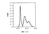
図2は、本発明に係る蛍光体の蛍光スペクトルを示す特性図である。図中の横軸は発光波長を示し、図中の縦軸は各波長の光強度を任意単位で示す。図中の一点鎖線は700℃でのアニールを行う前の焼成物の蛍光スペクトルであり、図中の実線はアニールを行って完成した本発明に係る蛍光体の蛍光スペクトルである。また、本発明の蛍光体はCaS:Eu及びCaGa2 S4 :Euを組成として含んでおり、図中の破線は、本発明の製造方法によらずに個別に製造したCaS:EuとCaGa2S4 :Euとの混合物の蛍光スペクトルである。図2に示した蛍光スペクトルは、波長が470nmの励起光により各試料が発生した蛍光の観測結果である。本発明の蛍光体では、550nmの波長付近にピークを有する緑色蛍光に加えて、650nmの波長付近にピークを有する赤色蛍光が発生しており、アニールを行うことによって赤色蛍光の光強度が増大している。 FIG. 2 is a characteristic diagram showing the fluorescence spectrum of the phosphor according to the present invention. The horizontal axis in the figure indicates the emission wavelength, and the vertical axis in the figure indicates the light intensity of each wavelength in arbitrary units. The one-dot chain line in the figure is the fluorescence spectrum of the fired product before annealing at 700 ° C., and the solid line in the figure is the fluorescence spectrum of the phosphor according to the present invention completed by annealing. The phosphor of the present invention is CaS: Eu and CaGa 2 S 4: Eu and contains a composition, the dashed line in the figure, were prepared individually regardless of the production method of the present invention CaS: Eu and CaGa 2 S 4 : Fluorescence spectrum of a mixture with Eu. The fluorescence spectrum shown in FIG. 2 is an observation result of fluorescence generated by each sample by excitation light having a wavelength of 470 nm. In the phosphor of the present invention, red fluorescence having a peak near the wavelength of 650 nm is generated in addition to the green fluorescence having a peak near the wavelength of 550 nm, and the light intensity of the red fluorescence increases by annealing. ing.
図3は、本発明に係る蛍光体及び従来の蛍光体の蛍光スペクトルを示す特性図である。図中の横軸は発光波長を示し、図中の縦軸は各波長の光強度を任意単位で示す。図中の実線は本発明に係る蛍光体の蛍光スペクトルであり、図中の破線は従来の蛍光体であるYAG:Ceの蛍光スペクトルである。図3に示した蛍光スペクトルは、波長が470nmの励起光により各試料が発生した蛍光の観測結果である。図に示す如く、本発明に係る蛍光体は、従来の蛍光体であるYAG:Ceに比べて、緑色蛍光及び赤色蛍光をより強い光強度で発生することができる。 FIG. 3 is a characteristic diagram showing fluorescence spectra of the phosphor according to the present invention and the conventional phosphor. The horizontal axis in the figure indicates the emission wavelength, and the vertical axis in the figure indicates the light intensity of each wavelength in arbitrary units. The solid line in the figure is the fluorescence spectrum of the phosphor according to the present invention, and the broken line in the figure is the fluorescence spectrum of YAG: Ce, which is a conventional phosphor. The fluorescence spectrum shown in FIG. 3 is an observation result of fluorescence generated by each sample by excitation light having a wavelength of 470 nm. As shown in the figure, the phosphor according to the present invention can generate green fluorescence and red fluorescence with stronger light intensity than YAG: Ce which is a conventional phosphor.
本発明のLEDは、400〜560nmの波長の光を発生するLEDチップ1を用いて構成されている。また被覆部2は、LEDチップ1を凹部3aの底部にダイボンディングした後に、本実施の形態に係る蛍光体を混合したエポキシ樹脂又はシリコーン樹脂等の透光性の樹脂を凹部3a内に充填し、充填した樹脂を加熱して硬化させることにより形成される。LEDチップ1が発生する青色光の一部を被覆部2に含まれる蛍光体が吸収して図3に示す如きスペクトルの光を発生することにより、本発明のLEDは白色光を発生する白色LEDとして機能する。
The LED of the present invention is configured using an
図4は、本発明のLEDの発光スペクトルを示す特性図である。図中に示した発光スペクトルは、479nmの波長に発光のピークを有するLEDチップ1を用いたLEDの発光スペクトルである。図中の実線は本発明の蛍光体を含んだ被覆部2を備える本発明のLEDの発光スペクトルであり、図中の破線は従来の蛍光体であるYAG:Ceを含んだ被覆部2を備える従来のLEDの発光スペクトルである。図中の横軸は発光波長を示し、図中の縦軸は、本発明のLEDと従来のLEDとの波長479nmの光強度が等しいとした場合の各波長の相対的な光強度を示す。本発明のLEDは、緑色領域及び赤色領域で従来のLEDよりも強い発光が得られる。特に、赤色領域の発光が従来に比べて強いので、本発明のLEDは、蛍光体にYAG:Ceを用いた従来のLEDに比べて、光の色度図上で完全な白色を示す色度座標値(x,y)=(0.33,0.33)により近い光を発生することができる。
FIG. 4 is a characteristic diagram showing an emission spectrum of the LED of the present invention. The emission spectrum shown in the figure is an emission spectrum of an LED using the
以上詳述した如く、本発明により、青色光を吸収することにより緑色光及び赤色光を発生する蛍光体を製造することが可能となり、この本発明に係る蛍光体と青色光を発生するLEDチップ1とを組み合わせることにより、白色光を発生するLEDを実現することができる。本発明のLEDが発生する白色光は、赤色成分が多く含まれているので、演色性が向上する。特に人の皮膚の色の再現性が向上するので、本発明のLEDは照明用として好適になる。また本発明のLEDは従来のLEDに比べて相対的に緑色光及び赤色光の光強度が強いので、液晶のバックライトとして利用した場合は、カラーフィルタを用いて効率的に緑色又は赤色の単色光を取り出すことができる。 As described above in detail, according to the present invention, it is possible to manufacture a phosphor that generates green light and red light by absorbing blue light, and the phosphor according to the present invention and an LED chip that generates blue light. In combination with 1, an LED that generates white light can be realized. Since the white light generated by the LED of the present invention contains a lot of red components, the color rendering properties are improved. In particular, since the color reproducibility of human skin is improved, the LED of the present invention is suitable for illumination. In addition, since the LED of the present invention has a relatively strong light intensity of green light and red light compared to conventional LEDs, when used as a liquid crystal backlight, a single color of green or red is efficiently used using a color filter. Light can be extracted.
また本発明に係る蛍光体は、青色光を吸収することにより緑色光を発生し、青色光及び緑色光を吸収して赤色光を発生するので、青色光を直接に吸収して赤色光を発生する赤色蛍光体に比べて非輻射緩和による熱放射量が抑制される。従って、本発明に係る蛍光体を用いた本発明のLEDは、青色光を直接に吸収して赤色光を発生する赤色蛍光体を用いた従来のLEDに比べて、熱によるLEDチップ1及び蛍光体等の劣化が抑制されるので、LEDの寿命をより長くすることができる。
In addition, the phosphor according to the present invention generates green light by absorbing blue light, and generates red light by absorbing blue light and green light. Therefore, red light is generated by directly absorbing blue light. The amount of heat radiation due to non-radiative relaxation is suppressed as compared with the red phosphor. Therefore, the LED of the present invention using the phosphor according to the present invention has the
また本発明に係る蛍光体は、青色光を吸収することにより緑色光及び赤色光を同時に発生する蛍光体であって、緑色光を発生する部分と赤色光を発生する部分とが一体となっているので、被覆部2を形成する樹脂に蛍光体を混合する際に緑色光を発生する部分と赤色光を発生する部分とが樹脂内で互いに不均一になることがない。従って、別個の2種類の蛍光体を用いる従来のLEDに比べて、本実施の形態に係る蛍光体を用いる本発明のLEDは、各色の発光・吸収効率を制御することが容易であるので、発光効率又は色合い等の発光品質を安定させることができる。
The phosphor according to the present invention is a phosphor that simultaneously generates green light and red light by absorbing blue light, and a portion that generates green light and a portion that generates red light are integrated. Therefore, when the phosphor is mixed with the resin forming the covering
なお、本実施の形態では、本発明のLEDとして砲弾型のモールド部6とリードフレーム3及び4とを備えた形態を示したが、本発明のLEDは、これに限るものではなく、その他の形態であってもよい。図5は、本発明のLEDの表面実装型の形態を示す断面図である。図中7は配線基板であり、配線基板7の表面には銅箔による配線パターン71及び72が互いに離隔して形成されている。配線基板7の表面に形成された一方の配線パターン71の表面に、LEDチップ1が実装されている。LEDチップ1の一方の電極は、ワイヤ5により配線パターン71とワイヤボンディングされ、他方の電極はワイヤ5により配線パターン72とワイヤボンディングされている。LEDチップ1の周囲には、本発明に係る蛍光体を含む樹脂にて被覆部2が形成されている。被覆部2は、LEDチップ1の発光面を含む全体を覆っている。更に、被覆部2、ワイヤ5,5、及び配線基板7の表面に形成された配線パターン71,72の一部は、エポキシ樹脂等の樹脂で形成されたモールド部6に覆われている。
In the present embodiment, an embodiment in which the bullet-shaped mold part 6 and the lead frames 3 and 4 are provided as the LED of the present invention is shown, but the LED of the present invention is not limited to this, Form may be sufficient. FIG. 5 is a cross-sectional view showing the surface mount type configuration of the LED of the present invention. In the figure, reference numeral 7 denotes a wiring board. On the surface of the wiring board 7,
この形態においても、400〜560nmの波長の光を発生するLEDチップ1と、本発明に係る蛍光体を含んだ樹脂で形成された被覆部2とを用いることにより、演色性の良い白色光を発生し、寿命が長く、発光品質が安定した表面実装型のLEDを実現することができる。
Also in this embodiment, by using the
(実施の形態2)
本実施の形態においては、実施の形態1に示した蛍光体の製造方法に更に工程を加えた製造方法で蛍光体を製造する。本実施の形態に係る蛍光体を用いることによって白色光を発生する本発明のLEDの構成は、図1又は図5に示した実施の形態1と同様であるので、その説明を省略する。
(Embodiment 2)
In the present embodiment, the phosphor is manufactured by a manufacturing method in which a process is further added to the manufacturing method of the phosphor shown in the first embodiment. The configuration of the LED of the present invention that generates white light by using the phosphor according to the present embodiment is the same as that of the first embodiment shown in FIG. 1 or FIG.
以下に、本実施の形態に係る蛍光体の製造方法を説明する。原料として、CaSとGa2 S3 とのモル比が所定の混合比35:65となるようにCaSとGa2 S3 との粉末を秤量混合し、更に0.01モル比のEuSの粉末を混合した。この原料粉末の混合物1gを、一端を封じた内径7mmのシリカチューブに投入した。このシリカチューブを真空ポンプに接続してシリカチューブ内を10-2torr以下まで減圧した後、150℃で8時間の脱水処理を行った。次に、シリカチューブ内の原料粉末の混合物を真空封入した。 Below, the manufacturing method of the fluorescent substance which concerns on this Embodiment is demonstrated. As a raw material, powders of CaS and Ga 2 S 3 are weighed and mixed so that the molar ratio of CaS and Ga 2 S 3 is a predetermined mixing ratio of 35:65, and EuS powder of 0.01 molar ratio is further mixed. Mixed. 1 g of this raw material powder mixture was put into a silica tube having an inner diameter of 7 mm and sealed at one end. This silica tube was connected to a vacuum pump, and the inside of the silica tube was depressurized to 10 −2 torr or less, followed by dehydration at 150 ° C. for 8 hours. Next, the raw material powder mixture in the silica tube was vacuum sealed.
次に、原料粉末の混合物を真空封入したシリカチューブを電気炉内に置き、10℃/分の昇温スピードで900℃まで昇温した。900℃で30分間温度を保持した後、10℃/分の昇温スピードでシリカチューブを1000〜1100℃まで昇温した。次に、1000〜1100℃でシリカチューブを30分間保持した後、シリカチューブを900℃〜1000℃まで冷却し、900℃〜1000℃でシリカチューブを30分間保持する。次に、電気炉のスイッチをオフにし、電気炉内でシリカチューブを冷却した。シリカチューブを室温まで冷却した後、シリカチューブの温度を再び上昇させ、700℃で60分間温度を保持することによって、シリカチューブ内の生成物のアニールを行った。アニールを行った後の生成物が本実施の形態に係る蛍光体である。 Next, the silica tube in which the mixture of the raw material powders was vacuum-sealed was placed in an electric furnace, and the temperature was raised to 900 ° C. at a temperature raising rate of 10 ° C./min. After maintaining the temperature at 900 ° C. for 30 minutes, the silica tube was heated to 1000 to 1100 ° C. at a heating rate of 10 ° C./min. Next, after holding a silica tube at 1000-1100 degreeC for 30 minutes, a silica tube is cooled to 900 to 1000 degreeC, and a silica tube is hold | maintained at 900 to 1000 degreeC for 30 minutes. Next, the switch of the electric furnace was turned off, and the silica tube was cooled in the electric furnace. After the silica tube was cooled to room temperature, the temperature of the silica tube was increased again, and the product in the silica tube was annealed by maintaining the temperature at 700 ° C. for 60 minutes. The product after annealing is the phosphor according to the present embodiment.
CaS、Ga2 S3 及びEuSの混合物は、1000〜1100℃で焼成することでCaS:Euの結晶とCaGa2 S4 :Euの結晶とが析出する。1000〜1100℃まで昇温した混合物を900℃〜1000℃で保持することにより、焼成による生成物の液相中でCaS:Euの結晶が成長する。CaS:Euの結晶が成長した生成物を室温まで冷却し更に700℃でアニールすることで、CaS:Eu及びCaGa2 S4 :Euの結晶性が整い、900℃〜1000℃で析出したCaS:Euの結晶をコアとしてその周囲にCaGa2 S4:Euの結晶が析出した蛍光体が製造される。CaS:Euは比較的耐水性が悪いので、CaS:Euの周囲を比較的耐水性が良いCaGa2 S4:Euが囲んで保護する蛍光体は、実施の形態1に係る蛍光体に比べて耐水性に優れている。従って、本実施の形態に係る蛍光体は実施の形態1に係る蛍光体に比べて水蒸気に対する耐久性が高いので、本実施の形態に係る蛍光体を用いた本発明のLEDは、実施の形態1に係る蛍光体を用いたLEDに比べて寿命が長くなる。 When a mixture of CaS, Ga 2 S 3 and EuS is baked at 1000 to 1100 ° C., CaS: Eu crystals and CaGa 2 S 4 : Eu crystals are precipitated. By holding the mixture heated to 1000 to 1100 ° C. at 900 to 1000 ° C., crystals of CaS: Eu grow in the liquid phase of the product obtained by firing. The product in which the crystals of CaS: Eu have grown is cooled to room temperature and further annealed at 700 ° C., so that the crystallinity of CaS: Eu and CaGa 2 S 4 : Eu is adjusted, and CaS precipitated at 900 ° C. to 1000 ° C .: A phosphor is produced in which a crystal of CaGa 2 S 4 : Eu is deposited around an Eu crystal as a core. Since CaS: Eu has relatively poor water resistance, the phosphor that protects CaS 2: Eu surrounded by CaGa 2 S 4 : Eu that has relatively good water resistance as compared with the phosphor according to the first embodiment. Excellent water resistance. Therefore, since the phosphor according to the present embodiment has higher durability against water vapor than the phosphor according to the first embodiment, the LED of the present invention using the phosphor according to the present embodiment is The lifetime is longer than that of the LED using the phosphor according to 1.
本実施の形態に係る蛍光体の蛍光スペクトルは、実施の形態1と同様であり、従って、本実施の形態に係る蛍光体を用いたLEDは、実施の形態1と同様に、演色性の良い白色光を発生することができる。また実施の形態1と同様に、本実施の形態に係る蛍光体は、CaSとGa2 S3 とEuSとのモル比をx:y:zとして、x+y+z=100、0.01≦z≦10、33≦x+z≦90、10≦y≦67とした割合の混合物を焼成することで製造することもできる。また同様に、本実施の形態に係る蛍光体は、焼成時の温度は800〜1100℃の範囲の温度であってもよく、アニール時の温度は600〜900℃の範囲の温度であってもよい。 The fluorescence spectrum of the phosphor according to the present embodiment is the same as that of the first embodiment. Therefore, the LED using the phosphor according to the present embodiment has good color rendering properties as in the first embodiment. White light can be generated. Similarly to the first embodiment, the phosphor according to the present embodiment has x: y: z = 100, 0.01 ≦ z ≦ 10, where the molar ratio of CaS, Ga 2 S 3 and EuS is x: y: z. , 33 ≦ x + z ≦ 90, and 10 ≦ y ≦ 67. Similarly, in the phosphor according to the present embodiment, the firing temperature may be in the range of 800 to 1100 ° C., and the annealing temperature may be in the range of 600 to 900 ° C. Good.
1 LEDチップ(発光ダイオード素子)
2 被覆部
1 LED chip (light-emitting diode element)
2 Covering part
Claims (5)
xモル比のCaS、yモル比のGa2 S3 及びzモル比のEuSを混合する過程と、
該過程後の生成物を800〜1100℃の温度で所定時間保持する過程と、
該過程後の生成物を冷却する過程と、
該過程後の生成物の温度を再度上昇させて600〜900℃の温度で所定時間保持する過程と
を含むことを特徴とする蛍光体の製造方法。
但し、x+y+z=100、0.01≦z≦10、33≦x+z≦90、10≦y≦67とする。 In the method for producing a phosphor formed by firing a mixture containing CaS, Ga 2 S 3 and EuS,
mixing x molar ratio CaS, y molar ratio Ga 2 S 3 and z molar ratio EuS;
Holding the product after the process at a temperature of 800 to 1100 ° C. for a predetermined time;
Cooling the product after the process;
And raising the temperature of the product after the process again and holding it at a temperature of 600 to 900 ° C. for a predetermined time.
However, x + y + z = 100, 0.01 ≦ z ≦ 10, 33 ≦ x + z ≦ 90, and 10 ≦ y ≦ 67.
xモル比のCaS、yモル比のGa2 S3 及びzモル比のEuSを混合する過程と、
該過程後の生成物を1000〜1100℃の温度で所定時間保持する過程と、
該過程後の生成物を900〜1000℃の温度で所定時間保持する過程と、
該過程後の生成物を冷却する過程と、
該過程後の生成物の温度を再度上昇させて600〜900℃の温度で所定時間保持する過程と
を含むことを特徴とする蛍光体の製造方法。
但し、x+y+z=100、0.01≦z≦10、33≦x+z≦90、10≦y≦67とする。 In the method for producing a phosphor formed by firing a mixture containing CaS, Ga 2 S 3 and EuS,
mixing x molar ratio CaS, y molar ratio Ga 2 S 3 and z molar ratio EuS;
Holding the product after the process at a temperature of 1000 to 1100 ° C. for a predetermined time;
Holding the product after the process at a temperature of 900 to 1000 ° C. for a predetermined time;
Cooling the product after the process;
And raising the temperature of the product after the process again and holding it at a temperature of 600 to 900 ° C. for a predetermined time.
However, x + y + z = 100, 0.01 ≦ z ≦ 10, 33 ≦ x + z ≦ 90, and 10 ≦ y ≦ 67.
4. A phosphor manufacturing method according to claim 2, comprising: a light emitting diode element that generates light having a wavelength of 400 to 560 nm; and a covering portion that covers a part or all of the light emitting diode element. A light emitting diode comprising a phosphor manufactured in (1).
Priority Applications (1)
| Application Number | Priority Date | Filing Date | Title |
|---|---|---|---|
| JP2004248852A JP3987515B2 (en) | 2004-08-27 | 2004-08-27 | Phosphor, phosphor manufacturing method, and light emitting diode |
Applications Claiming Priority (1)
| Application Number | Priority Date | Filing Date | Title |
|---|---|---|---|
| JP2004248852A JP3987515B2 (en) | 2004-08-27 | 2004-08-27 | Phosphor, phosphor manufacturing method, and light emitting diode |
Publications (2)
| Publication Number | Publication Date |
|---|---|
| JP2006063225A JP2006063225A (en) | 2006-03-09 |
| JP3987515B2 true JP3987515B2 (en) | 2007-10-10 |
Family
ID=36109986
Family Applications (1)
| Application Number | Title | Priority Date | Filing Date |
|---|---|---|---|
| JP2004248852A Expired - Fee Related JP3987515B2 (en) | 2004-08-27 | 2004-08-27 | Phosphor, phosphor manufacturing method, and light emitting diode |
Country Status (1)
| Country | Link |
|---|---|
| JP (1) | JP3987515B2 (en) |
Families Citing this family (7)
| Publication number | Priority date | Publication date | Assignee | Title |
|---|---|---|---|---|
| JP5578597B2 (en) | 2007-09-03 | 2014-08-27 | 独立行政法人物質・材料研究機構 | Phosphor, method for manufacturing the same, and light emitting device using the same |
| JP2009117160A (en) * | 2007-11-06 | 2009-05-28 | Kyoto Institute Of Technology | LED lighting device |
| JP5192854B2 (en) * | 2008-03-06 | 2013-05-08 | 日本放送協会 | Phosphor and display panel using the same |
| JP5171326B2 (en) * | 2008-03-13 | 2013-03-27 | 住友金属鉱山株式会社 | Method for manufacturing phosphor for inorganic EL |
| JP5641384B2 (en) | 2008-11-28 | 2014-12-17 | 独立行政法人物質・材料研究機構 | LIGHTING DEVICE FOR DISPLAY DEVICE AND DISPLAY DEVICE |
| JP6361416B2 (en) * | 2014-09-24 | 2018-07-25 | 堺化学工業株式会社 | Method for producing red phosphor |
| JP6512070B2 (en) * | 2015-11-09 | 2019-05-15 | 堺化学工業株式会社 | Red phosphor |
-
2004
- 2004-08-27 JP JP2004248852A patent/JP3987515B2/en not_active Expired - Fee Related
Also Published As
| Publication number | Publication date |
|---|---|
| JP2006063225A (en) | 2006-03-09 |
Similar Documents
| Publication | Publication Date | Title |
|---|---|---|
| US7651634B2 (en) | Phosphor composition and method for producing the same, and light-emitting device using the same | |
| EP1802728B1 (en) | Phosphor and light emitting device using the same | |
| US7088038B2 (en) | Green phosphor for general illumination applications | |
| KR100841677B1 (en) | Light emitting device and lighting device | |
| JP5216330B2 (en) | Illumination system including radiation source and luminescent material | |
| JP5450625B2 (en) | Light emitting device | |
| KR20100015323A (en) | Red line emitting phosphors for use in led applications | |
| WO2005078811A1 (en) | Light emitting device and lighting fixture | |
| WO2005017066A1 (en) | Deep red phosphor for general illumination applications | |
| CN101138278A (en) | Illumination systems including radiation sources and fluorescent materials | |
| WO2008057225A2 (en) | High cri led lamps utilizing single phosphor | |
| US20120062103A1 (en) | Red light-emitting fluorescent substance and light-emitting device employing the same | |
| JP3987515B2 (en) | Phosphor, phosphor manufacturing method, and light emitting diode | |
| JP2010155891A (en) | Nitride red phosphor and white light emitting diode utilizing the same | |
| KR101176212B1 (en) | Alkali-earth Phosporus Nitride system phosphor, manufacturing method thereof and light emitting devices using the same | |
| JP5125039B2 (en) | Rare earth oxynitride phosphor and light emitting device using the same | |
| JP3987516B2 (en) | Phosphor and light emitting diode | |
| JP5194395B2 (en) | Oxynitride phosphor and light-emitting device using the same | |
| JP4119734B2 (en) | Phosphor, light emitting diode, and method for producing phosphor | |
| KR101014076B1 (en) | Phosphor, Light Emitting Device and Phosphor Manufacturing Method | |
| KR100788041B1 (en) | Ceramic phosphor for manufacturing white light emitting diode and white light emitting diode using same | |
| KR100658458B1 (en) | Yellow red phosphor, white LED element and yellow red LED element using same | |
| KR101227403B1 (en) | Phosphors thin film for white light emitting diode and white light emitting diode fabricated using the same | |
| KR100670478B1 (en) | Light emitting element | |
| JP2022163455A (en) | Phosphor and light-emitting device including the same |
Legal Events
| Date | Code | Title | Description |
|---|---|---|---|
| A977 | Report on retrieval |
Free format text: JAPANESE INTERMEDIATE CODE: A971007 Effective date: 20061130 |
|
| A131 | Notification of reasons for refusal |
Free format text: JAPANESE INTERMEDIATE CODE: A131 Effective date: 20070109 |
|
| A256 | Written notification of co-pending application filed on the same date by different applicants |
Free format text: JAPANESE INTERMEDIATE CODE: A2516 Effective date: 20070109 |
|
| A521 | Request for written amendment filed |
Free format text: JAPANESE INTERMEDIATE CODE: A523 Effective date: 20070307 |
|
| TRDD | Decision of grant or rejection written | ||
| A01 | Written decision to grant a patent or to grant a registration (utility model) |
Free format text: JAPANESE INTERMEDIATE CODE: A01 Effective date: 20070703 |
|
| A61 | First payment of annual fees (during grant procedure) |
Free format text: JAPANESE INTERMEDIATE CODE: A61 Effective date: 20070712 |
|
| R150 | Certificate of patent or registration of utility model |
Ref document number: 3987515 Country of ref document: JP Free format text: JAPANESE INTERMEDIATE CODE: R150 |
|
| FPAY | Renewal fee payment (event date is renewal date of database) |
Free format text: PAYMENT UNTIL: 20100720 Year of fee payment: 3 |
|
| FPAY | Renewal fee payment (event date is renewal date of database) |
Free format text: PAYMENT UNTIL: 20100720 Year of fee payment: 3 |
|
| FPAY | Renewal fee payment (event date is renewal date of database) |
Free format text: PAYMENT UNTIL: 20130720 Year of fee payment: 6 |
|
| R250 | Receipt of annual fees |
Free format text: JAPANESE INTERMEDIATE CODE: R250 |
|
| R250 | Receipt of annual fees |
Free format text: JAPANESE INTERMEDIATE CODE: R250 |
|
| R250 | Receipt of annual fees |
Free format text: JAPANESE INTERMEDIATE CODE: R250 |
|
| R250 | Receipt of annual fees |
Free format text: JAPANESE INTERMEDIATE CODE: R250 |
|
| R250 | Receipt of annual fees |
Free format text: JAPANESE INTERMEDIATE CODE: R250 |
|
| R250 | Receipt of annual fees |
Free format text: JAPANESE INTERMEDIATE CODE: R250 |
|
| R250 | Receipt of annual fees |
Free format text: JAPANESE INTERMEDIATE CODE: R250 |
|
| R250 | Receipt of annual fees |
Free format text: JAPANESE INTERMEDIATE CODE: R250 |
|
| R250 | Receipt of annual fees |
Free format text: JAPANESE INTERMEDIATE CODE: R250 |
|
| R250 | Receipt of annual fees |
Free format text: JAPANESE INTERMEDIATE CODE: R250 |
|
| LAPS | Cancellation because of no payment of annual fees |