JP3982662B2 - Reception method and high-frequency signal receiver - Google Patents
Reception method and high-frequency signal receiver Download PDFInfo
- Publication number
- JP3982662B2 JP3982662B2 JP23803398A JP23803398A JP3982662B2 JP 3982662 B2 JP3982662 B2 JP 3982662B2 JP 23803398 A JP23803398 A JP 23803398A JP 23803398 A JP23803398 A JP 23803398A JP 3982662 B2 JP3982662 B2 JP 3982662B2
- Authority
- JP
- Japan
- Prior art keywords
- signal
- signals
- frequency signal
- amplitude
- analog
- Prior art date
- Legal status (The legal status is an assumption and is not a legal conclusion. Google has not performed a legal analysis and makes no representation as to the accuracy of the status listed.)
- Expired - Fee Related
Links
- 238000000034 method Methods 0.000 title claims description 42
- 238000012545 processing Methods 0.000 claims description 18
- 230000003111 delayed effect Effects 0.000 claims description 16
- 238000004364 calculation method Methods 0.000 claims description 12
- 238000006243 chemical reaction Methods 0.000 claims description 9
- 238000005070 sampling Methods 0.000 claims description 7
- 230000010363 phase shift Effects 0.000 claims description 5
- 230000001934 delay Effects 0.000 claims description 2
- 238000001514 detection method Methods 0.000 description 31
- 238000010586 diagram Methods 0.000 description 15
- 230000001427 coherent effect Effects 0.000 description 6
- 230000001360 synchronised effect Effects 0.000 description 6
- 230000005540 biological transmission Effects 0.000 description 4
- 238000004891 communication Methods 0.000 description 3
- 230000006870 function Effects 0.000 description 3
- 230000007423 decrease Effects 0.000 description 2
- 238000013461 design Methods 0.000 description 2
- 230000000694 effects Effects 0.000 description 2
- 238000005516 engineering process Methods 0.000 description 2
- 238000001914 filtration Methods 0.000 description 2
- JBRZTFJDHDCESZ-UHFFFAOYSA-N AsGa Chemical compound [As]#[Ga] JBRZTFJDHDCESZ-UHFFFAOYSA-N 0.000 description 1
- 229910001218 Gallium arsenide Inorganic materials 0.000 description 1
- 230000002238 attenuated effect Effects 0.000 description 1
- 239000003990 capacitor Substances 0.000 description 1
- 230000008878 coupling Effects 0.000 description 1
- 238000010168 coupling process Methods 0.000 description 1
- 238000005859 coupling reaction Methods 0.000 description 1
- 238000004519 manufacturing process Methods 0.000 description 1
- 238000005259 measurement Methods 0.000 description 1
- 230000010355 oscillation Effects 0.000 description 1
- 230000035945 sensitivity Effects 0.000 description 1
- 229910052710 silicon Inorganic materials 0.000 description 1
- 239000010703 silicon Substances 0.000 description 1
- 239000000758 substrate Substances 0.000 description 1
- 230000002123 temporal effect Effects 0.000 description 1
Images


Classifications
-
- H—ELECTRICITY
- H04—ELECTRIC COMMUNICATION TECHNIQUE
- H04L—TRANSMISSION OF DIGITAL INFORMATION, e.g. TELEGRAPHIC COMMUNICATION
- H04L27/00—Modulated-carrier systems
-
- H—ELECTRICITY
- H04—ELECTRIC COMMUNICATION TECHNIQUE
- H04L—TRANSMISSION OF DIGITAL INFORMATION, e.g. TELEGRAPHIC COMMUNICATION
- H04L27/00—Modulated-carrier systems
- H04L27/18—Phase-modulated carrier systems, i.e. using phase-shift keying
- H04L27/22—Demodulator circuits; Receiver circuits
- H04L27/233—Demodulator circuits; Receiver circuits using non-coherent demodulation
- H04L27/2331—Demodulator circuits; Receiver circuits using non-coherent demodulation wherein the received signal is demodulated using one or more delayed versions of itself
-
- H—ELECTRICITY
- H03—ELECTRONIC CIRCUITRY
- H03D—DEMODULATION OR TRANSFERENCE OF MODULATION FROM ONE CARRIER TO ANOTHER
- H03D1/00—Demodulation of amplitude-modulated oscillations
- H03D1/22—Homodyne or synchrodyne circuits
- H03D1/2245—Homodyne or synchrodyne circuits using two quadrature channels
-
- H—ELECTRICITY
- H04—ELECTRIC COMMUNICATION TECHNIQUE
- H04B—TRANSMISSION
- H04B1/00—Details of transmission systems, not covered by a single one of groups H04B3/00 - H04B13/00; Details of transmission systems not characterised by the medium used for transmission
- H04B1/06—Receivers
- H04B1/16—Circuits
- H04B1/30—Circuits for homodyne or synchrodyne receivers
Landscapes
- Engineering & Computer Science (AREA)
- Computer Networks & Wireless Communication (AREA)
- Signal Processing (AREA)
- Power Engineering (AREA)
- Digital Transmission Methods That Use Modulated Carrier Waves (AREA)
- Superheterodyne Receivers (AREA)
- Mobile Radio Communication Systems (AREA)
Description
【0001】
【発明の属する技術分野】
本発明は、高周波数信号を受信し、直接変換することによって復調する受信方法及び受信機に関する。
【0002】
【従来の技術】
いわゆるデジタルシグナルプロセッサ(以下、DSP:digital signal processorという。)に接続された6ポート受信回路が知られており、この6ポート受信回路は、マイクロ波帯からミリ波帯におよぶ周波数帯域の信号を、直接、デジタル的に復調することができるようになっている。この新たなダイレクトデジタル受信機は、従来のヘテロダイン受信機に比して、受信機の構成を簡単なものとすることができるとともに、製造における仕様が緩く、高性能で、コスト効率がよく、様々なデジタル端末において使用されている。
【0003】
衛星通信や個人通信装置のようなデジタル通信装置において最も広く使用されている変調方式は、位相偏移変調(以下、PSK:phase shift keyingという。)である。復調技術としては、同期(コヒーレント:coherent)技術と非同期(非コヒーレント:non-coherentmat又は差動:differential)技術の2つがある。一般的に、同期検波がエラー特性において優れているという特徴があるのに対して、非同期(差動)検波は、受信機の構成が簡単であるという特徴がある。すなわち、同期受信機は、搬送波を再生するための回路が必要であり、その構成がかなり複雑である。マイクロ波帯及びミリ波帯においては、搬送波を直接再生することは、特に難しい。
【0004】
従来のヘテロダイン方式の受信機は、図8に示すように、RF信号の増幅等を行うRF回路31と、受信周波数よりも十分に高い周波数に変換して増幅する第1及び第2の中間周波数回路32,33と、検波や復調等を行うベースバンド回路34とを備える。この受信機の一部、例えばRF回路31〜第2の中間周波数回路33、第1の中間周波数回路32と第2の中間周波数回路33、又は第2の中間周波数回路33は、図9に示すように、1つのDSP35に置き換えることができ、上述した6ポート受信回路は、このDSP35に接続される。
【0005】
図10は、1994年5月にサンディエゴで開催された1994年度IEEEMTTシンポジウムのダイジェスト、第3巻、1659〜1662頁に記載されているウー・ボシッショ(Bossio Wu)の「6ポートダイレクトデジタルミリ波受信機(A six-pole direct digital millimeter wave reciver)」の構成を示すブロック図である。この6ポート受信機は、図10に示すように、6ポート受信回路41と、6ポート受信回路41の各出力をデジタル信号に変換するアナログ/デジタル変換器42と、DSP43と、局部発振器44とを備える。
【0006】
6ポート技術は、振幅と位相の両方の散乱パラメータを正確に測定できる技術として知られている。ヘテロダイン回路の代わりに6ポート受信回路を用いると、6ポートのうちの4ポートにおいて、マイクロ波帯とミリ波帯の電力レベルを直接測定することができる。6ポート受信回路を適切に較正(キャリブレーション)することによって、完全なものとすることができ、広いダイナミックレンジ及び広い周波数範囲において、極めて正確な測定値を得ることができる。6ポート受信回路41は、方向性結合器、電力分配器、ダイオード検出器等のマイクロ波受動回路素子から構成される。6ポート受信回路41は、容易にモノリシックマイクロ波集積回路(MMIC)又はモノリシックハイブリッドマイクロ波集積回路(MMIC)に集積化することができる。知られている6ポート受信機は、マイクロ波帯及びミリ波帯において、直接位相/振幅復調を行う。従来の受信機におけるI−Q回路は、6ポート受信機とDSPを備える6ポート位相/周波数弁別器で置き換えることができる。デジタル的に復調される入力RF信号は、デジタル的に制御された局部発振器44の出力である搬送波と比較される。具体的には、DSP43は、入力RF信号と局部発振器44からの搬送波の周波数の違いを検出し、搬送波が入力RF信号に追従するように局部発振器44を制御する。一旦搬送波が正しく再生されると、受信RF信号の瞬時の位相が検出されて、復調され、元の変調されたデータが再生される。最大データ伝送レートは、主に、A/D変換器42のサンプリングレート及びDSP43の処理速度によって決定される。
【0007】
ハードウェア回路のブリッジの位相誤差、電力検出器のばらつき等は、キャリブレーションによって、予め修正することができる。すなわち、ハードウェアの設計仕様は、かなり緩いものとすることができ、また、6ポート受信機を、ミリ波帯までの広い周波数帯域において、動作させることができる。6ポート受信機では、各位相における振幅は、独立して検出されるので、入力RF信号の振幅が広いダイナミックレンジにおいて変化するときでも、入力RF信号の位相偏移変調を正確に検出することができる。また、DSP43のアルゴリズムを予め少し変えるだけで、異なる変調方式にも対応することができる。
【0008】
【発明が解決しようとする課題】
図10に示す6ポート受信機は、同期(コヒーレント)受信機であるので、局部発振器44を必要とし、その構成は非常に複雑であり、1つのチップに集積化できないという問題がある。
【0009】
本発明は、上述のような実情に鑑みてなされたものであり、本発明の目的は、コストが安く、また構造が簡単であって、高周波信号を受信し、直接変換することによって復調する受信方法及び高周波信号受信機を提供することである。また、本発明の目的は、同期(コヒーレント)検波方式に替えて、非同期(非コヒーレント)検波方式を用いた受信方法及び高周波信号受信機を提供することである。
【0010】
【課題を解決するための手段】
本発明に係る受信方法は、入力高周波信号を、2つの信号(S1,S2)に分割するステップと、分割された2つの信号(S1,S2)をそれぞれの所定の遅延時間遅延するステップと、それぞれ遅延された2つの信号(S1,S2)を異なる比率で線形結合して、4つの結合信号を生成するとともに、4つの結合信号の振幅に対応した4つの電力レベル(P1,P2,P3,P4)を計算するステップと、4つの電力レベル(P1,P2,P3,P4)に基づいて、それぞれ遅延された信号(S1)と信号(S2)との関係を示す複素信号の位相及び振幅を計算するステップとを有する。
【0011】
また、本発明に係る変調高周波信号を受信する受信方法は、入力変調高周波信号を、2つの信号(S1,S2)に分割するステップと、分割された2つの信号(S1,S2)をそれぞれの所定の遅延時間遅延するステップと、それぞれ遅延された2つの信号(S1,S2)を異なる比率で線形結合して、4つの結合信号を生成するとともに、4つの結合信号の振幅に対応した4つの電力レベル(P1,P2,P3,P4)を計算するステップと、4つの電力レベルをアナログ的に比較判定することによって、入力変調高周波信号を復調するステップとを有する。
【0012】
また、本発明に係る高周波信号受信機は、入力高周波信号を、2つの信号(S1,S2)に分割する電力分配手段と、信号(S1)と信号(S2)との相対遅延時間が所定の遅延時間となるように、信号(S1,S2)を遅延する少なくとも1つの遅延手段と、それぞれ遅延された信号(S1)と信号(S2)を異なる比率で線形結合して、4つの結合信号を生成するとともに、4つの結合信号の振幅に対応した4つの電力レベル(P1,P2,P3,P4)を計算する計算手段と、4つの電力レベルに基づいて、それぞれ遅延された信号(S1)と信号(S2)との関係を示す複素信号の位相及び振幅を計算する処理手段とを備える。
【0013】
【発明の実施の形態】
以下、本発明に係る受信方法及び高周波信号受信機について、図面を参照しながら説明する。図1は、本発明を適用し、非同期(非コヒーレント)検波方式を採用したダイレクト6ポート受信機の具体的な構成を示すブロック図である。
【0014】
このダイレクト6ポート受信機は、図1に示すように、目的の帯域のRF信号を通過させるバンドパスフィルタ(以下、BPFという。)11と、受信RF信号を増幅する低雑音増幅器(以下、LNAという。)12と、希望波のみを通過させるBPF13と、RF信号を2つ信号S1,S2に分岐する電力分配器14と、信号S1を遅延する遅延線15と、信号S2を遅延する遅延線16と、信号S1と信号S2を線形結合する受動回路17と、4つの電力検出回路18と、4つのアナログ/デジタル変換器(以下、A/D変換器という。)19と、デジタルシグナルプロセッサ(以下、DSP:digital signal processorという。)20とを備える。
【0015】
例えばアンテナで受信されたRF信号は、BPF11に供給され、BPF11は、目的の帯域のRF信号のみを通過させて、LNA12に供給する。LNA12は、受信RF信号を増幅して、BPF13に供給する。BPF13は、例えばBPF11よりも狭い通過帯域を有し、希望波のRF信号のみを通過させて、電力分配器14に供給する。
【0016】
電力分配器14は、BPF13からのRF信号を2つの信号S1と信号S2に分岐し、信号S1を遅延線15に、信号S2を遅延線16に分配する。遅延線15は、遅延係数又は遅延時間τ1を有しており、信号S1を遅延して受動回路17に供給する。遅延線16は、遅延時間τ1とは異なる遅延時間τ2を有しており、信号S2を遅延して受動回路17に供給する。
【0017】
受動回路17は、例えば検出用のダイオード等の線形受動素子のみからなり、信号S1と信号S2を異なる比率で線形結合した4つの結合信号を生成して出力する。
【0018】
4つの電力検出回路18は、例えば検出用のダイオードのみからなり、受動回路17から出力される4つの結合信号の振幅、すなわち電力をそれぞれ検出し、得られる各電力レベルを4つのA/D変換器19にそれぞれ供給する。なお、結合信号の数を、最小の3つとしたときは、電力検出回路18及びA/D変換器19も3個となる。
【0019】
各A/D変換器19は、例えばその内部にLPFや直流(DC)増幅器を備え、各電力検出回路18で検出された電力レベルを増幅するとともに、デジタル信号に変換してDSP20に供給する。DSP20は、デジタル信号に変換された各電力レベルをデジタルフィルタリングするとともに、後述するように、ダイレクト6ポート受信機のキャリブレーションを行い、また、いわゆるIデータ、Qデータを求める演算を行って、入力されたRF信号を復調する。
【0020】
図1に示すように、本発明を適用したダイレクト6ポート受信機は、受動素子から構成され、RF帯域の2つの信号が入力される受動回路17を備える。この受動回路17は、目的とする周波数帯域に依存して、例えば数百kHzから数百MHzの周波数帯域において機能するように設計されている。受動回路17には、4つの電力検出回路18が接続されており、電力検出回路18の出力は、DC電圧であり、A/D変換器19によって適切に増幅され、フィルタリングされた後、サンプリングされてデジタル信号に変換される。
【0021】
本発明の重要な特徴は、2つの遅延線15,16を備え、従来の局部発振器を不要とすることである。2つの遅延線15,16によって、電力分配器14で分岐されたRF信号の2つの信号S1と信号S2の相対遅延時間は、Δτ=τ1−τ2である。この相対遅延時間Δτは、A/D変換器19のサンプリングレートの逆数以上とされる。なお、遅延線16の遅延時間を0としてもよく、この場合、遅延線16は不要である。
【0022】
以上の説明でも明らかなように、本発明では、図1に示すように、ベクトル情報、すなわちRF信号のある振幅における位相を、電力検出回路18によって検出された電力レベルであるスカラー情報のみに基づいて検出することができる。したがって、本発明では、非コヒーレントに位相情報を検出することができる。遅延線15,16によってそれぞれ遅延された2つの信号S1,S2の比率については、後述する。
【0023】
従来の装置にない本発明の特徴は、例えば位相及び振幅がアンバランスである等の不完全なハードウェアを、物理的接続を変更することなく、キャリブレーションによって調整できることであり、RF素子の公差を大きくして設計仕様を緩くすることができる。また、非同期復調を行うので、局部発振器は不必要である。一方、従来の装置は、RFレベルと同じくらいの低電力の局部発振器を必要とし、また、自動周波数(位相)制御をデジタル的に処理する回路が必要であった。
【0024】
また、本発明の特徴は、局部発振器を必要としないので、全てのRFフロントエンドを簡単にICチップで実現することができる。従来、低周波帯域では、GAAS(ガリューム砒素)又はSI(シリコン)のモノリシックマイクロ波集積回路(MMIC)技術を用いる必要がなかったが、本発明を適用したダイレクト6ポート受信機でも、より周波数が高い帯域で用いられるにもかかわらず、能動素子がなく、また電波を検出するの検出ダイオードのみを用いているので、このことを適用することができる。すなわち、本発明では、中間周波数回路、局部発振器、AGC、PLL等を必要とせず、簡単な構成でRFフロントエンドを実現でき、コストの削減を図ることができる。
【0025】
なお、図1に示す具体例では、検出された電力レベルをA/D変換器19によってデジタル信号に変換した後、処理を行うようにしているが、例えば入力RF信号を簡単な復調方法で復調することができるときは、検出された電力レベルをデジタル信号に変換する必要はなく、そのまま処理するようにしてもよい。
【0026】
いずれにせよ、DSP20において、電力分配器14によって分岐された2つの入力RF信号の比率を示す複素信号には、キャリブレーションによって得られたキャリブレーション係数を用いて、演算処理が施される。そして、複素信号は、さらにI/Qデータに分解され、従来の復調処理によって、ベースバンドのデータに変換される。
【0027】
また、LNA12及びBPF13,14を、遅延線15,16の後段に配置したり、又は遅延線15,16と伴に集積化して、受動回路17の入力に設けるようにしてもよい。
【0028】
ここで、本発明を適用したダイレクト6ポート受信機を構成する電気素子について、詳細に説明する。
【0029】
受動回路17は、線形の受動素子のみを有する回路からなり、様々な素子及び組立技術を用いることにより、その中に、電力分配器、ハイブリッド回路、結合器、伝送線路、結合素子、抵抗器、コンデンサを組み込むことができる。全ての受動回路は、個々の素子又は集中常数(lump)素子から構成することができる。伝送線路、基板、集中常数素子をどの様に設計するかは、目的とする周波数帯域、例えば以下に説明するRF周波数帯域に対応するようにされるが、通常最適化が図られる。
【0030】
RF周波数帯域が、目的とする帯域である。このRF周波数帯域において、本発明に適用したダイレクト6ポート受信機が動作する。RF周波数帯域は、中間周波数帯域であり、受信機の回路は、他の帯域よりもより複雑になることが知られている。この中間周波数においては、本発明を適用したダイレクト6ポート受信機は、受信信号を中間周波数帯域から直接ベースバンドに変換する回路として動作する。図3及び図4に示すように、本発明を適用したダイレクト6ポート受信機は、他の中間周波数又はより高いRF周波数の信号から従来のダウンコンバート技術の1つによって得られる中間周波数信号を処理することができる。RF周波数信号は、50MHz〜100GHzの範囲の信号である。RF周波数信号は、受動回路17に入力される前にフィルタリング及び増幅される。なお、BPF11の前段に、必要に応じて、周波数チャンネルを選択するためのBPFを設けるようにしてもよい。
【0031】
上述したように、受動回路17は、遅延線15,16でそれぞれ遅延された2つの信号S1,S2 を異なる比率で線形結合する。これによって得られる4つの信号の各電力レベルをP1,P2,P3,P4とすると、電力レベルP1,P2,P3,P4は、下記式1に示すように、2つの信号S1,S2に基づいて計算される。
【0032】
P1=a×S1+b×S2
P2=c×S1+d×S2
P 3 =e×S1+f×S2
P 4 =g×S1+h×S2 ・・・式1
【0033】
これらの電力レベルP1,P2,P3,P4は、電力検出回路18によって検出される。電力検出回路18は、RF周波数帯域の周波数範囲で入力される信号の電力を、直流(DC)電圧の情報に変換する。ダイレクト6ポート受信機は、様々な技術によって実現することができる。ダイレクト6ポート受信機を実施又は実現する最も一般的な技術は、通常の検出ダイオードによって実現されることである。検出ダイオードは、受動回路17と伴に1つのチップに集積化することができる。なお、検出ダイオードの温度変化を補償する回路を設けるようにしてもよい。
【0034】
DSP20は、A/D変換器19によって増幅され、フィルタリングされた後、デジタル信号に変換された電力レベルP1,P2,P3,P4からなる複素信号の演算を行う。この複素信号は、2つの信号S1,S2の比率を示している。DSP20は、A/D変換器19から供給されるデータをデジタル的に信号処理する。DSP20の基本的な機能は、以下の通りである。
・デジタル的にローパスフィルタリングする。
・上述の複素信号の演算を行う。
・キャリブレーションによって得られるキャリブレーション係数の演算を行う。
・必要に応じて、複素信号を実数部及び虚数部(I/Qデータ)に変換する。
【0035】
なお、複素信号の演算とキャリブレーション係数の演算を、DSP20のソフトウェアで行うようにしているが、特定用途向けLSI(ASIC)等のハードウェアで行うようにしてもよい。どちらを用いるかは、処理するデータレートに依存するものである。また、DSP20又はASICにおいて、復調処理も行うようにしてもよい。
【0036】
ここで、DSP20における2つの信号S1,S2の比率を示す複素信号の演算について説明する。複素信号は、DSP20において、キャリブレーション係数と、電力検出回路18によって検出され、電圧の比率として示される電力レベルの組合せとを用いて、計算される。4つの電力検出回路18を用いた場合の複素信号δは、下記式2で表される。
【0037】
【数1】
【0038】
ここで、piは、電力検出回路18で検出された電力レベルの1つを基準として、他の電力レベルをこの基準電力レベルで割った相対値、例えば電力レベルP4を基準とした電力レベルP1の相対値(p1=P1/P4)であり、x(i),x1(i),y(i),y1(i)(i=1,2,3)は、キャリブレーション処理によって得られるキャリブレーション係数である。
【0039】
ξ(τ1)は、遅延時間τ1遅延された信号S1であり、実際には、搬送波の周波数f0でアップコンバートされたベースバンド信号からなる。
【0040】
ξ(τ2)は、遅延時間τ2遅延された信号S2であり、実際には、搬送波の周波数f0でアップコンバートされたベースバンド信号からなる。
【0041】
Δτ=τ1−τ2において、相対遅延時間Δτは、A/D変換器19のサンプリング周期以上であり、また、遅延時間τ1,τ2のいずれか1つは、0としてもよい。
【0042】
遅延時間の差分が乗算された信号の2つのサンプルにおける全体の周波数成分の変化が一定であるとき、又は無視できるとき、1つのサンプルに対する他のサンプルの振幅及び位相の相対的変化に関する情報、又はI/Q信号の相対的な増減が得られる。
【0043】
受動回路17において準定常状態が実質的に得られるように、サンプリング周期を主搬送波の発振周期をよりも十分に長くすると、電力検出回路18において正確な電力レベルの検出を行うことができる。
【0044】
キャリブレーション処理は、キャリブレーション係数x(i),x 1 (i),y(i),y 1 (i)を得るために必要な処理である。キャリブレーション処理は、装置の物理的接続を外すことなく行うことができる。また、キャリブレーション処理は、ダイレクト6ポート受信機をオフラインとした状態で行うことができる。すなわち、システムパラメータは、余り速く変化しないので、オフラインでの演算は、信号シンボルの継続時間よりも長い時間Tにおいて行うことができる。
【0045】
キャリブレーション係数は、キャリブレーション処理によって得られ、これらのキャリブレーション係数は、複素数とされ、相対電力に乗算される。初期のキャリブレーション係数をメモリに予め記憶しておき、キャリブレーション処理を行う前は、このキャリブレーション係数を用いて相対電力の計算を行い、キャリブレーション処理を行った後には、メモリを更新して、新たなキャリブレーション係数を用いて相対電力の計算を行うようにする。
【0046】
DSP20においてI/Qデータの数学的演算による非同期(非コヒーレント)検波を行った後、復調処理が実行される。なお、復調処理は、例えばI/Q復調チップ(IC)等のハードウェア又は、例えばキャリブレーション係数の演算及び複素信号の演算を行うDSPにおいてソフトウェアを用いて行うようにしてもよい。ここで、幾つかのアプリケーションにおいては、複素信号は、I情報(データ)とQ情報(データ)に分解されることなく、直接復調するために用いられる。本発明で提案している非同期検波では、本質的に、D/A変換する前に、さらには送信機側の変調器においてI/Qデータで搬送波を変調するには、差動処理が必要とされる。
【0047】
つぎに、本発明を適用したダイレクト6ポート受信機の受動回路17の具体的な構成について、図2〜図7を参照しながら説明する。なお、以下の具体例では、説明を明確にするために、いわゆるQPSK変調された信号を復調する場合について説明するが、様々な変調を用いても、本発明を適用したダイレクト6ポート受信機の本質的な機能は変わらないことはいうまでもなく、様々な変調方式を組み合わせた場合には、必要に応じてD/A変換器及び送信機の変調器の前段において、差動処理が行われる。また、受動回路17の構成は、変わらないことはいうまでもない。
【0048】
また、以下の具体例では、遅延時間の差分は、サンプリング周期と等しいものとしている。さらに、RF信号は、受動回路17に供給される信号の電力レベルと同じレベルを有するものとしている。また、入力されるRF信号は、送信機で差動変調されており、受動回路17は、キャリブレーション処理が不要な理想的な回路からなるものとする。さらに、電力検出回路18が理想的な線形特性を有するものとすると、受動回路17は、図2に示すように、電力分配器21と、90度ハイブリッド回路22,23,24とを備える。
【0049】
ここで、一定の信号振幅において、4つの電力検出回路18で検出された電力レベルP1,P2,P3,P4に基づき、電力レベルP1で正規化した相対電力と位相差を示す。
【0050】
【表1】
図3は、相対位相差に対する様々な相対電力レベル(電力検出回路18で検出された電圧)を示す図である。この図3において、2つの信号S1,S2は、同じ電力レベルを有し、またサンプル時間においてそれらの振幅は変動しないものとしている。
【0052】
図4は、図3と同様に、相対位相差に対する様々な相対電力レベル(電力検出回路18で検出された電圧)を示す図であるが、信号S1,S2の相対電力レベルを20dBとしたものである。
【0053】
図3及び図4に示すように、入力信号S1,S2の電力レベル差が増加すると、ダイレクト6ポート受信機の感度は低下する。このような状態になるのは、遅延線15,16の一方のみを用い、入力信号S1,S2のうちの遅延された信号が減衰した場合である。
【0054】
なお、相対電力レベルは、RF信号レベルに依存しない。また、位相又は振幅の状態の数が少ないときは、簡単な判定論理回路は、復調を行うアナログ素子を用いて、アナログ電圧(電力レベル)を比較する回路で実現されるので、信号の相対振幅及び位相の演算は不要となる。この例は、DPSK復調において適用される。
【0055】
図5は、ダイレクト6ポート受信機のDSP20において必要とされる本質的な演算結果を示す図である。図5は、2つの信号S1,S2が2つの異なる時点(QPSK変調)において同一の大きさであり、位相差が、測定された電力レベル及び3つの円で示されるキャリブレーション係数を演算することによって得られる7π/8であるときの状態を例として示している。理想的には、3つの円は、1点で交差するのが望ましい。交点がグリッドの中央に接するとき、このようにして生成されるベクトルは、2つの遅延線15,16によって生じた相対遅延で定義される2つの異なる時間増分における信号S1,S2の複素比率を示している。複素値を得るためには、キャリブレーション係数によって定義される円の交点を演算する数学的処理が必要である。
【0056】
図5に示すように、グリッドの基点から3つの円の交点に向かうベクトルは、1単位に対応する長さ(振幅)と、157.5゜(7π/8)の角度を有する。ベクトルが、1単位に対応する長さを有することは、QPSK変調において2つの信号S1,S2が同一の大きさを有する場合である。
【0057】
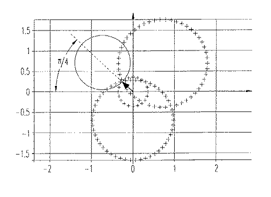
図6は、2つの信号S1,S2の位相及び振幅が異なる例を示す図である。図6は、信号の相対変化が、ある振幅及び45.5°(π/4)の位相において3回あるときの状態を示している。図6に示すように、グリッドの基点から3つの円の交点に向かうベクトルは、1/3単位に相当する長さと、45.5°(π/4)の角度を有する。
【0058】
ここで、演算の結果は、この信号の最終的な複素値ではない。ダイレクト6ポート受信機は、2つの信号S1,S2の差分を検出するので、信号の時間的な相対変化を検出することができる。これは、デジタルデータを、送信機のD/A変換器を介してI/Q変調器に供給し、アップコンバートして伝送の前に、デジタルデータに差動処理を施す必要があることを意味し、DPSK変調方式に本質的に当てはまるものである。伝送されるデジタルデータを差動変調しないときには、変調されたデジタルデータの絶対値を検出するための基準振幅及び基準位相を受信機に通知するために、基準サンプルを伝送する必要がある。
【0059】
実際には、理想的ではなく、3つの円が正確に同一点で交差しない。すなわち、円の交点において、数学的に求めなければならないオフセットが存在する。このオフセットは、キャリブレーション係数が最適化されて得られないという事実に起因している。オフセットの他の原因は、いろんな雑音の影響によるものでる。この場合、DSP20において、例えば図7に示すように、交点をどこにするかを決定するための信号処理を行うようにしてもよい。例えば、湾曲した三角形の中央を、交点としてもよい。なお、オフセットは、QPSK変調方式のように変調状態の数が比較的少ない場合には、無視することができる。
【0060】
【発明の効果】
本発明によれば、コストが安く、また構造が簡単であって、高周波信号を受信し、直接変換することによって復調する受信方法及び高周波信号受信機を提供することができる。
【図面の簡単な説明】
【0061】
【図1】 本発明を適用したダイレクト6ポート受信機の具体的な構成を示すブロック図である。
【図2】 図1に示すダイレクト6ポート受信機の受動回路の具体的な構成を示すブロック図である。
【図3】 分岐された2つのデジタル変調信号の相対位相差に対する、本発明を適用したダイレクト6ポート受信機によって検出された相対電力比を示す図である。
【図4】 分岐された2つのデジタル変調信号の相対電力レベル差が20dBであるときの、相対位相差に対する、本発明を適用したダイレクト6ポート受信機によって検出された相対電力比を示す図である。
【図5】 信号の位相変化及び振幅変化を得るために必要な演算処理の1例を示す図であり、位相変化は、157.5゜(7π/8)の角度であり、振幅は同じである。
【図6】 入力信号の相対変化が、ある振幅及び45.5゜(π/4)の位相において3回あるときの状態を示す図である。
【図7】 図5及び図6に示す円の交点におけるオフセットを整合するための数学的演算を説明するための図である。
【図8】 従来のヘテロダイン型受信機の構成を示すブロック図である。
【図9】 図8に示す各回路をDSPで構成した場合の図である。
【図10】 従来の同期6ポート受信機の構成を示すブロック図である。
【符号の説明】
14 電力分配器、15,16 遅延線、17 受動回路、18 電力検出回路、19 A/D変換器、20 DSP[0001]
BACKGROUND OF THE INVENTION
The present invention relates to a reception method and a receiver that receive and demodulate a high-frequency signal by direct conversion.
[0002]
[Prior art]
A 6-port receiving circuit connected to a so-called digital signal processor (hereinafter referred to as a DSP: digital signal processor) is known, and this 6-port receiving circuit receives a signal in a frequency band from a microwave band to a millimeter wave band. It can be directly demodulated digitally. This new direct digital receiver has a simpler receiver configuration than conventional heterodyne receivers, and has a loose manufacturing specification, high performance, cost efficiency, and variety. Used in various digital terminals.
[0003]
The most widely used modulation method in digital communication devices such as satellite communication and personal communication device is phase shift keying (hereinafter referred to as PSK: phase shift keying). There are two demodulation techniques, a synchronous (coherent) technique and an asynchronous (non-coherentmat or differential) technique. In general, synchronous detection is excellent in error characteristics, whereas asynchronous (differential) detection is characterized in that the configuration of the receiver is simple. That is, the synchronous receiver requires a circuit for reproducing a carrier wave, and its configuration is quite complicated. In the microwave band and the millimeter wave band, it is particularly difficult to directly reproduce the carrier wave.
[0004]
As shown in FIG. 8, a conventional heterodyne receiver includes an
[0005]
Figure 10 is a digest of the 1994 IEEMTT symposium held in San Diego in May 1994, Vol. 3, pages 1659-1662, “6 port direct digital millimeter wave reception” by Bossio Wu It is a block diagram which shows the structure of a machine (A six-pole direct digital millimeter wave reciver). As shown in FIG. 10, the 6-port receiver includes a 6-
[0006]
The 6-port technique is known as a technique that can accurately measure both amplitude and phase scattering parameters. When a 6-port receiving circuit is used instead of the heterodyne circuit,4 of 6 portsIn, it is possible to directly measure the power level of the microwave band and the millimeter wave band. By properly calibrating the 6-port receiver circuit, it can be perfected and very accurate measurements can be obtained in a wide dynamic range and a wide frequency range. The 6-
[0007]
The phase error of the bridge of the hardware circuit, the variation of the power detector, etc. can be corrected in advance by calibration. That is, the hardware design specifications can be quite loose, and the 6-port receiver can be operated in a wide frequency band up to the millimeter wave band. In the 6-port receiver, the amplitude in each phase is detected independently, so that even when the amplitude of the input RF signal changes in a wide dynamic range, the phase shift modulation of the input RF signal can be accurately detected. it can. Also, different modulation schemes can be accommodated by slightly changing the algorithm of the
[0008]
[Problems to be solved by the invention]
Since the 6-port receiver shown in FIG. 10 is a synchronous (coherent) receiver, the
[0009]
The present invention has been made in view of the above-described circumstances, and an object of the present invention is to receive signals that are low in cost and simple in structure, receive high frequency signals, and perform demodulation by direct conversion. It is to provide a method and a high frequency signal receiver. Another object of the present invention is to provide a reception method and a high-frequency signal receiver using an asynchronous (non-coherent) detection method instead of a synchronous (coherent) detection method.
[0010]
[Means for Solving the Problems]
The receiving method according to the present invention converts an input high-frequency signal into two signals (S1, S2) And two divided signals (S1, S2) For each predetermined delay time and two delayed signals (S1, S2) At different ratios,FourGenerate a combined signal,FourCorresponding to the amplitude of the combined signalFourPower level (P1, P2, P3, P4)FourPower level (P1, P2, P3, P4) To each delayed signal (S1) And signal (S2And calculating the phase and amplitude of the complex signal indicating the relationship to
[0011]
The receiving method for receiving a modulated high-frequency signal according to the present invention also converts an input modulated high-frequency signal into two signals (S1, S2) And two divided signals (S1, S2) For each predetermined delay time and two delayed signals (S1, S2) At different ratios,FourGenerate a combined signal,FourCorresponding to the amplitude of the combined signalFourPower level (P1, P2, P3, P4)FourDemodulating the input modulated high frequency signal by comparing and determining the power level in an analog manner.
[0012]
In addition, the high frequency signal receiver according to the present invention converts an input high frequency signal into two signals (S1, S2) And the signal (S1) And signal (S2) With a predetermined delay time so that the signal (S1, S2) And at least one delay means for delaying each of the delayed signals (S1) And signal (S2) At different ratios,FourGenerate a combined signal,FourCorresponding to the amplitude of the combined signalFourPower level (P1, P2, P3, P4)FourBased on the power level, each delayed signal (S1) And signal (S2And processing means for calculating the phase and amplitude of the complex signal indicating the relationship with
[0013]
DETAILED DESCRIPTION OF THE INVENTION
Hereinafter, a receiving method and a high-frequency signal receiver according to the present invention will be described with reference to the drawings. FIG. 1 is a block diagram showing a specific configuration of a direct 6-port receiver to which the present invention is applied and an asynchronous (non-coherent) detection method is adopted.
[0014]
As shown in FIG. 1, the direct 6-port receiver includes a band-pass filter (hereinafter referred to as BPF) 11 that passes an RF signal in a target band, and a low noise amplifier (hereinafter referred to as LNA) that amplifies the received RF signal. 12), BPF 13 that passes only the desired wave, and two RF signals S1, S2A power divider 14 branching into1
[0015]
For example, the RF signal received by the antenna is supplied to the
[0016]
The
[0017]
The
[0018]
The four
[0019]
Each A /
[0020]
As shown in FIG. 1, the direct 6-port receiver to which the present invention is applied includes a
[0021]
An important feature of the present invention is that it includes two
[0022]
As is clear from the above description, in the present invention, as shown in FIG. 1, the vector information, that is, the phase at a certain amplitude of the RF signal is based on only the scalar information that is the power level detected by the
[0023]
A feature of the present invention not found in conventional devices is that incomplete hardware such as, for example, phase and amplitude are unbalanced, can be adjusted by calibration without changing the physical connections, and the tolerance of the RF element The design specification can be relaxed by increasing. Further, since asynchronous demodulation is performed, a local oscillator is unnecessary. On the other hand, the conventional device requires a local oscillator having a power as low as the RF level, and a circuit for digitally processing automatic frequency (phase) control.
[0024]
Further, since the feature of the present invention does not require a local oscillator, all the RF front ends can be easily realized with an IC chip. Conventionally, in the low frequency band, it was not necessary to use GAAS (gallium arsenide) or SI (silicon) monolithic microwave integrated circuit (MMIC) technology. This is applicable because there are no active elements and only detection diodes are used to detect radio waves, even though they are used in a high band. That is, the present invention does not require an intermediate frequency circuit, a local oscillator, an AGC, a PLL, and the like, can realize an RF front end with a simple configuration, and can reduce costs.
[0025]
In the specific example shown in FIG. 1, the detected power level is converted into a digital signal by the A /
[0026]
In any case, in the
[0027]
Further, the LNA 12 and the BPFs 13 and 14 may be arranged at the subsequent stage of the
[0028]
Here, electrical elements constituting the direct 6-port receiver to which the present invention is applied will be described in detail.
[0029]
The
[0030]
The RF frequency band is the target band. In this RF frequency band, the direct 6-port receiver applied to the present invention operates. It is known that the RF frequency band is an intermediate frequency band and the receiver circuit is more complex than the other bands. At this intermediate frequency, the direct 6-port receiver to which the present invention is applied operates as a circuit that converts the received signal directly from the intermediate frequency band to the baseband. As shown in FIGS. 3 and 4, a direct 6-port receiver to which the present invention is applied processes an intermediate frequency signal obtained by another conventional or higher RF frequency signal by one of the conventional down-conversion techniques. can do. The RF frequency signal is a signal in the range of 50 MHz to 100 GHz. The RF frequency signal is filtered and amplified before being input to the
[0031]
As described above, the
[0032]
P1= A x S1+ B × S2
P2= C x S1+ D × S2
P 3 = E × S1+ F × S2
P 4 = G x S1+ H × S2 ...
[0033]
These power levels P1, P2, P3, P4Is detected by the
[0034]
The
・ Digitally low-pass filtering.
・ Calculate the above complex signal.
・ Calculate the calibration coefficient obtained by calibration.
Convert the complex signal into a real part and an imaginary part (I / Q data) as necessary.
[0035]
The calculation of the complex signal and the calculation of the calibration coefficient are performed by the software of the
[0036]
Here, the two signals S in the
[0037]
[Expression 1]
[0038]
Where piIs a relative value obtained by dividing one of the power levels detected by the
[0039]
ξ (τ1) Is the delay time τ1Delayed signal S1In practice, the frequency f of the carrier wave0It consists of a baseband signal up-converted at.
[0040]
ξ (τ2) Is the delay time τ2Delayed signal S2In practice, the frequency f of the carrier wave0It consists of a baseband signal up-converted at.
[0041]
Δτ = τ1−τ2, The relative delay time Δτ is equal to or longer than the sampling period of the A /
[0042]
Information about the relative changes in the amplitude and phase of another sample relative to one sample, when the change in the overall frequency component in the two samples of the signal multiplied by the delay time difference is constant or negligible, or A relative increase or decrease of the I / Q signal is obtained.
[0043]
If the sampling period is made sufficiently longer than the oscillation period of the main carrier so that the quasi-stationary state can be substantially obtained in the
[0044]
The calibration process includes calibration coefficients x (i),x 1 (I),y (i), Y 1 (I)Is necessary to obtain The calibration process can be performed without disconnecting the physical connection of the apparatus. The calibration process can be performed in a state where the direct 6-port receiver is offline. That is, since the system parameters do not change too quickly, off-line computation can be performed at a time T that is longer than the duration of the signal symbol.
[0045]
The calibration coefficients are obtained by a calibration process, and these calibration coefficients are complex numbers and are multiplied by relative power. The initial calibration coefficient is stored in the memory in advance, the relative power is calculated using this calibration coefficient before the calibration process, and the memory is updated after the calibration process. Then, the relative power is calculated using the new calibration coefficient.
[0046]
After performing asynchronous (non-coherent) detection by mathematical operation of I / Q data in the
[0047]
Next, a specific configuration of the
[0048]
In the following specific example, the difference in delay time is assumed to be equal to the sampling period. Further, the RF signal has the same level as the power level of the signal supplied to the
[0049]
Here, the power level P detected by the four
[0050]
[Table 1]
FIG. 3 is a diagram illustrating various relative power levels (voltages detected by the power detection circuit 18) with respect to the relative phase difference. In FIG. 3, two signals S1, S2Have the same power level and their amplitude does not vary at the sample time.
[0052]
4 is a diagram illustrating various relative power levels (voltages detected by the power detection circuit 18) with respect to the relative phase difference, as in FIG.1, S2The relative power level is set to 20 dB.
[0053]
As shown in FIGS. 3 and 4, the input signal S1, S2As the power level difference increases, the sensitivity of the direct 6-port receiver decreases. In this state, only one of the
[0054]
Note that the relative power level does not depend on the RF signal level. Also, when the number of phase or amplitude states is small, a simple decision logic circuit is realized by a circuit that compares analog voltages (power levels) using analog elements that perform demodulation. And the calculation of the phase becomes unnecessary. This example applies in DPSK demodulation.
[0055]
FIG. 5 is a diagram showing essential calculation results required in the
[0056]
As shown in FIG. 5, the vector from the grid base point to the intersection of the three circles has a length (amplitude) corresponding to one unit and an angle of 157.5 ° (7π / 8). The fact that the vector has a length corresponding to one unit means that two signals S in QPSK modulation.1, S2Are the same size.
[0057]
FIG. 6 shows two signals S1, S2It is a figure which shows the example from which the phase and amplitude differ. FIG. 6 shows the state when the relative change of the signal is three times at a certain amplitude and a phase of 45.5 ° (π / 4). As shown in FIG. 6, the vector from the grid base point to the intersection of the three circles has a length corresponding to 1/3 unit and an angle of 45.5 ° (π / 4).
[0058]
Here, the result of the operation is not the final complex value of this signal. A direct 6-port receiver has two signals S1, S2Therefore, it is possible to detect a temporal relative change in the signal. This means that the digital data must be supplied to the I / Q modulator via the D / A converter of the transmitter, and the digital data needs to be differentially processed before transmission. However, this is essentially the case with the DPSK modulation method. When the transmitted digital data is not differentially modulated, it is necessary to transmit reference samples in order to inform the receiver of the reference amplitude and the reference phase for detecting the absolute value of the modulated digital data.
[0059]
In practice, it is not ideal and the three circles do not intersect exactly at the same point. That is, there is an offset that must be calculated mathematically at the intersection of the circles. This offset is due to the fact that the calibration factor cannot be optimized. Another cause of offset is due to the effects of various noises. In this case, the
[0060]
【The invention's effect】
According to the present invention, it is possible to provide a receiving method and a high-frequency signal receiver that are low in cost and simple in structure, receive a high-frequency signal, and perform demodulation by direct conversion.
[Brief description of the drawings]
[0061]
FIG. 1 is a block diagram showing a specific configuration of a direct 6-port receiver to which the present invention is applied.
2 is a block diagram showing a specific configuration of a passive circuit of the direct 6-port receiver shown in FIG. 1. FIG.
FIG. 3 is a diagram showing a relative power ratio detected by a direct 6-port receiver to which the present invention is applied with respect to a relative phase difference between two branched digital modulation signals.
FIG. 4 is a diagram showing a relative power ratio detected by a direct 6-port receiver to which the present invention is applied with respect to a relative phase difference when a relative power level difference between two branched digital modulation signals is 20 dB. is there.
FIG. 5 is a diagram showing an example of calculation processing necessary to obtain a phase change and an amplitude change of a signal. The phase change is an angle of 157.5 ° (7π / 8) and the amplitude is the same. is there.
FIG. 6 is a diagram showing a state when the relative change of the input signal is three times at a certain amplitude and a phase of 45.5 ° (π / 4).
7 is a diagram for explaining a mathematical operation for matching offsets at intersections of circles shown in FIGS. 5 and 6. FIG.
FIG. 8 is a block diagram showing a configuration of a conventional heterodyne receiver.
FIG. 9 is a diagram when each circuit shown in FIG. 8 is configured by a DSP.
FIG. 10 is a block diagram showing a configuration of a conventional synchronous 6-port receiver.
[Explanation of symbols]
14 power divider, 15, 16 delay line, 17 passive circuit, 18 power detection circuit, 19 A / D converter, 20 DSP
Claims (17)
上記分割された2つの信号(S1,S2)をそれぞれの所定の遅延時間遅延するステップと、
上記それぞれ遅延された2つの信号(S1,S2)を異なる比率で線形結合して、4つの結合信号を生成するとともに、該4つの結合信号の振幅に対応した4つの電力レベル(P1,P2,P3,P4)を計算するステップと、
上記4つの電力レベル(P1,P2,P3,P4)に基づいて、上記それぞれ遅延された信号(S1)と信号(S2)との関係を示す複素信号の位相及び振幅を計算するステップとを有する受信方法。Dividing the input high-frequency signal into two signals (S 1 , S 2 );
Delaying each of the divided two signals (S 1 , S 2 ) by a predetermined delay time;
And linearly combined with the respective delayed two signals (S 1, S 2) different ratios, and generates a four combined signals, four power level corresponding to the amplitude of the four combined signals (P 1 , P 2 , P 3 , P 4 ),
Based on the four power levels (P 1 , P 2 , P 3 , P 4 ), the phase and amplitude of the complex signal indicating the relationship between the delayed signal (S 1 ) and the signal (S 2 ) are calculated. And a receiving method.
上記分割された2つの信号(S1,S2)をそれぞれの所定の遅延時間遅延するステップと、
上記それぞれ遅延された2つの信号(S1,S2)を異なる比率で線形結合して、4つの結合信号を生成するとともに、該4つの結合信号の振幅に対応した4つの電力レベル(P1,P2,P3,P4)を計算するステップと、
上記4つの電力レベル(P1,P2,P3,P4)をアナログ的に比較判定することによって、上記入力変調高周波信号を復調するステップとを有する変調高周波信号を受信する受信方法。Dividing the input modulated high frequency signal into two signals (S 1 , S 2 );
Delaying each of the divided two signals (S 1 , S 2 ) by a predetermined delay time;
And linearly combined with the respective delayed two signals (S 1, S 2) different ratios, and generates a four combined signals, four power level corresponding to the amplitude of the four combined signals (P 1 , P 2 , P 3 , P 4 ),
A receiving method for receiving a modulated high-frequency signal comprising: demodulating the input modulated high-frequency signal by comparing and determining the four power levels (P 1 , P 2 , P 3 , P 4 ) in an analog manner.
上記信号(S1)と信号(S2)との相対遅延時間が所定の遅延時間となるように、該信号(S1,S2)を遅延する少なくとも1つの遅延手段と、
上記それぞれ遅延された信号(S1)と信号(S2)を異なる比率で線形結合して、4つの結合信号を生成するとともに、該4つの結合信号の振幅に対応した4つの電力レベル(P1,P2,P3,P4)を計算する計算手段と、
上記4つの電力レベルに基づいて、上記それぞれ遅延された信号(S1)と信号(S2)との関係を示す複素信号の位相及び振幅を計算する処理手段とを備える高周波信号受信機。Power distribution means for dividing the input high-frequency signal into two signals (S 1 , S 2 );
At least one delay means for delaying the signal (S 1 , S 2 ) so that the relative delay time between the signal (S 1 ) and the signal (S 2 ) becomes a predetermined delay time;
And linear combination at a ratio different the respective delayed signal (S 1) and the signal (S 2), to generate a four combined signals, four power level corresponding to the amplitude of the four combined signal (P 1 , P 2 , P 3 , P 4 ),
A high-frequency signal receiver comprising processing means for calculating a phase and amplitude of a complex signal indicating the relationship between the delayed signal (S 1 ) and the signal (S 2 ) based on the four power levels.
上記処理手段は、デジタル処理手段からなることを特徴とする請求項10又は11記載の高周波信号受信機。An analog / digital conversion means for converting the four power levels (P 1 , P 2 , P 3 , P 4 ) output from the calculation means into digital signals;
12. The high frequency signal receiver according to claim 10, wherein the processing means comprises digital processing means.
Applications Claiming Priority (2)
| Application Number | Priority Date | Filing Date | Title |
|---|---|---|---|
| EP97113755.9 | 1997-08-08 | ||
| EP97113755A EP0896455B1 (en) | 1997-08-08 | 1997-08-08 | Non-coherent 6-port receiver |
Publications (2)
| Publication Number | Publication Date |
|---|---|
| JPH11127209A JPH11127209A (en) | 1999-05-11 |
| JP3982662B2 true JP3982662B2 (en) | 2007-09-26 |
Family
ID=8227189
Family Applications (1)
| Application Number | Title | Priority Date | Filing Date |
|---|---|---|---|
| JP23803398A Expired - Fee Related JP3982662B2 (en) | 1997-08-08 | 1998-08-10 | Reception method and high-frequency signal receiver |
Country Status (8)
| Country | Link |
|---|---|
| US (1) | US6363125B1 (en) |
| EP (1) | EP0896455B1 (en) |
| JP (1) | JP3982662B2 (en) |
| KR (1) | KR100582855B1 (en) |
| CN (1) | CN1135803C (en) |
| CA (1) | CA2241124C (en) |
| DE (1) | DE69736892T2 (en) |
| WO (1) | WO1999008426A1 (en) |
Families Citing this family (14)
| Publication number | Priority date | Publication date | Assignee | Title |
|---|---|---|---|---|
| EP1056193B1 (en) * | 1999-05-27 | 2005-04-27 | Sony International (Europe) GmbH | Down converter and demodulator using a three port junction |
| EP1067675B1 (en) | 1999-07-08 | 2005-04-27 | Sony International (Europe) GmbH | Calibration of a N-port receiver |
| EP1172927B1 (en) * | 2000-07-11 | 2006-04-12 | Sony Deutschland GmbH | Quadrature demodulator using power sensors |
| EP1189338A1 (en) | 2000-09-06 | 2002-03-20 | Sony International (Europe) GmbH | I/Q demodulator device with three power detectors and two A/D converters |
| EP1376852B1 (en) * | 2002-06-20 | 2006-11-08 | Sony Deutschland GmbH | I/Q Demodulator based on six-port circuit topologies for mobile receivers |
| KR100531136B1 (en) * | 2002-09-09 | 2005-11-28 | 주식회사에스지테크놀러지 | A 6-port for a direct conversion receiver |
| KR100673406B1 (en) * | 2005-01-26 | 2007-01-24 | 아태위성산업 주식회사 | Satellite communication device and method mounted on land mobile phone |
| US20090267746A1 (en) * | 2008-04-23 | 2009-10-29 | Martec Corporation | Multi-Port Receiver |
| WO2010007468A1 (en) * | 2008-07-16 | 2010-01-21 | Freescale Semiconductor, Inc. | Method and apparatus for detecting one or more predetermined tones transmitted over a communication network |
| DK2596582T3 (en) * | 2010-07-21 | 2017-07-31 | Kaelus Pty Ltd | PROCEDURE AND APPARATUS TO LOCATE ERRORS IN COMMUNICATION NETWORKS |
| US9482735B2 (en) * | 2013-09-11 | 2016-11-01 | King Fahd University Of Petroleum And Minerals | Microwave radio direction finding system |
| CN105187090B (en) * | 2015-10-14 | 2018-05-15 | 福建奥通迈胜电力科技有限公司 | A kind of efficient relaying radio frequency communications circuitry being used between concentrator |
| CN108196235B (en) * | 2018-02-08 | 2021-04-27 | 北京理工大学 | Amplitude-phase calibration method for multichannel millimeter wave radar |
| CN114123980B (en) * | 2022-01-27 | 2022-05-03 | 电子科技大学 | Transceiver front-end for terahertz low-noise communication system based on GaAs monolithic integration |
Family Cites Families (8)
| Publication number | Priority date | Publication date | Assignee | Title |
|---|---|---|---|---|
| US4104583A (en) * | 1977-08-31 | 1978-08-01 | The United States Of America As Represented By The Secretary Of Commerce | Six-port measuring circuit |
| US4521728A (en) * | 1982-08-23 | 1985-06-04 | Renato Bosisio | Method and a six port network for use in determining complex reflection coefficients of microwave networks |
| FR2707398B1 (en) * | 1993-07-09 | 1995-08-11 | France Telecom | Vector measurement device for microwave signals of the same pulsation, junction type with six ports. |
| JP2643792B2 (en) * | 1993-09-14 | 1997-08-20 | 日本電気株式会社 | Demodulator |
| JP2850942B2 (en) * | 1994-07-13 | 1999-01-27 | 日本電気株式会社 | Demodulator |
| FI102702B (en) * | 1996-05-03 | 1999-01-29 | Nokia Mobile Phones Ltd | Method of providing a direct conversion receiver with 6-point circuit |
| EP0841756A3 (en) * | 1996-11-07 | 2001-11-28 | Nokia Mobile Phones Ltd. | An improved correlator circuit for a six-port receiver |
| US6072770A (en) * | 1997-03-04 | 2000-06-06 | At&T Corporation | Method and system providing unified DPSK-PSK signalling for CDMA-based satellite communications |
-
1997
- 1997-08-08 DE DE69736892T patent/DE69736892T2/en not_active Expired - Lifetime
- 1997-08-08 EP EP97113755A patent/EP0896455B1/en not_active Expired - Lifetime
-
1998
- 1998-06-18 CA CA002241124A patent/CA2241124C/en not_active Expired - Fee Related
- 1998-07-14 US US09/115,034 patent/US6363125B1/en not_active Expired - Fee Related
- 1998-08-07 KR KR1019997003037A patent/KR100582855B1/en not_active Expired - Fee Related
- 1998-08-07 WO PCT/EP1998/005032 patent/WO1999008426A1/en not_active Ceased
- 1998-08-07 CN CNB988014831A patent/CN1135803C/en not_active Expired - Fee Related
- 1998-08-10 JP JP23803398A patent/JP3982662B2/en not_active Expired - Fee Related
Also Published As
| Publication number | Publication date |
|---|---|
| DE69736892T2 (en) | 2007-03-15 |
| CN1244322A (en) | 2000-02-09 |
| CA2241124C (en) | 2008-11-25 |
| JPH11127209A (en) | 1999-05-11 |
| KR100582855B1 (en) | 2006-05-24 |
| WO1999008426A1 (en) | 1999-02-18 |
| EP0896455B1 (en) | 2006-11-02 |
| US6363125B1 (en) | 2002-03-26 |
| EP0896455A1 (en) | 1999-02-10 |
| CA2241124A1 (en) | 1999-02-08 |
| CN1135803C (en) | 2004-01-21 |
| KR20000068733A (en) | 2000-11-25 |
| DE69736892D1 (en) | 2006-12-14 |
Similar Documents
| Publication | Publication Date | Title |
|---|---|---|
| KR100727273B1 (en) | Method and Demodulator for Demodulating Modulated RF Signals | |
| RU2115222C1 (en) | Phase-angle corrector for power amplifier feedback circuit (options) | |
| US6330290B1 (en) | Digital I/Q imbalance compensation | |
| JP3982662B2 (en) | Reception method and high-frequency signal receiver | |
| US5339040A (en) | AM demodulation receiver using digital signal processor | |
| US6377616B1 (en) | Calibration of n-port receivers | |
| EP1172927B1 (en) | Quadrature demodulator using power sensors | |
| US20030031273A1 (en) | Quadrature gain and phase imbalance correction in a receiver | |
| US6748203B1 (en) | Three port structure with modulated LO signal | |
| US6507733B1 (en) | Three port junction receiver | |
| JP2746781B2 (en) | Phase shifter | |
| US6999528B2 (en) | I/Q demodulator device with three power detectors and two A/D converters | |
| EP0957614A1 (en) | N-port demodulator for PSK or QAM signals | |
| JP2001057525A (en) | High frequency signal receiving method and high frequency signal receiving device | |
| JP2001016288A (en) | Down converter, demodulation device, mobile communication device, down conversion method and demodulation method | |
| EP0926812A1 (en) | Six-port junction device | |
| EP1398872A1 (en) | Adaptive autocalibration method for the quadrature demodulator of a five-port receiver | |
| Li et al. | Performing PSK demodulation using six-ports | |
| JPH08307467A (en) | Frequency detection circuit |
Legal Events
| Date | Code | Title | Description |
|---|---|---|---|
| A621 | Written request for application examination |
Free format text: JAPANESE INTERMEDIATE CODE: A621 Effective date: 20050303 |
|
| A131 | Notification of reasons for refusal |
Free format text: JAPANESE INTERMEDIATE CODE: A131 Effective date: 20060425 |
|
| A521 | Written amendment |
Free format text: JAPANESE INTERMEDIATE CODE: A523 Effective date: 20060725 |
|
| A131 | Notification of reasons for refusal |
Free format text: JAPANESE INTERMEDIATE CODE: A131 Effective date: 20060926 |
|
| A601 | Written request for extension of time |
Free format text: JAPANESE INTERMEDIATE CODE: A601 Effective date: 20061226 |
|
| A602 | Written permission of extension of time |
Free format text: JAPANESE INTERMEDIATE CODE: A602 Effective date: 20070105 |
|
| A521 | Written amendment |
Free format text: JAPANESE INTERMEDIATE CODE: A523 Effective date: 20070326 |
|
| TRDD | Decision of grant or rejection written | ||
| A01 | Written decision to grant a patent or to grant a registration (utility model) |
Free format text: JAPANESE INTERMEDIATE CODE: A01 Effective date: 20070619 |
|
| A61 | First payment of annual fees (during grant procedure) |
Free format text: JAPANESE INTERMEDIATE CODE: A61 Effective date: 20070628 |
|
| FPAY | Renewal fee payment (event date is renewal date of database) |
Free format text: PAYMENT UNTIL: 20100713 Year of fee payment: 3 |
|
| R150 | Certificate of patent or registration of utility model |
Free format text: JAPANESE INTERMEDIATE CODE: R150 |
|
| FPAY | Renewal fee payment (event date is renewal date of database) |
Free format text: PAYMENT UNTIL: 20100713 Year of fee payment: 3 |
|
| FPAY | Renewal fee payment (event date is renewal date of database) |
Free format text: PAYMENT UNTIL: 20110713 Year of fee payment: 4 |
|
| LAPS | Cancellation because of no payment of annual fees |