JP3981164B2 - Manufacturing method of liquid crystal display device - Google Patents
Manufacturing method of liquid crystal display device Download PDFInfo
- Publication number
- JP3981164B2 JP3981164B2 JP27314095A JP27314095A JP3981164B2 JP 3981164 B2 JP3981164 B2 JP 3981164B2 JP 27314095 A JP27314095 A JP 27314095A JP 27314095 A JP27314095 A JP 27314095A JP 3981164 B2 JP3981164 B2 JP 3981164B2
- Authority
- JP
- Japan
- Prior art keywords
- liquid crystal
- light
- crystal display
- display device
- wavelength
- Prior art date
- Legal status (The legal status is an assumption and is not a legal conclusion. Google has not performed a legal analysis and makes no representation as to the accuracy of the status listed.)
- Expired - Fee Related
Links
- 239000004973 liquid crystal related substance Substances 0.000 title claims description 145
- 238000004519 manufacturing process Methods 0.000 title claims description 24
- 239000011347 resin Substances 0.000 claims description 49
- 229920005989 resin Polymers 0.000 claims description 49
- 238000000034 method Methods 0.000 claims description 46
- 239000000758 substrate Substances 0.000 claims description 29
- QSHDDOUJBYECFT-UHFFFAOYSA-N mercury Chemical compound [Hg] QSHDDOUJBYECFT-UHFFFAOYSA-N 0.000 claims description 18
- 229910052753 mercury Inorganic materials 0.000 claims description 18
- 230000001678 irradiating effect Effects 0.000 claims description 16
- 239000000203 mixture Substances 0.000 claims description 15
- 230000003287 optical effect Effects 0.000 claims description 11
- 238000005191 phase separation Methods 0.000 claims description 10
- 239000000049 pigment Substances 0.000 claims description 6
- 230000003098 cholesteric effect Effects 0.000 claims description 5
- 238000001914 filtration Methods 0.000 claims description 5
- 238000005520 cutting process Methods 0.000 claims description 2
- 239000000975 dye Substances 0.000 description 43
- 239000004983 Polymer Dispersed Liquid Crystal Substances 0.000 description 18
- 229920000642 polymer Polymers 0.000 description 18
- 238000010586 diagram Methods 0.000 description 17
- 239000011159 matrix material Substances 0.000 description 17
- 238000010521 absorption reaction Methods 0.000 description 14
- 239000004815 dispersion polymer Substances 0.000 description 11
- 239000011521 glass Substances 0.000 description 9
- 230000005540 biological transmission Effects 0.000 description 8
- 238000001723 curing Methods 0.000 description 8
- 230000006866 deterioration Effects 0.000 description 7
- 239000010408 film Substances 0.000 description 7
- 238000002347 injection Methods 0.000 description 7
- 239000007924 injection Substances 0.000 description 7
- 238000002834 transmittance Methods 0.000 description 7
- 239000012847 fine chemical Substances 0.000 description 5
- 230000031700 light absorption Effects 0.000 description 5
- 238000006116 polymerization reaction Methods 0.000 description 5
- 125000006850 spacer group Chemical group 0.000 description 5
- 230000005684 electric field Effects 0.000 description 4
- QNODIIQQMGDSEF-UHFFFAOYSA-N (1-hydroxycyclohexyl)-phenylmethanone Chemical compound C=1C=CC=CC=1C(=O)C1(O)CCCCC1 QNODIIQQMGDSEF-UHFFFAOYSA-N 0.000 description 3
- OWYWGLHRNBIFJP-UHFFFAOYSA-N Ipazine Chemical compound CCN(CC)C1=NC(Cl)=NC(NC(C)C)=N1 OWYWGLHRNBIFJP-UHFFFAOYSA-N 0.000 description 3
- 239000007788 liquid Substances 0.000 description 3
- 238000005259 measurement Methods 0.000 description 3
- 238000001228 spectrum Methods 0.000 description 3
- 229920001187 thermosetting polymer Polymers 0.000 description 3
- 239000010409 thin film Substances 0.000 description 3
- UWCWUCKPEYNDNV-LBPRGKRZSA-N 2,6-dimethyl-n-[[(2s)-pyrrolidin-2-yl]methyl]aniline Chemical compound CC1=CC=CC(C)=C1NC[C@H]1NCCC1 UWCWUCKPEYNDNV-LBPRGKRZSA-N 0.000 description 2
- 239000004372 Polyvinyl alcohol Substances 0.000 description 2
- 238000000862 absorption spectrum Methods 0.000 description 2
- 238000000149 argon plasma sintering Methods 0.000 description 2
- 238000006243 chemical reaction Methods 0.000 description 2
- 239000006185 dispersion Substances 0.000 description 2
- 230000000694 effects Effects 0.000 description 2
- 239000003999 initiator Substances 0.000 description 2
- 239000000463 material Substances 0.000 description 2
- 230000000379 polymerizing effect Effects 0.000 description 2
- 229920002451 polyvinyl alcohol Polymers 0.000 description 2
- KCTAWXVAICEBSD-UHFFFAOYSA-N prop-2-enoyloxy prop-2-eneperoxoate Chemical compound C=CC(=O)OOOC(=O)C=C KCTAWXVAICEBSD-UHFFFAOYSA-N 0.000 description 2
- 230000005855 radiation Effects 0.000 description 2
- GOXQRTZXKQZDDN-UHFFFAOYSA-N 2-Ethylhexyl acrylate Chemical compound CCCCC(CC)COC(=O)C=C GOXQRTZXKQZDDN-UHFFFAOYSA-N 0.000 description 1
- 239000004986 Cholesteric liquid crystals (ChLC) Substances 0.000 description 1
- 241000511976 Hoya Species 0.000 description 1
- 239000000654 additive Substances 0.000 description 1
- 230000000996 additive effect Effects 0.000 description 1
- 230000015572 biosynthetic process Effects 0.000 description 1
- 230000000903 blocking effect Effects 0.000 description 1
- 230000001419 dependent effect Effects 0.000 description 1
- 239000002270 dispersing agent Substances 0.000 description 1
- 238000009826 distribution Methods 0.000 description 1
- 238000000295 emission spectrum Methods 0.000 description 1
- 238000004945 emulsification Methods 0.000 description 1
- UHESRSKEBRADOO-UHFFFAOYSA-N ethyl carbamate;prop-2-enoic acid Chemical compound OC(=O)C=C.CCOC(N)=O UHESRSKEBRADOO-UHFFFAOYSA-N 0.000 description 1
- 238000011156 evaluation Methods 0.000 description 1
- 238000005470 impregnation Methods 0.000 description 1
- 238000005304 joining Methods 0.000 description 1
- 238000000016 photochemical curing Methods 0.000 description 1
- 238000012827 research and development Methods 0.000 description 1
- 239000002904 solvent Substances 0.000 description 1
- 230000003595 spectral effect Effects 0.000 description 1
- 238000003756 stirring Methods 0.000 description 1
Images


Landscapes
- Liquid Crystal (AREA)
- Liquid Crystal Substances (AREA)
Description
【0001】
【発明の属する技術分野】
【0002】
本発明は、一般に液晶表示装置およびその製造方法に関し、特に光硬化性樹脂と液晶の混合物に光照射を行って樹脂を重合・硬化させて形成した、いわゆる高分子分散型液晶表示装置あるいは高分子安定化コレステリックテクスチャ(PSCT)液晶表示装置に関する。
【0003】
液晶表示装置は、低消費電力、薄型、携帯性の点で優れた特徴を有し、携帯情報端末等に広く使われている。このような携帯情報端末では、特にバックライトを必要としない低消費電力の反射型液晶表示装置が望ましい。
【従来の技術】
【0004】
高分子分散型液晶表示装置、あるいは高分子安定化コレステリックテクスチャ(PSCT)液晶表紙装置は、このような望ましい特性を備えた反射型液晶表示装置に特に適しており、広範な研究開発の努力がなされている。
【0005】
高分子分散型液晶パネルは、高分子マトリクス中に液晶分子からなる液滴を分散させた構成のもので、例えば図10(A)に示す構造を有する。
【0006】
図10(A)を参照するに、液晶分子1は液滴2を形成し、液滴2は高分子マトリクス層3中に分散される。さらに高分子マトリクス層3は、一対の基板1A,1Bの間に挟持される。基板1A,1Bはそれぞれ少なくとも一方が透明な電極1a,1bを有し、電極1a,1bの間に電界を印加することにより、液晶液滴2中の液晶分子1の配向性が制御される。
【0007】
図10(B)は電極1a,1bの間に電界を印加していない状態を示すが、この状態では、液滴2中において液晶分子1はランダムな配向を有するのがわかる。その結果、入射する光ビームは液晶分子1、液晶液滴と高分子マトリクスとの界面により散乱され、液晶表示装置は明るく白濁した表示状態を示す。
【0008】
これに対し、電極1a,1bの間に電界を印加すると、図10(C)に示すように液晶分子1は電界の方向に配向し、入射光ビームは液晶液滴2および高分子マトリクス層3中を通過する。そこで、基板1Aの背後に光吸収層を設けておけば、液晶表示装置は暗い透過表示状態になる。
【0009】
高分子分散型液晶表示装置において、液晶の状態は図10に示す液滴状に限定されるものではなく、図11(A)に示すような液晶分子1が連続層2を形成し、高分子領域3Aが液晶層2中に離散的に存在する構成、あるいは図11(B)に示すように、連続した液晶層2中に高分子の3次元的な網目構造3Bが形成される構成等も可能である。また、カラー液晶表示を可能にするために、例えば図1に示す液晶の液滴2中に色素を添加することも研究されている。
【0010】
一方、高分子安定化コレステリックテクスチャを使ったPSCT液晶表示装置では、コレステリック液晶の選択反射を利用して表示を行う。例えば、D. K. Yang, SID '92 DIGEST p.759 や J. L. West, SID, '94 DIGEST, p.608 を参照。PSCT液晶表示装置は、反射特性は優れているが、色を呈する場合がある。例えば、全体的に緑がかる場合は真の白黒表示を行うため、PSCT層中に色素を添加する。
【0011】
高分子分散型液晶表示装置の製造では、含浸法、乳化法、溶媒揮発法、相分離法等が知られているが、光散乱性が強く、かつ駆動電圧が低い液晶表示装置を製造するには、光重合を利用した相分離法が適している。
【0012】
図12(A)〜(C)は光重合を利用した相分離法による、高分子分散型液晶表示装置の製造工程を示す図である。
【0013】
図12(A)を参照するに、液晶と光硬化性樹脂を混合して、均一な混合物(プレミクスチャ)を形成する。
【0014】
次に、図12(B)の工程で、前記プレミクスチャは、シールSを介して重ね合わされた基板1Aと1Bとの間の隙間に注入され、プレミクスチャ層3Cが封止される。
【0015】
さらに、図12(C)の工程で、前記注入されたプレミクスチャ層3Cに光照射がなされ、その結果光硬化性樹脂が重合を生じ、それに伴って液晶が、図10(A)に示す液滴の形で分離する。
【0016】
図13は、図12(C)の工程で生じる重合、相分離および高分子分散型液晶散乱層の形成をフローチャートの形で示す図である。
【0017】
図13を参照するに、段階S1において、光照射によりプレミクスチャ3Cを構成する光硬化性樹脂が重合を開始し、これに伴って液晶が、段階S2において、液滴2の形で前記均一プレミクスチャから相分離を始める。さらに、光重合が進行することにより、段階S3において、図10(A)に示す構成の高分子分散型液晶散乱層が得られる。典型的には、前記光照射の工程で高圧水銀ランプ等の紫外線ランプが使われ、総照射量は、十分な光重合を達成するために数百mJ以上に設定される。
【0018】
図14(A)は、このようにして得られた高分子分散型液晶表示装置の電圧−透過率曲線(V−T曲線)を、また、図14(B)はかかるV−T曲線を求める評価系の構成を示す。
【0019】
図14(B)を参照するに、光源10で形成された光ビームを、図10(A)に示した構成の高分子分散型液晶表示装置に入射させ、通過した光ビームを取込み角がθの光検出器により、電極1a,1bの間に印加する電圧を様々に変化させながら検出する。図14(A)の結果は、取込み角θが12°の場合についてのもので、測定は25°Cの温度で行われた。
【0020】
図14(A)を参照するに、印加電圧Vがゼロの場合、入射光の散乱は最大になり、透過率は最小値T0 になることがわかる。換言すると、T0 は散乱性を表し、T0 が小さいほど散乱性が向上する。一方、印加電圧を増大させると、図10(C)で説明したように、液晶の液滴2中における液晶分子1のダイレクタが徐々に変化し、これに伴い光ビームの透過率が徐々に増加する。
【0021】
液晶表示装置では、コントラストの高い鮮明な表示を行うため、前記最小値T0はできるだけ小さいことが好ましく、また、特にTFTを使ったアクティブ駆動装置により駆動する表示装置では、できるだけ低い駆動電圧で透過率が飽和値Tsatに達することが好ましい。
【0022】
高分子分散型液晶表示装置の散乱性T0および飽和時の駆動電圧は、液晶の液滴2と高分子マトリクス3の分散性により決定されるが、分散性は前記図4の工程S2における相分離過程における光硬化性樹脂の硬化速度に依存する。すなわち、強い散乱性T0を得るためには分散性が密であるほど良く、密な分散性を実現するためには、照射光が強いほど良い。例えば、図12(C)の光照射工程における光強度が大きいほど硬化速度が増大し、分散性が密になり、散乱性T0が向上する。また、照射量が多いほど樹脂の硬化性は良くなる。前記分散性は、特に光重合工程初期の光照射強度および光照射量に依存する。
【0023】
図15は光硬化性樹脂に含まれる代表的な光開始剤(イルガキュア製)の光吸収特性を示した図であり、図16は光照射工程を行う際に光源として用いたランプのスペクトルを示す。
【0024】
図15を参照するに、ランプからのスペクトル成分を開始剤が吸収してラジカルが生じ、反応が開始する。反応はラジカルがほぼ消費されるまで継続する。
【発明が解決しようとする課題】
【0025】
しかし、高圧水銀ランプなどの光源を使った光照射工程において、光照射強度が大きくなると照射後の液晶パネルの温度が高くなり、さらに照射量、すなわち照射時間が長くなればなるほど温度上昇が激しくなる問題点が生じる。その結果、一たん強い散乱性T0が得られても、これらの熱により液晶の液滴2が劣化してしまい、散乱性が弱くなってしまう問題点が生じていた。
【0026】
この問題を解決する方法として、光源から出た光ビームをオプティカルバンドパスフィルタに通し、特定の単一光波長成分を取り出して照射する方法が知られている(特開平5−181118)。この方法では、光硬化性樹脂中に添加された光開始剤の吸収ピークを含む±20nmの範囲の波長の単一の光波長成分をフィルタにより取り出し、プレミクスチャに照射する。特に、380nmから420nmの範囲のHgのh線に対応する光波長成分が使われる。一方、光開始剤の吸収ピークに対応する波長成分を取り出しても得られる光強度は不十分で、得られた液晶パネルの分散性、従って散乱性は不満足なものになる。また、高分子マトリクスを形成する樹脂の重合も不十分で、温度等による状態変化の問題やヒステリシスの問題が顕著に現れてしまう。
【0027】
以上をまとめると、プレミクスチャの光重合工程において、高圧水銀ランプなどの光源から得られる光をそのまま照射しても、高分子分散型液晶表示装置において強い散乱性を維持することができず、十分なコントラストが得られない。また、温度上昇が生じないように特定の単一光波長成分を選択して照射しても、十分な光量が得られず、樹脂の硬化速度等、相分離過程の制御が十分に行えず、その結果得られた液晶表示装置の電気光学特性は温度依存性を示すのを免れない。 さらに、高分子分散型液晶表示装置において、液晶の液滴中に二色性色素を添加し、カラー表示を行わせる場合があるが、このような場合には、色素が光重合過程において、照射光により劣化してしまう可能性がある。同様な、プレミクスチャの光重合工程における色素の劣化の問題は、高分子分散型液晶表示装置のみならず、PSCT液晶表示装置においても生じる。
【0028】
そこで、本発明は、液晶と光硬化性樹脂よりなるプレミクスチャに、限定された範囲の波長の光波長成分を、熱の影響を除外しつつ、かつ十分な光量で照射し、散乱性が高く大きなコントラストでの表示が可能で、しかもTFTによる駆動が可能な低い駆動電圧の高分子分散型液晶表示装置製造する製造方法、およびかかる製造方法により製造された高分子分散型液晶表示装置を提供することを一の目的とする。
【0029】
本発明の別の目的は、液晶と光硬化性樹脂よりなるプレミクスチャに、限定された範囲の波長の光波長成分を、液晶に添加された色素の吸収波長を回避して照射し、色素の劣化を回避した液晶表示装置の製造方法、およびかかる液晶表示装置を提供することにある。かかる液晶表示装置には、高分子分散型液晶表示装置のみならず、PSCT液晶表示装置あるいはその他の液晶表示装置をも含む。
【課題を解決するための手段】
【0030】
本発明は上記の課題を、
請求項1に記載したように、
一対の基板の間に光硬化性樹脂と液晶の混合物を導入する工程と、前記混合物に光照射を行い、前記光硬化性樹脂を硬化させ、前記光硬化性樹脂の硬化により形成された樹脂層中に、液晶の液滴あるいは液晶の連続層を、相分離により形成する工程とよりなる、液晶表示装置の製造方法において、
前記光照射を行う工程は、赤外域の波長を、光フィルタにより除いた波長領域の複数の光波長成分により実行され、
前記光照射を行う工程は、高圧水銀ランプのi線,h線,g線のうち少なくとも2本の光波長成分を使って実行され、
前記光照射を行う工程は、前記樹脂層の昇温が生じないような波長領域の光波長成分により実行されることを特徴とする液晶表示装置の製造方法により、または
請求項2に記載したように、
前記光照射を行う工程は、光源で形成された光ビームを光学的に濾波する工程を特徴とする請求項1記載の方法により、または
請求項3に記載したように、
前記光照射を行う工程は、照射される光波長成分の総光量が600mJ以上になるように実行されることを特徴とする請求項1〜2のうち、いずれか一項記載の液晶表示装置の製造方法により、または
請求項4に記載したように、
前記液晶は色素を含み、前記光照射を行う工程は、前記色素が吸収する波長域を避けた光波長成分により実行されることを特徴とする請求項1〜3のうち、何れか一項記載の液晶表示装置の製造方法により、または
請求項5に記載したように、
前記光照射を行う工程は、前記色素を劣化させる波長成分をカットして実行されることを特徴とする請求項4記載の液晶表示装置の製造方法により、または
請求項6に記載したように、
前記光照射を行う工程は、前記混合物の温度を、室温よりも高い所定の温度に保持して実行され、前記液晶は、前記硬化した樹脂層中において、高分子安定化コレステリックテクスチャを有することを特徴とする請求項1〜5のうち、いずれか一項記載の液晶表示装置の製造方法により、解決する。
【0031】
本発明では、高分子分散型液晶表示装置を製造する場合、前記光照射を行う工程において、光源から出射した光ビームを光フィルタにより濾波し、プレミクスチャを昇温させるような赤外域の波長成分をカットし、しかもプレミクスチャに添加された光開始剤の吸収波長に対応する複数の輝線波長を取り出してこれをプレミクスチャに照射する。赤外域を除く複数の輝線波長を使うため、昇温が押さえられると同時に光照射量が増大し、初期の硬化速度が早くなる。その結果、硬化した高分子マトリクス中における液晶の分散性が向上し、これに伴い散乱性T0も向上し、高いコントラストの表示が得られる。また、低い駆動電圧での駆動が可能になる。さらに、複数の輝線波長を使う結果、光照射量が増大し、プレミクスチャ中の光硬化性樹脂の重合が十分に進行し、V−T特性にヒステリシスが現れる等の問題を解消する。
【0032】
また、色素を添加した液晶を使う液晶表示装置では、色素の吸収波長を避けて光照射を行うため、色素の劣化が生じることがない。
【発明の実施の形態】
【0033】
以下、本発明を、実施例について、詳細に説明する。
【0034】
図1は、図12(C)の工程に対応する、本発明の一実施例による光照射工程を説明する図である。
【0035】
図1を参照するに、高圧水銀ランプ22を含む光源21で形成された平行光ビームは図2に示す透過特性を有する多層膜フィルタ23で濾波され、基板1Aと基板1Bとの間に保持されたプレミクスチャ層3Cに照射される。フィルタ23は、図2に示すように、実質的に340nm〜490nmの、光開始剤の吸収波長帯域を含む限られた範囲に透過帯域を有し、水銀ランプ22から放出される760nm以上の赤外線および300nm以下の紫外線をカットする。一方、前記フィルタ23の透過帯域中には、水銀のj線、i線、h線、g線の少なくとも2本が含まれ、その結果プレミクスチャ層3Cに照射される総光量が、単一の輝線のみを使う場合に比べて約2倍、あるいはそれ以上に増加する。本発明では、十分な光重合を達成するため、プレミクスチャに照射される光ビームの各波長成分の光量を合計した総光量が600mJ以上になるように、高圧水銀ランプあるいはマイクロ波励起無電極ランプ等の高出力光源を使う。
【0036】
以下、図1の構成により光重合を行った実験例について詳細に説明する。
[実施例1]
液晶TL205(メルク製)と、光硬化性樹脂PN393(メルク製)を、重量比4:1の割合で混合し、攪拌してプレミクスチャを調製した。
【0037】
さらに、透明電極1aとしてITO層を形成されたガラス基板1(日本電気硝子製OA2)上にミクロバールのスペーサ(積水ファインケミカル製SP10100)を散布し、熱硬化性樹脂によりシールSを形成した。さらに、透明電極1bとして作用するITO膜を形成された同様なガラス基板1Bを基板1A上に、電極1a,1bを形成された面が対面するように配設し、シールSにおいて接着してセル厚が10μmの空パネルを形成した。
【0038】
さらに、このようにして形成された空パネルに、上記プレミクスチャを毛管現象により注入し、プレミクスチャ層3Cを形成した。注入後、形成された液晶パネルに様々な透過帯域特性(例えば図2に示す)を有する多層膜フィルタ(朝日分光製)を載置し、高圧水銀ランプ(オーク製作所、Hシリーズ)により、フィルタ通過後の照射光の光量が10mW/cm2以上の出力光量(350nm、センサで測定)になるような条件で3分間照射し、樹脂の光重合を行った。ただし、出力光量の測定は、オーク製作所製、デジタル指示型紫外線照度計UV−35により行った。
【0039】
【表1】

【0040】
表1中、「実施例1」として示した段は、このようにして得られた液晶パネルの散乱性T0(取込み角θが12°、駆動電圧が0Vの場合の光透過率)および駆動電圧が7Vの場合のコントラスト比を、光照射をフィルタ無しで行った場合、Hgのi線(365nm)のみを使って行った場合、Hgのh線(405nm)のみを使って行った場合、Hgのg線(436nm)のみを使って行った場合、Hgのi線とh線とを使って行った場合、Hgのh線とg線とを使って行った場合、さらにHgのi線と、h線と、g線とを使って行った場合について示す。ただし、表1の各段において、上段は散乱性T0を、下端はコントラスト比を示す。
【0041】
表1より明らかなように、複数の輝線を使って照射した場合の方が、フィルタを使わなかった場合、あるいは単独の輝線のみを使った場合に比べて散乱性が向上しており、従ってコントラスト比が向上している。
【0042】
複数の輝線を照射して得られた高分子分散型液晶パネルをレーザ顕微鏡(レーザーテック製)で観察したところ、高分子マトリクス3中に分散している液晶の液滴2の径が大体0.8〜1.8μmの範囲、特に1.0〜1.3μm近辺に集中していることが見いだされた。従って、かかる液晶の液滴径の分布が分散性の向上に寄与し、引いてはこのようなコントラスト比の向上および分散性T0の向上に寄与しているものと思われる。
【0043】
また、図3は、実施例1の組成物について、フィルタを使わなかった場合およびフィルタを使って赤外域の放射をカットした場合について、プレミクスチャの昇温を測定した結果を示す。
【0044】
図3を参照するに、フィルタを使わなかった場合、赤外域にHgの主要な輝線が存在しなくても、照射開始後数分後にはプレミクスチャの温度が100°Cを突破し、相分離状態等、モホロジーの劣化を招くことがわかる。これに対し、フィルタにより、赤外域の波長をカットしておくと、プレミクスチャの昇温は実質的に生じないことがわかる。
[実施例2]
液晶TL205(メルク製)と、エポキシ系アクリレートからなる光硬化性樹脂A(日本化薬製)を、重量比7:3の割合で混合し、攪拌してプレミクスチャを調製した。さらに、光開始剤として、イルガキュアー184(チバガイギー製)を樹脂に対して重量比2パーセントの割合で混合した。
【0045】
さらに、前記実施例1の場合と同様に、透明電極1aとしてITO層を形成されたガラス基板1(日本電気硝子製OA2)上にミクロバールのスペーサ(積水ファインケミカル製SP10100)を散布し、熱硬化性樹脂によりシールSを形成した。さらに、透明電極1bとして作用するITO膜を形成された同様なガラス基板1Bを基板1A上に、電極1a,1bを形成された面が対面するように配設し、シールSにおいて接着してセル厚が10μmの空パネルを形成した。
【0046】
さらに、このようにして形成された空パネルに、上記プレミクスチャを真空注入法により注入し、プレミクスチャ層3Cを形成した。注入後、形成された液晶パネルに様々な透過帯域特性(例えば図2に示す)を有する多層膜フィルタ(朝日分光製)を載置し、高圧水銀ランプ(オーク製作所、Hシリーズ)により、実施例1の場合と同様な出力光量で、3分間照射し、樹脂の光重合を行った。
【0047】
表1の「実施例2」として示した段は、このようにして得られた液晶パネルの散乱性T0(取込み角θが12°、駆動電圧が0Vの場合の光透過率)および駆動電圧が7Vの場合のコントラスト比を、光照射をフィルタ無しで行った場合、Hgのi線(365nm)のみを使って行った場合、Hgのh線(405nm)のみを使って行った場合、Hgのg線(436nm)のみを使って行った場合、Hgのi線とh線とを使って行った場合、Hgのh線とg線とを使って行った場合、さらにHgのi線と、h線と、g線とを使って行った場合について示す。表1より明らかなように、実施例2においても、複数の輝線を使って照射した場合の方が、フィルタを使わなかった場合、あるいは単独の輝線のみを使った場合に比べて散乱性T0が向上しており、従ってコントラスト比が向上している。また、この実施例では、実施例1に比べて、樹脂依存性が無い。
[実施例3]
液晶TL205(メルク製)と、ウレタン系アクリレートからなる光硬化性樹脂B(日本化薬製)を、重量比7:3の割合で混合し、攪拌してプレミクスチャを調製した。さらに、光開始剤として、イルガキュアー184(チバガイギー製)を樹脂に対して重量比2パーセントの割合で混合した。
【0048】
さらに、前記実施例1,2の場合と同様に、透明電極1aとしてITO層を形成されたガラス基板1(日本電気硝子製OA2)上にミクロバールのスペーサ(積水ファインケミカル製SP10100)を散布し、熱硬化性樹脂によりシールSを形成した。さらに、透明電極1bとして作用するITO膜を形成された同様なガラス基板1Bを基板1A上に、電極1a,1bを形成された面が対面するように配設し、シールSにおいて接着してセル厚が10μmの空パネルを形成した。
【0049】
さらに、このようにして形成された空パネルに、上記プレミクスチャを真空注入法により注入し、プレミクスチャ層3Cを形成した。注入後、形成された液晶パネルに様々な透過帯域特性(例えば図2に示す)を有する多層膜フィルタ(朝日分光製)を載置し、高圧水銀ランプ(オーク製作所、Hシリーズ)により、実施例1,2の場合と同様な出力光量で、3分間照射し、樹脂の光重合を行った。
【0050】
表1の「実施例3」として示した段は、このようにして得られた液晶パネルの散乱性T0(取込み角θが12°、駆動電圧が0Vの場合の光透過率)および駆動電圧が7Vの場合のコントラスト比を、光照射をフィルタ無しで行った場合、Hgのi線(365nm)のみを使って行った場合、Hgのh線(405nm)のみを使って行った場合、Hgのg線(436nm)のみを使って行った場合、Hgのi線とh線とを使って行った場合、Hgのh線とg線とを使って行った場合、さらにHgのi線と、h線と、g線とを使って行った場合について示す。表1より明らかなように、実施例3においても、複数の輝線を使って照射した場合の方が、フィルタを使わなかった場合、あるいは単独の輝線のみを使った場合に比べて散乱性T0が向上しており、従ってコントラスト比が向上している。この実施例では、液晶材料、光硬化性樹脂などの材料依存性が無い。
【0051】
表1よりわかるように、本実施例においても、複数の輝線を使って光重合を行うことにより、フィルタを使わないで、あるいは単独の輝線のみを使って光重合を行う場合に比べて散乱性T0が向上し、コントラスト比が向上している。また、分散剤のような添加剤が含まれる場合においても同様な効果がある。
[実施例5]
前記実施例1と同様に、液晶205(メルク製)と光硬化性樹脂(メルク製)を重量比4:1の割合で混合・攪拌してプレミクスチャを形成し、実施例1と同様な液晶パネルに注入した。その際、図4に示すように、液晶パネルを構成する基板1A,1Bの、相対面する側には、透明電極層1a,1b上に、ポリビニルアルコール(クラレ製)の薄膜1a’,1b’を、それぞれ60nmの厚さで形成した。さらに、このようにして形成された液晶パネル上に様々な透過特性の多層膜フィルタ(朝日分光製)を載置し、高圧水銀ランプ(オーク製作所、Hシリーズ)により、先の実施例と同様に、3分間の照射を行った。
【0052】
表1よりわかるように、本実施例においても、複数の輝線を使って光重合を行うことにより、フィルタを使わないで、あるいは単独の輝線のみを使って光重合を行う場合に比べて散乱性T0が向上し、コントラスト比が向上している。
[実施例6]
さらに、光源からの光を濾波する際使われるフィルタは多層膜フィルタに限定されるものではなく、例えば特定の波長を反射し、赤外線を透過させる多層膜ミラーであってもよい。
【0053】
図5は、かかる多層膜ミラー23’を使った例であり、ミラー23’は光源21で形成された光ビームの光路に対して所定の角度(図示の場合は45°)で設けられ、反射光により、基板1Aおよび1Bの間に封入されたプレミクスチャ3Cを照射する。
【0054】
【表2】
【0055】
表2を参照するに、ミラーを使わず直接に光源21からの光をプレミクスチャ3Cに照射した場合に比べ、散乱性T0が大きく向上し、またコントラスト比も同様に大きく向上しているのがわかる。
[実施例7]
ところで、高分子分散型液晶を使った反射型液晶表示装置において、カラー表示を行う場合、液晶に色素あるいは染料を添加することが行われるが、このようなカラー高分子分散型液晶パネルの製造においては、特に光重合工程において、液晶に添加された色素あるいは染料の劣化を防止する必要がある。
【0056】
図6は、このような、色素を添加した高分子分散型液晶パネルの構成を示す。ただし、図6中、先に説明した部分には対応する参照符号を付し、説明を省略する。
【0057】
図6を参照するに、基板1Aの下には光吸収板1Cが設けられ、基板1Aと光吸収板1Cの間にはレンチキュラー板1Dがさらに設けられている。ただし、レンチキュラー板1Dは省略してもよい。液晶は、図10Aの構成と同様に、高分子マトリクス3中に液晶の液滴2が分散し、液滴2中には液晶分子1の他に色素1’が含まれる。そこで、基板1Bを通って入射する入射光は、液滴2で散乱される際、色素1’により着色される。
【0058】
液滴2は、先の実施例の場合と同じように、液晶、光硬化性樹脂および色素のプレミクスチャに光を照射し、光硬化性樹脂を重合させることにより形成されるが、図6の構成では、液晶中に色素1’が含まれているため、照射光の波長に先の実施例で説明した以外の制約が加わる。
【0059】
図7(A)は図16に対応する図であり、高圧水銀ランプが形成する光スペクトルを示し、一方図7(B)は図15に対応し、典型的な光開始剤の吸収スペクトルを示す。さらに、図7(C)は、液晶に添加されたシアン色素の典型的な吸収スペクトルを示す。
【0060】
図7(A)〜(C)を参照するに、光開始剤は600nm以下の波長に吸収帯域を有するのに対し、色素は500nm以上の波長に吸収帯域を有し、従って光源からの照射光を、光開始剤の吸収帯域に合わせて600nm以下の波長で濾波すると、500nmから600nmの範囲で色素の吸収波長との重複が生じてしまう。換言すると、この波長域では色素1’が強力な照射光により照射され、劣化してしまう可能性がある。
【0061】
そこで、本発明では、図1に示すフィルタ23の特性を、図7(D)に示すように、光源で形成された光ビームのうち、色素の吸収帯域と重複する波長がカットされるように設定する。その結果、光重合工程における色素の劣化は生じない。
【0062】
一例として、液晶TL205(メルク製)と紫外線硬化性樹脂A(日本化薬製)とを、2−エチルヘキシルアクリレート(日本化薬製EHA)により希釈されたエポキシアクリレート系オリゴマー(日本化薬製)と、重量比75:25で混合した。さらに、紫外線硬化性樹脂Aには、光重合開始剤としてイルガキュアー184(チバガイギー製)を、樹脂に対して2重量%の割合で含ませた。さらに、こうして得られた液晶と樹脂の混合物に、二色性色素SI−497(三井東圧製)をさらに2重量%添加してプレミクスチャを形成した。
【0063】
さらに、こうして得られたプレミクスチャを、12μm径のスペーサ(積水ファインケミカル製)を隔てて基板1Aおよび1Bをはりあわせて形成した空の液晶パネル中に、毛管現象により注入した。
【0064】
注入後、液晶パネル中のプレミクスチャに対して、色素の吸収波長帯域(500nm〜760nm)を避けて、450nmの波長の照射光を、30mW/cm2の強度で5分間照射した。照射光は、高圧水銀ランプ21(図1)で形成された光を、図7(D)に示す特性を有する多層膜フィルタ23(ケンコー製)により濾波して得た。
【0065】
かかる構成によれば、色素が劣化しないため、良好な二色性を有し、散乱性が良好で、コントラスト比の高いカラー反射液晶表示装置を得ることができる。図7(D)の特性よりわかるように、本実施例で使ったフィルタは、赤外域の放射をもカットし、その結果得られた液晶パネルが熱により劣化することがない。また、短波長の紫外線もカットされるため、液晶自体の劣化も防止できる。さらに、図7(D)のフィルタ23は、光源21が形成する単一の輝線波長のみならず、複数の輝線波長を通過させるため、プレミクスチャには十分な光量の照射光が照射され、高分子マトリクス中における液滴の分散性が非常に良好になる。その結果、液晶表示装置の散乱性が向上し、高いコントラスト比での表示が可能になると同時に、TFTアクティブマトリクス方式を使った低い駆動電圧での駆動が可能になる。
[実施例8]
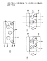
図8(A)は、図6の構成において、複数の色素A,Bを液晶の液滴2中に導入したもので、色素Aと色素Bとは互いに異なった液滴2または2’中に凝集する。ただし、図8(A)中、先に説明した部分には同一の参照符号を付し、説明を省略する。
【0066】
図8(A)を参照するに、色素Aを含む液滴2と色素Bを含む液滴2’とでは、液滴形状の違いに起因してVーT特性が異なっており、このため、駆動電圧範囲を選択することにより、色素Bを含む液滴を2’、色素Aを含む液滴2に対して別個に駆動することが可能である。
【0067】
図8(B)は、高分子マトリクス3中に画成された画素内において、色素Aを含む液滴2の領域と色素Bを含む液滴2’の領域とを分離させた構成を示す。かかる構成は、空の液晶パネルへのプレミクスチャの注入の順序を、所定の順序でくりかえし行うことで得られ、カラー表示に有効である。
【0068】
また、図8(C)は、基板1Aと1Bとの間に挟持された高分子マトリクス3中において、色素Aを含む液滴2と色素Bを含む液滴2’とが、別々の層に含まれている。
[実施例9]
以上は、高分子分散型液晶についての説明であったが、先にも説明したように、本発明は他の液晶表示装置、例えばPSCT液晶を使った液晶表示装置に対しても有用である。
【0069】
例えば、液晶E48(メルク製)を60% カイラル剤CE2(メルク製)を20%、カイラル剤CB15(メルク製)を20%の割合で、120°Cで混合し、液晶混合物4gを作製した。これに、光硬化性樹脂UV10(メルク製)を80:20の割合で混合し、5gのプレミクスチャを形成した。さらに、得られたプレミクスチャに色素SI−497(三井東圧製)を2%加え、十分に攪拌した。
【0070】
攪拌後、得られたプレミクスチャを、透明電極1a,1bを担持する基板1A,1Bを10μmの径のスペーサ(積水ファインケミカル製)を介在して接合して形成した空の液晶パネルに、毛管現象により注入し、液晶パネルを形成した。さらに、プレミクスチャを注入された液晶パネルを70°Cの温度に保持し、色素の吸収波長(500nm〜760nm)をカットした照射光を、30mW/cm2の光量で10分間照射した。照射光は、高圧水銀ランプの光を図7(D)に示す特性の多層膜フィルタで濾波して得た。このようにして得られたPSCT液晶パネルは、電圧無印加時にはシアンを呈し、また5Vの矩形波を印加した場合にコントラスト比として10が得られることが確認された。
[実施例10]
本発明により得られる液晶パネルは、良好な散乱性を示すのみならず、低い駆動電圧で駆動が可能であり、このため、TFTを使ったアクティブマトリクス駆動方式の液晶表示装置に特に有効である。
【0071】
図9は、かかるアクティブマトリクス駆動方式の反射型液晶表示装置の構成を示す図である。
【0072】
図9を参照するに、基板1Aの下にはレンチキュラー板1Dを介して光吸収層1Cが配設され、さらに透明電極層1aは複数の画素電極1a1,1a2,・・・にパターニングされている。さらに、基板1A上には複数の行バスB1,B2、・・・および列バスC1,・・・が縦横に走り、各交点に対応して薄膜トランジスタTFTが形成される。かかる構成では、基板1Bの側には光を遮断する要素は設けられず、TFTを介した各画素電極の駆動により、液晶液滴2の透過・散乱が制御される。ただし、透過型の液晶表示装置の場合には、レンチキュラー板あるいは光吸収層は設けられない。
【0073】
以上の各実施例の照射工程において、光学多層膜フィルタ23(図1)あるいは光学多層膜ミラー23’(図5)は一般に入射角依存性を示すため、光源21は照射光を平行光ビームの形で照射するものであるのが好ましく、光学多層膜フィルタに光ビームを入射させる場合、入射角は0°±10°の範囲に制御するのが好ましい。
【発明の効果】
【0074】
本発明の一の特徴によれば、光硬化性樹脂と液晶とよりなるプレミクスチャの光重合の際に、赤外域を除いた所定の波長領域の光波長成分を照射することにより、プレミクスチャの昇温に伴う液晶の劣化を回避でき、また、複数の光波長成分を照射することにより、十分な光量が得られ、分散性および光散乱性に優れ、高いコントラスト比の表示が可能で、しかもTFTによる低い駆動電圧での駆動が可能な高分子分散型液晶パネルを得ることができる。
【0075】
本発明の他の特徴によれば、光重合工程で使われる赤外域をカットした、しかも所定の範囲の波長領域をカバーする照射光を、容易に得ることができる。
【0076】
本発明の他の特徴によれば、光重合工程において十分な光量の照射光を照射することにより、早い硬化速度と十分な重合反応が得られ、良好な分散性を有し、しかも特性の温度依存性が少ない高分子分散型液晶パネルを得ることができる。
【0077】
本発明の他の特徴によれば、光重合工程で、添加された色素の波長を避けて光照射を行うことにより、色素の劣化の少ない高分子分散型液晶パネルを得ることができる。
【図面の簡単な説明】
【図1】本発明による光重合工程を示す図である。
【図2】図1の工程で使われる光フィルタの特性を示す図である。
【図3】図2のフィルタを使った光重合工程におけるプレミクスチャの昇温を従来の場合と比較して示す図である。
【図4】本発明の一実施例による液晶パネルの構成を示す図である。
【図5】本発明による光重合工程の別の例を示す図である。
【図6】本発明の別の実施例によるよる液晶パネルの構成を示す図である。
【図7】本発明の光重合工程で使われる照射光のスペクトルを説明する図である。
【図8】本発明の別の実施例による液晶パネルの構成を示す図である。
【図9】本発明の別の実施例による液晶パネルの構成を示す図である。
【図10】従来の高分子分散型液晶パネルの構成および動作を説明する図である。
【図11】従来の高分子分散型液晶パネルの別の例を示す図である。
【図12】従来の光重合過程を伴う液晶パネルの製造工程を示す図である。
【図13】光重合過程による高分子分散型液晶パネルの形成過程を説明する図である。
【図14】従来の高分子分散型液晶表示装置の動作特性およびその測定系の構成を説明する図である。
【図15】従来の光重合過程を伴う液晶パネルの製造工程で使われている光開始剤の吸収特性を示す図である。
【図16】従来の光重合過程を伴う液晶パネルの製造工程で使われている高圧水銀ランプの発光スペクトルを示す図である。
【符号の説明】
1 液晶分子
1’ 色素
1A,1B 基板
1C 光吸収層
1D レンチキュラー板
1a,1b 透明電極
1a’,1b’ ポリビニルアルコール層
2,2’ 液晶液滴
3 高分子マトリクス
3A 高分子領域
3B 高分子3次元ネットワーク
3C プレミクスチャ
10,21 光源
11 ディテクタ
22 水銀ランプ
23 光多層膜フィルタ
23’光多層膜ミラー
TFT 薄膜トランジスタ[0001]
BACKGROUND OF THE INVENTION
[0002]
The present invention generally relates to a liquid crystal display device and a method for manufacturing the same, and more particularly to a so-called polymer dispersion type liquid crystal display device or polymer formed by polymerizing and curing a resin by irradiating a mixture of a photocurable resin and a liquid crystal. The present invention relates to a stabilized cholesteric texture (PSCT) liquid crystal display device.
[0003]
A liquid crystal display device has excellent features in terms of low power consumption, thinness, and portability, and is widely used for portable information terminals and the like. In such a portable information terminal, a low power consumption reflective liquid crystal display device that does not require a backlight is particularly desirable.
[Prior art]
[0004]
A polymer dispersed liquid crystal display device or a polymer stabilized cholesteric texture (PSCT) liquid crystal cover device is particularly suitable for a reflective liquid crystal display device having such desirable characteristics, and extensive research and development efforts have been made. ing.
[0005]
The polymer-dispersed liquid crystal panel has a structure in which droplets of liquid crystal molecules are dispersed in a polymer matrix, and has a structure shown in FIG. 10A, for example.
[0006]
Referring to FIG. 10A, the
[0007]
FIG. 10B shows a state in which no electric field is applied between the electrodes 1a and 1b. In this state, it can be seen that the
[0008]
On the other hand, when an electric field is applied between the electrodes 1a and 1b, the
[0009]
In the polymer dispersion type liquid crystal display device, the state of the liquid crystal is not limited to the droplet shape shown in FIG. 10, but the
[0010]
On the other hand, in a PSCT liquid crystal display device using a polymer-stabilized cholesteric texture, display is performed using selective reflection of cholesteric liquid crystal. See, for example, D. K. Yang, SID '92 DIGEST p.759 and J. L. West, SID, '94 DIGEST, p.608. The PSCT liquid crystal display device has excellent reflection characteristics, but may exhibit color. For example, when the whole is greenish, a dye is added to the PSCT layer in order to perform true black-and-white display.
[0011]
In the production of polymer dispersion type liquid crystal display devices, impregnation method, emulsification method, solvent volatilization method, phase separation method and the like are known, but in order to produce a liquid crystal display device with strong light scattering and low driving voltage. A phase separation method using photopolymerization is suitable.
[0012]
12A to 12C are diagrams showing a manufacturing process of a polymer dispersion type liquid crystal display device by a phase separation method using photopolymerization.
[0013]
Referring to FIG. 12A, a liquid crystal and a photocurable resin are mixed to form a uniform mixture (premixture).
[0014]
Next, in the step of FIG. 12 (B), the premixture is injected into the gap between the substrates 1A and 1B superimposed via the seal S, and the
[0015]
Further, in the step of FIG. 12 (C), the injected
[0016]
FIG. 13 shows the polymerization, phase separation and process that occur in the process of FIG.AndIt is a figure which shows formation of a polymer dispersion type liquid crystal scattering layer in the form of a flowchart.
[0017]
Referring to FIG. 13, in step S1, the photocurable resin constituting the
[0018]
FIG. 14A shows the voltage-transmittance curve (VT curve) of the polymer dispersion type liquid crystal display device thus obtained, and FIG. 14B shows the VT curve. The configuration of the evaluation system is shown.
[0019]
Referring to FIG. 14B, the light beam formed by the
[0020]
Referring to FIG. 14A, it can be seen that when the applied voltage V is zero, the scattering of incident light is maximized and the transmittance is the minimum value T0. In other words, T0 represents scattering, and the smaller T0, the better the scattering. On the other hand, when the applied voltage is increased, as described in FIG. 10C, the director of the
[0021]
In the liquid crystal display device, in order to perform a clear display with high contrast, the minimum value T0Is preferably as small as possible. In particular, in a display device driven by an active driving device using TFTs, it is preferable that the transmittance reaches the saturation value Tsat with a driving voltage as low as possible.
[0022]
The scattering property T0 and saturation driving voltage of the polymer-dispersed liquid crystal display device are determined by the dispersibility of the
[0023]
FIG. 15 is a diagram showing the light absorption characteristics of a typical photoinitiator (Irgacure) contained in the photocurable resin, and FIG. 16 shows the spectrum of a lamp used as a light source during the light irradiation process. .
[0024]
Referring to FIG. 15, the initiator absorbs the spectral components from the lamp to generate radicals, and the reaction starts. The reaction is almost free of radicalsMaContinue on.
[Problems to be solved by the invention]
[0025]
However, in the light irradiation process using a light source such as a high-pressure mercury lamp, the temperature of the liquid crystal panel after irradiation increases as the light irradiation intensity increases, and the temperature increases more as the irradiation amount, that is, the irradiation time becomes longer. Problems arise. As a result, the stronger scattering T0However, the
[0026]
As a method for solving this problem, a method is known in which a light beam emitted from a light source is passed through an optical bandpass filter to extract and irradiate a specific single light wavelength component (Japanese Patent Laid-Open No. 5-181118). In this method, a single light wavelength component having a wavelength in the range of ± 20 nm including the absorption peak of the photoinitiator added in the photocurable resin is extracted by a filter and irradiated to the premixture. In particular, light wavelength components corresponding to Hg h-rays in the range of 380 nm to 420 nm are used. On the other hand, even if the wavelength component corresponding to the absorption peak of the photoinitiator is extracted, the light intensity obtained is insufficient, and the dispersibility and thus the scattering property of the obtained liquid crystal panel are unsatisfactory. In addition, the polymerization of the resin forming the polymer matrix is insufficient, and the problem of state change due to temperature or the like and the problem of hysteresis appear remarkably.
[0027]
In summary, in the photopolymerization process of the premixture, even if light obtained from a light source such as a high-pressure mercury lamp is irradiated as it is, strong dispersion cannot be maintained in the polymer dispersion type liquid crystal display device. A contrast cannot be obtained. In addition, even if a specific single light wavelength component is selected and irradiated so as not to cause a temperature rise, a sufficient amount of light cannot be obtained, and the phase separation process such as the curing rate of the resin cannot be sufficiently controlled, As a result, the electro-optical characteristics of the obtained liquid crystal display device must be temperature dependent. Furthermore, in a polymer dispersion type liquid crystal display device, a dichroic dye may be added to liquid crystal droplets to cause color display. In such a case, the dye is irradiated in the photopolymerization process. There is a possibility of deterioration due to light. Similarly, the problem of dye deterioration in the photopolymerization process of the premix occurs not only in the polymer dispersion type liquid crystal display device but also in the PSCT liquid crystal display device.
[0028]
Therefore, the present invention irradiates a pre-mixture composed of a liquid crystal and a photo-curable resin with a light wavelength component of a limited range of wavelengths while excluding the influence of heat and with a sufficient amount of light, and has high scattering properties. Provided are a manufacturing method for manufacturing a polymer dispersed liquid crystal display device having a low drive voltage capable of being displayed with a large contrast and driven by a TFT, and a polymer dispersed liquid crystal display device manufactured by such a manufacturing method. One purpose.
[0029]
Another object of the present invention is to irradiate a premixture composed of a liquid crystal and a photocurable resin with a light wavelength component in a limited range while avoiding the absorption wavelength of the dye added to the liquid crystal. It is an object of the present invention to provide a method of manufacturing a liquid crystal display device that avoids deterioration and such a liquid crystal display device. Such liquid crystal display devices include not only polymer dispersed liquid crystal display devices but also PSCT liquid crystal display devices or other liquid crystal display devices.
[Means for Solving the Problems]
[0030]
The present invention solves the above problems.
As described in
A step of introducing a mixture of a photocurable resin and a liquid crystal between a pair of substrates, and a resin layer formed by curing the photocurable resin by irradiating the mixture with light and curing the photocurable resin. In a method for manufacturing a liquid crystal display device, comprising a step of forming liquid crystal droplets or a continuous layer of liquid crystal by phase separation,
The step of performing the light irradiation is executed by a plurality of light wavelength components in a wavelength region obtained by removing the wavelength in the infrared region by an optical filter,
The step of performing the light irradiation includes at least two of i-line, h-line, and g-line of a high-pressure mercury lamp.book ofLight wavelength componentWithExecuted,
The step of irradiating the light is performed by a light wavelength component in a wavelength region that does not cause a temperature rise of the resin layer, or by a method for manufacturing a liquid crystal display device,
As described in
The method according to
As described in
The step of performing the light irradiation is performed such that the total amount of light wavelength components to be irradiated is 600 mJ or more.2Or a liquid crystal display device manufacturing method according to any one of
As described in
The said liquid crystal contains a pigment | dye and the process of performing the said light irradiation is performed by the light wavelength component which avoided the wavelength range which the said pigment | dye absorbs.3Or a liquid crystal display device manufacturing method according to any one of
As described in
The step of performing the light irradiation is performed by cutting a wavelength component that degrades the pigment.4According to the manufacturing method of the liquid crystal display device described, or
As described in
The step of performing the light irradiation is performed by maintaining the temperature of the mixture at a predetermined temperature higher than room temperature, and the liquid crystal has a polymer-stabilized cholesteric texture in the cured resin layer.
[0031]
In the present invention, when producing a polymer-dispersed liquid crystal display device, in the step of irradiating light, an infrared wavelength component that filters the light beam emitted from the light source through an optical filter and raises the temperature of the premixture. And a plurality of emission line wavelengths corresponding to the absorption wavelength of the photoinitiator added to the premixture are extracted and irradiated to the premixture. Since a plurality of bright line wavelengths excluding the infrared region are used, the temperature rise is suppressed, and at the same time, the amount of light irradiation is increased and the initial curing rate is increased. As a result, the dispersibility of the liquid crystal in the cured polymer matrix is improved, and the scattering T0As a result, a high contrast display can be obtained. In addition, driving with a low driving voltage is possible. Further, as a result of using a plurality of emission line wavelengths, the amount of light irradiation increases, the polymerization of the photocurable resin in the premixture proceeds sufficiently, and problems such as the appearance of hysteresis in VT characteristics are solved.
[0032]
Further, in a liquid crystal display device using a liquid crystal to which a dye is added, light irradiation is performed while avoiding the absorption wavelength of the dye, so that the dye does not deteriorate.
DETAILED DESCRIPTION OF THE INVENTION
[0033]
Hereinafter, the present invention will be described in detail with reference to examples.
[0034]
FIG. 1 is a diagram for explaining a light irradiation process according to an embodiment of the present invention corresponding to the process of FIG.
[0035]
Referring to FIG. 1, a parallel light beam formed by a
[0036]
Hereinafter, an experimental example in which photopolymerization is performed with the configuration of FIG. 1 will be described in detail.
[Example 1]
Liquid crystal TL205 (manufactured by Merck) and photocurable resin PN393 (manufactured by Merck) were mixed at a weight ratio of 4: 1 and stirred to prepare a premix.
[0037]
Further, microbar spacers (SP10100 made by Sekisui Fine Chemical) were sprayed on a glass substrate 1 (OA2 made by Nippon Electric Glass) on which an ITO layer was formed as the transparent electrode 1a, and a seal S was formed with a thermosetting resin. Further, a similar glass substrate 1B on which an ITO film acting as a transparent electrode 1b is formed is disposed on the substrate 1A so that the surfaces on which the electrodes 1a and 1b are formed face each other, and are adhered at the seal S to adhere to the cell. An empty panel having a thickness of 10 μm was formed.
[0038]
Furthermore, the above-mentioned premixture was injected into the empty panel thus formed by capillary action to form a
[0039]
[Table 1]
[0040]
In Table 1, the stage indicated as “Example 1” indicates the scattering property T of the liquid crystal panel thus obtained.0(The light transmittance when the capture angle θ is 12 ° and the drive voltage is 0V) and the contrast ratio when the drive voltage is 7V, when light irradiation is performed without a filter, only the Hg i-line (365 nm) When using Hg, using only Hg line (405 nm), using only Hg gline (436 nm), using Hg i line and h line , Hg h line and g line are used, and Hg i line, h line, and g line are used. However, in each stage of Table 1, the upper stage is scattering T0The lower end indicates the contrast ratio.
[0041]
As can be seen from Table 1, the scattering is improved when irradiation is performed using a plurality of bright lines compared to the case where no filter is used or only a single bright line is used. The ratio has improved.
[0042]
When a polymer dispersed liquid crystal panel obtained by irradiating a plurality of bright lines is observed with a laser microscope (made by Lasertec), the diameter of the
[0043]
FIG. 3 shows the results of measuring the temperature rise of the premix for the composition of Example 1 when no filter is used and when infrared radiation is cut using the filter.
[0044]
Referring to FIG. 3, when no filter is used, even if there is no main Hg emission line in the infrared region, the temperature of the premixture exceeds 100 ° C. several minutes after the start of irradiation, and phase separation occurs. It can be seen that the state and other morphologies are degraded. On the other hand, if the wavelength in the infrared region is cut with a filter, it is understood that the temperature rise of the premix does not substantially occur.
[Example 2]
A liquid crystal TL205 (manufactured by Merck) and a photocurable resin A (manufactured by Nippon Kayaku Co., Ltd.) made of an epoxy acrylate were mixed at a weight ratio of 7: 3 and stirred to prepare a premixture. Furthermore, Irgacure 184 (manufactured by Ciba Geigy) was mixed as a photoinitiator at a ratio of 2 percent by weight with respect to the resin.
[0045]
Further, as in the case of Example 1, microbar spacers (SP10100 made by Sekisui Fine Chemical) were sprayed on the glass substrate 1 (OA2 made by Nippon Electric Glass) on which the ITO layer was formed as the transparent electrode 1a, and thermosetting was performed. The seal S was formed with a functional resin. Further, a similar glass substrate 1B on which an ITO film acting as a transparent electrode 1b is formed is disposed on the substrate 1A so that the surfaces on which the electrodes 1a and 1b are formed face each other, and are adhered at the seal S to adhere to the cell. An empty panel having a thickness of 10 μm was formed.
[0046]
Further, the above premixture was injected into the empty panel formed in this way by a vacuum injection method to form a
[0047]
The stage shown as “Example 2” in Table 1 shows the scattering T of the liquid crystal panel thus obtained.0(The light transmittance when the capture angle θ is 12 ° and the drive voltage is 0V) and the contrast ratio when the drive voltage is 7V, when light irradiation is performed without a filter, only the Hg i-line (365 nm) When using Hg, using only Hg line (405 nm), using only Hg gline (436 nm), using Hg i line and h line , Hg h line and g line are used, and Hg i line, h line, and g line are used. As is clear from Table 1, also in Example 2, the scattering T is more effective when irradiation is performed using a plurality of bright lines than when no filter is used or only a single bright line is used.0Therefore, the contrast ratio is improved. Further, in this example, there is no resin dependency as compared with Example 1.
[Example 3]
Liquid crystal TL205 (made by Merck) and photocurable resin B (made by Nippon Kayaku) made of urethane acrylate were mixed at a weight ratio of 7: 3 and stirred to prepare a premixture. Furthermore, Irgacure 184 (manufactured by Ciba Geigy) was mixed as a photoinitiator at a ratio of 2 percent by weight with respect to the resin.
[0048]
Further, as in the case of Examples 1 and 2, a microbar spacer (SP10100 made by Sekisui Fine Chemical) was sprayed on a glass substrate 1 (OA2 made by Nippon Electric Glass) on which an ITO layer was formed as the transparent electrode 1a. A seal S was formed with a thermosetting resin. Further, a similar glass substrate 1B on which an ITO film acting as a transparent electrode 1b is formed is disposed on the substrate 1A so that the surfaces on which the electrodes 1a and 1b are formed face each other, and are adhered at the seal S to adhere to the cell. An empty panel having a thickness of 10 μm was formed.
[0049]
Further, the above premixture was injected into the empty panel formed in this way by a vacuum injection method to form a
[0050]
The stage shown as “Example 3” in Table 1 shows the scattering T of the liquid crystal panel thus obtained.0(The light transmittance when the capture angle θ is 12 ° and the drive voltage is 0V) and the contrast ratio when the drive voltage is 7V, when light irradiation is performed without a filter, only the Hg i-line (365 nm) When using Hg, using only Hg line (405 nm), using only Hg gline (436 nm), using Hg i line and h line , Hg h line and g line are used, and Hg i line, h line, and g line are used. As is clear from Table 1, the examples3However, in the case of irradiating with a plurality of emission lines, the scattering T is greater than when no filter is used or only a single emission line is used.0Therefore, the contrast ratio is improved. In this embodiment, there is no material dependency such as a liquid crystal material or a photocurable resin.
[0051]
As can be seen from Table 1, also in this example, by performing photopolymerization using a plurality of bright lines, it is possible to scatter without using a filter or by performing photopolymerization using only a single bright line. T0The contrast ratio is improved. The same effect can be obtained when an additive such as a dispersant is included.
[Example 5]
Similar to Example 1, liquid crystal 205 (Merck) and photo-curing resin (Merck) were mixed and stirred at a weight ratio of 4: 1 to form a premixture. Injected into the panel. At that time, as shown in FIG. 4, on the opposite surfaces of the substrates 1A and 1B constituting the liquid crystal panel, the thin films 1a ′ and 1b ′ of polyvinyl alcohol (made by Kuraray) are formed on the transparent electrode layers 1a and 1b. Were formed with a thickness of 60 nm. Furthermore, a multilayer film filter (manufactured by Asahi Spectroscope) with various transmission characteristics is placed on the liquid crystal panel thus formed, and a high-pressure mercury lamp (Oak Seisakusho, H series) is used in the same manner as in the previous embodiment. Irradiation was performed for 3 minutes.
[0052]
As can be seen from Table 1, also in this example, by performing photopolymerization using a plurality of bright lines, it is possible to scatter without using a filter or by performing photopolymerization using only a single bright line. T0The contrast ratio is improved.
[Example 6]
Furthermore, the filter used when filtering the light from the light source is not limited to the multilayer filter, and may be, for example, a multilayer mirror that reflects a specific wavelength and transmits infrared rays.
[0053]
FIG. 5 shows an example in which such a
[0054]
[Table 2]
[0055]
Referring to Table 2, as compared with the case where the light from the
[Example 7]
By the way, when performing color display in a reflective liquid crystal display device using a polymer dispersed liquid crystal, a dye or a dye is added to the liquid crystal. In the production of such a color polymer dispersed liquid crystal panel. In particular, in the photopolymerization step, it is necessary to prevent deterioration of the pigment or dye added to the liquid crystal.
[0056]
FIG. 6 shows the structure of such a polymer dispersed liquid crystal panel to which a dye is added. However, in FIG. 6, the parts described above are denoted by corresponding reference numerals, and description thereof is omitted.
[0057]
Referring to FIG. 6, a light absorbing plate 1C is provided under the substrate 1A, and a lenticular plate 1D is further provided between the substrate 1A and the light absorbing plate 1C. However, the lenticular plate 1D may be omitted. In the liquid crystal,
[0058]
The
[0059]
FIG. 7 (A) corresponds to FIG. 16 and shows the light spectrum formed by the high pressure mercury lamp, while FIG. 7 (B) corresponds to FIG. 15 and shows the absorption spectrum of a typical photoinitiator. . FIG. 7C shows a typical absorption spectrum of a cyan dye added to the liquid crystal.
[0060]
Referring to FIGS. 7A to 7C, the photoinitiator has an absorption band at a wavelength of 600 nm or less, whereas the dye has an absorption band at a wavelength of 500 nm or more. Is filtered at a wavelength of 600 nm or less in accordance with the absorption band of the photoinitiator, an overlap with the absorption wavelength of the dye occurs in the range of 500 nm to 600 nm. In other words, there is a possibility that the dye 1 'is irradiated with strong irradiation light in this wavelength range and deteriorated.
[0061]
Therefore, in the present invention, the characteristics of the
[0062]
As an example, an epoxy acrylate oligomer (manufactured by Nippon Kayaku) in which liquid crystal TL205 (manufactured by Merck) and ultraviolet curable resin A (manufactured by Nippon Kayaku) are diluted with 2-ethylhexyl acrylate (manufactured by Nippon Kayaku) In a weight ratio of 75:25. Further, the ultraviolet curable resin A contained Irgacure 184 (manufactured by Ciba Geigy) as a photopolymerization initiator in a proportion of 2% by weight with respect to the resin. Further, a dichroic dye SI-497 (manufactured by Mitsui Toatsu) was further added to the mixture of liquid crystal and resin thus obtained to form a premixture.
[0063]
Further, the thus obtained premixture was injected by capillary action into an empty liquid crystal panel formed by bonding the substrates 1A and 1B with a 12 μm diameter spacer (manufactured by Sekisui Fine Chemical).
[0064]
After injection, with respect to the premixture in the liquid crystal panel, avoiding the dye absorption wavelength band (500 nm to 760 nm), the irradiation light with a wavelength of 450 nm is 30 mW / cm.2Irradiated at an intensity of 5 minutes. Irradiation light was obtained by filtering the light formed by the high-pressure mercury lamp 21 (FIG. 1) with a multilayer filter 23 (manufactured by Kenko) having the characteristics shown in FIG. 7D.
[0065]
According to such a configuration, since the dye is not deteriorated, a color reflective liquid crystal display device having good dichroism, good scattering properties, and a high contrast ratio can be obtained. As can be seen from the characteristics of FIG. 7D, the filter used in this example also cuts infrared radiation, and the resulting liquid crystal panel is not deteriorated by heat. In addition, since ultraviolet rays having a short wavelength are also cut, deterioration of the liquid crystal itself can be prevented. Furthermore, since the
[Example 8]
FIG. 8A shows a structure in which a plurality of dyes A and B are introduced into the
[0066]
Referring to FIG. 8A, the
[0067]
FIG. 8B shows a configuration in which the region of the
[0068]
Further, FIG. 8C shows that in the
[Example 9]
The above is a description of the polymer dispersed liquid crystal, but as described above, the present invention is also useful for other liquid crystal display devices, for example, liquid crystal display devices using PSCT liquid crystal.
[0069]
For example, liquid crystal E48 (manufactured by Merck) was mixed with 60% chiral agent CE2 (manufactured by Merck) at 20% and chiral agent CB15 (manufactured by Merck) at a ratio of 20% at 120 ° C. to prepare 4 g of a liquid crystal mixture. This was mixed with a photocurable resin UV10 (manufactured by Merck) at a ratio of 80:20 to form a 5 g premixture. Furthermore, 2% of dye SI-497 (manufactured by Mitsui Toatsu) was added to the obtained premixture, and the mixture was sufficiently stirred.
[0070]
After stirring, the obtained premixture was subjected to capillary action on an empty liquid crystal panel formed by joining the substrates 1A and 1B carrying the transparent electrodes 1a and 1b with a spacer having a diameter of 10 μm (manufactured by Sekisui Fine Chemical). Was injected to form a liquid crystal panel. Furthermore, the liquid crystal panel in which the premixture was injected was kept at a temperature of 70 ° C., and the irradiation light with the absorption wavelength (500 nm to 760 nm) of the dye cut was reduced to 30 mW / cm.2For 10 minutes. Irradiation light was obtained by filtering light from a high-pressure mercury lamp through a multilayer filter having the characteristics shown in FIG. It was confirmed that the PSCT liquid crystal panel thus obtained exhibited cyan when no voltage was applied, and that a contrast ratio of 10 was obtained when a 5 V rectangular wave was applied.
[Example 10]
The liquid crystal panel obtained by the present invention not only exhibits good scattering properties but also can be driven with a low driving voltage, and is therefore particularly effective for an active matrix liquid crystal display device using TFTs.
[0071]
FIG. 9 is a diagram showing the configuration of such an active matrix drive type reflective liquid crystal display device.
[0072]
Referring to FIG. 9, a light absorption layer 1C is disposed under a substrate 1A via a lenticular plate 1D, and the transparent electrode layer 1a is composed of a plurality of pixel electrodes 1a.1, 1a2, ... are patterned. Further, a plurality of row buses B are provided on the substrate 1A.1, B2, ... and column bus C1,... Run vertically and horizontally, and a thin film transistor TFT is formed corresponding to each intersection. In such a configuration, an element for blocking light is not provided on the substrate 1B side, and transmission / scattering of the
[0073]
In the irradiation process of each of the above embodiments, the optical multilayer filter 23 (FIG. 1) or the
【The invention's effect】
[0074]
One of the present inventionAccording to the feature, the liquid crystal accompanying the temperature increase of the premixture by irradiating the light wavelength component in the predetermined wavelength region excluding the infrared region during the photopolymerization of the premixture composed of the photocurable resin and the liquid crystal. In addition, by irradiating multiple light wavelength components, a sufficient amount of light can be obtained, it is excellent in dispersibility and light scattering, a high contrast ratio display is possible, and a low drive voltage by TFT A polymer-dispersed liquid crystal panel that can be driven at a low temperature can be obtained.
[0075]
Other of the present inventionAccording to the feature, it is possible to easily obtain irradiation light that cuts the infrared region used in the photopolymerization step and covers a predetermined wavelength range.
[0076]
Other of the present inventionAccording to the characteristics, by irradiating with a sufficient amount of irradiation light in the photopolymerization process, a high curing speed and a sufficient polymerization reaction can be obtained, it has good dispersibility, and the temperature dependence of the characteristics is low. A molecular dispersion type liquid crystal panel can be obtained.
[0077]
Other of the present inventionAccording to the feature, a polymer-dispersed liquid crystal panel with little deterioration of the dye can be obtained by performing light irradiation in the photopolymerization step while avoiding the wavelength of the added dye.
[Brief description of the drawings]
FIG. 1 shows a photopolymerization process according to the present invention.
FIG. 2 is a diagram showing characteristics of an optical filter used in the process of FIG.
FIG. 3 is a diagram showing a temperature increase of a premix in a photopolymerization process using the filter of FIG. 2 in comparison with a conventional case.
FIG. 4 is a diagram illustrating a configuration of a liquid crystal panel according to an embodiment of the present invention.
FIG. 5 is a diagram showing another example of the photopolymerization step according to the present invention.
FIG. 6 is a diagram showing a configuration of a liquid crystal panel according to another embodiment of the present invention.
FIG. 7 is a diagram for explaining the spectrum of irradiation light used in the photopolymerization step of the present invention.
FIG. 8 is a diagram showing a configuration of a liquid crystal panel according to another embodiment of the present invention.
FIG. 9 is a diagram showing a configuration of a liquid crystal panel according to another embodiment of the present invention.
FIG. 10 is a diagram for explaining the configuration and operation of a conventional polymer-dispersed liquid crystal panel.
FIG. 11 is a diagram showing another example of a conventional polymer-dispersed liquid crystal panel.
FIG. 12 is a view showing a manufacturing process of a liquid crystal panel with a conventional photopolymerization process.
FIG. 13 is a diagram illustrating a process of forming a polymer dispersion type liquid crystal panel by a photopolymerization process.
FIG. 14 is a diagram for explaining the operational characteristics of a conventional polymer-dispersed liquid crystal display device and the configuration of its measurement system.
FIG. 15 is a graph showing absorption characteristics of a photoinitiator used in a manufacturing process of a liquid crystal panel involving a conventional photopolymerization process.
FIG. 16 is a diagram showing an emission spectrum of a high-pressure mercury lamp used in a liquid crystal panel manufacturing process involving a conventional photopolymerization process.
[Explanation of symbols]
1 Liquid crystal molecules
1 'dye
1A, 1B substrate
1C Light absorption layer
1D lenticular plate
1a, 1b Transparent electrode
1a ', 1b' polyvinyl alcohol layer
2,2 'liquid crystal droplets
3 Polymer matrix
3A Polymer area
3B 3D polymer network
3C premixture
10, 21 Light source
11 Detector
22 Mercury lamp
23 Optical multilayer filter
23 'optical multilayer mirror
TFT Thin film transistor
Claims (6)
前記光照射を行う工程は、赤外域の波長を、光フィルタにより除いた波長領域の複数の光波長成分により実行され、
前記光照射を行う工程は、高圧水銀ランプのi線,h線,g線のうち少なくとも2本の光波長成分を使って実行され、
前記光照射を行う工程は、前記樹脂層の昇温が生じないような波長領域の光波長成分により実行されることを特徴とする液晶表示装置の製造方法。A step of introducing a mixture of a photocurable resin and a liquid crystal between a pair of substrates; and a resin layer formed by curing the photocurable resin by irradiating the mixture with light and curing the photocurable resin. In a method for manufacturing a liquid crystal display device, comprising a step of forming liquid crystal droplets or a continuous layer of liquid crystal by phase separation,
The step of performing the light irradiation is executed by a plurality of light wavelength components in a wavelength region obtained by removing the wavelength in the infrared region by an optical filter,
Step of performing the light irradiation, i-ray of a high-pressure mercury lamp, h line, using at least two light wavelength components of the g-line is executed,
The method of manufacturing a liquid crystal display device, wherein the step of irradiating the light is performed by a light wavelength component in a wavelength region that does not cause a temperature rise of the resin layer.
Priority Applications (1)
| Application Number | Priority Date | Filing Date | Title |
|---|---|---|---|
| JP27314095A JP3981164B2 (en) | 1995-10-20 | 1995-10-20 | Manufacturing method of liquid crystal display device |
Applications Claiming Priority (1)
| Application Number | Priority Date | Filing Date | Title |
|---|---|---|---|
| JP27314095A JP3981164B2 (en) | 1995-10-20 | 1995-10-20 | Manufacturing method of liquid crystal display device |
Publications (2)
| Publication Number | Publication Date |
|---|---|
| JPH09113881A JPH09113881A (en) | 1997-05-02 |
| JP3981164B2 true JP3981164B2 (en) | 2007-09-26 |
Family
ID=17523682
Family Applications (1)
| Application Number | Title | Priority Date | Filing Date |
|---|---|---|---|
| JP27314095A Expired - Fee Related JP3981164B2 (en) | 1995-10-20 | 1995-10-20 | Manufacturing method of liquid crystal display device |
Country Status (1)
| Country | Link |
|---|---|
| JP (1) | JP3981164B2 (en) |
Families Citing this family (5)
| Publication number | Priority date | Publication date | Assignee | Title |
|---|---|---|---|---|
| JP4703045B2 (en) * | 2001-07-10 | 2011-06-15 | 大日本印刷株式会社 | Manufacturing method of color filter |
| JP4703048B2 (en) * | 2001-07-17 | 2011-06-15 | 大日本印刷株式会社 | Manufacturing method of color filter |
| US20090316060A1 (en) | 2008-06-18 | 2009-12-24 | 3M Innovative Properties Company | Conducting film or electrode with improved optical and electrical performance |
| US9581870B2 (en) | 2009-08-13 | 2017-02-28 | 3M Innovative Properties Company | Conducting film or electrode with improved optical and electrical performance for display and lighting devices and solar cells |
| TWI591407B (en) * | 2012-03-13 | 2017-07-11 | 半導體能源研究所股份有限公司 | Liquid crystal layer and display device |
-
1995
- 1995-10-20 JP JP27314095A patent/JP3981164B2/en not_active Expired - Fee Related
Also Published As
| Publication number | Publication date |
|---|---|
| JPH09113881A (en) | 1997-05-02 |
Similar Documents
| Publication | Publication Date | Title |
|---|---|---|
| US5771084A (en) | Liquid crystal display device and method for fabricating the same | |
| JP3078623B2 (en) | Liquid crystal electro-optical device and manufacturing method thereof | |
| JP2009075624A (en) | Broadband reflective display device | |
| JPH10222104A (en) | Reflection type display unit using holography | |
| US5576856A (en) | Liquid crystal display device and method for producing the same using photopolymerization with linearly polarized light | |
| Halder et al. | Aligned polymer dispersed liquid crystal film for light enhancement of quantum dot backlight | |
| JP2775769B2 (en) | Projection active matrix liquid crystal display device and method of manufacturing the same | |
| JP3981164B2 (en) | Manufacturing method of liquid crystal display device | |
| JP3370758B2 (en) | Liquid crystal panel, method of manufacturing the same, and projection display device | |
| JP4889643B2 (en) | Optical switch using holographic polymer dispersed liquid crystal | |
| JP3077356B2 (en) | Liquid crystal panel and liquid crystal projection television using the same | |
| JP2870826B2 (en) | Active matrix liquid crystal display device and projection type active matrix liquid crystal display device | |
| JP2778297B2 (en) | Reflective liquid crystal display device and driving method thereof | |
| JPH11125808A (en) | Liquid crystal optical element and its production | |
| JP3864429B2 (en) | LCD device | |
| JPH03276127A (en) | Photoresponsive film and production thereof | |
| JP2792984B2 (en) | Projection type liquid crystal display | |
| JPH05181401A (en) | Production of volumetric hologram optical film, liquid crystal optical element | |
| JP3250836B2 (en) | Liquid crystal panel and projection display device using the liquid crystal panel | |
| JP2796912B2 (en) | Liquid crystal electro-optical device | |
| JP2946538B2 (en) | Projection type active matrix liquid crystal display | |
| JP3345181B2 (en) | Liquid crystal display element and liquid crystal display device | |
| JP2933858B2 (en) | Liquid crystal display device and method of manufacturing the same | |
| JP3315433B2 (en) | Volume hologram optical film, liquid crystal optical element and method of manufacturing the same | |
| JP2000066177A (en) | Method for evaluating light absorption of polymer dispersed liquid crystal, liquid crystal display device and liquid crystal projector |
Legal Events
| Date | Code | Title | Description |
|---|---|---|---|
| A977 | Report on retrieval |
Free format text: JAPANESE INTERMEDIATE CODE: A971007 Effective date: 20031210 |
|
| A131 | Notification of reasons for refusal |
Free format text: JAPANESE INTERMEDIATE CODE: A131 Effective date: 20040224 |
|
| A521 | Request for written amendment filed |
Free format text: JAPANESE INTERMEDIATE CODE: A523 Effective date: 20040423 |
|
| A02 | Decision of refusal |
Free format text: JAPANESE INTERMEDIATE CODE: A02 Effective date: 20040914 |
|
| A521 | Request for written amendment filed |
Free format text: JAPANESE INTERMEDIATE CODE: A523 Effective date: 20041014 |
|
| A911 | Transfer to examiner for re-examination before appeal (zenchi) |
Free format text: JAPANESE INTERMEDIATE CODE: A911 Effective date: 20041122 |
|
| A912 | Re-examination (zenchi) completed and case transferred to appeal board |
Free format text: JAPANESE INTERMEDIATE CODE: A912 Effective date: 20041217 |
|
| A711 | Notification of change in applicant |
Free format text: JAPANESE INTERMEDIATE CODE: A711 Effective date: 20050712 |
|
| A711 | Notification of change in applicant |
Free format text: JAPANESE INTERMEDIATE CODE: A711 Effective date: 20050713 |
|
| RD02 | Notification of acceptance of power of attorney |
Free format text: JAPANESE INTERMEDIATE CODE: A7422 Effective date: 20050722 |
|
| A521 | Request for written amendment filed |
Free format text: JAPANESE INTERMEDIATE CODE: A523 Effective date: 20070531 |
|
| A61 | First payment of annual fees (during grant procedure) |
Free format text: JAPANESE INTERMEDIATE CODE: A61 Effective date: 20070629 |
|
| R150 | Certificate of patent or registration of utility model |
Free format text: JAPANESE INTERMEDIATE CODE: R150 |
|
| FPAY | Renewal fee payment (event date is renewal date of database) |
Free format text: PAYMENT UNTIL: 20100706 Year of fee payment: 3 |
|
| FPAY | Renewal fee payment (event date is renewal date of database) |
Free format text: PAYMENT UNTIL: 20110706 Year of fee payment: 4 |
|
| FPAY | Renewal fee payment (event date is renewal date of database) |
Free format text: PAYMENT UNTIL: 20110706 Year of fee payment: 4 |
|
| FPAY | Renewal fee payment (event date is renewal date of database) |
Free format text: PAYMENT UNTIL: 20120706 Year of fee payment: 5 |
|
| FPAY | Renewal fee payment (event date is renewal date of database) |
Free format text: PAYMENT UNTIL: 20120706 Year of fee payment: 5 |
|
| FPAY | Renewal fee payment (event date is renewal date of database) |
Free format text: PAYMENT UNTIL: 20130706 Year of fee payment: 6 |
|
| LAPS | Cancellation because of no payment of annual fees |