JP3912111B2 - Wavelength multiplexing bidirectional optical transmission module - Google Patents
Wavelength multiplexing bidirectional optical transmission module Download PDFInfo
- Publication number
- JP3912111B2 JP3912111B2 JP2002002784A JP2002002784A JP3912111B2 JP 3912111 B2 JP3912111 B2 JP 3912111B2 JP 2002002784 A JP2002002784 A JP 2002002784A JP 2002002784 A JP2002002784 A JP 2002002784A JP 3912111 B2 JP3912111 B2 JP 3912111B2
- Authority
- JP
- Japan
- Prior art keywords
- wavelength
- light
- transmission module
- diffraction grating
- optical transmission
- Prior art date
- Legal status (The legal status is an assumption and is not a legal conclusion. Google has not performed a legal analysis and makes no representation as to the accuracy of the status listed.)
- Expired - Fee Related
Links
Images


Classifications
-
- G—PHYSICS
- G02—OPTICS
- G02B—OPTICAL ELEMENTS, SYSTEMS OR APPARATUS
- G02B6/00—Light guides; Structural details of arrangements comprising light guides and other optical elements, e.g. couplings
- G02B6/24—Coupling light guides
- G02B6/42—Coupling light guides with opto-electronic elements
- G02B6/4201—Packages, e.g. shape, construction, internal or external details
- G02B6/4246—Bidirectionally operating package structures
-
- G—PHYSICS
- G02—OPTICS
- G02B—OPTICAL ELEMENTS, SYSTEMS OR APPARATUS
- G02B6/00—Light guides; Structural details of arrangements comprising light guides and other optical elements, e.g. couplings
- G02B6/24—Coupling light guides
- G02B6/42—Coupling light guides with opto-electronic elements
- G02B6/4201—Packages, e.g. shape, construction, internal or external details
- G02B6/4219—Mechanical fixtures for holding or positioning the elements relative to each other in the couplings; Alignment methods for the elements, e.g. measuring or observing methods especially used therefor
- G02B6/4236—Fixing or mounting methods of the aligned elements
- G02B6/424—Mounting of the optical light guide
-
- G—PHYSICS
- G02—OPTICS
- G02B—OPTICAL ELEMENTS, SYSTEMS OR APPARATUS
- G02B6/00—Light guides; Structural details of arrangements comprising light guides and other optical elements, e.g. couplings
- G02B6/24—Coupling light guides
- G02B6/42—Coupling light guides with opto-electronic elements
- G02B6/4201—Packages, e.g. shape, construction, internal or external details
- G02B6/4256—Details of housings
- G02B6/4257—Details of housings having a supporting carrier or a mounting substrate or a mounting plate
- G02B6/4259—Details of housings having a supporting carrier or a mounting substrate or a mounting plate of the transparent type
-
- G—PHYSICS
- G02—OPTICS
- G02B—OPTICAL ELEMENTS, SYSTEMS OR APPARATUS
- G02B6/00—Light guides; Structural details of arrangements comprising light guides and other optical elements, e.g. couplings
- G02B6/24—Coupling light guides
- G02B6/42—Coupling light guides with opto-electronic elements
- G02B6/4201—Packages, e.g. shape, construction, internal or external details
- G02B6/4256—Details of housings
- G02B6/4262—Details of housings characterised by the shape of the housing
- G02B6/4263—Details of housings characterised by the shape of the housing of the transisitor outline [TO] can type
-
- G—PHYSICS
- G02—OPTICS
- G02B—OPTICAL ELEMENTS, SYSTEMS OR APPARATUS
- G02B6/00—Light guides; Structural details of arrangements comprising light guides and other optical elements, e.g. couplings
- G02B6/24—Coupling light guides
- G02B6/42—Coupling light guides with opto-electronic elements
- G02B6/4201—Packages, e.g. shape, construction, internal or external details
- G02B6/4286—Optical modules with optical power monitoring
-
- G—PHYSICS
- G02—OPTICS
- G02B—OPTICAL ELEMENTS, SYSTEMS OR APPARATUS
- G02B6/00—Light guides; Structural details of arrangements comprising light guides and other optical elements, e.g. couplings
- G02B6/24—Coupling light guides
- G02B6/42—Coupling light guides with opto-electronic elements
- G02B6/4201—Packages, e.g. shape, construction, internal or external details
- G02B6/4204—Packages, e.g. shape, construction, internal or external details the coupling comprising intermediate optical elements, e.g. lenses, holograms
- G02B6/4215—Packages, e.g. shape, construction, internal or external details the coupling comprising intermediate optical elements, e.g. lenses, holograms the intermediate optical elements being wavelength selective optical elements, e.g. variable wavelength optical modules or wavelength lockers
-
- G—PHYSICS
- G02—OPTICS
- G02B—OPTICAL ELEMENTS, SYSTEMS OR APPARATUS
- G02B6/00—Light guides; Structural details of arrangements comprising light guides and other optical elements, e.g. couplings
- G02B6/24—Coupling light guides
- G02B6/42—Coupling light guides with opto-electronic elements
- G02B6/4201—Packages, e.g. shape, construction, internal or external details
- G02B6/4249—Packages, e.g. shape, construction, internal or external details comprising arrays of active devices and fibres
-
- G—PHYSICS
- G02—OPTICS
- G02B—OPTICAL ELEMENTS, SYSTEMS OR APPARATUS
- G02B6/00—Light guides; Structural details of arrangements comprising light guides and other optical elements, e.g. couplings
- G02B6/24—Coupling light guides
- G02B6/42—Coupling light guides with opto-electronic elements
- G02B6/4201—Packages, e.g. shape, construction, internal or external details
- G02B6/4266—Thermal aspects, temperature control or temperature monitoring
- G02B6/4268—Cooling
- G02B6/4269—Cooling with heat sinks or radiation fins
-
- H—ELECTRICITY
- H01—ELECTRIC ELEMENTS
- H01L—SEMICONDUCTOR DEVICES NOT COVERED BY CLASS H10
- H01L2224/00—Indexing scheme for arrangements for connecting or disconnecting semiconductor or solid-state bodies and methods related thereto as covered by H01L24/00
- H01L2224/01—Means for bonding being attached to, or being formed on, the surface to be connected, e.g. chip-to-package, die-attach, "first-level" interconnects; Manufacturing methods related thereto
- H01L2224/42—Wire connectors; Manufacturing methods related thereto
- H01L2224/44—Structure, shape, material or disposition of the wire connectors prior to the connecting process
- H01L2224/45—Structure, shape, material or disposition of the wire connectors prior to the connecting process of an individual wire connector
- H01L2224/45001—Core members of the connector
- H01L2224/45099—Material
- H01L2224/451—Material with a principal constituent of the material being a metal or a metalloid, e.g. boron (B), silicon (Si), germanium (Ge), arsenic (As), antimony (Sb), tellurium (Te) and polonium (Po), and alloys thereof
- H01L2224/45138—Material with a principal constituent of the material being a metal or a metalloid, e.g. boron (B), silicon (Si), germanium (Ge), arsenic (As), antimony (Sb), tellurium (Te) and polonium (Po), and alloys thereof the principal constituent melting at a temperature of greater than or equal to 950°C and less than 1550°C
- H01L2224/45144—Gold (Au) as principal constituent
-
- H—ELECTRICITY
- H01—ELECTRIC ELEMENTS
- H01L—SEMICONDUCTOR DEVICES NOT COVERED BY CLASS H10
- H01L2224/00—Indexing scheme for arrangements for connecting or disconnecting semiconductor or solid-state bodies and methods related thereto as covered by H01L24/00
- H01L2224/01—Means for bonding being attached to, or being formed on, the surface to be connected, e.g. chip-to-package, die-attach, "first-level" interconnects; Manufacturing methods related thereto
- H01L2224/42—Wire connectors; Manufacturing methods related thereto
- H01L2224/47—Structure, shape, material or disposition of the wire connectors after the connecting process
- H01L2224/48—Structure, shape, material or disposition of the wire connectors after the connecting process of an individual wire connector
- H01L2224/4805—Shape
- H01L2224/4809—Loop shape
- H01L2224/48091—Arched
-
- H—ELECTRICITY
- H01—ELECTRIC ELEMENTS
- H01S—DEVICES USING THE PROCESS OF LIGHT AMPLIFICATION BY STIMULATED EMISSION OF RADIATION [LASER] TO AMPLIFY OR GENERATE LIGHT; DEVICES USING STIMULATED EMISSION OF ELECTROMAGNETIC RADIATION IN WAVE RANGES OTHER THAN OPTICAL
- H01S5/00—Semiconductor lasers
- H01S5/02—Structural details or components not essential to laser action
- H01S5/022—Mountings; Housings
- H01S5/0225—Out-coupling of light
- H01S5/02251—Out-coupling of light using optical fibres
-
- H—ELECTRICITY
- H01—ELECTRIC ELEMENTS
- H01S—DEVICES USING THE PROCESS OF LIGHT AMPLIFICATION BY STIMULATED EMISSION OF RADIATION [LASER] TO AMPLIFY OR GENERATE LIGHT; DEVICES USING STIMULATED EMISSION OF ELECTROMAGNETIC RADIATION IN WAVE RANGES OTHER THAN OPTICAL
- H01S5/00—Semiconductor lasers
- H01S5/02—Structural details or components not essential to laser action
- H01S5/022—Mountings; Housings
- H01S5/0225—Out-coupling of light
- H01S5/02255—Out-coupling of light using beam deflecting elements
-
- H—ELECTRICITY
- H01—ELECTRIC ELEMENTS
- H01S—DEVICES USING THE PROCESS OF LIGHT AMPLIFICATION BY STIMULATED EMISSION OF RADIATION [LASER] TO AMPLIFY OR GENERATE LIGHT; DEVICES USING STIMULATED EMISSION OF ELECTROMAGNETIC RADIATION IN WAVE RANGES OTHER THAN OPTICAL
- H01S5/00—Semiconductor lasers
- H01S5/02—Structural details or components not essential to laser action
- H01S5/022—Mountings; Housings
- H01S5/023—Mount members, e.g. sub-mount members
- H01S5/02325—Mechanically integrated components on mount members or optical micro-benches
Landscapes
- Physics & Mathematics (AREA)
- General Physics & Mathematics (AREA)
- Optics & Photonics (AREA)
- Optical Couplings Of Light Guides (AREA)
Description
【0001】
【産業上の利用分野】
本発明は、光通信分野に適用される光モジュールに関し、特に、波長多重信号の双方向光伝送を実現する光結合形態およびその実装方法に関する。
【0002】
インターネットの急成長に伴うネットワークトラフィック急増に対応するため、幹線系を中心に、波長多重通信を用いた通信網の整備が進んでいる。
【0003】
波長多重(WDM)通信システムでは、波長の異なる複数の光信号(チャンネル)が同時に1本の光ファイバで伝送される。このため、光伝送モジュールには異なる波長の光信号を振り分ける、合波あるいは分波の機能(WDM機能)と、双方向伝送(送受信機能)が必要となっている。
【0004】
光通信の波長多重化は基幹通信系のみならず、オフィスや家庭に引かれた加入者光通信システムにまで及んでいる。現在、光加入者通信は図1に示す方式(一例)で実用化されている。1.3μm帯(1260〜1360nm)で上り伝送、1.55μm帯(1480〜1580nm)で下り伝送するもので、ATM−PON方式と呼ばれる。これは、上り下り各1チャンネルの伝送となっている。
【0005】
しかし、冒頭で述べたように、インターネットの急成長に伴い、光加入者通信においても、より高速・広帯域なサービスを実現することが強く求められている。
【0006】
このため、さらに波長多重数を増やした図2に示す方式が検討されている。
【0007】
下り1.55μm帯を分割し、提供サービスを増やそうとするものである。
【0008】
一方、これら光加入者システムに適用される光モジュール(光デバイス)の最大の要求は、低コスト・小型化である。
【0009】
図2のシステムに適用可能なモジュールを実現するには、送信用のLDおよび受信用のPD、1.3μmと1.55μmの合分波カプラに加え、さらに1.55μm帯を分離するWDM機能が必須であり、これら機能を如何に小型、低コストで実現するかがシステム普及のキーポイントとなっている。
【0010】
こうした背景から、光伝送モジュールは、WDMカプラと送受光素子をハイブリッド集積することで、小型化と部品点数の削減、組立工程の簡単化により量産化・低価格化を実現しようとする開発が進んでいる。
【0011】
本発明は、こうした要請に応え、図2に示すような次世代の光加入者通信システムに適用可能な、低コスト・小型の波長多重双方向光伝送モジュールの構成を提供しようとするものである。
【0012】
【従来の技術】
波長多重双方向光伝送モジュールの従来例として、例えば以下に示す技術が知られている。
【0013】
公開昭61−226713「光波長多重伝送用光モジュール」(従来例1)に記載のモジュール構成を図3に示す。
【0014】
屈折率分布型ロッドレンズ235の一方の端面に伝送用光ファイバ212・2を配置し、その反対端面には干渉膜フィルタ付きのスペーサガラス216〜218を設けてある。
【0015】
そして、上記ロッドレンズのほぼ中心軸の延長上にレンズ223−1付き半導体受光素子(波長λ3の光信号受光用)224を、また、上記ロッドレンズの径方向側にレンズ223−3付き半導体発光素子(波長λ2の光信号発光用)225、レンズ223−2付き半導体発光素子(波長λ1の光信号発光用)226を配置している。
【0016】
干渉膜フィルタは、短波長通過型フィルタ、長波長通過型フィルタで構成されている。
【0017】
この構成で、伝送用光ファイバを伝搬してきた波長λ3の光信号は、ロッドレンズ235、干渉膜フィルタ219、221を通過して半導体受光素子224で受信される。
【0018】
波長λ2の半導体発光素子225からの光は、干渉膜フィルタに角度θ1で入射する。
【0019】
干渉膜フィルタ220は波長λ1の光を通過し、干渉膜フィルタ219で反射し、伝送用光ファイバ212・2に結合する。
【0020】
同様に、波長λ3の半導体発光素子226からの光は干渉膜フィルタ222をθ2で通過後、干渉膜フィルタ221で反射し、伝送用光ファイバ212・2に結合する。
【0021】
これにより、3波多重双方向伝送を実現している。
【0022】
また、特許公開公報 2000−180671「光送受信モジュールの構造及びその製法」(従来例2)には、ハイブリッド集積型モジュールの、より具体的な構成が示されている(図4参照)。
【0023】
光ファイバ342を内蔵したフェルール341の端面には、干渉膜フィルタ344を形成したプリズム形の波長合分波カプラ343が固定されており、波長λ31の光を光軸方向に通過させ、波長λ32の光を光軸と垂直方向に反射させる機能を有する。
【0024】
λ31の光を出射する発光素子322を有するLDパッケージと、λ32の光を受信する受光素子331を有するPDパッケージは、前記光軸方向および光軸と垂直方向にそれぞれ配置され、これらの部材を単一のケース部材311で固定支持している。
【0025】
この構成で、2波双方向伝送を実現しており、従来例1を応用すれば、同様の技術で3波多重双方向伝送も可能である。
【0026】
【発明が解決しようとする課題】
光伝送装置の課題は低コスト化、小型化である。前記装置のうち、コストの大半を占めるのは光合分波・光電変換機能を有する光モジュールに係わっている。
【0027】
このため、光モジュールの高機能化とともに、小型集積化と組立工程の簡易化、低コスト化は無視することが出来ない重要な要素である。
【0028】
しかしながら、上述した従来技術では、これらを実現するうえで、以下のような課題があった。
【0029】
従来例1、2で使用している干渉膜フィルタは、例えばSiO2とTiO2のような誘電体の多層膜で形成されるが、近接した波長を高い消光比で分離する急峻な波長特性を実現するには、誘電体膜の積層数を増やし、且つ、各膜厚を精度良く制御しなければならない。
【0030】
このため、近接した波長を分離する膜は、実現不可能ではないが非常に高価である。
【0031】
合分波する波長の数またはそれ以上の数の干渉膜フィルタを必要とする従来例1、2の構成は、波長多重信号の合分波に対して低コストを実現することが困難であった。
【0032】
また、従来例1から明らかなように、複数の波長の合分波は、多方向に光路を分散することで達成される。
【0033】
これに伴い干渉膜フィルタの向きも多方向に向ける必要があり、不定形な数種のガラスブロックと多種の干渉膜フィルタを組み合わせて製造、組立しなければならず、量産性の阻害となっていた。
【0034】
さらに、波長合分波の光路分散の方向は有限なため、波長分波できる数にも制限があった。
【0035】
また、1波長1方向の合分波方法は、従来例2に記載されているようなLDまたはPDのパッケージが波長多重(合分波)の数だけ必要となる。
【0036】
このため、LDまたはPDパッケージの配置からも、波長分波できる数に制約が生じた。
【0037】
さらに、LD/PDパッケージのリード端子が多方向に向くため実用に適さない点が、重大な課題であった。勿論、モジュールの小型化も困難である。
【0038】
本発明は、上記従来技術の問題点に鑑み成されたもので、その目的とするところは、波長多重可能な双方向光伝送モジュールを小型・低コストで提供することにある。
【0039】
【問題点を解決するための手段】
第1の手段として、
波長多重双方向光伝送モジュールは相対する第一および第二の反射面を有する透光性プレートの、該第一および第二の反射面のいずれか一方の面上の一部に回折格子が形成され、
該回折格子に少なくとも2つ以上の近接した波長帯の光を含む波長多重信号光を入射し、
光の波長毎に異なる角度で生じた回折光を、前記第一および第二の反射面間で反射伝搬させた後、分離された信号光毎に個別の光電変換素子で受信する。
【0040】
第2の手段として、
第一の手段の波長多重双方向光伝送モジュールにおいて、前記プレートは、前記相対する第一および第二の反射面の間隔が徐々に変化する楔型プレートにする。
【0041】
第3の手段として、
第1及び2の手段の波長多重双方向光伝送モジュールにおいて、前記相対する第一および第二の反射面のうち、少なくとも一方の反射面の一部で、前記回折光がスネルの法則に従う全反射条件で反射伝搬するように、前記回折光の回折角度を設定する。
【0042】
第4の手段として、
第3の手段の波長多重双方向光伝送モジュールにおいて、前記プレートを構成する材質の光屈折率よりも大きな屈折率を有する光透過性材料を、前記回折光が全反射条件となる第一ないし第二反射面の一部に接触させ、前記第一および第二の反射面間を反射伝搬する前記回折光を外部に取り出す。
【0043】
第5の手段として、
第1乃至4の手段の波長多重双方向光伝送モジュールにおいて、前記第一および第二の反射面を有する回折格子プレートは、特定の波長帯域の光を反射する光学フィルタ膜を具備する。
【0044】
【発明の実施の形態】
以下、本発明の実施例を図面を用いて説明する。
【0045】
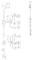
図5〜18は本発明の説明図である。
【0046】
図5は波長多重光信号の分波・受信方法を示している。第一と第二の反射面を、波長多重光信号の波長帯に対して透過性を示す材料で作製したプレート10の相対する2つの面に形成する。
【0047】
回折格子3は一方の反射面の一部に形成され、他方の反射面側には、波長多重信号光をプレートを通して回折格子に入射できる透過窓11が設けられている。
【0048】
波長多重信号光5は、回折格子3に対して角度φで入射し、波長毎に異なる角度θ1、θ2で回折光を生じる。回折によって波長毎に分離された信号光6は、第一の反射面と第二の反射面の間をそれぞれ異なる角度で反射伝搬し、信号光間の空間的な分離距離が広がる。適当な分離距離が得られた後、各信号光を取り出し窓12から取り出し、光電変換素子7で受信する。
【0049】
レンズ8は、回折光が光電変換素子7の受光面9で集光するように配置されている。
【0050】
ここで、回折格子3で生じる回折光は、下式を満足する回折角θで放射される。
【0051】
θ= sin-1(mNλ/n− sinφ)
φ:入射光の入射角
m:回折次数(m=0、±1、±2、・・・)
N:回折格子の溝本数(単位長さ当たりの溝本数)
λ:波長(真空中)
n:回折光が出射する媒質の屈折率
図5では、プレート10を第一の反射面1と第二の反射面2の距離が徐々に変化するような楔型としているが、平行平板でも良い。
【0052】
プレート材質は、ガラス、シリコン等を使用することが出来る。
【0053】
また、透過窓11と取り出し窓12は、波長多重信号の波長帯に対して無反射処理を施してあることが望ましい。
【0054】
また、回折格子は、入射する信号光の波長に対して、一次回折光(m=1)のみが生じるように設定することが望ましい。
【0055】
さらに、回折格子として、ブレーズドグレーティングを選択することもできる。
【0056】
また、第一及び第二の反射面は、金属膜や誘電体多層膜を使用することができる。反射率は100%に設定されることが望ましい。
【0057】
図6は、上記分波・受信方法の実装手段(PDパッケージ)を示している。
【0058】
電気リード端子22を有するステム21上に、光電変換素子7と回折格子プレート10を所定の位置に搭載する。プレートの楔角度とプレートが搭載される土台23は、回折格子への入射角φが所定の角度となるように予め設定されている。
【0059】
レンズ8は、ステムのキャップと一体に形成され、レンズキャップ24をステム21上の固定することにより、光電変換素子7の気密封止と同時に光学系を形成する。
【0060】
波長多重光信号の分波・受信方法は、図7の構成をとることもできる。
【0061】
プレートとして楔型形状を選択し、一方の反射面には回折格子3と反射膜31が形成されている。
【0062】
波長多重信号光5は、回折格子3に対して角度φで入射し、波長毎に異なる角度θ1、θ2で回折光を生じる。このとき、第一あるいは第二の反射面における回折光の反射は、少なくとも最初の1回目が、スネルの法則に従う全反射条件を満足するように回折角度θが設定される。
【0063】
回折によって波長毎に分離された信号光6は、第一の反射面と第二の反射面の間を反射伝搬し、全反射条件を満足しない反射点で外部に取り出され、光電変換素子7で受信される。レンズ8は、回折光が光電変換素子7の受光面9で集光するように配置されている。
【0064】
図7の分波・受信方法は、図8の如く光電変換素子7を回折格子プレート10上に搭載してPDパッケージを搭載することもできる。この際、回折格子プレート上に予め電極パターンを形成し(図示せず)、光電変換素子と電気接続しても良い。
【0065】
図9は、上記PDパッケージを用いたモジュールの構成手段を示している。
【0066】
波長多重光信号が含まれる近接波長帯(λ1、λ2、・・・)と、前記近接波長帯と離れた他の波長帯(λ0)を分離するプリズム形の波長合分波カプラ42を、光ファイバ44を内蔵したフェルール43端面に固定する。
【0067】
ここで、プリズムカプラ42の向きは、近接波長帯の光をファイバ光軸と垂直方向に反射させ、近接波長帯と離れた他の波長帯の光を光軸方向に透過させる向きに設定されている。
【0068】
光軸方向に、近接波長帯と離れた他の波長帯の光を発光するLD素子45を内蔵したLDパッケージ46を配置する。
【0069】
また、光軸と垂直方向に、前記多波長信号の受信が可能なPDパッケージ30(または20)を配置し、これら部材を単一のケース部材47で固定支持する。
【0070】
ここで、フェルール先端部近傍の外周面の一部を切削削除した切り欠きを設けても良い。
【0071】
LD45からの送信光λ0は、合分波カプラ42をそのまま光軸方向に通過(直進)して光ファイバ44に送信される。
【0072】
一方、光ファイバ44からの波長多重信号光(λ1、λ2、・・・)は、合分波カプラ42でファイバ光軸と垂直方向に反射され、PDパッケージ30(または20)に入射する。
【0073】
PDパッケージに入射した波長多重信号光は、回折格子プレート10で分離されPD素子7に受信される。
【0074】
これにより、図10の機能を有する波長多重双方向光伝送モジュールが実現できる。
【0075】
尚、図9において、LDパッケージとPDパッケージを入れ換えるように、合分波カプラを選択しても良い。
【0076】
図11は、さらに他の分波・受信構成を示している。
【0077】
光電変換素子7はプレート10上に搭載され、プレート内を反射伝搬する回折光6は光電変換素子7の基板を通して受光面9に導かれる。
【0078】
第一あるいは第二の反射面における回折光の反射が、スネルの法則に従う全反射条件を満足するように回折角度θを設定し、全反射膜無しの構成としている。
【0079】
光電変換素子7の屈折率をプレート10の屈折率よりも大きく設定することで、光電変換素子搭載部では全反射条件が崩れるため、回折光は光電変換素子側に取り出され受光部7に導かれる。
【0080】
図12は、図11の分波・受信方法の実装手段(LD/PDパッケージ)を示している。
【0081】
図12の如く、回折格子プレート10上に、近接波長帯と、近接波長帯と離れた他の波長帯を分離するプリズム型合分波カプラ42、近接波長帯の多重光信号を受信するPD素子7、および、近接波長帯と離れた他の波長光を発光するLD45を搭載したサブアセンブリを構成する。
【0082】
この際、回折格子プレート10上で、LD45からの迷光をPD7で受信(漏話)することを避けるために、PD素子をLD出射方向の延長上に配置しないことが望ましい。
【0083】
このサブアセンブリを電気リード端子22を有するステム21上の所定の位置に搭載する。
【0084】
ここで、図12のように、LD45はヒートシンク46−1を介して回折格子プレート10上に搭載されていても良く、同時にモニタPD47を搭載しても良い。
【0085】
また、回折格子プレート上に予め電極パターン48を形成し(図示せず)、前記LD45、PD7、モニタPD47と電気接続することもできる。
【0086】
回折格子プレート10は、LDの放熱を考慮すると熱伝導性の優れたシリコン等の半導体を使用することが望ましい。
【0087】
レンズ8は、ステムのキャップと一体に形成され、レンズキャップ24をステム上に固定することにより、光電変換素子7の気密封止と同時に光学系が形成できる。
【0088】
図13は、上記LD/PDパッケージ80を用いたモジュールの構成手段を示している。
【0089】
LD/PDパッケージ80にホルダ91を固定した後、フェルール付きファイバコード92を最適位置で調整・固定する。これにより、図10の機能を有する波長多重双方向光伝送モジュールが実現できる。
【0090】
さらに、図14〜16は波長多重伝送方法の他の実装手段(LD/PDパッケージ)を示している。
【0091】
図14の如く、回折格子プレート10上に、近接波長帯と、近接波長帯と離れた他の波長帯を分離するプリズム形合分波カプラ42、および、近接波長帯と離れた他の光を発光するLD45を搭載したサブアセンブリ50を構成する。
【0092】
このサブアセンブリ50と近接波長帯の多重光信号を受信する光電変換素子(PD素子)7を、図15、16のように、電気リード端子22を有するステム21上の所定の位置に搭載する。
【0093】
プレート10の楔角度とプレートが搭載される土台23は、回折格子3への入射角φが所定の角度となるように予め設定されている。
【0094】
この際、LD42からの迷光をPD素子7で受光(漏話)することを避けるために、回折格子プレート10の第一の反射面または第二の反射面にLD光をカットする膜61を形成することが望ましい。
【0095】
ここで、図14に記載のように、LD45はヒートシンク46−1を介して回折格子プレート10上に搭載されていても良く、同時にモニタPD47を搭載しても良い。
【0096】
また、回折格子プレート上に予め電極パターン48を形成し、前記LD、モニタPDと電気接続することもできる。
【0097】
回折格子プレート10は、LDの放熱を考慮すると熱伝導性の優れたシリコン等の半導体を使用することが望ましい。
【0098】
レンズ8は、ステムのキャップと一体に形成され、レンズキャップ24をステム上に固定することにより、光電変換素子7の気密封止と同時に光学系が形成できる。
【0099】
図17は、上記LD/PDパッケージ60を用いた他のモジュールの構成手段を示している。
【0100】
波長多重光信号が含まれる近接波長帯を第一の近接波長帯(λ1、λ2、・・)と第二の近接波長帯(λ11、λ12、・・・)に二分するプリズム形の波長合分波カプラ101を、光ファイバ44を内蔵したフェルール43端面に固定する。
【0101】
ここで、プリズムカプラ101の向きは、第一の近接波長帯の光をファイバ光軸方向に透過させ、第二の近接波長帯の光を光軸と垂直方向に反射させる向きに設定されている。
【0102】
さらに、プリズムカプラ101は、近接波長帯と離れた他の波長帯(λ0)の光をファイバ光軸方向に透過させる特性を同時に有するように設定される。
【0103】
光軸方向に図14〜16記載のLD/PDパッケージ60を配置し、光軸と垂直方向に図8、9記載のPDパッケージ30を配置し、これら部材を単一のケース部材47で固定支持する。
【0104】
光ファイバからの波長多重信号光(λ1、λ2、・・、λ1’、λ2’、・・)は、合分波カプラ101で分離され、第一の近接波長帯(λ1、λ2、・・・)はファイバ光軸方向に透過しLD/PDパッケージ60に入射する。また、第二の近接波長帯(λ1’、λ2’、・・・)はファイバ光軸と垂直方向に反射し、PDパッケージ30(または20)に入射する。
【0105】
LD/PDパッケージ60に入射した第一の近接波長帯の多重信号光は、第一の回折格子プレート10で分離され第一のPDアレイ素子7で受信される。
【0106】
PDパッケージ30に入射した第二の近接波長帯の多重信号光は、第二の回折格子プレート10’で分離され第二のPDアレイ素子7’で受信される。
【0107】
また、LD/PDパッケージ60に内蔵されたLD(図示せず、詳細は図16参照)からの送信光λ0は、合分波カプラ101をそのまま光軸方向に通過(直進)して光ファイバに送信される。
【0108】
これにより、図18の機能を有する波長多重双方向光伝送モジュールが実現できる。
【0109】
尚、図17において、LD/PDパッケージとPDパッケージを入れ換えるように、合分波カプラを選択しても良い。
【0110】
ここで、上記全てに共通して、近接波長帯の多重信号光を受信する光電変換素子は分離された各波長の信号に対応する独立した受光面を有するアレイ形状とすることもできる。
【0111】
本発明では、図5の如く、波長多重信号5を回折格子3で分波し、波長毎に異なる回折角で放射される各信号光6を2つの反射面間で複数回反射伝搬させることにより、コンパクトな構成で信号光間の空間分離距離を大きくとることができ、且つ、分離した信号光6を一方向から取り出すことが出来る。
【0112】
このため、従来例1のように、各信号光の分離方向が多方向に分散することが無く、モジュールをシンプルな構成で実現できるメリットがある。
【0113】
また、本発明の構成は、波長多重数に関係なく反射率100%の対向する反射膜とその一部に1種類の回折格子を必要とするだけである。
【0114】
従来例1のように、波長多重数以上に、特性の異なる誘電体多層膜を必要とする構成と比べて、低コスト化が図れる。
【0115】
回折格子プレートの材料として、ガラスを選択すれば平面度の高い2つの面を任意の楔角度で精度良く作製することが容易であり、且つ、生産性も高く低コスト化の効果が高い。
【0116】
さらに、回折格子プレート内の回折光を全反射条件で伝搬させれば、回折格子プレートの反射面に反射膜を形成する必要も無くなる。
【0117】
回折格子プレートを楔形とすれば、回折光の反射伝搬の周期を徐々に短くすることができ、平行平板のプレートと比べて長さを短くすることができる。
【0118】
また、プレート内を反射伝播する回折光が全反射(反射膜不要)条件となる角度で放射されても、プレートが楔形であれば、伝搬途中で全反射条件を満足しない条件を作ることができ、回折光をプレートの外(空気中)に取り出すことが可能となる。
【0119】
光電変換素子を回折格子プレート上に搭載し、また、同回折格子プレート上に光電変換素子への通電用電極パターンを作製すれば、従来必要とされた光電変換素子用のキャリアを不要とし、部品数の削減・集積小型化が実現できる。
【0120】
また、回折格子プレート上に搭載する光電変換素子あるいは接着材の屈折率を回折格子プレートの屈折率よりも大きい値に設定すれば、プレート内を伝搬する回折光が全反射条件で反射伝搬しても、光電光変換素子搭載部では全反射条件を満足しないため、回折光を光電変換素子へ導き出すことができる。
【0121】
上記、回折格子プレートは、1枚で複数の多重信号を分波可能である。
【0122】
対応する受信PDもアレイ形状とすればPD素子も小型化が可能となるため、分波・受信機能を小型パッケージに収納することができる。市販のLDまたはPDパッケージに用いられる電気リード端子付きステムとレンズキャップで気密パッケージすることもできる。
【0123】
これは、すなわち、従来のモジュール化技術で、本発明に基づく波長多重双方向光伝送モジュールを容易に実現できることを意味する。
【0124】
近接波長帯の波長多重信号と近接波長帯から離れた他の波長帯(λ0)を分離する合分波カプラと、回折格子プレートを収納した多波長受信PDパッケージ(図6、8)と、波長λ0の光電変換素子(LD)を内蔵したLDパッケージを組み合わせれば、従来の組立技術で容易に、図11に示す機能を実現することができる。
【0125】
同様に、回折格子プレートと受信PD素子、送信LD素子、および受信波長と送信波長を分離する合分波プリズムカプラを集積したLD/PDパッケージを用いれば、図10、18の機能を容易に実現することができる。
【0126】
また、上記LD/PDパッケージにおいて、送信LD素子と受信PD素子を回折格子プレートを挟んで互いに反対の位置に配置し、回折格子プレートに送信LDの発光波長の光をカットする膜を設ければ、送信LDから受信PDへの漏話を低減することができる。
【0127】
従って、上記作用により、波長多重双方向光伝送モジュールに関して、従来の不具合を解消し、且つ、より高機能なモジュールを従来の製造方法で容易に提供できる。
【0128】
また、小型、低コスト化が容易に実現できる。
【0129】
図5は本発明による波長多重光信号の分波・受信方法の例を示している。
【0130】
第一および第二の反射面として、ガラスで作製した楔形プレート10の相対する2面を選択した。
【0131】
第一の反射面1の一部分に、波長多重光5を分離するための回折格子3が形成してある。
【0132】
回折格子は、従来の干渉露光によるパターン形成技術と、RIE(リアクティブイオンエッチング)法による溝加工技術で容易に作製できる。
【0133】
その後、金属膜31を成膜する。このとき、取り出し窓12には金属膜を成膜しないことに注意する。第二の反射面2には、波長多重信号光がプレートを通して回折格子3に入射できる透過窓11を除き金属膜32が成膜してある。
【0134】
金属膜は、例えばチタン(Ti)、金(Au)の積層膜から成る。
【0135】
この構成にて、波長多重信号光5は透過窓11を通過して、ガラス媒質中で回折格子3に角度φで入射し波長毎に異なる角度θ1、θ2で回折光を生じる。
【0136】
ここで、例えば2波の多重光信号(λ=1490nm、1550nm)に対し、回折格子および楔形プレートに関するパラメータは下記の値に設定される。
【0137】
回折格子の溝本数N:800本/mm
波長多重光の入射角φ(ガラス媒質中):14°
波長1490nmの回折角θ1(ガラス媒質中):33.6°(m=1)
波長1550nmの回折角θ2(ガラス媒質中):35.8°(m=1)
楔形プレートの楔角度:14°
多重反射光の入射位置のプレート厚みt:2mm
上記条件にて、例えば図6の如く、第二の反射面間を1回反射し取り出し窓12から出射させると、波長1490nmの光信号と波長1550nmの光信号を約300μm離した空間分離が実現できる。
【0138】
空間分離された各信号光の位置に対応して光電変換素子(PD素子)7を配置すれば、多重信号光の分波・受信が可能となる。また、レンズ8は、PD素子の受光面9上で各信号光が集光するために用いる。これにより、隣接信号間の受信漏話を低減できる。
【0139】
ここで、楔形プレートの材料としてガラスを選択したが、シリコンやインジウムリン等、多重波長信号光に対し透過性を示す材料が適用できる。
【0140】
また、反射膜31、32は誘電体多層膜でも良く、このとき反射率は100%に設定されることが望ましい。
【0141】
また、透過窓11と取り出し窓12は、波長多重信号の波長帯に対して無反射処理を施してあることが望ましい。
【0142】
図6は、図5記載の構成を実装したPDパッケージの例である。電気リード端子22を有するステム21上に、光電変換素子7と楔形プレート10を所定の位置に搭載する。
【0143】
例えば、エポキシ接着材で接着固定される。
【0144】
ステムに形成された楔形プレート用の土台23は、回折格子3への入射角φが所定の角度となるよう予め設定されている。
【0145】
レンズ8はステムのキャップと一体に形成されており、このレンズキャップ24をステムにプロジェクション溶接して、光電変換素子の気密封止と同時に光学系を形成する。
【0146】
このときレンズの位置は、回折光が光電変換素子の受光面上で集光するように設計、調整される。
【0147】
図7は、波長多重光信号の分波・受信方法の第二の実施例を示している。
【0148】
第一および第二の反射面として、TaFガラス(屈折率1.8)で作製した楔型プレート10の相対する2面を選択した。
【0149】
第一の反射面1には、その一部に回折格子3を形成し、その上に金属膜31が成膜してある。
【0150】
第二の反射面には反射膜を成膜せず、少なくとも回折光の最初の反射が、スネルの法則に従う全反射条件を満足するように、例えば、2波の多重光信号(λ=1490nm、1550nm)に対し、各パラメータが下記の値に設定される。
【0151】
回折格子の溝本数:1000本/mm
波長多重光の入射角φ(ガラス媒質中):14°
波長1490nmの回折角θ1(ガラス媒質中):48.8°(m=1)
波長1550nmの回折角θ2(ガラス媒質中):52.4°(m=1)
楔形プレートの楔角度:14°
多重反射光の入射位置のプレート厚み:2mm
上記条件にて、回折格子で生じた回折光の第二反射面における最初の反射は、全反射条件となる。
【0152】
その後、プレートが楔形状のため、回折光は全反射条件が崩れ、第一の反射面の反射膜で反射した後、第二の反射面を通過して空間分離光が出射される。
【0153】
この時、波長1490nmの光信号と波長1550nmの光信号を約250μm離した空間分離が実現できる。
【0154】
空間分離された各信号光の位置に対応して、光電変換素子(PD素子)7を配置すれば、多重信号光の分波・受信が可能となる。
【0155】
また、レンズ8は、PD素子の受光面9上で各信号光が集光するために用いる。
【0156】
これにより、隣接信号間の受信漏話を低減できる。
【0157】
図8は、図7記載の構成を実装したPDパッケージの例である。
【0158】
図8の如く光電変換素子7を回折格子プレート10上に搭載することもできる。
【0159】
光電変換素子7は、例えば透明エポキシ接着材で固定する。
【0160】
この際、回折格子プレート上に予め電極パターンを形成し(図示せず)、光電変換素子と例えばAuワイヤで電気接続することもできる。
【0161】
図9は、図6または図8に記載のPDパッケージを用いた波長多重双方向光伝送モジュールの構成例を示している。
【0162】
このモジュールは、基本的には、波長多重信号を受信する前記PDパッケージ30(又は20)と、光送信部をなすLDパッケージと、波長合分波カプラ42を取り付けたフェルール付きファイバアセンブリとを単一のケース部材47で固定支持した構造を備える。
【0163】
合分波カプラ42は、受信信号である波長多重信号光(例えばλ1=1490nm、λ2=1550nm)と、これと離れた他の波長帯(送信信号;例えばλ0=1310nm)を合分波する膜を備えたプリズム形カプラであり、例えば1辺が1mmの立方形状からなる。
【0164】
この合分波カプラ42を、フェルール43の先端面光軸上に接着剤で直接固定する。
【0165】
ここで、合分波カプラの向きは、受信信号をファイバ光軸と垂直方向に反射させ、送信信号を光軸方向に透過させる向きに設定する。
【0166】
そして、LDパッケージ46を光軸方向に、PDパッケージ30(または20)を光軸と垂直方向に配置し、最適位置となるように光軸調整後、例えばレーザ溶接で固定する。
【0167】
LD45からの送信光(λ0=1310nm)は、合分波カプラ42をそのまま光軸方向に通過(直進)して光ファイバ44に送信される。
【0168】
一方、光ファイバ44からの波長多重信号光(λ1=1490nm、λ2=1550nm)は、合分波カプラ42でファイバ光軸と垂直方向に反射され、PDパッケージ30(または20)に入射する。
【0169】
PDパッケージに入射した波長多重信号光は、回折格子プレート10で分離されPD素子7に受信される。
【0170】
これにより、図10の機能を有する波長多重双方向光伝送モジュールが実現できる。
【0171】
図11は、波長多重光信号の分波・受信方法の第三の実施例を示している。
【0172】
第一および第二の反射面として、ガラスで作製した平行平板プレート10の相対する2面を選択した。
【0173】
第一の反射面1には、その一部に回折格子3を形成し、その上に金属膜31が成膜してある。
【0174】
回折格子のパラメータは、第一および第二の反射面における回折光の反射がスネルの法則に従う全反射条件を満足するように設定され、例えば、2波の多重光信号(λ=1490nm、1550nm)に対し下記値となる。
【0175】
回折格子の溝本数N:1000本/mm
波長多重光の入射角φ(空気中):28°
〃 (ガラス媒質中):18°
波長1490nmの回折角θ1(ガラス媒質中):42.9°(m=1)
波長1550nmの回折角θ2(ガラス媒質中):46.1°(m=1)
平行平板プレートの厚みt:1.5mm
上記条件にて、回折光は全反射条件でプレート内を伝搬するので、回折格子部分以外に全反射膜を形成する必要はない。
【0176】
光電変換素子(PD素子)7は、平行平板プレート10上に例えば光学的に透明な接着材(図示せず)で固定される。
【0177】
ここで、PD素子7および接着剤は、平行平板プレートを構成するガラスの屈折率よりも大きい値の材料を選択する。
【0178】
例えばガラス(屈折率1.5)に対して、PD素子をインジウムリン(屈折率3.4)、接着剤を透明エポキシ(屈折率1.65)とすれば良い。これにより、PD素子搭載部では全反射条件が崩れるため、回折光はPD素子側に取り出され受光部に導かれる。
【0179】
図12は、図11を用いた波長多重双方向伝送方法の他の実装例(LD/PDパッケージ)を示している。
【0180】
図12の如く、図11と同等の並行平板の回折格子プレート10の上に、受信信号である波長多重信号光(例えばλ1=1490nm、λ2=1550nm)と、これと離れた他の波長帯(送信信号;例えばλ0=1310nm)を合分波するプリズム形カプラ42、
受信用PD素子7、送信用LD素子45(例えばλ0=1310nm)、およびモニタPD素子45を搭載する。
【0181】
合分波カプラ42の向きは、LDからの送信光が上方へ光路変換されるように設定される。
【0182】
また、LD素子45、モニタPD素子47はそれぞれヒートシンク46−1、サブキャリア49を介して回折格子プレート上に配置し、各光素子(LD45、PD7、モニタPD47)は回折格子上の電極パターン(図示せず)と例えばAuワイヤで電気接続される。
【0183】
光素子を搭載した回折格子プレートは、電気リード22を有するステム21上の所定の位置に搭載される。
【0184】
レンズ8はステムのキャップと一体に形成されており、このレンズキャップ24をステムにプロジェクション溶接して、光電変換素子の気密封止と同時に光学系を形成する。
【0185】
このときレンズの位置は、少なくとも回折格子プレート10内で生じる回折光が光電変換素子7の受光面上で集光するように設計、調整される。この構成により、LD45から出射した光(例えばλ=1310nm)は、合分波カプラ42で反射して上方に光路変換し、レンズ8により集光された光を出射する。
【0186】
また、レンズ8を通して入射した波長多重信号(例えばλ1=1490nm、λ2=1550nm)は、回折格子プレートで分波され、PD素子7で受光される。
【0187】
図13は、上記LD/PDパッケージを用いた波長多重双方向光伝送モジュールの構成例を示している。LD/PDパッケージにホルダ91をプロジェクション溶接で固定後、フェルール付きファイバコード92をスリーブ93を通してホルダ91上に配置する。
【0188】
フェルール94の位置を調整し、LD45からの出力光(例えばλ0=1310nm)と波長多重信号(例えばλ1=1490nm、λ2=1550nm)に対するPD7の受光感度が共に最大となる最適位置で、ホルダ91とフェルール94をスリーブ93を介してレーザ溶接で固定する。
【0189】
これにより、図9のモジュールと同じ機能(図10)をさらに小型のモジュールで実現することができる。
【0190】
さらに、図14〜16は波長多重双方向伝送方法の他の実装例(LD/PDパッケージ)を示している。
【0191】
図14の如く、図5と同等の楔形回折格子プレート10の上に、受信信号である波長多重信号光(例えばλ1=1490nm、λ2=1550nm)と、これと離れた他の波長帯(送信信号;例えばλ0=1310nm)を合分波するプリズム形カプラ42、および、送信用LD素子(例えばλ0=1310nm)45、モニタPD素子47を搭載する。
【0192】
合分波カプラ42の向きは、LDからの送信光が上方へ光路変換されるように設定される。
【0193】
また、LD素子45、モニタPD素子47は、それぞれヒートシンク46−1、サブキャリア49を介して回折格子プレート10上の電極パターン48と例えばAuワイヤで電気接続される。
【0194】
この回折格子プレートと光電変換素子を、図6と同様に、電気リード端子22を有するステム21上の所定の位置に搭載する。
【0195】
ステムに形成された楔形プレート用の土台23は、回折格子への入射角φが所定の角度となるよう予め設定されている。
【0196】
レンズ8はステムのキャップと一体に形成されており、このレンズキャップ24をステムにプロジェクション溶接して、光電変換素子の気密封止と同時に光学系を形成する。このときレンズの位置は、少なくとも回折格子プレート10内で生じる回折光が光電変換素子7の受光面上で集光するように設計、調整される。
【0197】
図15は、完成したLD/PDパッケージを図14A方向から見た断面図を示す。これは、図8と同じ構成であり、レンズ8を通して入射した波長多重信号(例えばλ1=1490nm、λ2=1550nm)の受信が実現できる。
【0198】
図16は、完成したLD/PDパッケージを図14B方向から見た断面図を示す。これは、送信部を説明する図になっている。
【0199】
LD45から出射した光(例えばλ=1310nm)は、合分波カプラ42で反射して上方に光路変換し、レンズ8により集光された光を出力する。
【0200】
ここで、回折格子プレート上に搭載されたLD45からの迷光をPD素子7で受光(漏話)することを避けるために、図15の如く、回折格子プレート10の第一反射面側にLWPF(Long Wavelength Pass Filter )61を設けた。
【0201】
回折格子プレート10は、LDの放熱性を考慮すると熱伝送性の優れたシリコン等の半導体を使用しても良い。
【0202】
図17は、図14〜16のLD/PDパッケージを用いたモジュールの実施例を示している。
【0203】
このモジュールは、基本的には、波長多重信号を受信する前記PDパッケージ30(または20)と、LD/PDパッケージ60(または80)と、波長合分波カプラ101を取り付けたフェルール付きファイバアセンブリとを単一のケース部材47で固定支持した構造を備える。
【0204】
フェルール43の先端に取り付けられる合分波カプラ101は、受信信号である波長多重信号光を第一の近接波長帯(例えばλ1=1485nm、λ2=1505nm)と第二の近接波長帯(例えばλ1’=1545nm、λ2’=1555nm)に2分する膜を備えたプリズム形カプラであり、例えば1辺が1mmの立方形状からなる。
【0205】
この合分波カプラ101を、フェルール43の先端面光軸上に接着剤で直接固定する。
【0206】
ここで、合分波カプラの向きは、第二の近接波長帯の光をファイバ光軸と垂直方向に反射させ、第一の近接波長帯の光を光軸方向に透過させる向きに設定する。
【0207】
また、LD/PDパッケージ60(または80)に内蔵されたLD(図示せず。図16参照のこと。)の出射光(例えばλ0=1310nm)も第一の近接波長帯と同じく光軸方向に透過する。
【0208】
そして、LD/PDパッケージ60(または80)を光軸方向に、PDパッケージ30(または20)を光軸と垂直方向に配置し、最適位置となるように光軸調整後、例えばレーザ溶接で固定する。
【0209】
LDからの送信光(λ0=1310nm)は、合分波カプラ101をそのまま光軸方向に通過(直進)して光ファイバ44に送信される。(図17中、LD/PDパッケージはLDが見えない方向から見た断面図となっていることに注意。図16参照。)
一方、光ファイバ44からの波長多重信号光のうち、第二の近接波長帯の多重光信号(λ1=1485nm、λ2=1505nm)は、合分波カプラ101でファイバ光軸と垂直方向に反射され、PDパッケージ30(または20)に入射する。
【0210】
PDパッケージに入射した波長多重信号光は、回折格子プレート10’で分離されPD素子7’に受信される。
【0211】
また、第一の近接波長帯の多重光信号(λ1’=1545nm、λ2’=1555nm)は、合分波カプラ101を通過し、LD/PDパッケージ60(または80)に入射する。
【0212】
LD/PDパッケージに入射した波長多重信号光は、合分波カプラ42を通過し回折格子プレート10で分離されPD素子7に受信される。
【0213】
これにより、図18の機能を有する波長多重双方向光伝送モジュールが実現できる。
【0214】
ここで、上記全ての実施例に共通して、光電変換素子は分離された各波長の信号に対応する独立した受光面を有するアレイ形状とすることもできる。
【0215】
また、回折効率の観点から、上記3つの実施例はいずれも一次回折光のみが存在する条件に設定したが、さらに高効率化を図るために回折格子の形状をブレーズドグレーティングとすることもできる。
【0216】
【発明の効果】
以上説明したように、本発明によれば波長多重双方向光伝送に適用される光モジュールに関し、従来の製造方法で容易に作製できるハイブリッド集積型モジュール構成において高機能化を実現できる手段を提供し、係る光モジュールの高機能化、小型、低価格化に寄与するところが大きい。
【図面の簡単な説明】
【図1】従来の通信方式
【図2】本発明が適用可能な通信方式
【図3】従来例(1)
【図4】従来例(2)
【図5】波長多重光の分波、受信方法を示す図(1)
【図6】PDパッケージ(1)
【図7】波長多重光の分波、受信方法を示す図(2)
【図8】PDパッケージ(2)
【図9】波長多重双方向光伝送モジュール(1)
【図10】波長多重双方向光伝送モジュールの機能(1)
【図11】波長多重光の分波・受信方法を示す図(3)
【図12】LD/PDパッケージ(1)
【図13】波長多重双方向光伝送モジュール(2)
【図14】サブアセンブリ(1)
【図15】LD/PDパッケージ(2)
【図16】LD/PDパッケージ(3)
【図17】波長多重双方向光伝送モジュール(3)
【図18】波長多重双方向光伝送モジュールの機能(2)
【符号の説明】
3 回折格子
5 波長多重信号光
6 信号光
7 光電変換素子
8 レンズ
9 受光面
10 プレート
11 透過窓
12 取り出し窓
21 ステム
22 電気リード端子
23 土台
24 レンズキャップ
30 PDパッケージ
42 波長合分波カプラ
43 フェルール
44 光ファイバ
45 LD素子
46 LDパッケージ
46−1 ヒートシンク
50 サブアセンブリ
60 LD/PDパッケージ
61 膜
80 LD/PDパッケージ
91 ホルダ[0001]
[Industrial application fields]
The present invention relates to an optical module applied to the field of optical communication, and more particularly, to an optical coupling form for realizing bidirectional optical transmission of wavelength multiplexed signals and a mounting method thereof.
[0002]
In order to cope with the rapid increase in network traffic accompanying the rapid growth of the Internet, the development of communication networks using wavelength division multiplexing is progressing mainly in the trunk line system.
[0003]
In a wavelength division multiplexing (WDM) communication system, a plurality of optical signals (channels) having different wavelengths are simultaneously transmitted through one optical fiber. For this reason, the optical transmission module is required to have a multiplexing / demultiplexing function (WDM function) and bidirectional transmission (transmission / reception function) for distributing optical signals of different wavelengths.
[0004]
Wavelength multiplexing of optical communication extends not only to basic communication systems but also to subscriber optical communication systems drawn to offices and homes. At present, optical subscriber communication is put into practical use by the method (example) shown in FIG. This is an uplink transmission in the 1.3 μm band (1260 to 1360 nm) and a downlink transmission in the 1.55 μm band (1480 to 1580 nm), which is called an ATM-PON system. This is a transmission of one channel each for uplink and downlink.
[0005]
However, as described at the beginning, with the rapid growth of the Internet, there is a strong demand for realizing higher-speed and broadband services in optical subscriber communications.
[0006]
For this reason, a method shown in FIG. 2 in which the number of wavelength multiplexing is further increased has been studied.
[0007]
The downstream 1.55 μm band is divided to increase the service provided.
[0008]
On the other hand, the greatest demand for optical modules (optical devices) applied to these optical subscriber systems is low cost and miniaturization.
[0009]
In order to realize the module applicable to the system of FIG. 2, in addition to the LD for transmission and the PD for reception, the 1.3 μm and 1.55 μm coupling / demultiplexing couplers, the WDM function that further separates the 1.55 μm band Therefore, how to realize these functions at a small size and at a low cost is a key point for system diffusion.
[0010]
Against this backdrop, optical transmission modules are being developed to achieve mass production and lower costs by hybrid integration of WDM couplers and light transmitting / receiving elements to reduce size, reduce the number of parts, and simplify the assembly process. It is out.
[0011]
In response to such a need, the present invention intends to provide a configuration of a low-cost, small-sized wavelength division multiplexing optical transmission module that can be applied to the next generation optical subscriber communication system as shown in FIG. .
[0012]
[Prior art]
For example, the following techniques are known as conventional examples of wavelength division multiplexing bidirectional optical transmission modules.
[0013]
FIG. 3 shows a module configuration described in Japanese Laid-Open Publication No. 61-226713 “Optical Module for Optical Wavelength Division Multiplexing” (Conventional Example 1).
[0014]
Transmission
[0015]
Then, a semiconductor light receiving element with a lens 223-1 (for receiving an optical signal having a wavelength λ3) 224 is provided on an extension of the central axis of the rod lens, and a semiconductor light emitting with a lens 223-3 is provided on the radial side of the rod lens. An element (for light signal emission of wavelength λ2) 225 and a semiconductor light-emitting element (for light signal emission of wavelength λ1) 226 with a lens 223-2 are arranged.
[0016]
The interference film filter includes a short wavelength pass filter and a long wavelength pass filter.
[0017]
With this configuration, the optical signal having the wavelength λ3 propagating through the transmission optical fiber passes through the
[0018]
Light from the semiconductor
[0019]
The
[0020]
Similarly, the light from the semiconductor
[0021]
This realizes three-wave multiplex bidirectional transmission.
[0022]
Further, Patent Publication 2000-180671 “Structure of optical transceiver module and manufacturing method thereof” (conventional example 2) shows a more specific configuration of the hybrid integrated module (see FIG. 4).
[0023]
A prism-shaped wavelength multiplexing /
[0024]
An LD package having a
[0025]
With this configuration, two-wave bidirectional transmission is realized. If Conventional Example 1 is applied, three-wave multiplex bidirectional transmission is also possible with the same technique.
[0026]
[Problems to be solved by the invention]
The problem with optical transmission devices is cost reduction and size reduction. Of these devices, the majority of the cost is related to an optical module having an optical multiplexing / demultiplexing / photoelectric conversion function.
[0027]
For this reason, along with the enhancement of functionality of optical modules, miniaturization, simplification of assembly processes, and cost reduction are important factors that cannot be ignored.
[0028]
However, the above-described conventional techniques have the following problems in realizing these.
[0029]
The interference film filter used in the conventional examples 1 and 2 is formed of a dielectric multilayer film such as SiO2 and TiO2, for example, and realizes a steep wavelength characteristic that separates adjacent wavelengths with a high extinction ratio. For this, the number of dielectric films must be increased and the film thicknesses must be accurately controlled.
[0030]
For this reason, a film that separates adjacent wavelengths is not feasible but very expensive.
[0031]
The configurations of the conventional examples 1 and 2 that require interference film filters of the number of wavelengths to be multiplexed or demultiplexed are difficult to realize low cost for multiplexing and demultiplexing of wavelength multiplexed signals. .
[0032]
Further, as is clear from Conventional Example 1, the multiplexing / demultiplexing of a plurality of wavelengths is achieved by dispersing the optical path in multiple directions.
[0033]
Along with this, the direction of the interference film filter also needs to be directed in multiple directions, and it is necessary to manufacture and assemble several kinds of irregular glass blocks and various interference film filters, which hinders mass productivity. It was.
[0034]
Furthermore, since the direction of optical path dispersion of wavelength multiplexing / demultiplexing is finite, the number of wavelengths that can be demultiplexed is limited.
[0035]
Further, the multiplexing / demultiplexing method in one wavelength / one direction requires the number of wavelength multiplexing (multiplexing / demultiplexing) LD or PD packages as described in the conventional example 2.
[0036]
For this reason, the number of wavelengths that can be demultiplexed is also limited by the arrangement of the LD or PD package.
[0037]
Furthermore, since the lead terminals of the LD / PD package are oriented in multiple directions, it is a serious problem that is not suitable for practical use. Of course, it is difficult to reduce the size of the module.
[0038]
The present invention has been made in view of the above-described problems of the prior art, and an object thereof is to provide a bidirectional optical transmission module capable of wavelength multiplexing at a small size and at low cost.
[0039]
[Means for solving problems]
As a first means,
The wavelength division multiplexing bidirectional optical transmission module has a diffraction grating formed on a part of one of the first and second reflecting surfaces of a translucent plate having first and second reflecting surfaces facing each other. And
Wavelength multiplexed signal light including light in at least two adjacent wavelength bands is incident on the diffraction grating,
Diffracted light generated at different angles for each wavelength of light is reflected and propagated between the first and second reflecting surfaces, and then received by individual photoelectric conversion elements for each separated signal light.
[0040]
As a second means,
In the wavelength division multiplexing bidirectional optical transmission module of the first means, the plate is a wedge-shaped plate in which the distance between the first and second reflecting surfaces facing each other gradually changes.
[0041]
As a third means,
In the wavelength division multiplexing bi-directional optical transmission module of the first and second means, the diffracted light is totally reflected according to Snell's law on a part of at least one of the opposing first and second reflecting surfaces. The diffraction angle of the diffracted light is set so as to reflect and propagate under conditions.
[0042]
As a fourth means,
In the wavelength division multiplexing bi-directional optical transmission module of the third means, a light transmissive material having a refractive index larger than the light refractive index of the material constituting the plate is used as the first to the first conditions where the diffracted light becomes a total reflection condition. The diffracted light that is brought into contact with a part of the two reflecting surfaces and reflected and propagates between the first and second reflecting surfaces is extracted to the outside.
[0043]
As a fifth means,
In the wavelength division multiplexing bidirectional optical transmission module of the first to fourth means, the diffraction grating plate having the first and second reflecting surfaces includes an optical filter film that reflects light in a specific wavelength band.
[0044]
DETAILED DESCRIPTION OF THE INVENTION
Embodiments of the present invention will be described below with reference to the drawings.
[0045]
5 to 18 are explanatory diagrams of the present invention.
[0046]
FIG. 5 shows a method of demultiplexing / receiving wavelength multiplexed optical signals. The first and second reflecting surfaces are formed on two opposing surfaces of the
[0047]
The
[0048]
The wavelength multiplexed
[0049]
The
[0050]
Here, the diffracted light generated by the
[0051]
θ = sin-1 (mNλ / n-sinφ)
φ: Incident light incident angle
m: Diffraction order (m = 0, ± 1, ± 2, ...)
N: Number of grooves in the diffraction grating (number of grooves per unit length)
λ: Wavelength (in vacuum)
n: Refractive index of the medium from which the diffracted light is emitted
In FIG. 5, the
[0052]
As the plate material, glass, silicon or the like can be used.
[0053]
Further, it is desirable that the transmission window 11 and the
[0054]
The diffraction grating is preferably set so that only the first-order diffracted light (m = 1) is generated with respect to the wavelength of the incident signal light.
[0055]
Further, a blazed grating can be selected as the diffraction grating.
[0056]
Moreover, a metal film and a dielectric multilayer film can be used for the first and second reflecting surfaces. The reflectivity is desirably set to 100%.
[0057]
FIG. 6 shows a mounting means (PD package) for the demultiplexing / receiving method.
[0058]
The
[0059]
The
[0060]
The wavelength division multiplexed optical signal demultiplexing / receiving method can take the configuration shown in FIG.
[0061]
A wedge shape is selected as the plate, and the
[0062]
The wavelength multiplexed
[0063]
The
[0064]
In the demultiplexing / receiving method of FIG. 7, the
[0065]
FIG. 9 shows module constituting means using the PD package.
[0066]
A prism-type wavelength multiplexing /
[0067]
Here, the direction of the
[0068]
In the optical axis direction, an
[0069]
A PD package 30 (or 20) capable of receiving the multi-wavelength signal is disposed in a direction perpendicular to the optical axis, and these members are fixedly supported by a
[0070]
Here, you may provide the notch which cut and deleted a part of outer peripheral surface of the ferrule front-end | tip part vicinity.
[0071]
The transmission light λ0 from the
[0072]
On the other hand, the wavelength multiplexed signal light (λ1, λ2,...) From the
[0073]
The wavelength multiplexed signal light incident on the PD package is separated by the
[0074]
Thereby, a wavelength division multiplexing bidirectional optical transmission module having the function of FIG. 10 can be realized.
[0075]
In FIG. 9, a multiplexing / demultiplexing coupler may be selected so that the LD package and the PD package are interchanged.
[0076]
FIG. 11 shows still another demultiplexing / receiving configuration.
[0077]
The
[0078]
The diffraction angle θ is set so that the reflection of the diffracted light on the first or second reflecting surface satisfies the total reflection condition according to Snell's law, and the total reflection film is not provided.
[0079]
By setting the refractive index of the
[0080]
FIG. 12 shows mounting means (LD / PD package) for the demultiplexing / receiving method of FIG.
[0081]
As shown in FIG. 12, on the
[0082]
At this time, in order to avoid receiving stray light from the
[0083]
This subassembly is mounted at a predetermined position on the
[0084]
Here, as shown in FIG. 12, the
[0085]
An electrode pattern 48 (not shown) may be formed in advance on the diffraction grating plate and electrically connected to the
[0086]
The
[0087]
The
[0088]
FIG. 13 shows module constituting means using the LD /
[0089]
After fixing the holder 91 to the LD /
[0090]
Further, FIGS. 14 to 16 show other mounting means (LD / PD package) of the wavelength multiplexing transmission method.
[0091]
As shown in FIG. 14, on the
[0092]
The sub-assembly 50 and a photoelectric conversion element (PD element) 7 that receives multiplexed optical signals in the near wavelength band are mounted at predetermined positions on the
[0093]
The wedge angle of the
[0094]
At this time, in order to prevent the stray light from the
[0095]
Here, as shown in FIG. 14, the
[0096]
Further, an
[0097]
The
[0098]
The
[0099]
FIG. 17 shows another module configuration means using the LD /
[0100]
Prism-shaped wavelength division that divides the adjacent wavelength band including the wavelength multiplexed optical signal into the first adjacent wavelength band (λ1, λ2,...) And the second adjacent wavelength band (λ11, λ12,...). The
[0101]
Here, the direction of the
[0102]
Further, the
[0103]
14-16 is arranged in the optical axis direction, and the
[0104]
Wavelength multiplexed signal light (λ1, λ2,..., Λ1 ′, λ2 ′,...) From the optical fiber is separated by the multiplexing /
[0105]
The multiplexed signal light in the first near wavelength band incident on the LD /
[0106]
The multiplexed signal light in the second near wavelength band incident on the
[0107]
Also, the transmission light λ0 from the LD (not shown, see FIG. 16 for details) built in the LD /
[0108]
Thereby, a wavelength division multiplexing bidirectional optical transmission module having the function of FIG. 18 can be realized.
[0109]
In FIG. 17, a multiplexing / demultiplexing coupler may be selected so that the LD / PD package and the PD package are interchanged.
[0110]
Here, in common with all of the above, the photoelectric conversion element that receives the multiplexed signal light in the near wavelength band may have an array shape having an independent light receiving surface corresponding to the separated signal of each wavelength.
[0111]
In the present invention, as shown in FIG. 5, the wavelength multiplexed
[0112]
For this reason, unlike the conventional example 1, the separation directions of the signal lights are not dispersed in multiple directions, and there is an advantage that the module can be realized with a simple configuration.
[0113]
Further, the configuration of the present invention only requires one type of diffraction grating for the opposing reflection film having a reflectance of 100% and a part thereof regardless of the number of wavelength multiplexing.
[0114]
The cost can be reduced as compared with the configuration requiring a dielectric multilayer film having different characteristics more than the number of multiplexed wavelengths as in Conventional Example 1.
[0115]
If glass is selected as the material of the diffraction grating plate, it is easy to accurately produce two surfaces with high flatness at an arbitrary wedge angle, and the productivity is high and the cost reduction effect is high.
[0116]
Furthermore, if the diffracted light in the diffraction grating plate is propagated under total reflection conditions, it is not necessary to form a reflection film on the reflection surface of the diffraction grating plate.
[0117]
If the diffraction grating plate is wedge-shaped, the period of reflection propagation of diffracted light can be gradually shortened, and the length can be shortened compared to a parallel plate.
[0118]
Even if diffracted light reflected and propagated in the plate is emitted at an angle that satisfies the condition of total reflection (no reflection film required), if the plate is wedge-shaped, conditions that do not satisfy the total reflection condition during propagation can be created. The diffracted light can be taken out of the plate (in the air).
[0119]
If the photoelectric conversion element is mounted on the diffraction grating plate and the electrode pattern for energizing the photoelectric conversion element is formed on the diffraction grating plate, the carrier for the photoelectric conversion element that has been required in the past is unnecessary, and the parts Number reduction and integration miniaturization can be realized.
[0120]
If the refractive index of the photoelectric conversion element or adhesive mounted on the diffraction grating plate is set to a value larger than the refractive index of the diffraction grating plate, the diffracted light propagating in the plate will be reflected and propagated under total reflection conditions. However, since the photoelectric conversion element mounting portion does not satisfy the total reflection condition, diffracted light can be led to the photoelectric conversion element.
[0121]
A single diffraction grating plate can demultiplex a plurality of multiplexed signals.
[0122]
If the corresponding receiving PD has an array shape, the PD element can be reduced in size, so that the demultiplexing / receiving function can be accommodated in a small package. It is also possible to perform airtight packaging with a stem with an electric lead terminal and a lens cap used for a commercially available LD or PD package.
[0123]
This means that the wavelength division multiplexing bidirectional optical transmission module according to the present invention can be easily realized by the conventional modularization technique.
[0124]
A multi-wavelength receiving PD package (FIGS. 6 and 8) containing a diffraction grating plate, a multiplexing / demultiplexing coupler that separates a wavelength division multiplexed signal in the near wavelength band and another wavelength band (λ0) far from the near wavelength band, and a wavelength If an LD package incorporating a photoelectric conversion element (LD) of λ0 is combined, the function shown in FIG. 11 can be easily realized by a conventional assembly technique.
[0125]
Similarly, the functions shown in FIGS. 10 and 18 can be easily realized by using an LD / PD package in which a diffraction grating plate, a reception PD element, a transmission LD element, and a multiplexing / demultiplexing prism coupler for separating a reception wavelength and a transmission wavelength are integrated. can do.
[0126]
Further, in the LD / PD package, if the transmission LD element and the reception PD element are arranged at positions opposite to each other with the diffraction grating plate interposed therebetween, a film that cuts light of the emission wavelength of the transmission LD is provided on the diffraction grating plate. The crosstalk from the transmission LD to the reception PD can be reduced.
[0127]
Therefore, with the above-described operation, the conventional problems relating to the wavelength division multiplexing bidirectional optical transmission module can be solved, and a more functional module can be easily provided by the conventional manufacturing method.
[0128]
In addition, the size and cost can be easily reduced.
[0129]
FIG. 5 shows an example of a wavelength division multiplexing optical signal demultiplexing / receiving method according to the present invention.
[0130]
Two opposing surfaces of the wedge-shaped
[0131]
A
[0132]
The diffraction grating can be easily manufactured by a conventional pattern formation technique by interference exposure and a groove processing technique by RIE (reactive ion etching).
[0133]
Thereafter, a
[0134]
The metal film is made of, for example, a laminated film of titanium (Ti) and gold (Au).
[0135]
With this configuration, the wavelength multiplexed
[0136]
Here, for example, for two-wave multiplexed optical signals (λ = 1490 nm, 1550 nm), the parameters relating to the diffraction grating and the wedge-shaped plate are set to the following values.
[0137]
Number of grooves of diffraction grating N: 800 / mm
Angle of incidence of wavelength multiplexed light φ (in glass medium): 14 °
Diffraction angle θ1 at a wavelength of 1490 nm (in a glass medium): 33.6 ° (m = 1)
Diffraction angle θ2 at a wavelength of 1550 nm (in a glass medium): 35.8 ° (m = 1)
Wedge angle of wedge plate: 14 °
Plate thickness t at the incident position of multiple reflected light t: 2 mm
Under the above conditions, for example, as shown in FIG. 6, when the second reflecting surface is reflected once and emitted from the
[0138]
If a photoelectric conversion element (PD element) 7 is arranged corresponding to the position of each signal light that has been spatially separated, it is possible to demultiplex and receive multiplexed signal light. The
[0139]
Here, glass is selected as the material of the wedge-shaped plate, but a material that is transparent to multi-wavelength signal light, such as silicon or indium phosphide, can be applied.
[0140]
Further, the
[0141]
Further, it is desirable that the transmission window 11 and the
[0142]
FIG. 6 is an example of a PD package in which the configuration shown in FIG. 5 is mounted. On the
[0143]
For example, it is bonded and fixed with an epoxy adhesive.
[0144]
The wedge-shaped
[0145]
The
[0146]
At this time, the position of the lens is designed and adjusted so that the diffracted light is condensed on the light receiving surface of the photoelectric conversion element.
[0147]
FIG. 7 shows a second embodiment of the demultiplexing / receiving method for wavelength multiplexed optical signals.
[0148]
Two opposing surfaces of the wedge-shaped
[0149]
A
[0150]
No reflection film is formed on the second reflection surface, and at least the first reflection of the diffracted light satisfies, for example, a total reflection condition according to Snell's law, for example, a two-wave multiplexed optical signal (λ = 1490 nm, 1550 nm), each parameter is set to the following value.
[0151]
Number of grooves of diffraction grating: 1000 / mm
Angle of incidence of wavelength multiplexed light φ (in glass medium): 14 °
Diffraction angle θ1 at a wavelength of 1490 nm (in a glass medium): 48.8 ° (m = 1)
Diffraction angle θ2 at a wavelength of 1550 nm (in a glass medium): 52.4 ° (m = 1)
Wedge angle of wedge plate: 14 °
Plate thickness at incident position of multiple reflected light: 2 mm
Under the above conditions, the first reflection of the diffracted light generated by the diffraction grating on the second reflecting surface is a total reflection condition.
[0152]
Thereafter, since the plate has a wedge shape, the total reflection condition of the diffracted light is lost, and after being reflected by the reflective film on the first reflective surface, the separated light is emitted through the second reflective surface.
[0153]
At this time, spatial separation can be realized by separating an optical signal having a wavelength of 1490 nm and an optical signal having a wavelength of 1550 nm by about 250 μm.
[0154]
If a photoelectric conversion element (PD element) 7 is arranged corresponding to the position of each signal light that has been spatially separated, it is possible to demultiplex and receive multiplexed signal light.
[0155]
The
[0156]
Thereby, reception crosstalk between adjacent signals can be reduced.
[0157]
FIG. 8 shows an example of a PD package in which the configuration shown in FIG. 7 is mounted.
[0158]
The
[0159]
The
[0160]
At this time, an electrode pattern (not shown) may be formed in advance on the diffraction grating plate and electrically connected to the photoelectric conversion element by, for example, an Au wire.
[0161]
FIG. 9 shows a configuration example of a wavelength multiplexing bidirectional optical transmission module using the PD package shown in FIG. 6 or FIG.
[0162]
This module basically includes a PD package 30 (or 20) that receives a wavelength multiplexed signal, an LD package that forms an optical transmitter, and a fiber assembly with a ferrule to which a wavelength multiplexing /
[0163]
The multiplexing /
[0164]
The multiplexing /
[0165]
Here, the direction of the multiplexing / demultiplexing coupler is set such that the reception signal is reflected in the direction perpendicular to the fiber optical axis and the transmission signal is transmitted in the optical axis direction.
[0166]
Then, the
[0167]
Transmitted light (λ0 = 1310 nm) from the
[0168]
On the other hand, the wavelength multiplexed signal light (λ1 = 1490 nm, λ2 = 1550 nm) from the
[0169]
The wavelength multiplexed signal light incident on the PD package is separated by the
[0170]
Thereby, a wavelength division multiplexing bidirectional optical transmission module having the function of FIG. 10 can be realized.
[0171]
FIG. 11 shows a third embodiment of the wavelength division multiplexing optical signal demultiplexing / receiving method.
[0172]
Two opposing surfaces of the
[0173]
A
[0174]
The parameters of the diffraction grating are set so that the reflection of the diffracted light on the first and second reflecting surfaces satisfies the total reflection condition according to Snell's law. For example, two-wave multiplexed optical signals (λ = 1490 nm, 1550 nm) Is the following value.
[0175]
Number of grooves of diffraction grating N: 1000 / mm
Wavelength multiplexed light incident angle φ (in air): 28 °
〃 (in glass medium): 18 °
Diffraction angle θ1 at a wavelength of 1490 nm (in a glass medium): 42.9 ° (m = 1)
Diffraction angle θ2 at a wavelength of 1550 nm (in a glass medium): 46.1 ° (m = 1)
Parallel plate thickness t: 1.5mm
Under the above conditions, the diffracted light propagates in the plate under the total reflection condition, so that it is not necessary to form a total reflection film other than the diffraction grating portion.
[0176]
The photoelectric conversion element (PD element) 7 is fixed on the
[0177]
Here, as the
[0178]
For example, for glass (refractive index 1.5), the PD element may be indium phosphide (refractive index 3.4) and the adhesive may be transparent epoxy (refractive index 1.65). As a result, the total reflection condition is lost in the PD element mounting portion, so that the diffracted light is extracted to the PD element side and guided to the light receiving portion.
[0179]
FIG. 12 shows another implementation example (LD / PD package) of the wavelength division multiplexing bidirectional transmission method using FIG.
[0180]
As shown in FIG. 12, wavelength-division multiplexed signal light (for example, λ1 = 1490 nm, λ2 = 1550 nm) that is a received signal and other wavelength bands apart from the wavelength-multiplexed signal light (for example, λ1 = 1490 nm, λ2 = 1550 nm) A prism-
A receiving
[0181]
The direction of the multiplexing /
[0182]
The
[0183]
The diffraction grating plate on which the optical element is mounted is mounted at a predetermined position on the
[0184]
The
[0185]
At this time, the position of the lens is designed and adjusted so that at least diffracted light generated in the
[0186]
A wavelength multiplexed signal (for example, λ1 = 1490 nm, λ2 = 1550 nm) incident through the
[0187]
FIG. 13 shows a configuration example of a wavelength multiplexing bidirectional optical transmission module using the LD / PD package. After fixing the holder 91 to the LD / PD package by projection welding, the fiber cord 92 with a ferrule is disposed on the holder 91 through the
[0188]
The position of the
[0189]
Thereby, the same function (FIG. 10) as the module of FIG. 9 is realizable with a still smaller module.
[0190]
Further, FIGS. 14 to 16 show another implementation example (LD / PD package) of the wavelength division multiplexing bidirectional transmission method.
[0191]
As shown in FIG. 14, wavelength multiplexed signal light (for example, λ1 = 1490 nm, λ2 = 1550 nm) which is a received signal and other wavelength bands (transmission signals) separated from this on a wedge-shaped
[0192]
The direction of the multiplexing /
[0193]
The
[0194]
The diffraction grating plate and the photoelectric conversion element are mounted at predetermined positions on the
[0195]
The wedge-shaped
[0196]
The
[0197]
FIG. 15 shows a sectional view of the completed LD / PD package as seen from the direction of FIG. 14A. This is the same configuration as in FIG. 8, and it is possible to realize reception of a wavelength multiplexed signal (for example, λ1 = 1490 nm, λ2 = 1550 nm) incident through the
[0198]
FIG. 16 shows a sectional view of the completed LD / PD package as seen from the direction of FIG. 14B. This is a diagram for explaining the transmission unit.
[0199]
The light emitted from the LD 45 (for example, λ = 1310 nm) is reflected by the multiplexing /
[0200]
Here, in order to avoid the stray light from the
[0201]
The
[0202]
FIG. 17 shows an embodiment of a module using the LD / PD package of FIGS.
[0203]
This module basically includes the PD package 30 (or 20) for receiving a wavelength multiplexed signal, the LD / PD package 60 (or 80), and a fiber assembly with a ferrule to which the wavelength multiplexing /
[0204]
The multiplexing /
[0205]
The multiplexing /
[0206]
Here, the direction of the multiplexing / demultiplexing coupler is set so as to reflect light in the second adjacent wavelength band in a direction perpendicular to the fiber optical axis and transmit light in the first adjacent wavelength band in the optical axis direction.
[0207]
Also, the emitted light (for example, λ0 = 1310 nm) of an LD (not shown, see FIG. 16) built in the LD / PD package 60 (or 80) is also in the optical axis direction as in the first adjacent wavelength band. To Penetrate.
[0208]
Then, the LD / PD package 60 (or 80) is arranged in the optical axis direction, the PD package 30 (or 20) is arranged in the direction perpendicular to the optical axis, and after adjusting the optical axis so as to be the optimum position, it is fixed by, for example, laser welding. To do.
[0209]
Transmitted light (λ0 = 1310 nm) from the LD passes through the multiplexing /
On the other hand, among the wavelength multiplexed signal light from the
[0210]
The wavelength multiplexed signal light incident on the PD package is separated by the
[0211]
Further, the multiplexed optical signal (λ1 ′ = 1545 nm, λ2 ′ = 1555 nm) in the first close wavelength band passes through the multiplexing /
[0212]
The wavelength multiplexed signal light incident on the LD / PD package passes through the multiplexing /
[0213]
Thereby, a wavelength division multiplexing bidirectional optical transmission module having the function of FIG. 18 can be realized.
[0214]
Here, in common to all the above-described embodiments, the photoelectric conversion element can also have an array shape having independent light receiving surfaces corresponding to the separated signals of respective wavelengths.
[0215]
From the viewpoint of diffraction efficiency, the above three embodiments are set to conditions where only the first-order diffracted light exists. However, in order to further increase the efficiency, the shape of the diffraction grating can be a blazed grating. .
[0216]
【The invention's effect】
As described above, according to the present invention, an optical module applied to wavelength division duplex optical transmission provides means capable of realizing high functionality in a hybrid integrated module configuration that can be easily manufactured by a conventional manufacturing method. The optical module greatly contributes to high functionality, small size, and low price.
[Brief description of the drawings]
FIG. 1 Conventional communication method
FIG. 2 is a communication system to which the present invention can be applied.
FIG. 3 Conventional example (1)
FIG. 4 Conventional example (2)
FIG. 5 is a diagram (1) showing a method of demultiplexing and receiving wavelength-multiplexed light;
FIG. 6: PD package (1)
FIG. 7 is a diagram (2) showing a demultiplexing and receiving method of wavelength multiplexed light
FIG. 8: PD package (2)
FIG. 9 Wavelength multiplexing bidirectional optical transmission module (1)
FIG. 10 shows the function of the wavelength division multiplexing bidirectional optical transmission module (1).
FIG. 11 is a diagram showing a wavelength division multiplexed light demultiplexing / receiving method (3)
FIG. 12: LD / PD package (1)
FIG. 13 shows a wavelength division multiplexing bidirectional optical transmission module (2).
FIG. 14: Subassembly (1)
FIG. 15: LD / PD package (2)
FIG. 16: LD / PD package (3)
FIG. 17 Wavelength division multiplexing bidirectional optical transmission module (3)
FIG. 18 shows the function of the wavelength division multiplexing bidirectional optical transmission module (2).
[Explanation of symbols]
3 Diffraction grating
5 Wavelength multiplexed signal light
6 Signal light
7 photoelectric conversion elements
8 Lens
9 Photosensitive surface
10 plates
11 Transmission window
12 Extraction window
21 stem
22 Electrical lead terminal
23 foundation
24 Lens cap
30 PD package
42 wavelength multiplexing / demultiplexing coupler
43 Ferrule
44 Optical fiber
45 LD element
46 LD package
46-1 Heat sink
50 subassemblies
60 LD / PD package
61 Membrane
80 LD / PD package
91 Holder
Claims (5)
該第一および第二の反射面のいずれか一方の面上の一部に、該波長多重信号光を入射し、光の波長毎に異なる角度で生じた回折光を発生させる回折格子と、
該透光性プレートの該取り出し窓からの光を個別に受信する光電変換素子とを備えたことを特徴とする波長多重双方向光伝送モジュール。Opposing first and second reflecting surfaces, a transmission window through which wavelength multiplexed signal light is incident, and an extraction window for outputting the wavelength multiplexed signal light reflected and propagated between the first and second reflecting surfaces A translucent plate having
A diffraction grating that makes the wavelength-multiplexed signal light incident on a part of one of the first and second reflecting surfaces and generates diffracted light generated at different angles for each wavelength of the light;
A wavelength division multiplexing bidirectional optical transmission module comprising: a photoelectric conversion element that individually receives light from the extraction window of the translucent plate.
Priority Applications (2)
| Application Number | Priority Date | Filing Date | Title |
|---|---|---|---|
| JP2002002784A JP3912111B2 (en) | 2002-01-09 | 2002-01-09 | Wavelength multiplexing bidirectional optical transmission module |
| US10/155,067 US6792181B2 (en) | 2002-01-09 | 2002-05-28 | Wavelength-multiplexing bidirectional optical transmission module |
Applications Claiming Priority (1)
| Application Number | Priority Date | Filing Date | Title |
|---|---|---|---|
| JP2002002784A JP3912111B2 (en) | 2002-01-09 | 2002-01-09 | Wavelength multiplexing bidirectional optical transmission module |
Publications (2)
| Publication Number | Publication Date |
|---|---|
| JP2003202463A JP2003202463A (en) | 2003-07-18 |
| JP3912111B2 true JP3912111B2 (en) | 2007-05-09 |
Family
ID=19190788
Family Applications (1)
| Application Number | Title | Priority Date | Filing Date |
|---|---|---|---|
| JP2002002784A Expired - Fee Related JP3912111B2 (en) | 2002-01-09 | 2002-01-09 | Wavelength multiplexing bidirectional optical transmission module |
Country Status (2)
| Country | Link |
|---|---|
| US (1) | US6792181B2 (en) |
| JP (1) | JP3912111B2 (en) |
Families Citing this family (38)
| Publication number | Priority date | Publication date | Assignee | Title |
|---|---|---|---|---|
| JP3912111B2 (en) * | 2002-01-09 | 2007-05-09 | 富士通株式会社 | Wavelength multiplexing bidirectional optical transmission module |
| KR100480252B1 (en) * | 2002-10-10 | 2005-04-07 | 삼성전자주식회사 | Bi-directional optical transceiver module with double cap |
| JP2004294636A (en) * | 2003-03-26 | 2004-10-21 | Enplas Corp | Optical module and optical connector provided therewith |
| KR100605858B1 (en) * | 2003-10-01 | 2006-07-31 | 삼성전자주식회사 | Wavelength Division Multiple Passive Optical Subscriber Network System using Wavelength Injection Light Source |
| JP4008421B2 (en) * | 2004-02-24 | 2007-11-14 | 株式会社デンソー | Optical fiber connection structure |
| US7209612B2 (en) * | 2004-03-24 | 2007-04-24 | Enablence Inc. | Two-stage optical bi-directional transceiver |
| JP2008501987A (en) * | 2004-06-04 | 2008-01-24 | エネブレンス インコーポレイテッド | Two-stage optical bidirectional transceiver |
| JP2006039506A (en) * | 2004-06-21 | 2006-02-09 | Konica Minolta Holdings Inc | Optical device and optical communication module |
| JP2007025422A (en) | 2005-07-20 | 2007-02-01 | Alps Electric Co Ltd | Wavelength branching filter and optical communication module |
| WO2007099612A1 (en) * | 2006-02-28 | 2007-09-07 | Fujikura Ltd. | Single-core bilateral optical module |
| US7869672B2 (en) * | 2006-06-30 | 2011-01-11 | Applied Materials, Inc. | Optical assemblies and methods for fabrication of optical assemblies |
| CN102519589B (en) * | 2007-06-08 | 2014-10-29 | 浜松光子学株式会社 | Spectroscope |
| KR20100017082A (en) | 2007-06-08 | 2010-02-16 | 하마마츠 포토닉스 가부시키가이샤 | Spectroscopic module |
| EP2072978A4 (en) | 2007-06-08 | 2014-01-08 | Hamamatsu Photonics Kk | Spectroscopic module |
| JP4891840B2 (en) | 2007-06-08 | 2012-03-07 | 浜松ホトニクス株式会社 | Spectroscopic module |
| JP4887221B2 (en) | 2007-06-08 | 2012-02-29 | 浜松ホトニクス株式会社 | Spectroscopic module |
| KR20100017086A (en) | 2007-06-08 | 2010-02-16 | 하마마츠 포토닉스 가부시키가이샤 | Spectroscopic module |
| JP4891841B2 (en) | 2007-06-08 | 2012-03-07 | 浜松ホトニクス株式会社 | Spectroscopic module |
| JP5111163B2 (en) * | 2008-03-04 | 2012-12-26 | 浜松ホトニクス株式会社 | Spectrometer |
| JP5415060B2 (en) | 2008-05-15 | 2014-02-12 | 浜松ホトニクス株式会社 | Spectroscopic module |
| JP5205241B2 (en) | 2008-05-15 | 2013-06-05 | 浜松ホトニクス株式会社 | Spectroscopic module |
| JP5207938B2 (en) | 2008-05-15 | 2013-06-12 | 浜松ホトニクス株式会社 | Spectroscopic module and method for manufacturing spectral module |
| JP5205243B2 (en) * | 2008-05-15 | 2013-06-05 | 浜松ホトニクス株式会社 | Spectrometer |
| JP2010186090A (en) * | 2009-02-13 | 2010-08-26 | Hitachi Ltd | Optical transceiver module |
| JP2011107705A (en) * | 2009-11-16 | 2011-06-02 | Tessera North America Inc | Triplexer for optical fiber, package including the same and associated method |
| DE102010003128A1 (en) * | 2010-03-22 | 2011-09-22 | Cube Optics Ag | Compact WDM TOSA ROSA component |
| JP5767882B2 (en) | 2011-07-26 | 2015-08-26 | 浜松ホトニクス株式会社 | Spectrometer |
| JP5767883B2 (en) | 2011-07-26 | 2015-08-26 | 浜松ホトニクス株式会社 | Spectrometer |
| US8777497B2 (en) * | 2011-10-06 | 2014-07-15 | Electronics And Telecommunications Research Institute | Bidirectional optical transceiver module |
| US20130330040A1 (en) * | 2012-06-11 | 2013-12-12 | Chin-Tsung Wu | Wedge filter for optical sub-assembly for transceivers |
| US9018108B2 (en) | 2013-01-25 | 2015-04-28 | Applied Materials, Inc. | Low shrinkage dielectric films |
| US11133870B2 (en) | 2013-08-13 | 2021-09-28 | Commscope, Inc. Of North Carolina | Fiber optic connectors and connectorized fiber optic cables that include integrated photonic optical mode field converters and related methods |
| WO2015112169A1 (en) * | 2014-01-25 | 2015-07-30 | Hewlett-Packard Development Company, L.P. | Bidirectional optical multiplexing employing a high contrast grating |
| US20160011367A1 (en) * | 2014-07-08 | 2016-01-14 | Digital Signal Corporation | Apparatus and Method for Terminating an Array of Optical Fibers |
| US9927679B2 (en) * | 2015-12-03 | 2018-03-27 | Sharp Kabushiki Kaisha | Wavelength separating element for use in a nonlinear frequency conversion device |
| US10682044B2 (en) * | 2017-01-12 | 2020-06-16 | Canon U.S.A., Inc. | Spectrally encoded forward view and spectrally encoded multi-view endoscope using back-reflected light between reflective surfaces |
| JP7121289B2 (en) * | 2019-02-05 | 2022-08-18 | 日本電信電話株式会社 | Wavelength selective optical receiver |
| JP2021085931A (en) * | 2019-11-26 | 2021-06-03 | 株式会社エンプラス | Optical receptor and optical module |
Family Cites Families (10)
| Publication number | Priority date | Publication date | Assignee | Title |
|---|---|---|---|---|
| US519454A (en) * | 1894-05-08 | Robert j | ||
| US4652080A (en) * | 1982-06-22 | 1987-03-24 | Plessey Overseas Limited | Optical transmission systems |
| US4643519A (en) * | 1983-10-03 | 1987-02-17 | International Telephone And Telegraph Corporation | Wavelength division optical multiplexer/demultiplexer |
| JPS61226713A (en) | 1985-04-01 | 1986-10-08 | Hitachi Ltd | Optical module for optical wavelength multiplex transmission |
| DE3611246A1 (en) * | 1986-04-04 | 1987-10-15 | Kernforschungsz Karlsruhe | METHOD FOR PRODUCING A PASSIVE OPTICAL COMPONENT WITH ONE OR MORE ECHELETTE GRIDS, AND COMPONENT PRODUCED BY THIS METHOD |
| US5119454A (en) * | 1988-05-23 | 1992-06-02 | Polaroid Corporation | Bulk optic wavelength division multiplexer |
| US6008920A (en) * | 1998-03-11 | 1999-12-28 | Optical Coating Laboratory, Inc. | Multiple channel multiplexer/demultiplexer devices |
| JP3698393B2 (en) | 1998-12-11 | 2005-09-21 | 富士通株式会社 | Structure of optical transceiver module and manufacturing method thereof |
| US6525846B1 (en) * | 2000-09-26 | 2003-02-25 | Aoc Technologies, Inc. | Wavelength division multiplex/demultiplexing device |
| JP3912111B2 (en) * | 2002-01-09 | 2007-05-09 | 富士通株式会社 | Wavelength multiplexing bidirectional optical transmission module |
-
2002
- 2002-01-09 JP JP2002002784A patent/JP3912111B2/en not_active Expired - Fee Related
- 2002-05-28 US US10/155,067 patent/US6792181B2/en not_active Expired - Fee Related
Also Published As
| Publication number | Publication date |
|---|---|
| JP2003202463A (en) | 2003-07-18 |
| US20030128916A1 (en) | 2003-07-10 |
| US6792181B2 (en) | 2004-09-14 |
Similar Documents
| Publication | Publication Date | Title |
|---|---|---|
| JP3912111B2 (en) | Wavelength multiplexing bidirectional optical transmission module | |
| JP4983391B2 (en) | Optical module and manufacturing method thereof | |
| US8540437B2 (en) | Multi-wavelength optical transmitting and receiving modules | |
| US20140133862A1 (en) | Receiver optical module installing optical demultiplexer and method to produce optical demultiplexer | |
| JP5040326B2 (en) | Filter assembly and optical module using the same | |
| JP5563167B2 (en) | Optical communication module | |
| CN101918872A (en) | Optical Transceiver Module | |
| JP3784701B2 (en) | Optical circuit member and optical transceiver | |
| JP2009093101A (en) | Optical module | |
| JP2002261300A (en) | Optical receiver | |
| JP6554571B1 (en) | Optical wavelength filter | |
| US7160034B2 (en) | Optical transmission and receiver module | |
| JP2010191231A (en) | Optical module | |
| JP2017194565A (en) | Optical communication module and manufacturing method thereof | |
| JPH0675137A (en) | Light transmission module | |
| JP5223239B2 (en) | Optical multiplexer / demultiplexer | |
| JP2001501378A (en) | Optoelectronic module for bidirectional optical data transmission | |
| JP3767842B2 (en) | Bi-directional optical communication module | |
| JPH0685374A (en) | Wavelength multiplexing transmitter/receiver for optical communication | |
| JP2009283516A (en) | Optical functional integrated element | |
| JP2000131542A (en) | Optical transmission and reception module | |
| JP2008020721A (en) | Parallel optical transmitter-receiver | |
| EP1307987A1 (en) | Bi-directional wavelength division multiplexing/demultiplexing devices | |
| JP3011735B2 (en) | Optical module | |
| JP7384091B2 (en) | Integrated optical device, integrated optical module, and method for manufacturing integrated optical device |
Legal Events
| Date | Code | Title | Description |
|---|---|---|---|
| A621 | Written request for application examination |
Free format text: JAPANESE INTERMEDIATE CODE: A621 Effective date: 20041018 |
|
| A977 | Report on retrieval |
Free format text: JAPANESE INTERMEDIATE CODE: A971007 Effective date: 20060619 |
|
| A131 | Notification of reasons for refusal |
Free format text: JAPANESE INTERMEDIATE CODE: A131 Effective date: 20060711 |
|
| A521 | Written amendment |
Free format text: JAPANESE INTERMEDIATE CODE: A523 Effective date: 20060911 |
|
| A131 | Notification of reasons for refusal |
Free format text: JAPANESE INTERMEDIATE CODE: A131 Effective date: 20061010 |
|
| A521 | Written amendment |
Free format text: JAPANESE INTERMEDIATE CODE: A523 Effective date: 20061207 |
|
| TRDD | Decision of grant or rejection written | ||
| A01 | Written decision to grant a patent or to grant a registration (utility model) |
Free format text: JAPANESE INTERMEDIATE CODE: A01 Effective date: 20070109 |
|
| A61 | First payment of annual fees (during grant procedure) |
Free format text: JAPANESE INTERMEDIATE CODE: A61 Effective date: 20070122 |
|
| R150 | Certificate of patent or registration of utility model |
Free format text: JAPANESE INTERMEDIATE CODE: R150 |
|
| LAPS | Cancellation because of no payment of annual fees |