JP3886988B2 - System and method for parallel execution of data generation tasks - Google Patents
System and method for parallel execution of data generation tasks Download PDFInfo
- Publication number
- JP3886988B2 JP3886988B2 JP2004190393A JP2004190393A JP3886988B2 JP 3886988 B2 JP3886988 B2 JP 3886988B2 JP 2004190393 A JP2004190393 A JP 2004190393A JP 2004190393 A JP2004190393 A JP 2004190393A JP 3886988 B2 JP3886988 B2 JP 3886988B2
- Authority
- JP
- Japan
- Prior art keywords
- data
- cache
- processing element
- processing
- data generation
- Prior art date
- Legal status (The legal status is an assumption and is not a legal conclusion. Google has not performed a legal analysis and makes no representation as to the accuracy of the status listed.)
- Expired - Fee Related
Links
- 238000000034 method Methods 0.000 title claims description 99
- 238000012545 processing Methods 0.000 claims description 245
- 230000006870 function Effects 0.000 claims description 46
- 230000006837 decompression Effects 0.000 claims description 38
- 238000012546 transfer Methods 0.000 claims description 20
- 230000008569 process Effects 0.000 claims description 17
- 239000000872 buffer Substances 0.000 claims description 15
- 230000007246 mechanism Effects 0.000 claims description 11
- 238000004891 communication Methods 0.000 claims description 9
- 230000003139 buffering effect Effects 0.000 claims description 2
- 238000004364 calculation method Methods 0.000 claims description 2
- 238000003860 storage Methods 0.000 description 26
- 230000006835 compression Effects 0.000 description 15
- 238000007906 compression Methods 0.000 description 15
- 239000013598 vector Substances 0.000 description 8
- 238000013461 design Methods 0.000 description 7
- 230000006872 improvement Effects 0.000 description 7
- 230000008901 benefit Effects 0.000 description 6
- 238000013459 approach Methods 0.000 description 5
- 238000009877 rendering Methods 0.000 description 5
- 238000010586 diagram Methods 0.000 description 4
- 230000000694 effects Effects 0.000 description 4
- 238000012360 testing method Methods 0.000 description 4
- 230000001934 delay Effects 0.000 description 3
- 230000009286 beneficial effect Effects 0.000 description 2
- 238000012937 correction Methods 0.000 description 2
- 230000008878 coupling Effects 0.000 description 2
- 238000010168 coupling process Methods 0.000 description 2
- 238000005859 coupling reaction Methods 0.000 description 2
- 230000002939 deleterious effect Effects 0.000 description 2
- 238000009826 distribution Methods 0.000 description 2
- 230000003993 interaction Effects 0.000 description 2
- 238000011017 operating method Methods 0.000 description 2
- 230000003287 optical effect Effects 0.000 description 2
- 230000002093 peripheral effect Effects 0.000 description 2
- 238000003672 processing method Methods 0.000 description 2
- 230000009471 action Effects 0.000 description 1
- 230000002411 adverse Effects 0.000 description 1
- 238000003491 array Methods 0.000 description 1
- 238000013473 artificial intelligence Methods 0.000 description 1
- 230000004888 barrier function Effects 0.000 description 1
- 230000006399 behavior Effects 0.000 description 1
- 238000005266 casting Methods 0.000 description 1
- 230000001427 coherent effect Effects 0.000 description 1
- 239000000470 constituent Substances 0.000 description 1
- 230000003111 delayed effect Effects 0.000 description 1
- 230000001627 detrimental effect Effects 0.000 description 1
- 238000004519 manufacturing process Methods 0.000 description 1
- 230000005055 memory storage Effects 0.000 description 1
- 238000002156 mixing Methods 0.000 description 1
- 238000005457 optimization Methods 0.000 description 1
- 230000004044 response Effects 0.000 description 1
- 230000001360 synchronised effect Effects 0.000 description 1
- 230000002123 temporal effect Effects 0.000 description 1
- 230000009466 transformation Effects 0.000 description 1
- 238000000844 transformation Methods 0.000 description 1
- 230000001131 transforming effect Effects 0.000 description 1
Images


Classifications
-
- G—PHYSICS
- G06—COMPUTING; CALCULATING OR COUNTING
- G06F—ELECTRIC DIGITAL DATA PROCESSING
- G06F15/00—Digital computers in general; Data processing equipment in general
- G06F15/76—Architectures of general purpose stored program computers
- G06F15/78—Architectures of general purpose stored program computers comprising a single central processing unit
- G06F15/7839—Architectures of general purpose stored program computers comprising a single central processing unit with memory
- G06F15/7842—Architectures of general purpose stored program computers comprising a single central processing unit with memory on one IC chip (single chip microcontrollers)
- G06F15/7846—On-chip cache and off-chip main memory
Landscapes
- Engineering & Computer Science (AREA)
- Computer Hardware Design (AREA)
- Theoretical Computer Science (AREA)
- Physics & Mathematics (AREA)
- General Engineering & Computer Science (AREA)
- General Physics & Mathematics (AREA)
- Image Generation (AREA)
- Memory System Of A Hierarchy Structure (AREA)
- Image Input (AREA)
Description
本発明は、データ生成タスクの並列実行のためのシステムおよび方法に関し、より詳細な実装形態においては、3次元グラフィックス・アプリケーションにおけるジオメトリ関連データ生成タスクの並列に実行するためのシステムおよび方法に関する。 The present invention relates to a system and method for parallel execution of data generation tasks, and in a more detailed implementation, relates to a system and method for executing geometry related data generation tasks in parallel in a 3D graphics application.
コンピュータ・グラフィックス・アプリケーションの設計者は、より興味深いレンダリングされたシーンをビューアー(viewer)に提供するために絶えず努力をしている。例えば、ゲーム開発者の多くは、レンダリングしたシーンの現実性を高めることを目指している。キャラクタや背景の写実的描写を提供するシーンは、プレーヤの興味を引きつけ、プレーヤがゲームにおいて実体験のように感じさせる可能性が高い。プレーヤの関心の高まりは、多くのプレーヤに供されるならば、ゲームの収益性も向上することになる。 Computer graphics application designers are constantly striving to provide viewers with more interesting rendered scenes. For example, many game developers aim to increase the realism of rendered scenes. Scenes that provide realistic depictions of characters and backgrounds are likely to attract the player's interest and make the player feel like a real experience in the game. Increasing player interest will improve the profitability of the game if it is used by many players.
レンダリングされたシーンの現実性を高めようと試みる場合、ゲーム開発者はいくつかの問題に直面する。通常、シーンの魅力を増すことは、シーンの複雑性を増すことに相当する。複雑性が増すと明らかに、シーンに関連するデータ量が著しく増加する。より具体的には、グラフィックス・アプリケーションは、シーン内のオブジェクト(例えばモデル)を多角形のメッシュを使用して表現する。この多角形は通常は三角形であり、(本明細書では概して「ジオメトリ・データ」と呼ぶ)いくつかの頂点を含む。通常、シーンの複雑性を増すことは、ジオメトリ・データ量の著しい増加に相当する。例えば、2つのキャラクタを対抗させる単純なゲームの場合について考察する。各キャラクタはモデルによって表現され、モデルは1組のジオメトリ・データからなる。ゲーム開発者が、キャラクタに関連するディテールの量を増加し、またはより多くのキャラクタをシーンに加えることによってゲームの現実性を高めることを望む場合、このシーンのレンダリングに必要なジオメトリ・データ量が著しく増加することが予想される。こうしたキャラクタの大群を示したシーンは、現在市場に出回っている多くのゲーム・プレイング・プラットフォームでレンダリングを実行可能にするには複雑すぎるとみなされるであろう。 Game developers face several problems when trying to increase the realism of rendered scenes. Usually increasing the attractiveness of a scene is equivalent to increasing the complexity of the scene. Obviously, as the complexity increases, the amount of data associated with the scene increases significantly. More specifically, graphics applications represent objects (eg, models) in a scene using a polygonal mesh. This polygon is typically a triangle and includes a number of vertices (generally referred to herein as “geometry data”). Usually, increasing the complexity of a scene corresponds to a significant increase in the amount of geometry data. For example, consider the case of a simple game where two characters compete. Each character is represented by a model, which consists of a set of geometry data. If a game developer wants to increase the amount of detail associated with a character or increase the realism of the game by adding more characters to the scene, the amount of geometry data required to render this scene A significant increase is expected. A scene showing these hordes of characters would be considered too complex to be renderable on many game playing platforms currently on the market.
より具体的には、上記の処理の制約は、通常のゲーム・プレイング・プラットフォーム環境でシーンをレンダリングする(例えば通常のゲームでは16ミリ秒毎にシーン・フレームをレンダリングする)のに必要とされる短い時間で大量のゲーム関連ジオメトリ・データを生成し処理するという厳しい要求から生じる。これには、ゲーム関連データを生成し処理するための効率的なアルゴリズム、ならびにこのデータをゲーム・コンソール内で1つのモジュールから他のモジュールに転送する効率的な方法が必要である。より具体的には、グラフィックス処理の典型的なボトルネック(障壁)は、大量のデータをゲーム・コンソールの処理要素(例えばコンピュータ処理装置および/またはグラフィックス処理装置)とゲーム・コンソールのメモリ(例えばゲーム・コンソールのRAMメモリ)との間で転送することである。 More specifically, the processing constraints described above are required to render a scene in a normal game playing platform environment (eg, render a scene frame every 16 milliseconds in a normal game). It arises from the strict demand to generate and process large amounts of game related geometry data in a short time. This requires an efficient algorithm for generating and processing game related data, as well as an efficient way to transfer this data from one module to another within the game console. More specifically, a typical bottleneck (barrier) in graphics processing is that a large amount of data is transferred from a game console processing element (eg, a computer processing unit and / or graphics processing unit) to a game console memory ( For example, transfer to and from a RAM memory of a game console.
また、ゲーム開発者が、レンダリングしたシーンの複雑性、有効性(efficiency)、および/または現実性を高めるのを妨げる可能性がある(以下の論述で詳細に述べる)他の欠点がある。 There are also other drawbacks (which will be discussed in detail in the discussion below) that may prevent game developers from increasing the complexity, effectiveness, and / or reality of rendered scenes.
したがって、当技術分野では、レンダリングしたシーンの複雑性を増すためのより効率的なシステムおよび技術を提供するための典型的なニーズが存在する。また、音声およびビデオ処理などの、他のデータ処理の分野において大量のデータを処理するためのより効率的なシステムおよび技術を提供する、当分野に類似するニーズが存在する。 Thus, there is a typical need in the art to provide more efficient systems and techniques for increasing the complexity of rendered scenes. There is also a similar need in the art to provide more efficient systems and techniques for processing large amounts of data in other areas of data processing, such as voice and video processing.
例示の一実装形態によると、システム・メモリ、コンピュータ処理モジュール、データ処理モジュール、およびコンピュータ処理モジュールとデータ処理モジュールを相互接続する通信バスを有するシステムについて説明する。このコンピュータ処理モジュールは、タスクを実行するように構成されたホスト処理要素、およびタスク内のサブタスクを実行するように構成されたデータ生成処理要素を備える。データ生成処理要素は、入力データを受信するように構成された論理、および入力データを処理して出力データを生成するように構成された論理を含み、出力データ量は入力データ量よりも多く、入力データ量の出力データ量に対する比は圧縮解除(decompression)の比率を規定する。データ生成処理要素によって生成された出力データは、データ生成処理要素によって生成される前は、システム・メモリに収容されない。データ処理モジュールは、データ生成処理要素に結合されて出力データを受信するキャッシュ・メモリも備える。コンピュータ処理モジュール・インターフェースを使用して、出力データをそのキャッシュ・メモリから転送する。上記の「要素」は、1つまたは複数のコンピュータ処理装置で実装されるスレッドを指すことができる。 According to one exemplary implementation, a system having system memory, a computer processing module, a data processing module, and a communication bus interconnecting the computer processing module and the data processing module is described. The computer processing module includes a host processing element configured to execute a task and a data generation processing element configured to execute a subtask within the task. The data generation processing element includes logic configured to receive input data and logic configured to process the input data to generate output data, the output data amount being greater than the input data amount, The ratio of the amount of input data to the amount of output data defines the ratio of decompression. The output data generated by the data generation processing element is not accommodated in the system memory before it is generated by the data generation processing element. The data processing module also includes a cache memory coupled to the data generation processing element for receiving output data. A computer processing module interface is used to transfer output data from the cache memory. The above “elements” can refer to threads implemented on one or more computer processing devices.
データ処理モジュールは、通信バスを介してコンピュータ処理モジュール・インターフェースを接続して出力データを受信するデータ処理モジュール・インターフェースを備える。データ処理モジュールは、キャッシュ・メモリからの出力データを受信し処理するためのデータ処理エンジンも備える。データ処理エンジンは、末尾ポインタを使用して、出力データを取り出したばかりのキャッシュ・メモリ内の位置を示す。 The data processing module includes a data processing module interface that connects the computer processing module interface via a communication bus and receives output data. The data processing module also includes a data processing engine for receiving and processing output data from the cache memory. The data processing engine uses the tail pointer to indicate the location in the cache memory from which the output data has just been fetched.
書込みストリーミング動作モードでは、コンピュータ処理モジュールは、ストリーミング書込みデータをデータ生成処理要素から受信するために、キャッシュ・メモリの一部を割り当てるように構成される。さらにこのモードで、システムは、出力データをシステム・メモリからではなくキャッシュ・メモリの割り当てられた一部からデータ処理モジュールに転送するように構成される。データ処理モジュールは、末尾ポインタをデータ生成処理要素のキャッシュ可能なアドレスに転送するように構成される。この末尾ポインタは、データ生成処理要素に、データ処理モジュールが出力データを取り出したばかりのキャッシュ・メモリ内の位置を通知する。 In the write streaming mode of operation, the computer processing module is configured to allocate a portion of the cache memory to receive streaming write data from the data generation processing element. Further in this mode, the system is configured to transfer output data from the allocated portion of cache memory to the data processing module rather than from system memory. The data processing module is configured to forward the tail pointer to a cacheable address of the data generation processing element. This tail pointer informs the data generation processing element of the location in the cache memory where the data processing module has just fetched the output data.
グラフィックス処理環境では、上記のシステムの使用により、グラフィックス・アプリケーションが効率的な並列処理方法を用いて大量のジオメトリ・データを生成することができる。このデータを実時間で生成することによって、(そうでなければこうしたデータを予め格納しておく必要がある)システム・メモリの必要メモリ(storage requirements)が低減される。さらに、(予め格納されたデータの取り出しとは対照的に)データの生成によって、システム・メモリへの頻繁なアクセスに関連付けられた有害な帯域幅制約が低減される。ストリーミング書込みデータをバッファリングするためのキャッシュ・メモリの割り当てられた一部の使用、および末尾ライト・バック・プロトコル(tail write-back protocol)の使用もシステム・メモリとの望ましくない相互作用を低減する。こうした改善によって、グラフィックス処理アプリケーションが、例えばゲーム環境で、実時間のレンダリングに十分な時間でより複雑なグラフィックスシーンを潜在的に提供することができるようになる。こうした改善は、また、並列処理方法の実装に使用される装置のコストも低減する。すなわち、こうした改善により、システム・メモリ、システム・バス、配信媒体、周辺バス、ネットワーク接続などの、記憶および帯域幅に関連するコストを減少することができる。 In a graphics processing environment, the use of the system described above allows graphics applications to generate large amounts of geometry data using efficient parallel processing methods. Generating this data in real time reduces the system memory storage requirements (otherwise such data must be stored in advance). Furthermore, the generation of data (as opposed to retrieving pre-stored data) reduces deleterious bandwidth constraints associated with frequent access to system memory. Use of an allocated portion of cache memory to buffer streaming write data, and the use of tail write-back protocol also reduce undesirable interactions with system memory . These improvements allow graphics processing applications to potentially provide more complex graphics scenes in enough time for real-time rendering, for example in a gaming environment. Such improvements also reduce the cost of equipment used to implement parallel processing methods. That is, these improvements can reduce costs associated with storage and bandwidth, such as system memory, system buses, distribution media, peripheral buses, network connections, and the like.
一実装形態では、具体的には1つまたは複数のデータ生成要素が、手続き型ジオメトリおよび/または高次の表面のテセレーション(tessellation)を実行するために使用することができる。(例えばGPUモジュールとは対照的に)CPUモジュールでこうしたアルゴリズムを実行することによっていくつかの利点がもたらされる。例えば、一実装形態では、高次表面テセレーションのCPUでの実装により、グラフィックス設計者に、より高次の表面テセレーション・アルゴリズムを選択/設計する際の柔軟性が与えられて、特定の処理環境のニーズを満たすことができるようになる。 In one implementation, specifically, one or more data generation elements can be used to perform procedural geometry and / or higher order surface tessellation. Running such an algorithm on the CPU module (as opposed to a GPU module, for example) provides several advantages. For example, in one implementation, the implementation of higher order surface tessellation on the CPU gives graphics designers the flexibility to select / design higher order surface tessellation algorithms and to It will be possible to meet the needs of the processing environment.
関連する方法も本明細書に記載する。 Related methods are also described herein.
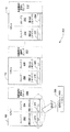
本開示および図を通して、同じ番号を同様の構成要素および機能を示すために使用する。100番代の番号は本来図1で見られる機能を指し、200番代の番号は本来図2で見られる機能を指し、300番代の番号は本来図3で見られる機能を指しており、以下同様である。 Throughout this disclosure and figures, the same numbers are used to indicate similar components and functions. The number in the 100s refers to the function originally seen in FIG. 1, the number in the 200s refers to the function originally seen in FIG. 2, and the number in the 300s refers to the function originally seen in FIG. The same applies hereinafter.
本開示は、データ生成タスクの並列実行のためのアーキテクチャおよび関連する技法に関する。こうしたデータ生成タスクは全般的に、第1組のデータを受信すること、次いでその第1組のデータに基づいて第2組のデータを生成することを伴う操作(operation)で、第2組のデータが第1組のデータよりも大量の情報を表す操作に関連する。第1組のデータと第2組のデータの比は、圧縮解除の比率を規定する。比較的高い圧縮解除比率を提供するアプリケーションは、背景技術の論述で定義したいくつかの問題に有効に対処することができる。例えば、比較的小さい1組の入力データから大量のデータを生成することができるアプリケーションでは、このデータを予め生成すること、システム・メモリに格納すること、およびその後こうしたデータを処理する時が来た場合にこのデータを取り出すこと、についての必要性を排除(または低減)する。したがって、こうしたアプリケーションは、システム・メモリとアプリケーションの処理モジュールとの間のデータの転送に関連付けられた有害な待ち時間および帯域幅の問題を回避することができる。さらに、こうしたアプリケーションは、限定されたリソースの場合が多く、特にゲーム・コンソールでは限定されたリソースとなるシステム・メモリに格納する必要がある情報の量を減らすこともできる。こうした改善により、ゲーム・コンソールの様々な構成要素に関連付けられたコストを低減することもできる。 The present disclosure relates to an architecture and related techniques for parallel execution of data generation tasks. Such a data generation task is generally an operation that involves receiving a first set of data and then generating a second set of data based on the first set of data. The data relates to operations that represent a larger amount of information than the first set of data. The ratio of the first set of data to the second set of data defines the decompression ratio. Applications that provide a relatively high decompression ratio can effectively address some of the issues defined in the background discussion. For example, in an application that can generate a large amount of data from a relatively small set of input data, it is time to pre-generate this data, store it in system memory, and then process such data. Eliminate (or reduce) the need for retrieving this data in some cases. Thus, such applications can avoid deleterious latency and bandwidth problems associated with the transfer of data between system memory and the application's processing module. In addition, such applications are often limited resources, and can reduce the amount of information that needs to be stored in system memory, which is a limited resource especially in game consoles. Such improvements can also reduce the costs associated with the various components of the game console.
グラフィカル・データに関するアプリケーション、音声データに関するアプリケーション、ビデオ・データに関するアプリケーションなどを含む、上記の設計戦略の多数のアプリケーションが想定される。ただし、説明を簡単にするため、以下の論述では、3次元コンピュータ・グラフィックスの分野、より具体的には3次元のゲーム関連のコンピュータ・グラフィックスの分野についての設計戦略のアプリケーションについて説明する。コンピュータ・グラフィックス・アプリケーションは、データ集中処理環境を表す。さらに、ゲーム・プレイング・コンソール環境では、かなり大量のデータを適時に処理する(例えばフレーム当たり16ミリ秒でシーンをレンダリングするなどの)必要があり、またこのデータを、通常比較的限られたシステム・メモリ・リソースを有するアーキテクチャを使用して処理する必要がある。したがって、3次元ゲーム・アプリケーションは、上記の設計戦略の理想的なアプリケーションを表している。しかし、上述のように、本明細書で記載するアーキテクチャおよび技法は、こうした例示のアプリケーションに限定されるものではないと解釈されたい。 Many applications of the above design strategy are envisioned, including applications related to graphical data, applications related to audio data, applications related to video data, and the like. However, for ease of explanation, the following discussion describes design strategy applications in the field of 3D computer graphics, more specifically in the field of 3D game-related computer graphics. Computer graphics applications represent a data intensive processing environment. In addition, game playing console environments require a fairly large amount of data to be processed in a timely manner (for example, rendering a scene at 16 milliseconds per frame), and this data is typically stored in a relatively limited system. It needs to be processed using an architecture with memory resources. Thus, the 3D game application represents an ideal application of the above design strategy. However, as noted above, the architecture and techniques described herein should not be construed as limited to such exemplary applications.
本開示は、以下の主なセクションを含む。セクションAでは、上記の設計戦略を実装する例示のシステムを説明する。セクションBでは、セクションAで論じたシステムの例示の操作方法(manner of operation)を説明する。セクションCでは、ゲーム・プレイング環境についてセクションAおよびBで説明したシステムおよび技法のアプリケーションについて説明する。 The present disclosure includes the following main sections: Section A describes an exemplary system that implements the above design strategy. Section B describes an exemplary manner of operation of the system discussed in Section A. Section C describes the applications of the systems and techniques described in Sections A and B for the game playing environment.
A.例示のシステムアーキテクチャ
A.1.システムの概要
図1は、レンダリングしたシーンで使用するより多くのジオメトリ・データを提供するシステム100の概要を示す。システム100は、パーソナル・コンピュータ(PC)、(Microsoft Corporation(Washington州、Redmond)によって製造されたMicrosoftのXbox(商標)ゲーミング・コンソールなど)ゲーミング・コンソール、または他の種類のプラットフォームなど、任意のプラットフォームに実装することができる。ジオメトリ・データとは、シーンをレンダリングするための3次元グラフィックス処理パイプラインで通常使用される情報を指す。通常のアプリケーションでは、データは、様々なキャラクタ、背景のオブジェクト、テクスチャなど、レンダリングされるシーンを構成する様々なオブジェクト(例えばモデル)を定義する、3次元グラフィックス処理パイプラインへの入力である。こうしたオブジェクトは、相互接続された多角形(ポリゴン)、通常は三角形、のメッシュとして表現される。各三角形は3つの頂点で構成される。この頂点は、頂点に関連する位置を識別する情報、ならびに頂点に関する他の情報(例えば色、テクスチャ座標、法線(normal)など)を収容する。例示の一実装形態では、単一の頂点に関連付けられた64バイトの情報がある。(説明を簡単にするため、本明細書では主に技法および実装形態について上記で定義したようなジオメトリ・データの処理/生成に関連して説明する。ただし、この技法および実装形態は、任意の種類のデータの処理/生成に使用できることを留意されたい。)
A. Exemplary System Architecture A. 1. System Overview FIG. 1 shows an overview of a
例示の一実装形態では、システム100は、フロント・サイド・バス106を介してグラフィックス処理装置モジュール104(以下、略して「GPUモジュール」104と呼ぶ)に接続されたコンピュータ処理装置モジュール102(以下、略して「CPUモジュール」102と呼ぶ)を備える。CPUモジュール102は、CPU1(108)、CPU2(110)、CPUn(112)(ここで、全般的に「n」は収集したCPUの最後のものを指す)など、任意の数のコンピュータ処理装置(CPU)の収集を含む。こうした複数のCPU(108、110、…112)は、グラフィックスゲーム開発者によって指定された一連のプログラム命令に基づいてデータを処理する汎用コンピューティング・ユニットを提供する。GPUモジュール104は、受信データに関する低レベル3Dグラフィックス処理タスクを実行するグラフィックス・エンジン114を備える。
In one exemplary implementation, the
図1の2つの主なモジュール、例えばCPUモジュール102およびGPUモジュール104を以下にさらに詳細に説明する。
The two main modules of FIG. 1, such as
CPUモジュール102から始めると、CPUモジュール102は、様々な役割をその複数のCPU(108、110、…112)に割り当てる。例えば、CPU1(108)は、ホスト処理装置として機能し、一方、CPU2からCPUn(110、…112)は、ジオメトリ処理装置として機能する。こうした役割に関連付けられたタスクは、様々なアプリケーション毎に異なる。通常のゲーミング・アプリケーションでは、ホストCPU1(108)は、プレーヤからの入力を受信し、シーンの管理を行い、アプリケーションによって示された物理現象をシミュレートするのに使用する計算を行い、ゲームによって提供される任意の人工知能を実行するなど、ゲームに関連付けられた高レベルのタスクを実行する。CPU2からCPUn(110、…112)は、ゲームに関連する、より細分化された(fine-grained)、処理を行う。一アプリケーションでは、こうした複数のCPU(110...112)は、シーン内の1つまたは複数のオブジェクトに関連するジオメトリ・データを生成する。例えば、以下に説明するように、こうしたプロセッサはそれぞれ手続き型ジオメトリを生成する論理を含むことができる。こうした論理は、実行すべきタスクを定義づける入力データを受信し、次いでこうしたタスクを実行して出力ジオメトリ・データ(例えば頂点の収集体(correction))を提供する。単に一例を挙げれば、ゲーム設計者は、木の個々の葉に関連付けられたジオメトリ・データを生成する手続き型論理を提供することができる。こうした手続き型論理は、個々の葉の位置、シーン内の任意にシミュレートされた風の方向などの、タスクに関連付けられた比較的限定された量の情報を受信する。この情報に基づいて、手続き型論理は、木の個々の葉を定義づける頂点を生成することができる。ジオメトリに関連するタスクを実行するCPUを、ジオメトリ生成CPUと呼ぶ。
Starting with the
他のアプリケーションでは、ジオメトリ生成CPU2からCPUn(110、…112)は、高次の表面のテセレーションを行うことができる。高次の表面とは、三角形の単純なメッシュではなく、他のパラメトリック形式でオブジェクトを表すことを指す。しかし、大抵の3次元処理エンジンは、三角形などの、単純な多角形として表されたオブジェクトしか処理しない。テセレーションのプロセスでは、こうした高次表面を三角形など、より基本的な多角形に分割する。したがって、ジオメトリ生成CPU2からCPUn(110、…112)は、こうしたテセレーションを行うために、すなわち、高次表面を受信し、この表面をより基本的な形に分割するために使用することができる。例示の高次表面は、Bスプライン面、ベジェ面、n−パッチなどを含む。 In other applications, geometry generation CPU2 through CPUn (110,... 112) can perform higher order surface tessellation. Higher-order surfaces refer to representing objects in other parametric forms rather than simple triangular meshes. However, most 3D processing engines only process objects that are represented as simple polygons, such as triangles. The tessellation process divides these higher-order surfaces into more basic polygons such as triangles. Thus, the geometry generation CPU2 to CPUn (110,... 112) can be used to perform such tessellation, i.e., receive higher order surfaces and divide the surfaces into more basic shapes. . Exemplary higher order surfaces include B-spline surfaces, Bezier surfaces, n-patches, and the like.
ジオメトリ生成CPU2からCPUn(110、…112)は、詳細レベル(level-of-detail:LOD)処理と併せて、上述の手続き型ジオメトリおよび/または高次の表面テセレーションを提供することができる。LOD処理では、シーン内のオブジェクトに関連付けられた複雑性のレベル(および、それによるジオメトリ・データ)は、ビューアーとシーン内の任意のオブジェクト(または任意のサブ・オブジェクト部分)との間の距離の関数として変化する。LOD処理は、様々な圧縮比率を適用して様々な複雑性レベルを達成することができる。これは、より高い詳細レベルで、ビューアーに「近い」オブジェクトにより高レベルの圧縮解除を適用するという効果をもたらす。 Geometry generation CPU2 through CPUn (110,... 112) can provide the procedural geometry and / or higher order surface tessellation described above in conjunction with level-of-detail (LOD) processing. In LOD processing, the level of complexity associated with an object in the scene (and thus the geometry data) is the distance between the viewer and any object (or any sub-object part) in the scene. It changes as a function. LOD processing can achieve different levels of complexity by applying different compression ratios. This has the effect of applying a higher level of decompression to objects that are “close” to the viewer at a higher level of detail.
上記で提供した例は、ジオメトリ・データ(例えば色、テクスチャ座標、法線(normals)など)の生成に関する。ただし、CPU2からCPUn(100、…112)を使用して、GPUコマンドなど他の種類のデータを手続き型として生成することができる。
The examples provided above relate to the generation of geometry data (eg color, texture coordinates, normals, etc.). However, other types of data such as GPU commands can be generated as procedural
n個のCPU(108、110、…112)を図1で示したが、上述のように、(例えば2つだけのCPUの場合も含めて)任意の数のCPUを備えることができる。さらに、追加のCPUをホストに関連した機能の実行に充てることができる(すなわち2つ以上のCPUをホスト関連の機能の実行に割り当てることができる。)。一実装形態では、CPU(108、110、…112)はすべて同様に構成される。すなわち、CPUはすべて同一の命令セットを使用して動作するが、ゲーム開発者が提供したプログラムに基づいて異なる機能を実行する。例えば設計者は、CPUモジュール102の試験、およびゲーム開発者による後のCPUモジュール102のプログラミングを容易にするためにCPUモジュール102のCPUがすべて同じ構成を持つように、CPUモジュール102を設計することを選ぶことができる。ただし他の実装形態では、1つまたは複数のホストCPUを、ジオメトリ生成CPUとは異なるアーキテクチャおよび機能性を有するように設計することができる。
Although n CPUs (108, 110,... 112) are shown in FIG. 1, as described above, any number of CPUs (including, for example, only two CPUs) can be provided. In addition, additional CPUs can be devoted to performing host-related functions (ie, more than one CPU can be assigned to perform host-related functions). In one implementation, the CPUs (108, 110,... 112) are all similarly configured. That is, the CPUs all operate using the same instruction set, but perform different functions based on the program provided by the game developer. For example, the designer may design the
一適用例では、CPU(108、110、…112)に静的に役割を割り当てるように、例えばCPUにホストCPUまたはジオメトリ生成CPUの役割を割り当てるように、システム100を構成ことができる。他の適用例では、システム100にこうした役割を、できればフレーム・ベース単位でフレーム毎に、または1つのフレーム内で(例えばイントラ−フレーム(intra-frame)ベースで)何回も動的に割り当てることができる。したがって、一適用例では、CPU(108、110、…112)すべてにホスト関連のタスクを処理する役割を割り当てることができる。このことは、プログラマがジオメトリ生成CPU2およびCPUn(110、…112)によって提供される特別の機能を役立てることを望まない場合に適している。場合によっては、システム100は、ジオメトリに関連する処理の役割をフレーム時間の一部でCPU(108、110、…112)すべてに割り当てることができる。また場合によっては、以下に論じるように、システムは1つまたは複数のCPUモジュール102を備えることができる。この場合、システム100は、(ジオメトリ処理など)同じ役割を1つのCPUモジュール102内のCPUすべてに割り当てることができる。このシナリオでは、ホスト処理の役割を割り当てたCPUモジュール102をシステム・メモリ130に最も近接して配置することが有益であると考えられる。(なぜなら、環境によっては、ホストが、ジオメトリ処理機能よりもランダムアクセス読取りミスによって有害な衝撃を受ける可能性が高く、したがって、ジオメトリ処理機能よりも待ち時間を短縮する必要があるからである。)
In one application, the
各CPUは内部L1キャッシュを備える。例えば、CPU1(108)は内部L1キャッシュ116を備え、CPU2(110)は内部L1キャッシュ118を備え、CPUn(112)は内部L1キャッシュ120を備える。キャッシュとは、CPUに使用される可能性が高いデータを格納する、容易にアクセス可能な記憶空間(readily accessible storage space)を指す。L1キャッシュ(116、118、…120)は、図で示していないが、従来の方法で、命令関連の情報の格納に割り当てられる部分、データの格納に割り当てられる部分を含む。さらに、これも図で示していないが、各CPU(108、110、…112)は、記憶レジスタの収集体(correction)を備える。記憶レジスタは、L1キャッシュ(116、118、…120)よりもさらに容易にアクセス可能な記憶場所を提供する。
Each CPU has an internal L1 cache. For example, CPU 1 (108) includes an
CPU(108、110、…112)は、それぞれバス・インターフェース・ユニット124、126、および128を介した複数のポートを通って共有L2キャッシュ122に結合される。その名が示すように、各CPU(108、110、…112)は、L2キャッシュ122を共有する(例えば使用する)。図1で示したメモリの階層の説明を完全にすると、システム100はシステム・メモリ130を備える。このシステム・メモリ130は、(一例では、キロバイトの範囲またはメガバイトの範囲などの記憶容量を有する)ランダム・アクセス・メモリ(RAM)記憶装置を提供する1つまたは複数の記憶装置を備える。GPUモジュール104は、メモリ・コントローラ132を介してシステム・メモリ130と対話する。
The CPUs (108, 110,... 112) are coupled to the shared
L2キャッシュ122は、個々のL1キャッシュ(116、118、120)と同様に、CPU(108、110、…112)およびGPUモジュール104によって要求される可能性が高い情報を格納する。すなわち、これらのキャッシュ(116、118、120、122)は、システム100の処理機能が、システム・メモリ130から読取りまたはそれに書き込む必要なくデータにアクセスできるようにする。システム・メモリ130からの読取りまたはそれへの書込みは、待ち時間の遅延をもたらす(例えば例示の一実装形態では、100サイクルを超える遅延の可能性がある)ため、こうした操作を回避することは一般に望ましいことである。しかし、データがキャッシュ(116、118、120、122)の1つから得られない場合は、システム100の処理機能は、システム・メモリ130内のこうしたデータにアクセスする。図4および5に関連してさらに詳細に説明するように、共有L2キャッシュ122は、n−ウェイ・セット・アソシアティブ(n-way set associative)キャッシュとして実装することができる。物理的実装に関しては、一例では、L2キャッシュ122は、キロバイト範囲またはメガバイト範囲などの全メモリ容量を有するRAMメモリの収集体を備えることができる。
Like the individual L1 caches (116, 118, 120), the
CPUモジュール102は、さらに、クロスバー結合機構134(以下では略して単にクロスバー134と呼ぶ)を備える。このクロスバー134は、複数の入力ポートの任意の1つを複数の出力ポートの任意の1つに選択的に接続する切替機構を備える。クロスバー134の実装には、多重化機構を使用するなど、様々な方法がある。
The
クロスバー134は、I/Oインターフェース138を介したI/Oモジュール136など、いくつかのエンティティへの接続性を提供する。I/Oモジュール136は一般に、特定のアプリケーションに接続して、入力を受信し、かつ/または出力を提供する任意の機能を示す。ゲーム・アプリケーションでは、I/Oモジュール136は、Universal Serial Bus(USB)機構などを介した様々なコントローラを使用して、ゲーム・プレーヤからの入力を受信することができる。このI/Oモジュール136は、ネットワーク接続性(network connectivity)、音声システム結合なども提供することができる。
クロスバー134は、対称型多重処理(Symmetric Multiprocessing(SMP))インターフェース142を介して他のCPU処理モジュール140へのオプションの接続性も提供する。対称型多重処理とは、複数のCPUが同じメモリ・スペースおよびオペレーティング・システムを共有する構成(arrangement)を指す。このような機能が特定のアプリケーションに望ましいと判断された場合に、任意選択の他のCPUモジュール140はその付加的な処理パワーをシステム100に提供する。
The
クロスバー134は、また、GPUインターフェース144およびCPUインターフェース146を介してGPUモジュール104に接続性を提供する。フロント・サイド・バス106は、GPUインターフェース144とCPUインターフェース146を結合する。バス106は、ジオメトリ生成CPU2からCPUn(110、…112)によって生成される大量データを処理するための十分な帯域幅、ならびにホスト帯域幅およびコヒーレンシ・トラフィック(coherency traffic)を有する必要がある。GPUモジュール104内の別のクロスバー148は、CPU2からCPUn(110、…112)から受信したジオメトリ・データ(ならびに他のデータ)をグラフィックス・エンジン114に向ける。グラフィックス・エンジン114は、多様なグラフィックス関連の操作を行うことができる。こうした操作は、(通常、頂点データを幾何学的に変換し、頂点データにライティング、例えばシェーディングを与える)頂点処理、背面の除去(backface culling)処理、クリッピング処理、三角形セットアップ処理、ラスタ化、ピクセル・ベースのシェーダ処理、フォグ処理、アルファ・テスト、深度テスト、ステンシル・テスト、アルファ・ブレンディング、ディザリングなどを含む、従来の3次元グラフィックス処理パイプラインに関連した様々なタスクを含むことができる。従来のグラフィックス・パイプライン処理の例示の概要は、文献(例えば、非特許文献1)に記載されている。例示の一実装形態では、CPU(108、110、…112)は、GPUモジュール104によって提供される機能とはいくつかの点で異なる。例えば、CPU(108、110、…112)は通常、GPUモジュール104よりも、はるかに多くの汎用ソフトウェア・プログラミングモデルを有し、単一のスレッド化アプリケーションではるかに良好に機能し、より多くの判断に基づいた分岐を可能にする。他の実装形態では、CPU(108、110、…112)が提供する機能とGPUモジュール104が提供する機能の差は少ないと言うことができる。
以下のセクションBで論じるように、例示の一実装形態では、GPUモジュール104は、ダイレクト・メモリ・アクセス(DMA)プロトコルを使用してメモリと対話する。例えば、システム100は、DMA機構を使用してコマンド・リスト取出し(fetch)を行う。このDMA機構は、データがどこから入手されたか「知らない」。データを正確な位置から取り出すのはクロスバーの機能であるためである。一実装形態では、システム100は、フロント・サイド・バス106を介してデータを取り出すために、CPUモジュール102からの「読取り」を開始する特定のパケットを生成する。
As discussed in Section B below, in one exemplary implementation, the
コヒーレンシ・モジュール150は、CPUキャッシュ常駐データがメイン・メモリとコヒーレントのままであることを任意選択で保証する。コヒーレンシ・モジュール150は、システム100によって提供されるデータ・ストリーミングに特に適合された機能も提供するが、こうした機能は、伝統的なキャッシュ・コヒーレンシとは1つまたは複数の点で異なる。コヒーレンシ・モジュール150の動作に関するさらなる詳細を以下にセクションBで述べる。
例示の一実装形態では、CPUモジュール102は、ゲーム・プレイング・コンソールで第1のチップとして実装され、GPUモジュール104はゲーム・プレイング・コンソールで第2のチップとして実装される。追加のCPUモジュール・チップを、関連するGPUモジュール・チップと共に含むことができる。他の実装形態では、図1で示した機能を図1で示したものとは異なる方法で共にグループ化することができる。
In one exemplary implementation, the
A.2.マルチ−スレッド化
図1では、各CPU108、110、112の全体のそれぞれが、ホスト関連処理の単一スレッド、またはジオメトリ生成処理の単一スレッドに充てられている。しかし、図2は、CPU(108、110、…112)内の処理リソースを複数のスレッド(例えば、2つ以上のスレッド)に割り当てる構成200を示している。すなわち、CPU1(108)は、ホスト関連処理に充てた複数のスレッド(202、204、…205)を含む。CPU2(110)は、ジオメトリ関連処理に充てた複数のスレッド(206、208、…209)を含む。CPUn(112)は、ジオメトリ関連処理に充てた複数のスレッド(210、212、…213)を含む。他の実装形態では、単一のCPUに関連付けられた役割をホスト関連の処理とジオメトリ関連の処理(または他の種類の処理)に分割することができる。例えば、CPU1(108)のスレッド202をホスト関連の処理に充て、スレッド204をジオメトリ関連の処理に充てることができる。一実装形態では、細分化ハードウェア・スレッド化技法を使用してマルチスレッド化を実装することができる。
A. 2. Multi-Threading In FIG. 1, each of the
一般に当技術分野で周知のように、スレッドとは、処理装置によって実行されるタスクを指し、通常、一連のサブタスクを備え、このサブタスクはこうしたサブタスクのシーケンスを形成する特定の順序で実行される。2つのスレッドを収容する例示の処理装置は、2つのこうしたタスクの間でリソースを割り当てる。例えば、一例では、処理装置は、複数のサブタスクを含む第1のタスク(スレッド)を実行することができる。こうしたサブタスクの実行中に、データ・ハザードに遭遇した場合は、サブタスクの処理に遅れが生じる。例えば、データを即時にアクセス可能なキャッシュの位置から得ることができない場合、システムは、システム・メモリ130などあまり簡単にアクセスできないソースからデータを取り出さなければならない。この操作は、第1のスレッドの実行に数百サイクルの可能性がある遅延をもたらすことがある。こうした遅延は、第1のスレッドの実行における「バブル」を表現するものである。処理装置がこのバブル中にアイドル状態にならないように、処理装置は、処理装置のアイドル・リソースを使用して第2のスレッドのサブタスクを実行するように構成される。こうすると、処理装置は、そのリソースをより有効に使用し、また潜在的にシーンのレンダリングを促進する。
As is generally known in the art, a thread refers to a task that is performed by a processing device and typically comprises a series of subtasks that are executed in a particular order that forms a sequence of such subtasks. An exemplary processing device that accommodates two threads allocates resources between two such tasks. For example, in one example, the processing device can execute a first task (thread) including a plurality of subtasks. If a data hazard is encountered during execution of such a subtask, processing of the subtask is delayed. For example, if the data cannot be obtained from a cache location that is immediately accessible, the system must retrieve the data from a source that is not very easily accessible, such as
図2で示した構成200では、各スレッドはそれ自体のL1キャッシュ(または1つのL1キャッシュのそれ自体の部分)を含む。例えば、各CPUが2つのスレッドを備える例示の場合では、構成200は、L1キャッシュ214、216、218、220、222、および224を備える。他の実装形態では、CPUの各スレッドは共通のL1キャッシュを使用する。この構成は図2で示され、スレッド202、204などに単一のL1キャッシュ226を例示的に提供することで示している。
In the
図では示していないが、GPUモジュール104も1つまたは複数のスレッドを使用して、割り当てられたタスクを実行することができる。
Although not shown in the figure, the
さらに、(例えば図5を参照する)以下の論述では、複数のCPUを使用し、各CPUが複数のスレッドを含むことができる例を示す。ただし他の実装形態では、CPUモジュールは、複数のスレッドを有するCPUを1つだけ使用することができる。この単一のCPUのシナリオでは、ホストの役割を果たす1つまたは複数のスレッドを提供し、ジオメトリ・データを生成する役割を果たす1つまたは複数のスレッドを提供することができる。一般用語「処理要素」は、本明細書では広範な機能(connation)を有し、例えば、単一スレッド化CPUまたはマルチスレッド化CPUに実装されたスレッド、あるいは他の種類の処理機能を指すことができる。 Further, the following discussion (see, eg, FIG. 5) shows an example where multiple CPUs are used, and each CPU can include multiple threads. However, in other implementations, the CPU module can use only one CPU having multiple threads. In this single CPU scenario, one or more threads acting as a host can be provided and one or more threads acting as generating geometry data can be provided. The general term “processing element” has a wide range of functions in this specification and refers to, for example, a thread implemented on a single-threaded CPU or a multi-threaded CPU, or other types of processing functions. Can do.
A.3.帯域幅の考察
図3は、ジオメトリ関連のタスクに充てたCPU2からCPUn(110、…112)を使用したジオメトリ・データの生成、ならびに、これらのユニット(110、112)に供給されたデータ量に対して、これらのユニットが供給するジオメトリ・データ量を測定した結果の圧縮解除の比率を、示すものである。より具体的には、CPU2(110)は、(詳細レベル(level-of-detail)の処理と共に)手続き型ジオメトリ論理または高次表面テセレーション論理など、データ生成論理302を含む。同様に、CPUn(112)は、(詳細レベルの処理と共に)手続き型ジオメトリ論理または高次表面テセレーション論理データ生成論理304を含む。論理302に与えられる入力データを比較的細い矢印306で示し、論理302によって生成される出力データを比較的太い矢印308で示す。これは、上記で強調した概念を示すものであって、すなわち、論理302は比較的少量のデータを受信し、それに反応して比較的大量のジオメトリ・データを生成することを示している。(細い矢印306で示した)入力データと(太い矢印308で示した)出力データの比を、論理302の圧縮解除比率と呼ぶ。こうした圧縮解除比率は一適用例では少なくとも1対10、他の適用例では少なくとも1対100、また別の適用例などでは少なくとも1対1000、またはそれより大きくてもよい。例えば、少なくとも1対100の圧縮解除が提供された場合は、入力データ量の出力データ量に対する比が少なくとも1/100であることを示す。CPUn(112)は、矢印310で示した入力データを受信し、矢印312で示した出力データを提供する。CPU2(110)についての論述は、CPUn(112)の機能にも当てはまる。CPU2(110)からCPUn(112)によって提供された出力データは、GPU処理モジュール104に供給され、例えば、従来の3次元グラフィックス処理パイプラインでさらに処理される。(上記の論述は、システム100の例示の利点を強調するために、比較的大きい圧縮解除比率に関連して構成されているが、例えば1対10など比較的小さい圧縮解除比率も可能である。)
A. 3. Bandwidth Consideration FIG. 3 shows the generation of geometry data using CPUn (110,... 112) from CPU2 devoted to geometry-related tasks, and the amount of data supplied to these units (110, 112). On the other hand, the ratio of decompression as a result of measuring the amount of geometry data supplied by these units is shown. More specifically, CPU 2 (110) includes
図1で提供したバスを、上記で論じた読取りの帯域幅(reading bandwidth)と書込みの帯域幅(writing bandwidth)の間の非対称性に対応するように適合させることができる。例示の一実装形態では、書込みの帯域幅を読取りの帯域幅の約2倍または3倍にすることによって、これを実装することができる。場合によっては、システム100は、圧縮解除比率1対100、または1対100、あるいはそれ以上を実現することができる。ただし、こうした比較的大きい圧縮解除比率は、手続き型ジオメトリ生成に関与する書込み動作のストリーミング中、または他の(データの圧縮解除に関与する、または関与しない)高帯域幅の書込み動作中のシステム100の動作を単に反映するだけである。したがって、それぞれ読取りと書込みの帯域幅の間にこうした大差がない場合は、読取りと書込みの帯域幅の間の比較的小さい比率(すなわち、約1対2、1対3などの比率)を提供して、他の処理モードに対応することができる(ただし、処理環境および他の考察によって、他の実装形態では、読取りの帯域幅に比べて比較的大きい書込みの帯域幅を提供することができる)。
The bus provided in FIG. 1 can be adapted to accommodate the asymmetry between the reading bandwidth and the writing bandwidth discussed above. In one exemplary implementation, this can be implemented by making the write bandwidth about twice or three times the read bandwidth. In some cases, the
例示する一実装形態の全体では、これらのCPUは、特定のデータ処理環境の要件によって、秒当たり数千または数百万の頂点、または秒当たり別の量の頂点のジオメトリ・データの集合体ストリームを生成することができる。例示の一実装形態では、頂点当たり数バイト(例えば32、64、128など)の非圧縮データを使用するが、これはCPUモジュール102からGPUモジュール104へのMB/sまたはGB/sの帯域幅に相当する。しかし、これより小さい、または大きいレートを提供することもできる。
In one exemplary implementation as a whole, these CPUs are aggregate streams of thousands or millions of vertices per second, or another amount of vertices of geometric data per second, depending on the requirements of a particular data processing environment. Can be generated. One exemplary implementation uses several bytes per vertex (eg, 32, 64, 128, etc.) of uncompressed data, which is the MB / s or GB / s bandwidth from the
上述の高レベルの圧縮解除にはいくつかの利点がある。例えば、ゲーム・コンソールの場合は、高レベルの圧縮解除を提供することは、(例えば待ち時間の短縮によって)コンソールの性能を向上させ、コンソールのシステム・メモリ要件(system memory requirements)(および関連するコスト)を低減させる。CPUモジュール102に高レベルの圧縮解除をもたらすことによって、ゲーム・コンソールの他の構成要素、システム・バス、配布媒体(例えばDVD)、周辺バス、ネットワーク接続などの複雑性および関連コストを低減することもできる。例えば、CPUモジュール102に適用される圧縮解除により、ゲーム・コンソールの他の構成要素で従来使用される圧縮/圧縮解除方式の複雑性および関連コストを低減することができ、または場合によって、こうした伝統的圧縮方式をなくすこともできる。
The high level of decompression described above has several advantages. For example, in the case of game consoles, providing a high level of decompression improves console performance (eg, by reducing latency) and improves console system memory requirements (and related Cost). Reduce complexity and associated costs of other components of the game console, system bus, distribution media (eg, DVD), peripheral bus, network connection, etc. by providing a high level of decompression to the
A.4.L2キャッシュ
図4および5は、図1で示したL2キャッシュ122の構成および動作に関する、さらなる詳細を提供するものである。例示の一実装形態では、図4から開始して、L2キャッシュ122は、n−ウェイ・セット・アソシアティブ・キャッシュとして実装され、一実装形態では、nは16以下でもよい(ただし、他の実装形態では16セットよりも多いセット・アソシアティブ・キャッシュを使用することができる)。より具体的には、L2キャッシュ122は複数のセット(402、404、406、…408)を含む。各セットは、それに関連付けられた様々なフィールドを有する複数のキャッシュ・ラインを含む。第1のフィールド410は、特定のラインに提供された情報が有効か無効かを示す有効性ビット(validity bit)を提供する。第2のフィールド412は、アドレス・マッチングのために使用するタグ情報を提供する。第3のフィールド414はデータを提供する。従来の論理要素のグループは、アドレス416をL2キャッシュ122のエントリと突合せ、その位置に格納されたデータを出力する。すなわち、アドレス416の指標(インデックス)部分418を使用して、L2キャッシュ122内の特定のキャッシュ・ライン420を識別する。アドレス416のタグ部分422は、L2キャッシュ122のフィールド412に格納されたタグ情報と、指標部分418によって識別されたキャッシュ・ライン内のタグ部分422とを比較することによって、システム100がL2キャッシュ122内のデータの特定部分を識別できるようにする。比較要素424、426、428、および430は、こうしたタグ比較機能を実行する。要素432、434、436、および438は、L2キャッシュ122内の一致した位置に格納されたデータを転送する。
A. 4). L2 Cache FIGS. 4 and 5 provide further details regarding the configuration and operation of the
図5は、図4で示した各セットを様々な処理スレッド(202〜213)に割り当てることができる方法を示す。これらの処理スレッド(202〜213)およびその構成の機能については図2を参照して論じたので、ここでは再び説明しないが、各CPU(108、110、…112)は2つ以上のスレッドを使用することができることを指摘する。ただし、論述を簡単にするために、各CPUのスレッドのうち2つだけが提供された機能を以下に説明する。上述のように、例示の一実装形態では、L2キャッシュ122は(一例では16以下などの)n−ウェイ・セット・アソシアティブ・キャッシュとして実装される。したがって、図5は、n個のセットのラベル付きセット1からセットnを示す。
FIG. 5 illustrates how each set shown in FIG. 4 can be assigned to various processing threads (202-213). These processing threads (202-213) and the function of their configuration have been discussed with reference to FIG. 2 and will not be described again here, but each CPU (108, 110,... 112) has two or more threads. Point out that it can be used. However, in order to simplify the discussion, the function provided by only two of the threads of each CPU will be described below. As described above, in one exemplary implementation,
序論として、図1で示したシステム100は、書込みデータ・ストリーミング・モードで動作することができ、ジオメトリ生成タスクに割り当てられたCPUは大量のジオメトリ・データを生成する。CPUモジュール102は、この大量ジオメトリ・データをCPUモジュール102からGPUモジュール104にフロント・サイド・バス106を介して転送する。L2キャッシュ122は、ジオメトリ・データをGPUモジュール104に転送する前にバッファリングすることによってこの動作モードを容易にする。より具体的には、書込みストリーミング動作モードで、システム100は、1セットのL2キャッシュ122をロックし、このロックしたセットを使用してジオメトリ・データのGPUモジュール104への転送を容易にする。図5は、こうしたロックされたセット502を示し、L2キャッシュの残りのセットはアンロック状態のままである(アンロック・セット504と呼ぶ)ことを示す。システム100は、ホスト関連の役割に関連するスレッド202および204をアンロックされたセット504に割り当て、書込みストリーミングを実行する目的で、スレッド206〜212をロックされたセット502に割り当てる。換言すれば、スレッド202および204は、書込みストリーミング・データの生成には直接的役割を果たさず、したがってロックされたセット502と関連づけられていない。スレッド206〜212は、書込みストリーミング以外の様々な目的でアンロックされたセット504にアクセスすることもできる。例えば、例示の一実装形態では、スレッド206〜212は、アンロックされたセット504内のデータがデータに関連付けられた低帯域幅を有し、複数のスレッドによって再び読み出される可能性が高い場合は、そのデータへのアクセスが許可される。以下で説明するように、高帯域幅の動作時に、スレッド206〜212がアンロックされたセット504へアクセスすること可能にすることは、ホストスレッド202および204の性能を低下させる潜在的な負の効果をもたらし、したがって、禁止される。
As an introduction, the
様々な戦略を使用してロックされたセット502を提供することができる。例えば、キャッシュ・ラインは、通常、(読取りまたは書込み動作で)キャッシュ・ラインがどの程度最近アクセスされたかに関する判定など、様々な要因に基づいてキャッシュからキャスト・アウト(cast out)される。したがって、セット502は、ロックされたセット502内のエントリが常にごく最近アクセスしたL2キャッシュ122内のエントリであることを示すように、キャッシュ管理論理(図示せず)を構成することによってロックすることができる。これによって、こうしたエントリがリタイアする(例えば「キャスト・アウトされる」)のが阻止される。同じロッキング機能を果たす他の戦略もある。
Various strategies can be used to provide the locked set 502. For example, a cache line is typically cast out of the cache based on various factors, such as a determination as to how recently the cache line was accessed (in a read or write operation). Thus, set 502 is locked by configuring cache management logic (not shown) to indicate that the entry in locked set 502 is always the most recently accessed entry in
複数の先入れ先出し(FIFO)バッファ506、508、510、および512は、ロックされたセット502内に生成される。この例の場合は、4つのバッファが示してあるが、これよりも少ない、または多い数のバッファを提供することができる。こうしたバッファ(506、508、510、512)は、それぞれ複数の記憶要素を含み、それぞれジオメトリ生成処理スレッド(206、208、210、212)からデータを受信し、こうしたデータがGPUモジュール104によって取り出されるまでこのデータを格納する。すなわち、こうしたバッファ(506、508、510、512)は、スレッド(206、208、210、212)の書込み速度が通常GPUモジュール104の読取り速度と同期状態になく、したがってアクセスできるようになるまで処理スレッド(206、208、210、212)の出力を一時的に格納する機構が必要であることに対応するものである。より具体的には、各FIFO(506、508、510、および512)は、各FIFOに関連付けられた末尾ポインタ(tail pointer)(図示せず)を含む。この末尾ポインタは、GPUモジュール104のフィールドからのデータを読取りがどの程度進行したかをFIFOに関連するスレッドに通知する。この情報により、スレッドは、新規のジオメトリ・データを受けるためにFIFO内の記憶要素がどの程度解放されたかを判断することができるようになる。物理的実装に関して、一例では、ロックされたセット502はキロバイトの範囲の記憶容量を提供することができ、各FIFOは、その容量の一部を提供するが、他の実装形態では、これよりも小さい、または大きいFIFO記憶容量を提供することができる。
A plurality of first in first out (FIFO) buffers 506, 508, 510, and 512 are created in the locked set 502. In this example, four buffers are shown, but fewer or more buffers can be provided. Each of these buffers (506, 508, 510, 512) includes a plurality of storage elements, each receiving data from a geometry generation processing thread (206, 208, 210, 212), and such data is retrieved by the
各FIFOは、別個の開始位置および終了位置を有する。したがって、FIFOに関連するCPUは、FIFO内の格納位置を定期的に監視して、CPUがFIFOの末端部を越えてデータを格納しようとしないことを保証しなければならない。CPUがそれぞれのFIFO内の最後の格納位置に格納する場合、CPUは次のデータをそのFIFO内の最初の格納位置に、ラップ・アラウンドして(回り込んで)、格納しなければならない。このようにして、CPUはFIFOを循環バッファとして使用する。しかし、この技法の一欠点は、CPUがFIFOを介した進行を定期的に監視して、FIFOの末端部をオーバーシュートしないことを保証しなければならないことである。この検査を行うことは、ストリーミング書込み動作の複雑性を増加させ、またストリーミング書込み動作に潜在的に遅延をもたらす可能性がある。この問題に対処する一技法は、アドレスの中間部を使用してFIFO内にラップする(送り込む)ことである。例えば、スレッド212に関連するFIFO512について考察する。ラップすることは、アドレス514のトップおよびボトムのビットを無視することによって、FIFO512内で実行される。アドレス514のトップおよびボトム・ビットは、(図5でxで示したように)それぞれ「無視」ビット・フィールド516および518で示される。
Each FIFO has a separate start and end position. Therefore, the CPU associated with the FIFO must periodically monitor the storage location in the FIFO to ensure that the CPU does not attempt to store data beyond the end of the FIFO. If the CPU stores in the last storage location in each FIFO, the CPU must wrap around (wrap around) and store the next data to the first storage location in that FIFO. In this way, the CPU uses the FIFO as a circular buffer. However, one drawback of this technique is that the CPU must regularly monitor progress through the FIFO to ensure that it does not overshoot the end of the FIFO. Performing this check increases the complexity of the streaming write operation and can potentially introduce a delay to the streaming write operation. One technique to deal with this problem is to wrap (feed) in the FIFO using the middle part of the address. For example, consider the
L2キャッシュ122にロックされたセット502を提供する場合、ジオメトリ生成スレッド(206、208、210、212)の出力に関連付けられた書込みの高帯域幅が、L2キャッシュ122を「スラッシング(thrashing)」するのを防止することが望ましい。すなわち、ホスト関連のスレッド(202、204)は、従来のキャッシュに関連する目的でL2キャッシュ122の使用を、つまり、こうしたスレッド(202、204)によってアクセスされる可能性が最も高いデータを格納すること、を要求する。しかし、L2キャッシュ122内のセットをロックしない、キャッシュ・メモリに使用される置換え戦略を考慮すると、ジオメトリ生成スレッド(206、208、210、212)によって生成された大量のデータ書込みは、キャシュ122の外部にホストのデータを事実上キャストする(なぜならジオメトリ生成スレッドによって提供されたデータは、敏速に、ごく最近使用されたデータの位置を見込むからである)。これが生じると、ホスト関連の処理スレッド(202、204)は、システム・メモリ130など遠隔のメモリの中から、求められたデータにアクセスすることが必要になり、それによって処理の遅延が生じる。この有害な現象は上述の「スラッシング」に相当する。これが生じるのを防止するため、システム100は、ホスト関連の処理スレッド(202、204)の要求をジオメトリ生成スレッド(206、208、210、212)から分離する。このロッキング対策により、上記のスラッシングが防止される。さらに、ロックされたセットを使用せずに、ジオメトリ生成スレッドによって提供されるデータの一部もそれ自体キャッシュの外部にキャストされ、GPUがそれを使用することが可能になる前にシステム・メモリにラウンド・トリップさせる。大量データが生成されれば、許容不可能な帯域幅が要求されるようになる。そのためまた、GPUモジュール104を待たせることによって全体の性能を低下させる遅延が生じることになる。
When providing a locked set 502 to the
上記で述べたように、図1で示したシステム100は、CPU108、110、112に関連する役割を動的に割り当てることができる。同じように、L2キャッシュ122の構成を同様に動的に変更することができる。例えば、ゲーム開発者がジオメトリ生成CPU2からCPUn(110、112)によって提供される特別の機能の使用を望まない場合は、システム100はキャッシュ122全体をホスト関連の機能に割り当てることができる。あるいは、システム100は、2セット以上のL2キャッシュ122をストリーミング書込み動作に関与するジオメトリ関連のスレッドに割り当てることができる。
As described above, the
図6は、CPU処理モジュール602の他の実装形態を示す。図6で示したCPU処理モジュール602は、ホスト関連のCPU1(108)にそれ自体の専用L2キャッシュ604が設けられており、L2キャッシュ122をジオメトリ生成CPU(110、…112)と共有する必要がない点で、図1で示したCPU処理モジュール502と異なる。すなわち、図6の実装形態では、共有L2の122はCPU2からCPUn(110、…112)だけに結合されている。図6で示したこの構成では、ホスト関連のCPU108はそれ自体のL2キャッシュ604を有しており、したがって他のCPU(110、112)がこの専用L2キャッシュ604をスラッシングする可能性がないため、L2キャッシュ122内のセットをロックする必要がない。
FIG. 6 shows another implementation of the
A.5.命令セットの変更
図7および図8は、CPU(108、110、…112)で使用される論理になされた改善に関する。すなわち、通常、CPUはプログラミング命令ストックの規定のセットを使用してプログラミングできるように設計されている。こうしたプログラミング命令は、ロードおよび格納操作、算術演算、分岐操作などの組合せに関する。図7および8は、グラフィックス・アプリケーションで使用されるCPUアーキテクチャでよく見られる命令セットに対する2つの改善を示す。
A. 5). Instruction Set Changes FIGS. 7 and 8 relate to the improvements made to the logic used by the CPU (108, 110,... 112). That is, typically the CPU is designed to be programmable using a defined set of programming instruction stock. Such programming instructions relate to combinations of load and store operations, arithmetic operations, branch operations, and the like. Figures 7 and 8 show two improvements to the instruction set commonly found in CPU architectures used in graphics applications.
まず、図7は、ジオメトリ・データをCPU(108、110、…112)から出力する前に圧縮するのに使用する論理700を示す。上述のように、本開示で使用する用語、ジオメトリ・データとは主にシーンでレンダリングすべき表面を構成する三角形に関連する頂点情報を指す。論理700は、(処理ブロック702で示すように)非圧縮ジオメトリ・データを受信するステップ、(処理ブロック704で示すように)このジオメトリ・データを圧縮するステップ、および(処理ブロック706で示すように)圧縮したジオメトリ・データを出力するステップを含む。CPUの命令セットうちの1つまたは複数の命令は、論理700で示す一連の動作を開始させることができる。
First, FIG. 7 shows
一実装形態では、論理700は、第1のCPUレジスタ内に非圧縮ジオメトリ・データを受信するステップ、プログラムの命令によって指定されたように、このジオメトリ・データの圧縮を行うステップ、次いでこの圧縮ジオメトリ・データを他のCPUレジスタにロードするステップを含む。他の実装形態では、圧縮操作を、CPUから情報を出力することができる任意の機能に組合せることができる。
In one implementation,
圧縮自体に関しては、Microsoft Corporation of Redmond、Washingtonから提供されるMicrosoft(登録商標)DirectX(登録商標)9.(n)で使用される圧縮技法など、多様な周知の戦略を使用して、ジオメトリ・データを圧縮することができる。より具体的には、頂点に関連付けられた様々なタイプの情報を様々な技法を使用して圧縮することができる。さらに、頂点に関連付けられた様々なタイプの情報は、異なる圧縮比を受け入れることができる。例えば、最初のタイプの情報は、2対1の圧縮比で圧縮され、他のタイプは4対1などの圧縮比で圧縮されてもよい。この意味で、論理700で提供される圧縮は、可変可能な圧縮を指す(すなわち、頂点内の様々なタイプの情報に対して可変であることを指す)。さらに、圧縮は、アプリケーションの必要性に応じて同じタイプの情報に対して可変でもよい。例えば、ジオメトリ座標をあるメッシュに対しては8ビット値に圧縮し、配置の密度(fineness of placement)が重要であると判断される場合は、他のメッシュに対しては16ビットまたは32ビット値に圧縮することができる。
Regarding the compression itself, Microsoft® DirectX® 9 from Microsoft Corporation of Redmond, Washington. Various well-known strategies can be used to compress the geometry data, such as the compression technique used in (n). More specifically, various types of information associated with vertices can be compressed using various techniques. Further, various types of information associated with vertices can accept different compression ratios. For example, the first type of information may be compressed with a compression ratio of 2: 1, and the other type may be compressed with a compression ratio such as 4: 1. In this sense, the compression provided in
CPU(108、110、…112)から出力されたジオメトリ・データの圧縮は、CPUモジュール102とGPUモジュール104の間で転送されるジオメトリ・データの帯域幅を縮小することに役立つ。さらに、ジオメトリ・データの圧縮により、L2キャッシュ122のロックされたセット502のFIFOが、より多くのジオメトリ・データを格納できるようになる。
Compression of the geometry data output from the CPU (108, 110,... 112) helps reduce the bandwidth of the geometry data transferred between the
他の実装形態では、命令セットは、CPUで受信される情報を圧縮解除する論理も含む。この圧縮解除もやはり、データの様々な部分が様々な技法で圧縮解除され、様々な程度の圧縮解除を受ける可能性があるという点で可変であると考えられる。圧縮解除は、レジスタ間の操作で実装され、またはCPUがデータを入力するために使用する任意の機能に統合することができる。後者の技法では、圧縮解除をCPUの通常のロード・サイクルの一部として統合することができる。この圧縮解除機能にはいくつかの利点がある。まず、圧縮/圧縮解除機能を対称にして、CPUがメモリ階層の様々なレベル(例えば、メイン・メモリ、読取り専用内容媒体、またはL1/L2キャッシュ)に格納された圧縮データを読取りおよび書込みができるようにする。様々なゲーム機能はしばしば、かなり後に(例えば、長い時間がたって、そのデータがCPUのキャッシュに残る可能性が非常に低くなってから)使用されるデータを生成する。このような場合、CPUによって生成されてCPUの他のゲーム機能によって後に使用されるための圧縮データは、メイン・メモリの占有スペースがはるかに少なく、メモリへの書込みの帯域幅がより小さく、メモリからの読取りの帯域幅がより小さくてすむ。こうした占有スペースおよび帯域幅の改善のすべては、より多くのデータを格納する能力をもたらし、かつ/または、より多くのデータを有効な態様で提供することによって、より良好なゲームの機能性をもたらすことができるようになる。 In other implementations, the instruction set also includes logic to decompress information received at the CPU. Again, this decompression is considered variable in that various parts of the data can be decompressed with various techniques and subjected to various degrees of decompression. Decompression can be implemented with register-to-register operations or integrated into any function used by the CPU to input data. With the latter technique, decompression can be integrated as part of the normal load cycle of the CPU. This decompression function has several advantages. First, the CPU can read and write compressed data stored at various levels of the memory hierarchy (eg, main memory, read-only content media, or L1 / L2 cache) with the compression / decompression function symmetrical. Like that. Various game functions often generate data that is used quite a while later (eg, after a long time, it is very unlikely that the data will remain in the CPU cache). In such a case, the compressed data generated by the CPU and later used by other game functions of the CPU has much less space occupied by the main memory, less bandwidth for writing to the memory, Less bandwidth to read from. All of these space and bandwidth improvements provide the ability to store more data and / or provide better game functionality by providing more data in an effective manner. Will be able to.
図8は、理解しやすくユーザにやさしい方法でドット生成操作を提供する他の論理800を示す。2つのグラフィックス関連ベクトルV1(X1、Y1、Z1、W1)、およびV2(X2、Y2、Z2、W2)の従来のドット・プロダクト積は以下のように形成される。ドット・プロダクト積=V1・V2=X1X2+Y1Y2+Z1Z2+W1W2
FIG. 8 shows another
より具体的には、最良の性能をもたらすために、多くの現在のCPUの命令セットは、より理解しやすくユーザにやさしいArray of Structure (AOS)手法ではなく、Structure of Arrays(SOA)手法を用いてドット積を実行することをユーザに要求する。後者の手法では、ドット生成の実行に使用されるオペランド・データをCPUによって提供された適切なレジスタにロードする。次いで、このオペランド・データを、CPUによって使用されるSOA手法に対応する方法で「回転(rotating)」させて処理する。すなわち、1つのベクトルに他を乗算するには、このSOA技法では、1×4ベクトルを有効に横に回転して4×1ベクトルを提供する。これは、ベクトル・データを格納するために各レジスタのレーンを1つだけ使用するため、レジスタ容量を非効率的に使用することになる。さらに、(いわゆる「かきまぜ(swizzling)」操作で完了する)ベクトルを横に回転する操作は、ベクトル・データの有意義な変換を行っていない(すなわち、データに関して数学的操作を何も行っていない)という意味で「空の」実行サイクルを必要とする。プログラマが自分のデータをAOS形式で維持できるようにすることで、最適化への取組みが非常にやさしくなる。対照的に、SOAは普通のデータ構成設計、およびApplication Program Interface(API)パラメータの受け渡し(passing)に適合しない。さらに、SOAは一般に、プログラマのSIMDベクトル数学的(math)命令の使用を複雑にする。論理800は、上記のAOS手法を用いてこうした欠点を克服するものである。(ただし、本システム100で使用するCPUは、SOA手法を使用してもドット生成を行うことができるように構成されており、したがってユーザは、AOS手法またはSOA手法を用いてドット生成を行う任意選択権が与えられる。)
More specifically, in order to provide the best performance, many current CPU instruction sets use the Structure of Arrays (SOA) approach rather than the more understandable and user friendly Array of Structure (AOS) approach. Request the user to perform a dot product. In the latter approach, operand data used to perform dot generation is loaded into the appropriate register provided by the CPU. This operand data is then "rotated" in a manner corresponding to the SOA technique used by the CPU for processing. That is, to multiply one vector by another, this SOA technique effectively rotates the 1 × 4 vector laterally to provide a 4 × 1 vector. This uses register capacity inefficiently because only one lane of each register is used to store vector data. In addition, operations that rotate a vector laterally (complete with a so-called “swizzling” operation) do not perform significant transformations of the vector data (ie, do not perform any mathematical operations on the data). In that sense, it requires an “empty” run cycle. By allowing programmers to maintain their data in AOS format, optimization efforts become very easy. In contrast, SOA is not compatible with normal data structure design, and Application Program Interface (API) parameter passing. In addition, SOA generally complicates the use of programmers' SIMD vector math instructions.
より具体的には、論理800は、(操作ブロック802で示したように)ドット生成の実行に使用されるオペランドを受信するステップ、(操作ブロック804で示したように)AOS手法を用いてドット生成を行うステップ、次いで(操作ブロック806で示したように)ドット生成の結果を出力するステップを含む。
More specifically,
B.例示の操作方法
図9〜11は、図1で示したシステム100の例示の操作方法を示す。より具体的には、図9〜11には、上述のジオメトリ・データ・ストリーミング機能に関連する操作の2つの態様(aspect)が示してある。図9は、ストリーミング動作に関連する読取り機能を示し、図10および11は、ストリーミング動作に関連する書込み機能を示すものである。これに関連して、「読取り」は情報を例示のジオメトリ生成CPUにロードすることを指す。ジオメトリ生成CPUは次いで、入力データに関する手続き型ジオメトリ(または他の処理)の実行を行って出力ジオメトリ・データを提供する。「書込み」は、こうしたデータをジオメトリ生成CPUからGPUモジュールに転送することを指し、またそれに関連するキャッシュ管理の事柄すべてに関するものである。
B. Exemplary Operating Method FIGS. 9-11 illustrate an exemplary operating method of the
読取りストリーミングおよび書込みストリーミングの動作(operations)を、図1で示したシステム100全体の操作の概要と共に以下にさらに詳細に説明する。
Read and write streaming operations are described in further detail below, along with an overview of the overall operation of the
B.1.読取りストリーミング
(読取りストリーミング動作を示す)図9から始め、手続き型ジオメトリ論理904(またはジオメトリ・データを生成する他の種類の処理論理)、レジスタ906、およびL1キャッシュ908を含む例示のCPU902を示す。L2キャッシュ910もこの図に示してある。読取りストリーム動作の目的は、入力情報を入力ソースから有効に受信することである。こうしたソースを図9で包括的にバス912として示す。バス912によって提供される情報は、(図1の)システム・メモリ130、ホストCPU、または他のソースに由来することができる。例えば、ゲーム環境で3次元シーンを生成する場合、入力情報は3次元グラフィックス処理パイプラインでレンダリングされるべきオブジェクトの位置、またはそのシーンの他の属性を表すことができる。
B. 1. Read Streaming (showing a read streaming operation) Beginning with FIG. 9, an
情報をCPU902にロードするために使用することができる様々な技法がある。パス914で示した一技法では、L1キャッシュ908は、n−ウェイ・セット・アソシアティブ・キャッシュ(例えば4−ウェイまたはそれより多いセット・アソシアティブ・キャッシュ)として実装される。この技法では、情報はL2キャッシュ910をバイパスしてL1キャッシュ908のロックされたセット内に直接受信される。次いで、この情報をL1キャッシュ908からレジスタ906に転送することができる。パス916で示した他の技法では、情報はレジスタ906に直接転送される。パス918で示した他の技法では、情報は、L2キャッシュ910のロックされたセットに転送され、その後、レジスタ906に転送される。また他の技法(図示せず)では、セットをロックせずに、情報を2ウェイまたはそれより多いL1キャッシュ内にストリーミングすることができる。好ましい実装形態では、任意の技法を用いて、CPU902は読取り情報を先取り(prefetch)する。すなわちCPU902は、使用の前にこの情報を要求する(つまり、CPU902は、このデータの約100あるいはそれ以上のサイクルなど、複数サイクルをデータの使用前に受信する。ただしこれよりも少ない先取りサイクルを使用することもできる)。先取りは、処理に望ましくない遅延をもたらす可能性があるデータ読取り機能停止の衝撃を低減することによって、ストリーミング動作を容易にする)。上述の技法は、特定の処理環境によって、様々な利点を提供することができる。例えば、L1キャッシュのセットのロッキングに関する技法は、そのL1キャッシュに関連付けられたCPUだけに影響を与え、一方、共有L2キャッシュのロッキングはこのキャッシュに結合されたCPUすべてに影響を与えることになる。
There are a variety of techniques that can be used to load information into the
上述の方法でL1キャッシュ908またはL2キャッシュ910をバイパスすることは、CPU902がL1キャッシュ908またはL2キャッシュ910からの入力情報を再び読み取る可能性が低いため、CPU902の動作に負の影響を与えない。したがって、L1キャッシュ908およびL2キャッシュ910は、CPU902に読み込む情報のコピーを格納する必要がない。換言すれば、CPU902が入力情報を再び読み取る可能性が低いため、L1またはL2キャッシュは、最近受信した情報の簡単にアクセス可能なコピーを、後の読取りに備えて提供する従来の役割を担う必要がない。こうしたキャッシュをバイパスすることは、再使用される可能性が高い他のデータ(ストリーミング動作に関連していないデータなど)をキャッシュの外部にキャストさせてしまうことが回避されるため、このことは望ましいことである。すなわち、キャッシュのバイパスにより、ストリーミング動作がキャッシュをスラシングするのが防止される。
Bypassing the
B.2.書込みストリーミング
図10は、書込みストリーミング動作(operations)1000を示す。この図は、手続き型ジオメトリ論理1004(またはジオメトリ・データを生成する他の種類の処理論理)、レジスタ1006、およびL1キャッシュ1008を有する例示のCPU1002を示す。CPU1002ならびにGPUモジュール1014に割り当てられたFIFO1012を含むL2キャッシュのロックされたセット1010が示してある。より具体的には、FIFO1012は、CPU1002によって転送されたジオメトリ・データを受信する。FIFO1012は、GPUモジュール1014が取り出すことができるジオメトリ・データの一時的レポジトリ(保管場所)としての働きもする。
B. 2. Write Streaming FIG. 10 shows write
データパス1016および1018は、書込みストリーミング動作で行われる動作を示す。ただし、こうした動作タスクが実行される前に、システム100はL2キャッシュのセット1010(または潜在的に2つ以上のセット)をロッキングする予備ステップを実行する。FIFOのセットアップには、ロックされたセット1010内のラインに有効かついわゆる「ダーティー」としてマークを付けることによって、キャッシュを適切にセットアップすることも含まれる。この操作には、タグおよびデータをロックされたセット内のキャッシュ・ラインに割り当てることも含まれる。この操作は、「ダーティー生成(create dirty)」手順と呼ばれ、システム・メモリ130への必須読取りアクセスを使用する読取りの割り当てを行わない。
L2キャッシュをロックし適切に開始させた後、書込みストリーミング動作は、ジオメトリ・データをCPU1002からL2キャッシュのロックされたセット1010のFIFO1012に(例えばL1キャッシュ1008をバイパスして)直接転送することによって進行する。これは、ジオメトリ・データを受信するFIFO1012内の格納位置に関連する適切なアドレス位置にジオメトリ・データを書き込むことによって行うことができる。この動作をデータパス1016で示す。L1キャッシュ1008をバイパスすることによって、手続き型ジオメトリ論理1004の高出力帯域幅がL1キャッシュ1008をスラッシングするのが防止される。L1キャッシュ1008をバイパスすることは、書込みストリーミング・データがCPU1002によって再び読取られる可能性が低いため(したがって、このデータのコピーをL1キャッシュ1008内に維持する必要がないため)、CPU1002の性能に負の影響を与えない。代替の一実装形態(図示せず)では、n−ウェイ・セット・アソシアティブ・キャッシュを使用して、L1キャッシュ1008を実装することができ、およびこうしたキャッシュで提供されるセットの1つをロックして書込みストリーミング動作がL1キャッシュ1008をスラッシングするのを防止することができる。
After the L2 cache is locked and properly started, write streaming operations proceed by transferring geometry data directly from the
FIFO1012が所定量のジオメトリ・データを格納した後、または情報の転送に関する他のいくつかの条件が満たされた後(例えば、ジオメトリを生成する所与のAPI呼び出しによって要求されたジオメトリがすべて完成されると)、システム100はGPUモジュール1014を起動(kick off)する。これは、GPUモジュール1014にFIFO1012からの情報の取出しを促す。より具体的には、GPUモジュール1014はDMAプロトコルを使用してFIFO1012から情報を取り出すことができる。このDMAプロトコルでは、GPUモジュール1014は、システム100によってそれに提供されたアドレスに応じてFIFO1012からデータのブロックを取り出す。ただし、従来のDMAは、通常、システム・メモリとI/Oデバイスの間での情報の転送を調整する。この場合、一例では、システム・メモリ130とこうしたデータの転送を行うことを回避することが望ましい。この目的で、GPUモジュール1014のコヒーレンシ・モジュール(例えば、図1で示したコヒーレンシ・モジュール150)が、GPUモジュール1014にデータをシステム・メモリ130からではなく、L2キャッシュのロックされたセット1010から取り出すことを命令する。GPUモジュール1014が、(情報がL2キャッシュから「キャスト・アウト」されるようにして)L2キャッシュのロックされたセット1010のFIFO1012から情報を読取った後、コヒーレンシ・モジュール150は、エントリが有効としてマーク付けされ、かつダーティーとしてマーク付けされたまま維持する。この方法では、CPU1002は、キャッシュ・ラインの所有権をシステム・メモリ130に渡たすことを許可せずに、この所有権を維持する。換言すれば、この動作は、キャッシュ・ラインの再割り当ての結果ではなく、FIFO1012は、CPU1002に割り当てられたままであり、ポインタがラップ・アラウンドしてFIFO1012のトップを指定した場合に補充(refill)することができる。
After the
図10で示していないが、CPUはL1キャッシュ1008およびL2キャッシュ1010の両方をバイパスして、システム・メモリ130に直接書込みストリーミングを行うことができる(これは「非一時的格納(non-temporal store)」動作と呼ばれる)。この動作は、任意選択でデータをより大きいブロックに収集し、次いでデータのこうしたブロックをバス106を介してシステム・メモリ130に送ることによって行うことができる。この動作は、CPUによって生成されたデータが(例えばGPUモジュール1014によって)直ちに読取られないことが予測される場合に望ましい。この環境では、データがL1およびL2キャッシュ(1008、1010)に転送された場合、このデータが読取られる前に結局キャッシュからキャスト・アウトされる可能性がかなり高い。さらに、場合によっては、こうしたデータをL1およびL2キャッシュ(1008、1010)に格納することは、こうしたキャッシュをスラッシングすることになる。こうしたことを考察すれば、L1およびL2キャッシュ(1008、1010)をバイパスして、データをシステム・メモリ130に直接ストリーミングすることが妥当である。一例では、ホストCPUのグラフィックス・ドライバ(図示せず)は、この技法を用いて、(「プッシュ・バッファ(push buffer)」としても周知の)GPUコマンド・リストを生成し、このコマンド・リストをGPUモジュール1014に転送することができる。この場合、システム・メモリ130に対する書込みストリーミングにより、キャッシュ(1008、1010)のスラッシングを防止することができる。
Although not shown in FIG. 10, the CPU can bypass both L1 cache 1008 and
最後に、上記の論述は、データ・ストリーミングを使用して圧縮解除論理(例えば手続き型ジオメトリまたは高次表面テセレーション)によって生成された大量データをCPUモジュールからGPUモジュールに転送することに重点を置いたものである。ただし、上記の技法を使用して、任意のデータ(すなわち、圧縮解除論理によって生成されたものではないデータ)をCPUモジュールからGPUモジュールに転送することもできる。 Finally, the above discussion focuses on transferring large amounts of data generated by decompression logic (eg procedural geometry or higher order surface tessellation) from the CPU module to the GPU module using data streaming. It is a thing. However, any data (ie, data not generated by decompression logic) can be transferred from the CPU module to the GPU module using the techniques described above.
B.3.末尾ポインタの考察
図10を参照すると、GPUモジュール1014がジオメトリ・データをL2キャッシュのロックされたセット1010のFIFO1012から受信した場合、それによってGPUモジュール1014は、CPU1002によるFIFO1012への追加のジオメトリ・データの転送のためにメモリ・スペースを開放する。図11は、GPUモジュール1014がCPU1002にこうした開放スペースを通知する技法を示す。
B. 3. Tail Pointer Consideration Referring to FIG. 10, when the
より具体的には、図11は、手続き型ジオメトリ論理1104(またはジオメトリ・データを生成する他の種類の処理論理)、レジスタ1106、およびL1キャッシュ1108を備えた例示のCPU1102を示す。L2キャッシュ1110ならびにGPUモジュール1112もこの図で示す。さらに、図11は、GPUモジュール1112が、ロックされたセット(図11で示していない)内のFIFOに関連付けられた末尾ポインタ1114を格納していることも示す。より具体的には、末尾ポインタ1114は、GPUモジュール1010が読み取ったばかりのFIFO内の格納位置を指し示す。
More specifically, FIG. 11 shows an
GPUモジュール1112は、この末尾ポインタをL2キャッシュ1110に転送することによって、末尾ポインタ1114の現在の値をCPU1102に定期的に通知する。図11で、この動作をパス1116で示す。末尾ポインタをL2キャッシュ1110に格納することにより、L1キャッシュ1108内の対応する末尾ポインタの位置が無効としてマーク付けされる。L1の位置の無効化は、L1のデータを、L2の位置の同じ物理的アドレスに対して加えられた変更に対して、コヒーレントに保持するキャッシュ・コヒーレンシ機能を使用して行われる。その後のCPU1102による末尾ポインタの位置のロードは、例えばL2キャッシュ1110に格納された、ごく最新の末尾ポインタのバージョンを取り出すことによって応じられる。代替実装形態では、GPUモジュール1112は、読取り待ち時間を短縮する解決法が望まれる場合は、末尾ポインタをCPU1102またはGPU1112に関連付けられた他のいくつかのキャッシュ可能な記憶装置に直接転送することができる。これとは大きく異なり、GPUモジュール1112は、通常のGPUの構成では、システム・メモリと対話するが、それには、L2キャッシュ1110内の末尾ポインタの位置が無効になった後に、再ロードするのにさらに長い待ち時間を要する。割り込みを使用してこのタスクを処理すると、待ち時間の点でさらに問題が生じることになる。
The
CPU1102は、L1キャッシュ1108に格納された末尾ポインタを定期的にポーリングして、FIFO(図示せず)に手続き型ジオメトリ論理1104によって生成されたジオメトリ・データを受信する十分なスペースがあるか否かを決定する。CPU1102に関連付けられたローカルメモリのポーリングは、システム・メモリ130のポーリングよりもはるかに効率的である。なぜなら、メイン・メモリのポーリングは内部CPUバス、CPU/GPUバス、GPUバス、およびメイン・メモリの帯域幅を無駄に使用するからである。ポーリングはL1のキャッシュ可能な末尾ポインタの位置でなされるため、ポーリングの帯域幅はすべて、CPU1102に対してローカルであり、システム内の他の場所の共有リソースを消費せず、システム・メモリに関与する他のポーリング戦略に関連付けられた待ち時間の問題を生じさせない。
The
B.4.システムの動作の概要
図12は、図1で示したシステム100によって行われる上述のストリーミング動作の概要を示す。図の左側は、CPUモジュール処理1202に関するものであり、すなわち、図1で示したCPUモジュール102で行われる動作を示す。より具体的には、ブロック1204、1206、および1208は、CPU110、CPU112など、図1で示した個々のCPUで行われる処理に関する。図の右側は、GPUモジュール処理1210に関するものであり、すなわち図1で示したGPUモジュール104(かつGPUモジュール1212として図12に再掲した)で行われる動作に関する。CPUモジュール処理1202で行われる動作はGPUモジュール処理1210で行われる動作と並列に行うことができる。さらに、(ブロック1204、1206、1208の)個々のCPUで行われる動作は互いに並列に行うことができる。(ストリーミング動作の論述を簡単にするため、図1で示したホストCPU108など、任意のホストCPUの役割を図12では省略してあることを留意されたい。)
B. 4). Overview of System Operation FIG. 12 shows an overview of the above-described streaming operation performed by the
CPUで行われる例示の動作を、ジオメトリ処理CPU1204を参照して説明する。こうした動作には、CPU1204への情報の読取りを行うステップ1214が含まれる。この情報は、手続き型ジオメトリ操作(または高次表面テセレーション)を実行するためのCPU1204で使用される比較的少量のデータを構成要素とすることができる。例えば、木をレンダリングする上述の例では、受信情報は木の様々な部分の位置、ならびにレンダリングしたシーンで葉を動かす任意のシミュレートした風の方向および速度に関するデータを構成要素とすることができる。ステップ1216は、(圧縮した形で情報を受信した場合は)受信情報を圧縮解除することを行わせる。ステップ1218は、受信情報に基づいて手続き型ジオメトリ(または高次表面テセレーション)の実行を行わせる。ステップ1218は、1組の出力頂点の生成が行われる。木の例の場合では、頂点は、個々のそれぞれの葉のレンダリングに使用する三角形のメッシュを構成する。さらに、ステップ1218で行われる演算は、図8で説明したAOS手法を用いたドット・プロダクトの実行を含むことができる。ステップ1220は、出力頂点を圧縮することを行わせる。ステップ1222は、圧縮した頂点をL2キャッシュ1224のロックされたセットの、CPU1204に割り当てられた、FIFOに転送する。
Exemplary operations performed by the CPU will be described with reference to the geometry processing CPU 1204. Such operations include
図12の右側にあるステップ1226で、GPUモジュール1212はL2キャッシュ1224に格納された頂点を読み取る。ステップ1228で、GPUモジュール1212は、GPUエンジン(例えば図1のエンジン114)での頂点処理のために頂点をディスパッチする。最後にステップ1230は、GPUモジュール1212が末尾ポインタに関する情報をCPUモジュール102のCPUに定期的に転送することを全般的に示す。GPUモジュール1212は、こうして受信した頂点を末尾ライトバック更新と並列に処理することができる。上述のように、この末尾ポインタは、GPUモジュール1212のL2キャッシュ1224に格納された情報の読取りがどの程度進行したかを示し、新規の頂点データで充填することができるL2キャッシュ1224内の使用可能な解放スペースを、CPUに通知する。
In
セクションBでの上記の論述では、データをキャッシュ・メモリからGPUモジュール104に転送する例示の技法を1つしか示していないが、他の技法を用いることもできる。例えば、上記の論述では、コヒーレンシ・モジュール150は、複製タグ格納方式(duplicate tag store scheme)を使用してストリーミング動作でデータの転送を調整する役割を担う。他の戦略では、システム100は、L2キャッシュ122のロックされたセット502のFIFO(506〜512)に別個のアドレス範囲を割り当てることができ、こうしたアドレスはシステム・メモリ130にマップされない。この手法では、システム100は、情報がL2キャッシュ122のロックされたセット502に格納されたことを、複製タグ記憶装置を調査して決定する必要がない。したがってこの手法では、コヒーレンシ・モジュール130は、ストリーミング書込みFIFO(506〜512)に格納されたデータ以外のデータすべてに関して、CPUモジュール102のキャッシュとシステム・メモリ130の間のコヒーレンシを維持するためだけに使用される。
Although the above discussion in Section B shows only one exemplary technique for transferring data from cache memory to
C.ゲーム環境への例示の適用例
図13は、上述の並列アーキテクチャおよび技法を実装するために使用することができる例示のゲーム・システム1300を示す。このシステムは、ゲーム・コンソール1302、およびコントローラ1304(1)および1304(2)で示した4つまでのコントローラを備える。ゲーム・コンソール1302は、内部ハードディスクドライブおよび携帯用媒体ドライブ1306を装備している。この携帯用媒体ドライブ1306は、光記憶ディスク1308で示したような、様々な形態の携帯用記憶媒体をサポートする。適合する携帯用記憶媒体の例には、DVD、CD−ROM、ゲーム・ディスク、ゲーム・カートリッジなどが含まれる。
C. Exemplary Application to Game Environment FIG. 13 illustrates an
ゲーム・コンソール1302は、その前面に4つのスロット1310を有して、4つまでのコントローラを支持するが、スロットの数および構成は変更することができる。電源ボタン1312および排出ボタン1314もゲーム・コンソール1302の前面に位置する。電源ボタン1312は、ゲーム・コンソールへの電力の切替えをし、排出ボタン1314は携帯用媒体ドライブ1306のトレイを開閉して、記憶ディスク1308を挿入し、取り出すことができるようにする。
The
ゲーム・コンソール1302は、A/Vインターフェース・ケーブル1320を介してテレビジョンまたは他のディスプレイ(図示せず)に接続される。電源ケーブル1322は、ゲーム・コンソールに電力を供給する。ゲーム・コンソール1302はさらに、ケーブルまたはモデム・コネクタ1324で示したように、内部または外部の追加のネットワーク能力を装備して、ローカル・エリア・ネットワーク(LAN)またはインターネットなど、ネットワークにアクセスしやすくなっている。
各コントローラ1304は、有線または無線インターフェースを介してゲーム・コンソール1302に結合される。図で示した実装形態では、コントローラはUSB(Universal Serial Bus)コンパチブルであり、シリアル・ケーブル1330を介してゲーム・コンソール1302に接続される。コントローラ1304は、多様なユーザ対話機構の任意のものを装備することができる。図13で示したように、各コントローラ1304は、2つの基本コントロール・レバー(thumbstick)1332(1)および1332(2)、方向性またはD−パッド1334、表面ボタン1336、および2つのトリガ1338を装備している。こうした機構は単に代表的なものであり、他の周知のゲーム機構を図13で示したものに代え、または追加することができる。
Each
メモリ・ユニット(MU)1340をコントローラ1304に挿入して追加の携帯用記憶装置を提供することができる。携帯用メモリ・ユニットは、ユーザがゲーム・パラメータを格納し、それを輸送して他のコンソールでプレイできるようにする。記載の実装形態では、各コントローラは、2つのメモリ・ユニット1340を収容するように構成されているが、他の実装形態では2つより多い、または少ないユニットを使用することができる。
A memory unit (MU) 1340 can be inserted into the
図で示していないが、ゲーム・システム1300は、図1で示したシステム100に対応する処理アーキテクチャを含むことができる。こうしたシステム100によって、高度の複雑性があり、それによって比較的高度の現実性のある実現可能なシーンを生成することができるようになる。これは、プレーヤのゲームに対する興味に加えて、実体験のように感じるゲーム環境を作り出す助けをする。
Although not shown, the
D.結論
データ生成タスクを並列に実行するアーキテクチャおよび関連方法を開示した。例示の一適用例では、このアーキテクチャおよび関連方法は、複雑で現実性のあるシーンをレンダリングする大量のジオメトリ・データを提供するものである。同時に、このアーキテクチャおよび関連方法は、システム・メモリのデータ転送動作の量を低減する方法も提供する。
D. Conclusion An architecture and related methods for executing data generation tasks in parallel have been disclosed. In one exemplary application, the architecture and related methods provide a large amount of geometry data that renders a complex and realistic scene. At the same time, the architecture and related methods also provide a way to reduce the amount of system memory data transfer operations.
本発明を、構成機能および/または方法のアクト(methodological acts)に特有の言語で記載したが、理解されるように、特許請求の範囲で定義した本発明は、記載の特定の特徴および活動に必ずしも限定されるものではない。むしろ、特定の特徴および活動は、特許請求の範囲に記載されている本発明の例示の実装形態として開示したものである。 Although the present invention has been described in language specific to constituent functions and / or methodological acts, it should be understood that the invention as defined in the claims relates to the specific features and activities described. It is not necessarily limited. Rather, the specific features and acts are disclosed as exemplary implementations of the invention as recited in the claims.
100 システム
102 CPUモジュール
104 GPUモジュール
106 フロント・サイド・バス
108 CPU1(例えばホスト)
110 CPU2(例えばジオメトリ)
112 CPUn(例えばジオメトリ)
114 グラフィックス・エンジン
116、118,120 L1キャッシュ
124、126,128 バス・インタフェース・ユニット
122 共有L2
130 メモリ
132 メモリ・コントローラ
134 クロスバー
136 I/Oモジュール
138 I/Oインターフェース
140 追加の1つまたは複数のCPUモジュール(任意選択)
142 対称型多重処理(Symmetric Multiprocessing(SMP))インターフェース
144 GPUインターフェース
146 CPUインターフェース
148 クロスバー
150 コヒーレンシ・モジュール
200 CPU内の処理リソースを複数のスレッドに割り当てる構成
202 スレッド1(例えばホスト)
204 スレッド2(例えばホスト)
205 任意選択の追加のスレッド
206 スレッド1(例えばジオメトリ)
208 スレッド2(例えばジオメトリ)
209 任意選択の追加のスレッド
210 スレッド1(例えばジオメトリ)
212 スレッド2(例えばジオメトリ)
213 任意選択の追加のスレッド
214、216,218、220、222、224 L1キャッシュ
226 両方のスレッド用の1つのL1
302 データ生成論理(例えば手続き型ジオメトリ)
304 データ生成論理(例えば手続き型ジオメトリ)
410 有効性
412 タグ
414 データ
416 アドレス
418 指標
420 特定のキャッシュ・ライン
422 タグ
502 ロックされたセット
504 アンロック・セット
506、508、510、512 FIFOバッファ
514 アドレス
516、518 「無視」ビット・フィールド
602 CPU処理モジュール
604 専用L2キャッシュ
902 CPU
904 手続き型ジオメトリ論理
906 レジスタ
908 L1キャッシュ
910 L2キャシュ
912 バス
1000 書込みストリーミング動作
1002 CPU
1004 手続き型ジオメトリ論理
1006 レジスタ
1008 L1キャッシュ
1010 L2のロックされたセット
1012 FIFO
1014 GPUモジュール
1102 CPU
1104 手続き型ジオメトリ論理
1106 レジスタ
1110 L2キャッシュ
1112 GPUモジュール
1114 末尾ポインタ
1300 ゲーム・システム
1302 ゲーム・コンソール
1304 コントローラ
1306 携帯用媒体ドライブ
1308 光記憶ディスク
1310 スロット
1312 電源ボタン
1314 排出ボタン
1320 A/Vインターフェース・ケーブル
1322 電源ケーブル
1324 モデム・コネクタ
1330 シリアル・ケーブル
1332 コントロール・レバー
1334 D−パッド
1336 表面ボタン
1338 トリガ釦
100
110 CPU2 (eg geometry)
112 CPUn (eg geometry)
114
130
142 Symmetric Multiprocessing (SMP)
204 Thread 2 (eg host)
205 Optional
208 Thread 2 (eg geometry)
209 Optional
212 Thread 2 (eg geometry)
213 Optional
302 Data generation logic (eg procedural geometry)
304 Data generation logic (eg procedural geometry)
410
904
1004
1014
1104
Claims (57)
(b)コンピュータ処理モジュールであって、
(b1)タスクを実行するように構成されたホスト処理要素、
(b2)前記タスク内のサブタスクを実行するように構成されたデータ生成処理要素であって、
入力データを受信するように構成された論理、および、
前記入力データを処理して出力データを生成するように構成された論理
を含み、出力データ量は入力データ量よりも多く、前記入力データ量の前記出力データ量に対する比は圧縮解除の比率を規定し、
前記データ生成処理要素によって生成された前記出力データは前記データ生成処理要素によって生成される前には前記システム・メモリに収容されないように構成されたデータ生成処理要素、
(b3)前記データ生成処理要素に結合され、前記出力データを受信するキャッシュ・メモリ、および、
(b4)前記出力データを前記キャッシュ・メモリから出力するコンピュータ処理モジュール・インターフェース
を含むコンピュータ処理モジュールと、
(c)通信バスと、
(d)データ処理モジュールであって、
前記通信バスを介して前記コンピュータ処理モジュール・インターフェースに結合されて前記出力データを受信するデータ処理モジュール・インターフェース、および、
前記出力データを前記キャッシュ・メモリから受信し処理し、末尾ポインタを使用してデータを取り出したばかりの前記キャッシュ・メモリ内の位置を示すデータ処理エンジン
を含むデータ処理モジュールと
を備えたシステムであって、
前記コンピュータ処理モジュールは、書込みストリーミング動作モード時に、前記データ生成処理要素からストリーミング書込み出力データを受信する目的で前記キャッシュ・メモリの一部を割り当てるように構成され、
前記システムは、前記書込みストリーミング動作モード時に、出力データを、前記システム・メモリからではなく、前記割り当てられた前記キャッシュ・メモリの一部から前記データ処理モジュールに転送するように構成され、
前記データ処理モジュールは、前記末尾ポインタを前記データ生成処理要素のキャッシュ可能なアドレスに転送し、前記末尾ポインタは、前記データ処理モジュールがデータを取り出したばかりの前記キャッシュ・メモリ内の前記位置を前記データ生成処理要素に通知するように構成される
ことを特徴とするシステム。 (A) system memory;
(B) a computer processing module,
(B1) a host processing element configured to execute a task;
(B2) a data generation processing element configured to execute a subtask in the task,
Logic configured to receive input data; and
Including logic configured to process the input data to generate output data, the output data volume being greater than the input data volume, and the ratio of the input data volume to the output data volume defines a decompression ratio. And
A data generation processing element configured such that the output data generated by the data generation processing element is not accommodated in the system memory before being generated by the data generation processing element;
(B3) a cache memory coupled to the data generation processing element for receiving the output data; and
(B4) a computer processing module including a computer processing module interface for outputting the output data from the cache memory;
(C) a communication bus;
(D) a data processing module,
A data processing module interface coupled to the computer processing module interface via the communication bus for receiving the output data; and
A data processing module including a data processing engine that receives and processes the output data from the cache memory and indicates a location in the cache memory from which the data has just been retrieved using a tail pointer. ,
The computer processing module is configured to allocate a portion of the cache memory for receiving streaming write output data from the data generation processing element during a write streaming mode of operation;
The system is configured to transfer output data from the allocated portion of the cache memory to the data processing module rather than from the system memory during the write streaming mode of operation;
The data processing module transfers the tail pointer to a cacheable address of the data generation processing element, the tail pointer indicating the location in the cache memory from which the data processing module has just fetched data. A system configured to notify a generation processing element.
(b)タスクを実行するように構成されたホスト処理要素と、
(c)前記タスク内のサブタスクを実行するように構成されたデータ生成処理要素であって、
入力データを受信するように構成された論理、および
前記入力データを処理して出力データを生成するように構成された論理
を含み、出力データ量は入力データ量よりも多く、入力データ量の出力データ量に対する比は圧縮解除の比率を規定し、前記データ生成処理要素によって生成された前記出力データは前記データ生成処理要素によって生成される前にはシステム・メモリに収容されないように構成されたデータ生成処理要素と、
(d)前記データ生成処理要素によって生成された前記出力データをキャッシュ・メモリの割り当てられた部分に格納するキャッシュ・メモリと、
(e)通信バスと、
(f)前記通信バスを介して前記出力データを前記キャッシュ・メモリから取り出し、前記出力データを処理するように構成され、末尾ポインタを使用してデータを取り出したばかりの前記キャッシュ・メモリ内の位置を示すデータ処理エンジンと、
(g)末尾ポインタを提供して、前記通信バスを介して前記データ生成処理要素のキャッシュ可能なアドレスを更新するように構成された末尾ポインタ更新機構と
を備えることを特徴とするシステム。 (A) system memory;
(B) a host processing element configured to perform a task;
(C) a data generation processing element configured to execute a subtask in the task,
Including logic configured to receive input data and logic configured to process the input data to generate output data, wherein the output data amount is greater than the input data amount and the output of the input data amount A ratio to the amount of data defines a decompression ratio, and the output data generated by the data generation processing element is configured to be stored in a system memory before being generated by the data generation processing element. A generation processing element;
(D) a cache memory that stores the output data generated by the data generation processing element in an allocated portion of the cache memory;
(E) a communication bus;
(F) retrieving the output data from the cache memory via the communication bus and processing the output data, wherein the location in the cache memory from which the data was just retrieved using a tail pointer A data processing engine to show,
(G) a tail pointer update mechanism configured to provide a tail pointer to update a cacheable address of the data generation processing element via the communication bus.
(a)前記ホスト処理要素内で、タスクの一部としてサブタスクの実行を要求するタスクを実行すること、
(b)前記ホスト処理要素によって指令された場合に、前記データ生成処理要素内で前記サブタスクを実行することであって、入力データを受信すること、および前記入力データを処理して出力データを生成することを含むサブタスクを実行し、出力データ量は入力データ量よりも多く、前記入力データ量の前記出力データ量に対する比は圧縮解除の比率を規定し、前記データ生成処理要素によって生成された前記出力データは、前記データ生成処理要素によって生成される前にはシステム・メモリに収容されないようにサブタスクを実行すること、
(c)前記出力データをキャッシュ・メモリの割り当てられた部分でバッファリングすること、
(d)データ処理エンジンによって、前記出力データを、前記システム・メモリではなく前記キャッシュ・メモリから前記通信バスを介して取り出すこと、
(e)前記取り出した出力データを前記データ処理エンジンで処理し、前記データ処理エンジンは末尾ポインタを使用してデータを取り出したばかりの前記キャッシュ・メモリ内の位置を示すこと、および
(f)末尾ポインタを前記データ生成処理要素のキャッシュ可能なアドレスに転送し、前記末尾ポインタは、前記データ生成処理要素に、前記データ処理エンジンがデータを取り出したばかりの前記キャッシュ・メモリ内の位置を通知すること
を備えることを特徴とする方法。 A method of processing data in a system comprising a host processing element, a data generation element, and a data processing engine, wherein the host processing element and the data generation element are coupled to the data processing engine via a communication bus comprising:
(A) executing a task that requests execution of a subtask as part of the task within the host processing element;
(B) When instructed by the host processing element, to execute the subtask within the data generation processing element, to receive input data, and to process the input data to generate output data The output data amount is greater than the input data amount, the ratio of the input data amount to the output data amount defines a decompression ratio, and the data generation processing element generates the subtask. Performing subtasks such that output data is not contained in system memory before being generated by the data generation processing element;
(C) buffering the output data with an allocated portion of cache memory;
(D) retrieving the output data by the data processing engine from the cache memory instead of the system memory via the communication bus;
(E) processing the retrieved output data with the data processing engine, the data processing engine using a tail pointer to indicate the location in the cache memory from which the data has just been retrieved; and (f) the tail pointer. To the cacheable address of the data generation processing element, and the tail pointer comprises notifying the data generation processing element of the location in the cache memory from which the data processing engine has just retrieved data. A method characterized by that.
55. The processing of the input data comprises performing higher order surface tessellation to convert information represented by the higher order surface into output data comprising a set of vertices. The method described in 1.
Applications Claiming Priority (1)
| Application Number | Priority Date | Filing Date | Title |
|---|---|---|---|
| US10/611,415 US6862027B2 (en) | 2003-06-30 | 2003-06-30 | System and method for parallel execution of data generation tasks |
Publications (2)
| Publication Number | Publication Date |
|---|---|
| JP2005025749A JP2005025749A (en) | 2005-01-27 |
| JP3886988B2 true JP3886988B2 (en) | 2007-02-28 |
Family
ID=33477053
Family Applications (1)
| Application Number | Title | Priority Date | Filing Date |
|---|---|---|---|
| JP2004190393A Expired - Fee Related JP3886988B2 (en) | 2003-06-30 | 2004-06-28 | System and method for parallel execution of data generation tasks |
Country Status (3)
| Country | Link |
|---|---|
| US (3) | US6862027B2 (en) |
| EP (1) | EP1498824A3 (en) |
| JP (1) | JP3886988B2 (en) |
Families Citing this family (161)
| Publication number | Priority date | Publication date | Assignee | Title |
|---|---|---|---|---|
| US7606819B2 (en) | 2001-10-15 | 2009-10-20 | Maya-Systems Inc. | Multi-dimensional locating system and method |
| US8010508B2 (en) | 2001-10-15 | 2011-08-30 | Maya-Systems Inc. | Information elements locating system and method |
| US20080058106A1 (en) | 2002-10-07 | 2008-03-06 | Maya-Systems Inc. | Multi-dimensional locating game system and method |
| US7355601B2 (en) * | 2003-06-30 | 2008-04-08 | International Business Machines Corporation | System and method for transfer of data between processors using a locked set, head and tail pointers |
| US8775112B2 (en) | 2003-09-15 | 2014-07-08 | Nvidia Corporation | System and method for increasing die yield |
| US8732644B1 (en) | 2003-09-15 | 2014-05-20 | Nvidia Corporation | Micro electro mechanical switch system and method for testing and configuring semiconductor functional circuits |
| US8775997B2 (en) | 2003-09-15 | 2014-07-08 | Nvidia Corporation | System and method for testing and configuring semiconductor functional circuits |
| JP2005132525A (en) * | 2003-10-29 | 2005-05-26 | Toyota Industries Corp | Backrest structure for standing ride type driver's platform in industrial vehicle |
| US7536692B2 (en) * | 2003-11-06 | 2009-05-19 | Intel Corporation | Thread-based engine cache partitioning |
| US8711161B1 (en) | 2003-12-18 | 2014-04-29 | Nvidia Corporation | Functional component compensation reconfiguration system and method |
| US9292904B2 (en) * | 2004-01-16 | 2016-03-22 | Nvidia Corporation | Video image processing with parallel processing |
| US7089341B2 (en) * | 2004-03-31 | 2006-08-08 | International Business Machines Corporation | Method and apparatus for supporting interrupt devices configured for a particular architecture on a different platform |
| US7719540B2 (en) * | 2004-03-31 | 2010-05-18 | Intel Corporation | Render-cache controller for multithreading, multi-core graphics processor |
| US7706633B2 (en) * | 2004-04-21 | 2010-04-27 | Siemens Corporation | GPU-based image manipulation method for registration applications |
| US7362705B2 (en) * | 2004-05-13 | 2008-04-22 | International Business Machines Corporation | Dynamic load-based credit distribution |
| US8427490B1 (en) | 2004-05-14 | 2013-04-23 | Nvidia Corporation | Validating a graphics pipeline using pre-determined schedules |
| US7571284B1 (en) | 2004-06-30 | 2009-08-04 | Sun Microsystems, Inc. | Out-of-order memory transactions in a fine-grain multithreaded/multi-core processor |
| US7366829B1 (en) | 2004-06-30 | 2008-04-29 | Sun Microsystems, Inc. | TLB tag parity checking without CAM read |
| US7509484B1 (en) | 2004-06-30 | 2009-03-24 | Sun Microsystems, Inc. | Handling cache misses by selectively flushing the pipeline |
| US7519796B1 (en) | 2004-06-30 | 2009-04-14 | Sun Microsystems, Inc. | Efficient utilization of a store buffer using counters |
| US7290116B1 (en) | 2004-06-30 | 2007-10-30 | Sun Microsystems, Inc. | Level 2 cache index hashing to avoid hot spots |
| US7840757B2 (en) * | 2004-07-29 | 2010-11-23 | International Business Machines Corporation | Method and apparatus for providing high speed memory for a processing unit |
| US20060045031A1 (en) * | 2004-09-02 | 2006-03-02 | International Business Machines Corporation | Automatic hardware data link initialization using multiple state machines |
| US20060047862A1 (en) * | 2004-09-02 | 2006-03-02 | International Business Machines Corporation | Automatic hardware data link initialization |
| US8723231B1 (en) | 2004-09-15 | 2014-05-13 | Nvidia Corporation | Semiconductor die micro electro-mechanical switch management system and method |
| JP4244028B2 (en) * | 2004-09-22 | 2009-03-25 | 株式会社ソニー・コンピュータエンタテインメント | Graphic processor, control processor, and information processing apparatus |
| US7546401B2 (en) * | 2004-09-23 | 2009-06-09 | International Business Machines Corporation | Byte to byte alignment of multi-path data |
| US8624906B2 (en) * | 2004-09-29 | 2014-01-07 | Nvidia Corporation | Method and system for non stalling pipeline instruction fetching from memory |
| US8711156B1 (en) | 2004-09-30 | 2014-04-29 | Nvidia Corporation | Method and system for remapping processing elements in a pipeline of a graphics processing unit |
| US7475190B2 (en) * | 2004-10-08 | 2009-01-06 | International Business Machines Corporation | Direct access of cache lock set data without backing memory |
| US7305524B2 (en) * | 2004-10-08 | 2007-12-04 | International Business Machines Corporation | Snoop filter directory mechanism in coherency shared memory system |
| US8332592B2 (en) * | 2004-10-08 | 2012-12-11 | International Business Machines Corporation | Graphics processor with snoop filter |
| US7577794B2 (en) | 2004-10-08 | 2009-08-18 | International Business Machines Corporation | Low latency coherency protocol for a multi-chip multiprocessor system |
| US20060080511A1 (en) * | 2004-10-08 | 2006-04-13 | International Business Machines Corporation | Enhanced bus transactions for efficient support of a remote cache directory copy |
| DE102004051568A1 (en) * | 2004-10-22 | 2006-05-04 | Siemens Ag | Method for fast image processing of medical images |
| US7385925B2 (en) * | 2004-11-04 | 2008-06-10 | International Business Machines Corporation | Data flow control method for simultaneous packet reception |
| US20060101208A1 (en) * | 2004-11-09 | 2006-05-11 | Intel Corporation | Method and apparatus for handling non-temporal memory accesses in a cache |
| US8738891B1 (en) | 2004-11-15 | 2014-05-27 | Nvidia Corporation | Methods and systems for command acceleration in a video processor via translation of scalar instructions into vector instructions |
| US20060149804A1 (en) * | 2004-11-30 | 2006-07-06 | International Business Machines Corporation | Multiply-sum dot product instruction with mask and splat |
| US7522167B1 (en) | 2004-12-16 | 2009-04-21 | Nvidia Corporation | Coherence of displayed images for split-frame rendering in multi-processor graphics system |
| US7260765B2 (en) * | 2004-12-17 | 2007-08-21 | International Business Machines Corporation | Methods and apparatus for dynamically reconfigurable parallel data error checking |
| US20060140122A1 (en) * | 2004-12-28 | 2006-06-29 | International Business Machines Corporation | Link retry per virtual channel |
| US7499452B2 (en) * | 2004-12-28 | 2009-03-03 | International Business Machines Corporation | Self-healing link sequence counts within a circular buffer |
| US7869666B2 (en) | 2005-01-13 | 2011-01-11 | Nvidia Corporation | Video processing system and method with dynamic tag architecture |
| US20060159023A1 (en) * | 2005-01-14 | 2006-07-20 | International Business Machines Corporation | CRC error history mechanism |
| US8819103B2 (en) * | 2005-04-08 | 2014-08-26 | Palo Alto Research Center, Incorporated | Communication in a distributed system |
| US7791741B2 (en) * | 2005-04-08 | 2010-09-07 | Palo Alto Research Center Incorporated | On-the-fly state synchronization in a distributed system |
| US7873962B2 (en) * | 2005-04-08 | 2011-01-18 | Xerox Corporation | Distributed control systems and methods that selectively activate respective coordinators for respective tasks |
| US7275124B2 (en) * | 2005-02-24 | 2007-09-25 | International Business Machines Corporation | Method and system for controlling forwarding or terminating of a request at a bus interface based on buffer availability |
| US7330925B2 (en) * | 2005-02-24 | 2008-02-12 | International Business Machines Corporation | Transaction flow control mechanism for a bus bridge |
| US7469312B2 (en) * | 2005-02-24 | 2008-12-23 | International Business Machines Corporation | Computer system bus bridge |
| US7234017B2 (en) * | 2005-02-24 | 2007-06-19 | International Business Machines Corporation | Computer system architecture for a processor connected to a high speed bus transceiver |
| US20060190655A1 (en) * | 2005-02-24 | 2006-08-24 | International Business Machines Corporation | Apparatus and method for transaction tag mapping between bus domains |
| US7194567B2 (en) * | 2005-02-24 | 2007-03-20 | International Business Machines Corporation | Method and system for ordering requests at a bus interface |
| US7275125B2 (en) * | 2005-02-24 | 2007-09-25 | International Business Machines Corporation | Pipeline bit handling circuit and method for a bus bridge |
| US7206886B2 (en) * | 2005-02-24 | 2007-04-17 | International Business Machines Corporation | Data ordering translation between linear and interleaved domains at a bus interface |
| JP4448784B2 (en) * | 2005-03-15 | 2010-04-14 | 株式会社日立製作所 | Parallel computer synchronization method and program |
| US20060212853A1 (en) * | 2005-03-18 | 2006-09-21 | Marvell World Trade Ltd. | Real-time control apparatus having a multi-thread processor |
| US8195922B2 (en) | 2005-03-18 | 2012-06-05 | Marvell World Trade, Ltd. | System for dynamically allocating processing time to multiple threads |
| US7706007B2 (en) * | 2005-04-08 | 2010-04-27 | Palo Alto Research Center Incorporated | Synchronization in a distributed system |
| US7456833B1 (en) | 2005-06-15 | 2008-11-25 | Nvidia Corporation | Graphical representation of load balancing and overlap |
| US7483035B2 (en) * | 2005-07-07 | 2009-01-27 | Via Technologies, Inc. | Texture cache control using a data dependent slot selection scheme |
| US9092170B1 (en) | 2005-10-18 | 2015-07-28 | Nvidia Corporation | Method and system for implementing fragment operation processing across a graphics bus interconnect |
| US7629978B1 (en) * | 2005-10-31 | 2009-12-08 | Nvidia Corporation | Multichip rendering with state control |
| US7500062B2 (en) * | 2005-11-17 | 2009-03-03 | International Business Machines Corporation | Fast path memory read request processing in a multi-level memory architecture |
| US7561163B1 (en) * | 2005-12-16 | 2009-07-14 | Nvidia Corporation | Detecting connection topology in a multi-processor graphics system |
| JP4487959B2 (en) | 2006-03-17 | 2010-06-23 | ソニー株式会社 | Image processing apparatus, image processing method, and program |
| JP5007059B2 (en) * | 2006-03-28 | 2012-08-22 | クラリオン株式会社 | Stereoscopic in-vehicle display |
| CA2609873C (en) | 2006-03-29 | 2012-12-04 | Mathieu Audet | Multi-dimensional locating system and method |
| US20070255903A1 (en) * | 2006-05-01 | 2007-11-01 | Meir Tsadik | Device, system and method of accessing a memory |
| US8081184B1 (en) * | 2006-05-05 | 2011-12-20 | Nvidia Corporation | Pixel shader program thread assembly |
| US8223159B1 (en) * | 2006-06-20 | 2012-07-17 | Nvidia Corporation | System and method for transferring data between unrelated API contexts on one or more GPUs |
| US20080071851A1 (en) * | 2006-09-20 | 2008-03-20 | Ronen Zohar | Instruction and logic for performing a dot-product operation |
| US8269782B2 (en) * | 2006-11-10 | 2012-09-18 | Sony Computer Entertainment Inc. | Graphics processing apparatus |
| US8149242B2 (en) * | 2006-11-10 | 2012-04-03 | Sony Computer Entertainment Inc. | Graphics processing apparatus, graphics library module and graphics processing method |
| US8736627B2 (en) * | 2006-12-19 | 2014-05-27 | Via Technologies, Inc. | Systems and methods for providing a shared buffer in a multiple FIFO environment |
| CA2617688C (en) * | 2007-02-22 | 2015-08-18 | Alpex Pharma S.A. | Solid dosage formulations containing weight-loss drugs |
| EP3413198A1 (en) * | 2007-04-11 | 2018-12-12 | Apple Inc. | Data parallel computing on multiple processors |
| AU2011253721B8 (en) * | 2007-04-11 | 2014-06-26 | Apple Inc. | Data parallel computing on multiple processors |
| US11836506B2 (en) | 2007-04-11 | 2023-12-05 | Apple Inc. | Parallel runtime execution on multiple processors |
| US8108633B2 (en) * | 2007-04-11 | 2012-01-31 | Apple Inc. | Shared stream memory on multiple processors |
| US8276164B2 (en) | 2007-05-03 | 2012-09-25 | Apple Inc. | Data parallel computing on multiple processors |
| AU2011253819B2 (en) * | 2007-04-11 | 2014-05-22 | Apple Inc. | Parallel runtime execution on multiple processors |
| US8341611B2 (en) * | 2007-04-11 | 2012-12-25 | Apple Inc. | Application interface on multiple processors |
| US8286196B2 (en) | 2007-05-03 | 2012-10-09 | Apple Inc. | Parallel runtime execution on multiple processors |
| US8826123B2 (en) | 2007-05-25 | 2014-09-02 | 9224-5489 Quebec Inc. | Timescale for presenting information |
| US8683126B2 (en) | 2007-07-30 | 2014-03-25 | Nvidia Corporation | Optimal use of buffer space by a storage controller which writes retrieved data directly to a memory |
| US8698819B1 (en) | 2007-08-15 | 2014-04-15 | Nvidia Corporation | Software assisted shader merging |
| US8659601B1 (en) | 2007-08-15 | 2014-02-25 | Nvidia Corporation | Program sequencer for generating indeterminant length shader programs for a graphics processor |
| US8411096B1 (en) | 2007-08-15 | 2013-04-02 | Nvidia Corporation | Shader program instruction fetch |
| US9024957B1 (en) | 2007-08-15 | 2015-05-05 | Nvidia Corporation | Address independent shader program loading |
| US8069404B2 (en) * | 2007-08-22 | 2011-11-29 | Maya-Systems Inc. | Method of managing expected documents and system providing same |
| US8601392B2 (en) | 2007-08-22 | 2013-12-03 | 9224-5489 Quebec Inc. | Timeline for presenting information |
| KR101103546B1 (en) | 2007-10-01 | 2012-01-09 | 국방과학연구소 | Test apparatus including program using dual process |
| US8724483B2 (en) | 2007-10-22 | 2014-05-13 | Nvidia Corporation | Loopback configuration for bi-directional interfaces |
| US8219975B2 (en) * | 2007-10-26 | 2012-07-10 | Microsoft Corporation | Real-time analysis of performance data of a video game |
| US9064333B2 (en) * | 2007-12-17 | 2015-06-23 | Nvidia Corporation | Interrupt handling techniques in the rasterizer of a GPU |
| US8780123B2 (en) | 2007-12-17 | 2014-07-15 | Nvidia Corporation | Interrupt handling techniques in the rasterizer of a GPU |
| US8739050B2 (en) | 2008-03-07 | 2014-05-27 | 9224-5489 Quebec Inc. | Documents discrimination system and method thereof |
| US9035959B2 (en) * | 2008-03-28 | 2015-05-19 | Intel Corporation | Technique to share information among different cache coherency domains |
| US8605099B2 (en) | 2008-03-31 | 2013-12-10 | Intel Corporation | Partition-free multi-socket memory system architecture |
| US8717435B2 (en) * | 2008-04-09 | 2014-05-06 | Hbc Solutions, Inc. | Video monitoring device providing parametric signal curve display features and related methods |
| US9716854B2 (en) * | 2008-04-09 | 2017-07-25 | Imagine Communications Corp. | Video multiviewer system with distributed scaling and related methods |
| US9172900B2 (en) * | 2008-04-09 | 2015-10-27 | Imagine Communications Corp. | Video multiviewer system with switcher and distributed scaling and related methods |
| US8773469B2 (en) * | 2008-04-09 | 2014-07-08 | Imagine Communications Corp. | Video multiviewer system with serial digital interface and related methods |
| US8811499B2 (en) * | 2008-04-10 | 2014-08-19 | Imagine Communications Corp. | Video multiviewer system permitting scrolling of multiple video windows and related methods |
| US9615049B2 (en) * | 2008-04-10 | 2017-04-04 | Imagine Communications Corp. | Video multiviewer system providing direct video data transfer to graphics processing unit (GPU) memory and related methods |
| US9124847B2 (en) * | 2008-04-10 | 2015-09-01 | Imagine Communications Corp. | Video multiviewer system for generating video data based upon multiple video inputs with added graphic content and related methods |
| US8923385B2 (en) | 2008-05-01 | 2014-12-30 | Nvidia Corporation | Rewind-enabled hardware encoder |
| US8681861B2 (en) | 2008-05-01 | 2014-03-25 | Nvidia Corporation | Multistandard hardware video encoder |
| US20090287693A1 (en) | 2008-05-15 | 2009-11-19 | Mathieu Audet | Method for building a search algorithm and method for linking documents with an object |
| KR101427409B1 (en) * | 2008-05-30 | 2014-08-07 | 어드밴스드 마이크로 디바이시즈, 인코포레이티드 | Shader complex with distributed level one cache system and centralized level two cache |
| US8225325B2 (en) | 2008-06-06 | 2012-07-17 | Apple Inc. | Multi-dimensional thread grouping for multiple processors |
| US8286198B2 (en) | 2008-06-06 | 2012-10-09 | Apple Inc. | Application programming interfaces for data parallel computing on multiple processors |
| CA2677921C (en) | 2008-09-12 | 2017-06-13 | Mathieu Ma Audet | Method of managing groups of arrays of documents |
| US8489851B2 (en) | 2008-12-11 | 2013-07-16 | Nvidia Corporation | Processing of read requests in a memory controller using pre-fetch mechanism |
| TW201044185A (en) * | 2009-06-09 | 2010-12-16 | Zillians Inc | Virtual world simulation systems and methods utilizing parallel coprocessors, and computer program products thereof |
| US8234450B2 (en) * | 2009-07-10 | 2012-07-31 | Via Technologies, Inc. | Efficient data prefetching in the presence of load hits |
| US9142057B2 (en) * | 2009-09-03 | 2015-09-22 | Advanced Micro Devices, Inc. | Processing unit with a plurality of shader engines |
| US9331869B2 (en) | 2010-03-04 | 2016-05-03 | Nvidia Corporation | Input/output request packet handling techniques by a device specific kernel mode driver |
| JP5242628B2 (en) * | 2010-05-06 | 2013-07-24 | 株式会社スクウェア・エニックス | A high-level language that improves programmer productivity in game development |
| US8364999B1 (en) * | 2010-06-23 | 2013-01-29 | Nvdia Corporation | System and method for processor workload metering |
| JP5499987B2 (en) * | 2010-08-13 | 2014-05-21 | 富士通株式会社 | Shared cache memory device |
| US8423516B2 (en) * | 2010-09-15 | 2013-04-16 | International Business Machines Corporation | Speculative execution in a real-time data environment |
| US20130198273A1 (en) | 2010-10-16 | 2013-08-01 | James Charles Vago | Methods, devices, and systems for video gaming |
| US9122374B2 (en) | 2011-02-01 | 2015-09-01 | 9224-5489 Quebec Inc. | Expandable and collapsible arrays of documents |
| CN102682138B (en) * | 2011-03-15 | 2015-03-11 | 深圳光启高等理工研究院 | Data processing method |
| GB2529075A (en) * | 2011-06-16 | 2016-02-10 | Imagination Tech Ltd | Graphics processor with non-blocking concurrent architecture |
| KR101918464B1 (en) | 2011-09-14 | 2018-11-15 | 삼성전자 주식회사 | A processor and a swizzle pattern providing apparatus based on a swizzled virtual register |
| US10289657B2 (en) | 2011-09-25 | 2019-05-14 | 9224-5489 Quebec Inc. | Method of retrieving information elements on an undisplayed portion of an axis of information elements |
| CN104025065B (en) * | 2011-12-21 | 2018-04-06 | 英特尔公司 | The apparatus and method for the producer consumer instruction discovered for memory hierarchy |
| US8373710B1 (en) * | 2011-12-30 | 2013-02-12 | GIS Federal LLC | Method and system for improving computational concurrency using a multi-threaded GPU calculation engine |
| US9519693B2 (en) | 2012-06-11 | 2016-12-13 | 9224-5489 Quebec Inc. | Method and apparatus for displaying data element axes |
| US9646080B2 (en) | 2012-06-12 | 2017-05-09 | 9224-5489 Quebec Inc. | Multi-functions axis-based interface |
| CN102880509B (en) * | 2012-09-17 | 2014-09-24 | 北京大学 | System and method for neighborhood analysis of grid digital elevation model based on CUDA |
| US9849372B2 (en) * | 2012-09-28 | 2017-12-26 | Sony Interactive Entertainment Inc. | Method and apparatus for improving efficiency without increasing latency in emulation of a legacy application title |
| US9356645B2 (en) | 2012-11-16 | 2016-05-31 | International Business Machines Corporation | Saving bandwidth in transmission of compressed data |
| US9632801B2 (en) | 2014-04-09 | 2017-04-25 | Intel Corporation | Banked memory access efficiency by a graphics processor |
| CN105892931A (en) * | 2014-05-16 | 2016-08-24 | 上海京知信息科技有限公司 | heterogeneous CPU-GPU system configuration based on intelligent flash cache |
| US9946771B2 (en) | 2014-05-30 | 2018-04-17 | Apple Inc. | User interface for searching |
| KR101620602B1 (en) | 2014-10-29 | 2016-05-11 | 재단법인대구경북과학기술원 | SYSTEM AND METHOD FOR PROCESSING LARGE-SCALE GRAPHS USING GPUs |
| US20160210231A1 (en) * | 2015-01-21 | 2016-07-21 | Mediatek Singapore Pte. Ltd. | Heterogeneous system architecture for shared memory |
| US11169925B2 (en) * | 2015-08-25 | 2021-11-09 | Samsung Electronics Co., Ltd. | Capturing temporal store streams into CPU caches by dynamically varying store streaming thresholds |
| JP6381823B2 (en) * | 2015-11-22 | 2018-08-29 | 浩平 海外 | System, method and program for speeding up database processing |
| US11356334B2 (en) * | 2016-04-15 | 2022-06-07 | Nec Corporation | Communication efficient sparse-reduce in distributed machine learning |
| US10402234B2 (en) * | 2016-04-15 | 2019-09-03 | Nec Corporation | Fine-grain synchronization in data-parallel jobs |
| US10402235B2 (en) * | 2016-04-15 | 2019-09-03 | Nec Corporation | Fine-grain synchronization in data-parallel jobs for distributed machine learning |
| CN105827976A (en) * | 2016-04-26 | 2016-08-03 | 北京博瑞空间科技发展有限公司 | GPU (graphics processing unit)-based video acquisition and processing device and system |
| US10192281B2 (en) | 2016-07-07 | 2019-01-29 | Intel Corporation | Graphics command parsing mechanism |
| CN107861890B (en) * | 2016-09-22 | 2020-04-14 | 龙芯中科技术有限公司 | Memory access processing method and device and electronic equipment |
| US10719906B2 (en) | 2016-12-28 | 2020-07-21 | Daegu Gyeongbuk Institute Of Science And Technology | Processing system for graphs and operating method thereof |
| US10379827B2 (en) * | 2016-12-29 | 2019-08-13 | Intel Corporation | Automatic identification and generation of non-temporal store and load operations in a dynamic optimization environment |
| US10325341B2 (en) | 2017-04-21 | 2019-06-18 | Intel Corporation | Handling pipeline submissions across many compute units |
| CA3007166C (en) | 2017-06-05 | 2024-04-30 | 9224-5489 Quebec Inc. | Method and apparatus of aligning information element axes |
| US11275556B2 (en) | 2018-02-27 | 2022-03-15 | Zetane Systems Inc. | Method, computer-readable medium, and processing unit for programming using transforms on heterogeneous data |
| CN108509374A (en) * | 2018-04-13 | 2018-09-07 | 济南浪潮高新科技投资发展有限公司 | A method of realizing the configuration of Shen prestige notebook display chip |
| US11086552B2 (en) * | 2019-04-26 | 2021-08-10 | EMC IP Holding Company LLC | System and method for selective backup promotion using a dynamically reserved memory register |
| CN111898747B (en) * | 2019-05-05 | 2023-06-30 | 杭州海康威视数字技术股份有限公司 | Feature comparison method and electronic equipment |
| GB2597496B (en) * | 2020-07-23 | 2024-04-03 | Advanced Risc Mach Ltd | Data processing systems |
| CN111930525B (en) * | 2020-10-10 | 2021-02-02 | 北京世纪好未来教育科技有限公司 | GPU resource usage method, electronic device and computer readable medium |
| CN116048816B (en) * | 2023-03-23 | 2023-08-22 | 摩尔线程智能科技(北京)有限责任公司 | Data request processing method, device, electronic device and storage medium |
Family Cites Families (22)
| Publication number | Priority date | Publication date | Assignee | Title |
|---|---|---|---|---|
| US5581705A (en) * | 1993-12-13 | 1996-12-03 | Cray Research, Inc. | Messaging facility with hardware tail pointer and software implemented head pointer message queue for distributed memory massively parallel processing system |
| US5696985A (en) | 1995-06-07 | 1997-12-09 | International Business Machines Corporation | Video processor |
| US5778096A (en) * | 1995-06-12 | 1998-07-07 | S3, Incorporated | Decompression of MPEG compressed data in a computer system |
| US5842004A (en) * | 1995-08-04 | 1998-11-24 | Sun Microsystems, Inc. | Method and apparatus for decompression of compressed geometric three-dimensional graphics data |
| US5841973A (en) * | 1996-03-13 | 1998-11-24 | Cray Research, Inc. | Messaging in distributed memory multiprocessing system having shell circuitry for atomic control of message storage queue's tail pointer structure in local memory |
| US5821950A (en) * | 1996-04-18 | 1998-10-13 | Hewlett-Packard Company | Computer graphics system utilizing parallel processing for enhanced performance |
| US5740409A (en) * | 1996-07-01 | 1998-04-14 | Sun Microsystems, Inc. | Command processor for a three-dimensional graphics accelerator which includes geometry decompression capabilities |
| US6124868A (en) * | 1998-03-24 | 2000-09-26 | Ati Technologies, Inc. | Method and apparatus for multiple co-processor utilization of a ring buffer |
| US6801207B1 (en) * | 1998-10-09 | 2004-10-05 | Advanced Micro Devices, Inc. | Multimedia processor employing a shared CPU-graphics cache |
| US6363438B1 (en) * | 1999-02-03 | 2002-03-26 | Sun Microsystems, Inc. | Method of controlling DMA command buffer for holding sequence of DMA commands with head and tail pointers |
| US6601104B1 (en) * | 1999-03-11 | 2003-07-29 | Realtime Data Llc | System and methods for accelerated data storage and retrieval |
| US6449699B2 (en) * | 1999-03-29 | 2002-09-10 | International Business Machines Corporation | Apparatus and method for partitioned memory protection in cache coherent symmetric multiprocessor systems |
| JP2001118082A (en) * | 1999-10-15 | 2001-04-27 | Toshiba Corp | Plotting arithmetic processor |
| US6574725B1 (en) * | 1999-11-01 | 2003-06-03 | Advanced Micro Devices, Inc. | Method and mechanism for speculatively executing threads of instructions |
| US7236637B2 (en) * | 1999-11-24 | 2007-06-26 | Ge Medical Systems Information Technologies, Inc. | Method and apparatus for transmission and display of a compressed digitized image |
| US6801208B2 (en) * | 2000-12-27 | 2004-10-05 | Intel Corporation | System and method for cache sharing |
| US6725296B2 (en) * | 2001-07-26 | 2004-04-20 | International Business Machines Corporation | Apparatus and method for managing work and completion queues using head and tail pointers |
| US6820174B2 (en) * | 2002-01-18 | 2004-11-16 | International Business Machines Corporation | Multi-processor computer system using partition group directories to maintain cache coherence |
| US6816161B2 (en) * | 2002-01-30 | 2004-11-09 | Sun Microsystems, Inc. | Vertex assembly buffer and primitive launch buffer |
| US7103748B2 (en) * | 2002-12-12 | 2006-09-05 | International Business Machines Corporation | Memory management for real-time applications |
| US6820143B2 (en) * | 2002-12-17 | 2004-11-16 | International Business Machines Corporation | On-chip data transfer in multi-processor system |
| US6961820B2 (en) * | 2003-02-13 | 2005-11-01 | International Business Machines Corporation | System and method for identifying and accessing streaming data in a locked portion of a cache |
-
2003
- 2003-06-30 US US10/611,415 patent/US6862027B2/en not_active Expired - Fee Related
-
2004
- 2004-05-28 EP EP04012762A patent/EP1498824A3/en not_active Withdrawn
- 2004-06-28 JP JP2004190393A patent/JP3886988B2/en not_active Expired - Fee Related
- 2004-12-30 US US11/027,454 patent/US7333114B2/en not_active Expired - Fee Related
-
2005
- 2005-02-25 US US11/065,343 patent/US20060095672A1/en not_active Abandoned
Also Published As
| Publication number | Publication date |
|---|---|
| US7333114B2 (en) | 2008-02-19 |
| US6862027B2 (en) | 2005-03-01 |
| US20050122339A1 (en) | 2005-06-09 |
| EP1498824A2 (en) | 2005-01-19 |
| US20040263519A1 (en) | 2004-12-30 |
| US20060095672A1 (en) | 2006-05-04 |
| EP1498824A3 (en) | 2009-05-20 |
| JP2005025749A (en) | 2005-01-27 |
Similar Documents
| Publication | Publication Date | Title |
|---|---|---|
| JP3886988B2 (en) | System and method for parallel execution of data generation tasks | |
| US7355601B2 (en) | System and method for transfer of data between processors using a locked set, head and tail pointers | |
| US10402937B2 (en) | Multi-GPU frame rendering | |
| US9916643B1 (en) | Multi-sample antialiasing optimization via edge tracking | |
| US10162642B2 (en) | Shader with global and instruction caches | |
| CN107250996B (en) | Method and apparatus for compaction of memory hierarchies | |
| JP5229968B2 (en) | Multi-class data cache policy | |
| CN102713837B (en) | For managing the instruction of parallel cache hierarchy | |
| US8587602B2 (en) | GPU texture tile detail control | |
| TWI489385B (en) | A computer-implemented method and a subsystem for free-fetching cache lines | |
| US20050219253A1 (en) | Render-cache controller for multithreading, multi-core graphics processor | |
| US20060106591A1 (en) | System with PPU/GPU architecture | |
| US10430915B2 (en) | Multi-GPU frame rendering | |
| JP2010086528A (en) | Single pass tessellation | |
| KR20150080577A (en) | Sprite graphics rendering system | |
| US7385608B1 (en) | State tracking methodology | |
| US20170372448A1 (en) | Reducing Memory Access Latencies During Ray Traversal | |
| US9720842B2 (en) | Adaptive multilevel binning to improve hierarchical caching | |
| JP2007316940A (en) | Multiprocessor system, library module and drawing processing method | |
| TWI525438B (en) | Technique for performing memory access operations via texture hardware | |
| TW201439770A (en) | Technique for performing memory access operations via texture hardware | |
| US7170512B2 (en) | Index processor | |
| US9971699B2 (en) | Method to control cache replacement for decoupled data fetch | |
| US8144156B1 (en) | Sequencer with async SIMD array | |
| US8686999B2 (en) | Dynamic fragment coverage antialiasing |
Legal Events
| Date | Code | Title | Description |
|---|---|---|---|
| A621 | Written request for application examination |
Free format text: JAPANESE INTERMEDIATE CODE: A621 Effective date: 20060907 |
|
| A871 | Explanation of circumstances concerning accelerated examination |
Free format text: JAPANESE INTERMEDIATE CODE: A871 Effective date: 20060907 |
|
| A975 | Report on accelerated examination |
Free format text: JAPANESE INTERMEDIATE CODE: A971005 Effective date: 20060927 |
|
| TRDD | Decision of grant or rejection written | ||
| A01 | Written decision to grant a patent or to grant a registration (utility model) |
Free format text: JAPANESE INTERMEDIATE CODE: A01 Effective date: 20061031 |
|
| A61 | First payment of annual fees (during grant procedure) |
Free format text: JAPANESE INTERMEDIATE CODE: A61 Effective date: 20061122 |
|
| R150 | Certificate of patent or registration of utility model |
Free format text: JAPANESE INTERMEDIATE CODE: R150 |
|
| FPAY | Renewal fee payment (event date is renewal date of database) |
Free format text: PAYMENT UNTIL: 20101201 Year of fee payment: 4 |
|
| FPAY | Renewal fee payment (event date is renewal date of database) |
Free format text: PAYMENT UNTIL: 20111201 Year of fee payment: 5 |
|
| FPAY | Renewal fee payment (event date is renewal date of database) |
Free format text: PAYMENT UNTIL: 20121201 Year of fee payment: 6 |
|
| FPAY | Renewal fee payment (event date is renewal date of database) |
Free format text: PAYMENT UNTIL: 20121201 Year of fee payment: 6 |
|
| FPAY | Renewal fee payment (event date is renewal date of database) |
Free format text: PAYMENT UNTIL: 20131201 Year of fee payment: 7 |
|
| R250 | Receipt of annual fees |
Free format text: JAPANESE INTERMEDIATE CODE: R250 |
|
| R250 | Receipt of annual fees |
Free format text: JAPANESE INTERMEDIATE CODE: R250 |
|
| S111 | Request for change of ownership or part of ownership |
Free format text: JAPANESE INTERMEDIATE CODE: R313113 |
|
| R350 | Written notification of registration of transfer |
Free format text: JAPANESE INTERMEDIATE CODE: R350 |
|
| LAPS | Cancellation because of no payment of annual fees |