JP3861400B2 - Electroluminescent device and manufacturing method thereof - Google Patents
Electroluminescent device and manufacturing method thereof Download PDFInfo
- Publication number
- JP3861400B2 JP3861400B2 JP23632697A JP23632697A JP3861400B2 JP 3861400 B2 JP3861400 B2 JP 3861400B2 JP 23632697 A JP23632697 A JP 23632697A JP 23632697 A JP23632697 A JP 23632697A JP 3861400 B2 JP3861400 B2 JP 3861400B2
- Authority
- JP
- Japan
- Prior art keywords
- compound
- light emitting
- anode
- emitting layer
- cathode
- Prior art date
- Legal status (The legal status is an assumption and is not a legal conclusion. Google has not performed a legal analysis and makes no representation as to the accuracy of the status listed.)
- Expired - Lifetime
Links
- 238000004519 manufacturing process Methods 0.000 title claims description 29
- 150000001875 compounds Chemical class 0.000 claims description 152
- 238000000034 method Methods 0.000 claims description 45
- 239000000758 substrate Substances 0.000 claims description 30
- 238000002347 injection Methods 0.000 claims description 24
- 239000007924 injection Substances 0.000 claims description 24
- 239000000243 solution Substances 0.000 claims description 21
- 239000000203 mixture Substances 0.000 claims description 12
- 239000002904 solvent Substances 0.000 claims description 5
- 238000007599 discharging Methods 0.000 claims description 4
- 150000002894 organic compounds Chemical class 0.000 claims description 3
- 150000002902 organometallic compounds Chemical class 0.000 claims description 2
- 238000006243 chemical reaction Methods 0.000 description 26
- 239000000126 substance Substances 0.000 description 21
- 230000000694 effects Effects 0.000 description 18
- 239000010408 film Substances 0.000 description 17
- 239000011777 magnesium Substances 0.000 description 17
- 239000000463 material Substances 0.000 description 14
- 229910045601 alloy Inorganic materials 0.000 description 12
- 239000000956 alloy Substances 0.000 description 12
- VBVAVBCYMYWNOU-UHFFFAOYSA-N coumarin 6 Chemical compound C1=CC=C2SC(C3=CC4=CC=C(C=C4OC3=O)N(CC)CC)=NC2=C1 VBVAVBCYMYWNOU-UHFFFAOYSA-N 0.000 description 12
- 229910052751 metal Inorganic materials 0.000 description 11
- 239000002184 metal Substances 0.000 description 11
- WCPAKWJPBJAGKN-UHFFFAOYSA-N oxadiazole Chemical compound C1=CON=N1 WCPAKWJPBJAGKN-UHFFFAOYSA-N 0.000 description 10
- 239000004642 Polyimide Substances 0.000 description 7
- 239000003822 epoxy resin Substances 0.000 description 7
- 239000011521 glass Substances 0.000 description 7
- 229920000647 polyepoxide Polymers 0.000 description 7
- 229920001721 polyimide Polymers 0.000 description 7
- UHXOHPVVEHBKKT-UHFFFAOYSA-N 1-(2,2-diphenylethenyl)-4-[4-(2,2-diphenylethenyl)phenyl]benzene Chemical compound C=1C=C(C=2C=CC(C=C(C=3C=CC=CC=3)C=3C=CC=CC=3)=CC=2)C=CC=1C=C(C=1C=CC=CC=1)C1=CC=CC=C1 UHXOHPVVEHBKKT-UHFFFAOYSA-N 0.000 description 6
- 229910052784 alkaline earth metal Inorganic materials 0.000 description 6
- GXUSYPQYSIQXKE-UHFFFAOYSA-N aluminum;quinoline Chemical compound [Al+3].N1=CC=CC2=CC=CC=C21 GXUSYPQYSIQXKE-UHFFFAOYSA-N 0.000 description 6
- 230000015572 biosynthetic process Effects 0.000 description 6
- UFVXQDWNSAGPHN-UHFFFAOYSA-K bis[(2-methylquinolin-8-yl)oxy]-(4-phenylphenoxy)alumane Chemical compound [Al+3].C1=CC=C([O-])C2=NC(C)=CC=C21.C1=CC=C([O-])C2=NC(C)=CC=C21.C1=CC([O-])=CC=C1C1=CC=CC=C1 UFVXQDWNSAGPHN-UHFFFAOYSA-K 0.000 description 6
- 229920003227 poly(N-vinyl carbazole) Polymers 0.000 description 6
- OYPRJOBELJOOCE-UHFFFAOYSA-N Calcium Chemical compound [Ca] OYPRJOBELJOOCE-UHFFFAOYSA-N 0.000 description 5
- 206010052128 Glare Diseases 0.000 description 5
- WHXSMMKQMYFTQS-UHFFFAOYSA-N Lithium Chemical compound [Li] WHXSMMKQMYFTQS-UHFFFAOYSA-N 0.000 description 5
- FYYHWMGAXLPEAU-UHFFFAOYSA-N Magnesium Chemical compound [Mg] FYYHWMGAXLPEAU-UHFFFAOYSA-N 0.000 description 5
- HCHKCACWOHOZIP-UHFFFAOYSA-N Zinc Chemical compound [Zn] HCHKCACWOHOZIP-UHFFFAOYSA-N 0.000 description 5
- 239000003513 alkali Substances 0.000 description 5
- 150000001342 alkaline earth metals Chemical class 0.000 description 5
- 229910052782 aluminium Inorganic materials 0.000 description 5
- XAGFODPZIPBFFR-UHFFFAOYSA-N aluminium Chemical compound [Al] XAGFODPZIPBFFR-UHFFFAOYSA-N 0.000 description 5
- 229910052791 calcium Inorganic materials 0.000 description 5
- 239000011575 calcium Substances 0.000 description 5
- 239000003086 colorant Substances 0.000 description 5
- 239000011261 inert gas Substances 0.000 description 5
- 229910052744 lithium Inorganic materials 0.000 description 5
- 229910052749 magnesium Inorganic materials 0.000 description 5
- 150000002739 metals Chemical class 0.000 description 5
- 239000011701 zinc Substances 0.000 description 5
- 229910052725 zinc Inorganic materials 0.000 description 5
- DTZWGKCFKSJGPK-VOTSOKGWSA-N (e)-2-(2-methyl-6-(2-(1,1,7,7-tetramethyl-1,2,3,5,6,7-hexahydropyrido[3,2,1-ij]quinolin-9-yl)vinyl)-4h-pyran-4-ylidene)malononitrile Chemical compound O1C(C)=CC(=C(C#N)C#N)C=C1\C=C\C1=CC(C(CCN2CCC3(C)C)(C)C)=C2C3=C1 DTZWGKCFKSJGPK-VOTSOKGWSA-N 0.000 description 4
- 239000011248 coating agent Substances 0.000 description 4
- 238000000576 coating method Methods 0.000 description 4
- 230000004313 glare Effects 0.000 description 4
- RBTKNAXYKSUFRK-UHFFFAOYSA-N heliogen blue Chemical compound [Cu].[N-]1C2=C(C=CC=C3)C3=C1N=C([N-]1)C3=CC=CC=C3C1=NC([N-]1)=C(C=CC=C3)C3=C1N=C([N-]1)C3=CC=CC=C3C1=N2 RBTKNAXYKSUFRK-UHFFFAOYSA-N 0.000 description 4
- VOFUROIFQGPCGE-UHFFFAOYSA-N nile red Chemical compound C1=CC=C2C3=NC4=CC=C(N(CC)CC)C=C4OC3=CC(=O)C2=C1 VOFUROIFQGPCGE-UHFFFAOYSA-N 0.000 description 4
- 125000002080 perylenyl group Chemical group C1(=CC=C2C=CC=C3C4=CC=CC5=CC=CC(C1=C23)=C45)* 0.000 description 4
- CSHWQDPOILHKBI-UHFFFAOYSA-N peryrene Natural products C1=CC(C2=CC=CC=3C2=C2C=CC=3)=C3C2=CC=CC3=C1 CSHWQDPOILHKBI-UHFFFAOYSA-N 0.000 description 4
- KLCLIOISYBHYDZ-UHFFFAOYSA-N 1,4,4-triphenylbuta-1,3-dienylbenzene Chemical compound C=1C=CC=CC=1C(C=1C=CC=CC=1)=CC=C(C=1C=CC=CC=1)C1=CC=CC=C1 KLCLIOISYBHYDZ-UHFFFAOYSA-N 0.000 description 3
- YLYPIBBGWLKELC-RMKNXTFCSA-N 2-[2-[(e)-2-[4-(dimethylamino)phenyl]ethenyl]-6-methylpyran-4-ylidene]propanedinitrile Chemical compound C1=CC(N(C)C)=CC=C1\C=C\C1=CC(=C(C#N)C#N)C=C(C)O1 YLYPIBBGWLKELC-RMKNXTFCSA-N 0.000 description 3
- NRCMAYZCPIVABH-UHFFFAOYSA-N Quinacridone Chemical class N1C2=CC=CC=C2C(=O)C2=C1C=C1C(=O)C3=CC=CC=C3NC1=C2 NRCMAYZCPIVABH-UHFFFAOYSA-N 0.000 description 3
- 239000011159 matrix material Substances 0.000 description 3
- 229920005989 resin Polymers 0.000 description 3
- 239000011347 resin Substances 0.000 description 3
- YYMBJDOZVAITBP-UHFFFAOYSA-N rubrene Chemical compound C1=CC=CC=C1C(C1=C(C=2C=CC=CC=2)C2=CC=CC=C2C(C=2C=CC=CC=2)=C11)=C(C=CC=C2)C2=C1C1=CC=CC=C1 YYMBJDOZVAITBP-UHFFFAOYSA-N 0.000 description 3
- 238000007740 vapor deposition Methods 0.000 description 3
- DIVZFUBWFAOMCW-UHFFFAOYSA-N 4-n-(3-methylphenyl)-1-n,1-n-bis[4-(n-(3-methylphenyl)anilino)phenyl]-4-n-phenylbenzene-1,4-diamine Chemical compound CC1=CC=CC(N(C=2C=CC=CC=2)C=2C=CC(=CC=2)N(C=2C=CC(=CC=2)N(C=2C=CC=CC=2)C=2C=C(C)C=CC=2)C=2C=CC(=CC=2)N(C=2C=CC=CC=2)C=2C=C(C)C=CC=2)=C1 DIVZFUBWFAOMCW-UHFFFAOYSA-N 0.000 description 2
- 238000010586 diagram Methods 0.000 description 2
- 239000002019 doping agent Substances 0.000 description 2
- 239000004973 liquid crystal related substance Substances 0.000 description 2
- 239000011259 mixed solution Substances 0.000 description 2
- 238000007639 printing Methods 0.000 description 2
- TVIVIEFSHFOWTE-UHFFFAOYSA-K tri(quinolin-8-yloxy)alumane Chemical compound [Al+3].C1=CN=C2C([O-])=CC=CC2=C1.C1=CN=C2C([O-])=CC=CC2=C1.C1=CN=C2C([O-])=CC=CC2=C1 TVIVIEFSHFOWTE-UHFFFAOYSA-K 0.000 description 2
- KRHYYFGTRYWZRS-UHFFFAOYSA-M Fluoride anion Chemical compound [F-] KRHYYFGTRYWZRS-UHFFFAOYSA-M 0.000 description 1
- XUIMIQQOPSSXEZ-UHFFFAOYSA-N Silicon Chemical compound [Si] XUIMIQQOPSSXEZ-UHFFFAOYSA-N 0.000 description 1
- 238000004040 coloring Methods 0.000 description 1
- 239000004020 conductor Substances 0.000 description 1
- 238000011109 contamination Methods 0.000 description 1
- VSSSHNJONFTXHS-UHFFFAOYSA-N coumarin 153 Chemical compound C12=C3CCCN2CCCC1=CC1=C3OC(=O)C=C1C(F)(F)F VSSSHNJONFTXHS-UHFFFAOYSA-N 0.000 description 1
- 238000009792 diffusion process Methods 0.000 description 1
- 238000005401 electroluminescence Methods 0.000 description 1
- 238000000295 emission spectrum Methods 0.000 description 1
- 239000007850 fluorescent dye Substances 0.000 description 1
- 238000010295 mobile communication Methods 0.000 description 1
- 150000004866 oxadiazoles Chemical class 0.000 description 1
- JZRYQZJSTWVBBD-UHFFFAOYSA-N pentaporphyrin i Chemical class N1C(C=C2NC(=CC3=NC(=C4)C=C3)C=C2)=CC=C1C=C1C=CC4=N1 JZRYQZJSTWVBBD-UHFFFAOYSA-N 0.000 description 1
- 230000002093 peripheral effect Effects 0.000 description 1
- -1 poly (2-methoxy-5- (2′-ethyl-hexyloxy) -1,4-phenylene vinylene Chemical group 0.000 description 1
- 229920000642 polymer Polymers 0.000 description 1
- 229920001709 polysilazane Polymers 0.000 description 1
- 238000007650 screen-printing Methods 0.000 description 1
- 239000010703 silicon Substances 0.000 description 1
- 229910052710 silicon Inorganic materials 0.000 description 1
- 239000007787 solid Substances 0.000 description 1
- 238000004528 spin coating Methods 0.000 description 1
- 229920001187 thermosetting polymer Polymers 0.000 description 1
- 239000010409 thin film Substances 0.000 description 1
- 238000001771 vacuum deposition Methods 0.000 description 1
Images


Classifications
-
- H—ELECTRICITY
- H05—ELECTRIC TECHNIQUES NOT OTHERWISE PROVIDED FOR
- H05B—ELECTRIC HEATING; ELECTRIC LIGHT SOURCES NOT OTHERWISE PROVIDED FOR; CIRCUIT ARRANGEMENTS FOR ELECTRIC LIGHT SOURCES, IN GENERAL
- H05B33/00—Electroluminescent light sources
- H05B33/12—Light sources with substantially two-dimensional radiating surfaces
- H05B33/14—Light sources with substantially two-dimensional radiating surfaces characterised by the chemical or physical composition or the arrangement of the electroluminescent material, or by the simultaneous addition of the electroluminescent material in or onto the light source
-
- H—ELECTRICITY
- H05—ELECTRIC TECHNIQUES NOT OTHERWISE PROVIDED FOR
- H05B—ELECTRIC HEATING; ELECTRIC LIGHT SOURCES NOT OTHERWISE PROVIDED FOR; CIRCUIT ARRANGEMENTS FOR ELECTRIC LIGHT SOURCES, IN GENERAL
- H05B33/00—Electroluminescent light sources
- H05B33/10—Apparatus or processes specially adapted to the manufacture of electroluminescent light sources
-
- H—ELECTRICITY
- H10—SEMICONDUCTOR DEVICES; ELECTRIC SOLID-STATE DEVICES NOT OTHERWISE PROVIDED FOR
- H10K—ORGANIC ELECTRIC SOLID-STATE DEVICES
- H10K30/00—Organic devices sensitive to infrared radiation, light, electromagnetic radiation of shorter wavelength or corpuscular radiation
- H10K30/80—Constructional details
- H10K30/865—Intermediate layers comprising a mixture of materials of the adjoining active layers
-
- H—ELECTRICITY
- H10—SEMICONDUCTOR DEVICES; ELECTRIC SOLID-STATE DEVICES NOT OTHERWISE PROVIDED FOR
- H10K—ORGANIC ELECTRIC SOLID-STATE DEVICES
- H10K50/00—Organic light-emitting devices
- H10K50/10—OLEDs or polymer light-emitting diodes [PLED]
- H10K50/11—OLEDs or polymer light-emitting diodes [PLED] characterised by the electroluminescent [EL] layers
- H10K50/125—OLEDs or polymer light-emitting diodes [PLED] characterised by the electroluminescent [EL] layers specially adapted for multicolour light emission, e.g. for emitting white light
-
- H—ELECTRICITY
- H10—SEMICONDUCTOR DEVICES; ELECTRIC SOLID-STATE DEVICES NOT OTHERWISE PROVIDED FOR
- H10K—ORGANIC ELECTRIC SOLID-STATE DEVICES
- H10K59/00—Integrated devices, or assemblies of multiple devices, comprising at least one organic light-emitting element covered by group H10K50/00
- H10K59/10—OLED displays
- H10K59/17—Passive-matrix OLED displays
-
- H—ELECTRICITY
- H10—SEMICONDUCTOR DEVICES; ELECTRIC SOLID-STATE DEVICES NOT OTHERWISE PROVIDED FOR
- H10K—ORGANIC ELECTRIC SOLID-STATE DEVICES
- H10K59/00—Integrated devices, or assemblies of multiple devices, comprising at least one organic light-emitting element covered by group H10K50/00
- H10K59/30—Devices specially adapted for multicolour light emission
- H10K59/35—Devices specially adapted for multicolour light emission comprising red-green-blue [RGB] subpixels
Landscapes
- Physics & Mathematics (AREA)
- Engineering & Computer Science (AREA)
- Manufacturing & Machinery (AREA)
- Optics & Photonics (AREA)
- Electromagnetism (AREA)
- Electroluminescent Light Sources (AREA)
Description
【0001】
【発明の属する技術分野】
本発明は、例えばラップトップコンピュータ、テレビジョン、移動通信用のディスプレイ等に利用できる発光薄膜を用いた電界発光素子の構造およびその製造方法に関する。
【0002】
【従来の技術】
有機化合物の電界発光を利用した発光素子は、自己発光のため視認性が高く、かつ完全固体素子であるため耐衝撃性に優れる、また低駆動電圧などの特徴を有することから、各種表示装置における発光素子としての利用が注目されている。
【0003】
ディスプレイ素子として、上記有機EL素子の用途を広げるためには、ブラウン管(CRT)や液晶表示装置(LCD)の例でみられるように、多色化が必要なことは明白である。
【0004】
従来、EL素子を用いて多色表示装置を作製する方法としては、例えば(1)赤(R),緑(G),青(B)の三原色で発光するEL材料をマトリックス状に配置する方法(特開昭57−157487号公報,特開昭58−147989号公報,特開平3−214593号公報など)、(2)白色で発光するEL素子とカラーフィルターを組み合わせRGBの三原色を取り出す方法(特開平1−315988号公報,特開平2−273496号公報,特開平3−194895号公報など)、(3)青色で発光するEL素子と蛍光変換膜とを組み合わせRGBの三原色に変換する方法(特開平3−152897号公報)などが知られている。
【0005】
しかしながら、上記(1)の方法は、三種類の発光材料を高精細にマトリックス状に配置しなければならないために、技術的に困難で、安価に製造することができない上、三種の発光材料の寿命が一般に異なることが多いために、時間とともに色度がずれてしまうなどの欠点を有している。また、(2)の方法は、白色で発光するEL素子の出力光の一部分をカラーフィルターで取り出して利用するものであるから、EL光の利用効率、すなわち変換効率が低いという欠点がある。例えば、白色EL光が単純に強度の等しいRGB三原色からなっていて、これから赤色をカラーフィルターを用いて取り出すものとすると、最高で33%の変換効率しか得られない。実際には、発光スペクトルや視感度などを考慮すると、これよりもかなり低い変換効率しか得られない。これらに対し、(3)の方法においては、RGBの三原色がそれぞれ33%以上の変換効率で得られれば、上記(2)の方法よりも優れた方法となる。
【0006】
ところで、EL素子に蛍光変換膜を積層方向に配置して、EL発光色の色調を多様に変化させる方法は公知である(特公昭63−18319号公報,特開平3−152897号公報)。RGBのうち青は有機EL素子自体が出しているのでそれを利用すればよい。この場合、強いて変換効率を記述すれば100%となる。また、緑に関しては、特開平3−152897号公報に開示されているように、クマリン153を用いて80%の変換効率で得られている。また、EL素子の青色光を33%以上の変換効率で赤色に変換する方法は特開平8−286033号公報に開示されている。
【0007】
【発明が解決しようとする課題】
さて、このようにフルカラー表示を行う方法については蛍光変換法が優れているが、実際の製造方法となると、蛍光変換膜の製造については従来のカラー液晶表示装置に用いるカラーフィルターと同様のプロセスが必要となり、コストが非常に高くなる課題を有していた。
【0008】
本発明は、このような従来技術がもつ欠点を克服し、青色発光有機EL素子の発光色を33%以上の高い変換効率で他の色に変換できる電界発光素子を提供すると共に、インクジェット法を用いて安価にカラー電界発光素子を製造できる製造方法を提供することを目的とするものである。
【0009】
【課題を解決するための手段】
本発明の電界発光素子は、陽極と、陰極と、前記陽極と前記陰極により挟持され、蛍光性の第1の化合物から成る発光層と、前記陽極と前記発光層との間に配置された正孔注入輸送層とを有し、前記正孔注入輸送層が、前記第1の化合物の発する蛍光を吸収して前記蛍光よりも長波長の蛍光を発する第2の化合物と電荷注入輸送能を有する化合物の混合物からなることを特徴とする。これによれば第2の化合物層が出射光側に配置されるため、第1の化合物により形成される発光層からの発光は全て第2の化合物層に入射して第2の化合物に吸収されて、波長変換されてから出射するため、色純度が高まる。この時、前記発光層と前記正孔注入輸送層との間において、前記第2の化合物の濃度が勾配を持つように構成すれば、正孔の移動が容易になり、発光効率が向上する。
【0010】
また本発明の電界発光素子は、発光層を対向する電極または電極群で挟持した表示素子において、前記発光層が、蛍光性の第1の化合物および前記第1の化合物の発する蛍光を吸収して前記蛍光よりも長波長の蛍光を発する第2の化合物の混合物から成り、しかも前記発光層中の第1の化合物に対する第2の化合物の濃度が前記発光層の厚み方向で勾配を有することを特徴とし、さらに前記第1の化合物と前記第2の化合物の比率が99.9:0.1から90:10であることを特徴とする。この構成により、電極から注入された電荷が効率よく発光層に到達し、そのため主に第1の化合物から成る発光層は第1の化合物の蛍光を発し、次にこの蛍光を直接的に、または陰極により反射された蛍光を間接的に、第2の化合物が効率よく吸収して、第2の化合物がその蛍光を発するのである。この時第1の化合物と第2の化合物の間に明確な界面が存在しないため、光を介在するエネルギー移動の他に、直接的なエネルギー移動も同時に生じ、変換効率が向上する。
【0011】
また前記電界発光素子において、前記発光層と電極の間に電荷注入輸送層を形成したことを特徴とする。この構成により、前記構成において、さらに電荷注入が効率的に生じ、その結果発光効率も向上する。
【0012】
以上の電界発光素子に用いる第1または第2の化合物が有機化合物、または有機金属化合物であることを特徴とする。これにより、駆動電圧を飛躍的に低減できる。
【0013】
以上の電界発光素子の表面にノングレア処理そして/または減反射処理を施したことを特徴とする。これにより、電界発光素子の表示面の反射光を低減または散乱することができるために、表示が見安くなる。
【0014】
また、第1の化合物からなる発光層を対向する電極または電極群で挟持した電界発光素子の製造方法において、透明基板上に透明な陽極または陽極群を形成する工程と、前記陽極または陽極群上に、前記第1の化合物の発する蛍光を吸収して前記蛍光よりも長波長の蛍光を発する第2の化合物と電荷注入輸送能を有する化合物の混合物を適宜溶液としてインクジェットヘッドにより吐出することにより正孔注入輸送層を形成する工程と、前記第1の化合物を、前記第2の化合物との相溶性を制御した溶媒を用いて全面に製膜することにより、前記正孔注入輸送層に前記第1の化合物を含浸させて前記発光層を形成する工程と、前記発光層の上に陰極または陰極群を形成する工程と、を有することを特徴とする。この方法によれば、正孔注入輸送層をパターニングできるため、正孔注入物質として導電性の高い正孔注入性の良好な物質を用いても陽極間の短絡を回避することができる。また同時に蛍光変換物質もパターニングできるため、簡単な工程で最良の材料を用いて、フルカラー高効率電界発光素子を製造できる。
【0015】
次に発光層を対向する2枚の電極または電極群で挟持した電界発光素子の製造方法において、透明基板上に透明な陽極または陽極群を形成し、さらに正孔注入輸送層を形成してもよく、次に前記第1の化合物を全面に製膜し、次に前記陽極または陽極群上に前記第2の化合物を適宜溶液としてインクジェットヘッドにより吐出し、第1の化合物層に第2の化合物を含浸させて前記発光層を形成し、その上に陰極または陽極群を形成することを特徴とする。または、透明基板上に透明な陽極または陽極群を形成し、さらに正孔注入輸送層を形成してもよく、次に前記陽極または陽極群上に第2の化合物を適宜溶液としてインクジェットヘッドにより吐出し、さらに前記第1の化合物を、第2の化合物との相溶性を制御した溶媒を用いて製膜することにより、第1の化合物層に第2の化合物を含浸させて前記発光層を形成し、その上に陰極または陰極群を形成することを特徴とする。これらの製造方法により、隣り合う画素毎に発光色を変えることが容易にできるようになり、製造コストを低減することができる。また第1の化合物をインクジェットヘッドで吐出する場合、第2の化合物との相溶性を制御することで厚み方向での濃度勾配を制御できる。これにより広範な第1の化合物および第2の化合物の特性に合わせた電界発光素子を製造できる。
【0016】
次に発光層を対向する2枚の電極または電極群で挟持した電界発光素子の製造方法において、透明基板上に透明な陽極または陽極群を形成し、さらに正孔注入輸送層を形成してもよく、次に前記陽極または陽極群上に前記第1の化合物と前記第2の化合物を混合して、適宜溶液としてインクジェットヘッドにより、電極または電荷注入輸送層上に吐出し、前記発光層を形成し、さらに陰極または陰極群を形成することを特徴とする。この方法によれば、極めて簡単な工程により、極めて安価にフルカラー電界発光素子を製造することができる。
【0017】
次に発光層を対向する2枚の電極または電極群で挟持した電界発光素子の製造方法において、透明基板上に透明な陽極または陽極群を形成し、さらに正孔注入輸送層を形成してもよく、次に前記陽極または陽極群上に前記第1の化合物を適宜溶液としてインクジェットヘッドにより、電極または電荷注入輸送層上に吐出し、前記発光層を形成し、さらに陰極または陰極群を形成することを特徴とする。この方法によれば、極めて簡単な工程により、極めて安価にフルカラー電界発光素子を製造することができる。
【0018】
以上説明した課題を解決する手段における電界発光素子において、前記画素を分割するために、画素間にバンクを形成したことを特徴とする。これにより、インクジェット法による製膜時において、隣り合う画素間での相互汚染を防止でき、また素子製造後においては隣り合う画素間での有機分子の拡散を防止することができる。これにより、電荷注入輸送層や発光層による電極間の漏電を防ぐことができ、また、画素間において発光色の交じり合いが無くなり、鮮やかな発光を実現できる。
【0019】
【発明の実施の形態】
(実施例1)
本実施例では、発光層を対向する電極または電極群で挟持した電界発光素子の製造方法において、透明基板上に透明な陽極または陽極群を形成し、次にこの陽極または陽極群上の画素群上に第2の化合物と正孔注入輸送能を有する化合物の混合物を適宜溶液としてインクジェットヘッドにより吐出することにより正孔注入層を形成し、さらに第1の化合物を、第2の化合物との相溶性を制御した溶媒を用いて全面に製膜することにより、第1の化合物層に第2の化合物を含浸させて前記発光層を形成し、その上に陰極または陰極群を形成する例を示す。図1に本実施例の電界発光素子の簡単な断面図を示す。
【0020】
まず清浄なガラス基板に透明電極としてITOをEB蒸着し、次にこの電極をパターニングし、さらに図1に示すように感光性ポリイミドを用いてバンクを形成した。次にこの基板の表面を波長174nmの紫外線で処理した後、この電極表面に正孔注入物質と第2の化合物の混合溶液をインクジェットヘッドで吐出して乾燥し、膜厚50nmとした。こうして作成した正孔注入層兼波長変換層上に発光層の第1の化合物を溶液状態にてロールコーターにて印刷し、乾燥した後50nmの膜厚とした。
【0021】
次に陰極としてMg:Ag(10:1)合金をマスク越しにEB蒸着し、さらに脱気したエポキシ樹脂で不活性ガス中でモールドした。この他の熱硬化性樹脂や紫外線硬化樹脂、ポリシラザンを含むシリコン樹脂など、空気や湿気を遮断でき、かつ有機膜を侵さない樹脂であれば同様に用いることができる。
【0022】
正孔注入物質としてはTPD
【0023】
【化1】
を用いたが、m−MTDATA
【0025】
【化2】
銅フタロシアニン等のポルフィン化合物、NPD
【0027】
【化3】
TAD
【0029】
【化4】
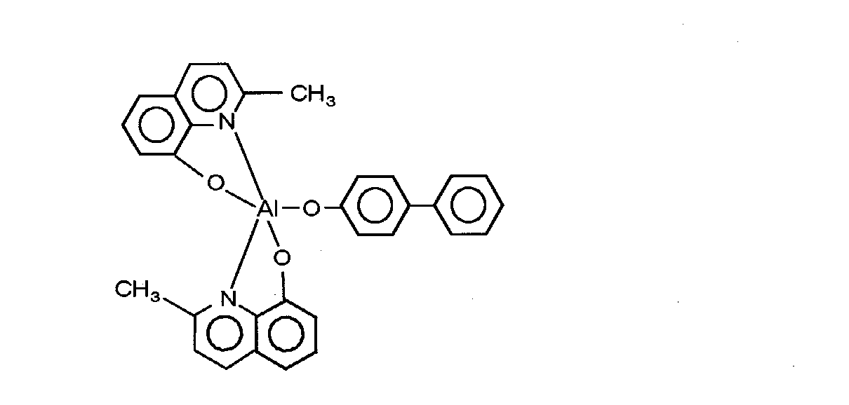
、ポリビニルカルバゾール及びこれらの化合物の誘導体など、正孔注入能を有するものであれば同様に用いることができるし、これらの化合物の積層構造としてもよい。第2の化合物として赤の波長変換物質にはペリレン、緑への波長変換物質としてクマリン6を用いたが、DCM1
【0031】
【化5】
、キナクリドン誘導体、ルブレン、DCJT
【0033】
【化6】
、ナイルレッドなどを第2の化合物として用いることができる。
【0035】
第1の化合物としてはDPVBi
【0036】
【化7】
を用いたが、1,1,4,4−テトラフェニルブタジエン、オキサジアゾール誘導体、アゾメチン亜鉛錯体、BAlq
【0038】
【化8】
、ポリビニルカルバゾール及びこれらの化合物の誘導体など、同様の効果を有する化合物であれば用いることができる。
【0040】
発光層の形成方法はここに示した方法のほか、スクリーン印刷法、スピンコート法など溶液状態で製膜する方法等、発光層中に第2の化合物が拡散する方法を用いることができる。
【0041】
陽極の形成にあたっては、TFT素子のようなアクティブ素子を形成しておいても同様の効果を発揮できる上に大容量表示することが可能となる。
【0042】
陰極の形成においては、Mg:Agの他に、仕事関数の小さな材料を用いることができ、マグネシウム、アルミニウム、リチウム、カルシウムなどのアルカリ族やアルカリ土類金属等、およびこれらの金属を用いた合金を用いることができる。
【0043】
(実施例2)
本実施例では、実施例1の構成において発光層と正孔注入輸送層との間において第2の化合物の濃度勾配が無い例を示す。
【0044】
図2に本実施例の電界発光素子の簡単な断面図を示す。
【0045】
まず清浄なガラス基板に透明電極としてITOをEB蒸着し、次にこの電極をパターニングし、さらに図2に示すように感光性ポリイミドを用いてバンクを形成した。次にこの基板の表面を波長174nmの紫外線で処理した後、この電極表面に正孔注入物質と第2の化合物の混合溶液をインクジェットヘッドで吐出して乾燥し、膜厚50nmとした。こうして作成した正孔注入層兼波長変換層上に発光層の第1の化合物を真空蒸着法により50nmの膜厚になるように蒸着した。
【0046】
次に陰極としてMg:Ag(10:1)合金をEB蒸着し、さらにエポキシ樹脂でモールドした。
【0047】
(実施例3)
本実施例では、前記発光層が、蛍光性の第1の化合物および前記第1の化合物の発する蛍光を吸収して前記蛍光よりも長波長の蛍光を発する第2の化合物の混合物から成り、しかも前記発光層中の第1の化合物に対する第2の化合物の濃度が前記発光層の厚み方向で勾配を有する電界発光素子の例を示す。
【0048】
図3は本実施例の構成を示す簡単な断面図である。
【0049】
まず清浄なガラス基板に透明電極としてITOをEB蒸着し、次にこの電極をパターニングし、さらに図3に示すように感光性ポリイミドを用いてバンクを形成した。次にこの基板の表面を波長174nmの紫外線で処理した後、この電極表面に第2の化合物を溶液状態でインクジェット法にてバンク内に製膜し、乾燥した。次に第1の化合物を、第2の化合物と相溶性の有る溶媒を用いて溶液状態にてインクジェットヘッドで吐出して乾燥し、膜厚50nmとした。
【0050】
次に陰極としてMg:Ag(10:1)合金をEB蒸着し、さらに脱気したエポキシ樹脂で不活性ガス中でモールドした。
【0051】
第1の化合物と第2の化合物の混合比(等しい濃度では膜厚に比例)は99.9:0.1から90:10の間が望ましい。この範囲から外れると発光効率が著しく低下する。
【0052】
第2の化合物として赤の波長変換物質にはペリレン、緑への波長変換物質としてクマリン6を用いたが、DCM1、キナクリドン、ルブレン、DCJT、ナイルレッド及びこれらの化合物の誘導体などを第2の化合物として用いることができる。第1の化合物としてはポリビニルカルバゾールを用いたが、DPVBi、1,1,4,4,−テトラフェニルブタジエン、オキサジアゾール、アゾメチン亜鉛錯体、BAlq及びこれらの化合物の誘導体など、同様の効果を有する化合物であれば用いることができる。
【0053】
第1の化合物は、インクジェット法による製膜のほか、印刷法を用いることもできる。
【0054】
陽極の形成にあたっては、TFT素子のようなアクティブ素子を形成しておいても同様の効果を発揮できる上に大容量表示することが可能となる。
【0055】
陰極の形成においては、Mg:Agの他に、仕事関数の小さな材料を用いることができ、マグネシウム、アルミニウム、リチウム、カルシウムなどのアルカリ族やアルカリ土類金属等、およびこれらの金属を含む合金を用いることができる。
【0056】
(実施例4)
本実施例では、実施例3において正孔注入輸送層を形成した例を示した。図4は本実施例の構成を示す簡単な断面図である。
【0057】
まず清浄なガラス基板に透明電極としてITOをEB蒸着し、次にこの電極をパターニングし、さらに図4に示すように感光性ポリイミドを用いてバンクを形成した。次にこの基板の表面を波長174nmの紫外線で処理した後、この電極表面に正孔注入輸送層としてNPDを50nmの膜厚に蒸着した。その後実施例3と同様の方法により第2の化合物および第1の化合物を製膜した。
【0058】
次に陰極としてMg:Ag(10:1)合金をEB蒸着し、さらにエポキシ樹脂でモールドした。
【0059】
(実施例5)
本実施例では、発光層を電極または電極群で挟持した電界発光素子の製造方法において、透明基板上に透明な陽極または陽極群を形成し、さらに正孔注入層を形成してもよく、次に前記第1の化合物を全面に製膜し、次に前記陽極または陽極群上に前記第2の化合物を適宜溶液としてインクジェットヘッドにより吐出し、第1の化合物層に第2の化合物を含浸させて前記発光層を形成し、その上に陰極または陰極群を形成する例を示す。
【0060】
図5は本実施例の構成を示す簡単な断面図である。
【0061】
まず清浄なガラス基板に透明電極としてITOをEB蒸着し、次にこの電極をパターニングし、さらに図5に示すように感光性ポリイミドを用いてバンクを形成した。次にこの基板の表面を波長174nmの紫外線で処理した後、この電極表面に正孔注入輸送層として銅フタロシアニンとエポキシプロピルトリエトキシシランを1:1で混合したものを塗布して200℃で焼成し、厚み50nmとし、次に発光層として第1の化合物を溶液状態にて印刷して乾燥し、膜厚40nmとした。次に
第2の化合物を溶液状態でインクジェット法にてバンク内に製膜し、乾燥した。
【0062】
次に陰極としてMg:Ag(10:1)合金をEB蒸着し、さらに脱気したエポキシ樹脂で不活性ガス中でモールドした。
【0063】
第1の化合物と第2の化合物の混合比(等しい濃度では膜厚に比例)は99.9:0.1から90:10の間が望ましい。この範囲から外れると発光効率が著しく低下する。
【0064】
第2の化合物として赤の波長変換物質にはペリレン、緑への波長変換物質としてクマリン6を用いたが、DCM1、キナクリドン、ルブレン、DCJT、ナイルレッド及びこれらの化合物の誘導体などを第2の化合物として用いることができる。
【0065】
第1の化合物としてはポリビニルカルバゾールを用いたが、DPVBi、1,1,4,4,−テトラフェニルブタジエン、オキサジアゾール、アゾメチン亜鉛錯体、BAlq及びこれらの化合物の誘導体など、同様の効果を有する化合物であれば用いることができる。
【0066】
陽極の形成にあたっては、TFT素子のようなアクティブ素子を形成しておいても同様の効果を発揮できる上に大容量表示することが可能となる。
【0067】
陰極の形成においては、Mg:Agの他に、仕事関数の小さな材料を用いることができ、マグネシウム、アルミニウム、リチウム、カルシウムなどのアルカリ族やアルカリ土類金属等、およびこれらの金属を含む合金を用いることができる。
【0068】
(実施例6)
本実施例では、発光層を対向する電極または電極群で挟持した電界発光素子の製造方法において、透明基板上に透明な陽極または陽極群を形成し、さらに正孔注入層を形成してもよく、次にこの陽極または陽極群上に前記第1の化合物と前記第2の化合物を混合して、適宜溶液としてインクジェットヘッドにより吐出して前記発光層を形成し、その上に陰極または陰極群を形成する例を示した。
【0069】
図6は本実施例の構成を示す簡単な断面図である。
【0070】
まず清浄なガラス基板に透明電極としてITOをEB蒸着し、次にこの電極をパターニングし、さらに図6に示すように感光性ポリイミドを用いてバンクを形成した。次にこの基板の表面を波長174nmの紫外線で処理した後、この電極表面に正孔注入輸送層として銅フタロシアニンとエポキシプロピルトリエトキシシランを1:1で混合したものを塗布して200℃で焼成し、厚み50nmとし、次に発光層として第1の化合物を溶液状態にて印刷して乾燥し、膜厚40nmとした。次に
第1の化合物と第2の化合物の99:1混合物を溶液状態でインクジェット法にてバンク内に製膜し、乾燥した。
【0071】
次に陰極としてMg:Ag(10:1)合金をEB蒸着し、さらに脱気したエポキシ樹脂で不活性ガス中でモールドした。
【0072】
第1の化合物と第2の化合物の混合比(等しい濃度では膜厚に比例)は99.9:0.1から90:10の間が望ましい。この範囲から外れると発光効率が著しく低下する。
【0073】
第2の化合物として赤の波長変換物質にはペリレン、緑への波長変換物質としてクマリン6を用いたが、DCM1、キナクリドン、ルブレン、DCJT、ナイルレッドおよびこれらの化合物の誘導体などを第2の化合物として用いることができる。
【0074】
第1の化合物としてはポリビニルカルバゾールを用いたが、DPVBi、1,1,4,4−テトラフェニルブタジエン、オキサジアゾール、アゾメチン亜鉛錯体、BAlq及びこれらの化合物の誘導体など、同様の効果を有する化合物であれば用いることができる。
【0075】
陽極の形成にあたっては、TFT素子のようなアクティブ素子を形成しておいても同様の効果を発揮できる上に大容量表示することが可能となる。
【0076】
陰極の形成においては、Mg:Agの他に、仕事関数の小さな材料を用いることができ、マグネシウム、アルミニウム、リチウム、カルシウムなどのアルカリ族やアルカリ土類金属等、およびこれらの金属を含む合金を用いることができる。
【0077】
(実施例7)
本実施例では、透明基板、透明な陽極または陽極群、第2の化合物と正孔注入輸送能を有する化合物からなる正孔注入輸送層、第1の化合物からなる発光層、さらに陰極または陰極群からなり、かつ正孔注入輸送層と発光層の間で、第2の化合物が濃度勾配を有する電界発光素子の例を示す。
【0078】
図1に本実施例の電界発光素子の簡単な断面図を示す。本実施例の電界発光素子の製造方法は実施例1に示した。
【0079】
こうして作製した電界発光素子は、第2の化合物の蛍光に対応した発光色を有し、第2の化合物としてクマリン6を用いた場合で発光効率は1.2lm/W、最高輝度13,000cd/m2であり、以下に示す蒸着法による場合と同等の効率となった。
【0080】
陽極の形成にあたっては、TFT素子のようなアクティブ素子を形成しておいても同様の効果を発揮できる上に大容量表示することが可能となる。
【0081】
本実施例において、発光層と陰極の間に電子注入輸送層を形成してもよく、アルミニウムキノリニウム錯体などの金属有機錯体、オキサジアゾール錯体などを用いることができる。
【0082】
陽極の形成にあたっては、TFT素子のようなアクティブ素子を形成しておいても同様の効果を発揮できる上に大容量表示することが可能となる。
【0083】
(実施例8)
本実施例では、実施例7の構成において発光層と正孔注入輸送層との間において第2の化合物の濃度勾配が無い電界発光素子の例を示す。
【0084】
図2に本実施例の電界発光素子の簡単な断面図を示す。本実施例の電界発光素子の製造方法は実施例2に示した。
【0085】
こうして作製した電界発光素子は、第2の化合物の蛍光に対応した発光色を有し、第2の化合物としてクマリン6を用いた場合で発光効率は1.2lm/W、最高輝度13,000cd/m2であり、実施例1に示した発光層を印刷法で形成する場合とほぼ同等の明るさとなった。
【0086】
本実施例において、発光層と陰極の間に電子注入輸送層を形成してもよく、アルミニウムキノリニウム錯体などの金属有機錯体、オキサジアゾール錯体などを用いることができる。
【0087】
陽極の形成にあたっては、TFT素子のようなアクティブ素子を形成しておいても同様の効果を発揮できる上に大容量表示することが可能となる。
【0088】
(実施例9)
本実施例では、透明基板、透明電極または電極群、発光層、陰極または陰極群からなる電界発光素子で、前記発光層が、第1の化合物および第2の化合物の混合物から成り、しかも前記発光層中の第1の化合物に対する第2の化合物の濃度が前記発光層の厚み方向で勾配を有する電界発光素子の例を示す。
【0089】
図3は本実施例の構成を示す簡単な断面図である。本実施例の電界発光素子の製造方法は実施例3に示した。
【0090】
こうして作製した電界発光素子は、第2の化合物の蛍光に対応した発光色を有し、第2の化合物としてクマリン6を用いた場合で発光効率は0.1lm/W、最高輝度150cd/m2であった。
【0091】
本実施例において、発光層と陰極の間に電子注入輸送層を形成してもよく、アルミニウムキノリニウム錯体などの金属有機錯体、オキサジアゾール錯体などを用いることができる。
【0092】
陽極の形成にあたっては、TFT素子のようなアクティブ素子を形成しておいても同様の効果を発揮できる上に大容量表示することが可能となる。
【0093】
(実施例10)
本実施例では、実施例9において正孔注入輸送層を形成した例を示した。
【0094】
図4は本実施例の構成を示す簡単な断面図である。実施例4に製造方法を示した。
【0095】
こうして作製した電界発光素子は、第2の化合物の蛍光に対応した発光色を有し、第2の化合物としてクマリン6を用いた場合で発光効率は0.4lm/W、最高輝度300cd/m2であった。
【0096】
本実施例において、発光層と陰極の間に電子注入輸送層を形成してもよく、アルミニウムキノリニウム錯体などの金属有機錯体、オキサジアゾール錯体などを用いることができる。
【0097】
陽極の形成にあたっては、TFT素子のようなアクティブ素子を形成しておいても同様の効果を発揮できる上に大容量表示することが可能となる。
【0098】
(実施例11)
本実施例では、透明基板、透明な陽極または陽極群、(正孔注入輸送層)、第1の化合物層、第2の化合物層、さらに陰極または陰極群からなり、かつ第1の化合物層および第2の化合物層の間に第2の化合物の濃度勾配を有する電界発光素子の例を示した。
【0099】
図5は本実施例の構成を示す簡単な断面図である。実施例5に製造方法を示した。
【0100】
こうして作製した電界発光素子は、第2の化合物の蛍光に対応した発光色を有し、第2の化合物としてクマリン6を用いた場合で発光効率は0.2lm/W、最高輝度200cd/m2であった。
【0101】
本実施例において、発光層と陰極の間に電子注入輸送層を形成してもよく、アルミニウムキノリニウム錯体などの金属有機錯体、オキサジアゾール錯体などを用いることができる。
【0102】
陽極の形成にあたっては、TFT素子のようなアクティブ素子を形成しておいても同様の効果を発揮できる上に大容量表示することが可能となる。
【0103】
(実施例12)
本実施例では、透明基板、透明な陽極または陽極群、(正孔注入輸送層)、第1の化合物と前記第2の化合物の混合層、さらに陰極または陰極群からなる電界発光素子の例を示した。
【0104】
図6は本実施例の構成を示す簡単な断面図である。実施例6に本実施例の電界発光素子の製造方法を示した。
【0105】
こうして作製した電界発光素子は、第2の化合物の蛍光に対応した発光色を有し、第2の化合物としてクマリン6を用いた場合で発光効率は0.08lm/W、最高輝度150cd/m2であった。
【0106】
本実施例において、発光層と陰極の間に電子注入輸送層を形成してもよく、アルミニウムキノリニウム錯体などの金属有機錯体、オキサジアゾール錯体などを用いることができる。
【0107】
陽極の形成にあたっては、TFT素子のようなアクティブ素子を形成しておいても同様の効果を発揮できる上に大容量表示することが可能となる。
【0108】
(実施例13)
本実施例では、発光層を対向する電極または電極群で挟持した電界発光素子の製造方法において、透明基板上に透明な陽極または陽極群を形成し、さらに正孔注入層を形成してもよく、次にこの陽極または陽極群上に第1の化合物を適宜溶液としてインクジェットヘッドにより吐出して前記発光層を形成し、その上に陰極または陰極群を形成する例を示した。
【0109】
図7は本実施例の構成を示す簡単な断面図である。
【0110】
まず清浄なガラス基板に透明電極としてITOをEB蒸着し、次にこの電極をパターニングし、さらに図7に示すように感光性ポリイミドを用いてバンクを形成した。次にこの基板の表面を波長174nmの紫外線で処理した後、この電極表面に正孔注入輸送層として銅フタロシアニンとエポキシプロピルトリエトキシシランを1:1で混合したものを塗布して200℃で焼成し、厚み50nmとし、次に発光層として第1の化合物を溶液状態にて印刷して乾燥し、膜厚40nmとした。次に
第1の化合物を溶液状態でインクジェット法にてバンク内に製膜し、乾燥した。
【0111】
次に陰極としてMg:Ag(10:1)合金をマスク越しにEB蒸着し、さらに脱気したエポキシ樹脂で不活性ガス中でモールドした。
【0112】
第1の化合物としては青色発光画素にはポリビニルカルバゾールを用いたが、DPVBi、1,1,4,4−テトラフェニルブタジエン、オキサジアゾール、アゾメチン亜鉛錯体、BAlq及びこれらの化合物の誘導体などを用いることができる。また緑色発光画素には、Alq3
【0113】
【化9】
や、青〜緑色発光物質にクマリン6などのドーパントを混合したものを用いることができる。また赤色発光画素には、ポリ(2−メトキシ−5−(2‘−エチル−ヘキシロキシ)−1,4−フェニレンビニレン)や、青〜緑色発光物質にDCM1やナイルレッドなどのドーパントを混合したものを用いることができる。
【0115】
陽極の形成にあたっては、TFT素子のようなアクティブ素子を形成しておいても同様の効果を発揮できる上に大容量表示することが可能となる。
【0116】
陰極の形成においては、Mg:Agの他に、仕事関数の小さな材料を用いることができ、マグネシウム、アルミニウム、リチウム、カルシウムなどのアルカリ族やアルカリ土類金属等、及びこれらの金属を含む合金を用いることができる。
【0117】
(実施例14)
本実施例では、実施例1から実施例13で作成した電界発光素子において電界発光素子の表面にノングレア処理そして/または減反射処理を施した例を示す。
【0118】
実施例に示した電界発光素子の透明基板上に日東電工(株)製ノングレアシートAG20を貼り付けたところ、映り込みがぼかされて視認性が向上した。またこのノングレアシートに減反射コートを施して同様に用いたところ、映り込みがほとんど気にならなくなりさらに視認性が向上した。
【0119】
ノングレアシートとしては同様の効果を有するものであれば同様に用いることができる。また減反射コートとしては屈折率の異なる層の多層コーティングや、低屈折率物質、例えばサイトップ(旭硝子社製)など弗化物高分子のコーティング等を用いることができる。
【0120】
(実施例15)
本実施例では本発明の電界発光素子を単純マトリックス駆動する実施例を示す。図8に電界発光素子と駆動回路の簡単な接続図を示した。電界発光素子を製造する際に、陽極及び陰極を短冊状の陽極群(100本)および陰極群(320本)とし、図8に示したように接続した。陽極及び陰極に印加する駆動波形は図9に示した。この駆動波形において、選択した画素には発光するに十分な電圧Vsで、かつ表示する階調に合わせたパルス幅の波形を印加している。選択しない画素には発光しきい電圧以下の電圧Vnが印加される。図9においてTfは1走査時間を示す。ここでは1/100デューティで駆動した。実施例7の電界発光素子を用いたところ、第2の化合物としてクマリン6を用いた場合で駆動電圧20Vで100cd/m2の明るさであった。
【0121】
【発明の効果】
以上本発明によれば、発光層と蛍光変換物質を組み合わせた電界発光素子において、非常に簡単な構成により、明るくコントラストの高い電界発光素子を実現できる。また非常に簡単なプロセスにより、安価に高性能な電界発光素子を製造できるようになった。このため低価格の携帯型端末、車載用等のディスプレイに応用できる。
【図面の簡単な説明】
【図1】本発明の実施例1および実施例7における電界発光素子の簡単な断面図。
【図2】本発明の実施例2および実施例8における電界発光素子の簡単な断面図。
【図3】本発明の実施例3および実施例9における電界発光素子の簡単な断面図。
【図4】本発明の実施例4および実施例10における電界発光素子の簡単な断面図。
【図5】本発明の実施例5および実施例11における電界発光素子の簡単な断面図。
【図6】本発明の実施例6および実施例12における電界発光素子の簡単な断面図。
【図7】本発明の実施例13における電界発光素子の簡単な断面図。
【図8】本発明の実施例15における電界発光素子の駆動回路周辺図。
【図9】本発明の実施例15における電界発光素子を駆動する際に用いる駆動波形図。
【符号の説明】
1…陰極、2…発光層、3…濃度勾配層、4…バンク、5…正孔注入輸送+蛍光変換層、6…陽極、7…透明基板、8…蛍光変換層、9…正孔注入輸送層、10…蛍光物質含浸発光層、11…蛍光物質混合発光層、12…電界発光素子、13…走査電極ドライバー、14…信号電極ドライバー、15…コントローラ。[0001]
BACKGROUND OF THE INVENTION
The present invention relates to a structure of an electroluminescent element using a light-emitting thin film that can be used for, for example, a laptop computer, a television, a display for mobile communication, and the like, and a manufacturing method thereof.
[0002]
[Prior art]
A light-emitting element using electroluminescence of an organic compound has high visibility due to self-emission, and is excellent in impact resistance because it is a completely solid element, and has characteristics such as a low driving voltage. The use as a light emitting element has attracted attention.
[0003]
In order to broaden the use of the organic EL element as a display element, it is obvious that multi-coloring is necessary as seen in examples of a cathode ray tube (CRT) and a liquid crystal display (LCD).
[0004]
Conventionally, as a method of manufacturing a multicolor display device using EL elements, for example, (1) a method of arranging EL materials that emit light in three primary colors of red (R), green (G), and blue (B) in a matrix form (Japanese Patent Laid-Open No. 57-157487, Japanese Patent Laid-Open No. 58-147899, Japanese Patent Laid-Open No. 3-214593, etc.), (2) A method of taking out three primary colors of RGB by combining an EL element that emits white light and a color filter ( (3) A method of converting an EL element emitting blue light and a fluorescence conversion film into three primary colors of RGB (Japanese Patent Laid-Open No. 1-315988, JP-A-2-27396, JP-A-3-194895, etc.) JP-A-3-152897) is known.
[0005]
However, the method (1) is technically difficult and cannot be manufactured at low cost because three kinds of light emitting materials must be arranged in a matrix with high definition. Since the lifetimes are often different in general, there is a drawback that the chromaticity shifts with time. Further, the method (2) has a drawback that the use efficiency of EL light, that is, the conversion efficiency is low because a part of the output light of the EL element emitting white light is extracted by a color filter. For example, if the white EL light is simply composed of RGB three primary colors having the same intensity, and the red color is taken out using the color filter, only a conversion efficiency of 33% at the maximum can be obtained. Actually, considering the emission spectrum and the visibility, only a conversion efficiency much lower than this can be obtained. On the other hand, in the method (3), if the three primary colors of RGB are obtained with a conversion efficiency of 33% or more, respectively, the method is superior to the method (2).
[0006]
By the way, a method of changing the color tone of EL emission color in various ways by arranging a fluorescent conversion film on the EL element in the stacking direction is known (Japanese Patent Publication No. 63-18319, Japanese Patent Laid-Open No. 3-152897). Of RGB, blue is emitted by the organic EL element itself, and may be used. In this case, if the conversion efficiency is strongly described, it becomes 100%. Further, green is obtained with a conversion efficiency of 80% using coumarin 153 as disclosed in Japanese Patent Laid-Open No. 3-152897. A method for converting blue light of an EL element into red with a conversion efficiency of 33% or more is disclosed in Japanese Patent Laid-Open No. 8-28633.
[0007]
[Problems to be solved by the invention]
Now, the fluorescence conversion method is excellent for the method of performing full color display in this way, but when it becomes an actual manufacturing method, the process similar to the color filter used in the conventional color liquid crystal display device is used for the manufacture of the fluorescence conversion film. It was necessary and had the problem of becoming very expensive.
[0008]
The present invention overcomes such drawbacks of the prior art and provides an electroluminescent device capable of converting the light emission color of a blue light emitting organic EL device to another color with a high conversion efficiency of 33% or more, and an inkjet method. It is an object of the present invention to provide a manufacturing method that can be used to manufacture a color electroluminescent element at low cost.
[0009]
[Means for Solving the Problems]
The electroluminescent device of the present invention includes an anode, a cathode, a light emitting layer sandwiched between the anode and the cathode and made of a fluorescent first compound, and a positive electrode disposed between the anode and the light emitting layer. A hole injecting and transporting layer, and the hole injecting and transporting layer has a charge injecting and transporting capability with the second compound that absorbs the fluorescence emitted by the first compound and emits fluorescence having a longer wavelength than the fluorescence. It consists of a mixture of compounds. According to this, since the second compound layer is disposed on the outgoing light side, all light emitted from the light emitting layer formed by the first compound is incident on the second compound layer and absorbed by the second compound. Thus, since the light is emitted after wavelength conversion, the color purity is increased. At this time, if the concentration of the second compound has a gradient between the light emitting layer and the hole injecting and transporting layer, the movement of holes is facilitated and the light emission efficiency is improved.
[0010]
In the electroluminescent device of the present invention, in the display device in which the light emitting layer is sandwiched between opposing electrodes or electrode groups, the light emitting layer absorbs the fluorescence emitted from the first fluorescent compound and the first compound. It consists of a mixture of second compounds that emit fluorescence having a wavelength longer than that of the fluorescence, and the concentration of the second compound with respect to the first compound in the light emitting layer has a gradient in the thickness direction of the light emitting layer. And the ratio of the first compound to the second compound is 99.9: 0.1 to 90:10. With this configuration, the charge injected from the electrode efficiently reaches the light emitting layer, so that the light emitting layer mainly composed of the first compound emits fluorescence of the first compound, and then this fluorescence directly or The second compound efficiently absorbs the fluorescence reflected by the cathode, and the second compound emits the fluorescence. At this time, since there is no clear interface between the first compound and the second compound, in addition to the energy transfer involving light, direct energy transfer occurs simultaneously, and the conversion efficiency is improved.
[0011]
In the electroluminescent device, a charge injecting and transporting layer is formed between the light emitting layer and the electrode. According to this configuration, charge injection is further efficiently generated in the above configuration, and as a result, the light emission efficiency is also improved.
[0012]
The first or second compound used in the above electroluminescent device is an organic compound or an organometallic compound. As a result, the drive voltage can be dramatically reduced.
[0013]
The surface of the electroluminescent element is subjected to non-glare treatment and / or anti-reflection treatment. Thereby, since the reflected light of the display surface of an electroluminescent element can be reduced or scattered, a display becomes cheap.
[0014]
In the method of manufacturing an electroluminescent element in which a light emitting layer made of a first compound is sandwiched between opposing electrodes or electrode groups, a step of forming a transparent anode or anode group on a transparent substrate; Further, a mixture of a second compound that absorbs fluorescence emitted from the first compound and emits fluorescence having a longer wavelength than the fluorescence and a compound having charge injection and transport ability is appropriately discharged as a solution by an inkjet head. Forming the hole injecting and transporting layer; and forming the first compound on the entire surface using a solvent whose compatibility with the second compound is controlled, thereby forming the first injecting and transporting layer on the hole injecting and transporting layer. And a step of forming a light emitting layer by impregnating one compound and a step of forming a cathode or a group of cathodes on the light emitting layer. According to this method, since the hole injecting and transporting layer can be patterned, a short circuit between the anodes can be avoided even when a highly conductive material having a high hole injecting property is used as the hole injecting material. At the same time, since the fluorescent conversion substance can be patterned, a full-color high-efficiency electroluminescent device can be manufactured using the best material by a simple process.
[0015]
Next, in the method for manufacturing an electroluminescent element in which the light emitting layer is sandwiched between two electrodes or electrode groups facing each other, a transparent anode or anode group is formed on a transparent substrate, and a hole injecting and transporting layer is further formed. Well, next, the first compound is formed on the entire surface, and then the second compound is appropriately discharged as a solution on the anode or the anode group by an ink jet head, and the second compound is applied to the first compound layer. The light emitting layer is impregnated to form a cathode, or an anode group is formed thereon. Alternatively, a transparent anode or anode group may be formed on a transparent substrate, and a hole injecting and transporting layer may be further formed. Next, a second compound is appropriately discharged as a solution onto the anode or anode group by an inkjet head. Further, the light emitting layer is formed by impregnating the first compound layer with the second compound by forming a film of the first compound using a solvent whose compatibility with the second compound is controlled. And a cathode or a group of cathodes is formed thereon. By these manufacturing methods, it becomes possible to easily change the emission color for each adjacent pixel, and the manufacturing cost can be reduced. When the first compound is ejected by an ink jet head, the concentration gradient in the thickness direction can be controlled by controlling the compatibility with the second compound. As a result, an electroluminescent device can be manufactured in accordance with a wide range of characteristics of the first compound and the second compound.
[0016]
Next, in the method for manufacturing an electroluminescent element in which the light emitting layer is sandwiched between two electrodes or electrode groups facing each other, a transparent anode or anode group is formed on a transparent substrate, and a hole injecting and transporting layer is further formed. Well, next, the first compound and the second compound are mixed on the anode or the anode group, and discharged as an appropriate solution onto an electrode or a charge injection / transport layer by an inkjet head to form the light emitting layer. Furthermore, a cathode or a cathode group is formed. According to this method, a full-color electroluminescent device can be manufactured at a very low cost by an extremely simple process.
[0017]
Next, in the method for manufacturing an electroluminescent element in which the light emitting layer is sandwiched between two electrodes or electrode groups facing each other, a transparent anode or anode group is formed on a transparent substrate, and a hole injecting and transporting layer is further formed. Next, the first compound is appropriately applied as a solution on the anode or the anode group by an ink jet head onto the electrode or the charge injecting and transporting layer to form the light emitting layer, and further forming the cathode or the cathode group. It is characterized by that. According to this method, a full-color electroluminescent device can be manufactured at a very low cost by an extremely simple process.
[0018]
In the electroluminescent element in the means for solving the problems described above, a bank is formed between the pixels in order to divide the pixels. Thus, mutual contamination between adjacent pixels can be prevented during film formation by the ink jet method, and diffusion of organic molecules between adjacent pixels can be prevented after element fabrication. As a result, leakage between electrodes due to the charge injection / transport layer and the light emitting layer can be prevented, and the light emission color is not mixed between the pixels, so that bright light emission can be realized.
[0019]
DETAILED DESCRIPTION OF THE INVENTION
Example 1
In this embodiment, in a method of manufacturing an electroluminescent element in which a light emitting layer is sandwiched between opposing electrodes or electrode groups, a transparent anode or anode group is formed on a transparent substrate, and then a pixel group on the anode or anode group is formed. A hole injection layer is formed by discharging a mixture of the second compound and a compound having a hole injection / transporting capability as an appropriate solution onto the ink jet head, and the first compound is mixed with the second compound. An example is shown in which a light-emitting layer is formed by impregnating a first compound layer with a second compound by forming a film on the entire surface using a solvent whose solubility is controlled, and a cathode or a cathode group is formed thereon. . FIG. 1 shows a simple cross-sectional view of the electroluminescent element of this example.
[0020]
First, ITO was EB-deposited as a transparent electrode on a clean glass substrate, this electrode was then patterned, and a bank was formed using photosensitive polyimide as shown in FIG. Next, the surface of this substrate was treated with ultraviolet rays having a wavelength of 174 nm, and then a mixed solution of a hole injection substance and a second compound was discharged onto the electrode surface with an inkjet head and dried to a film thickness of 50 nm. On the hole injection layer / wavelength conversion layer thus prepared, the first compound of the light emitting layer was printed in a solution state with a roll coater and dried to a film thickness of 50 nm.
[0021]
Next, Mg: Ag (10: 1) alloy was EB vapor-deposited as a cathode through a mask, and further molded in an inert gas with a degassed epoxy resin. Any other thermosetting resin, ultraviolet curable resin, or silicon resin containing polysilazane can be used as long as it can block air and moisture and does not attack the organic film.
[0022]
TPD as a hole injection material
[0023]
[Chemical 1]
Was used, but m-MTDATA
[0025]
[Chemical 2]
Porphine compounds such as copper phthalocyanine, NPD
[0027]
[Chemical 3]
TAD
[0029]
[Formula 4]
In addition, polyvinyl carbazole and derivatives of these compounds can be used in the same manner as long as they have hole injecting ability, and a laminated structure of these compounds may be used. Perylene was used as the red wavelength converting substance as the second compound, and Coumarin 6 was used as the wavelength converting substance into green.
[0031]
[Chemical formula 5]
, Quinacridone derivatives, rubrene, DCJT
[0033]
[Chemical 6]
Nile red or the like can be used as the second compound.
[0035]
As the first compound, DPVBi
[0036]
[Chemical 7]
1,1,4,4-tetraphenylbutadiene, oxadiazole derivative, azomethine zinc complex, BAlq
[0038]
[Chemical 8]
, Polyvinyl carbazole and derivatives of these compounds can be used as long as they have similar effects.
[0040]
As a method for forming the light emitting layer, a method in which the second compound is diffused in the light emitting layer, such as a method of forming a film in a solution state such as a screen printing method or a spin coating method, can be used.
[0041]
In forming the anode, even if an active element such as a TFT element is formed, the same effect can be exhibited and a large capacity display can be performed.
[0042]
In forming the cathode, in addition to Mg: Ag, a material having a small work function can be used, and alkali or alkaline earth metals such as magnesium, aluminum, lithium and calcium, and alloys using these metals. Can be used.
[0043]
(Example 2)
In this example, an example in which there is no concentration gradient of the second compound between the light emitting layer and the hole injecting and transporting layer in the configuration of Example 1 is shown.
[0044]
FIG. 2 shows a simple cross-sectional view of the electroluminescent element of this example.
[0045]
First, ITO was EB-deposited as a transparent electrode on a clean glass substrate, this electrode was then patterned, and a bank was formed using photosensitive polyimide as shown in FIG. Next, the surface of this substrate was treated with ultraviolet rays having a wavelength of 174 nm, and then a mixed solution of a hole injection substance and a second compound was discharged onto the electrode surface with an inkjet head and dried to a film thickness of 50 nm. On the hole injection layer / wavelength conversion layer thus prepared, the first compound of the light emitting layer was deposited by a vacuum deposition method to a thickness of 50 nm.
[0046]
Next, EB vapor deposition of Mg: Ag (10: 1) alloy was carried out as a cathode, and also it mold | molded with the epoxy resin.
[0047]
Example 3
In this embodiment, the light-emitting layer is composed of a mixture of a fluorescent first compound and a second compound that absorbs fluorescence emitted from the first compound and emits fluorescence having a longer wavelength than the fluorescence. An example of an electroluminescent element in which the concentration of the second compound with respect to the first compound in the light emitting layer has a gradient in the thickness direction of the light emitting layer is shown.
[0048]
FIG. 3 is a simple cross-sectional view showing the configuration of this embodiment.
[0049]
First, ITO was EB-deposited as a transparent electrode on a clean glass substrate, this electrode was then patterned, and a bank was formed using photosensitive polyimide as shown in FIG. Next, the surface of this substrate was treated with ultraviolet rays having a wavelength of 174 nm, and then a second compound was formed on the surface of the electrode in the form of a solution in a bank by an inkjet method and dried. Next, the 1st compound was discharged with the inkjet head in the solution state using the solvent compatible with the 2nd compound, and was dried, and it was set as 50 nm in film thickness.
[0050]
Next, Mg: Ag (10: 1) alloy was EB vapor-deposited as a cathode, and further molded with an evacuated epoxy resin in an inert gas.
[0051]
The mixing ratio of the first compound and the second compound (proportional to the film thickness at the same concentration) is preferably between 99.9: 0.1 and 90:10. If it is out of this range, the light emission efficiency is significantly reduced.
[0052]
Perylene was used as the red wavelength conversion substance as the second compound, and Coumarin 6 was used as the wavelength conversion substance into green. DCM1, quinacridone, rubrene, DCJT, Nile red, and derivatives of these compounds were used as the second compound. Can be used as Polyvinylcarbazole was used as the first compound, but it has similar effects such as DPVBi, 1,1,4,4, -tetraphenylbutadiene, oxadiazole, azomethine zinc complex, BAlq and derivatives of these compounds. Any compound can be used.
[0053]
The first compound can be formed by a printing method in addition to the film formation by the ink jet method.
[0054]
In forming the anode, even if an active element such as a TFT element is formed, the same effect can be exhibited and a large capacity display can be performed.
[0055]
In the formation of the cathode, a material having a small work function can be used in addition to Mg: Ag, and an alkali group or alkaline earth metal such as magnesium, aluminum, lithium and calcium, and an alloy containing these metals are used. Can be used.
[0056]
Example 4
In this example, the example in which the hole injection transport layer was formed in Example 3 was shown. FIG. 4 is a simple cross-sectional view showing the configuration of this embodiment.
[0057]
First, ITO was EB-deposited as a transparent electrode on a clean glass substrate, this electrode was then patterned, and a bank was formed using photosensitive polyimide as shown in FIG. Next, the surface of this substrate was treated with ultraviolet rays having a wavelength of 174 nm, and then NPD was deposited on this electrode surface as a hole injection / transport layer to a thickness of 50 nm. Thereafter, a second compound and a first compound were formed in the same manner as in Example 3.
[0058]
Next, EB vapor deposition of Mg: Ag (10: 1) alloy was carried out as a cathode, and also it mold | molded with the epoxy resin.
[0059]
(Example 5)
In this example, in the method of manufacturing an electroluminescent element in which a light emitting layer is sandwiched between electrodes or electrode groups, a transparent anode or anode group may be formed on a transparent substrate, and a hole injection layer may be further formed. The first compound is formed on the entire surface, and then the second compound is discharged as an appropriate solution onto the anode or the anode group by an ink jet head, so that the first compound layer is impregnated with the second compound. An example in which the light emitting layer is formed and a cathode or a group of cathodes is formed thereon is shown.
[0060]
FIG. 5 is a simple cross-sectional view showing the configuration of this embodiment.
[0061]
First, ITO was EB-deposited as a transparent electrode on a clean glass substrate, this electrode was then patterned, and a bank was formed using photosensitive polyimide as shown in FIG. Next, the surface of the substrate was treated with ultraviolet rays having a wavelength of 174 nm, and then a mixture of copper phthalocyanine and epoxypropyltriethoxysilane in a 1: 1 ratio was applied to the electrode surface as a hole injecting and transporting layer and baked at 200 ° C. Then, the thickness was set to 50 nm, and the first compound was printed as a light emitting layer in a solution state and dried to a thickness of 40 nm. next
The second compound was formed into a bank in the solution state by an ink jet method and dried.
[0062]
Next, Mg: Ag (10: 1) alloy was EB vapor-deposited as a cathode, and further molded with an evacuated epoxy resin in an inert gas.
[0063]
The mixing ratio of the first compound and the second compound (proportional to the film thickness at the same concentration) is preferably between 99.9: 0.1 and 90:10. If it is out of this range, the light emission efficiency is significantly reduced.
[0064]
Perylene was used as the red wavelength conversion substance as the second compound, and Coumarin 6 was used as the wavelength conversion substance into green. DCM1, quinacridone, rubrene, DCJT, Nile red, and derivatives of these compounds were used as the second compound. Can be used as
[0065]
Polyvinylcarbazole was used as the first compound, but it has similar effects such as DPVBi, 1,1,4,4, -tetraphenylbutadiene, oxadiazole, azomethine zinc complex, BAlq and derivatives of these compounds. Any compound can be used.
[0066]
In forming the anode, even if an active element such as a TFT element is formed, the same effect can be exhibited and a large capacity display can be performed.
[0067]
In the formation of the cathode, a material having a small work function can be used in addition to Mg: Ag, and an alkali group or alkaline earth metal such as magnesium, aluminum, lithium and calcium, and an alloy containing these metals are used. Can be used.
[0068]
(Example 6)
In this example, in the method of manufacturing an electroluminescent element in which the light emitting layer is sandwiched between opposing electrodes or electrode groups, a transparent anode or anode group may be formed on a transparent substrate, and a hole injection layer may be further formed. Next, the first compound and the second compound are mixed on the anode or the anode group, and the light emitting layer is formed by discharging the solution as an appropriate solution with an inkjet head, and the cathode or the cathode group is formed thereon. An example of forming was shown.
[0069]
FIG. 6 is a simple cross-sectional view showing the configuration of this embodiment.
[0070]
First, ITO was EB-deposited as a transparent electrode on a clean glass substrate, this electrode was then patterned, and a bank was formed using photosensitive polyimide as shown in FIG. Next, the surface of the substrate was treated with ultraviolet rays having a wavelength of 174 nm, and then a mixture of copper phthalocyanine and epoxypropyltriethoxysilane in a 1: 1 ratio was applied to the electrode surface as a hole injecting and transporting layer and baked at 200 ° C. Then, the thickness was set to 50 nm, and the first compound was printed as a light emitting layer in a solution state and dried to a thickness of 40 nm. next
A 99: 1 mixture of the first compound and the second compound was formed into a bank in the solution state by an inkjet method and dried.
[0071]
Next, Mg: Ag (10: 1) alloy was EB vapor-deposited as a cathode, and further molded with an evacuated epoxy resin in an inert gas.
[0072]
The mixing ratio of the first compound and the second compound (proportional to the film thickness at the same concentration) is preferably between 99.9: 0.1 and 90:10. If it is out of this range, the light emission efficiency is significantly reduced.
[0073]
Perylene was used as the red wavelength conversion substance as the second compound, and coumarin 6 was used as the wavelength conversion substance into green. Can be used as
[0074]
Polyvinylcarbazole was used as the first compound, but DPVBi, 1,1,4,4-tetraphenylbutadiene, oxadiazole, azomethine zinc complex, BAlq, and derivatives of these compounds have similar effects. Can be used.
[0075]
In forming the anode, even if an active element such as a TFT element is formed, the same effect can be exhibited and a large capacity display can be performed.
[0076]
In the formation of the cathode, a material having a small work function can be used in addition to Mg: Ag, and an alkali group or alkaline earth metal such as magnesium, aluminum, lithium and calcium, and an alloy containing these metals are used. Can be used.
[0077]
(Example 7)
In this example, a transparent substrate, a transparent anode or a group of anodes, a hole injection transport layer composed of a second compound and a compound having a hole injection transport capability, a light emitting layer composed of a first compound, and a cathode or cathode group An example of an electroluminescent element comprising the above and having a concentration gradient of the second compound between the hole injecting and transporting layer and the light emitting layer is shown.
[0078]
FIG. 1 shows a simple cross-sectional view of the electroluminescent element of this example. The manufacturing method of the electroluminescent element of this example is shown in Example 1.
[0079]
The electroluminescent device thus produced has a luminescent color corresponding to the fluorescence of the second compound, and when using coumarin 6 as the second compound, the luminous efficiency is 1.2 lm / W and the maximum luminance is 13,000 cd / m 2 The efficiency was equivalent to that obtained by the vapor deposition method shown below.
[0080]
In forming the anode, even if an active element such as a TFT element is formed, the same effect can be exhibited and a large capacity display can be performed.
[0081]
In this embodiment, an electron injecting and transporting layer may be formed between the light emitting layer and the cathode, and a metal organic complex such as an aluminum quinolinium complex, an oxadiazole complex, or the like can be used.
[0082]
In forming the anode, even if an active element such as a TFT element is formed, the same effect can be exhibited and a large capacity display can be performed.
[0083]
(Example 8)
In this example, an example of an electroluminescent element having no concentration gradient of the second compound between the light emitting layer and the hole injecting and transporting layer in the configuration of Example 7 is shown.
[0084]
FIG. 2 shows a simple cross-sectional view of the electroluminescent element of this example. The method for manufacturing the electroluminescent element of this example is shown in Example 2.
[0085]
The electroluminescent device thus produced has a luminescent color corresponding to the fluorescence of the second compound, and when using coumarin 6 as the second compound, the luminous efficiency is 1.2 lm / W and the maximum luminance is 13,000 cd / m 2 Thus, the brightness was almost the same as when the light emitting layer shown in Example 1 was formed by a printing method.
[0086]
In this embodiment, an electron injecting and transporting layer may be formed between the light emitting layer and the cathode, and a metal organic complex such as an aluminum quinolinium complex, an oxadiazole complex, or the like can be used.
[0087]
In forming the anode, even if an active element such as a TFT element is formed, the same effect can be exhibited and a large capacity display can be performed.
[0088]
Example 9
In this example, an electroluminescent device comprising a transparent substrate, a transparent electrode or electrode group, a light emitting layer, a cathode or a cathode group, the light emitting layer comprising a mixture of a first compound and a second compound, and the light emitting The example of the electroluminescent element in which the density | concentration of the 2nd compound with respect to the 1st compound in a layer has a gradient in the thickness direction of the said light emitting layer is shown.
[0089]
FIG. 3 is a simple cross-sectional view showing the configuration of this embodiment. The method for manufacturing the electroluminescent element of this example is shown in Example 3.
[0090]
The electroluminescent device thus produced has a luminescent color corresponding to the fluorescence of the second compound, and when coumarin 6 is used as the second compound, the luminous efficiency is 0.1 lm / W and the maximum luminance is 150 cd / m. 2 Met.
[0091]
In this embodiment, an electron injecting and transporting layer may be formed between the light emitting layer and the cathode, and a metal organic complex such as an aluminum quinolinium complex, an oxadiazole complex, or the like can be used.
[0092]
In forming the anode, even if an active element such as a TFT element is formed, the same effect can be exhibited and a large capacity display can be performed.
[0093]
(Example 10)
In this example, the example in which the hole injection transport layer was formed in Example 9 was shown.
[0094]
FIG. 4 is a simple cross-sectional view showing the configuration of this embodiment. Example 4 shows the production method.
[0095]
The electroluminescent device thus fabricated has a light emission color corresponding to the fluorescence of the second compound, and when using coumarin 6 as the second compound, the luminous efficiency is 0.4 lm / W and the maximum luminance is 300 cd / m. 2 Met.
[0096]
In this embodiment, an electron injecting and transporting layer may be formed between the light emitting layer and the cathode, and a metal organic complex such as an aluminum quinolinium complex, an oxadiazole complex, or the like can be used.
[0097]
In forming the anode, even if an active element such as a TFT element is formed, the same effect can be exhibited and a large capacity display can be performed.
[0098]
(Example 11)
In this example, a transparent substrate, a transparent anode or a group of anodes, (a hole injecting and transporting layer), a first compound layer, a second compound layer, and further comprising a cathode or a cathode group, and the first compound layer and An example of an electroluminescent element having a concentration gradient of the second compound between the second compound layers is shown.
[0099]
FIG. 5 is a simple cross-sectional view showing the configuration of this embodiment. Example 5 shows the production method.
[0100]
The electroluminescent device produced in this way has an emission color corresponding to the fluorescence of the second compound, and when coumarin 6 is used as the second compound, the luminous efficiency is 0.2 lm / W and the maximum luminance is 200 cd / m. 2 Met.
[0101]
In this embodiment, an electron injecting and transporting layer may be formed between the light emitting layer and the cathode, and a metal organic complex such as an aluminum quinolinium complex, an oxadiazole complex, or the like can be used.
[0102]
In forming the anode, even if an active element such as a TFT element is formed, the same effect can be exhibited and a large capacity display can be performed.
[0103]
(Example 12)
In this embodiment, an example of an electroluminescent device comprising a transparent substrate, a transparent anode or a group of anodes, a (hole injection transport layer), a mixed layer of a first compound and the second compound, and a cathode or a cathode group. Indicated.
[0104]
FIG. 6 is a simple cross-sectional view showing the configuration of this embodiment. Example 6 shows a method for manufacturing the electroluminescent element of this example.
[0105]
The electroluminescent device manufactured in this way has an emission color corresponding to the fluorescence of the second compound, and when using coumarin 6 as the second compound, the luminous efficiency is 0.08 lm / W and the maximum luminance is 150 cd / m. 2 Met.
[0106]
In this embodiment, an electron injecting and transporting layer may be formed between the light emitting layer and the cathode, and a metal organic complex such as an aluminum quinolinium complex, an oxadiazole complex, or the like can be used.
[0107]
In forming the anode, even if an active element such as a TFT element is formed, the same effect can be exhibited and a large capacity display can be performed.
[0108]
(Example 13)
In this example, in the method of manufacturing an electroluminescent element in which the light emitting layer is sandwiched between opposing electrodes or electrode groups, a transparent anode or anode group may be formed on a transparent substrate, and a hole injection layer may be further formed. Next, an example in which the light emitting layer is formed by discharging the first compound as an appropriate solution onto the anode or the anode group by an ink jet head, and the cathode or the cathode group is formed thereon is shown.
[0109]
FIG. 7 is a simple cross-sectional view showing the configuration of this embodiment.
[0110]
First, ITO was EB-deposited as a transparent electrode on a clean glass substrate, this electrode was then patterned, and a bank was formed using photosensitive polyimide as shown in FIG. Next, the surface of the substrate was treated with ultraviolet rays having a wavelength of 174 nm, and then a mixture of copper phthalocyanine and epoxypropyltriethoxysilane in a 1: 1 ratio was applied to the electrode surface as a hole injecting and transporting layer and baked at 200 ° C. Then, the thickness was set to 50 nm, and the first compound was printed as a light emitting layer in a solution state and dried to a thickness of 40 nm. next
The first compound was formed into a film in the bank by the ink jet method in a solution state and dried.
[0111]
Next, Mg: Ag (10: 1) alloy was EB vapor-deposited as a cathode through a mask, and further molded in an inert gas with a degassed epoxy resin.
[0112]
As the first compound, polyvinyl carbazole was used for the blue light emitting pixel, but DPVBi, 1,1,4,4-tetraphenylbutadiene, oxadiazole, azomethine zinc complex, BAlq, and derivatives of these compounds were used. be able to. For the green light emitting pixel, Alq3
[0113]
[Chemical 9]
Alternatively, a blue to green luminescent substance mixed with a dopant such as coumarin 6 can be used. The red light emitting pixel includes poly (2-methoxy-5- (2′-ethyl-hexyloxy) -1,4-phenylene vinylene), or a blue to green light emitting material mixed with a dopant such as DCM1 or Nile Red. Can be used.
[0115]
In forming the anode, even if an active element such as a TFT element is formed, the same effect can be exhibited and a large capacity display can be performed.
[0116]
In the formation of the cathode, a material having a small work function can be used in addition to Mg: Ag, and an alkali group or alkaline earth metal such as magnesium, aluminum, lithium and calcium, and an alloy containing these metals are used. Can be used.
[0117]
(Example 14)
In this example, an example in which non-glare treatment and / or anti-reflection treatment is performed on the surface of the electroluminescent element produced in Examples 1 to 13 will be described.
[0118]
When a non-glare sheet AG20 manufactured by Nitto Denko Corporation was pasted on the transparent substrate of the electroluminescent element shown in the examples, the reflection was blurred and the visibility was improved. When this anti-glare sheet was coated with a reduced reflection coating and used in the same way, the reflection was hardly noticed and the visibility was further improved.
[0119]
Any non-glare sheet can be used as long as it has the same effect. As the anti-reflection coating, a multilayer coating of layers having different refractive indexes, a low refractive index material, for example, a fluoride polymer coating such as CYTOP (manufactured by Asahi Glass Co., Ltd.) can be used.
[0120]
(Example 15)
In this embodiment, an embodiment in which the electroluminescent element of the present invention is driven in a simple matrix will be described. FIG. 8 shows a simple connection diagram between the electroluminescent element and the drive circuit. When manufacturing the electroluminescent device, the anode and the cathode were formed into strip-shaped anode groups (100) and cathode groups (320) and connected as shown in FIG. The drive waveforms applied to the anode and cathode are shown in FIG. In this drive waveform, a voltage having a voltage Vs sufficient for light emission and a pulse width matching the gradation to be displayed is applied to the selected pixel. A voltage Vn equal to or lower than the light emission threshold voltage is applied to the unselected pixels. In FIG. 9, Tf indicates one scanning time. Here, it was driven at 1/100 duty. When the electroluminescent element of Example 7 was used, 100 cd / m at a driving voltage of 20 V when coumarin 6 was used as the second compound. 2 Was the brightness.
[0121]
【The invention's effect】
As described above, according to the present invention, a bright and high-contrast electroluminescent element can be realized with a very simple configuration in an electroluminescent element in which a light emitting layer and a fluorescence conversion substance are combined. In addition, a high-performance electroluminescent device can be manufactured at a low cost by a very simple process. For this reason, it can be applied to low-priced portable terminals and displays for in-vehicle use.
[Brief description of the drawings]
FIG. 1 is a simple cross-sectional view of an electroluminescent element according to Example 1 and Example 7 of the present invention.
FIG. 2 is a simple cross-sectional view of electroluminescent elements according to Example 2 and Example 8 of the present invention.
FIG. 3 is a simple cross-sectional view of electroluminescent elements according to Example 3 and Example 9 of the present invention.
4 is a simple cross-sectional view of an electroluminescent element according to Example 4 and Example 10 of the present invention. FIG.
FIG. 5 is a simple cross-sectional view of electroluminescent elements according to Example 5 and Example 11 of the present invention.
6 is a simple cross-sectional view of an electroluminescent element according to Example 6 and Example 12 of the present invention. FIG.
FIG. 7 is a simple cross-sectional view of an electroluminescent element according to Example 13 of the present invention.
FIG. 8 is a peripheral view of a drive circuit for an electroluminescent element in Example 15 of the present invention.
FIG. 9 is a drive waveform diagram used when driving an electroluminescent element according to Example 15 of the present invention.
[Explanation of symbols]
DESCRIPTION OF
Claims (5)
陰極と、
前記陽極と前記陰極により挟持され、蛍光性の第1の化合物から成る発光層と、
前記陽極と前記発光層との間に配置された正孔注入輸送層とを有し、
前記正孔注入輸送層が、前記第1の化合物の発する蛍光を吸収して前記蛍光よりも長波長の蛍光を発する第2の化合物と電荷注入輸送能を有する化合物の混合物からなることを特徴とする電界発光素子。The anode,
A cathode,
A light emitting layer sandwiched between the anode and the cathode and made of a fluorescent first compound;
A hole injection transport layer disposed between the anode and the light emitting layer;
The hole injecting and transporting layer comprises a mixture of a second compound that absorbs fluorescence emitted from the first compound and emits fluorescence having a longer wavelength than the fluorescence and a compound having charge injecting and transporting capability. An electroluminescent device.
透明基板上に透明な陽極または陽極群を形成する工程と、
前記陽極または陽極群上に、前記第1の化合物の発する蛍光を吸収して前記蛍光よりも長波長の蛍光を発する第2の化合物と電荷注入輸送能を有する化合物の混合物を適宜溶液としてインクジェットヘッドにより吐出することにより正孔注入輸送層を形成する工程と、
前記第1の化合物を、前記第2の化合物との相溶性を制御した溶媒を用いて全面に製膜することにより、前記正孔注入輸送層に前記第1の化合物を含浸させて前記発光層を形成する工程と、
前記発光層の上に陰極または陰極群を形成する工程と、
を有することを特徴とする電界発光素子の製造方法。In the method for manufacturing an electroluminescent element in which a light emitting layer made of a first compound is sandwiched between opposing electrodes or electrode groups,
Forming a transparent anode or group of anodes on a transparent substrate;
An ink jet head in which a mixture of a second compound that emits fluorescence having a wavelength longer than that of the fluorescence and a compound having charge injection / transport ability is appropriately used as a solution on the anode or the anode group. Forming a hole injecting and transporting layer by discharging with,
The light emitting layer is formed by impregnating the first compound in the hole injecting and transporting layer by forming the first compound on the entire surface using a solvent whose compatibility with the second compound is controlled. Forming a step;
Forming a cathode or a group of cathodes on the light emitting layer;
A method for producing an electroluminescent element, comprising:
Priority Applications (5)
| Application Number | Priority Date | Filing Date | Title |
|---|---|---|---|
| JP23632697A JP3861400B2 (en) | 1997-09-01 | 1997-09-01 | Electroluminescent device and manufacturing method thereof |
| PCT/JP1998/003675 WO1999012396A1 (en) | 1997-09-01 | 1998-08-19 | Electroluminescent element and method of producing the same |
| US09/297,500 US6575800B1 (en) | 1997-09-01 | 1998-08-19 | Electroluminescent element and method of producing the same |
| TW087114149A TW406519B (en) | 1997-09-01 | 1998-08-26 | Electro-luminescent element and method of producing the same |
| US10/339,253 US6825611B2 (en) | 1997-09-01 | 2003-01-06 | Electroluminescent elements with light-emitting layer containing first and second compounds |
Applications Claiming Priority (1)
| Application Number | Priority Date | Filing Date | Title |
|---|---|---|---|
| JP23632697A JP3861400B2 (en) | 1997-09-01 | 1997-09-01 | Electroluminescent device and manufacturing method thereof |
Publications (2)
| Publication Number | Publication Date |
|---|---|
| JPH1174083A JPH1174083A (en) | 1999-03-16 |
| JP3861400B2 true JP3861400B2 (en) | 2006-12-20 |
Family
ID=16999156
Family Applications (1)
| Application Number | Title | Priority Date | Filing Date |
|---|---|---|---|
| JP23632697A Expired - Lifetime JP3861400B2 (en) | 1997-09-01 | 1997-09-01 | Electroluminescent device and manufacturing method thereof |
Country Status (4)
| Country | Link |
|---|---|
| US (2) | US6575800B1 (en) |
| JP (1) | JP3861400B2 (en) |
| TW (1) | TW406519B (en) |
| WO (1) | WO1999012396A1 (en) |
Cited By (1)
| Publication number | Priority date | Publication date | Assignee | Title |
|---|---|---|---|---|
| CN109671872A (en) * | 2018-12-26 | 2019-04-23 | 上海晶合光电科技有限公司 | A kind of preparation method of gradient color light-emitting organic electroluminescent device |
Families Citing this family (43)
| Publication number | Priority date | Publication date | Assignee | Title |
|---|---|---|---|---|
| US7090890B1 (en) * | 1998-04-13 | 2006-08-15 | The Trustees Of Princeton University | Modification of polymer optoelectronic properties after film formation by impurity addition or removal |
| JP3692844B2 (en) * | 1998-07-24 | 2005-09-07 | セイコーエプソン株式会社 | Electroluminescent device and electronic device |
| US6910933B1 (en) | 1999-10-05 | 2005-06-28 | Matsushita Electric Industrial Co., Ltd. | Light emitting element and producing method thereof, and display device and lighting device using the same |
| TW468283B (en) | 1999-10-12 | 2001-12-11 | Semiconductor Energy Lab | EL display device and a method of manufacturing the same |
| TW480722B (en) | 1999-10-12 | 2002-03-21 | Semiconductor Energy Lab | Manufacturing method of electro-optical device |
| WO2001039272A1 (en) * | 1999-11-29 | 2001-05-31 | Koninklijke Philips Electronics N.V. | Organic electroluminescent device and a method of manufacturing thereof |
| TW495808B (en) * | 2000-02-04 | 2002-07-21 | Semiconductor Energy Lab | Thin film formation apparatus and method of manufacturing self-light-emitting device using thin film formation apparatus |
| JP4785257B2 (en) * | 2000-02-04 | 2011-10-05 | 株式会社半導体エネルギー研究所 | Method for manufacturing light emitting device |
| US6869635B2 (en) * | 2000-02-25 | 2005-03-22 | Seiko Epson Corporation | Organic electroluminescence device and manufacturing method therefor |
| TWI226205B (en) * | 2000-03-27 | 2005-01-01 | Semiconductor Energy Lab | Self-light emitting device and method of manufacturing the same |
| JP2001341296A (en) * | 2000-03-31 | 2001-12-11 | Seiko Epson Corp | Thin film forming method by ink jet method, ink jet apparatus, method of manufacturing organic EL element, organic EL element |
| WO2001074121A1 (en) | 2000-03-31 | 2001-10-04 | Seiko Epson Corporation | Organic el device and method of manufacture thereof |
| WO2002009478A1 (en) | 2000-07-24 | 2002-01-31 | Tdk Corporation | Luminescent device |
| TW518909B (en) * | 2001-01-17 | 2003-01-21 | Semiconductor Energy Lab | Luminescent device and method of manufacturing same |
| JP2002280186A (en) * | 2001-03-19 | 2002-09-27 | Semiconductor Energy Lab Co Ltd | Light emitting device and method for producing it |
| US7301279B2 (en) | 2001-03-19 | 2007-11-27 | Semiconductor Energy Laboratory Co., Ltd. | Light-emitting apparatus and method of manufacturing the same |
| JP2003022892A (en) | 2001-07-06 | 2003-01-24 | Semiconductor Energy Lab Co Ltd | Light emitting device manufacturing method |
| KR20020025918A (en) * | 2002-02-15 | 2002-04-04 | 박병주 | Organic semiconducting devices and organic electroluminescent devices produced by using wet process |
| KR100563675B1 (en) * | 2002-04-09 | 2006-03-28 | 캐논 가부시끼가이샤 | Organic light emitting device and organic light emitting device package |
| JP3902981B2 (en) * | 2002-06-04 | 2007-04-11 | キヤノン株式会社 | Organic light emitting device and display device |
| US7098060B2 (en) * | 2002-09-06 | 2006-08-29 | E.I. Du Pont De Nemours And Company | Methods for producing full-color organic electroluminescent devices |
| US20040096570A1 (en) * | 2002-11-15 | 2004-05-20 | Michael Weaver | Structure and method of fabricating organic devices |
| US20040232385A1 (en) * | 2003-05-21 | 2004-11-25 | Kram Shari L. | Blend of viscosity modifier and luminescent compound |
| US20050100657A1 (en) * | 2003-11-10 | 2005-05-12 | Macpherson Charles D. | Organic material with a region including a guest material and organic electronic devices incorporating the same |
| US7067841B2 (en) * | 2004-04-22 | 2006-06-27 | E. I. Du Pont De Nemours And Company | Organic electronic devices |
| WO2006002668A1 (en) * | 2004-06-30 | 2006-01-12 | Fraunhofer-Gesellschaft zur Förderung der angewandten Forschung e.V. | Light-emitting diode matrix and method for producing a light-emitting diode matrix |
| US7858145B2 (en) * | 2004-08-31 | 2010-12-28 | Canon Kabushiki Kaisha | Method of manufacturing electroconductive member pattern, and methods of manufacturing electron source and image displaying apparatus each using the same |
| US20060132028A1 (en) * | 2004-12-16 | 2006-06-22 | Lexmark International, Inc. | Electroluminescent display construction using printing technology |
| US7268006B2 (en) * | 2004-12-30 | 2007-09-11 | E.I. Du Pont De Nemours And Company | Electronic device including a guest material within a layer and a process for forming the same |
| US7645177B2 (en) | 2005-05-07 | 2010-01-12 | Hewlett-Packard Development Company, L.P. | Electroluminescent panel with inkjet-printed electrode regions |
| CN101171525A (en) * | 2005-05-09 | 2008-04-30 | 皇家飞利浦电子股份有限公司 | Detuning of RF Shielded MRI Scanning Room |
| US20070096640A1 (en) * | 2005-08-19 | 2007-05-03 | Gang Yu | Methods for producing full color organic electroluminescent devices |
| US20070215883A1 (en) * | 2006-03-20 | 2007-09-20 | Dixon Michael J | Electroluminescent Devices, Subassemblies for use in Making Electroluminescent Devices, and Dielectric Materials, Conductive Inks and Substrates Related Thereto |
| JP4565573B2 (en) * | 2006-09-07 | 2010-10-20 | 株式会社フューチャービジョン | Manufacturing method of liquid crystal display panel |
| TWI323826B (en) * | 2006-11-15 | 2010-04-21 | Ether Precision Inc | The manufacturing process of the combine of optical lens and chip |
| US20080166566A1 (en) * | 2006-12-29 | 2008-07-10 | Shiva Prakash | Process for forming an organic light-emitting diode and devices made by the process |
| WO2009084413A1 (en) * | 2007-12-28 | 2009-07-09 | Konica Minolta Holdings, Inc. | Organic electroluminescent device and method for manufacturing organic electroluminescent device |
| US8288187B2 (en) | 2010-01-20 | 2012-10-16 | Universal Display Corporation | Electroluminescent devices for lighting applications |
| DE102010006280A1 (en) * | 2010-01-30 | 2011-08-04 | Merck Patent GmbH, 64293 | color conversion |
| US8796674B2 (en) | 2010-02-17 | 2014-08-05 | Konica Minolta Holdings, Inc. | Method of manufacturing organic electronic device, and organic electronic device |
| DE102010054280B4 (en) * | 2010-12-13 | 2025-05-22 | OSRAM Opto Semiconductors Gesellschaft mit beschränkter Haftung | Method for producing a luminescence conversion substance layer, composition therefor and component comprising such a luminescence conversion substance layer |
| KR20180077439A (en) | 2016-12-29 | 2018-07-09 | 엘지디스플레이 주식회사 | Electroluminescent display device and method of manufacturing the same |
| TW202110788A (en) * | 2019-05-03 | 2021-03-16 | 德商麥克專利有限公司 | Electronic device |
Family Cites Families (19)
| Publication number | Priority date | Publication date | Assignee | Title |
|---|---|---|---|---|
| JP2814435B2 (en) * | 1987-03-02 | 1998-10-22 | イーストマン・コダック・カンパニー | Electroluminescent device with improved thin film emission band |
| JPH02261889A (en) | 1989-03-31 | 1990-10-24 | Toshiba Corp | organic electroluminescent device |
| JP2773297B2 (en) | 1989-09-28 | 1998-07-09 | 日本電気株式会社 | Organic thin film EL device |
| JP3101300B2 (en) | 1990-07-13 | 2000-10-23 | 三洋電機株式会社 | Organic electroluminescent device |
| JP3114197B2 (en) | 1990-11-02 | 2000-12-04 | 日本電気株式会社 | Voice parameter coding method |
| CA2085445A1 (en) | 1991-12-30 | 1993-07-01 | Jon E. Littman | Efficient organic electroluminescent device of simplified construction |
| US5294869A (en) * | 1991-12-30 | 1994-03-15 | Eastman Kodak Company | Organic electroluminescent multicolor image display device |
| US5429884A (en) * | 1992-01-17 | 1995-07-04 | Pioneer Electronic Corporation | Organic electroluminescent element |
| JP3219450B2 (en) * | 1992-01-24 | 2001-10-15 | 旭硝子株式会社 | Method for producing conductive film, low reflection conductive film and method for producing the same |
| JPH06215874A (en) * | 1993-01-20 | 1994-08-05 | Idemitsu Kosan Co Ltd | Organic electroluminescent element |
| JP3332491B2 (en) * | 1993-08-27 | 2002-10-07 | 三洋電機株式会社 | Organic EL device |
| JP3534445B2 (en) * | 1993-09-09 | 2004-06-07 | 隆一 山本 | EL device using polythiophene |
| DE69418826T2 (en) * | 1993-11-22 | 1999-10-21 | Ciba Specialty Chemicals Holding Inc., Basel | Compositions for the production of structured color images and their use |
| JP3463362B2 (en) | 1993-12-28 | 2003-11-05 | カシオ計算機株式会社 | Method of manufacturing electroluminescent device and electroluminescent device |
| JPH08321381A (en) * | 1995-05-26 | 1996-12-03 | Chisso Corp | Organic electroluminescent device |
| JP3719743B2 (en) * | 1995-08-09 | 2005-11-24 | 株式会社日立製作所 | Plasma display panel |
| JP3229223B2 (en) * | 1995-10-13 | 2001-11-19 | キヤノン株式会社 | Method of manufacturing electron-emitting device, electron source and image forming apparatus, and metal composition for manufacturing electron-emitting device |
| US5747183A (en) * | 1996-11-04 | 1998-05-05 | Motorola, Inc. | Organic electroluminescent light emitting material and device using same |
| US5895695A (en) * | 1997-03-28 | 1999-04-20 | Rowley; William W. | Crosslinked overmolded plumbing tubes |
-
1997
- 1997-09-01 JP JP23632697A patent/JP3861400B2/en not_active Expired - Lifetime
-
1998
- 1998-08-19 US US09/297,500 patent/US6575800B1/en not_active Expired - Lifetime
- 1998-08-19 WO PCT/JP1998/003675 patent/WO1999012396A1/en not_active Ceased
- 1998-08-26 TW TW087114149A patent/TW406519B/en active
-
2003
- 2003-01-06 US US10/339,253 patent/US6825611B2/en not_active Expired - Lifetime
Cited By (2)
| Publication number | Priority date | Publication date | Assignee | Title |
|---|---|---|---|---|
| CN109671872A (en) * | 2018-12-26 | 2019-04-23 | 上海晶合光电科技有限公司 | A kind of preparation method of gradient color light-emitting organic electroluminescent device |
| CN109671872B (en) * | 2018-12-26 | 2020-12-01 | 上海晶合光电科技有限公司 | A kind of preparation method of gradient color light-emitting organic electroluminescent device |
Also Published As
| Publication number | Publication date |
|---|---|
| US6575800B1 (en) | 2003-06-10 |
| US6825611B2 (en) | 2004-11-30 |
| TW406519B (en) | 2000-09-21 |
| WO1999012396A1 (en) | 1999-03-11 |
| JPH1174083A (en) | 1999-03-16 |
| US20030141810A1 (en) | 2003-07-31 |
Similar Documents
| Publication | Publication Date | Title |
|---|---|---|
| JP3861400B2 (en) | Electroluminescent device and manufacturing method thereof | |
| EP0969701B1 (en) | Electroluminescent device | |
| KR100670543B1 (en) | Organic electroluminescent device | |
| US6023371A (en) | Color conversion material, and organic electroluminescent color display using the same | |
| US6821553B2 (en) | Method of manufacturing organic EL element, organic EL element, and organic EL display device | |
| JPWO1998034437A1 (en) | Organic electroluminescent display device | |
| JPH1187062A (en) | EL device | |
| US20030222576A1 (en) | Full color organic light-emitting display device | |
| JP3852518B2 (en) | Organic electroluminescence device | |
| JP2000091073A (en) | Organic electroluminescent device | |
| JPH11345688A (en) | Organic el display | |
| JP2000012227A (en) | Organic electroluminescent device | |
| JP3852517B2 (en) | Organic electroluminescence device | |
| JP2000012226A (en) | Organic electroluminescent device | |
| JP2000091077A (en) | Organic electroluminescent device | |
| KR20070008071A (en) | Organic EL display device having a stacked structure | |
| JP2000012225A (en) | Organic electroluminescent device | |
| KR100528911B1 (en) | Organic electro luminescence display device | |
| JP3690373B2 (en) | Organic EL display and manufacturing method thereof | |
| JP2000012228A (en) | Organic electroluminescent device | |
| JP2001093664A (en) | Manufacturing method of organic EL element | |
| JP2006269100A (en) | Display device | |
| Fukuda et al. | Organic LED full color passive‐matrix display | |
| JP2004303609A (en) | Organic el display for color display | |
| JP3693042B2 (en) | Organic multicolor light emitting display element and method for manufacturing the same |
Legal Events
| Date | Code | Title | Description |
|---|---|---|---|
| A131 | Notification of reasons for refusal |
Free format text: JAPANESE INTERMEDIATE CODE: A131 Effective date: 20060620 |
|
| A521 | Request for written amendment filed |
Free format text: JAPANESE INTERMEDIATE CODE: A523 Effective date: 20060809 |
|
| TRDD | Decision of grant or rejection written | ||
| A01 | Written decision to grant a patent or to grant a registration (utility model) |
Free format text: JAPANESE INTERMEDIATE CODE: A01 Effective date: 20060905 |
|
| A61 | First payment of annual fees (during grant procedure) |
Free format text: JAPANESE INTERMEDIATE CODE: A61 Effective date: 20060918 |
|
| R150 | Certificate of patent or registration of utility model |
Free format text: JAPANESE INTERMEDIATE CODE: R150 |
|
| FPAY | Renewal fee payment (event date is renewal date of database) |
Free format text: PAYMENT UNTIL: 20101006 Year of fee payment: 4 |
|
| FPAY | Renewal fee payment (event date is renewal date of database) |
Free format text: PAYMENT UNTIL: 20101006 Year of fee payment: 4 |
|
| FPAY | Renewal fee payment (event date is renewal date of database) |
Free format text: PAYMENT UNTIL: 20111006 Year of fee payment: 5 |
|
| FPAY | Renewal fee payment (event date is renewal date of database) |
Free format text: PAYMENT UNTIL: 20121006 Year of fee payment: 6 |
|
| FPAY | Renewal fee payment (event date is renewal date of database) |
Free format text: PAYMENT UNTIL: 20121006 Year of fee payment: 6 |
|
| FPAY | Renewal fee payment (event date is renewal date of database) |
Free format text: PAYMENT UNTIL: 20131006 Year of fee payment: 7 |
|
| S531 | Written request for registration of change of domicile |
Free format text: JAPANESE INTERMEDIATE CODE: R313531 |
|
| R350 | Written notification of registration of transfer |
Free format text: JAPANESE INTERMEDIATE CODE: R350 |
|
| EXPY | Cancellation because of completion of term |