JP3860344B2 - Optical disk reproduction signal jitter measurement apparatus, optical disk reproduction signal jitter measurement method, optical disk recording and / or reproduction apparatus, and optical disk reproduction method - Google Patents
Optical disk reproduction signal jitter measurement apparatus, optical disk reproduction signal jitter measurement method, optical disk recording and / or reproduction apparatus, and optical disk reproduction method Download PDFInfo
- Publication number
- JP3860344B2 JP3860344B2 JP25880198A JP25880198A JP3860344B2 JP 3860344 B2 JP3860344 B2 JP 3860344B2 JP 25880198 A JP25880198 A JP 25880198A JP 25880198 A JP25880198 A JP 25880198A JP 3860344 B2 JP3860344 B2 JP 3860344B2
- Authority
- JP
- Japan
- Prior art keywords
- reproduction signal
- jitter
- signal
- optical disk
- waveform
- Prior art date
- Legal status (The legal status is an assumption and is not a legal conclusion. Google has not performed a legal analysis and makes no representation as to the accuracy of the status listed.)
- Expired - Fee Related
Links
Images


Classifications
-
- G—PHYSICS
- G01—MEASURING; TESTING
- G01R—MEASURING ELECTRIC VARIABLES; MEASURING MAGNETIC VARIABLES
- G01R29/00—Arrangements for measuring or indicating electric quantities not covered by groups G01R19/00 - G01R27/00
- G01R29/26—Measuring noise figure; Measuring signal-to-noise ratio
-
- G—PHYSICS
- G11—INFORMATION STORAGE
- G11B—INFORMATION STORAGE BASED ON RELATIVE MOVEMENT BETWEEN RECORD CARRIER AND TRANSDUCER
- G11B20/00—Signal processing not specific to the method of recording or reproducing; Circuits therefor
- G11B20/10—Digital recording or reproducing
-
- G—PHYSICS
- G11—INFORMATION STORAGE
- G11B—INFORMATION STORAGE BASED ON RELATIVE MOVEMENT BETWEEN RECORD CARRIER AND TRANSDUCER
- G11B20/00—Signal processing not specific to the method of recording or reproducing; Circuits therefor
- G11B20/10—Digital recording or reproducing
- G11B20/14—Digital recording or reproducing using self-clocking codes
- G11B20/1403—Digital recording or reproducing using self-clocking codes characterised by the use of two levels
Landscapes
- Engineering & Computer Science (AREA)
- Signal Processing (AREA)
- Physics & Mathematics (AREA)
- General Physics & Mathematics (AREA)
- Optical Recording Or Reproduction (AREA)
- Testing Of Optical Devices Or Fibers (AREA)
- Signal Processing For Digital Recording And Reproducing (AREA)
Description
【0001】
【発明の属する技術分野】
本発明は、所定の変調規則に従ったデジタルデータが記録された光ディスクの再生信号のジッタ成分を計測する光ディスクの再生信号のジッタ計測装置、及び、光ディスクの再生信号のジッタ計測方法に関する。また、本発明は、光ディスクを再生する光ディスクの記録及び/又は再生装置、並びに、光ディスクの再生方法に関する。
【0002】
【従来の技術】
デジタルデータが記録された光ディスクを再生する光ディスクドライブでは、光学ピックアップにより再生(RF)信号を検出し、このRF信号を2値化してデジタルデータを生成する。具体的には、光ディスクドライブでは、図7(a)に示すようなRF信号を、所定のスライスレベルで2値化し、図7(b)に示すようなデジタルデータを生成する。
【0003】
また、一般に、光ディスクには、所定の変調方式に従って変調されたデジタルデータが記録されている。例えば、いわゆるコンパクトディスクでは、デジタルデータの1周期をTとした場合、記録される信号が、3Tから11Tの周期の信号に変調され、これらの各周期の波形がランダムに記録されている。また、例えば、デジタルビデオディスクでは、デジタルデータの1周期をTとした場合、記録される信号が、3Tから14Tの周期の信号に変調され、これらの各周期の波形がランダムに記録されている。光ディスクドライブでは、このような所定の変調方式に従ったデジタルデータを、光ディスクから信号を再生し、この信号を2値化し、デジタルデータを生成することとなる。
【0004】
ところで、このように光ディスクドライブにより2値化されたデジタルデータは、一般に、周期方向にノイズが乗ったかたちで、すなわち、ジッタ成分が含まれたかたちで、再生されてしまう。例えば、光ディスクから再生したRF信号のうち3Tの周期の波形だけ取り出してみた場合、このRF信号の波形の周期は、理論周期3Tに対してジッタ成分が含まれた3T±σ(σ:ジッタ成分)となる。
【0005】
このように2値化したデジタルデータにジッタ成分が含まれて再生される理由としては、例えば、光ディスクの記録信号に含まれるノイズの影響や、光ディスクに記録された信号を検出する光学ピックアップの特性の影響などがある。
【0006】
ここで、従来より、このような光ディスクから再生したデジタルデータのジッタ成分を検出するジッタ計測装置が知られている。このジッタ計測装置は、光ディスクから再生したRF信号のジッタ成分を計測して、光ディスクの特性や光学ピックアップの特性を知るために用いられる。
【0007】
以下、従来より光ディスクの再生信号のジッタ成分の計測に用いられていた第1から第3のジッタ計測装置について説明する。
【0008】
従来よりジッタ計測に用いられていた第1のジッタ計測装置は、積分回路によりデジタルデータの時間幅を電圧値として求め、ジッタ成分を計測するものである。
【0009】
まず、この第1のジッタ計測装置では、図8に示すように、RF信号を所定のスライスレベルで2値化し、デジタルデータを生成する。そして、この第1のジッタ計測装置では、RF信号がスライスレベルとなる時点で、すなわち、デジタルデータの立ち上がりエッジで、積分回路を動作させる。続いて、この第1のジッタ計測装置では、RF信号が次のスライスレベルとなる時点で、すなわち、デジタルデータの立ち下がりエッジで、積分回路を停止させる。この第1のジッタ計測装置は、このときの積分回路の出力電圧を、デジタルデータの時間幅として計測する。
【0010】
従って、この第1のジッタ計測装置では、この積分回路の出力電圧を、所定周期に対応する電圧値と比較することにより、電圧値に変換されたジッタ値(σV)を検出することができる。
【0011】
なお、この第1のジッタ計測装置では、時定数に応じて積分回路の特性が定まるので、1つの積分回路により、変調され光ディスクに記録されている複数の周期の波形の内、1の周期の波形に対応するジッタ成分のみの測定しかできない。つまり、この第1のジッタ計測装置では、再生する光ディスクがコンパクトディスクであれば、1つの積分回路により、3Tの周期の波形のジッタ成分のみを測定し、他の周期の波形例えば4Tから11Tの波形のジッタ成分の測定はできない。
【0012】
つぎに、従来ジッタ計測に用いられていた第2のジッタ計測装置は、いわゆるタイムインターバルアナライザといわれる装置を用いたもので、デジタルデータの時間幅を高速クロックでカウントし、このカウント出力でジッタ成分を検出するものである。
【0013】
まず、この第2のジッタ計測装置では、図9に示すように、RF信号を所定のスライスレベルで2値化し、デジタルデータを生成する。そして、この第2のジッタ計測装置では、RF信号がスライスレベルとなる時点で、すなわち、デジタルデータの立ち上がりエッジで、クロック回路を動作させるとともに、このクロック回路が出力するクロック数のカウントを開始する。続いて、この第2のジッタ計測装置では、RF信号が次のスライスレベルとなる時点で、すなわち、デジタルデータの立ち下がりエッジで、クロック回路を停止させる。この第2のジッタ計測装置では、このときのカウント数が、デジタルデータの時間幅となる。
【0014】
従って、この第2のジッタ計測装置では、このカウンタのカウント数を、所定周期におけるカウント数と比較することにより、ジッタ値を検出することができる。
【0015】
つぎに、従来ジッタ計測に用いられていた第3のジッタ計測装置は、上記第1のジッタ計測装置と上記第2のジッタ計測装置を応用したものである。
【0016】
まず、この第3のジッタ計測装置では、図10に示すように、RF信号を所定のスライスレベルで2値化し、デジタルデータを生成する。このとき、この第3のジッタ計測装置では、クロック回路が所定のクロック周波数で、クロックを発生し続けている。この第3のジッタ計測装置では、RF信号がスライスレベルとなる時点で、すなわち、デジタルデータの立ち上がりエッジで、クロック回路を動作させるとともに、このクロック回路が出力するクロック数をカウンタによりカウントする。また、この第3のジッタ計測装置では、このデジタルデータの立ち上がりエッジで、積分回路の動作を開始する。続いて、この第3のジッタ計測装置では、デジタルデータの立ち上がりエッジの直後に発生されたクロックのタイミングで、積分回路の動作を停止する。そして、この第3のジッタ計測装置では、このときの積分回路の出力電圧V1を計測し、この出力電圧V1を時間幅に変換して、デジタルデータの第1の時間幅t1とする。
【0017】
また、この第3のジッタ計測装置では、RF信号が次のスライスレベルとなる時点の直前のクロックのタイミング、すなわち、デジタルデータの立ち下がりエッジの直前のクロックのタイミングで再度積分回路を動作させる。そして、この第3のジッタ計測装置では、RF信号が次のスライスレベルとなる時点で、すなわち、デジタルデータの立ち下がりエッジで、積分回路を停止させる。
【0018】
そして、この第3のジッタ計測装置では、デジタルデータの立ち下がりタイミングでのカウンタのカウント数を検出し、このカウント数と上記クロック周波数に基づき、デジタルデータの立ち上がりエッジの直後のクロックのタイミングからデジタルデータの立ち下がりエッジの直前のクロックのタイミングまでの時間幅を求め、この時間幅を第2の時間幅t2とする。また、この第3のジッタ計測装置では、このときの積分回路の出力電圧V3を計測し、この出力電圧V3を時間幅に変換して、デジタルデータの第3の時間幅t3とする。
【0019】
従って、この第3のジッタ計測装置では、上記第1の時間幅t1、上記時間幅t2及び上記時間幅t3を全て加算することにより、デジタルデータの時間幅と計測することができる。そして、この第3のジッタ計測装置では、デジタルデータの時間幅と、理論値を比較することにより、ジッタ値を検出することができる。
【0020】
【発明が解決しようとする課題】
ところが、上述した従来の第1から第3のジッタ計測装置では、以下に述べる問題点があった。
【0021】
上記第1のジッタ計測装置では、積分回路を用いてアナログで時間幅を計測するため、ノイズに弱く安定して時間幅を計測することが困難であった。また、上記第1のジッタ計測装置では、1つの積分回路により1つの周期の波形のジッタ成分のみしか計測できないため、複数の周期の波形のジッタ成分を計測するには、測定する周期の波形の数だけ積分回路が必要であった。すなわち、上記第1のジッタ計測装置では、例えば、コンパクトディスクに含まれる3Tから11Tまでの周期の波形の全てのジッタ成分を検出するために、時定数が異なる9個の積分回路が必要であった。従って、上記第1のジッタ計測装置では、ハード構成が複雑であった。
【0022】
上記第2のジッタ計測装置では、クロックをカウントして時間幅を計測するため、このクロック周期より短い時間幅が計測できなかった。また、上記第2のジッタ計測装置では、高速クロックを用いるため、その処理回路等が複雑となり、コストを安くすることが困難であった。
【0023】
上記第3のジッタ計測装置では、積分回路を用いてアナログで時間幅を計測するため、ノイズに弱く安定して時間幅を計測することが困難であった。また、上記第3のジッタ計測装置では、回路構成が複雑となり、コストを安くすることができなかった。上記第3のジッタ計測装置では、積分回路を用いているため、測定する周期の波形の数だけ積分回路が必要であった。従って、上記第3のジッタ計測装置では、複数の周期の波形を計測するためには、ハード構成が複雑となってしまっていた。
【0024】
本発明は、このような実情を鑑みてなされたものであり、上記各問題を解決する光ディスクの再生信号のジッタ計測装置、光ディスクの再生信号のジッタ計測方法、光ディスクの記録及び/又は再生装置を提供することを目的とする。
【0025】
また、本発明は、ジッタ成分を最適化することのできる光ディスクの記録及び/又は再生装置、及び、光ディスクの再生方法を提供することを目的とする。
【0026】
【課題を解決するための手段】
上述の課題を解決するために、本発明に係る光ディスクの再生信号のジッタ計測装置は、所定の変調方式に従って変調されたデジタルデータが記録された光ディスクの再生信号を、所定のサンプリング周波数でサンプルして各サンプル点での信号レベルを示すデジタルデータに変換するアナログ/デジタル変換手段と、所定のスライスレベルの近傍のサンプル点における上記信号レベル及び上記サンプリング周波数に基づき上記再生信号が上記所定のスライスレベルとなる時点を補間して求め、上記再生信号が上記所定のスライスレベルとなる時点間の各時間幅を求め、上記各時間幅を光ディスクの再生信号に含まれる各波形の周期として光ディスクの再生信号のジッタ成分を求めるジッタ演算手段とを備える。
【0027】
この光ディスクの再生信号のジッタ計測装置では、光ディスクの再生信号を所定のサンプリング周波数でデジタルデータに変換し、再生信号が所定のスライスレベルとなる時点を補間し、再生信号のジッタ成分を求める。
【0028】
本発明に係る光ディスクの再生信号のジッタ計測装置は、ジッタ演算手段が、各サンプル点での信号レベルからこの再生信号のピーク値を求め、このピーク値に基づき所定のスライスレベルを設定することを特徴とする。
【0029】
この光ディスクの再生信号のジッタ計測装置では、再生信号のピーク値を求め、再生信号のジッタ成分を求める。
【0031】
この光ディスクの再生信号のジッタ計測装置では、再生信号に含まれる各波形の周期の対応する時間幅を抽出し、光ディスクの再生信号のジッタ成分を求める。
【0032】
本発明に係る光ディスクの再生信号のジッタ計測装置は、ジッタ演算手段が、光ディスクの再生信号のジッタ成分を求めるとともに、所定の時間幅を基準として、再生信号が所定のスライスレベルとなる時点間の各時間幅から、光ディスクの再生信号に含まれる各波形の周期の対応する時間幅を抽出し、各周期の波形の再生信号の振幅を求めることを特徴とする。
【0033】
この光ディスクの再生信号のジッタ計測装置では、光ディスクの再生信号のジッタ成分を求めるとともに、各周期の波形の再生信号の振幅を求める。
【0034】
本発明に係る光ディスクの再生信号のジッタ計測装置は、ジッタ演算手段が、光ディスクの再生信号のジッタ成分を求めるとともに、光ディスクの再生信号の各周期の波形の再生信号の振幅のアシメントリを求めることを特徴とする。
【0035】
この光ディスクの再生信号のジッタ計測装置では、光ディスクの再生信号のジッタ成分を求めるとともに、再生信号の各周期の波形の再生信号の振幅のアシメントリを求める。
【0036】
本発明に係る光ディスクの再生信号のジッタ計測方法は、所定の変調方式に従って変調されたデジタルデータが記録された光ディスクの再生信号を、所定のサンプリング周波数でサンプルして各サンプル点での信号レベルを示すデジタルデータに変換し、所定のスライスレベルの近傍のサンプル点における上記信号レベル及び上記サンプリング周波数に基づき上記再生信号が上記所定のスライスレベルとなる時点を補間して求め、上記再生信号が上記所定のスライスレベルとなる時点間の各時間幅を求め、上記各時間幅を光ディスクの再生信号に含まれる各波形の周期として光ディスクの再生信号のジッタ成分を求めることを特徴とする。
【0037】
この光ディスクの再生信号のジッタ計測方法では、光ディスクの再生信号を、所定のサンプリング周波数でデジタルデータに変換し、再生信号が所定のスライスレベルとなる時点を補間し、再生信号のジッタ成分を求める。
【0038】
本発明に係る光ディスクの再生信号のジッタ計測方法は、各サンプル点での信号レベルからこの再生信号のピーク値を求め、このピーク値に基づき所定のスライスレベルを設定することを特徴とする。
【0039】
この光ディスクの再生信号のジッタ計測方法では、再生信号のピーク値を求め、再生信号のジッタ成分を求める。
【0040】
本発明に係る光ディスクの再生信号のジッタ計測方法は、所定の時間幅を基準として、再生信号が所定のスライスレベルとなる時点間の各時間幅から、光ディスクの再生信号に含まれる各波形の周期の対応する時間幅を抽出し、光ディスクの再生信号のジッタ成分を求めることを特徴とする。
【0041】
この光ディスクの再生信号のジッタ計測方法では、再生信号に含まれる各波形の周期の対応する時間幅を抽出し、光ディスクの再生信号のジッタ成分を求める。
【0042】
本発明に係る光ディスクの再生信号のジッタ計測方法は、光ディスクの再生信号のジッタ成分を求めるとともに、所定の時間幅を基準として、再生信号が所定のスライスレベルとなる時点間の各時間幅から、光ディスクの再生信号に含まれる各波形の周期の対応する時間幅を抽出し、各周期の波形の再生信号の振幅を求めることを特徴とする。
【0043】
この光ディスクの再生信号のジッタ計測方法では、光ディスクの再生信号のジッタ成分を求めるとともに、各周期の波形の再生信号の振幅を求める。
【0044】
本発明に係る光ディスクの再生信号のジッタ計測方法は、光ディスクの再生信号のジッタ成分を求めるとともに、光ディスクの再生信号の各周期の波形の再生信号の振幅のアシメントリを求めることを特徴とする。
【0045】
この光ディスクの再生信号のジッタ計測方法では、光ディスクの再生信号のジッタ成分を求めるとともに、再生信号の各周期の波形の再生信号の振幅のアシメントリを求める。
【0046】
本発明に係る光ディスクの記録及び/又は再生装置は、所定の変調方式に従って変調されたデジタルデータが記録された光ディスクを再生し、この記録された信号に応じたデータを出力する再生手段と、上記再生手段が再生した再生信号を、所定のサンプリング周波数でサンプルして各サンプル点での信号レベルを示すデジタルデータに変換するアナログ/デジタル変換手段と、所定のスライスレベルの近傍のサンプル点における上記信号レベル及び上記サンプリング周波数に基づき上記再生信号が上記所定のスライスレベルとなる時点を補間して求め、上記再生信号が上記所定のスライスレベルとなる時点間の各時間幅を求め、上記各時間幅を光ディスクの再生信号に含まれる各波形の周期として光ディスクの再生信号のジッタ成分を求め、このジッタ成分に基づき上記再生手段を制御するジッタ演算制御手段とを備える。
【0047】
この光ディスクの記録及び/又は再生装置では、光ディスクの再生信号を所定のサンプリング周波数でデジタルデータに変換し、再生信号が所定のスライスレベルとなる時点を補間し、再生信号のジッタ成分を求め、このジッタ成分に基づき再生信号をフィードバック制御する。
【0048】
本発明に係る光ディスクの再生方法は、所定の変調方式に従って変調されたデジタルデータが記録された光ディスクを再生し、この記録された信号に応じたデータを出力するとともに、上記所定の変調規則に従ったデジタルデータが記録された光ディスクの再生信号を、所定のサンプリング周波数でサンプルして各サンプル点での信号レベルを示すデジタルデータに変換し、所定のスライスレベルの近傍のサンプル点における上記信号レベル及び上記サンプリング周波数に基づき上記再生信号が上記所定のスライスレベルとなる時点を補間して求め、上記再生信号が上記所定のスライスレベルとなる時点間の各時間幅を求め、上記各時間幅を光ディスクの再生信号に含まれる各波形の周期として光ディスクの再生信号のジッタ成分を求め、上記ジッタ成分に基づき、光ディスクの再生特性を制御するすることを特徴とする。
【0049】
この光ディスクの再生方法では、光ディスクの再生信号を所定のサンプリング周波数でデジタルデータに変換し、再生信号が所定のスライスレベルとなる時点を補間し、再生信号のジッタ成分を求め、このジッタ成分に基づき再生信号をフィードバック制御する。
【0050】
【発明の実施の形態】
以下、本発明の実施の形態について、図面を参照しながら説明する。
【0051】
本発明の実施の形態の光学ピックアップの特性測定装置(以下、単に特性検査装置と称する。)は、光ディスクドライブで用いられる光学ピックアップのジッタ成分の特性の測定を行う。このような特性検査装置は、光学ピックアップの仕様の検査や、光学ピックアップの特性の調査などに用いられ、例えば、光学ピックアップの出荷検査や受け入れ検査等に用いられる。
【0052】
図1は、本発明の実施の形態の特性検査装置のブロック構成図を示している。
【0053】
この図1に示す特性検査装置1は、検査対象となる光学ピックアップ2と、光ディスクがセッティングされるテストベンチ3と、光学ピックアップ2が有するフォトディテクタの出力が供給され再生(RF)信号等を出力するマトリクス回路4と、このマトリクス回路4の出力に基づき光ディスクの再生駆動の為のサーボコントロールをするサーボコントロール回路5とを備えている。
【0054】
また、この特性検査装置1は、マトリクス回路4のRF信号を、デジタルデータに変換するアナログ/デジタル変換回路6と、このアナログ/デジタル変換回路6の出力データを一時記憶するメモリ7とを備えている。
【0055】
また、特性検査装置1は、メモリ7に一時記憶されたデジタルデータに基づき光学ピックアップ2のジッタ成分の演算処理やこの演算結果の表示を行い、また、この演算処理結果に基づきサーボコントロール回路5の制御を行うコンピュータ8を備えている。
【0056】
光学ピックアップ2は、この特性検査装置1の検査対象である。この光学ピックアップ2は、この特性検査装置1に例えば着脱自在となっている。この光学ピックアップ2は、レーザダイオード、ビームスプリッタ、対物レンズ、フォトディテクタ等を有している。この光学ピックアップ2は、レーザダイオードから出射したレーザをビームスプリッタや対物レンズ等を介して光ディスク上に集光させる。そして、この光学ピックアップ2は、光ディスクからの反射光をフォトディテクタ上に結像させる。光学ピックアップ2が有するフォトディテクタは、光電変換素子であり、結像した反射光を電気信号に変換する。
【0057】
なお、この光学ピックアップ2は、複数のフォトディテクタを備えている。この光学ピックアップ2に備えられる複数のフォトディテクタの一例を図2に示す。
【0058】
光学ピックアップ2は、例えば、図2に示すような、2×2のマトリクス状に配列された4つのフォトディテクタA〜Dと、このように配列されたフォトディテクタA〜Dの両サイドにサイドスポット検出用のフォトディテクタE,Fとを備えている。このようなフォトディテクタA〜Fは、光ディスクに3本のレーザを出射するいわゆる3スポット方式の光学ピックアップで用いられる。フォトディテクタA〜Dには、3スポット方式における中心光となるメインビームが照射される。すなわち、このフォトディテクタA〜Dには、光ディスクのトラックに記録された記録ピット等に対する反射光が照射される。また、フォトディテクタE,Fは、上記フォトディテクタA〜Dに対して光ディスクの半径方向の両サイドに設けられている。フォトディテクタE,Fには、3スポット方式におけるサイドビームがそれぞれ照射される。例えば、このフォトディテクタE,Fには、光ディスクのトラックの例えばエッジから反射した光が照射される。
【0059】
各フォトディテクタA〜Fは、照射された反射光の光量を、信号A〜Fに変換する。光学ピックアップ2は、これら各信号A〜Fを、マトリクス回路4に供給する。
【0060】
テストベンチ3は、光ディスクがセッティングされ、この光ディスクを再生するために、この光ディスクを回転駆動させる。また、このテストベンチ3にセッティングされる光ディスクは、この特性検査装置1のリファレンスとして用いられる。すなわち、特性検査装置1は、このリファレンスとして用いられる光ディスクの再生信号に基づき、光学ピックアップ2のジッタ成分の測定を行う。
【0061】
マトリクス回路4は、上記光学ピックアップ2の各フォトディテクタA〜Fの出力である信号A〜Fが供給され、これら信号A〜Fに基づき、再生(RF)信号、フォーカスエラー(FE)信号、及び、トラッキングエラー(TE)信号等を生成する。マトリクス回路4は、信号A〜Fに基づき、例えば、以下のようにRF信号、FE信号、及び、TE信号を生成する。すなわち、マトリクス回路4は、信号A〜Dに基づき、A+B+C+Dを演算し、RF信号を生成する。また、マトリクス回路4は、信号A〜Dに基づき、(A+C)−(B+D)を演算し、この演算結果をFE信号として出力する。つまり、マトリクス回路4は、非点収差法に基づいてFE信号を出力する。また、マトリクス回路4は、信号E,Fに基づき、E−Fを演算し、この演算結果をTE信号として出力する。
【0062】
また、光ディスクには、所定の変調方式に従って変調されたデジタルデータが記録さている。例えば、いわゆるコンパクトディスクでは、デジタルデータの1周期をTとした場合、3Tから11Tの周期の信号がランダムに記録されている。また、デジタルビデオディスクでは、デジタルデータの1周期をTとした場合、3Tから14Tの周期の信号がランダムに記録されている。このような所定の変調方式に従ったデジタルデータは、マトリクス回路4が生成したRF信号を、所定のスライスレベルで2値化することにより、生成される。
【0063】
マトリクス回路4は、このように演算したRF信号、FE信号、及び、TE信号を、サーボコントロール回路5に供給する。また、マトリクス回路4は、RF信号をアナログ/デジタル変換回路6に供給する。
【0064】
サーボコントロール回路5は、RF信号、FE信号、及び、TE信号に基づき、光ディスクを再生駆動する際のサーボコントロールをする。具体的には、サーボコントロール回路5は、FE信号に基づき、このFE信号が0となるように、光学ピックアップ2の対物レンズを動作させる2軸アクチュエータを駆動し、フォーカスサーボ制御を行う。サーボコントロール回路5は、TE信号に基づき、このTE信号が0となるように、光学ピックアップ2の対物レンズを動作させる2軸アクチュエータを駆動し、トラッキングサーボ制御を行う。サーボコントロール回路5は、FE信号の直流成分を検出し、この直流成分が0となるように、光学ピックアップ2のスレッドサーボ制御を行う。また、サーボコントロール回路5は、RF信号に基づき、光ディスクの傾きを制御するチルトサーボ制御を行う。なお、このサーボコントロール回路5は、光ディスクの傾きの検出機構を別途設けて、チルトサーボ制御を行っても良い。
【0065】
アナログ/デジタル変換回路6は、RF信号から生成される所定の変調方式に従ったデジタルデータの最低理論周期の波形、例えばコンパクトディスクであれば3Tの周期の波形が、充分再現できる程度に高速のサンプリング周波数でRF信号をサンプリングする。アナログ/デジタル変換回路6は、例えば、30MHz程度のサンプリング周波数でRF信号をデジタルデータに変換する。アナログ/デジタル変換回路6は、デジタルデータに変換したRF信号を、メモリ7に供給する。
【0066】
メモリ7は、アナログ/デジタル変換回路6によりデジタルデータに変換されたRF信号を一時記憶する。
【0067】
コンピュータ8は、例えば、インターフェース部8a、データ格納部8b、出力部8c、演算処理部8d等を有している。インターフェース部8aは、サーボコントロール回路5を制御するための制御信号を、このサーボコントロール回路5に対して出力する。データ格納部8bは、この特性検査装置1の光学ピックアップ2のジッタ成分の測定に対応した処理プログラムを格納している。出力部8cは、光学ピックアップ2のジッタ成分の測定結果を表示する。
【0068】
コンピュータ8の演算処理部8dは、メモリ7に記憶されたデジタルデータに変換されたRF信号を読み出し、このデータに基づきRF信号のジッタ成分を検出する。
【0069】
また、コンピュータ8の演算処理部8dは、ジッタ成分の測定に応じた処理をするにあたり、メモリ7に記憶したデータに対して、以下の演算処理を行う。演算処理部8dは、例えば、フィルタ演算、ピークレベル演算、波形周期の算出演算、レベル窓による信号の抽出演算、周期窓による信号の抽出演算等を行う。
【0070】
つぎに、この特性検査装置1による光学ピックアップ2のジッタ成分の測定処理内容を、図3、図4、図5、及び、図6を用いて説明する。
【0071】
特性検査装置1は、ユーザにより光学ピックアップ2がセッティングされ、操作開始指示がされると、図3に示すフローチャートのステップS1から処理を開始する。
【0072】
特性検査装置1は、ステップS1において、光ディスクを再生して、例えば図4(a)に示すようなRF信号を検出する。
【0073】
続いて、特性検査装置1は、ステップS2において、アナログ/デジタル変換回路6により、図4(b)に示すようにRF信号をデジタルデータに変換し、量子化する。この量子化されたRF信号は、順次メモリ7に記憶される。
【0074】
続いて、特性検査装置1は、ステップS3において、量子化されたRF信号に基づき、図4(c)に示すようにRF信号の各波形のピーク値を検出する。すなわち、光ディスクから再生されるRF信号には、例えば3T〜11Tの周期の成分を有する波形がランダムに含まれている。従って、RF信号は、レベルがプラスマイナスに上下に変動する波形となっている。特性検査装置1は、この変動のプラス側のピーク値とマイナス側のピーク値を、各波形毎に検出する。
【0075】
なお、このステップS3におけるピーク値の検出処理は、演算処理部8dがメモリ7に記憶される量子化データを読み出して処理を行う。また、以下の、ステップS4以降の処理も同様である。
【0076】
続いて、特性検査装置1は、ステップS4において、検出したRF信号のピーク値に基づき、図4(d)に示すようなRF信号を2値化する際のスライスレベルを算出する。ここで、特性検査装置1は、このスライスレベルを以下に説明するような演算を行って算出する。
【0077】
例えば、特性検査装置1は、全ての波形のプラス側のピーク値の平均値と、マイナス側のピーク値の平均値を求め、これら平均値の中点等をスライスレベルとする。また、特性検査装置1は、中点に対して所定のオフセット加えた値をスライスレベルとしてもよい。さらに、特性検査装置1は、全ての波形のピーク値ではなく、RF信号に含まれる所定周期の所定波形、例えば3Tの波形のみを検出し、この3Tの波形のピーク値の平均の中点等をスライスレベルとしてもよい。
【0078】
また、特性検査装置1は、上記スライスレベルを算出する場合、ノイズ成分等を除去するため、所定の制限を加えて検出したピーク値を用いてもよい。
【0079】
例えば、特性検査装置1は、再生する光ディスクのRF信号の理論振幅に対して、1/4以上のレベルのピーク値のみを検出するようにする。特性検査装置1では、ピーク値を検出する際に振幅方向に制限を加えることにより、ノイズ成分を除去することができ、正確なスライスレベルを算出することができる。また、例えば、特性検査装置1は、ピーク値とピーク値との時間幅が、再生する光ディスクのRF信号の最短周期波形(例えば3T)の周期の1/2以上のときのみピーク値を検出するようにする。特性検査装置1では、ピーク値を検出する際に時間軸方向に制限を加えることにより、ノイズ成分を除去することができ、正確なスライスレベルを算出することができる。
【0080】
なお、特性検査装置1は、スライスレベルを設定するにあたり、ユーザがその値を任意に設定できるようにしてもよいし、また、上述した手法で求めたスライスレベルに対してオフセットを加えるようにしてもよい。
【0081】
続いて、特性検査装置1は、ステップS5において、算出したスライスレベルを用いてRF信号をレベル分割し、このスライスレベルで区切られる各波形の周期を求める。特性検査装置1は、これらの周期を、例えば、上述したアナログ/デジタル変換回路6のサンプリング周波数に基づき求める。そして、特性検査装置1は、求めた各波形の周期から、最長周期又は最短周期を算出する。再生される光ディスクがコンパクトディスクであれば、最短周期は、3Tとなり約670n秒となる。
【0082】
続いて、特性検査装置1は、ステップS6において、図4(e)に示すように、求めた最短周期又は最長周期から、この特性検査装置1が何倍速で光ディスクの再生を行っているかを算出する。すなわち、特性検査装置1は、求めた最短周期又は最長周期と、理論値周期とを比較して、現在何倍速で再生をしているかを算出する。
【0083】
なお、特性検査装置1は、現在どの速度で光ディスクの再生を行っているかが予め分かっている場合には、ステップS5及びステップS6の処理は行わず、ステップS4からステップS7の処理に進む。
【0084】
続いて、特性検査装置1は、ステップS7において、図4(f)に示すように各波形の時間幅を算出する。
【0085】
以下、具体的に、図5(a)に示すようなRF信号のうち、図5(b)に示す一部分の波形Xの時間幅を算出する場合を例にとって、このステップS7の説明をする。
【0086】
特性検査装置1は、図6に示すように、ステップS11からステップS17までの処理を行い、図5(b)に示した波形Xの時間幅を算出する。
【0087】
まず、特性検査装置1は、ステップS11において、図5(c)に示すような、この波形Xの部分の量子化データD1〜D6を取得する。ここで、量子化データD1〜D6は、波形Xのデータに加え、スライスレベルを挟んで時間的に前後の部分のデータも含んでいるものである。
【0088】
続いて特性検査装置1は、ステップS12において、RF信号がスライスレベルとなる時間P1を、量子化データD1及びD2から補間して求める。例えば、スライスレベル以上のレベルの量子化データをプラスとし、スライスレベル以下のレベルの量子化データをマイナスとした場合、符号が変化する2つの量子化データの間にRF信号がスライスレベルとなるポイントが存在することとなる。従って、特性検査装置1は、このスライスレベルを挟む2つの量子化データのスライスレベルのレベル差と、2つの量子化データをサンプリングした時間を用いて、RF信号がスライスレベルとなる時間を補間して求めることができる。
【0089】
続いて、特性検査装置1は、ステップS13において、上記ステップS12と同様にRF信号が時間P1の次にスライスレベルになる時間P2を、量子化データD5及びD6から補間して求める。
【0090】
なお、上記ステップS12及びステップS13において、スライスレベルにおけるRF信号の時間P1及びP2を求めるための、量子化データを補間する演算手法は、どのようなものを用いても良く、例えば、直線補間により求めてもよい。また、スライスレベル近傍の量子化データを用いるのであれば、2つの量子化データから求めなくても良く、例えば、3つのデータや4つのデータからRF信号がスライスレベルとなる時間を求めても良い。
【0091】
続いて、特性検査装置1は、ステップS14において、算出した時間P1と、スライスレベルの直後にサンプリングした量子化データD2の間の時間幅t1を求める。
【0092】
続いて、特性検査装置1は、ステップS15において、算出した時間P2と、スライスレベルの直前にサンプリングした量子化データD5の間の時間幅t2を求める。
【0093】
続いて、特性検査装置1は、ステップS16において、スライスレベルの直後にサンプリングした量子化データD2と、スライスレベルの直前にサンプリングした量子化データD5とから、この間の時間幅t3を求める。特性検査装置1は、この時間幅t3を、量子化データD2と量子化データD5との間のサンプリン数と、アナログ/デジタル変換回路6のサンプリング周波数とに基づき求めることができる。
【0094】
続いて、特性検査装置1は、ステップS17において、上記時間幅t1、時間幅t2及び時間幅t3を加算し、波形Xの時間幅を求める。
【0095】
以上のように特性検査装置1では、ステップS7において、上記ステップS11からステップS17を行うことによって、波形Xの周期を求めることができる。
【0096】
また、特性検査装置1では、ステップS7において、RF信号の各波形の時間幅、すなわち、図4(f)に示すように複数の波形の時間幅を測定する。特性検査装置1では、求めた各波形の時間幅のデータを例えば、データ格納部8b等に格納しておく。
【0097】
続いて特性検査装置1は、ステップS8において、上記ステップS7で求めたRF信号の各波形の周期を、周期窓を用いて各波形の周期毎にデータに振り分ける。ここで、各波形の周期毎というのは、再生する光ディスクがコンパクトディスクであれば、このコンパクトディスクのRF信号に含まれる変調された信号の波形の周期、3T〜11Tの各周期毎ということである。周期窓とは、各波形を周期毎に分割するための時間領域である。例えば、特性検査装置1は、上記ステップS7で求めた波形の周期が、理論周期Tに対して0T以上3.5T未満までの時間幅にあれば、これを3Tの区分に振り分け、また、理論周期Tに対して3.5T以上4.5T未満にあれば、これを4Tの区分に振り分けるといった作業を行う。
【0098】
このように特性検査装置1は、周期窓を用いて各波形の周期の振り分けを行う。なお、特性検査装置1は、この振り分けを行う際に、光ディスクの再生速度を考慮して行う。
【0099】
続いて、特性検査装置1は、ステップS9において、上記各周期毎に振り分けをした時間幅から、各周期毎のRF信号のジッタ成分σを測定する。
【0100】
例えば、この特性検査装置1は、周期窓で振り分けられた周期3Tの波形の時間幅を集計し、この平均を求め、各データがこの平均からどれだけの時間幅の違いがあるかを求める。また、各波形のジッタ成分をσiとし、この値から、以下の式(1)に示すように、全ての周期(Σni)の波形の再生信号に基づき求められたジッタ成分σを求める。
なお、式(1)において、ni:再生信号の各波形の長さであり、周期3T〜11Tの任意の値(Tは上記デジタルデータの1周期)
【0101】
σ=√(Σniσi 2 / Σni) ・・・(1)
以上のように特性検査装置1では、光学ピックアップ2のジッタについて、測定を行うことができる。
【0102】
また、演算処理部8dは、ジッタ成分の測定結果を、フォーカスサーボ等の制御量にオフセット成分として付加する。特性検査検査装置1は、再度この条件で上述したステップS1からステップS9までの処理を行う。このことにより、特性検査装置1では、ジッタの測定結果を、サーボコントロール回路5にフィードバックして、ジッタの再測定をすることができる。
【0103】
以上のように、特性検査装置1では、光ディスクの再生信号の各波形の時間幅を、デジタル処理を用いて求めるため、ノイズに強く安定してジッタ成分を計測することができる。さらに、特性検査装置1では、RF信号に含まれる各周期例えば3T〜11T毎にジッタ成分を測定することができる。また、この特性検査装置1では、全ての周期の波形の再生信号に含まれる総ジッタ成分を容易に求めることができる。
【0104】
また、特性検査装置1では、回路構成が非常に簡易であり、測定内容を変更する場合であっても、処理プログラムを変更するだけですむため、コストを安くすることができる。
【0105】
また、特性検査装置1では、複数台の特性検査装置1を使用したシステムで光学ピックアップ2のジッタを測定する場合、装置間の補正が簡単にでき、各装置間の測定結果にばらつきが生じない。
【0106】
また、特性検査装置1では、以下の処理を行うことにより、ジッタ成分を測定するとともに、RF信号の各波形毎の振幅を求めることができる。
【0107】
すなわち、特性検査装置1は、上述したステップS7での処理において、波形Xの時間幅を求めている。この際に、特性検査装置1は、量子化データD1〜D6を用いて、波形Xの近似式を求める。特性検査装置1は、この近似式に基づき波形Xのピーク値を求める。特性検査装置1は、このピーク値を、上述したステップS8における周期窓毎に割り振り、各周期毎のピーク値の平均値を求める。このように、特性検査装置1では、RF信号の各周期毎の振幅を求めることができる。
【0108】
さらに特性検査装置1では、上述のように求めた各周期毎の振幅から、これらを比較することによって、それぞれの周期のピーク値のアシメントリ(不均衡性)が求められる。
【0109】
以上光学ピックアップ2の特性を測定する特性検査装置1について説明してきたが、この特性検査装置1を光ディスクの特性検査装置に適用することも可能である。すなわち、上述した特性検査装置1では、テストベンチ3にセッティングされる光ディスクをリファレンスとして用いていたが、光学ピックアップをリファレンスとして用いることにより、光ディスクの特性を測定することができる。
【0110】
また、特性検査装置1が測定する光学ピックアップ2は、図2に示すフォトディテクタを用いて、信号A〜Fを測定していたが、本発明は、このような光学ピックアップに限られない。例えば、光磁気ディスク用の光学ピックアップや相変化ディスク等に用いられる光学ピックアップに適用することも可能である。このような場合、フォトディテクタの構成が一般に図2で説明した場合と異なるので、マトリクス回路4やサーボコントロール回路5の回路構成が、測定する光学ピックアップに対応したものとなる。また、光磁気ディスクであれば、再生信号がカー効果を利用した差信号となるため、演算処理部8dで行う処理内容を、この差信号に対応したプログラムとする。
【0111】
さらに、特性検査装置1が測定する光学ピックアップ2は、対物レンズ等が一体となったものでなく、例えば、1つの半導体基板上に発光素子と、プリズムと、受光素子等が備えられたいわゆるフォトカプラであってもよい。この場合は、このフォトカプラが特性検査装置1に着脱自在となり、また、対物レンズ等が装置に備えられる。
【0112】
また、本発明は、上述したアナログ/デジタル変換回路6と、メモリ7と、コンピュータ8とを備えた、ジッタ成分の測定結果をフィードバックして最適な再生条件あるいは記録条件で信号の記録再生を行う光ディスクの記録及び/又は再生装置に適用することができる。
【0113】
すなわち、このような光ディスクの記録及び/再生装置は、通常の光ディスクの回路構成に加え、光ピックアップの再生信号の出力が供給されるアナログ/デジタル変換回路と、このアナログ/デジタル変換回路の出力に基づき再生信号等の特性を演算する演算処理部を備える。
【0114】
この演算処理部は、例えばデジタルシグナルプロセッサ等からなり、上記アナログ/デジタル変換回路の出力データから、上述したようなジッタ成分の測定を行う。この演算処理部は、この測定結果に基づき、記録及び/再生装置のサーボ特性や再生特性が最適になるように、再生回路等の制御を行う。そして、この光ディスクの記録及び/再生装置では、最適な再生条件により、光ディスクを再生することができる。
【0115】
【発明の効果】
本発明に係る光ディスクの再生信号のジッタ計測装置では、光ディスクの再生信号を所定のサンプリング周波数でデジタルデータに変換し、再生信号が所定のスライスレベルとなる時点を補間し、再生信号のジッタ成分を求める。
【0116】
このことによりこの光ディスクの再生信号のジッタ計測装置では、ノイズに強く、安定してジッタ成分を計測することができる。さらに、本発明に係る光ディスクの再生信号のジッタ計測装置では、再生信号に含まれる各周期毎にジッタ成分を測定することができる。また、本発明に係る光ディスクの再生信号のジッタ計測装置では、全ての周期の波形の再生信号に含まれる総ジッタ成分を求めることができる。
【0117】
本発明に係る光ディスクの再生信号のジッタ計測方法では、光ディスクの再生信号を所定のサンプリング周波数でデジタルデータに変換し、再生信号が所定のスライスレベルとなる時点を補間し、再生信号のジッタ成分を求める。
【0118】
このことによりこの光ディスクの再生信号のジッタ計測方法では、ノイズに強く、安定してジッタ成分を計測することができる。さらに、本発明に係る光ディスクの再生信号のジッタ計測方法では、再生信号に含まれる各周期毎にジッタ成分を測定することができる。また、本発明に係る光ディスクの再生信号のジッタ計測方法では、全ての周期の波形の再生信号に含まれる総ジッタ成分を求めることができる。
【0119】
本発明に係る光ディスクの記録及び/又は再生装置では、光ディスクの再生信号を所定のサンプリング周波数でデジタルデータに変換し、再生信号が所定のスライスレベルとなる時点を補間し、再生信号のジッタ成分を求め、このジッタ成分に基づき再生信号をフィードバック制御する。
【0120】
このことにより本発明に係る光ディスクの記録及び/又は再生装置では、最適な再生条件により、光ディスクを再生することができる。
【0121】
本発明に係る光ディスクの再生方法では、光ディスクの再生信号を所定のサンプリング周波数でデジタルデータに変換し、再生信号が所定のスライスレベルとなる時点を補間し、再生信号のジッタ成分を求め、このジッタ成分に基づき再生信号をフィードバック制御する。
【0122】
このことにより本発明に係る光ディスクの再生方法では、最適な再生条件により、光ディスクを再生することができる。
【図面の簡単な説明】
【図1】本発明の実施の形態の光学ピックアップの特性検査装置のブロック構成図である。
【図2】上記光学ピックアップの特性検査装置の検査対象である光学ピックアップに備えられるフォトディテクタの一例を示す図である。
【図3】上記光学ピックアップの特性検査装置の処理内容を説明するためのフローチャートである。
【図4】上記光学ピックアップの特性検査装置の処理内容を説明するための波形図である。
【図5】上記光学ピックアップの特性検査装置の処理内容を説明するための波形図である。
【図6】上記光学ピックアップの特性検査装置の処理内容を説明するためのフローチャートである。
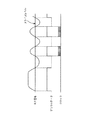
【図7】光ディスクドライブが2値化するRF信号等を説明する波形図である。
【図8】従来のジッタ計測装置の測定方法を説明する為の波形図である。
【図9】従来のジッタ計測装置の測定方法を説明する為の波形図である。
【図10】従来のジッタ計測装置の測定方法を説明する為の波形図である。
【符号の説明】
1 光ピックアップの特性検査装置、2 光学ピックアップ、3 テストベンチ、4 マトリクス回路、5 サーボコントロール回路、6 アナログ/デジタル変換回路、7 メモリ、8 コンピュータ[0001]
BACKGROUND OF THE INVENTION
The present invention relates to a jitter measurement apparatus for a reproduction signal of an optical disc for measuring a jitter component of a reproduction signal of an optical disc on which digital data is recorded according to a predetermined modulation rule, and a jitter measurement method for a reproduction signal of an optical disc. The present invention also relates to an optical disk recording and / or reproducing apparatus for reproducing an optical disk, and an optical disk reproducing method.
[0002]
[Prior art]
In an optical disk drive that reproduces an optical disk on which digital data is recorded, a reproduction (RF) signal is detected by an optical pickup, and the RF signal is binarized to generate digital data. Specifically, in the optical disc drive, the RF signal as shown in FIG. 7A is binarized at a predetermined slice level, and digital data as shown in FIG. 7B is generated.
[0003]
In general, digital data modulated in accordance with a predetermined modulation method is recorded on the optical disc. For example, in a so-called compact disc, when one period of digital data is T, a signal to be recorded is modulated into a signal having a period of 3T to 11T, and a waveform of each period is recorded at random. Further, for example, in a digital video disc, when one period of digital data is T, a recorded signal is modulated into a signal having a period of 3T to 14T, and a waveform of each period is recorded at random. . In the optical disk drive, a digital data according to such a predetermined modulation method is reproduced from an optical disk, and the signal is binarized to generate digital data.
[0004]
By the way, the digital data binarized by the optical disk drive in this way is generally reproduced in the form of noise in the period direction, that is, in the form of including a jitter component. For example, when only a waveform having a period of 3T is extracted from an RF signal reproduced from an optical disc, the period of the waveform of the RF signal is 3T ± σ (σ: jitter component) including a jitter component with respect to the theoretical period 3T. )
[0005]
The reason why the binarized digital data includes a jitter component and is reproduced is, for example, the influence of noise included in the recording signal of the optical disc or the characteristics of the optical pickup that detects the signal recorded on the optical disc. There are influences.
[0006]
Here, conventionally, a jitter measuring apparatus for detecting a jitter component of digital data reproduced from such an optical disc is known. This jitter measuring device is used to measure the jitter component of an RF signal reproduced from an optical disc and to know the characteristics of the optical disc and the characteristics of the optical pickup.
[0007]
Hereinafter, first to third jitter measuring apparatuses that have been conventionally used for measuring a jitter component of a reproduction signal of an optical disk will be described.
[0008]
The first jitter measuring apparatus conventionally used for jitter measurement is to measure the jitter component by obtaining the time width of digital data as a voltage value by an integrating circuit.
[0009]
First, in the first jitter measurement apparatus, as shown in FIG. 8, the RF signal is binarized at a predetermined slice level to generate digital data. In the first jitter measuring apparatus, the integration circuit is operated when the RF signal becomes the slice level, that is, at the rising edge of the digital data. Subsequently, in the first jitter measuring apparatus, the integration circuit is stopped when the RF signal becomes the next slice level, that is, at the falling edge of the digital data. The first jitter measuring apparatus measures the output voltage of the integrating circuit at this time as the time width of the digital data.
[0010]
Therefore, in the first jitter measuring apparatus, the jitter value (σV) converted into the voltage value can be detected by comparing the output voltage of the integrating circuit with the voltage value corresponding to the predetermined period.
[0011]
In the first jitter measuring apparatus, the characteristics of the integration circuit are determined according to the time constant, so that one integration circuit modulates one cycle among the waveforms of a plurality of cycles modulated and recorded on the optical disc. Only the jitter component corresponding to the waveform can be measured. That is, in this first jitter measuring apparatus, if the optical disc to be reproduced is a compact disc, only one jitter component of a waveform having a period of 3T is measured by one integrating circuit, and a waveform having another period, for example, 4T to 11T is measured. The jitter component of the waveform cannot be measured.
[0012]
Next, the second jitter measuring apparatus conventionally used for jitter measurement uses a so-called time interval analyzer, which counts the time width of digital data with a high-speed clock, and uses this count output as a jitter component. Is detected.
[0013]
First, in the second jitter measuring apparatus, as shown in FIG. 9, the RF signal is binarized at a predetermined slice level to generate digital data. In the second jitter measuring apparatus, the clock circuit is operated at the time when the RF signal becomes the slice level, that is, at the rising edge of the digital data, and counting of the number of clocks output from the clock circuit is started. . Subsequently, in the second jitter measuring apparatus, the clock circuit is stopped when the RF signal becomes the next slice level, that is, at the falling edge of the digital data. In the second jitter measuring apparatus, the count number at this time is the time width of the digital data.
[0014]
Therefore, in the second jitter measuring apparatus, the jitter value can be detected by comparing the count number of the counter with the count number in a predetermined period.
[0015]
Next, a third jitter measuring apparatus conventionally used for jitter measurement is an application of the first jitter measuring apparatus and the second jitter measuring apparatus.
[0016]
First, in the third jitter measuring apparatus, as shown in FIG. 10, the RF signal is binarized at a predetermined slice level to generate digital data. At this time, in the third jitter measuring apparatus, the clock circuit continues to generate a clock at a predetermined clock frequency. In the third jitter measuring apparatus, the clock circuit is operated when the RF signal reaches the slice level, that is, at the rising edge of the digital data, and the number of clocks output from the clock circuit is counted by the counter. In the third jitter measuring apparatus, the operation of the integrating circuit is started at the rising edge of the digital data. Subsequently, in the third jitter measuring apparatus, the operation of the integrating circuit is stopped at the timing of the clock generated immediately after the rising edge of the digital data. In the third jitter measuring apparatus, the output voltage V of the integrating circuit at this time1Is measured, and this output voltage V1Is converted into a time width, and the first time width t of the digital data is converted.1And
[0017]
In the third jitter measuring apparatus, the integration circuit is operated again at the clock timing immediately before the RF signal reaches the next slice level, that is, at the clock timing immediately before the falling edge of the digital data. In the third jitter measuring apparatus, the integration circuit is stopped when the RF signal becomes the next slice level, that is, at the falling edge of the digital data.
[0018]
In the third jitter measuring apparatus, the count number of the counter at the falling timing of the digital data is detected, and based on this count number and the clock frequency, the digital timing is calculated from the timing of the clock immediately after the rising edge of the digital data. The time width until the timing of the clock immediately before the falling edge of the data is obtained, and this time width is calculated as the second time width t.2And Further, in the third jitter measuring apparatus, the output voltage V of the integrating circuit at this timeThreeIs measured, and this output voltage VThreeIs converted into a time width, and the third time width t of the digital data is converted.ThreeAnd
[0019]
Therefore, in the third jitter measuring apparatus, the first time width t1, Time span t2And the above time width tThreeCan be measured as the time width of the digital data. In the third jitter measuring apparatus, the jitter value can be detected by comparing the time width of the digital data with the theoretical value.
[0020]
[Problems to be solved by the invention]
However, the conventional first to third jitter measuring apparatuses described above have the following problems.
[0021]
In the first jitter measuring apparatus, since the time width is measured in an analog manner using an integration circuit, it is difficult to stably measure the time width because it is weak against noise. In the first jitter measuring apparatus, only one jitter component of a waveform having one cycle can be measured by one integrating circuit. Therefore, in order to measure the jitter component of a waveform having a plurality of cycles, the waveform of the cycle to be measured is measured. The number of integration circuits required. That is, in the first jitter measuring apparatus, for example, nine integrating circuits having different time constants are required to detect all jitter components of a waveform having a period from 3T to 11T included in a compact disc. It was. Therefore, the hardware configuration is complicated in the first jitter measuring apparatus.
[0022]
In the second jitter measuring apparatus, since the time width is measured by counting the clock, a time width shorter than this clock cycle cannot be measured. In the second jitter measuring apparatus, since a high-speed clock is used, the processing circuit and the like are complicated, and it is difficult to reduce the cost.
[0023]
In the third jitter measuring apparatus, since the time width is measured in an analog manner using an integration circuit, it is difficult to stably measure the time width because it is weak against noise. Further, in the third jitter measuring apparatus, the circuit configuration is complicated, and the cost cannot be reduced. Since the third jitter measuring apparatus uses an integrating circuit, it requires as many integrating circuits as the number of waveforms in the period to be measured. Therefore, in the third jitter measuring apparatus, the hardware configuration is complicated in order to measure waveforms having a plurality of periods.
[0024]
The present invention has been made in view of such circumstances, and provides an optical disk reproduction signal jitter measurement apparatus, an optical disk reproduction signal jitter measurement method, an optical disk recording and / or reproduction apparatus that solve the above problems. The purpose is to provide.
[0025]
It is another object of the present invention to provide an optical disc recording and / or reproducing apparatus and an optical disc reproducing method capable of optimizing jitter components.
[0026]
[Means for Solving the Problems]
In order to solve the above-described problem, an apparatus for measuring jitter of a reproduction signal of an optical disc according to the present invention includes a predetermined modulation.Modulated according to the schemeAn analog / digital conversion means for sampling a reproduction signal of an optical disc on which digital data is recorded at a predetermined sampling frequency and converting it into digital data indicating a signal level at each sampling point, and sampling points in the vicinity of a predetermined slice level And interpolating the time point when the reproduction signal becomes the predetermined slice level based on the signal level and the sampling frequency, and determining each time width between the time point when the reproduction signal becomes the predetermined slice level,Each time width is defined as the period of each waveform included in the reproduction signal of the optical disk.Jitter calculating means for obtaining a jitter component of the reproduction signal.
[0027]
In this apparatus for measuring jitter of a reproduction signal of an optical disk, the reproduction signal of the optical disk is converted into digital data at a predetermined sampling frequency, and the time point at which the reproduction signal reaches a predetermined slice level is interpolated to obtain a jitter component of the reproduction signal.
[0028]
The jitter measurement device for the reproduction signal of the optical disk according to the present invention is such that the jitter calculation means obtains a peak value of the reproduction signal from the signal level at each sample point and sets a predetermined slice level based on the peak value. Features.
[0029]
In this apparatus for measuring the reproduction signal jitter of an optical disk, the peak value of the reproduction signal is obtained and the jitter component of the reproduction signal is obtained.
[0031]
In this apparatus for measuring jitter of a reproduction signal of an optical disk, a time width corresponding to the period of each waveform included in the reproduction signal is extracted to obtain a jitter component of the reproduction signal of the optical disk.
[0032]
In the jitter measurement device for the reproduction signal of the optical disc according to the present invention, the jitter calculation means obtains the jitter component of the reproduction signal of the optical disc, and between the time points when the reproduction signal becomes a predetermined slice level with reference to a predetermined time width. A time width corresponding to the period of each waveform included in the reproduction signal of the optical disc is extracted from each time width, and the amplitude of the reproduction signal of the waveform of each period is obtained.
[0033]
In this optical disk reproduction signal jitter measuring apparatus, the jitter component of the optical disk reproduction signal is obtained and the amplitude of the reproduction signal having a waveform of each period is obtained.
[0034]
According to the optical disk reproduction signal jitter measuring apparatus according to the present invention, the jitter calculating means obtains the jitter component of the optical disk reproduction signal and obtains the amplitude of the reproduction signal of the waveform of each period of the optical disk reproduction signal. Features.
[0035]
In this apparatus for measuring the jitter of a reproduction signal of an optical disk, the jitter component of the reproduction signal of the optical disk is obtained and the amplitude of the reproduction signal of the waveform of each period of the reproduction signal is obtained.
[0036]
A method for measuring jitter of a reproduction signal of an optical disc according to the present invention includes a predetermined modulation.Modulated according to the schemeThe reproduction signal of the optical disk on which the digital data is recorded is sampled at a predetermined sampling frequency and converted into digital data indicating the signal level at each sample point, and the signal level at the sample point near the predetermined slice level and the above Based on the sampling frequency, interpolate and determine the time point when the reproduction signal becomes the predetermined slice level, determine each time width between the time point when the reproduction signal becomes the predetermined slice level,Each time width is defined as the period of each waveform included in the reproduction signal of the optical disk.The jitter component of the reproduction signal is obtained.
[0037]
In this method for measuring the jitter of a reproduction signal of an optical disc, the reproduction signal of the optical disc is converted into digital data at a predetermined sampling frequency, and the time point at which the reproduction signal reaches a predetermined slice level is interpolated to obtain the jitter component of the reproduction signal.
[0038]
The reproduction signal jitter measurement method for an optical disk according to the present invention is characterized in that a peak value of the reproduction signal is obtained from the signal level at each sample point, and a predetermined slice level is set based on the peak value.
[0039]
In this method of measuring the jitter of a reproduction signal of an optical disc, the peak value of the reproduction signal is obtained and the jitter component of the reproduction signal is obtained.
[0040]
The method for measuring jitter of a reproduction signal of an optical disc according to the present invention includes a period of each waveform included in the reproduction signal of the optical disc from each time interval between the time points when the reproduction signal reaches a predetermined slice level with reference to the predetermined time duration. Is extracted, and a jitter component of the reproduction signal of the optical disk is obtained.
[0041]
In this method for measuring jitter of a reproduction signal of an optical disk, a time width corresponding to the period of each waveform included in the reproduction signal is extracted to obtain a jitter component of the reproduction signal of the optical disk.
[0042]
The method for measuring jitter of a reproduction signal of an optical disc according to the present invention obtains a jitter component of a reproduction signal of an optical disc, and uses a predetermined time width as a reference from each time width between times when the reproduction signal becomes a predetermined slice level. A time width corresponding to the period of each waveform included in the reproduction signal of the optical disk is extracted, and the amplitude of the reproduction signal of the waveform of each period is obtained.
[0043]
In this method of measuring the jitter of the reproduction signal of the optical disk, the jitter component of the reproduction signal of the optical disk is obtained and the amplitude of the reproduction signal having a waveform of each period is obtained.
[0044]
The jitter measurement method for the reproduction signal of the optical disc according to the present invention is characterized in that the jitter component of the reproduction signal of the optical disc is obtained, and the amplitude of the reproduction signal of the waveform of each period of the reproduction signal of the optical disc is obtained.
[0045]
In this method of measuring the jitter of a reproduction signal of an optical disc, the jitter component of the reproduction signal of the optical disc is obtained, and the amplitude of the reproduction signal of the waveform of each period of the reproduction signal is obtained.
[0046]
An optical disk recording and / or reproducing apparatus according to the present invention has a predetermined modulation.Modulated according to the schemeA reproducing means for reproducing an optical disk on which digital data is recorded and outputting data corresponding to the recorded signal, and a reproduction signal reproduced by the reproducing means are sampled at a predetermined sampling frequency, Analog / digital conversion means for converting into digital data indicating the signal level, and interpolating the time when the reproduction signal becomes the predetermined slice level based on the signal level and the sampling frequency at the sample points near the predetermined slice level. Obtaining each time width between the time points when the reproduction signal becomes the predetermined slice level,Each time width is defined as the period of each waveform included in the reproduction signal of the optical disk.Jitter calculation control means for obtaining a jitter component of the reproduction signal and controlling the reproduction means based on the jitter component.
[0047]
In this optical disk recording and / or reproducing apparatus, the reproduction signal of the optical disk is converted into digital data at a predetermined sampling frequency, the time when the reproduction signal becomes a predetermined slice level is interpolated, and the jitter component of the reproduction signal is obtained. The reproduction signal is feedback controlled based on the jitter component.
[0048]
An optical disc reproducing method according to the present invention comprises a predetermined modulation.Modulated according to the schemeThe optical disk on which the digital data is recorded is reproduced, data corresponding to the recorded signal is output, and the reproduction signal of the optical disk on which the digital data in accordance with the predetermined modulation rule is recorded at a predetermined sampling frequency. Sampling and converting into digital data indicating the signal level at each sample point, and a point in time when the reproduction signal becomes the predetermined slice level based on the signal level and the sampling frequency at a sample point near the predetermined slice level Obtained by interpolating, obtaining each time width between the time points when the reproduction signal becomes the predetermined slice level,Each time width is defined as the period of each waveform included in the reproduction signal of the optical disk.A jitter component of the reproduction signal is obtained, and reproduction characteristics of the optical disc are controlled based on the jitter component.
[0049]
In this optical disk reproduction method, the reproduction signal of the optical disk is converted into digital data at a predetermined sampling frequency, the time point at which the reproduction signal reaches a predetermined slice level is interpolated, and the jitter component of the reproduction signal is obtained, and based on this jitter component Feedback control of the playback signal.
[0050]
DETAILED DESCRIPTION OF THE INVENTION
Hereinafter, embodiments of the present invention will be described with reference to the drawings.
[0051]
An optical pickup characteristic measurement apparatus (hereinafter simply referred to as a characteristic inspection apparatus) according to an embodiment of the present invention measures the characteristic of a jitter component of an optical pickup used in an optical disk drive. Such a characteristic inspection apparatus is used for inspection of specifications of the optical pickup, inspection of characteristics of the optical pickup, and the like, for example, shipping inspection and acceptance inspection of the optical pickup.
[0052]
FIG. 1 is a block diagram of a characteristic inspection apparatus according to an embodiment of the present invention.
[0053]
The
[0054]
The
[0055]
Further, the
[0056]
The
[0057]
The
[0058]
For example, the
[0059]
Each of the photodetectors A to F converts the amount of the reflected light that has been irradiated into signals A to F. The
[0060]
The
[0061]
The matrix circuit 4 is supplied with signals A to F which are the outputs of the photodetectors A to F of the
[0062]
Further, digital data modulated according to a predetermined modulation method is recorded on the optical disc. For example, in a so-called compact disc, when one period of digital data is T, a signal having a period of 3T to 11T is recorded at random. Further, in the digital video disc, a signal having a period of 3T to 14T is randomly recorded, where T is one period of digital data. Digital data in accordance with such a predetermined modulation method is generated by binarizing the RF signal generated by the matrix circuit 4 at a predetermined slice level.
[0063]
The matrix circuit 4 supplies the RF signal, FE signal, and TE signal thus calculated to the servo control circuit 5. The matrix circuit 4 supplies the RF signal to the analog / digital conversion circuit 6.
[0064]
The servo control circuit 5 performs servo control when reproducing and driving the optical disk based on the RF signal, the FE signal, and the TE signal. Specifically, the servo control circuit 5 performs a focus servo control by driving a biaxial actuator that operates the objective lens of the
[0065]
The analog / digital conversion circuit 6 is fast enough to sufficiently reproduce a waveform having a minimum theoretical period of digital data in accordance with a predetermined modulation method generated from an RF signal, for example, a 3T period waveform in the case of a compact disk. The RF signal is sampled at the sampling frequency. The analog / digital conversion circuit 6 converts the RF signal into digital data at a sampling frequency of about 30 MHz, for example. The analog / digital conversion circuit 6 supplies the RF signal converted into digital data to the
[0066]
The
[0067]
The
[0068]
The arithmetic processing unit 8d of the
[0069]
In addition, the arithmetic processing unit 8 d of the
[0070]
Next, the measurement processing contents of the jitter component of the
[0071]
When the
[0072]
In step S1, the
[0073]
Subsequently, in step S2, the
[0074]
Subsequently, in step S3, the
[0075]
In the peak value detection process in step S3, the arithmetic processing unit 8d reads the quantized data stored in the
[0076]
Subsequently, in step S4, the
[0077]
For example, the
[0078]
Further, when calculating the slice level, the
[0079]
For example, the
[0080]
In setting the slice level, the
[0081]
Subsequently, in step S5, the
[0082]
Subsequently, in step S6, the
[0083]
If the
[0084]
Subsequently, in step S7, the
[0085]
Hereinafter, the step S7 will be specifically described by taking as an example the case of calculating the time width of a part of the waveform X shown in FIG. 5B among the RF signals as shown in FIG.
[0086]
As shown in FIG. 6, the
[0087]
First, in step S11, the
[0088]
Subsequently, in step S12, the
[0089]
Subsequently, in step S13, the
[0090]
In step S12 and step S13, any calculation method for interpolating quantized data for obtaining the RF signal times P1 and P2 at the slice level may be used. For example, linear interpolation may be used. You may ask for it. Further, if quantized data in the vicinity of the slice level is used, it is not necessary to obtain from the two quantized data. For example, the time when the RF signal is at the slice level may be obtained from three data or four data. .
[0091]
Subsequently, in step S14, the
[0092]
Subsequently, in step S15, the
[0093]
Subsequently, in step S16, the
[0094]
Subsequently, in step S17, the
[0095]
As described above, in the
[0096]
Further, in step S7, the
[0097]
Subsequently, in step S8, the
[0098]
In this way, the
[0099]
Subsequently, in step S9, the
[0100]
For example, the
In equation (1), ni is the length of each waveform of the reproduction signal, and an arbitrary value in the period 3T to 11T (T is one period of the digital data)
[0101]
σ = √ (Σniσi 2 / Σni(1)
As described above, the
[0102]
Further, the arithmetic processing unit 8d adds the measurement result of the jitter component as an offset component to a control amount such as a focus servo. The characteristic inspection /
[0103]
As described above, in the
[0104]
In the
[0105]
In the
[0106]
The
[0107]
That is, the
[0108]
Further, in the
[0109]
Although the
[0110]
In addition, the
[0111]
Furthermore, the
[0112]
The present invention also includes the analog / digital conversion circuit 6, the
[0113]
That is, such an optical disk recording and / or reproducing apparatus has an analog / digital conversion circuit to which an output of an optical pickup reproduction signal is supplied and an output of the analog / digital conversion circuit in addition to the circuit configuration of a normal optical disk An arithmetic processing unit that calculates characteristics of a reproduction signal and the like is provided.
[0114]
The arithmetic processing unit is composed of, for example, a digital signal processor and measures the jitter component as described above from the output data of the analog / digital conversion circuit. Based on the measurement result, the arithmetic processing unit controls the reproduction circuit and the like so that the servo characteristics and reproduction characteristics of the recording and / or reproduction apparatus are optimized. The optical disc recording / reproducing apparatus can reproduce the optical disc under optimum reproduction conditions.
[0115]
【The invention's effect】
The apparatus for measuring jitter of a reproduction signal of an optical disc according to the present invention converts the reproduction signal of an optical disc into digital data at a predetermined sampling frequency, interpolates the time point at which the reproduction signal reaches a predetermined slice level, and generates a jitter component of the reproduction signal. Ask.
[0116]
As a result, the jitter measurement apparatus for the reproduction signal of the optical disk can measure the jitter component stably against noise. Further, the jitter measurement apparatus for the reproduction signal of the optical disc according to the present invention can measure the jitter component for each period included in the reproduction signal. Further, the jitter measurement apparatus for the reproduction signal of the optical disc according to the present invention can determine the total jitter component included in the reproduction signal having the waveform of all the periods.
[0117]
In the method for measuring jitter of a reproduction signal of an optical disk according to the present invention, the reproduction signal of the optical disk is converted into digital data at a predetermined sampling frequency, the time point at which the reproduction signal reaches a predetermined slice level is interpolated, and the jitter component of the reproduction signal is calculated. Ask.
[0118]
As a result, the jitter measurement method of the reproduction signal of the optical disc can measure the jitter component stably against noise. Furthermore, in the method for measuring jitter of a reproduction signal of an optical disc according to the present invention, a jitter component can be measured for each period included in the reproduction signal. In the method for measuring jitter of a reproduction signal of an optical disk according to the present invention, the total jitter component included in the reproduction signal having a waveform having all periods can be obtained.
[0119]
In the optical disk recording and / or reproducing apparatus according to the present invention, the reproduction signal of the optical disk is converted into digital data at a predetermined sampling frequency, the time point at which the reproduction signal reaches a predetermined slice level is interpolated, and the jitter component of the reproduction signal is obtained. The reproduced signal is feedback-controlled based on the jitter component.
[0120]
As a result, the optical disk recording and / or reproducing apparatus according to the present invention can reproduce the optical disk under optimum reproduction conditions.
[0121]
In the optical disk reproduction method according to the present invention, the reproduction signal of the optical disk is converted into digital data at a predetermined sampling frequency, the time point at which the reproduction signal reaches a predetermined slice level is interpolated, and the jitter component of the reproduction signal is obtained. The reproduction signal is feedback controlled based on the components.
[0122]
As a result, the optical disc playback method according to the present invention can play back an optical disc under optimum playback conditions.
[Brief description of the drawings]
FIG. 1 is a block configuration diagram of a characteristic inspection apparatus for an optical pickup according to an embodiment of the present invention.
FIG. 2 is a diagram illustrating an example of a photodetector provided in an optical pickup which is an inspection target of the optical pickup characteristic inspection apparatus.
FIG. 3 is a flowchart for explaining processing contents of the optical pickup characteristic inspection apparatus;
FIG. 4 is a waveform diagram for explaining processing contents of the optical pickup characteristic inspection apparatus;
FIG. 5 is a waveform diagram for explaining processing contents of the characteristic inspection apparatus for the optical pickup;
FIG. 6 is a flowchart for explaining the processing content of the optical pickup characteristic inspection apparatus;
FIG. 7 is a waveform diagram for explaining an RF signal or the like that is binarized by the optical disk drive.
FIG. 8 is a waveform diagram for explaining a measurement method of a conventional jitter measurement apparatus.
FIG. 9 is a waveform diagram for explaining a measurement method of a conventional jitter measurement apparatus.
FIG. 10 is a waveform diagram for explaining a measurement method of a conventional jitter measurement apparatus.
[Explanation of symbols]
1 Optical pickup characteristic inspection device, 2 Optical pickup, 3 Test bench, 4 Matrix circuit, 5 Servo control circuit, 6 Analog / digital conversion circuit, 7 Memory, 8 Computer
Claims (28)
所定のスライスレベルの近傍のサンプル点における上記信号レベル及び上記サンプリング周波数に基づき上記再生信号が上記所定のスライスレベルとなる時点を補間して求め、上記再生信号が上記所定のスライスレベルとなる時点間の各時間幅を求め、上記各時間幅を光ディスクの再生信号に含まれる各波形の周期として光ディスクの再生信号のジッタ成分を求めるジッタ演算手段とを備える光ディスクの再生信号のジッタ計測装置。An analog / digital conversion means for sampling a reproduction signal of an optical disc on which digital data modulated in accordance with a predetermined modulation method is recorded at a predetermined sampling frequency and converting the sampled signal into digital data indicating a signal level at each sample point;
Based on the signal level and the sampling frequency at a sample point in the vicinity of a predetermined slice level, the time when the reproduction signal becomes the predetermined slice level is interpolated to obtain the interval between the time when the reproduction signal becomes the predetermined slice level. And a jitter calculating means for obtaining a jitter component of the reproduction signal of the optical disk by using each time width as a period of each waveform included in the reproduction signal of the optical disk.
σ=√(Σniσi2/Σni) ・・・(1)
σ:全ての周期の波形の再生信号に基づき求められたジッタ成分
σi:1の周期の波形の再生信号に基づき求められたジッタ成分
ni:再生信号の各波形の長さであり、周期3T〜11Tの任意の値(Tは上記デジタルデータの1周期) 12. The apparatus for measuring jitter of a reproduction signal of an optical disc according to claim 11, wherein the jitter calculating means obtains a jitter component using the following equation (1).
σ = √ (Σniσi2 / Σni) (1)
σ: Jitter component obtained based on a reproduction signal having a waveform of all periods σi: Jitter component obtained based on a reproduction signal having a waveform having a period of σi: 1
ni: the length of each waveform of the reproduction signal, and an arbitrary value in the period 3T to 11T (T is one period of the digital data)
所定のスライスレベルの近傍のサンプル点における上記信号レベル及び上記サンプリング周波数に基づき上記再生信号が上記所定のスライスレベルとなる時点を補間して求め、
上記再生信号が上記所定のスライスレベルとなる時点間の各時間幅を求め、
上記各時間幅を光ディスクの再生信号に含まれる各波形の周期として光ディスクの再生信号のジッタ成分を求めることを特徴とする光ディスクの再生信号のジッタ計測方法。A reproduction signal of an optical disc on which digital data modulated in accordance with a predetermined modulation method is recorded, sampled at a predetermined sampling frequency, and converted into digital data indicating a signal level at each sample point,
Based on the signal level at the sample point in the vicinity of the predetermined slice level and the sampling frequency, interpolated to determine the time point when the reproduction signal becomes the predetermined slice level,
Each time width between the time points when the reproduction signal becomes the predetermined slice level is obtained,
A jitter measurement method for an optical disk reproduction signal, wherein a jitter component of the reproduction signal of the optical disk is obtained by using each time width as a period of each waveform included in the reproduction signal of the optical disk.
σ=√(Σniσi2/Σni) ・・・(2)
σ:全ての周期の波形の再生信号に基づき求められたジッタ成分
σi:1の周期の波形の再生信号に基づき求められたジッタ成分
ni:再生信号の各波形の長さであり、周期3T〜11Tの任意の値(Tは上記デジタルデータの1周期) The method for measuring jitter of a reproduction signal of an optical disk according to claim 23 , wherein a jitter component is obtained using the following equation (2).
σ = √ (Σniσi2 / Σni) (2)
σ: Jitter component obtained based on a reproduction signal having a waveform of all periods σi: Jitter component obtained based on a reproduction signal having a waveform having a period of σi: 1
ni: the length of each waveform of the reproduction signal, and an arbitrary value in the period 3T to 11T (T is one period of the digital data)
上記再生手段が再生した再生信号を、所定のサンプリング周波数でサンプルして各サンプル点での信号レベルを示すデジタルデータに変換するアナログ/デジタル変換手段と、
所定のスライスレベルの近傍のサンプル点における上記信号レベル及び上記サンプリング周波数に基づき上記再生信号が上記所定のスライスレベルとなる時点を補間して求め、上記再生信号が上記所定のスライスレベルとなる時点間の各時間幅を求め、上記各時間幅を光ディスクの再生信号に含まれる各波形の周期として光ディスクの再生信号のジッタ成分を求め、このジッタ成分に基づき上記再生手段を制御するジッタ演算制御手段と
を備える光ディスクの記録及び/又は再生装置。Reproducing means for reproducing an optical disc on which digital data modulated in accordance with a predetermined modulation method is recorded, and outputting data corresponding to the recorded signal;
Analog / digital conversion means for sampling a reproduction signal reproduced by the reproduction means at a predetermined sampling frequency and converting the sampled signal into digital data indicating a signal level at each sampling point;
Based on the signal level and the sampling frequency at a sample point in the vicinity of a predetermined slice level, the time when the reproduction signal becomes the predetermined slice level is interpolated to obtain the interval between the time when the reproduction signal becomes the predetermined slice level. A jitter calculation control means for obtaining a jitter component of the reproduction signal of the optical disk by using each time width as a period of each waveform included in the reproduction signal of the optical disk and controlling the reproduction means based on the jitter component; An optical disc recording and / or reproducing apparatus comprising:
上記所定の変調規則に従ったデジタルデータが記録された光ディスクの再生信号を、所定のサンプリング周波数でサンプルして各サンプル点での信号レベルを示すデジタルデータに変換し、
所定のスライスレベルの近傍のサンプル点における上記信号レベル及び上記サンプリング周波数に基づき上記再生信号が上記所定のスライスレベルとなる時点を補間して求め、
上記再生信号が上記所定のスライスレベルとなる時点間の各時間幅を求め、
上記各時間幅を光ディスクの再生信号に含まれる各波形の周期として光ディスクの再生信号のジッタ成分を求め、
上記ジッタ成分に基づき、光ディスクの再生特性を制御することを特徴とする光ディスクの再生方法。Playing back an optical disc on which digital data modulated according to a predetermined modulation method is recorded, and outputting data according to the recorded signal,
A reproduction signal of an optical disc on which digital data according to the predetermined modulation rule is recorded is sampled at a predetermined sampling frequency and converted into digital data indicating a signal level at each sample point,
Based on the signal level at the sample point in the vicinity of the predetermined slice level and the sampling frequency, interpolated to determine the time point when the reproduction signal becomes the predetermined slice level,
Each time width between the time points when the reproduction signal becomes the predetermined slice level is obtained,
Using each time width as the period of each waveform included in the reproduction signal of the optical disk, the jitter component of the reproduction signal of the optical disk is obtained,
A method for reproducing an optical disc, wherein the reproduction characteristic of the optical disc is controlled based on the jitter component.
Applications Claiming Priority (2)
| Application Number | Priority Date | Filing Date | Title |
|---|---|---|---|
| SG1997003386A SG65019A1 (en) | 1997-09-13 | 1997-09-13 | Jitter measuring method utilizing a/d conversion and device |
| SG9703386-4 | 1997-09-13 |
Publications (2)
| Publication Number | Publication Date |
|---|---|
| JPH11183325A JPH11183325A (en) | 1999-07-09 |
| JP3860344B2 true JP3860344B2 (en) | 2006-12-20 |
Family
ID=20429731
Family Applications (1)
| Application Number | Title | Priority Date | Filing Date |
|---|---|---|---|
| JP25880198A Expired - Fee Related JP3860344B2 (en) | 1997-09-13 | 1998-09-11 | Optical disk reproduction signal jitter measurement apparatus, optical disk reproduction signal jitter measurement method, optical disk recording and / or reproduction apparatus, and optical disk reproduction method |
Country Status (5)
| Country | Link |
|---|---|
| US (1) | US6366631B1 (en) |
| JP (1) | JP3860344B2 (en) |
| CN (1) | CN1143281C (en) |
| SG (1) | SG65019A1 (en) |
| TW (1) | TW408225B (en) |
Families Citing this family (22)
| Publication number | Priority date | Publication date | Assignee | Title |
|---|---|---|---|---|
| US7012872B2 (en) | 2000-01-07 | 2006-03-14 | Funai Electric Co., Ltd. | Image reading device for an optical device |
| GB2368651B (en) * | 2000-10-31 | 2006-05-31 | Consultronics Europ Ltd | Method and apparatus for measurement of jitter |
| JP2002269925A (en) * | 2001-03-09 | 2002-09-20 | Matsushita Electric Ind Co Ltd | Optical disk playback device |
| JP4124407B2 (en) * | 2001-09-13 | 2008-07-23 | 株式会社リコー | Binarization device |
| CN100346399C (en) * | 2002-04-03 | 2007-10-31 | 松下电器产业株式会社 | Optical disk drive, optical storage medium, optical storage medium inspection device, and optical storage inspection method |
| US7519874B2 (en) * | 2002-09-30 | 2009-04-14 | Lecroy Corporation | Method and apparatus for bit error rate analysis |
| US20040123018A1 (en) * | 2002-09-30 | 2004-06-24 | Martin Miller | Method and apparatus for analyzing serial data streams |
| US7437624B2 (en) * | 2002-09-30 | 2008-10-14 | Lecroy Corporation | Method and apparatus for analyzing serial data streams |
| WO2004036231A2 (en) * | 2002-10-18 | 2004-04-29 | Lecroy Corporation | Method and apparatus for determining inter-symbol interference for estimating data dependent jitter |
| US7627790B2 (en) * | 2003-08-21 | 2009-12-01 | Credence Systems Corporation | Apparatus for jitter testing an IC |
| KR100594246B1 (en) * | 2004-02-06 | 2006-06-30 | 삼성전자주식회사 | Servo timing jitter compensation method and apparatus and disk drive using same |
| GB0412451D0 (en) * | 2004-06-04 | 2004-07-07 | Koninkl Philips Electronics Nv | Measuring clock jitter |
| US7286947B1 (en) | 2006-04-13 | 2007-10-23 | International Business Machines Corporation | Method and apparatus for determining jitter and pulse width from clock signal comparisons |
| US7389192B2 (en) * | 2006-06-30 | 2008-06-17 | International Business Machines Corporation | Determining data signal jitter via asynchronous sampling |
| US7684478B2 (en) * | 2006-06-30 | 2010-03-23 | International Business Machines Corporation | Generating an eye diagram of integrated circuit transmitted signals |
| US7383160B1 (en) * | 2006-06-30 | 2008-06-03 | International Business Machines Corporation | Method and apparatus for constructing a synchronous signal diagram from asynchronously sampled data |
| US8616641B2 (en) * | 2006-10-04 | 2013-12-31 | Access Enterprise, Llc | Therapeutic back support and stabilization |
| US7953320B2 (en) * | 2008-03-20 | 2011-05-31 | Avago Technologies Fiber Ip (Singapore) Pte. Ltd. | Systems and methods for determining an AC/DC cross-calibration coefficient |
| JP5131485B2 (en) * | 2009-07-23 | 2013-01-30 | パルステック工業株式会社 | Apparatus and method for measuring pulse width and jitter |
| US9354266B2 (en) | 2012-06-07 | 2016-05-31 | Globalfoundries Inc. | Universal jitter meter and phase noise measurement |
| US9568548B1 (en) | 2015-10-14 | 2017-02-14 | International Business Machines Corporation | Measurement of signal delays in microprocessor integrated circuits with sub-picosecond accuracy using frequency stepping |
| CN114726437B (en) * | 2022-06-08 | 2022-10-14 | 电子科技大学 | Digital optical transmitter edge jitter detector |
Family Cites Families (4)
| Publication number | Priority date | Publication date | Assignee | Title |
|---|---|---|---|---|
| JP3510015B2 (en) * | 1995-09-11 | 2004-03-22 | 株式会社日立製作所 | Optical disk recording and playback device |
| US5848036A (en) * | 1996-06-20 | 1998-12-08 | Matsushita Electric Industrial Co., Ltd. | Optical disk drive equipped with waveform equalizer and focus adjustment circuit |
| US5978335A (en) * | 1996-06-28 | 1999-11-02 | Ibm | Integrated calibration apparatus for a multi-mode information storage system |
| JP3915163B2 (en) * | 1997-03-18 | 2007-05-16 | ソニー株式会社 | Digital signal regeneration circuit |
-
1997
- 1997-09-13 SG SG1997003386A patent/SG65019A1/en unknown
-
1998
- 1998-09-11 JP JP25880198A patent/JP3860344B2/en not_active Expired - Fee Related
- 1998-09-11 US US09/150,970 patent/US6366631B1/en not_active Expired - Fee Related
- 1998-09-13 CN CNB981203779A patent/CN1143281C/en not_active Expired - Fee Related
- 1998-09-30 TW TW087116265A patent/TW408225B/en active
Also Published As
| Publication number | Publication date |
|---|---|
| CN1143281C (en) | 2004-03-24 |
| US6366631B1 (en) | 2002-04-02 |
| JPH11183325A (en) | 1999-07-09 |
| CN1221175A (en) | 1999-06-30 |
| TW408225B (en) | 2000-10-11 |
| SG65019A1 (en) | 1999-09-21 |
Similar Documents
| Publication | Publication Date | Title |
|---|---|---|
| JP3860344B2 (en) | Optical disk reproduction signal jitter measurement apparatus, optical disk reproduction signal jitter measurement method, optical disk recording and / or reproduction apparatus, and optical disk reproduction method | |
| JPH09245357A (en) | Servo control device for optical disk recording / reproducing apparatus | |
| JPH11154337A (en) | Device and method for measuring optical pickup and/or optical disk characteristic, optical disk recording and/or reproducing device and optical disk reproducing method | |
| JPH11161978A (en) | Focusing characteristic measuring device of optical pickup and/or optical disk, measuring method thereof, optical disk recording and/or reproducing device and method thereof | |
| KR100731245B1 (en) | Optical disc apparatus and optical disc evaluating method | |
| JP4083993B2 (en) | AR measuring apparatus for optical recording medium having pre-pits | |
| JP2003317274A (en) | Optical disk unit | |
| JP2003085789A (en) | Optical disk drive | |
| KR100521666B1 (en) | Jitter measuring method utilizing A/D conversion and device | |
| JPH10268015A (en) | Device for generating calibration signal for measuring jitter | |
| KR100653300B1 (en) | Optical disc device and optical disc evaluation method | |
| JPH07262584A (en) | Optical pickup device | |
| KR100388003B1 (en) | Optical information reproducing device | |
| KR100244773B1 (en) | How to adjust the offset of the optical disc player | |
| JP2766178B2 (en) | Mirror signal detection method and circuit for optical disk device | |
| JP3240462B2 (en) | Optical pickup servo device for optical disk drive | |
| KR100696757B1 (en) | Optimal Recording Power Detection Apparatus and Method in Optical Recording Apparatus | |
| JP4048519B2 (en) | Jitter measuring device | |
| JP2000082230A (en) | Optical disk device | |
| JP2005310256A (en) | Information recording method and information recording apparatus | |
| JPH05114145A (en) | Optical disk device | |
| JP2003323728A (en) | Recording and/or reproducing method of optical disk, and its method | |
| JPH07235055A (en) | Method for setting recording laser beam for optical disk and optical disk recording/reproducing device | |
| KR0165598B1 (en) | Tracking servo control device of optic disk reproducing system | |
| KR100509663B1 (en) | Apparatus for measuring characteristics of optical disc systems and method |
Legal Events
| Date | Code | Title | Description |
|---|---|---|---|
| A131 | Notification of reasons for refusal |
Free format text: JAPANESE INTERMEDIATE CODE: A131 Effective date: 20050823 |
|
| A521 | Request for written amendment filed |
Free format text: JAPANESE INTERMEDIATE CODE: A523 Effective date: 20051124 |
|
| TRDD | Decision of grant or rejection written | ||
| A01 | Written decision to grant a patent or to grant a registration (utility model) |
Free format text: JAPANESE INTERMEDIATE CODE: A01 Effective date: 20060822 |
|
| A61 | First payment of annual fees (during grant procedure) |
Free format text: JAPANESE INTERMEDIATE CODE: A61 Effective date: 20060921 |
|
| R150 | Certificate of patent or registration of utility model |
Free format text: JAPANESE INTERMEDIATE CODE: R150 |
|
| FPAY | Renewal fee payment (event date is renewal date of database) |
Free format text: PAYMENT UNTIL: 20100929 Year of fee payment: 4 |
|
| LAPS | Cancellation because of no payment of annual fees |