JP3857757B2 - Integrated circuit test equipment - Google Patents
Integrated circuit test equipment Download PDFInfo
- Publication number
- JP3857757B2 JP3857757B2 JP30078796A JP30078796A JP3857757B2 JP 3857757 B2 JP3857757 B2 JP 3857757B2 JP 30078796 A JP30078796 A JP 30078796A JP 30078796 A JP30078796 A JP 30078796A JP 3857757 B2 JP3857757 B2 JP 3857757B2
- Authority
- JP
- Japan
- Prior art keywords
- test
- lead
- integrated circuit
- delay
- data
- Prior art date
- Legal status (The legal status is an assumption and is not a legal conclusion. Google has not performed a legal analysis and makes no representation as to the accuracy of the status listed.)
- Expired - Fee Related
Links
Images


Classifications
-
- G—PHYSICS
- G01—MEASURING; TESTING
- G01R—MEASURING ELECTRIC VARIABLES; MEASURING MAGNETIC VARIABLES
- G01R31/00—Arrangements for testing electric properties; Arrangements for locating electric faults; Arrangements for electrical testing characterised by what is being tested not provided for elsewhere
- G01R31/28—Testing of electronic circuits, e.g. by signal tracer
- G01R31/317—Testing of digital circuits
- G01R31/3181—Functional testing
- G01R31/319—Tester hardware, i.e. output processing circuits
- G01R31/31903—Tester hardware, i.e. output processing circuits tester configuration
- G01R31/31907—Modular tester, e.g. controlling and coordinating instruments in a bus based architecture
-
- G—PHYSICS
- G01—MEASURING; TESTING
- G01R—MEASURING ELECTRIC VARIABLES; MEASURING MAGNETIC VARIABLES
- G01R31/00—Arrangements for testing electric properties; Arrangements for locating electric faults; Arrangements for electrical testing characterised by what is being tested not provided for elsewhere
- G01R31/28—Testing of electronic circuits, e.g. by signal tracer
- G01R31/317—Testing of digital circuits
- G01R31/3181—Functional testing
- G01R31/319—Tester hardware, i.e. output processing circuits
Landscapes
- Engineering & Computer Science (AREA)
- General Engineering & Computer Science (AREA)
- Physics & Mathematics (AREA)
- General Physics & Mathematics (AREA)
- Tests Of Electronic Circuits (AREA)
- Test And Diagnosis Of Digital Computers (AREA)
Description
【0001】
【発明の属する技術分野】
本発明は、集積回路テスト装置に関し、より詳細には非常に速いクロック速度でテストする集積回路テスト装置に関する。
【0002】
【発明が解決しようとする課題】
集積回路デバイスを製造するとき、これらのデバイスはシリコンウェハーの大型基板の上に多数つくられる。個々の集積回路デバイスは大型シリコンウェハーから切断される。得られた各デバイスは、デバイス仕様によって決まる目的を持った独自のチップである。個々のデバイスが仕様通りに機能できないという可能性がある。このような不良デバイスを識別するには、そのデバイスに一連のテストを実行して、そのデバイス独自の仕様を満足することを検証する。テストするデバイスは、マイクロプロセッサ、メモリあるいはモジュールでもよい。
【0003】
現在でも集積回路をテストするためには、テスト装置とテスト手順が使用されるが、これらのテスト装置やテスト手順は約15年前に使用されたものと非常によく似ている。電子機器の大型の箱、つまりテスタにはドライバとクロックエッジコントローラを備えたテスタ論理が含まれている。ドライバの出力は、同軸ケーブルを介してテスト盤のデバイスソケットに接続されている。テストするためには、集積回路デバイスをソケットに挿入する。1つのテスタに制御されて一度にいくつかのデバイスをテストすることができれば、テスタの時間を節約することになる。テスタにはそれぞれ約2百万ドルの費用がかかるから、テスタの時間を節約できることは重要である。
【0004】
普通、テスタには中央処理装置が含まれており、この中央処理装置は、電気的にレジスタと接続されるいくつかのアルゴリズム発生器を制御する。これらのレジスタは、データパルスの正確なタイミングを保証するエッジコントローラの制御のもとにデバイスにデータを出力する。中央処理装置は、デバイスに対して所期のテストを実行する完全なプログラミング能力を備えている。いくつかの集積回路のテストを並行して実行するため、十分なメモリ、モニタ、ハードディスク、エントリシステムが備えられている。テスタのドライバは、長さが数十センチメートルあってもよいケーブルを介してレベル変換器に接続されている。このレベル変換器は、これも長さが数十センチメートルあってもよい別のケーブルを介してテスト盤のソケットに接続されている。
【0005】
テスタが10MHzで動作している場合、接続ケーブルの長さが重要になることはない。たとえば、同軸ケーブルの長さが約3センチメートル異なると、100ナノセコンドのタイムスロットにおいて100ピコセコンドの差が生じるが、全部ではないにせよ、ほとんどのテストに対してこの差は無視できるかまたは意味を持たない。
【0006】
テストするデバイスによっては、パッケージに組込む前または後でテストを実行することができる。ある種の集積回路は、組立の前と後でテストされる。テストにはいろいろなタイプがある。パワーテストは、短絡回路または他の低インピーダンスの故障のためデバイスが燃えてしまわないことを検証する。機能テストは、デバイスがデバイス仕様通りに機能することを検証する。スピードテストは、デバイスが指定された速度で動作することを検証する。また外部電源からの入力、タイミング、バイアス電圧を変えて、デバイスがそのデバイス仕様で許される変動に耐えるかどうかを調べる。
【0007】
現在のところ、既存のテスタを調整して、より速くより速いスピードでテストを実行するするようにしている。性能を向上した新型テスタを使用しなければならないときは、いつも以前のテストスピードよりも約20パーセント以上クロックスピードが速められる。このようにテストスピードを速くするには、高額で望ましくない取替え投資が必要になる。
【0008】
新しく設計されるデバイスは、250MHzのクロックでかつ4ナノセコンドのタイムスロットで動作する。これらのデバイスには、1ナノセコンドのセットアップ時間と保持時間がある。ケーブルの長さが3センチメートル変わると、タイムスロットの中で100ピコセコンドの差が生じることを前に述べた。この差はタイムスロットの約10パーセントであるから、非常に重要な意味を持つことになる。
【0009】
近い将来において、デバイスは、2ナノセコンドのタイムスロットを使用して、さらに高速で動作するであろう。そうするとケーブルの長さに前記の差があると、タイムスロットに20パーセントから25パーセントの変化が生じることになる。それだけ変化すると、デバイスを効率的にテストできるか否かが問題になる。これは、タイミングの問題とともにテスタの取替え費用に対する解決策を必要とする課題である。
【0010】
【課題を解決する手段】
これらの課題は、複数のマイクロコンピュータを含む集積回路デバイステスト装置によって解決される。各マイクロコンピュータは、個別のテストソケットを介して、テストソケットに挿入されている個別の集積回路デバイスに直接結合される。集積回路デバイステスタは、複数のマイクロコンピュータに呼出されて、デバイステスタと複数のマイクロコンピュータとの間で情報を送る。各マイクロコンピュータは、対応する集積回路デバイスに関するテストルーチンを実行し、テストルーチンの結果を選択してテスタに送る命令とデータとを含んでいる。
【0011】
【発明の実施の形態】
添付の図面を参照して、本発明の実施例に関する以下の詳細な説明を読むことにより本発明をより良く理解することができるであろう。
【0012】
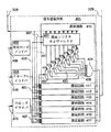
図1を参照すると、それぞれテストソケット30、31に挿入または搭載された集積回路デバイス24、25を含む集積回路デバイステスタ20が示されている。テストソケット30、31は、テストハンドラ盤35の1側に取付られている。テストハンドラ盤35の他側にはマイクロコンピュータソケット40、41があり、入出力バッファ48、49とともにマイクロコンピュータデバイス44、45がそれぞれ挿入されている。マイクロコンピュータ44、45に固有なリード線が、それぞれマイクロコンピュータソケット40、41とテストソケット30、31とを介して集積回路デバイス24、25に接続されている。マイクロコンピュータの位置の間に複数の破線が示されているが、これらの破線は、マイクロコンピュータと集積回路デバイスとがシリアルループ構成で挿入できることを示している。マイクロコンピュータとテストされる集積回路の総数が非常に大きな数になり得るという利点がある。
【0013】
また図1には、パーソナルコンピュータあるいはワークステーション55、クロック分配ブロック58、電源装置62、スケーラブルコヒーレントインタフェース(scalable coherent interface:以下SCIを使用する)リンク70、72、74、76、SCIドライバ装置80も示されている。SCIリンクは、シリアルループ構成における主要な構成部分の間を高速でポイントツーポイント接続する複数のリンクを提供する。クロック分配ブロック58はリード線85を介してテストソケット30、31にクロック信号を供給する。また電源装置62はリード線87を介してテストソケット30、31に外部の電圧を供給する。
【0014】
パーソナルコンピュータあるいはワークステーション55は、テストノードN1からNnのすべてを制御する完全な中央処理能力を備えており、集積回路デバイスに対して所期のテストを実行する。中央プロセッサはSCIを介して各テストノードの各マイクロコンピュータにアルゴリズム情報を伝達することを制御する。中央プロセッサは、所期のアルゴリズム情報を提供することができる。アルゴリズム動作を制御するためには、十分なメモリ、ハードディスク容量、モニタ、エントリシステムが含まれていなければならない。各マイクロコンピュータに適切なアルゴリズム情報が伝達される。テストする集積回路デバイスがすべて同じである場合は、全テストノードの各マイクロコンピュータに対するアルゴリズム情報は同じでよい。もう一つの場合として、テストする集積回路デバイスに異なる集積回路デバイスが含まれている場合は、各テストノードの各マイクロコンピュータに対して異なるアルゴリズム情報が伝達される。
【0015】
SCIリンクを介して送られるアルゴリズム情報は、複数のパケットの中にあり、これらのパケットは、各パケットによりアドレス指定されたテストノードに落とされる。その情報はそのテストノードのマイクロコンピュータにロードされ、そこに搭載された集積回路デバイスのテストを制御する。テストアルゴリズムは公知であり、たとえば、エラーによる短絡回路や低インピーダンスによる故障の存在を調べる電源テスト、機能テスト、タイミング、外部電圧の電圧変動の許容範囲などである。
【0016】
図2を参照すると、集積回路デバイスをテストする代表的なフローチャートが示されている。操作者は、「開始」と書かれている楕円形100でテスト手順を開始する。ステップ102に示すとおりシステムは、システムの自己診断を実行する。何らかの理由でシステムが自己診断に合格しないと、ステップ104の判断ステップ「OK」は、テストの結果がオーケーではないと判断し、ステップ106においてスタートエラーが表示される。ステップ104で自己診断の結果がオーケーだとすると、ステップ108で示すように、手順はドライバのローディングを開始する。
【0017】
ドライバのローディングに関する判断が行われる。判断ステップ110でドライバが正しくロードされないと判断されると、ステップ112においてセットアップエラーが表示される。ドライバが正しくロードされたとすると、ステップ114に示すように、本手順はテストを開始する。テストを実行する場合の最初のステップは、ステップ116においてテストカウンタを、たとえばゼロにセットアップすることである。この後テストカウンタは、ステップ118で増分される。
【0018】
次の列の一番上に続くと、ステップ120で、ドライバがポーリングを受ける。ドライバがオーケーでないと、ステップ122において対応するマイクロプロセッサ、たとえば図1のマイクロプロセッサ44が、その集積回路デバイスと、何らかの問題がある位置とに関する識別情報の記録をとる。ドライバをポーリングしている間に問題が発見されると、本手順はこの時点で終了する。これとは対照的に、ポーリングを受けたドライバがすべてオーケーの場合、本手順はステップ124で、「最終のマージンテストを比較する」(a compare last test margin)をロードする。
【0019】
ステップ126において、デバイスに最終マージンテストが実行されているのでなければ、本手順はステップ118に戻り、テストカウンタを増分しステップ120、122、124、126を反復実行する。そのループを経由して十分に反復が行われ、最終マージンテストになると、ステップ126で、本手順はテストが最終マージンテストであると判断するので、テストはステップ128に進む。マージンテストは、電圧マージンまたは周波数マージンのいずれかであることが決定される。ステップ130においてマイクロプロセッサが電圧マージンであると判断すると、ステップ132でカウンタが増分され、カウンタの変更されたシーケンス番号に従って電源装置の出力電圧が修正される。この時点で本手順はステップ134に進み、第1のマージンテストに合格したか否か(whether thisis the first pass for the margin test)を調べる。ステップ136で第1のマージンテストが合格すると、ステップ138でテストカウンタがリセットされ、状態がマイクロプロセッサに反映される。
【0020】
この後ステップ140、142で、このマージンテストが最終電圧マージンテストか否か判断される。最終電圧マージンテストでない場合、ステップ144で電圧マージンテストが再開される。手順はステップ118に戻り電圧マージンテストのループに戻る。
【0021】
手順がステップ140、142に進んだとき、手順が最終マージンテストになっていると、これが判断されて次のステップ146に進む。つぎに電圧マージンか周波数マージンかの判断ブロックが更新されて、続いて実行されるテストは周波数マージンテストであることが示される。手順はステップ118に戻り、ステップ120、122、124、126、128、130を介してループする。ステップ128、130で、このテストは電圧マージンテストではないことが判断される。つぎに手順は、第1の周波数マージンに合格したことを比較するステップ148に進む。第1の合格の場合、ステップ150で手順がステップ152に進むことが判断される。テストカウンタがリセットされ、この時の状態がマイクロプロセッサに反映される。この後手順はステップ154に進み、ここで周波数マージンの最終に合格したか否かを決定する比較を行う。ステップ156で最終の合格でないと判断されると、手順はステップ144を通過してステップ118に戻る。
【0022】
この時点においては、十分な回数だけ条件を修正した周波数マージンテストを経て、手順は最終周波数マージンの合格に到達する。つぎにステップ154、156で、このマージンテストの最終の合格であることが決定される。テスト手順はステップ158で終了する。
【0023】
このように、得られたテストデータを図1のパーソナルコンピュータあるいはワークステーション55に報告することを除いて、個別の集積回路デバイスに対応するマイクロプロセッサによって制御される代表的なテスト手順が完了する。この報告は、これから説明するSCIリンクを介して行われる。得られたデータは、パーソナルコンピュータあるいはワークステーション55に制御されて送られ報告される。
【0024】
図3を参照すると、SCIノード200のブロック図が示されている。このノードは、論理、物理、キャッシュに関する統一仕様書、P1756/D1.7、1991年8月制定のIECE規格(IECE Standard,「Scalable Coherent Interface」−Logical,Physical and Casche Corhence Specifications,P1596/D1.7,5 Aug.91)による公知の標準形ノードである。データパケットは、SCIリンクのループに沿って送られるための仕様に従ってフォーマットが決められている。各パケットには、アドレス情報を含むヘッダとデータ本体とが含まれている。アドレス情報でループのノードが識別されると、そのノード宛にパケットが送られる。パケットがそのアドレスのノードに到着すると、そのパケットはそのノードのマイクロプロセッサにロードされる。どれか1つのノードにアドレス指定されたパケットの情報には、そのノードに搭載された集積回路デバイスで実行(accomplished)されるプログラム命令と、テスト手順を走らせるのに必要なデータとが含まれている。
【0025】
パケットは、入力側リンク202を介してノード200で受信される。ヘッダのアドレス情報はアドレス復号器204で復号化される。このアドレスが受信ノードのアドレスと異なる場合、このパケット全体が、バイパス先入れ先出し(FIFO)レジスタ206、出力側リンク210を介してループに沿った次のノードに進む。受信したパケットのアドレスがアドレス復号器204により受信ノードのアドレスに復号化されると、このパケットは、入力側先入れ先出し(FIFO)レジスタ212を介して、受信ノードに接続されたマイクロコンピュータに送られる。このように、ノードに接続されたマイクロコンピュータに送られたデータパケットは、そのマイクロコンピュータに制御されてテストを実行するために必要なプログラムとデータを提供する。
【0026】
テスト手順が完了すると、マイクロコンピュータに格納されたテスト結果はSCIパケットのフォーマットになり、出力側先入れ先出しレジスタ214を介してSCIに送り返される。マルチプレクサ208は、これらの結果を示すパケットを出力側リンク210に転送するとともにSCIループに沿った次のノードに転送する。
【0027】
1つのSCIノードの動作に関する前述の説明通り、SCIループの各ノードは、そのノードでテストする集積回路デバイスのテスト手順を制御するため、そのノードのマイクロコンピュータに必要な十分なプログラムとデータ情報を受信する。テストを実行することになっている全ノードがプログラムとデータ情報を受信すると、いくつかのノードの集積回路デバイスに対して、これらのテストを同時に実行することができる。SCIループを通過しても情報の欠落が生じることがない以上、多数のノードを接続してもよい。したがって、非常に多数の集積回路デバイスを同時にテストすることができる。そのノードでテストされる集積回路デバイスが同一品種であるあいだは、各マイクロコンピュータにプログラムとデータ情報を一度だけロードすればよい。
【0028】
図4を参照すると、代表的なノード250の物理的装置の一部を分解した断面図が示されている。テストハンドラ盤254は、その1側に入出力バッファを備えたマイクロプロセッサ258が搭載されている。また外部の入出力レジスタ260もバックプレーン254の同じ側に搭載されている。これらの入出力レジスタは、マイクロプロセッサ258と図3のSCIノード回路の入力側先入れ先出しレジスタ212、出力側先入れ先出しレジスタ214に接続されている。マイクロプロセッサソケット264は、マイクロプロセッサ258からのリード線を受けるためバックプレーン254に搭載されている。
【0029】
バックプレーン254の別の側に低速度コネクタ270が搭載されている。テストソケット272はコネクタ270に挿入されている。テストソケット272には、インタフェース、セットアップバッファおよび制御回路275が含まれている。また、各ドライバ回路が、テストする集積回路デバイス280の異なる入力リード線に信号を供給する1グループのドライバ回路がある。
【0030】
マィクロプロセッサ258の外部接続のすべてを、マイクロプロセッサソケット264、バックプレーン254、コネクタ270、テストソケット272、バッファおよび制御回路を介して集積回路デバイス280の外部接続に接続するため、比較的均一な長さの非常に短いリード線が使用されている。普通、これらのリード線の長さは約2センチメートルに等しいか、それよりも短い。これらの長さを約1センチメートルに等しいか、それよりも短かくしてもよい。
【0031】
各マイクロプロセッサと、それに対応する集積回路デバイスとの間をこのように短い接続にすると、非常に高速なテストが実行できる。本テスタの遅延時間は、テスタとテストハンドラ盤との間およびテストハンドラ盤とテストソケットの間に長いケーブルが走っている従来技術のテスト装置を動作させる場合に遭遇する遅延時間よりもずっと短い。
【0032】
有利なことに、現代の技術では、各マイクロコンピュータは、信号のエッジが約300ピコセコンドから約50ピコセコンドまでの時間でスイッチされる信号を発生させて集積回路デバイスに送る。クロック信号のエッジは約プラスマイナス100ピコセコンド以内の許容範囲があるので、約プラスマイナス1ピコセコンド以内に短くなるであろう。
【0033】
前述の許容範囲は、回路に対して選択した技術によって決まる。ガリウム砒素デバイスのスイッチング時間は非常に速い。バイポーラートランジスタデバイスも速いスイッチング時間にすることができる。相補型金属酸化物半導体デバイスのスイッチング時間は上記デバイスよりも遅い。ゲート遅延デバイス(gatedelay device)を使用すれば、クロックのエッジを遅くすることができる。非常に速いエッジは、遅延ロックループ装置(delay lock
loop arrangement)でつくることができる。
【0034】
使用可能な本回路構成とテスト動作には広範囲の柔軟性が存在する。たとえば、同時にテストする各デバイスは異なる種類のデバイスでもよい。SCIループの各ノードごとにテストプログラムを特化することができる。電圧とクロック周波数を各ノードごとに特化することもできる。
【0035】
図5を参照すると、クロック遅延装置300が示されているが、このクロック遅延装置をドライバのアレイの中で使用することができる。
【0036】
マイクロプロセッサ44、45は1グループのデータビットを供給するようなっており、このデータビットは、マイクロプロセッサがテストデバイスに送る信号の遅延データを表す。この遅延データは特に、各信号が、一定ではあるが異なる長さのリード線を介して送られた後到着する別の信号と同時にテストデバイスに到着するよう送った信号のそれぞれに関し決定される。この遅延データは図5の回路401にロードされる。遅延データが回路401にロードされると、マイクロプロセッサ44が付勢されている間またはテストデバイスのリード構成が変化するまで、遅延データは回路401に格納されたままになる。遅延データは、図1のマイクロプロセッサ44の全動作中、各種信号に付与される遅延時間を決定する。各種信号に対する遅延時間の付与方法に関する説明は、図5、6についてこの後に示されている。
【0037】
つぎに図5を参照すると、図1のマイクロプロセッサ44からのリード線398に供給された信号と、クロックリード線376のクロック信号とに応答して、1グループのリード線389に1グループの信号を発生させるようになっている信号遅延回路401が示されている。データバス328からの遅延データは、符号ロードドライバ409とリード線397とを介して遅延レジスタおよびセレクタ406に送られるリード線408の符号ロード信号に応答して、遅延レジスタおよびセレクタ406に格納される。
【0038】
リード線398の信号がハイ論理レベルにあると、イネーブルドライバ404はリード線405を介していくつかの遅延回路410から遅延回路417に信号を供給する。遅延回路装置410から遅延回路装置417はそれぞれ他の遅延回路装置と同じなので、回路410だけが詳細に示されている。リード線405の信号を受信すると、遅延レジスタおよびセレクタ406は、代表例として1アウトオブ8(one−out−of−eight)ビット符号語を出力するので、この符号語には、最左端ビット位置に信号「1」があり、他のすべてのビット位置には「0」があるものと想定されたい。リード線407のクロック信号は、一連のデマルチプレクサ420からデマルチプレクサ427のデマルチプレクサ420の信号入力に供給される。各デマルチプレクサの入力は、制御「0」に応答して上方出力(upper output)に送られ、制御「1」に応答して下方出力(lower output)に送られる。
【0039】
最左端のデマルチプレクサの制御端子に「1」が供給されるので、クロック信号はリード線428とORゲート429に送られる。ORゲート429の出力は制御リード線389の1つの書込み許可信号である。このクロック信号は、遅れを1つだけ増分する1つのデマルチプレクサ420だけを通過することにより遅延回路装置410を通過する。遅延回路410から遅延回路417によって発生する信号はすべて同じ方法で発生するので、これらの信号は遅れを1つだけ増分するから、同時に発生する。どちらかを取るとして、これらの信号のすべてに異なる遅れを付与することができるか、またはいくつかには同じ遅れを付与し、いくつかには異なる遅れを付与することができる。
【0040】
リード線389の諸信号は、図1のマイクロプロセッサ44とテストデバイスとの間の特定のリード線328、389の長さによって決まる異なる時刻に発生する。信号の遅れが測定されると、適切な1アウトオブ8ビット符号が割当られ、そして送出される信号に必要な数の遅れの増分が付与されるので、送出されたこれらの信号は別の到着信号と同時にテストデバイスに到着する。
【0041】
図1のマイクロプロセッサ44がセットアップされると、たとえば図5の遅延レジスタおよびセレクタ406など、各遅延レジスタおよびセレクタに適切な遅延符号が供給される。このデータは、揮発性メモリデバイスが使用されていると、マイクロプロセッサ44が付勢されている間、遅延レジスタおよびセレクタに格納されたままになる。不揮発性メモリデバイスが使用されていると、付勢が終了した後でもデータは遅延レジスタおよびセレクタに格納されている。イネーブル回路404を介してイネーブル信号が供給される都度、クロック信号がその経路に沿ってORゲート429に到達するまでに通過するデマルチプレクサ420〜427の数に従って、リード線407の信号に遅れが付与される。たとえば、遅延符号語の1つの「1」が、レジスタおよびセレクタ406の左から4番目のビット位置に格納されていると、この信号は、4つのデマルチプレクサ420、421、422、423とORゲート429に対するリード線430を通過する。4つのデマルチプレクサが、このクロック信号に4つの遅延時間の増分を付与することになる。このクロック信号によってORゲート429の出力に発生した信号には、4つの増分の遅延時間が付与される。結果として、遅延回路411から遅延回路417によって発生した信号は、異なる増分の遅れが選択されて付与されている。
【0042】
このように、信号遅延回路401は、リード線389のグループにいろいろの遅れの信号を発生させる。回路401は、均一な遅延符号語で全遅延装置のデマルチプレクサ420から427を制御するか、401から417の各遅延装置のデマルチプレクサに異なる特定の遅延符号語を供給するかのいずれかを選択する。
【0043】
図6を参照すると、代表的なデマルチプレクサ回路460が示されている。このデマルチプレクサ回路460は、図5の遅延回路装置に使用することができる。図6において、クロックリード線367のクロック信号は2っのANDゲート462、464のそれぞれの入力に供給される。たとえば図5の遅延レジスタ406など、遅延データレジスタからの制御リード線466は、ANDゲート462のもう1つの入力に遅延データレジスタからのビットの1つを転送するために使用される。遅延データレジスタからのビットの補数はANDゲート464の第2の入力に供給される。
【0044】
動作する場合、クロック信号は、制御リード線466に供給されるビットに依存して、リード線4671つのANDゲート出力、またはリード線468の別のANDゲート出力のいずれかに送られる。論理「1」が供給されると、システムクロック信号はリード線467に送られる。制御リード線466に論理「0」が供給されると、システムクロック信号はリード線468に送られる。
【0045】
クロック信号がデマルチプレクサ460を通過する間に、有限な遅延時間の増分、つまり単位遅延時間が使用される。かかる遅延時間の増分は、図5の遅延回路装置を通過するクロック信号に付与される遅延時間の増分の1つである。これらの判り易く例示した遅延回路装置においては、対応する遅延データレジスタに格納された特定の遅延データに依存して、クロック信号に遅延時間を8つまで付与することができる。図5の遅延回路装置の回路を実際に設計する場合、遅延時間の増分を追加するために、デマルチプレクサと符号ビットとを追加して使用できることは明瞭である。
【0046】
上述したことは、本発明による集積回路テスト装置を判り易く例示した実施例の説明である。上に説明した装置は、上記説明から容易につくることができる装置とともに、添付の請求の範囲に含まれるものとする。
【0047】
以上の説明に関して更に以下の項を開示する。
1.アドレスリード線、データリード線、制御リード線および少なくとも1つの電源リード線を備えた集積回路デバイスと、
テストソケットであって、そのテストソケットに集積回路デバイスからのリード線が第1の側から取付られるテストソケットと、
前記テストソケットの第2の側に搭載されるマイクロコンピュータであって、アドレスリード線、データリード線、制御リード線および少なくとも1つの電源リード線を備えたマイクロコンピュータと、
前記マイクロコンピュータのアドレスリード線、データリード線、制御リード線および電源リード線を、直接前記テストソケットを介して前記集積回路デバイスのアドレスリード線、データリード線、制御リード線および電源リード線に接続する1組のリード線と、
を含むことを特徴とする集積回路デバイステスト装置。
【0048】
2.第1項記載のテスト装置であって、前記1組のリード線の各リード線は約2センチメートルより短いかまたは約2センチメートルに等しいことを特徴とするテスト装置。
【0049】
3.第1項記載のテスト装置であって、前記1組のリード線の各リード線は約1センチメートルより短いかまたは約1センチメートルに等しいことを特徴とするテスト装置。
【0050】
4.第1項記載のテスト装置であって、制御リード線の少なくとも1本は、エッジがシャープでかつ間隔が非常に短いクロック信号を転送できるようになっていることを特徴とするテスト装置。
【0051】
5.第4項記載のテスト装置であって、前記クロック信号は、約50ピコセコンド以内でスイッチングされるエッジを含んでいることを特徴とするテスト装置。
【0052】
6.第4項記載のテスト装置であって、前記クロック信号は、約100ピコセコンド以内でスイッチングされるエッジを含んでいることを特徴とするテスト装置。
【0053】
7.第4項記載のテスト装置であって、前記クロック信号は、約300ピコセコンド以内でスイッチングされるエッジを含んでいることを特徴とするテスト装置。
【0054】
8.第4項記載のテスト装置であって、前記クロック信号は、約プラスマイナス100ピコセコンド以内のスイッチング時間の許容範囲を持つエッジを含んでいることを特徴とするテスト装置。
【0055】
9.第4項記載のテスト装置であって、前記クロック信号は、約プラスマイナス25ピコセコンド以内の時間の許容範囲を持つエッジを含んでいることを特徴とするテスト装置。
【0056】
10.第4項記載のテスト装置であって、前記クロック信号は、約プラスマイナス1ピコセコンド以内の時間の許容範囲を持つエッジを含んでいることを特徴とするテスト装置。
【0057】
11.複数のマイクロコンピュータと、
複数のテストソケットと、
デバイステスタと前記複数のマイクロコンピュータとの間に情報を送る入力リード線と出力リード線とを備えたデバイステスタであって、各マイクロコンピュータは、異なる1つのテストソケットに取付られるデバイステスタと、
各集積回路デバイスが、異なる1つのテストソケットに挿入される複数の集積回路デバイスと、
各リード線が、直接前記テストソケットを介して対応するマイクロコンピュータを前記集積回路デバイスに結合し、各マイクロコンピュータは、対応する集積回路デバイスのテストルーチンを実行する命令とデータを含みかつ前記テストルーチンの結果を選択して前記テスタに送る、複数のリード線と、
を含むことを特徴とする集積回路デバイステスト装置。
【0058】
12.集積回路デバイステスト装置は複数のマイクロコンピュータを含んでいる。各マイクロコンピュータは、個別のテストソケットを介して、テストソケットに挿入された集積回路デバイスに直接結合される。集積回路デバイステスタは、複数の前記マイクロコンピュータに呼出されて、デバイステスタと複数のマイクロコンピュータとの間に情報を送る。各マイクロコンピュータは、対応するデバイスでテストルーチンを実行する命令とデータを含みかつ前記テストルーチンの結果を選択して前記テスタに送る。
【図面の簡単な説明】
【図1】本発明による集積回路デバイステスタの一部の断面図。
【図2】集積回路デバイスの代表的なテストのフローチャートを示す図。
【図3】SCIノードのブロック図。
【図4】本発明によるノードの物理的装置の一部を分解した断面図。
【図5】本発明によるクロック遅延回路のブロック図。
【図6】デマルチプレクサ回路の論理回路図。
【符号の説明】
20 集積回路デバイステスタ
24、25 集積回路デバイス
30、31 テストソケット
35 テスト盤/テストハンドラ盤
40、41 マイクロコンピュータソケット
44、45 マイクロコンピュータ
48、49 入出力バッファ
55 パーソナルコンピュータまたはワークステーション
58 クロック分配器
62 電源装置
71、72、74、76 SCIリンク
80 SCIドライバ
200 SCIノード
202 入力側リード線
204 アドレス復号器
206 バイパス先入れ先出しレジスタ
208 マルチプレクサ
210 出力側リード線
212 入力側先入れ先出しレジスタ
214 出力側先入れ先出しレジスタ
250 ノード
254 テストハンドラ盤/バックプレーン
258 マイクロプロセッサ
260 外部の入出力レジスタ
264 マイクロプロセッサソケット
270 低速度コネクタ
272 テストソケット
275 セットアップバッファおよび制御回路
276
280 テストする集積回路デバイス
300 クロック遅延装置
328 データバス
376 クロックリード線
389 1グループのリード線
397 符号ロードドライバと遅延レジスタおよびセレクタとに対するリード線
398 マイクロプロセッサからのリード線
401 信号遅延回路
404 イネーブルドライバ
405 リード線
406 遅延レジスタおよびセレクタ
407 リード線
408 リード線
409 符号ロードドライバ
410 遅延回路装置
411、412、413、414、415、416、417 遅延回路
420、421、422、423、424、425、426、427 一連のデマルチプレクサ
428、430 リード線
429 ORゲート
367 クロックリード線
460 デマルチプレクサ回路
462、464 ANDゲート
466 制御リード線
467、468 デマルチプレクサ回路の出力リード線[0001]
BACKGROUND OF THE INVENTION
The present invention relates to an integrated circuit test apparatus, and more particularly to an integrated circuit test apparatus for testing at a very high clock speed.
[0002]
[Problems to be solved by the invention]
When manufacturing integrated circuit devices, many of these devices are made on a large substrate of a silicon wafer. Individual integrated circuit devices are cut from large silicon wafers. Each device obtained is a unique chip with a purpose determined by the device specification. There is a possibility that individual devices cannot function as specified. To identify such a defective device, a series of tests are performed on the device to verify that the device's unique specifications are satisfied. The device to be tested may be a microprocessor, memory or module.
[0003]
Even today, test equipment and test procedures are used to test integrated circuits, but these test equipment and test procedures are very similar to those used about 15 years ago. A large box, or tester, of electronic equipment includes tester logic with a driver and a clock edge controller. The output of the driver is connected to the device socket of the test board via a coaxial cable. To test, an integrated circuit device is inserted into a socket. If several devices can be tested at a time under the control of one tester, tester time will be saved. Each tester costs about $ 2 million, so it is important to save tester time.
[0004]
Usually, a tester includes a central processing unit that controls several algorithm generators that are electrically connected to a register. These registers output data to the device under the control of an edge controller that ensures accurate timing of data pulses. The central processing unit has full programming capabilities to perform the desired tests on the device. Sufficient memory, monitor, hard disk and entry system are provided to run several integrated circuit tests in parallel. The tester driver is connected to the level converter via a cable that may be tens of centimeters in length. This level converter is connected to the test board socket via another cable, which may also be several tens of centimeters in length.
[0005]
When the tester is operating at 10 MHz, the length of the connecting cable is not critical. For example, a coaxial cable length difference of about 3 centimeters results in a 100 picosecond difference in a 100 nanosecond time slot, but this difference is negligible or meaningful for most, if not all, tests. Do not have.
[0006]
Depending on the device being tested, the test can be performed before or after incorporation into the package. Some integrated circuits are tested before and after assembly. There are various types of tests. The power test verifies that the device will not burn due to a short circuit or other low impedance fault. The functional test verifies that the device functions as per the device specification. The speed test verifies that the device is operating at the specified speed. Also, change the input, timing, and bias voltage from the external power supply to see if the device can withstand the variations allowed by the device specifications.
[0007]
Currently, we are adjusting existing testers to run tests faster and faster. When a new tester with improved performance has to be used, the clock speed is always increased by about 20 percent or more than the previous test speed. To increase test speed in this way requires expensive and undesirable replacement investments.
[0008]
The newly designed device operates with a 250 MHz clock and 4 nanosecond time slots. These devices have a setup time and hold time of 1 nanosecond. It was mentioned earlier that if the cable length changes by 3 centimeters, there will be a difference of 100 picoseconds in the time slot. This difference is very important because it is about 10 percent of the time slot.
[0009]
In the near future, the device will operate at higher speeds using a 2 nanosecond time slot. Then, if there is such a difference in cable length, the time slot will change from 20 percent to 25 percent. With that change, the question is whether the device can be tested efficiently. This is an issue that requires a solution to the cost of replacing the tester as well as timing issues.
[0010]
[Means for solving the problems]
These problems are solved by an integrated circuit device test apparatus including a plurality of microcomputers. Each microcomputer is directly coupled to a separate integrated circuit device inserted into the test socket via a separate test socket. The integrated circuit device tester is called by a plurality of microcomputers to send information between the device tester and the plurality of microcomputers. Each microcomputer includes instructions and data that execute a test routine for the corresponding integrated circuit device, select the result of the test routine, and send it to the tester.
[0011]
DETAILED DESCRIPTION OF THE INVENTION
The invention may be better understood by reading the following detailed description of embodiments of the invention with reference to the accompanying drawings.
[0012]
Referring to FIG. 1, an integrated
[0013]
FIG. 1 also shows a personal computer or workstation 55, a
[0014]
The personal computer or workstation 55 has full central processing power to control all of the test nodes N1 to Nn and performs the intended test on the integrated circuit device. The central processor controls the transmission of algorithm information to each microcomputer at each test node via the SCI. The central processor can provide the desired algorithm information. Sufficient memory, hard disk capacity, monitor, and entry system must be included to control algorithm operation. Appropriate algorithm information is transmitted to each microcomputer. If all the integrated circuit devices to be tested are the same, the algorithm information for each microcomputer of all test nodes may be the same. In another case, when the integrated circuit device to be tested includes different integrated circuit devices, different algorithm information is transmitted to each microcomputer of each test node.
[0015]
The algorithm information sent over the SCI link is in multiple packets, which are dropped to the test node addressed by each packet. The information is loaded into the test node's microcomputer and controls the testing of the integrated circuit device mounted thereon. The test algorithm is well-known and includes, for example, a power supply test for examining the presence of a short circuit due to an error or a failure due to a low impedance, a function test, timing, and an allowable range of voltage fluctuation of an external voltage.
[0016]
Referring to FIG. 2, a representative flowchart for testing an integrated circuit device is shown. The operator starts the test procedure with an
[0017]
A determination is made regarding driver loading. If it is determined at
[0018]
Following the top of the next column, in
[0019]
If, in
[0020]
Thereafter, in
[0021]
When the procedure proceeds to
[0022]
At this point, the procedure has passed the final frequency margin after undergoing a frequency margin test with the conditions modified a sufficient number of times. Next, in
[0023]
Thus, a typical test procedure controlled by the microprocessor corresponding to the individual integrated circuit device is completed, except that the obtained test data is reported to the personal computer or workstation 55 of FIG. This report is made via the SCI link described below. The obtained data is controlled and sent to a personal computer or workstation 55 for reporting.
[0024]
Referring to FIG. 3, a block diagram of the
[0025]
The packet is received at the
[0026]
When the test procedure is completed, the test result stored in the microcomputer is in the format of the SCI packet and sent back to the SCI via the output-side first-in first-
[0027]
As described above with respect to the operation of one SCI node, each node in the SCI loop has sufficient program and data information necessary for its microcomputer to control the test procedure of the integrated circuit device being tested at that node. Receive. Once all nodes that are to perform tests receive program and data information, these tests can be performed simultaneously on the integrated circuit devices of several nodes. A number of nodes may be connected as long as no information is lost even after passing through the SCI loop. Thus, a very large number of integrated circuit devices can be tested simultaneously. While the integrated circuit devices to be tested at the node are of the same type, the program and data information need only be loaded once into each microcomputer.
[0028]
Referring to FIG. 4, an exploded cross-sectional view of a portion of a
[0029]
A low speed connector 270 is mounted on the other side of the
[0030]
Because all of the external connections of the
[0031]
With such a short connection between each microprocessor and the corresponding integrated circuit device, very fast tests can be performed. The delay time of this tester is much shorter than the delay time encountered when operating a prior art test device running a long cable between the tester and the test handler board and between the test handler board and the test socket.
[0032]
Advantageously, in modern technology, each microcomputer generates and sends a signal to the integrated circuit device where the edge of the signal is switched in a time from about 300 picoseconds to about 50 picoseconds. Since the edge of the clock signal has a tolerance within about plus or minus 100 picoseconds, it will be shortened to within about plus or minus 1 picosecond.
[0033]
The aforementioned tolerances depend on the technology selected for the circuit. The switching time of gallium arsenide devices is very fast. Bipolar transistor devices can also have fast switching times. The switching time of the complementary metal oxide semiconductor device is slower than that of the device. If a gate delay device is used, the clock edge can be delayed. Very fast edges are delayed lock loop devices (delay lock
loop arrangement).
[0034]
There is a wide range of flexibility in the circuit configurations and test operations that can be used. For example, each device to be tested simultaneously may be a different type of device. A test program can be specialized for each node of the SCI loop. The voltage and clock frequency can also be specialized for each node.
[0035]
Referring to FIG. 5, a clock delay device 300 is shown, which can be used in an array of drivers.
[0036]
The
[0037]
Referring now to FIG. 5, in response to the signal supplied to lead 398 from
[0038]
When the signal on
[0039]
Since “1” is supplied to the control terminal of the leftmost demultiplexer, the clock signal is sent to the
[0040]
The signals on lead 389 occur at different times depending on the length of the
[0041]
When the
[0042]
As described above, the
[0043]
Referring to FIG. 6, an
[0044]
In operation, the clock signal is routed to either one of the AND gate outputs of lead 4671 or another AND gate output of lead 468, depending on the bit supplied to control
[0045]
While the clock signal passes through the
[0046]
What has been described above is a description of the exemplary embodiments of the integrated circuit test apparatus according to the present invention that are easy to understand. The devices described above are intended to be within the scope of the appended claims, along with devices that can be readily made from the above description.
[0047]
The following items are further disclosed with respect to the above description.
1. An integrated circuit device comprising an address lead, a data lead, a control lead and at least one power lead;
A test socket to which a lead wire from the integrated circuit device is attached to the test socket from the first side;
A microcomputer mounted on a second side of the test socket, the microcomputer including an address lead, a data lead, a control lead, and at least one power lead;
Connect the address lead, data lead, control lead and power lead of the microcomputer directly to the address lead, data lead, control lead and power lead of the integrated circuit device via the test socket. A set of lead wires to
An integrated circuit device test apparatus comprising:
[0048]
2. The test apparatus of claim 1, wherein each lead of the set of leads is less than or equal to about 2 centimeters.
[0049]
3. The test apparatus of claim 1, wherein each lead of the set of leads is less than or equal to about 1 centimeter.
[0050]
4). 2. The test apparatus according to claim 1, wherein at least one of the control leads is capable of transferring a clock signal having a sharp edge and a very short interval.
[0051]
5). 5. The test apparatus according to claim 4, wherein the clock signal includes an edge that is switched within about 50 picoseconds.
[0052]
6). 5. The test apparatus of claim 4, wherein the clock signal includes an edge that is switched within about 100 picoseconds.
[0053]
7). 5. The test apparatus according to claim 4, wherein the clock signal includes an edge that is switched within about 300 picoseconds.
[0054]
8). 5. The test apparatus according to claim 4, wherein the clock signal includes an edge having an allowable range of switching time within about plus or minus 100 picoseconds.
[0055]
9. 5. The test apparatus according to claim 4, wherein the clock signal includes an edge having a time tolerance within about plus or minus 25 picoseconds.
[0056]
10. 5. The test apparatus according to claim 4, wherein the clock signal includes an edge having a time tolerance within about plus or minus 1 picosecond.
[0057]
11. A plurality of microcomputers;
Multiple test sockets,
A device tester comprising an input lead wire and an output lead wire for transmitting information between the device tester and the plurality of microcomputers, each microcomputer being attached to a different test socket;
A plurality of integrated circuit devices, each integrated circuit device being inserted into a different test socket;
Each lead couples a corresponding microcomputer to the integrated circuit device directly via the test socket, each microcomputer including instructions and data for executing a test routine for the corresponding integrated circuit device and the test routine. A plurality of leads that select and send the results to the tester;
An integrated circuit device test apparatus comprising:
[0058]
12 The integrated circuit device test apparatus includes a plurality of microcomputers. Each microcomputer is directly coupled to an integrated circuit device inserted into the test socket via a separate test socket. The integrated circuit device tester is called by the plurality of microcomputers to send information between the device tester and the plurality of microcomputers. Each microcomputer includes instructions and data for executing a test routine on the corresponding device and selects the result of the test routine and sends it to the tester.
[Brief description of the drawings]
FIG. 1 is a cross-sectional view of a portion of an integrated circuit device tester according to the present invention.
FIG. 2 shows a flowchart of an exemplary test of an integrated circuit device.
FIG. 3 is a block diagram of an SCI node.
FIG. 4 is an exploded cross-sectional view of a portion of the physical device of the node according to the present invention.
FIG. 5 is a block diagram of a clock delay circuit according to the present invention.
FIG. 6 is a logic circuit diagram of a demultiplexer circuit.
[Explanation of symbols]
20 Integrated Circuit Device Tester
24, 25 Integrated circuit device
30, 31 test socket
35 Test board / Test handler board
40, 41 Microcomputer socket
44, 45 Microcomputer
48, 49 I / O buffer
55 Personal computer or workstation
58 Clock distributor
62 Power supply
71, 72, 74, 76 SCI link
80 SCI driver
200 SCI node
202 Input lead wire
204 Address decoder
206 Bypass first-in first-out register
208 multiplexer
210 Output lead wire
212 Input first-in first-out register
214 Output first-in first-out register
250 nodes
254 Test handler board / backplane
258 microprocessor
260 External I / O registers
H.264 microprocessor socket
270 Low speed connector
272 test socket
275 Setup buffer and control circuit
276
280 Integrated circuit devices to be tested
300 clock delay device
328 data bus
376 clock lead wire
389 One group of lead wires
397 Lead wire for sign load driver, delay register and selector
398 Lead from Microprocessor
401 Signal delay circuit
404 Enable driver
405 Lead wire
406 Delay Register and Selector
407 Lead wire
408 Lead wire
409 Code load driver
410 Delay Circuit Device
411, 412, 413, 414, 415, 416, 417 delay circuit
420, 421, 422, 423, 424, 425, 426, 427 A series of demultiplexers
428, 430 Lead wire
429 OR gate
367 clock lead wire
460 Demultiplexer circuit
462, 464 AND gate
466 Control lead wire
467, 468 Demultiplexer circuit output leads
Claims (1)
テストソケットであって、そのテストソケットに集積回路デバイスからのリード線が第1の側から取付られるテストソケットと、
前記テストソケットの第2の側に搭載されるマイクロコンピュータであって、アドレスリード線、データリード線、制御リード線および少なくとも1つの電源リード線を備えたマイクロコンピュータと、
前記マイクロコンピュータのアドレスリード線、データリード線、制御リード線および電源リード線を、直接前記テストソケットを介して前記集積回路デバイスのアドレスリード線、データリード線、制御リード線および電源リード線に接続する1組のリード線と、
を含むことを特徴とする集積回路デバイステスト装置。An integrated circuit device comprising an address lead, a data lead, a control lead and at least one power lead;
A test socket to which a lead wire from the integrated circuit device is attached to the test socket from the first side;
A microcomputer mounted on a second side of the test socket, the microcomputer including an address lead, a data lead, a control lead, and at least one power lead;
Connect the address lead, data lead, control lead and power lead of the microcomputer directly to the address lead, data lead, control lead and power lead of the integrated circuit device via the test socket. A set of lead wires to
An integrated circuit device test apparatus comprising:
Applications Claiming Priority (2)
| Application Number | Priority Date | Filing Date | Title |
|---|---|---|---|
| US493595P | 1995-10-06 | 1995-10-06 | |
| US004935 | 1995-10-06 |
Publications (2)
| Publication Number | Publication Date |
|---|---|
| JPH09269359A JPH09269359A (en) | 1997-10-14 |
| JP3857757B2 true JP3857757B2 (en) | 2006-12-13 |
Family
ID=21713276
Family Applications (1)
| Application Number | Title | Priority Date | Filing Date |
|---|---|---|---|
| JP30078796A Expired - Fee Related JP3857757B2 (en) | 1995-10-06 | 1996-10-07 | Integrated circuit test equipment |
Country Status (2)
| Country | Link |
|---|---|
| US (1) | US5907247A (en) |
| JP (1) | JP3857757B2 (en) |
Families Citing this family (6)
| Publication number | Priority date | Publication date | Assignee | Title |
|---|---|---|---|---|
| US6107818A (en) * | 1998-04-15 | 2000-08-22 | Teradyne, Inc. | High speed, real-time, state interconnect for automatic test equipment |
| US6476628B1 (en) * | 1999-06-28 | 2002-11-05 | Teradyne, Inc. | Semiconductor parallel tester |
| US6429677B1 (en) * | 2000-02-10 | 2002-08-06 | International Business Machines Corporation | Method and apparatus for characterization of gate dielectrics |
| KR100493058B1 (en) * | 2003-04-15 | 2005-06-02 | 삼성전자주식회사 | Electrical testing method for semiconductor package detectable a socket defects by realtime operation |
| JP5440613B2 (en) * | 2009-12-28 | 2014-03-12 | 富士通株式会社 | Power supply control device and power supply control method |
| KR101398833B1 (en) * | 2014-01-03 | 2014-06-11 | (주)지에스티 | Hi-Fix for NAND Flash memory |
Family Cites Families (5)
| Publication number | Priority date | Publication date | Assignee | Title |
|---|---|---|---|---|
| US3702439A (en) * | 1970-08-12 | 1972-11-07 | Bell Telephone Labor Inc | Low impedance fixed point test probe |
| US5070297A (en) * | 1990-06-04 | 1991-12-03 | Texas Instruments Incorporated | Full wafer integrated circuit testing device |
| US5477160A (en) * | 1992-08-12 | 1995-12-19 | Fujitsu Limited | Module test card |
| KR970010656B1 (en) * | 1992-09-01 | 1997-06-30 | 마쯔시다 덴기 산교 가부시끼가이샤 | Semiconductor Test Equipment, Semiconductor Test Circuit Chips and Probe Cards |
| JPH07115113A (en) * | 1993-08-25 | 1995-05-02 | Nec Corp | Semiconductor wafer testing device and testing method |
-
1996
- 1996-10-04 US US08/726,884 patent/US5907247A/en not_active Expired - Lifetime
- 1996-10-07 JP JP30078796A patent/JP3857757B2/en not_active Expired - Fee Related
Also Published As
| Publication number | Publication date |
|---|---|
| US5907247A (en) | 1999-05-25 |
| JPH09269359A (en) | 1997-10-14 |
Similar Documents
| Publication | Publication Date | Title |
|---|---|---|
| JP4937448B2 (en) | Low cost, highly parallel memory tester | |
| US6546507B1 (en) | Method and apparatus for operational envelope testing of busses to identify halt limits | |
| US7139957B2 (en) | Automatic self test of an integrated circuit component via AC I/O loopback | |
| EP1595156B1 (en) | Testing of integrated circuits | |
| US5115435A (en) | Method and apparatus for bus executed boundary scanning | |
| US6502212B1 (en) | Method and apparatus for bus parameter optimization using probes of system configurations | |
| US6473871B1 (en) | Method and apparatus for HASS testing of busses under programmable control | |
| US8872534B2 (en) | Method and apparatus for testing devices using serially controlled intelligent switches | |
| US20230333163A1 (en) | Falling clock edge jtag bus routers | |
| JP3092704B2 (en) | Large scale integrated circuit and its board test method | |
| US20030120989A1 (en) | Method and circuit to implement double data rate testing | |
| JP3857757B2 (en) | Integrated circuit test equipment | |
| US6114870A (en) | Test system and process with a microcomputer at each test location | |
| US20080209292A1 (en) | Circuit for controlling voltage fluctuation in integrated circuit | |
| KR20190105298A (en) | Semiconductor package test system suitable for parallel test and test method using the same | |
| US20030046625A1 (en) | Method and apparatus for efficient control of multiple tap controllers | |
| US20040133834A1 (en) | Lsi inspection method and apparatus, and ls1 tester | |
| US6617872B2 (en) | Reduced cost, high speed integrated circuit test arrangement | |
| JPH07294605A (en) | Apparatus and method for transferring calibration data for semiconductor testing apparatus | |
| KR100813871B1 (en) | Method and apparatus for testing integrated circuit chips that output clocks for timing | |
| US7426149B2 (en) | Semiconductor memory module and semiconductor memory device | |
| US7240263B2 (en) | Apparatus for performing stuck fault testings within an integrated circuit | |
| US20050216808A1 (en) | Method and circuit arrangement for testing electrical modules | |
| KR100898029B1 (en) | Semiconductor test device and test method | |
| JP4610919B2 (en) | Semiconductor integrated circuit device |
Legal Events
| Date | Code | Title | Description |
|---|---|---|---|
| A977 | Report on retrieval |
Free format text: JAPANESE INTERMEDIATE CODE: A971007 Effective date: 20060727 |
|
| TRDD | Decision of grant or rejection written | ||
| A01 | Written decision to grant a patent or to grant a registration (utility model) |
Free format text: JAPANESE INTERMEDIATE CODE: A01 Effective date: 20060829 |
|
| A61 | First payment of annual fees (during grant procedure) |
Free format text: JAPANESE INTERMEDIATE CODE: A61 Effective date: 20060915 |
|
| R150 | Certificate of patent or registration of utility model |
Free format text: JAPANESE INTERMEDIATE CODE: R150 |
|
| FPAY | Renewal fee payment (event date is renewal date of database) |
Free format text: PAYMENT UNTIL: 20100922 Year of fee payment: 4 |
|
| FPAY | Renewal fee payment (event date is renewal date of database) |
Free format text: PAYMENT UNTIL: 20110922 Year of fee payment: 5 |
|
| FPAY | Renewal fee payment (event date is renewal date of database) |
Free format text: PAYMENT UNTIL: 20120922 Year of fee payment: 6 |
|
| FPAY | Renewal fee payment (event date is renewal date of database) |
Free format text: PAYMENT UNTIL: 20130922 Year of fee payment: 7 |
|
| R250 | Receipt of annual fees |
Free format text: JAPANESE INTERMEDIATE CODE: R250 |
|
| R250 | Receipt of annual fees |
Free format text: JAPANESE INTERMEDIATE CODE: R250 |
|
| LAPS | Cancellation because of no payment of annual fees |