JP3827450B2 - Optical scanning touch panel - Google Patents
Optical scanning touch panel Download PDFInfo
- Publication number
- JP3827450B2 JP3827450B2 JP23206898A JP23206898A JP3827450B2 JP 3827450 B2 JP3827450 B2 JP 3827450B2 JP 23206898 A JP23206898 A JP 23206898A JP 23206898 A JP23206898 A JP 23206898A JP 3827450 B2 JP3827450 B2 JP 3827450B2
- Authority
- JP
- Japan
- Prior art keywords
- light
- scanning
- optical scanning
- angle
- touch panel
- Prior art date
- Legal status (The legal status is an assumption and is not a legal conclusion. Google has not performed a legal analysis and makes no representation as to the accuracy of the status listed.)
- Expired - Fee Related
Links
Images


Classifications
-
- G—PHYSICS
- G06—COMPUTING OR CALCULATING; COUNTING
- G06F—ELECTRIC DIGITAL DATA PROCESSING
- G06F3/00—Input arrangements for transferring data to be processed into a form capable of being handled by the computer; Output arrangements for transferring data from processing unit to output unit, e.g. interface arrangements
- G06F3/01—Input arrangements or combined input and output arrangements for interaction between user and computer
- G06F3/03—Arrangements for converting the position or the displacement of a member into a coded form
- G06F3/041—Digitisers, e.g. for touch screens or touch pads, characterised by the transducing means
- G06F3/042—Digitisers, e.g. for touch screens or touch pads, characterised by the transducing means by opto-electronic means
- G06F3/0421—Digitisers, e.g. for touch screens or touch pads, characterised by the transducing means by opto-electronic means by interrupting or reflecting a light beam, e.g. optical touch-screen
- G06F3/0423—Digitisers, e.g. for touch screens or touch pads, characterised by the transducing means by opto-electronic means by interrupting or reflecting a light beam, e.g. optical touch-screen using sweeping light beams, e.g. using rotating or vibrating mirror
Landscapes
- Engineering & Computer Science (AREA)
- General Engineering & Computer Science (AREA)
- Theoretical Computer Science (AREA)
- Human Computer Interaction (AREA)
- Physics & Mathematics (AREA)
- General Physics & Mathematics (AREA)
- Position Input By Displaying (AREA)
Description
【0001】
【発明の属する技術分野】
本発明は、コンピュータシステム等により情報が表示される表示装置の表示画面上での指示物の位置及び大きさを光学的に検出する光走査型タッチパネルに関する。
【0002】
【従来の技術】
主としてパーソナルコンピュータ等のコンピュータシステムの普及に伴って、コンピュータシステムにより情報が表示される表示装置の表示画面上を人の指または特定の指示物により指示することにより、新たな情報を入力したり、コンピュータシステムに対して種々の指示を与えたりする装置が利用されている。
【0003】
このようなパーソナルコンピュータ等の表示装置の表示画面に表示された情報に対してタッチ方式にて入力操作を行う場合には、その表示画面上での接触位置(指示位置)を高精度に検出する必要がある。このような座標面となる表示画面上の指示位置を検出する方法として、「キャロル方式」(米国特許4,267,443号)が知られている。この方法は、表示画面の前面の枠に発光素子と受光素子とを対向配置させることによって表示画面の前面に光のマトリックスを構成し、指またはペンの接触による光の遮断位置を検出している。この方法では、高いS/Nが得られて大型の表示装置に適用を拡張させることも可能であるが、発光素子及び受光素子の配置間隔に検出の分解能が比例するので、検出の分解能を高めるためにはその配置間隔を狭くする必要がある。従って、大画面に対してペン先等のような細い物で接触した場合にもその接触位置を精度良く検出するためには、配置すべき発光素子及び受光素子の数が増大し、構成が大嵩になると共に、信号処理も複雑になるという問題がある。
【0004】
また、他の光学的な位置検出方法が、特開昭57−211637号公報に開示されている。この方法は、レーザ光線のような絞った光を表示画面の外側から角度走査し、反射手段を有する専用ペンからの反射光の2つのタイミングから専用ペンが存在する角度をそれぞれ求め、求めた角度を三角測量の原理にあてはめて位置座標を計算にて検出する。この方法では、部品点数を大幅に削減でき、また、高い分解能を有することも可能である。しかしながら、専用の反射ペンを利用しなければならない等、操作性に問題があり、また、指,任意のペン等の位置は検出することができない。
【0005】
更に他の光学的な位置検出方法が、特開昭62−5428号公報に提案されている。この方法は、表示画面の両側枠に光再帰性反射体を配置し、角度走査したレーザ光線のこの光再帰性反射体からの戻り光を検知し、指またはペンによって光線が遮断されるタイミングから指またはペンの存在角度を求め、求めた角度から三角測量の原理にて位置座標を検出する。この方法では、部品点数が少なくて検出精度を維持でき、指,任意のペン等の位置も検出できる。
【0006】
また、指,任意のペン等の位置だけでなく、その大きさも検出するようにした光学的検出方法を、本発明と同一出願人により特願平9−254220号に提案している。この方法は、表示画面とほぼ平行な面内でレーザ光を角的走査する少なくとも2つの光送受信部を表示画面の隅に配置し、表示画面の少なくとも3つの辺に沿って光再帰性反射体を設け、走査平面内の指,ペン等の指示物による走査光の遮断範囲を計測し、三角測量の原理にて走査平面内における指示物の位置を算出すると共に、その指示物の大きさも算出する。
【0007】
【発明が解決しようとする課題】
光を角度走査するようにした上述の3つの従来例では、光送受信部の構成を小型化するために発光素子と反射光を受光する受光素子とが近接しており、走査角度が小さいところでは、光走査を行う際に発光素子からの出射レーザ光の裾野の一部が直接受光素子に入射される可能性がある。発光素子から直接レーザ光が受光素子に入射された場合には、受光素子の出力レベルが変動し、その直接入射光を反射光と誤認することになり、走査光の遮断範囲を正確に計測できず、この結果、指示物の正しい位置または大きさを算出できないという問題がある。
【0008】
本発明は斯かる事情に鑑みてなされたものであり、遮断範囲であるか否かを判断するための受光素子の出力に対するしきい値を、走査角度に応じて複数段に切り換えることにより、走査光の遮断範囲を正確に計測でき、この結果、指示物の正しい位置または大きさを算出できる光走査型タッチパネルを提供することを目的とする。
【0009】
【課題を解決するための手段】
請求項1に係る光走査型タッチパネルは、所定領域の外側に設けた光再帰性反射部材と、前記所定領域と実質的に平行である面内で光を角度走査する光走査部、及び、光によって照射された部分の前記光再帰性反射部材による反射光を受光する受光素子を有する少なくとも2つの光送受部と、前記光走査部での走査角度及び前記受光素子での受光結果に基づいて、前記所定領域に指示物で形成される走査光の遮断範囲を計測する計測部と、該計測部での計測結果に基づいて前記指示物の位置及び大きさを算出する算出部とを備える光走査型タッチパネルにおいて、前記走査光の角度を検出する角度検出手段と、異なるレベルの複数の基準値を記憶する記憶部とを備え、前記計測部は、前記角度検出手段で検出される走査光の角度に応じて、前記記憶部に記憶されている複数の基準値から選択した1つの基準値と前記受光素子での受光結果とを比較することにより、前記走査光の遮断範囲を計測するようにしたことを特徴とする。
【0010】
請求項2に係る光走査型タッチパネルは、請求項1において、前記走査光の角度が小さい場合には大きい基準値を選択し、前記走査光の角度が大きい場合には小さい基準値を選択するようにしたことを特徴とする。
【0011】
請求項3に係る光走査型タッチパネルは、請求項1または2において、前記角度検出手段は、光走査の開始を検出する光走査開始検出手段と、計時機能を有するタイマとを有し、前記光走査開始検出手段にて光走査の開始を検出した時点から前記タイマにて計時される経過時間に応じて前記走査光の角度を検出するようにしたことを特徴とする。
【0012】
請求項4に係る光走査型タッチパネルは、請求項3において、前記光走査開始検出手段は、前記受光素子にて所定レベル以上の光を受光し始めたタイミングを光走査の開始タイミングとすることを特徴とする。
【0013】
受光素子の受光レベルが所定のしきい値より大きい場合には、走査光は光再帰性反射部材で反射されて受光素子に受光されたと判断して、その範囲は指示物で形成される走査光の遮断範囲でないとし、一方、受光素子の受光レベルが所定のしきい値より小さい場合には、走査光が指示物で遮断されたと判断して、その範囲を指示物で形成される走査光の遮断範囲として計測し、その計測結果に基づいて前記指示物の位置及び大きさを算出する。ここで、本発明の光走査型タッチパネルにあっては、遮断範囲であるか否かの基準となるそのしきい値を、走査角度に応じて変更する。即ち、走査光の一部が直接入射する可能性がある小さな走査角度ではしきい値を大きく設定し、そうでない大きな走査角度ではしきい値を小さく設定する。このようにすることにより、直接入射光を考慮してしきい値を設定するので、正確な遮断範囲を計測することが可能となり、この遮断範囲に基づいて算出される指示物の位置及び大きさも正確な値が得られる。
【0014】
また、光走査部におけるポリゴンミラーの回転角速度が一定であれば、その走査角度は回転時間に比例するので、走査開始からの経過時間によって走査角度を検出するようにしており、正確な走査角度を容易に検出することが可能となる。
【0015】
【発明の実施の形態】
以下、本発明をその実施の形態を示す図面を参照して具体的に説明する。図1は、本発明の光走査型タッチパネルの基本構成を示す模式図である。
【0016】
図1において参照符号10は、パーソナルコンピュータ等の電子機器におけるCRTまたはフラットディスプレイパネル(PDP,LCD,EL等),投射型映像表示装置等の表示画面であり、本実施の形態では横方向92.0cm×縦方向51.8cmで対角105.6cmの表示寸法を有するPDP(プラズマディスプレイ)の表示画面として構成されている。
【0017】
例えば指,ペン等である指示物(遮断物)Sによりタッチするための目標区域として規定された平面の範囲であるこの長方形の表示画面10の一つの短辺(本実施の形態では右側の辺)の両隅の外側には、発光素子,受光素子,ポリゴンミラー等を含む光学系を内部に有する光送受ユニット1a,1bがそれぞれ設けられている。また、表示画面10の右側の辺を除く3辺、つまり、上下両側の辺及び左側の辺の外側には再帰性反射シート7が設けられている。これらの部品は筐体の前面側に設置されている図示しない庇状の遮蔽体により遮蔽された状態で配置されている。
【0018】
なお、参照符号70は光遮蔽部材である。この光遮蔽部材70は、両光送受ユニット1a,1b間で直接光が入射されないように、具体的には光送受ユニット1aから投射された光が光送受ユニット1bへ入射されないように、また逆に光送受ユニット1bから投射された光が光送受ユニット1aへ入射されないように、両光送受ユニット1a,1bを結ぶ線上に設けられている。またこの光遮蔽部材70は、光の反射率が実用上”0”である物体で、再帰性反射シート7の高さとほぼ同じ程度の高さに構成されている。
【0019】
図2は、光送受ユニット1a,1bの内部構成及び光路を示す模式図である。両光送受ユニット1a,1bは、赤外線レーザ光を出射するレーザダイオードからなる発光素子11a,11bと、発光素子11a,11bからのレーザ光を平行光にするためのコリメータレンズ12a,12bと、再帰性反射シート7からの反射光を受光する受光素子13a,13bと、受光素子13a,13bに入射される表示画面,照明灯等からの外部光の可視光成分を遮断する可視光カットフィルタ14a,14bと、反射光を受光素子13a,13bに導くためのビームスプリッタ15a,15bと、発光素子11a,11bからのレーザ光を角度走査するための例えば4角柱状のポリゴンミラー16a,16bとを有する。
【0020】
ポリゴンミラー16a,16bの回転により、90度以上の光の角的走査を実現する。受光素子13a,13bは、各1走査の開始時点においてポリゴンミラー16a,16bから走査されたレーザ光を受光することにより、同期信号のタイミングを決定し、ポリゴンミラー16a,16bの回転速度の補正のための情報の生成に利用される。
【0021】
発光素子11a,11bから出射されたレーザ光は、コリメータレンズ12a,12bにて平行光にされ、後述するビームスプリッタ15a,15bを通過した後、ポリゴンミラー16a,16bの回転によって表示画面10と実質的に平行である面内を角度走査されて再帰性反射シート7に投射される。そして、再帰性反射シート7からの反射光が、ポリゴンミラー16a,16b及びビームスプリッタ15a,15bにて反射された後、可視光カットフィルタ14a,14bを通って、受光素子13a,13bに入射される。但し、投射光の光路に指示物Sが存在する場合には投射光が遮断されるため、反射光は受光素子13a,13bに入射されることはない。
【0022】
各光送受ユニット1a,1bには、発光素子11a,11bを駆動する発光素子駆動回路2a,2bと、受光素子13a,13bの受光量を電気信号に変換する受光信号検出回路3a,3bと、ポリゴンミラー16a,16bの動作を制御するポリゴン制御回路4とが接続されている。また、参照符号5は指示物Sの位置,大きさを算出すると共に、装置全体の動作を制御するMPUであり、6はMPU5での算出結果等を表示する表示装置である。
【0023】
このような本発明の光走査型タッチパネルにおいては、図1に示されているように、例えば光送受ユニット1bに関して説明すると、光送受ユニット1bからの投射光は、受光素子13bに入射する位置から光遮蔽部材70により遮蔽される位置を経て図1上で反時計方向回りに走査され、再帰性反射シート7の先端部分で反射される位置(Ps)に至って走査開始位置になる。そして、指示物Sの一端に至る位置(P1)にいたるまでは再帰性反射シート7により反射されるが、指示物Sの他端に至る位置(P2)までの間は指示物Sによって遮断され、その後の走査終了位置(Pe)に至るまでは再帰性反射シート7により反射される。
【0024】
但し、光送受ユニット1aでは、図1上で時計方向回りに光の走査が行われる。ここで、光送受ユニット1aは図1上で時計方向回りに表示画面10の下辺側を走査開始方向とし、逆に光送受ユニット1bは図1上で反時計回り方向に表示画面10の上辺側を走査開始方向とする理由について説明する。
【0025】
光送受ユニット1bの場合には、表示画面10の上辺側または左辺側のいずれを走査開始方向としてもよいが、光送受ユニット1bから見た場合、表示画面10の上辺の方が下辺よりも距離的に近いために反射光量が大であること、及び再帰性反射シート7の反射面が表示画面10の上辺ではほぼ直角であるために反射光量が大であることにより、表示画面10の上辺側を走査開始方向としている。換言すれば、光送受ユニット1bの場合に表示画面10の下辺側を走査開始方向とすると、表示画面10の下辺の方が上辺よりも距離的に遠いため、走査開始時点の反射光量が小さくなり、また再帰性反射シート7の反射面が湾曲しているために反射光量が小さくなる。但し、再帰性反射シート7の湾曲に関しては本質的な問題ではなく、湾曲させないような構成を採ることも勿論可能である。
【0026】
ところで、図1に示されているように、再帰性反射シート7は両光送受ユニット1a,1bが配置されている辺を開口部とし、表示画面10を囲むようにして”U”字状に配置されている。更に、参照符号7a,7bにて示されているように、両光送受ユニット1a,1bから再帰性反射シート7への光の投射角度が小さくなる部分、具体的には両光送受ユニット1a,1bが配置されている辺と直交する2辺(図1上では上側の辺と下側の辺)の両光送受ユニット1a,1bから遠い部分には鋸歯状に再帰性反射シートが設置されている。
【0027】
このような再帰性反射シートの鋸歯状部分7a,7bにより、例えば光送受ユニット1bからの投射光はPsの位置から再帰性反射シートの鋸歯状部分7bの一端の位置P3まで走査が進むに伴って再帰性反射シート7への入射角度が次第に小さくなるため反射光量もそれに伴って低下する。しかし、再帰性反射シートの鋸歯状部分7bの一端の位置P3から他端の位置P4までの間は再帰性反射シートの鋸歯状部分7bにほぼ直角に入射するので再帰性反射率のそれ以上の低下が回避される。
【0028】
図3は、MPU5と他の回路との関係を示すブロック図である。ポリゴン制御回路4は、ポリゴンミラー16a,16bを回転させるパルスモータ21と、パルスモータ21を駆動するパルスモータ駆動回路22とを有する。
【0029】
MPU5は、発光素子駆動回路2a,2bに駆動制御信号を送り、その駆動制御信号に応じて発光素子駆動回路2a,2bが駆動されて、発光素子11a,11bの発光動作が制御される。受光信号検出回路3a,3bは、受光素子13a,13bでの反射光の受光信号をMPU5へ送る。MPU5は、受光素子13a,13bからの受光信号に基づいて、指示物Sの位置,大きさを算出し、その算出結果を表示装置6に表示する。なお、表示装置6は表示画面10を兼用することも可能である。また、MPU5は、パルスモータ21を駆動するための駆動制御信号をパルスモータ駆動回路22へ送る。
【0030】
また、MPU5は、走査光の遮断範囲を計測するための走査角度に応じた複数のしきい値、指示物Sの位置,大きさの算出手順のアルゴリズム等を記憶しておく読出し専用メモリ(ROM)25と、前記算出手順の中途の値、指示物Sの位置,大きさの算出値等を記憶する書き込み可能なメモリ(RAM)26とを内蔵している。
【0031】
図4は受光信号検出回路3aの構成例を示すブロック図である。なお、受光信号検出回路3bも受光信号検出回路3aと同様の構成であり、必要な場合には参照符号の末尾の「a」を「b」に代えて説明する。
【0032】
受光素子13aは受光量を電流値に比例させた受光信号として出力するため、電流/電圧(I/V)変換器30aにより受光素子13aからの出力信号(電流)を電圧信号に変換する。電流/電圧変換器30aから出力される電圧信号はローパスフィルタ31aを通過してアンプ32aからコンパレータ33aの一方の入力端子に比較対象の信号として入力される。このコンパレータ33aの出力は第1タイマ34aに入力されており、その出力はMPU5に入力されている。アンプ32aの出力はまたA/D変換器36aにも与えられており、デジタル信号に変換されてMPU5に入力される。なお、コンパレータ33aの他方の入力端子には、MPU5から出力されたデジタル信号がD/A変換器35aによりアナログ信号に変換されて比較のしきい値Refとして入力されている。このしきい値Refの大きさは、一定ではなく、走査角度に応じて変動する。
【0033】
更に、ローパスフィルタ31aの出力はアンプ37aを介してコンパレータ38aの一方の入力端子に比較対象の信号として入力されている。このコンパレータ38aの出力は第2タイマ39aに入力されており、その出力はMPU5に入力されている。なお、コンパレータ38aの比較のしきい値THはタイミング検出時の最高出力と指示位置検出時の最高出力との間の適宜のレベルに設定されている。
【0034】
このような構成の受光信号検出回路3a(3bも同一)及びMPU5の動作について説明する。コンパレータ38aにおける比較のしきい値THは、タイミング検出時の最高出力と指示位置検出時の最高出力との間のレベルであるので、コンパレータ38aは、受光素子13aがポリゴンミラー16aからの直接反射光を受光している期間においてのみ信号”1”を出力し、それ以外の期間においては信号”0”を出力する。従って、このコンパレータ38aの出力信号が”0”から”1”に立ち上がるタイミングが、光走査開始のタイミングとなる。
【0035】
第2タイマ39aは、コンパレータ38aの出力信号が”0”から”1”に立ち上がるタイミング(光走査開始のタイミング)で計時動作を開始し、次の”0”から”1”に立ち上がるタイミング(光走査開始のタイミング)まで計時動作を継続する。即ち、第2タイマ39aは、光走査開始のタイミング毎にリセットされることになり、各光走査時に、光走査開始からの経過時間を計測でき、その計測結果はMPU5に出力される。また、第2タイマ39aにて、コンパレータ38aの出力信号が”0”から”1”に立ち上がる時間間隔を計時することにより、ポリゴンミラー16aの回転状態をモニタできる。
【0036】
アンプ32aの出力はA/D変換器36aによりデジタル信号に変換されてMPU5に入力されるので、MPU5はある一定期間における受光素子13aの出力信号をデジタル信号としてモニタすることが可能である。
【0037】
MPU5は、D/A変換器35aへデジタル信号を出力してアナログ信号に変換した上でコンパレータ33aの他方の入力端子に比較のしきい値Refを与えることが可能である。ここで、コンパレータ33aに加えるしきい値Refは、一定ではなく、走査角度に応じて変動させる。MPU5は、第2タイマ39aによる計時結果により光走査開始からの経過時間を認識し、その経過時間に応じたしきい値をROM25から読み出し、そのしきい値をデジタル変換したしきい値Refをコンパレータ33aへ入力するようにする。なお、ポリゴンミラー16aの回転の走査角速度が一定であるので、その走査角度は回転時間に比例し、光走査開始からの経過時間を計時することにより走査角度の情報を得ることができる。
【0038】
そして、コンパレータ33aは、アンプ32aの出力とMPU5から与えられるしきい値Refと比較し、アンプ32aの出力がしきい値以上である場合に”1”を出力し、そうでない場合に”0”を出力する。第1タイマ34aは、このコンパレータ33aからの”1”出力及び”0”出力の継続時間を計時し、その計時結果をMPU5へ出力する。
【0039】
次に、本発明の光走査型タッチパネルによる指示物Sの位置,大きさの算出動作について説明する。図5は、光走査型タッチパネルの実施状態を示す模式図である。但し、図5では光送受ユニット1a,1b、再帰性反射シート7,表示画面10以外の構成部材は図示を省略している。また、指示物Sとして指を用いた場合を示している。
【0040】
MPU5はポリゴン制御回路4を制御することにより、光送受ユニット1a,1b内のポリゴンミラー16a,16bを回転させて、発光素子11a,11bからのレーザ光を角度走査する。この結果、再帰性反射シート7からの反射光が受光素子13a,13bに入射する。このようにして受光素子13a,13bに入射した光の受光量は受光信号検出回路3a,3bの出力である受光信号として得られる。
【0041】
なお、図5において、θ00,φ00は両光送受ユニット1a,1bを結ぶ基準線から受光素子13a,13bまでの角度を、θ0,φ0は両光送受ユニット1a,1bを結ぶ基準線から再帰性反射シート7の端部までの角度を、θ1,φ1は基準線から指示物Sの基準線側端部までの角度を、θ2,φ2は基準線から指示物Sの基準線と逆側端部までの角度をそれぞれ示している。
【0042】
図6(a)に、指示物Sが存在しない場合の受光素子13aによる受光信号の波形並びにコンパレータ33aにおけるしきい値Refの波形を示し、図6(b)に、そのときのコンパレータ33aによる比較出力信号の波形を示す。なお、光送受ユニット1bの場合もこれと同様である。
【0043】
走査角度がθ00(φ00) において受光素子13a(13b)が発光素子11a(11b)から直接受光する。この状態はコンパレータ38aの出力信号が”0”から”1”に変化するタイミングとして検出され、更に第2タイマ39aによってその周期が計時される。これによってMPU5は、ポリゴンミラー16a(16b)の回転周期をモニタ出来るので、それを回転させているパルスモータ21の回転の補正を、必要に応じてポリゴン制御回路4を制御することにより行う。また、第2タイマ39aによって、光走査開始からの経過時間が計時される。この経過時間に応じてMPU5はコンパレータ33aにおけるしきい値Refを決定する。
【0044】
なお、本実施の形態のようにポリゴンミラー16a(16b)が4面の正多角形である場合には、第2タイマ39aが計時する1周期においてポリゴンミラー16a(16b)が1/4回転したことになる。
【0045】
走査光の光路に指示物Sが存在しない場合には、図6(a)に示されているθ00(φ00) のタイミングにおいて、受光素子13a(13b)への直接の入射に続いて再帰性反射シート7からの反射光が受光素子13a(13b)に入射する。再帰性反射シート7からの反射光量は、図6(a)に示されているように、最初のθ0(φ0) の角度において再帰性反射シート7の最も近い部分からの反射光を受光するため最大となり、その後は漸減しつつ再帰性反射シート7の最も遠い対角線方向の隅部で一旦最小となり、その後は漸増して90°の角度において最低となって1周期の走査が終了する。
【0046】
また、しきい値Refは、発光素子11a(11b)から出射されたレーザ光の一部が直接受光素子13a(13b)に入射される可能性が高い、小さな走査角度(光走査開始直後)ではもっとも大きく、走査角度が小さくなるにつれて、言い換えると光走査開始からの経過時間が長くなるにつれて、小さくなっていく。
【0047】
ところで、上述のようにしてコンパレータ33aにしきい値Refが設定されると、MPU5は、コンパレータ33aの出力信号が”1”である、換言すればコンパレータ33aへの入力信号のレベルがしきい値Ref以上である時間を計時した第1タイマ34aの計時結果を入力する。装置が正常である場合には、受光素子13aへの直接入射光に起因する比較的短時間の”1”出力と再帰性反射シート7からの反射光に起因する比較的長時間の”1”出力とがコンパレータ33aの出力信号として得られる。しかし、受光素子13aへの直接入射光に起因する比較的短時間の”1”出力は第2タイマ39aによる計時周期と同期しているので、図6(b)に示されているように、MPU5は再帰性反射シート7からの反射光に起因する比較的長時間の”1”出力の継続時間のみを計測時間としてRAM26に記憶する。
【0048】
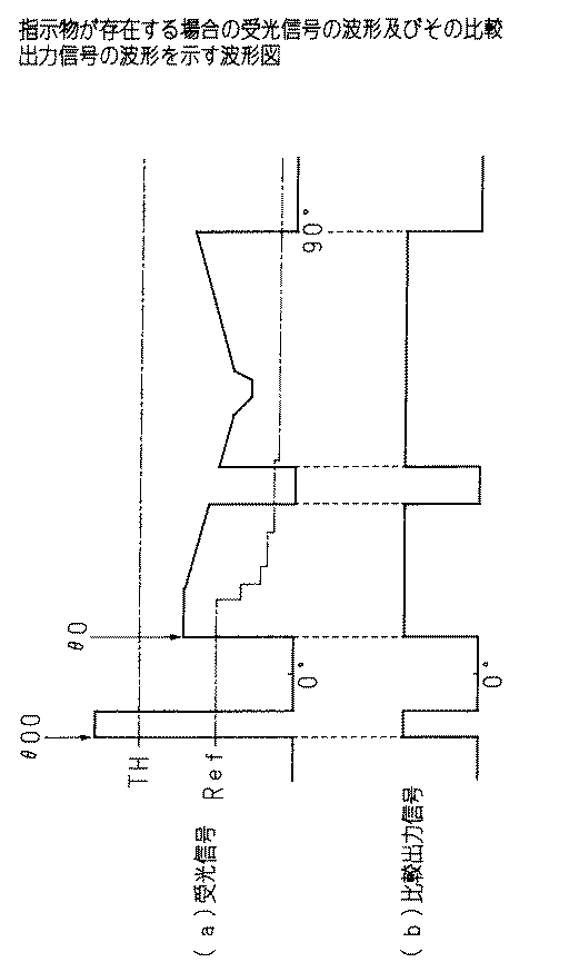
図7(a)に、指示物Sが存在する場合の受光素子13aによる受光信号の波形並びにコンパレータ33aにおけるしきい値Refの波形を示し、図7(b)に、そのときのコンパレータ33aによる比較出力信号の波形を示す。なお、光送受ユニット1bの場合もこれと同様である。
【0049】
表示画面10上の走査光の光路に指示物Sが存在する場合には、光送受ユニット1a,1bから投射された光の指示物Sからの反射光は受光素子13a,13bに入射されない。従って、図5に示されているような状態では,走査角度が0°からθ0までの間では受光素子13aには反射光は入射されず、走査角度がθ0からθ1までの間では受光素子13aに反射光が入射され、走査角度がθ1からθ2までの間では受光素子13aに反射光が入射されない。同様に、走査角度が0°からφ0までの間では受光素子13bには反射光は入射されず、走査角度がφ0からφ1までの間では受光素子13bに反射光が入射され、走査角度がφ1からφ2までの間では受光素子13bに反射光が入射されない。
【0050】
このような角度は、図7(a),(b)に示すような受光信号のレベルとしきい値Refとの比較結果、言い換えると受光信号の立ち上がりまたは立ち下がりのタイミングから求められる(図8(a),(b)参照)。従って、指示物Sとしての人の指による遮断範囲を、dθ=θ2−θ1,dφ=φ2−φ1として求めることができる。
【0051】
なお、θ00及びφ00とθ0及びφ0とは、両光送受ユニット1a,1bを結ぶ基準線と受光素子13a,13bとの位置関係及び再帰性反射シート7の端部の位置関係から既知であることは言うまでもない。
【0052】
このように本発明の光走査型タッチパネルにあっては、光走査角度(光走査開始からの経過時間)に応じてコンパレータ33aのしきい値Refの大きさを変動させ、受光素子13a(13b)の出力をこのしきい値Refと比較することによって光走査の遮断範囲を得るようにしたので、受光素子13a(13b)への直接入射光の影響を除去して、正確な遮断範囲を求めることができる。
【0053】
次に、このようにして求めた遮断範囲から、指示物S(本例では指)の中心位置(指示位置)の座標を求める処理について説明する。まず、三角測量に基づく角度から直交座標への変換を説明する。図9に示すように、光送受ユニット1aの位置を原点O、表示画面10の右辺,上辺をX軸,Y軸に設定し、基準線の長さ(光送受ユニット1a,1b間の距離)をLとする。また、光送受ユニット1bの位置をBとする。表示画面10上の指示物Sが指示した中心点P(Px,Py)が、光送受ユニット1a,1bからX軸に対してθ,φの角度でそれぞれ位置している場合、点PのX座標Px,Y座標Pyの値は、三角測量の原理により、それぞれ以下の(1),(2)式のように求めることができる。
【0054】
Px=(tanφ)÷(tanθ+tanφ)×L …(1)
Py=(tanθ・tanφ)÷(tanθ+tanφ)×L …(2)
【0055】
ところで、指示物S(指)には大きさがあるので、検出した受光信号の立ち上がり/立ち下がりのタイミングでの検出角度を採用した場合、図10に示すように、指示物S(指)のエッジ部の4点(図10のP1〜P4)を検出することになる。これらの4点は何れも指示した中心点(図10のPc)とは異なっている。そこで、以下のようにして 中心点Pcの座標(Pcx,Pcy)を求める。Px=Px(θ,φ),Py=Py(θ,φ)とした場合に、Pcx,Pcyは、それぞれ以下の(3),(4)式のように表せる。
【0056】
Pcx=Pcx(θ1+dθ/2,φ1+dφ/2) …(3)
Pcy=Pcy(θ1+dθ/2,φ1+dφ/2) …(4)
【0057】
そこで、(3),(4)式で表されるθ1+dθ/2,φ1+dφ/2を上記(1),(2)式のθ,φとして代入することにより、指示された中心点Pcの座標を求めることができる。
【0058】
なお、上述した例では、最初に角度の平均値を求め、その角度の平均値を三角測量の変換式(1),(2)に代入して、指示位置である中心点Pcの座標を求めるようにしたが、最初に三角測量の変換式(1),(2)に従って走査角度から4点P1〜P4の直交座標を求め、求めた4点の座標値の平均を算出して、中心点Pcの座標を求めるようにすることも可能である。また、視差、及び、指示位置の見易さを考慮して、指示位置である中心点Pcの座標を決定することも可能である。
【0059】
ところで、前述したように、ポリゴンミラー16a,16bの回転角速度が一定であるので、時間を計時することにより走査角度の情報を得ることができる。図11は、受光信号検出回路3aからの受光信号と、ポリゴンミラー16aの走査角度θ及び走査時間Tとの関係を示すタイミングチャートである。ポリゴンミラー16aの走査角速度が一定である場合、その走査角速度をωとすると、走査角度θ及び走査時間Tには、下記(5)式に示すような比例関係が成り立つ。
θ=ω×T …(5)
【0060】
よって、受光信号の立ち下がり,立ち上がり時の角度θ1,θ2は、それぞれの走査時間t1,t2と下記(6),(7)式の関係が成り立つ。
θ1=ω×t1 …(6)
θ2=ω×t2 …(7)
【0061】
従って、ポリゴンミラー16a,16bの走査角速度が一定である場合には、時間情報を用いて、指示物S(指)の遮断範囲及び座標位置を計測することが可能である。
【0062】
また、本発明の光走査型タッチパネルでは、計測した遮断範囲から指示物S(指)の大きさ(断面長)を求めることも可能である。図12は、この断面長計測の原理を示す模式図である。図12において、D1,D2はそれぞれ光送受ユニット1a,1bから見た指示物Sの断面長である。まず、光送受ユニット1a,1bの位置O(0,0),B(L,0)から指示物Sの中心点Pc(Pcx,Pcy)までの距離OPc(r1),BPc(r2)が、下記(8),(9)式の如く求められる。
【0063】
OPc=r1=(Pcx2 +Pcy2 )1/2 …(8)
BPc=r2={(L−Pcx)2 +Pcy2 }1/2 …(9)
【0064】
断面長は距離と遮断角度の正弦値との積で近似できるので、各断面長D1,D2は、下記(10),(11)式に従って計測可能である。
【0065】
なお、θ,φ≒0である場合には、sindθ≒dθ≒tandθ,sindφ≒dφ≒tandφと近似できるので、(10),(11)式においてsindθ,sindφの代わりに、dθまたはtandθ,dφまたはtandφとしても良い。
【0067】
【発明の効果】
以上のように、本発明の光走査型タッチパネルでは、指示物による遮断範囲であるか否かを判断する際の基準となるしきい値を、走査角度に応じて変更するようにしたので、受光素子への直接入射光の影響を除去して、正確な遮断範囲を求めることができ、その結果、指示物の位置,大きさの精度が高い算出結果を得ることができる。
【図面の簡単な説明】
【図1】本発明の光走査型タッチパネルの基本構成を示す模式図である。
【図2】光送受ユニットの内部構成及び光路を示す模式図である。
【図3】本発明の光走査型タッチパネルのブロック図である。
【図4】受光信号検出回路の構成例を示すブロック図である。
【図5】本発明の光走査型タッチパネルの実施状態を示す模式図である。
【図6】指示物が存在しない場合の受光信号の波形及びその比較出力信号の波形を示す波形図である。
【図7】指示物が存在する場合の受光信号の波形及びその比較出力信号の波形を示す波形図である。
【図8】受光信号のレベル変化を示すタイミングチャートである。
【図9】座標検出のための三角測量の原理を示す模式図である。
【図10】指示物及び遮断範囲を示す模式図である。
【図11】受光信号と走査角度と走査時間との関係を示すタイミングチャートである。
【図12】断面長計測の原理を示す模式図である。
【符号の説明】
1a,1b 光送受ユニット
2a,2b 発光素子駆動回路
3a,3b 受光信号検出回路
5 MPU
7 再帰性反射シート
10 表示画面(座標面)
11a,11b 発光素子
13a,13b 受光素子
16a,16b ポリゴンミラー
25 ROM
26 RAM
33a(33b),38a(38b) コンパレータ
34a(34b) 第1タイマ
39a(39b) 第2タイマ[0001]
BACKGROUND OF THE INVENTION
The present invention relates to an optical scanning touch panel that optically detects the position and size of an indicator on a display screen of a display device on which information is displayed by a computer system or the like.
[0002]
[Prior art]
With the spread of computer systems such as personal computers mainly, new information can be input by instructing on the display screen of a display device on which information is displayed by the computer system with a human finger or a specific indicator, Devices that give various instructions to a computer system are used.
[0003]
When an input operation is performed on the information displayed on the display screen of a display device such as a personal computer by a touch method, the contact position (indicated position) on the display screen is detected with high accuracy. There is a need. As a method for detecting the indicated position on the display screen serving as such a coordinate plane, a “carol method” (US Pat. No. 4,267,443) is known. In this method, a light matrix is formed on the front surface of the display screen by arranging a light emitting element and a light receiving element facing each other on the front frame of the display screen, and a light blocking position due to a finger or pen contact is detected. . In this method, it is possible to obtain a high S / N and to expand the application to a large display device, but the detection resolution is proportional to the arrangement interval of the light emitting element and the light receiving element, so that the detection resolution is increased. Therefore, it is necessary to narrow the arrangement interval. Therefore, in order to detect the contact position with high accuracy even when a small object such as a pen tip is contacted to the large screen, the number of light emitting elements and light receiving elements to be arranged increases, and the configuration is large. There is a problem that the signal processing becomes complicated as well as bulky.
[0004]
Another optical position detection method is disclosed in JP-A-57-211637. In this method, a focused light such as a laser beam is angle-scanned from the outside of the display screen, the angles at which the dedicated pen exists are determined from two timings of the reflected light from the dedicated pen having the reflecting means, and the obtained angles Is applied to the principle of triangulation and position coordinates are detected by calculation. In this method, the number of parts can be greatly reduced, and high resolution can be achieved. However, there is a problem in operability such as the use of a dedicated reflective pen, and the position of a finger, an arbitrary pen, etc. cannot be detected.
[0005]
Still another optical position detection method is proposed in Japanese Patent Laid-Open No. 62-5428. In this method, optical retroreflectors are arranged on both side frames of the display screen, the return light from the optical retroreflector of the angle-scanned laser beam is detected, and from the timing when the light beam is blocked by a finger or a pen. The presence angle of the finger or pen is obtained, and the position coordinates are detected from the obtained angle by the principle of triangulation. In this method, the number of parts is small and detection accuracy can be maintained, and the position of a finger, an arbitrary pen, or the like can be detected.
[0006]
In addition, an optical detection method that detects not only the position of a finger, an arbitrary pen, etc. but also its size is proposed in Japanese Patent Application No. 9-254220 by the same applicant as the present invention. In this method, at least two optical transmission / reception units that angularly scan laser light in a plane substantially parallel to the display screen are arranged at the corners of the display screen, and the optical retroreflector is disposed along at least three sides of the display screen. Measures the scanning light blocking range by an indicator such as a finger or pen in the scanning plane, calculates the position of the indicator in the scanning plane according to the triangulation principle, and calculates the size of the indicator To do.
[0007]
[Problems to be solved by the invention]
In the above-described three conventional examples in which light is angularly scanned, the light emitting element and the light receiving element that receives reflected light are close to each other in order to reduce the size of the optical transmission / reception unit, and the scanning angle is small. When optical scanning is performed, there is a possibility that part of the skirt of the emitted laser light from the light emitting element is directly incident on the light receiving element. When laser light is directly incident on the light receiving element from the light emitting element, the output level of the light receiving element fluctuates, and the direct incident light is mistaken for reflected light, so that the scanning light blocking range can be accurately measured. As a result, there is a problem that the correct position or size of the indicator cannot be calculated.
[0008]
The present invention has been made in view of such circumstances, and by switching the threshold value for the output of the light receiving element for determining whether or not it is in the cutoff range to a plurality of stages according to the scanning angle, scanning is performed. It is an object of the present invention to provide an optical scanning touch panel that can accurately measure the light blocking range and, as a result, can calculate the correct position or size of the indicator.
[0009]
[Means for Solving the Problems]
An optical scanning touch panel according to
[0010]
An optical scanning touch panel according to a second aspect of the present invention is the optical scanning touch panel according to the first aspect, wherein when the angle of the scanning light is small, a large reference value is selected, and when the angle of the scanning light is large, a small reference value is selected. It is characterized by that.
[0011]
An optical scanning touch panel according to a third aspect of the present invention is the optical scanning touch panel according to the first or second aspect, wherein the angle detection unit includes an optical scanning start detection unit that detects the start of optical scanning, and a timer that has a time measuring function. The angle of the scanning light is detected in accordance with the elapsed time measured by the timer from the time when the start of optical scanning is detected by the scanning start detection means.
[0012]
The optical scanning touch panel according to a fourth aspect of the present invention is the optical scanning touch panel according to the third aspect, wherein the optical scanning start detection means sets the timing at which the light receiving element starts receiving light of a predetermined level or more as the optical scanning start timing. Features.
[0013]
When the light receiving level of the light receiving element is larger than a predetermined threshold value, it is determined that the scanning light is reflected by the light retroreflective member and received by the light receiving element, and the range is the scanning light formed by the indicator. On the other hand, if the light receiving level of the light receiving element is smaller than a predetermined threshold value, it is determined that the scanning light has been blocked by the indicator, and the range of the scanning light formed by the indicator is determined. Measurement is performed as a blocking range, and the position and size of the indicator are calculated based on the measurement result. Here, in the optical scanning type touch panel according to the present invention, the threshold value that is a criterion for determining whether or not it is in the cutoff range is changed according to the scanning angle. In other words, the threshold value is set large at a small scanning angle at which a part of the scanning light may be directly incident, and the threshold value is set small at a large scanning angle other than that. In this way, since the threshold value is set in consideration of the direct incident light, it is possible to measure an accurate blocking range, and the position and size of the indicator calculated based on this blocking range are also included. An accurate value is obtained.
[0014]
If the rotational angular velocity of the polygon mirror in the optical scanning unit is constant, the scanning angle is proportional to the rotation time. Therefore, the scanning angle is detected based on the elapsed time from the start of scanning. It can be easily detected.
[0015]
DETAILED DESCRIPTION OF THE INVENTION
Hereinafter, the present invention will be described in detail with reference to the drawings showing embodiments thereof. FIG. 1 is a schematic diagram showing a basic configuration of an optical scanning touch panel according to the present invention.
[0016]
In FIG. 1,
[0017]
For example, one short side of the rectangular display screen 10 (the right side in this embodiment) that is a range of a plane defined as a target area to be touched by an indicator (blocker) S such as a finger or a pen. The light transmission / reception units 1a and 1b each having an optical system including a light emitting element, a light receiving element, a polygon mirror and the like are provided outside the two corners. Further, the
[0018]
Reference numeral 70 is a light shielding member. The light shielding member 70 is configured so that light is not directly incident between the light transmitting / receiving units 1a and 1b, specifically, the light projected from the light transmitting / receiving unit 1a is not incident on the light transmitting / receiving unit 1b, and vice versa. In order to prevent light projected from the light transmission / reception unit 1b from entering the light transmission / reception unit 1a, the light transmission / reception unit 1a is provided on a line connecting the light transmission / reception units 1a, 1b. The light shielding member 70 is an object having a practical light reflectance of “0”, and is configured to have a height approximately equal to the height of the
[0019]
FIG. 2 is a schematic diagram showing an internal configuration and optical paths of the optical transmission / reception units 1a and 1b. Both optical transmission / reception units 1a and 1b include light-emitting elements 11a and 11b made of laser diodes that emit infrared laser light,
[0020]
Angular scanning of light of 90 degrees or more is realized by rotation of the polygon mirrors 16a and 16b. The
[0021]
The laser beams emitted from the light emitting elements 11a and 11b are collimated by
[0022]
Each of the light transmitting / receiving units 1a and 1b includes light emitting
[0023]
In such an optical scanning touch panel of the present invention, as shown in FIG. 1, for example, the light transmission / reception unit 1b will be described. From the position where the projection light from the light transmission / reception unit 1b is incident on the light receiving element 13b. 1 is scanned in the counterclockwise direction in FIG. 1 after passing through the position shielded by the light shielding member 70, reaches the position (Ps) reflected by the tip portion of the
[0024]
However, in the light transmission / reception unit 1a, light is scanned clockwise in FIG. Here, the light transmission / reception unit 1a sets the lower side of the
[0025]
In the case of the optical transmission / reception unit 1b, either the upper side or the left side of the
[0026]
By the way, as shown in FIG. 1, the
[0027]
Due to the sawtooth portions 7a and 7b of the retroreflective sheet, for example, the projection light from the light transmitting / receiving unit 1b is scanned from the position Ps to the position P3 of one end of the sawtooth portion 7b of the retroreflective sheet. Since the incident angle to the
[0028]
FIG. 3 is a block diagram showing the relationship between the
[0029]
The
[0030]
Further, the
[0031]
FIG. 4 is a block diagram showing a configuration example of the light reception
[0032]
Since the
[0033]
Further, the output of the low-
[0034]
The operation of the light reception
[0035]
The
[0036]
Since the output of the
[0037]
The
[0038]
The comparator 33a compares the output of the
[0039]
Next, the calculation operation of the position and size of the pointing object S by the optical scanning touch panel of the present invention will be described. FIG. 5 is a schematic diagram showing an implementation state of the optical scanning touch panel. However, in FIG. 5, components other than the optical transmission / reception units 1a and 1b, the
[0040]
The
[0041]
In FIG. 5, θ00 and φ00 are angles from the reference line connecting the two light transmitting / receiving units 1a and 1b to the
[0042]
FIG. 6A shows the waveform of the light reception signal by the
[0043]
The
[0044]
When the polygon mirror 16a (16b) is a four-sided regular polygon as in the present embodiment, the polygon mirror 16a (16b) is rotated by a quarter in one cycle counted by the
[0045]
When the indicator S is not present in the optical path of the scanning light, retroreflective following the direct incidence on the
[0046]
In addition, the threshold value Ref is high at a small scanning angle (immediately after the start of optical scanning) in which a part of the laser light emitted from the light emitting element 11a (11b) is likely to be directly incident on the
[0047]
By the way, when the threshold value Ref is set in the comparator 33a as described above, the
[0048]
FIG. 7A shows the waveform of the light reception signal by the
[0049]
When the indicator S exists in the optical path of the scanning light on the
[0050]
Such an angle is obtained from the comparison result between the level of the received light signal and the threshold value Ref as shown in FIGS. 7A and 7B, in other words, from the rising or falling timing of the received light signal (FIG. 8 ( a), see (b)). Therefore, the blocking range by the finger of the person as the indicator S can be obtained as dθ = θ2−θ1 and dφ = φ2−φ1.
[0051]
Note that θ00 and φ00 and θ0 and φ0 are known from the positional relationship between the reference line connecting both the light transmitting and receiving units 1a and 1b and the
[0052]
As described above, in the optical scanning type touch panel of the present invention, the magnitude of the threshold value Ref of the comparator 33a is changed according to the optical scanning angle (elapsed time from the start of optical scanning), and the
[0053]
Next, processing for obtaining the coordinates of the center position (designated position) of the pointing object S (finger in this example) from the cut-off range obtained in this way will be described. First, the conversion from an angle based on triangulation to Cartesian coordinates will be described. As shown in FIG. 9, the position of the optical transmission / reception unit 1a is set to the origin O, the right side and the upper side of the
[0054]
Px = (tan φ) ÷ (tan θ + tan φ) × L (1)
Py = (tan θ · tan φ) ÷ (tan θ + tan φ) × L (2)
[0055]
By the way, since the indicator S (finger) has a size, when the detected angle at the rising / falling timing of the detected light reception signal is adopted, as shown in FIG. Four points (P1 to P4 in FIG. 10) of the edge portion are detected. These four points are all different from the designated center point (Pc in FIG. 10). Therefore, the coordinates (Pcx, Pcy) of the center point Pc are obtained as follows. When Px = Px (θ, φ) and Py = Py (θ, φ), Pcx and Pcy can be expressed by the following equations (3) and (4), respectively.
[0056]
Pcx = Pcx (θ1 + dθ / 2, φ1 + dφ / 2) (3)
Pcy = Pcy (θ1 + dθ / 2, φ1 + dφ / 2) (4)
[0057]
Therefore, by substituting θ1 + dθ / 2 and φ1 + dφ / 2 represented by the equations (3) and (4) as θ and φ in the above equations (1) and (2), the coordinates of the instructed center point Pc are obtained. Can be sought.
[0058]
In the above-described example, the average value of the angle is first obtained, and the average value of the angle is substituted into the triangulation conversion formulas (1) and (2) to obtain the coordinates of the center point Pc that is the designated position. First, the orthogonal coordinates of the four points P1 to P4 are obtained from the scanning angle according to the triangulation conversion formulas (1) and (2), the average of the obtained coordinate values of the four points is calculated, and the center point It is also possible to obtain the coordinates of Pc. Further, it is possible to determine the coordinates of the center point Pc that is the designated position in consideration of the parallax and the visibility of the designated position.
[0059]
Incidentally, as described above, since the rotational angular velocities of the polygon mirrors 16a and 16b are constant, the information of the scanning angle can be obtained by measuring the time. FIG. 11 is a timing chart showing the relationship between the light reception signal from the light reception
θ = ω × T (5)
[0060]
Therefore, the angles θ1 and θ2 at the time of falling and rising of the received light signal have the relationship between the scanning times t1 and t2 and the following expressions (6) and (7).
θ1 = ω × t1 (6)
θ2 = ω × t2 (7)
[0061]
Therefore, when the scanning angular velocities of the polygon mirrors 16a and 16b are constant, it is possible to measure the blocking range and coordinate position of the indicator S (finger) using the time information.
[0062]
In the optical scanning touch panel of the present invention, the size (cross-sectional length) of the indicator S (finger) can be obtained from the measured blocking range. FIG. 12 is a schematic diagram showing the principle of the cross-sectional length measurement. In FIG. 12, D1 and D2 are cross-sectional lengths of the indicator S as viewed from the optical transmission / reception units 1a and 1b, respectively. First, the distances OPc (r1) and BPc (r2) from the positions O (0, 0) and B (L, 0) of the optical transmission / reception units 1a and 1b to the center point Pc (Pcx, Pcy) of the indicator S are It is obtained as shown in the following equations (8) and (9).
[0063]
OPc = r1 = (Pcx 2 + Pcy 2 ) 1/2 (8)
BPc = r2 = {(L-Pcx) 2 + Pcy 2 } 1/2 (9)
[0064]
Since the cross-sectional length can be approximated by the product of the distance and the sine value of the cutoff angle, the cross-sectional lengths D1 and D2 can be measured according to the following equations (10) and (11).
[0065]
In the case of θ, φ≈0, it can be approximated as sinθ≈dθ≈tandθ, sindφ≈dφ≈tandφ. Therefore, in the equations (10) and (11), dθ or tandθ, dφ instead of sindθ and sindφ. Alternatively, tandφ may be used.
[0067]
【The invention's effect】
As described above, in the optical scanning touch panel according to the present invention, the threshold value used as a reference for determining whether or not the range is the blocking range by the indicator is changed according to the scanning angle. By removing the influence of the direct incident light on the element, an accurate blocking range can be obtained, and as a result, a calculation result with high accuracy of the position and size of the indicator can be obtained.
[Brief description of the drawings]
FIG. 1 is a schematic diagram showing a basic configuration of an optical scanning touch panel of the present invention.
FIG. 2 is a schematic diagram showing an internal configuration and an optical path of an optical transmission / reception unit.
FIG. 3 is a block diagram of an optical scanning touch panel according to the present invention.
FIG. 4 is a block diagram illustrating a configuration example of a light reception signal detection circuit.
FIG. 5 is a schematic view showing an implementation state of the optical scanning touch panel of the present invention.
FIG. 6 is a waveform diagram showing a waveform of a received light signal and a waveform of a comparison output signal when there is no indicator.
FIG. 7 is a waveform diagram showing a waveform of a received light signal and a waveform of a comparison output signal when an indicator is present.
FIG. 8 is a timing chart showing a change in level of a received light signal.
FIG. 9 is a schematic diagram showing the principle of triangulation for coordinate detection.
FIG. 10 is a schematic diagram showing an indicator and a blocking range.
FIG. 11 is a timing chart showing a relationship among a light reception signal, a scanning angle, and a scanning time.
FIG. 12 is a schematic diagram showing the principle of cross-sectional length measurement.
[Explanation of symbols]
1a, 1b Light transmission /
7
11a, 11b
26 RAM
33a (33b), 38a (38b) Comparator 34a (34b)
Claims (4)
Priority Applications (5)
| Application Number | Priority Date | Filing Date | Title |
|---|---|---|---|
| JP23206898A JP3827450B2 (en) | 1998-08-18 | 1998-08-18 | Optical scanning touch panel |
| PCT/JP1999/002930 WO2000011542A1 (en) | 1998-08-18 | 1999-06-01 | Scanning-light touch panel |
| DE69937253T DE69937253T2 (en) | 1998-08-18 | 1999-06-01 | LIGHT SCANNER TOUCH SENSITIVE SCREEN |
| EP99922636A EP1139207B1 (en) | 1998-08-18 | 1999-06-01 | Scanning-light touch panel |
| US09/761,752 US6492633B2 (en) | 1998-08-18 | 2001-01-18 | Optical scanning-type touch panel |
Applications Claiming Priority (1)
| Application Number | Priority Date | Filing Date | Title |
|---|---|---|---|
| JP23206898A JP3827450B2 (en) | 1998-08-18 | 1998-08-18 | Optical scanning touch panel |
Publications (2)
| Publication Number | Publication Date |
|---|---|
| JP2000066825A JP2000066825A (en) | 2000-03-03 |
| JP3827450B2 true JP3827450B2 (en) | 2006-09-27 |
Family
ID=16933492
Family Applications (1)
| Application Number | Title | Priority Date | Filing Date |
|---|---|---|---|
| JP23206898A Expired - Fee Related JP3827450B2 (en) | 1998-08-18 | 1998-08-18 | Optical scanning touch panel |
Country Status (5)
| Country | Link |
|---|---|
| US (1) | US6492633B2 (en) |
| EP (1) | EP1139207B1 (en) |
| JP (1) | JP3827450B2 (en) |
| DE (1) | DE69937253T2 (en) |
| WO (1) | WO2000011542A1 (en) |
Families Citing this family (91)
| Publication number | Priority date | Publication date | Assignee | Title |
|---|---|---|---|---|
| JP2000311048A (en) * | 1999-04-27 | 2000-11-07 | Matsushita Electric Ind Co Ltd | Operation device |
| JP4094794B2 (en) * | 1999-09-10 | 2008-06-04 | 株式会社リコー | Coordinate detection apparatus, information storage medium, and coordinate detection method |
| DE10085378B3 (en) * | 2000-02-02 | 2013-09-26 | Fujitsu Limited | Optical position detection device |
| JP4393030B2 (en) * | 2000-04-14 | 2010-01-06 | 富士通株式会社 | Optical position detection device and recording medium |
| JP2002268810A (en) * | 2001-03-13 | 2002-09-20 | Canon Inc | Coordinate input device |
| US6724366B2 (en) * | 2001-04-03 | 2004-04-20 | Peter James Crawford | Thumb actuated x-y input device |
| US8674966B2 (en) | 2001-11-02 | 2014-03-18 | Neonode Inc. | ASIC controller for light-based touch screen |
| US9052777B2 (en) | 2001-11-02 | 2015-06-09 | Neonode Inc. | Optical elements with alternating reflective lens facets |
| US9052771B2 (en) * | 2002-11-04 | 2015-06-09 | Neonode Inc. | Touch screen calibration and update methods |
| US9164654B2 (en) * | 2002-12-10 | 2015-10-20 | Neonode Inc. | User interface for mobile computer unit |
| US9471170B2 (en) * | 2002-11-04 | 2016-10-18 | Neonode Inc. | Light-based touch screen with shift-aligned emitter and receiver lenses |
| US8095879B2 (en) * | 2002-12-10 | 2012-01-10 | Neonode Inc. | User interface for mobile handheld computer unit |
| US8896575B2 (en) * | 2002-11-04 | 2014-11-25 | Neonode Inc. | Pressure-sensitive touch screen |
| US8416217B1 (en) | 2002-11-04 | 2013-04-09 | Neonode Inc. | Light-based finger gesture user interface |
| US8587562B2 (en) * | 2002-11-04 | 2013-11-19 | Neonode Inc. | Light-based touch screen using elliptical and parabolic reflectors |
| US6954197B2 (en) * | 2002-11-15 | 2005-10-11 | Smart Technologies Inc. | Size/scale and orientation determination of a pointer in a camera-based touch system |
| US8902196B2 (en) * | 2002-12-10 | 2014-12-02 | Neonode Inc. | Methods for determining a touch location on a touch screen |
| US8403203B2 (en) * | 2002-12-10 | 2013-03-26 | Neonoda Inc. | Component bonding using a capillary effect |
| US9389730B2 (en) * | 2002-12-10 | 2016-07-12 | Neonode Inc. | Light-based touch screen using elongated light guides |
| US9195344B2 (en) * | 2002-12-10 | 2015-11-24 | Neonode Inc. | Optical surface using a reflected image for determining three-dimensional position information |
| US7133032B2 (en) * | 2003-04-24 | 2006-11-07 | Eastman Kodak Company | OLED display and touch screen |
| JP4185825B2 (en) * | 2003-07-01 | 2008-11-26 | キヤノン株式会社 | Coordinate input device, control method therefor, information processing device, and program |
| KR100601957B1 (en) * | 2004-07-07 | 2006-07-14 | 삼성전자주식회사 | Method and device for determining image correspondence for face recognition, Image correction method and device for achieving this |
| JP4515881B2 (en) * | 2004-10-19 | 2010-08-04 | パイオニア株式会社 | Coordinate position detection apparatus and detection method |
| CA2588806A1 (en) * | 2004-12-09 | 2006-06-15 | Rpo Pty Limited | Optical power distribution devices |
| US7503658B2 (en) | 2005-01-20 | 2009-03-17 | Hewlett-Packard Development Company, L.P. | Projector |
| JP4612853B2 (en) * | 2005-03-29 | 2011-01-12 | キヤノン株式会社 | Pointed position recognition device and information input device having the same |
| JP4687882B2 (en) * | 2005-07-29 | 2011-05-25 | スタンレー電気株式会社 | Capacitive lock switch |
| JP4750650B2 (en) * | 2006-08-22 | 2011-08-17 | リコーエレメックス株式会社 | Drawing display device, drawing display method and program |
| WO2008066004A1 (en) * | 2006-11-30 | 2008-06-05 | Sega Corporation | Position inputting apparatus |
| US8716614B2 (en) * | 2007-10-10 | 2014-05-06 | Flatfrog Laboratories Ab | Touch pad and a method of operating the touch pad |
| CN101546235B (en) * | 2008-03-28 | 2011-07-27 | 旭丽电子(广州)有限公司 | Touch panel module and method for determining voltage contact position on touch panel |
| TW201001258A (en) * | 2008-06-23 | 2010-01-01 | Flatfrog Lab Ab | Determining the location of one or more objects on a touch surface |
| TW201007530A (en) | 2008-06-23 | 2010-02-16 | Flatfrog Lab Ab | Detecting the location of an object on a touch surface |
| TW201005606A (en) * | 2008-06-23 | 2010-02-01 | Flatfrog Lab Ab | Detecting the locations of a plurality of objects on a touch surface |
| TW201013492A (en) * | 2008-06-23 | 2010-04-01 | Flatfrog Lab Ab | Determining the location of one or more objects on a touch surface |
| US8542217B2 (en) * | 2008-06-23 | 2013-09-24 | Flatfrog Laboratories Ab | Optical touch detection using input and output beam scanners |
| TWI398803B (en) * | 2008-11-28 | 2013-06-11 | Hon Hai Prec Ind Co Ltd | Electronic device with infrared touch function and control method thereof |
| SE533704C2 (en) | 2008-12-05 | 2010-12-07 | Flatfrog Lab Ab | Touch sensitive apparatus and method for operating the same |
| US20100170725A1 (en) * | 2009-01-06 | 2010-07-08 | Hong Kong Applied Science And Technology Research Institute | Touch surface and system and method of detecting touch input |
| KR100913758B1 (en) * | 2009-02-09 | 2009-08-24 | 호감테크놀로지(주) | Touch position detection device of touch panel |
| TWI393037B (en) * | 2009-02-10 | 2013-04-11 | Quanta Comp Inc | Optical touch displaying device and operating method thereof |
| US20100207909A1 (en) * | 2009-02-13 | 2010-08-19 | Ming-Cho Wu | Detection module and an optical detection device comprising the same |
| US8775023B2 (en) | 2009-02-15 | 2014-07-08 | Neanode Inc. | Light-based touch controls on a steering wheel and dashboard |
| US9063614B2 (en) | 2009-02-15 | 2015-06-23 | Neonode Inc. | Optical touch screens |
| TW201032090A (en) * | 2009-02-16 | 2010-09-01 | Chih-Hsiung Lin | Laser scanning input device |
| US20100245264A1 (en) * | 2009-03-31 | 2010-09-30 | Arima Lasers Corp. | Optical Detection Apparatus and Method |
| KR101697133B1 (en) * | 2009-09-30 | 2017-02-01 | 베이징 아이어터치 시스템 코퍼레이션 리미티드 | Touch screen, touch system and method for positioning a touch object in a touch system |
| TWI398840B (en) * | 2009-10-12 | 2013-06-11 | Au Optronics Corp | Organic light emitting display having a power saving mechanism |
| AU2010308596A1 (en) * | 2009-10-19 | 2012-06-07 | Flatfrog Laboratories Ab | Determining touch data for one or more objects on a touch surface |
| KR101097992B1 (en) * | 2009-11-05 | 2011-12-26 | 주식회사 스마트센스테크놀러지 | Position recognition device of indicator |
| US20110128218A1 (en) * | 2009-12-01 | 2011-06-02 | Smart Technologies Ulc | Interactive input system and bezel therefor |
| KR20120067064A (en) * | 2010-12-15 | 2012-06-25 | 삼성전기주식회사 | Apparatus for detecting coordinates, display device, security device and electronic blackboard including the same |
| TW201235909A (en) * | 2011-02-24 | 2012-09-01 | Ind Tech Res Inst | Optical scanning-type touch apparatus and the operation method |
| CN103703340B (en) * | 2011-02-28 | 2017-12-19 | 百安托国际有限公司 | Systems and methods for sensing and tracking radiation blocking objects on surfaces |
| KR101221676B1 (en) * | 2011-05-20 | 2013-01-14 | 주식회사 에이에프오 | Infrared touch screen devices capable of multi-touch sensing |
| US8890848B2 (en) * | 2011-06-02 | 2014-11-18 | Uc-Logic Technology Corp. | Optical touch device |
| US9063616B2 (en) | 2011-06-02 | 2015-06-23 | Uc-Logic Technology Corp. | Optical touch device with symmetric light sources and locating method thereof |
| CN103425251B (en) * | 2012-05-22 | 2017-08-18 | 富泰华工业(深圳)有限公司 | Keyboard and input method |
| US10168835B2 (en) | 2012-05-23 | 2019-01-01 | Flatfrog Laboratories Ab | Spatial resolution in touch displays |
| US9164625B2 (en) | 2012-10-14 | 2015-10-20 | Neonode Inc. | Proximity sensor for determining two-dimensional coordinates of a proximal object |
| US9921661B2 (en) | 2012-10-14 | 2018-03-20 | Neonode Inc. | Optical proximity sensor and associated user interface |
| US10282034B2 (en) | 2012-10-14 | 2019-05-07 | Neonode Inc. | Touch sensitive curved and flexible displays |
| US9207800B1 (en) | 2014-09-23 | 2015-12-08 | Neonode Inc. | Integrated light guide and touch screen frame and multi-touch determination method |
| WO2014168567A1 (en) | 2013-04-11 | 2014-10-16 | Flatfrog Laboratories Ab | Tomographic processing for touch detection |
| TWI507947B (en) * | 2013-07-12 | 2015-11-11 | Wistron Corp | Apparatus and system for correcting touch signal and method thereof |
| WO2015005847A1 (en) | 2013-07-12 | 2015-01-15 | Flatfrog Laboratories Ab | Partial detect mode |
| JP2015088050A (en) * | 2013-10-31 | 2015-05-07 | 船井電機株式会社 | Projector device |
| US10126882B2 (en) | 2014-01-16 | 2018-11-13 | Flatfrog Laboratories Ab | TIR-based optical touch systems of projection-type |
| WO2015108479A1 (en) | 2014-01-16 | 2015-07-23 | Flatfrog Laboratories Ab | Light coupling in tir-based optical touch systems |
| WO2015199602A1 (en) | 2014-06-27 | 2015-12-30 | Flatfrog Laboratories Ab | Detection of surface contamination |
| WO2016122385A1 (en) | 2015-01-28 | 2016-08-04 | Flatfrog Laboratories Ab | Dynamic touch quarantine frames |
| US10318074B2 (en) | 2015-01-30 | 2019-06-11 | Flatfrog Laboratories Ab | Touch-sensing OLED display with tilted emitters |
| EP3537269A1 (en) | 2015-02-09 | 2019-09-11 | FlatFrog Laboratories AB | Optical touch system |
| WO2016140612A1 (en) | 2015-03-02 | 2016-09-09 | Flatfrog Laboratories Ab | Optical component for light coupling |
| TWI612445B (en) * | 2015-09-21 | 2018-01-21 | 緯創資通股份有限公司 | Optical touch apparatus and a method for determining a touch position |
| KR102400705B1 (en) | 2015-12-09 | 2022-05-23 | 플라트프로그 라보라토리즈 에이비 | Improved stylus identification |
| CN110100226A (en) | 2016-11-24 | 2019-08-06 | 平蛙实验室股份公司 | The Automatic Optimal of touch signal |
| CN119847372A (en) | 2016-12-07 | 2025-04-18 | 平蛙实验室股份公司 | Touch sensing device |
| CN116679845A (en) | 2017-02-06 | 2023-09-01 | 平蛙实验室股份公司 | touch sensing device |
| US20180275830A1 (en) | 2017-03-22 | 2018-09-27 | Flatfrog Laboratories Ab | Object characterisation for touch displays |
| WO2018182476A1 (en) | 2017-03-28 | 2018-10-04 | Flatfrog Laboratories Ab | Touch sensing apparatus and method for assembly |
| CN117311543A (en) | 2017-09-01 | 2023-12-29 | 平蛙实验室股份公司 | Touch sensing device |
| WO2019172826A1 (en) | 2018-03-05 | 2019-09-12 | Flatfrog Laboratories Ab | Improved touch-sensing apparatus |
| CN112889016A (en) | 2018-10-20 | 2021-06-01 | 平蛙实验室股份公司 | Frame for touch sensitive device and tool therefor |
| WO2020153890A1 (en) | 2019-01-25 | 2020-07-30 | Flatfrog Laboratories Ab | A videoconferencing terminal and method of operating the same |
| EP4066089B1 (en) | 2019-11-25 | 2024-09-25 | FlatFrog Laboratories AB | A touch-sensing apparatus |
| CN115039060A (en) | 2019-12-31 | 2022-09-09 | 内奥诺德公司 | Non-contact touch input system |
| US12282653B2 (en) | 2020-02-08 | 2025-04-22 | Flatfrog Laboratories Ab | Touch apparatus with low latency interactions |
| US11893189B2 (en) | 2020-02-10 | 2024-02-06 | Flatfrog Laboratories Ab | Touch-sensing apparatus |
| EP4222586A4 (en) | 2020-09-30 | 2024-11-06 | Neonode Inc. | OPTICAL TOUCH SENSOR |
Family Cites Families (11)
| Publication number | Priority date | Publication date | Assignee | Title |
|---|---|---|---|---|
| US4267443A (en) | 1978-04-24 | 1981-05-12 | Carroll Manufacturing Corporation | Photoelectric input apparatus |
| US4294543A (en) * | 1979-11-13 | 1981-10-13 | Command Control & Communications Corporation | Optical system for developing point coordinate information |
| JPS5936295B2 (en) | 1981-06-23 | 1984-09-03 | 株式会社日立国際電気 | Optical coordinate input device |
| US4558313A (en) * | 1981-12-31 | 1985-12-10 | International Business Machines Corporation | Indicator to data processing interface |
| SE8602233L (en) * | 1985-06-05 | 1986-12-06 | Illinois Tool Works | OPTICAL DETERMINATION DEVICE |
| US4762990A (en) * | 1985-10-21 | 1988-08-09 | International Business Machines Corporation | Data processing input interface determining position of object |
| US4642422A (en) * | 1985-12-16 | 1987-02-10 | International Business Machines Corporation | Calibration of a scanning light interrupt type of data input interface |
| US4811004A (en) * | 1987-05-11 | 1989-03-07 | Dale Electronics, Inc. | Touch panel system and method for using same |
| US5525764A (en) * | 1994-06-09 | 1996-06-11 | Junkins; John L. | Laser scanning graphic input system |
| JPH09254220A (en) | 1996-03-21 | 1997-09-30 | Japan Steel Works Ltd:The | Injection control method for electric injection molding machine |
| JPH11110116A (en) | 1997-08-07 | 1999-04-23 | Fujitsu Ltd | Optical position detector |
-
1998
- 1998-08-18 JP JP23206898A patent/JP3827450B2/en not_active Expired - Fee Related
-
1999
- 1999-06-01 WO PCT/JP1999/002930 patent/WO2000011542A1/en not_active Ceased
- 1999-06-01 EP EP99922636A patent/EP1139207B1/en not_active Expired - Lifetime
- 1999-06-01 DE DE69937253T patent/DE69937253T2/en not_active Expired - Lifetime
-
2001
- 2001-01-18 US US09/761,752 patent/US6492633B2/en not_active Expired - Fee Related
Also Published As
| Publication number | Publication date |
|---|---|
| JP2000066825A (en) | 2000-03-03 |
| DE69937253T2 (en) | 2008-01-10 |
| US20010002694A1 (en) | 2001-06-07 |
| DE69937253D1 (en) | 2007-11-15 |
| US6492633B2 (en) | 2002-12-10 |
| WO2000011542A1 (en) | 2000-03-02 |
| EP1139207A1 (en) | 2001-10-04 |
| EP1139207B1 (en) | 2007-10-03 |
| EP1139207A4 (en) | 2006-04-19 |
Similar Documents
| Publication | Publication Date | Title |
|---|---|---|
| JP3827450B2 (en) | Optical scanning touch panel | |
| US6480187B1 (en) | Optical scanning-type touch panel | |
| JP4097353B2 (en) | Optical scanning touch panel | |
| JP4043128B2 (en) | Optical scanning touch panel | |
| US8115753B2 (en) | Touch screen system with hover and click input methods | |
| JP2001249762A (en) | Coordinate input / detection device, electronic blackboard system, position shift correction method of light receiving element, and storage medium | |
| US8791925B2 (en) | Coordinate input apparatus, control method therefor and program | |
| JPH11110116A (en) | Optical position detector | |
| JP4001585B2 (en) | Optical scanning touch panel | |
| JP3805316B2 (en) | Optical scanning touch panel | |
| JP3797803B2 (en) | Optical scanning touch panel | |
| JP4073069B2 (en) | Optical scanning touch panel | |
| JP3846981B2 (en) | Information display device with optical position detector | |
| JP4454667B2 (en) | Optical scanning touch panel | |
| JP3966592B2 (en) | Optical scanning touch panel | |
| JP4004177B2 (en) | Optical scanning touch panel | |
| JP6315127B2 (en) | Input device, aerial image interaction system, and input method | |
| JP2005173684A (en) | Optical coordinate input device | |
| JP2004185283A (en) | Optical coordinate input device | |
| WO2000014623A1 (en) | Optical scanning touch panel | |
| JP4175715B2 (en) | Optical scanning touch panel | |
| JP2016139213A (en) | Coordinate input device and control method thereof | |
| JP2001084108A (en) | Coordinate input / detection / display device | |
| JP2000132339A (en) | Coordinate input device | |
| JPWO2000014623A1 (en) | Optical scanning touch panel |
Legal Events
| Date | Code | Title | Description |
|---|---|---|---|
| A621 | Written request for application examination |
Free format text: JAPANESE INTERMEDIATE CODE: A621 Effective date: 20040818 |
|
| TRDD | Decision of grant or rejection written | ||
| A01 | Written decision to grant a patent or to grant a registration (utility model) |
Free format text: JAPANESE INTERMEDIATE CODE: A01 Effective date: 20060704 |
|
| A61 | First payment of annual fees (during grant procedure) |
Free format text: JAPANESE INTERMEDIATE CODE: A61 Effective date: 20060704 |
|
| R150 | Certificate of patent or registration of utility model |
Free format text: JAPANESE INTERMEDIATE CODE: R150 |
|
| FPAY | Renewal fee payment (event date is renewal date of database) |
Free format text: PAYMENT UNTIL: 20100714 Year of fee payment: 4 |
|
| FPAY | Renewal fee payment (event date is renewal date of database) |
Free format text: PAYMENT UNTIL: 20100714 Year of fee payment: 4 |
|
| FPAY | Renewal fee payment (event date is renewal date of database) |
Free format text: PAYMENT UNTIL: 20110714 Year of fee payment: 5 |
|
| FPAY | Renewal fee payment (event date is renewal date of database) |
Free format text: PAYMENT UNTIL: 20110714 Year of fee payment: 5 |
|
| FPAY | Renewal fee payment (event date is renewal date of database) |
Free format text: PAYMENT UNTIL: 20120714 Year of fee payment: 6 |
|
| FPAY | Renewal fee payment (event date is renewal date of database) |
Free format text: PAYMENT UNTIL: 20120714 Year of fee payment: 6 |
|
| FPAY | Renewal fee payment (event date is renewal date of database) |
Free format text: PAYMENT UNTIL: 20130714 Year of fee payment: 7 |
|
| LAPS | Cancellation because of no payment of annual fees |