JP3824657B2 - Data memory unit configured to store data within one clock cycle and method of operation thereof - Google Patents
Data memory unit configured to store data within one clock cycle and method of operation thereof Download PDFInfo
- Publication number
- JP3824657B2 JP3824657B2 JP50596398A JP50596398A JP3824657B2 JP 3824657 B2 JP3824657 B2 JP 3824657B2 JP 50596398 A JP50596398 A JP 50596398A JP 50596398 A JP50596398 A JP 50596398A JP 3824657 B2 JP3824657 B2 JP 3824657B2
- Authority
- JP
- Japan
- Prior art keywords
- store
- data
- load
- cache
- instruction
- Prior art date
- Legal status (The legal status is an assumption and is not a legal conclusion. Google has not performed a legal analysis and makes no representation as to the accuracy of the status listed.)
- Expired - Fee Related
Links
Images


Classifications
-
- G—PHYSICS
- G06—COMPUTING OR CALCULATING; COUNTING
- G06F—ELECTRIC DIGITAL DATA PROCESSING
- G06F12/00—Accessing, addressing or allocating within memory systems or architectures
- G06F12/02—Addressing or allocation; Relocation
- G06F12/08—Addressing or allocation; Relocation in hierarchically structured memory systems, e.g. virtual memory systems
- G06F12/12—Replacement control
- G06F12/121—Replacement control using replacement algorithms
- G06F12/126—Replacement control using replacement algorithms with special data handling, e.g. priority of data or instructions, handling errors or pinning
-
- G—PHYSICS
- G06—COMPUTING OR CALCULATING; COUNTING
- G06F—ELECTRIC DIGITAL DATA PROCESSING
- G06F9/00—Arrangements for program control, e.g. control units
- G06F9/06—Arrangements for program control, e.g. control units using stored programs, i.e. using an internal store of processing equipment to receive or retain programs
- G06F9/30—Arrangements for executing machine instructions, e.g. instruction decode
- G06F9/30003—Arrangements for executing specific machine instructions
- G06F9/3004—Arrangements for executing specific machine instructions to perform operations on memory
- G06F9/30043—LOAD or STORE instructions; Clear instruction
-
- G—PHYSICS
- G06—COMPUTING OR CALCULATING; COUNTING
- G06F—ELECTRIC DIGITAL DATA PROCESSING
- G06F9/00—Arrangements for program control, e.g. control units
- G06F9/06—Arrangements for program control, e.g. control units using stored programs, i.e. using an internal store of processing equipment to receive or retain programs
- G06F9/30—Arrangements for executing machine instructions, e.g. instruction decode
- G06F9/30003—Arrangements for executing specific machine instructions
- G06F9/30076—Arrangements for executing specific machine instructions to perform miscellaneous control operations, e.g. NOP
- G06F9/30087—Synchronisation or serialisation instructions
-
- G—PHYSICS
- G06—COMPUTING OR CALCULATING; COUNTING
- G06F—ELECTRIC DIGITAL DATA PROCESSING
- G06F9/00—Arrangements for program control, e.g. control units
- G06F9/06—Arrangements for program control, e.g. control units using stored programs, i.e. using an internal store of processing equipment to receive or retain programs
- G06F9/30—Arrangements for executing machine instructions, e.g. instruction decode
- G06F9/38—Concurrent instruction execution, e.g. pipeline or look ahead
- G06F9/3818—Decoding for concurrent execution
- G06F9/382—Pipelined decoding, e.g. using predecoding
-
- G—PHYSICS
- G06—COMPUTING OR CALCULATING; COUNTING
- G06F—ELECTRIC DIGITAL DATA PROCESSING
- G06F9/00—Arrangements for program control, e.g. control units
- G06F9/06—Arrangements for program control, e.g. control units using stored programs, i.e. using an internal store of processing equipment to receive or retain programs
- G06F9/30—Arrangements for executing machine instructions, e.g. instruction decode
- G06F9/38—Concurrent instruction execution, e.g. pipeline or look ahead
- G06F9/3824—Operand accessing
-
- G—PHYSICS
- G06—COMPUTING OR CALCULATING; COUNTING
- G06F—ELECTRIC DIGITAL DATA PROCESSING
- G06F9/00—Arrangements for program control, e.g. control units
- G06F9/06—Arrangements for program control, e.g. control units using stored programs, i.e. using an internal store of processing equipment to receive or retain programs
- G06F9/30—Arrangements for executing machine instructions, e.g. instruction decode
- G06F9/38—Concurrent instruction execution, e.g. pipeline or look ahead
- G06F9/3836—Instruction issuing, e.g. dynamic instruction scheduling or out of order instruction execution
- G06F9/3838—Dependency mechanisms, e.g. register scoreboarding
- G06F9/384—Register renaming
-
- G—PHYSICS
- G06—COMPUTING OR CALCULATING; COUNTING
- G06F—ELECTRIC DIGITAL DATA PROCESSING
- G06F9/00—Arrangements for program control, e.g. control units
- G06F9/06—Arrangements for program control, e.g. control units using stored programs, i.e. using an internal store of processing equipment to receive or retain programs
- G06F9/30—Arrangements for executing machine instructions, e.g. instruction decode
- G06F9/38—Concurrent instruction execution, e.g. pipeline or look ahead
- G06F9/3854—Instruction completion, e.g. retiring, committing or graduating
- G06F9/3856—Reordering of instructions, e.g. using queues or age tags
-
- G—PHYSICS
- G06—COMPUTING OR CALCULATING; COUNTING
- G06F—ELECTRIC DIGITAL DATA PROCESSING
- G06F9/00—Arrangements for program control, e.g. control units
- G06F9/06—Arrangements for program control, e.g. control units using stored programs, i.e. using an internal store of processing equipment to receive or retain programs
- G06F9/30—Arrangements for executing machine instructions, e.g. instruction decode
- G06F9/38—Concurrent instruction execution, e.g. pipeline or look ahead
- G06F9/3854—Instruction completion, e.g. retiring, committing or graduating
- G06F9/3858—Result writeback, i.e. updating the architectural state or memory
Landscapes
- Engineering & Computer Science (AREA)
- Theoretical Computer Science (AREA)
- Software Systems (AREA)
- Physics & Mathematics (AREA)
- General Engineering & Computer Science (AREA)
- General Physics & Mathematics (AREA)
- Advance Control (AREA)
- Memory System Of A Hierarchy Structure (AREA)
- Executing Machine-Instructions (AREA)
Description
発明の背景
1.発明の分野
本発明は、スーパースカラマイクロプロセッサの分野に関し、より特定的には、スーパースカラマイクロプロセッサ内のロード/ストアユニットおよびデータキャッシュに関する。
2.関連技術の説明
スーパースカラマイクロプロセッサは、1クロックサイクル内で複数の命令を同時に実行することにより、かつその設計に合致する可能な限り最も短いクロックサイクルを特定することによって、高性能を達成する。ここで使用する用語「クロックサイクル」とは、その間にマイクロプロセッサのパイプライン段が所定の機能を行なう、時間間隔を表わす。クロックサイクルの終端で、結果として得られた値が次のパイプライン段に送られる。
スーパースカラマイクロプロセッサが1クロックサイクル当たり複数の命令を実行しかつそのクロックサイクルが短いために、スーパースカラマイクロプロセッサに命令およびデータを提供するには、高帯域幅メモリシステム(すなわち、短い時間期間に多数のバイトを提供することができるメモリシステム)が必要とされる。高帯域幅のメモリシステムが使用されなければ、マイクロプロセッサは命令またはデータが提供されるのを待ちながら多数のクロックサイクルを浪費することとなり、その後、受取った命令および/または受取ったデータに応じた命令を比較的少数のクロックサイクルで実行することとなる。全体としての性能はしたがって、多数のアイドルクロックサイクルによって劣化する。しかし、スーパースカラマイクロプロセッサは通常、ダイナミックランダムアクセスメモリ(DRAM)セルからなる大容量メインメモリとともにコンピュータシステム内に構成される。DRAMセルは、現代のスーパースカラマイクロプロセッサのクロックサイクルよりもはるかに長いアクセスタイムによって特徴付けられる。また、DRAMセルは典型的に、比較的細い出力バスを介して、ストアされたバイトをスーパースカラマイクロプロセッサへと伝送する。したがって、DRAMセルが提供するのは、比較的長い時間期間で比較的少数のバイトを提供するメモリシステムであって、高帯域幅のメモリシステムを形成することはできない。
スーパースカラマイクロプロセッサは通常、命令およびデータを連続して提供するのに十分な帯域幅を有するメモリシステムとともにコンピュータシステム内に構成されることはないため、スーパースカラマイクロプロセッサはしばしば、キャッシュとともに構成される。キャッシュとは、記憶場所の複数のブロックであって、マイクロプロセッサと同じシリコン基板上に構成されるかまたはその近辺に結合される。記憶場所のそれらブロックは、先にフェッチされた命令またはデータバイトを保持するのに使用される。これらのバイトはキャッシュから宛先(レジスタまたは命令処理パイプライン)へと素早く転送することが可能である。このとき通常1または2のクロックサイクルが必要とされるが、これは、DRAMメインメモリからバイトを転送するのに多数のクロックサイクルが必要とされるのとは対照的である。
キャッシュは、「アソシアティブ」構造へと構成され得る。アソシアティブ構造においては、記憶場所のブロックは、行および列を有する二次元アレイとしてアクセスされる。あるアドレスに存在するバイトを探すのにキャッシュをサーチする場合、そのアドレスからの多数のビットがそのキャッシュへの「インデックス」として使用される。このインデックスは、二次元アレイ内の特定の行を選択する。したがって、インデックスに必要とされるアドレスビットの数は、キャッシュ内に構成される行の数によって決定される。ある行の複数のブロック内にストアされたバイトに関連するアドレスを調べて、その行内にストアされたいずれかのアドレスが要求されたアドレスに一致するかどうかを判定する。一致が見つかれば、そのアクセスは「ヒット」と呼ばれ、キャッシュが関連するバイトを提供する。一致が発見されなければ、そのアクセスは「ミス」と呼ばれる。ミスが検出されると、それらのバイトはメモリシステムからキャッシュ内へと転送される。キャッシュ内にストアされたバイトに関連するアドレスもまたストアされる。これらのストアされたアドレスは、「タグ」または「タグアドレス」と称される。
ある行内に構成されたメモリのブロックは、その行の列を形成する。メモリの各ブロックは「ウェイ(way)」と呼ばれ、複数のウェイが行を構成する。ウェイは、ウェイ値をキャッシュに提供することによって選択される。ウェイ値は、ある行についてタグを調べて、それらタグのうちの1つと要求されたアドレスとの間に一致を発見することによって決定される。1行当たり1ウェイで設計されたキャッシュは、「ダイレクトマップ方式のキャッシュ」と称される。ダイレクトマップ方式のキャッシュにおいては、タグを調べて、アクセスがヒットであるかどうかを判定しなければならないが、このタグの検査は、どのバイトをキャッシュの出力に転送するかを選択するのには必要とされない。
ダイレクトマップ方式のキャッシュもアソシアティブ方式のキャッシュも、高い周波数(すなわち短いクロックサイクル)のスーパースカラマイクロプロセッサにおいて使用される。どちらの種類のキャッシュについても、そのキャッシュが単一ポートで構成されている場合には、1クロックサイクル内で1つの読出または1つの書込を行なうことが可能である。キャッシュが複数ポートで構成されている場合にも、通常はメモリの同じブロックの読出および書込を同じクロックサイクル内で行なうことはできない。キャッシュは、キャッシュアレイの大容量および他の周知の特性により、通常は1つの読出または1つの書込を実行するのに1クロックサイクルの(すべてではないにしても)大半を必要とする、大型の構造を有する。さらに、1クロックサイクル内にメモリの同じ場所の読出と書込を行なうには、アレイを非常に大きくかつ遅くする必要があり、したがって、クロックサイクル時間およびスーパースカラマイクロプロセッサのシリコン領域に多大な悪影響を及ぼす。
あるキャッシュのメモリ場所を同じクロックサイクル内で読出しかつ書込むことができないという要件のために、ストア命令を達成するのに2つのキャッシュアクセスが必要となる。第1のキャッシュアクセスにおいては、キャッシュを読出して、そのストア命令に関連するアドレスがヒットするかどうかが検査される。もしアドレスがヒットすれば、第2のサイクルを使用してそのストアデータがキャッシュ内に書込まれる。もしアドレスがミスすれば、そのアドレスに関連するバイトがキャッシュ内に転送される。バイトが転送された後、そのストア命令は再びキャッシュにアクセスして、キャッシュ内にストアデータを書込む。少なくとも2つのキャッシュアクセスサイクルを必要とするストア命令の問題に対する解決策が望まれる。
発明の概要
上述のような問題は、本発明に従ったロード/ストアユニットおよびデータキャッシュを用いるデータメモリユニットによって、大部分が解決される。ロード/ストアユニットは、各バッファ記憶場所につき1つのウェイフィールドおよびチェックされたビットを有するロード/ストアバッファで構成される。ロード-op-ストア命令について、命令のロード部分がデータキャッシュにアクセスしかつヒットした場合に、その命令のストア部分をストアする記憶場所のチェックされたビットがセットされる。また、記憶場所のウェイフィールドは、ロード部分がその中でヒットしたデータキャッシュのウェイにセットされる。データキャッシュは、データキャッシュ内にストアされた各キャッシュラインに対してロッキングメカニズムを有するよう構成される。ロード-op-ストア命令のロード部分が実行されると、関連するラインは、そのラインがストア命令が実行されるまでそのデータキャッシュ内に留まるようにロックされる。このようにして、ロード-op-ストア命令のストア部分は、そのストア部分に関連するウェイフィールドによって示されたウェイにおいて、確実にデータキャッシュをヒットするようになる。
このロード/ストアユニットおよびデータキャッシュは、ロード-op-ストア命令のストア部分をデータキャッシュアクセスの2クロックサイクルからデータキャッシュアクセスの1クロックサイクルへと有利に低減することを可能にする。このようなデータメモリユニットを用いるスーパースカラマイクロプロセッサの性能は、ロード-op-ストア命令が実行される所与のクロックサイクルの組においてより多くのデータキャッシュアクセスを可能にすることによって、改善することが可能である。
概して、本発明はロード/ストアユニットおよびデータキャッシュを含むデータメモリユニットに関する。ロード/ストアユニットは、ロードおよびストア命令を実行するように構成され、かつ、未処理の(outstanding)ストア命令および関連するストアデータをストアするよう構成された第1の複数の記憶場所を含む。上記複数の記憶場所の各々は、チェックされたビットをストアするよう構成される。データキャッシュは、ロード/ストアユニットに結合されて、キャッシュラインをストアするよう構成された第2の複数の記憶場所を含む。データキャッシュは上記第2の複数の記憶場所内にストアされたキャッシュラインをロックして、それにより、キャッシュラインが少なくともロックがリリースされるクロックサイクルまでは上記複数の記憶場所内にストアされたままとなるように構成される。
本発明はさらに、データキャッシュがストアデータに関連するアドレスにヒットするかどうかを最初にチェックする必要なく、データキャッシュ内にストアデータをストアするための方法に関する。この方法は、そのストアデータに関連するチェックされたビットがその間にセットされる第1のクロックサイクル中に、ストアデータをデータキャッシュ内にストアするステップを含む。
【図面の簡単な説明】
本発明の他の目的および利点は、添付の図面を参照して以下の詳細な説明を読むことによって明らかとなろう。図中:
図1は、本発明に従ったロード/ストアユニットおよびデータキャッシュを含むスーパースカラマイクロプロセッサのブロック図である。
図2は、本発明に従ったロード/ストアバッファを含むロード/ストアユニットの、内部構成要素の一部を示す図である。
図3は、図2に示したロード/ストアバッファの記憶場所のビットフィールドを示す。
図4Aは、本発明に従ったデータキャッシュのタグエントリを示す。
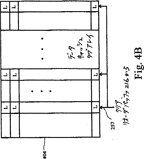
図4Bは、図4Aに示したタグエントリを含むデータキャッシュタグアレイを示し、これは、タグエントリのロックビットに対するクリアリングメカニズムを含む。
本発明に関してはさまざまな修正例および変形例が考えられるが、本発明の特定の実施例を例示の目的で図面に示しかつ以下に詳細に説明する。但し、それら図面および詳細な説明は本発明をその開示した特定の形に限定することを意図するものではなく、反対に、本発明は添付の請求の範囲で規定される本発明の精神および範囲内に含まれるすべての修正例、等価物および変形例を網羅するものである。
発明の詳細な説明
ここで図1を参照して、本発明に従ったロード/ストアユニット222およびデータキャッシュ224を含むスーパースカラマイクロプロセッサ200のブロック図が示される。図1の実施例において示されるように、スーパースカラマイクロプロセッサ200は、命令キャッシュ204に結合されたプリフェッチ/プリデコードユニット202および分岐予測ユニット220を含む。命令整列ユニット206は、命令キャッシュ204と複数のデコードユニット280A〜208F(集合的にデコードユニット208と称される)に結合される。各デコードユニット208A〜208Fは、それぞれのリザベーションステーションユニット210A〜210F(集合的にリザベーションステーション210と称される)に結合され、各リザベーションステーション210A〜210Fは、それぞれの機能ユニット212A〜212F(集合的に機能ユニット212と称される)に結合される。デコードユニット208、リザベーションステーション210、および機能ユニット212はさらに、リオーダバッファ216、レジスタファイル218およびロード/ストアユニット222に結合される。最後に、データキャッシュ224はロード/ストアユニット222に結合するよう示され、MROMユニット209は命令整列ユニット206に結合するよう示される。
一般に、命令キャッシュ204は、命令がデコードユニット208にディスパッチされるのに先立ってそれら命令を一時的にストアするよう提供された高速のキャッシュメモリである。一実施例においては、命令キャッシュ204は、各々が16バイト(ただし、各バイトは8ビットを含む)のラインで編成された、最高32キロバイトの命令コードをキャッシュするよう構成されている。動作中、命令コードはプリフェッチ/プリデコードユニット202を介してメインメモリ(図示せず)からコードをプリフェッチすることによって、命令キャッシュ204に提供される。なお、命令キャッシュ204はセットアソシアティブ構成、フルアソシアティブ構成、またはダイレクトマップ構成として実装することが可能である。
プリフェッチ/プリデコードユニット202は、メインメモリから命令コードをプリフェッチして、命令キャッシュ204内にストアするよう提供される。一実施例においては、プリフェッチ/プリデコードユニット202はメインメモリから命令キャッシュ204内へと、64ビット幅のコードをバーストするよう構成される。なお、プリフェッチ/プリデコードユニット202では、さまざまな種類のコードプリフェッチ技術およびアルゴリズムが使用され得る。
プリフェッチ/プリデコードユニット202は、メインメモリから命令をプリフェッチする際に、命令コードの各バイトに関連する以下の3つのプリデコードビットを生成する。すなわち:開始ビット、終了ビット、および「機能」ビットである。プリデコードビットは、各命令の境界を示すタグを形成する。プリデコードタグもまた、所与の命令がデコードユニット208によって直接デコードすることが可能であるか、または、命令がMROMユニット209によって制御されるマイクロコード手順を呼出すことによって実行されねばならないか等の、付加的な情報を伝送することが可能である。これについては、以下により詳細に説明する。
表1は、プリデコードタグのエンコードの1例を示す。表に示すように、所与のバイトが命令の第1のバイトであった場合、そのバイトに対して開始ビットがセットされる。バイトが命令の最後のバイトであった場合、そのバイトに対して終了ビットがセットされる。特定の命令がデコードユニット208によって直接デコードすることが不可能な場合、命令の第1のバイトに関連する機能ビットがセットされる。これに対し、もし命令がデコードユニット208によって直接デコードすることが可能である場合には、命令の第1のビットに関連する機能ビットはクリアされる。特定の命令の第2のビットに対する機能ビットは、オペレーションコード(opcode)が第1のバイトである場合にクリアされ、opcodeが第2のバイトである場合にはセットされる。但し、opcodeが第2のバイトである状況においては、第1のバイトはプレフィックスバイトである。命令バイト数3〜8に対する機能ビット値は、そのバイトがMODRMもしくはSIBバイトであるか、または、そのバイトが変位データもしくは即値データを含むかどうかを示す。
命令整列ユニット206は、命令キャッシュ204からの可変バイト長命令を、デコードユニット208A〜208Fによって形成される固定の発行位置へとチャンネル分けするよう提供される。命令整列ユニット206は、命令キャッシュ204によって提供された命令バイトの3つのグループから、独立してかつ並列に命令を選択し、それらのバイトを予備発行位置の3つのグループへと配列する。発行位置の各グループは、命令バイトのそれら3つのグループのうち1つのグループに関連する。予備発行位置はその後合併されて、最終的な発行位置が形成される。それらの各々は、デコードユニット208のうち1つのユニットに結合される。
ロード/ストアユニット222およびデータキャッシュ224の詳細な説明を続ける前に、図1に示す例示的なスーパースカラマイクロプロセッサ200内で用いられる他のサブシステムに関する概観について説明する。図1に示した実施例について、デコードユニット208の各々は、上に記載した予め定められた高速経路命令を復号化するためのデコード回路を含む。さらに、各デコードユニット208A〜208Fは変位データおよび即値データを、対応するリザベーションステーションユニット210A〜210Fに経路付ける。デコードユニット208からの出力信号は、機能ユニットのためのビットコード化実行命令および、オペランドアドレス情報、即値データおよび/または変位データを含む。
図1のスーパースカラマイクロプロセッサは追い越し実行を支持する。したがってこのスーパースカラマイクロプロセッサは、リオーダバッファ216を用いてレジスタの読出および書込動作に関するオリジナルプログラムシーケンスの監視を続けて、レジスタのリネームを行ない、投機的な命令の実行および分岐の誤予測回復を可能にすることによって、精密な例外処理を容易にする。当業者には理解されるように、リオーダバッファ216内の一時的な記憶場所は、レジスタの更新に関連する命令のデコード時にリザーブされ、それにより、投機的なレジスタ状態をストアする。リオーダバッファ216は先入れ先出し構成で実現されてもよく、ここで、投機的な結論はそれらが確証されかつレジスタファイルに書込まれる間に、バッファの「最後部」へと移動し、したがって、バッファの「頭部」には新しいエントリのために空きがつくられる。リオーダバッファ216は他の特定の構成もまた可能であり、これをさらに以下に説明する。分岐予測が正しくない場合、誤予測された経路に沿った投機的に実行された命令の結果は、それらがレジスタファイル218に書込まれるまでにバッファ内で無効とすることができる。
デコードユニット208A〜208Fの出力に提供された即値データおよびビットコード化実行命令は、それぞれのリザベーションステーションユニット210A〜210Fに直接経路付けされる。一実施例においては、各リザベーションステーションユニット210A〜210Fは対応する機能ユニットへの発行を待つ最高3つの未決の(pending)命令について、命令情報(すなわち、ビットコード化実行ビットならびにオペランド値、オペランドタグおよび/または即値データ)を保持することが可能である。但し、図1の実施例に関しては、各デコードユニット208A〜208Fは専用のリザベーションステーションユニット210A〜210Fに関連し、各リザベーションステーションユニット210A〜210Fは同様に、専用の機能ユニット212A〜212Fに関連する。したがって、6つの専用の「発行位置」が、デコードユニット208、リザベーションステーションユニット210および機能ユニットによって形成されることになる。整列されかつデコードユニット208Aを介して発行位置0にディスパッチされた命令は、リザベーションステーションユニット210Aに渡されて、その後、機能ユニット212Aに渡されて実行される。同様に、整列されかつデコードユニット208Bにディスパッチされた命令は、リザベーションステーションユニット210Bにかつその後機能ユニット212Bに渡される、等である。
特定の命令のデコード時、もし要求されるオペランドがレジスタのロケーションである場合、レジスタアドレス情報はリオーダバッファ216およびレジスタファイル218に同時に経路付けされる。当業者には、x86レジスタファイルが8個の32ビットリアルレジスタ(すなわち典型的に、EAX、EBX、ECX、EDX、EDP、ESI、EDIおよびESPと称される)を含むことが理解されるであろう。リオーダバッファ216は、これらのレジスタの内容を変更しかつしたがって追い越し実行を可能にする、結果のための一時的な記憶場所を含む。リオーダバッファ216の一時的な記憶場所は、各命令についてリザーブされ、これがデコード時に、リアルレジスタのうち1つの内容を修正するよう決定される。したがって、特定のプログラムの実行中さまざまな時点において、リオーダバッファ216は所与のレジスタの投機的に実行された内容を含む、1または複数の場所を有し得る。もし所与の命令のデコードに続いて、リオーダバッファ216が所与の命令内でオペランドとして使用されたレジスタに割当てられた先行する1または複数の位置を有すると判定された場合、リオーダバッファ216は対応するリザベーションステーションを、1)最も新しく割当てられた場所の値か、または2)その値が先行する命令を実際に実行する機能ユニットによって未だ生成されていない場合には最も新しく割当てられた場所に対するタグに送る。もしリオーダバッファが所与のレジスタに対してリザーブされた場所を有する場合には、そのオペランド値(またはタグ)が、レジスタファイル218からではなくリオーダバッファ216から提供される。リオーダバッファ216の要求されるレジスタに対してリザーブされている場所がない場合には、その値はレジスタファイル218から直接とられる。もしオペランドがメモリ場所に対応する場合、そのオペランド値はロード/ストアユニット222を介してリザベーションステーションユニットに提供される。
最適なリオーダバッファの実現に関する詳細は、マイク・ジョンソン(Mike Johnson)による「スーパースカラマイクロプロセッサの設計(“Superscalar Microprocessor Design”)」、Prentice-Hall,Englewood Cliffs,New Jersey,1991内に、および、ウイット(Witt)等によって1993年10月29日に出願された、「高性能スーパースカラマイクロプロセッサ(“High Performance Superscalar Microprocessor”)」と題され、同時継続中の共通に譲渡された米国特許出願連続番号第08/146,382号内に記載されている。これらの文献はその全体が、ここに引用により援用される。
リザベーションステーションユニット210A〜210Fは、対応する機能ユニット212A〜212Fによって投機的に実行されるべき命令情報を一時的にストアするよう提供される。上述のように、各リザベーションステーションユニット210A〜210Fは、最高3つの未決の命令に関して命令情報をストアすることが可能である。6個のリザベーションステーション210A〜210Fの各々は、対応する機能ユニットによって投機的に実行されるべきビットコード化実行命令およびオペランドの値をストアする場所を有する。もし特定のオペランドが利用できない場合、そのオペランドに対するタグがリオーダバッファ216から提供されて、その結果が生成されるまで(すなわち、先行する命令の実行の完了まで)対応するリザベーションステーション内にストアされる。但し、機能ユニット212A〜212Fのうち1つによって命令が実行されると、その命令の結果はその命令を待ついずれかのリザベーションステーションユニット210A〜210Fに直接渡され、同時にその結果はリオーダバッファ216を更新するよう渡される(この技術は一般に、「結果前送り(result forwarding)」と称される)。要求されるオペランドのいずれかの値が利用可能となった後に、命令が機能ユニットに発行されて実行される。すなわち、もしリザベーションステーションユニット210A〜210Fのうち1つ内の未決の命令に関連するオペランドに、リオーダバッファ216内の先行する結果値の場所のタグが付けられており、これがその要求されるオペランドを修正する命令に対応している場合には、その命令は、その先行する命令に対するオペランド結果が得られるまで、対応の機能ユニット212には発行されない。したがって、命令が実行される順序は、オリジナルのプログラム命令のシーケンスの順序と同じでない場合があり得る。リオーダバッファ216は、リードアフタライト依存が生じる状況においても、データの一貫性が確実に保たれるようにする。
一実施例においては、機能ユニット212の各々は、加算および減算の整数算術演算および、シフト、回転、論理演算、ならびに分岐演算を実行するよう構成される。但し、浮動小数点演算に対処するために浮動小数点ユニット(図示せず)もまた用いられてもよい。
機能ユニット212の各々はまた、条件付き分岐命令の実行に関する情報を分岐予測ユニット220に提供する。もし分岐予測が正しくない場合、分岐予測ユニット220は誤予測された分岐に続いて命令処理パイプラインに入った命令をフラッシュして、プリフェッチ/プリデコードユニット202が命令キャッシュ204またはメインメモリから必要な命令をフェッチするようにする。但し、このような状況においては、オリジナルのプログラムシーケンス内の命令であって誤予測された分岐命令の後に生じる結果は、投機的に実行されてロード/ストアユニット222およびリオーダバッファ216内に一時的にストアされた結果を含め、廃棄される。最適な分岐予測メカニズムの構成例は周知である。
機能ユニット212によって生成された結果は、レジスタ値が更新されていればリオーダバッファ216に送られ、メモリ場所の内容が変更されていればロード/ストアユニット222に送られる。もしその結果がレジスタ内にストアされるべきである場合には、リオーダバッファ216はその命令がデコードされた際にレジスタの値に対してリザーブされていた場所にその結果をストアする。結果は、上述のように、未決の命令が、要求されるオペランド値を得るために先行する命令実行の結果を待っている場合には、リザベーションステーションユニット210A〜210Fにも送られる。
一般的に、ロード/ストアユニット222は機能ユニット212A〜212Fとデータキャッシュ224との間にインターフェイスを提供する。一実施例においては、ロード/ストアユニット222は未決のロードまたはストオのためのデータおよびアドレス情報に対して16個の記憶場所を備えたロード/ストアバッファを有して構成される。デコードユニット208は、ロード/ストアユニット222へのアクセスを調停する。バッファが一杯である(full)場合、デコードユニットはロード/ストアユニット222に未決のロードまたはストア要求情報のための空きができるまで待たなければならない。機能ユニット212はロード/ストアユニット222に対してロード/ストア命令ならびに関連するアドレスおよびデータ情報を提供する。ロード/ストアユニット222は、データキャッシュ224にアクセスして、非投機的ロード/ストア命令がキャッシュをミスした際にデータキャッシュ224がメインメモリからラインをフェッチするようにすることによって、ロード/ストア命令を実行する。ロード/ストアユニット222はロード命令に必要なデータをリオーダバッファ216に、および、そのデータを待っているであろうリザベーションステーション210に戻す。ストアデータはロード/ストアユニット222によってデータキャッシュ224内にストアされる。ロード/ストアユニット222はまた、未決のストア命令に対するロード命令の依存性のチェックを行なって、確実にデータの一貫性が保たれるようにする。
データキャッシュ224は、ロード/ストアユニット222とメインメモリサブシステムとの間で転送されるデータを一時的にストアするよう提供される、高速のキャッシュメモリである。一実施例においては、データキャッシュ224は32本のバイトラインを有する8個のウェイのセットアソシアティブ構造内に最高で32キロバイトのデータをストアする容量を有する。但し、データキャッシュ224は、セットアソシアティブ構成を含む、さまざまな具体的なメモリ構成で実現することが可能である。
ここで図2に移って、本発明の一実施例を用いるロード/ストアユニット222のいくつかの重要な構成要素を描いた図が示される。ロード/ストアユニット222は、機能ユニット212に結合されてロード/ストア命令、アドレスおよびデータ情報を提供するための入力バス250を有する。入力バス250は、情報をロード/ストアバッファ251に伝達する。ロード/ストアバッファ251は、未処理のロード/ストア命令に関連する情報をストアする。リクエストバス253は、出力制御回路255の制御下、マルチプレクサ回路254によって選択されたとおり、データキャッシュ224にロード/ストア要求を伝達する。データキャッシュから戻るのがヒット/ウェイバス256であって、これはロード/ストアバッファ251に結合される。ヒット/ウェイバス56上で、ロード/ストアユニット222はデータキャッシュ224のヒット/ミス情報およびウェイ値を受取る。データキャッシュ224において、ヒットはリクエストバス253上で伝達されたリクエストについて検出される。リオーダバッファ216からのクリア信号ライン257は、ロード/ストアバッファ251に関連する回路を制御するよう結合される。
通常、ロード/ストアユニット222はロードまたはストアメモリリクエストを選択して、リクエストバス253上でデータキャッシュ224に伝送する。関連するバッファ記憶場所内の「チェックされたビット」は、現時点におけるリクエストがデータキャッシュ224をヒットする場合にセットされる。チェックされたビットは、その命令が有効であってクリア信号ライン257にクリア信号がアサートされない限り、セットされたままである。また、現時点におけるリクエストアドレスがヒットするウェイを示すデータキャッシュ224からのウェイ値は、ウェイフィールド内の関連するバッファ記憶場所内にストアされる。現時点のリクエストに関連するキャッシュ情報で現時点のリクエストのロード/ストアバッファ記憶場所を更新するのは、以下の3つの目的のためである。すなわち:1)データキャッシュをミスするロード命令を、そのミス情報で更新する、2)ストア命令を、書込がその間に発生する第2のサイクルアクセスのためのヒットおよびウェイで更新する、および3)「ロード-op-ストア」命令の一部分であるストア命令を、関連するロード命令のウェイおよびヒット値で更新する。これにより、そのストアがデータキャッシュ224への1回のみのアクセスで実行できるようになる。
ロード-op-ストア命令は、メモリ場所をソースおよびターゲットの双方として使用する、x86命令である。換言すれば、ロード-op-ストア命令のオペランドのうち1つはメモリ場所であって、ロード-op-ストア命令の結果は、そのメモリ場所内に記憶される。ロード-op-ストア命令は、スーパースカラマイクロプロセッサ200上で実行される際には、ロードおよびストア命令の双方としてロード/ストアユニット222にディスパッチされる。ここで、同じリオーダバッファタグがそれら双方に関連する。ロードおよびストア命令は、ロード/ストアバッファ251内の同じ記憶場所に記憶される。キャッシュのヒットおよびウェイ情報が、ロード-op-ストア命令のロード部分が実行される際にそのストア部分のために記録され、通常の2クロックサイクルストアアクセスの第1のクロックサイクルを排除することが可能となる。ロード-op-ストア命令のロード部分の実行とストア部分の実行との間のクロックサイクルにおいて、関連するデータキャッシュラインがそのデータキャッシュ内にストアされたままであることが重要である。この機能は、以下により詳細に説明するロックビットの使用によって実現される。
図2の実施例に示されるように、ロード/ストアバッファ251は、ロード/ストア命令に関連する。リオーダバッファタグ(図2においてはTAGフィールドと示される)と、チェックされたビット(Cフィールド)と、ウェイフィールド(Wフィールド)とを含む、記憶場所の線形アレイである。一実施例においては、ロード/ストアバッファ251は16個の記憶場所で構成される。他の情報は各ロード/ストアバッファエントリ内に記憶されるが、これは以下により詳細に説明する。論理回路のブロックは各記憶場所に関連し、チェックされたビットを各クロックサイクルで更新する。
1エントリに関連する論理回路の実施例を、ANDゲート258、259および261、ならびにORゲート260として図2に示す。ロード/ストアバッファ251内の各記憶場所について、同様の回路が作成される。ANDゲート261はリクエストバス253上のリクエストのバッファエントリをデコードする。もしこのバッファエントリが論理回路のこのグループに関連するバッファエントリと合致する場合、これは更新が可能である。ANDゲート261の出力は、エントリが更新可能である場合にハイとなる。ANDゲート258は、ANDゲート261の出力およびキャッシュからのヒットビットを受ける。ANDゲート258はORゲート260への入力のうち1つを形成し、これが記憶場所内のチェックされたビットをセットまたはクリアする。したがって、もしこのバッファエントリが現時点においてデータキャッシュ224にアクセスしておりかつそのアクセスがヒットする場合に、ANDゲート258(かつしたがってORゲート260)の出力は論理1であり、チェックされたビットがセットされる。ANDゲート259は、チェックされたビットの現時点における状態およびリオーダバッファ216からのクリア信号ライン257を受ける。クリア信号ライン257上で伝達されるクリア信号は、命令のフローを予測された経路から変更されるような例外、分岐誤予測または他の事象が起きる度に、リオーダバッファ216によってアサートされる。この種の事象が起こった場合、ロード/ストアバッファ内の命令のうちいくつかをロード/ストアユニット222とリオーダバッファ216(図示せず)との間のメカニズムを介してキャンセルすることが必要となる場合がある。したがって、チェックされたビットは、ロックビットがデータキャッシュ224内でクリアされるために、ロード/ストアバッファ251内でクリアされる(以下に詳細に説明する)。ANDゲート259はこのような機能を提供する。チェックされたビットは、クリア信号がアサートされない限りセットされたままであるが、アサートされた場合にはチェックされたビットはクリアされる。
マルチプレクサ254および出力制御ユニット255は、所与のクロックサイクルにおいてデータキャッシュ224へのアクセス要求を選択するのに使用される。一実施例においては、最高2つのリクエストが各クロックサイクルで選択される。本実施例においては、出力制御ユニット255はロード/ストアバッファ251から動作を選択するのに、優先度方式を実行する。ここで、もはや投機的ではないストア命令および、もはや投機的ではなくかつデータキャッシュをミスしたロード命令には高い優先順位が与えられ、投機的であるロード命令には低い優先順位が与えられる。但し、マルチプレクサ回路254が、リクエストバス253上に転送されるリクエストを生成する複数のマルチプレクサ回路として実装されてもよい。リクエストバス253は、リクエストがロードタイプであれストアタイプであれそのリクエストに関連する少なくともアドレスと、ウェイ値と、チェックされたビットと、ストアリクエストのためのストアデータとを伝達する。データキャッシュ224は、チェックされたビットがセットされていれば、関連するウェイ値によって選択されかつリクエストアドレスによってインデックスされたキャッシュライン内にデータを記憶するよう構成される。もしチェックされたビットがセットされていない場合、データキャッシュ224はキャッシュのインデックスされたラインを読出して、そのリクエストアドレスに関してキャッシュヒットをチェックする。一実施例においては、ロード-op-ストアビットはロードリクエストに対して伝達される(これについては以下に説明する)。
ロード/ストアバッファ251は、実施例によってそのエントリの数が変化し得る。さらに、ロード/ストアバッファ251は、別個のロードバッファおよびストアバッファとして構成されてもよく、この場合にはロードバッファはすべてのロード命令を記憶しかつストアバッファはすべてのストア命令を記憶する。さらに、リクエストバス253上では1クロックサイクル当たり2つ以上のリクエストが転送されてもよい。
別の実施例においては、データキャッシュ224にアクセスするアドレスは、ロード/ストアバッファ251内に記憶されたアドレスと比較される。この実施例は、2サイクルアクセスを排除することが可能なストア命令がロード-op-ストア命令のストア部分ではなくともよいという点において、先の実施例よりもより一般的である。しかし、キャッシュのロッキングはより複雑である。アクセスされたキャッシュラインに関連するロックビットは、チェックされたビットがキャッシュアクセスによってセットされている場合にはセットされる必要がある。これは、ロードがロード-op-ストア命令の一部分であるという事実に基づいたロッキングとは異なる。この実施例では通常、アクセスがその間に行なわれるクロックサイクルに続くクロックサイクル内で、キャッシュラインがロックされる。
ここで図3に移って、ロード/ストアバッファ251の一実施例について、ロード/ストアバッファ記憶場所内のビットフィールドの図が示される。フィールド300は、その記憶場所のためのリオーダバッファタグと、セットされている場合にその記憶場所が現時点において有効なロードまたはストア命令を記憶していることを示す有効ビットを含む。フィールド301は、機能ユニット212によって提供される、ロードまたはストア命令に関連するアドレスを記憶する。フィールド301にも有効ビットが含まれ、これはセットされている場合には、アドレスが有効であることを示す。出力制御ユニット255は、このアドレス有効ビットがセットされるまでデータキャッシュ224にアクセスするためのロード/ストア命令を選択することはない。フィールド302は、ストア命令に関連するデータおよび、セットされている場合にそのデータフィールドが有効であることを示す有効ビットを含む。ビット303は上述のチェックされたビットであって、フィールド304は上に記載したウェイフィールドである。ビット305は、セットされている場合にロード命令がロード-op-ストア命令のロード部分であることを示す、ロード命令のために使用されるビットである。このビットは、以下に説明するように、関連するキャッシュラインに対してロックビットをセットすべきかどうかを判定するのに使用される。但し、ロード/ストアユニット222の種々の実施例によって、他のビットが記憶場所に付加されてもよい。たとえば、命令がデータキャッシュミスであることを示すミスビット、および、命令がロード/ストアバッファ内の別の記憶場所に存在するストア命令に依存することを示す依存ビット等が付加されてもよい。
ここで図4Aに移って、一実施例におけるデータキャッシュタグユニット内のビットフィールドの図が示される。タグエントリは、関連するキャッシュラインの状態を示す状態フィールド401を有して構成される。一実施例においては、状態フィールド401は2ビット幅であって、キャッシュラインのためのMESI状態をエンコードする。当業者には理解されるように、MESI状態は、以下の状態をエンコードする。すなわち:修正されたまたは「汚損(dirty)」状態、この場合、キャッシュラインはメインメモリ内の関連するアドレスにストアされた内容に対して修正されており、したがって、そのキャッシュラインはデータキャッシュ224から取除かれる際にメインメモリへと書き戻されなければならない;排他状態、この場合、キャッシュラインはデータキャッシュ224内に記憶され、スーパースカラマイクロプロセッサ200を有するシステム内に構成された他のスーパースカラマイクロプロセッサ内にそのキャッシュラインの他のコピーが存在することはない;共有状態、この場合、キャッシュラインはデータキャッシュ224内に記憶されており、そのキャッシュラインの他のコピーが、スーパースカラマイクロプロセッサ200を有するシステム内に構成された他のスーパースカラマイクロプロセッサ内にストアされている可能性がある;および、無効状態、これは、関連するキャッシュラインが有効ではなくその中にストアされたバイトが使用されてはならないことを示す。
タグエントリのフィールド402は、エントリのタグを含む。上述のように、タグとは、メインメモリからのどのバイトがキャッシュライン内に記憶されているかを一意に識別するアドレスの部分である。一実施例においては、フィールド402は20ビット幅であって、キャッシュライン内に記憶されたバイトに関連するアドレスの20個の最上位ビットを含む。ビット403は上述のロックビットである。ビット403がセットされている場合、関連のキャッシュラインは、新しいキャッシュラインがメインメモリからフェッチされてもデータキャッシュ224から取除くことはできない。代わりにその行内の別のキャッシュラインが取除かれることになる。ロックビット403は、それに対応するロード-op-ストアビットセットを有するロード命令が関連のキャッシュラインにアクセスしてヒットすることがわかった際にセットされる。各タグエントリはロックビットを有して構成されているため、データキャッシュタグアレイ404は同時に複数のキャッシュラインについてロックを維持することが可能である。ロックビット403は、ストア命令が関連のキャッシュラインに実行される場合、または、クリア信号ライン257上で伝達されたクリア信号がリオーダバッファ216からアサートされた場合に、クリアされる(以下により詳細に説明する)。
特に注意を払うべきシナリオは、ロード-op-ストア命令のロード部分が、ロックビットがその中に既にセットされているキャッシュラインにアクセスする場合である。ロックビットがセットされているということは、先行するロード-op-ストア命令がそのロード部分でそのキャッシュラインにアクセスしたが、そのストア部分はまだ実行されていないことを示す。その先行するロード-op-ストア命令のストア部分がキャッシュラインにストアされると、上述のようにロックビットはクリアされる。したがって、ロックビットは、現時点におけるロード-op-ストア命令のストア部分がデータキャッシュ224にアクセスする前にクリアされ、関連するラインはキャッシュから取除くことが可能となる。ロード/ストアユニット222内の依存性チェックは、ロード部分がキャッシュにアクセスすることを防ぐ(図5〜70に関連して以下により詳細に説明する)。ロードデータは代わりに、ロード/ストアバッファ251によって提供される。一実施例においては、チェックされたビットは関連のストア部分に対してセットされることはない。したがって、ロード-op-ストア命令のストア部分は、このシナリオを完成するのに2つのデータキャッシュアクセスを必要とする。別の実施例においては、チェックされたビットが関連のストア部分に対してセットされ、かつ、1ビットがそのストア命令のためにセットされる。これは、ロード部分のためのデータ、すなわち、それがデータキャッシュ224にアクセスする際にロックビットをリセットしてはならないことを示すデータを提供する。この実施例においては、双方のストアがキャッシュへの単一のアクセス内で完了する。
ここで図4Bに移って、データキャッシュ224に関連するデータキャッシュタグアレイ404がブロック図で示される。一実施例においては、データキャッシュ224はセットアソシアティブ方式の8つのウェイであり、したがって、データキャッシュタグアレイ404の各行が図4Aに示した種類の8つのエントリを含む。キャッシュタグアレイ404はまた、クリア信号ライン257に結合され、それにより、クリア信号がアサートされるクロックサイクル中に、データキャッシュタグアレイ404内の各ロックビットがクリアされるようにする。クリア信号は、リオーダバッファ216がロード-op-ストア命令がキャンセルされたことを検出した際に、ロックビットがクリアされるようにする。キャンセルの理由は一例として、ロード-op-ストア命令に先立った分岐命令の分岐誤予測、および、ロード-op-ストア命令に先立った命令に関連する例外、等を含む。このようなキャンセルは、1クロックサイクル内で、ロード-op-ストア命令のロード部分の実行とその命令のストア部分との間に生じ得る。もし、ロックビットがロード-op-ストア命令によってセットされ、その命令が後にキャンセルされた場合、ロックビットがクリアされなければ、そのラインはデータキャッシュ224内にいつまでも残ったままとなる(これは、ロックビットをクリアするようストア命令がそのラインにストアされることがないためである)。したがって、ロード-op-ストア命令のロード部分の実行の後にその命令がキャンセルされた場合には、すべてのロックビットがクリアされる。上述のクリアが行われるときにキャンセルされなかったロード-op-ストア命令のストア部分がロード/ストアバッファ251(図2に示す)内に未だ存在する場合には、それらのストアはチェックされたビットがクリアされており(ANDゲート259と共に図2に示す)、その実行には2サイクルかかることになる。クリア信号がアサートされるようにする事象はスーパースカラマイクロプロセッサ内では比較的稀であり、したがって、殆どのロード-op-ストア命令は単一のサイクルストアの恩恵を被る。
なお、データキャッシュタグアレイ404は、データバイトを記憶するデータキャッシュアレイ224の一部として実装されてもよく、または、物理的に別個のアレイとして実装されてもよい。さらに、実施例によってデータキャッシュ224のアソシアティブ方式は異なる。データキャッシュ224がダイレクトマップ方式である実施例の場合、ロード/ストアバッファ251の記憶場所内のウェイフィールドは使用されない場合がある。
以上の開示に従って、スーパースカラマイクロプロセッサのためのロード/ストアユニットおよびデータキャッシュを説明した。ロード/ストアユニットとデータキャッシュとの組合せは、ロード-op-ストア命令のストア部分がデータキャッシュへの単一クロックサイクルのアクセスで実行することができるようにする。これは、ストアによって典型的に関連のキャッシュラインをサーチするためにおよびデータをストアするためにそれぞれ使用される、2つのクロックサイクルとは対照的である。したがって、殆どのロード-op-ストア命令から1データキャッシュアクセスサイクルを取除くことによって、より高い性能が達成されるようになる。
以上の開示が完全に理解されれば、当業者には種々の変形および修正例が明らかとなろう。以下の請求の範囲は、そのようなすべての修正例および変形例を包含するものと解釈されたい。 Background of the Invention
1.Field of Invention
The present invention relates to the field of superscalar microprocessors, and more particularly to load / store units and data caches in superscalar microprocessors.
2.Explanation of related technology
Superscalar microprocessors achieve high performance by executing multiple instructions simultaneously within one clock cycle and by identifying the shortest possible clock cycle that fits the design. As used herein, the term “clock cycle” refers to a time interval during which a pipeline stage of a microprocessor performs a predetermined function. At the end of the clock cycle, the resulting value is sent to the next pipeline stage.
Because a superscalar microprocessor executes multiple instructions per clock cycle and the clock cycle is short, providing a superscalar microprocessor with instructions and data requires a high bandwidth memory system (ie, in a short period of time). What is needed is a memory system that can provide a large number of bytes. If a high-bandwidth memory system is not used, the microprocessor will waste many clock cycles waiting for instructions or data to be provided, depending on the received instructions and / or received data. The instruction will be executed in a relatively small number of clock cycles. Overall performance is therefore degraded by multiple idle clock cycles. However, a superscalar microprocessor is typically configured in a computer system with a large main memory comprised of dynamic random access memory (DRAM) cells. DRAM cells are characterized by access times that are much longer than the clock cycles of modern superscalar microprocessors. DRAM cells also typically transmit stored bytes to a superscalar microprocessor via a relatively thin output bus. Accordingly, DRAM cells provide a memory system that provides a relatively small number of bytes in a relatively long time period and cannot form a high bandwidth memory system.
Superscalar microprocessors are often configured with a cache because superscalar microprocessors are usually not configured in a computer system with a memory system that has sufficient bandwidth to provide instructions and data sequentially. The A cache is a plurality of blocks of storage locations that are configured on or coupled to the same silicon substrate as the microprocessor. Those blocks of memory locations are used to hold previously fetched instruction or data bytes. These bytes can be quickly transferred from the cache to the destination (register or instruction processing pipeline). This usually requires 1 or 2 clock cycles, as opposed to multiple clock cycles being required to transfer bytes from the DRAM main memory.
The cache may be organized into an “associative” structure. In an associative structure, a block of storage locations is accessed as a two-dimensional array having rows and columns. When searching a cache to find a byte that exists at an address, a number of bits from that address are used as an “index” into the cache. This index selects a particular row in the two-dimensional array. Thus, the number of address bits required for the index is determined by the number of rows configured in the cache. The address associated with the byte stored in multiple blocks of a row is examined to determine if any address stored in that row matches the requested address. If a match is found, the access is called a “hit” and the cache provides the relevant bytes. If no match is found, the access is called a “miss”. When a miss is detected, those bytes are transferred from the memory system into the cache. The address associated with the byte stored in the cache is also stored. These stored addresses are referred to as “tags” or “tag addresses”.
A block of memory organized in a row forms a column of that row. Each block of memory is called a “way” and a plurality of ways constitute a row. A way is selected by providing a way value to the cache. The way value is determined by examining tags for a row and finding a match between one of those tags and the requested address. A cache designed with one way per line is referred to as a “direct map cache”. In a direct-mapped cache, the tag must be examined to determine if the access is a hit, but this tag check is used to select which bytes are forwarded to the cache output. Not needed.
Both direct-mapped and associative caches are used in high frequency (ie, short clock cycle) superscalar microprocessors. For either type of cache, if the cache is configured with a single port, one read or one write can be performed within one clock cycle. Even when the cache is composed of a plurality of ports, it is usually impossible to read and write the same block of the memory within the same clock cycle. Caches are large, usually requiring the majority (if not all) of one clock cycle to perform one read or one write due to the large capacity of the cache array and other well-known characteristics It has the following structure. In addition, reading and writing to the same location in the memory within one clock cycle requires the array to be very large and slow, thus having a significant negative impact on the clock cycle time and the silicon area of the superscalar microprocessor. Effect.
Because of the requirement that a cache memory location cannot be read and written within the same clock cycle, two cache accesses are required to accomplish the store instruction. In the first cache access, the cache is read to see if the address associated with the store instruction hits. If the address hits, the store data is written into the cache using the second cycle. If the address misses, the byte associated with that address is transferred into the cache. After the bytes are transferred, the store instruction accesses the cache again and writes the store data into the cache. A solution to the problem of store instructions that require at least two cache access cycles is desired.
Summary of the Invention
The problems as described above are largely solved by a data memory unit using a load / store unit and a data cache according to the present invention. The load / store unit consists of a load / store buffer with one way field and checked bits for each buffer storage location. For load-op-store instructions, when the load portion of the instruction accesses and hits the data cache, the checked bit of the storage location that stores the store portion of the instruction is set. Further, the way field of the storage location is set to the way of the data cache in which the load portion hits. The data cache is configured to have a locking mechanism for each cache line stored in the data cache. When the load portion of a load-op-store instruction is executed, the associated line is locked so that the line remains in its data cache until the store instruction is executed. In this way, the store portion of the load-op-store instruction will reliably hit the data cache in the way indicated by the way field associated with that store portion.
This load / store unit and data cache advantageously reduce the store portion of the load-op-store instruction from two clock cycles of data cache access to one clock cycle of data cache access. The performance of superscalar microprocessors using such data memory units can be improved by allowing more data cache access in a given set of clock cycles in which load-op-store instructions are executed. Is possible.
In general, the present invention relates to a data memory unit including a load / store unit and a data cache. The load / store unit is configured to execute load and store instructions and includes a first plurality of storage locations configured to store outstanding store instructions and associated store data. Each of the plurality of storage locations is configured to store a checked bit. The data cache includes a second plurality of storage locations coupled to the load / store unit and configured to store the cache line. The data cache locks the cache line stored in the second plurality of storage locations so that the cache line remains stored in the plurality of storage locations at least until the clock cycle when the lock is released. It is comprised so that.
The invention further relates to a method for storing store data in the data cache without having to first check whether the data cache hits an address associated with the store data. The method includes storing the store data in a data cache during a first clock cycle during which a checked bit associated with the store data is set.
[Brief description of the drawings]
Other objects and advantages of the present invention will become apparent upon reading the following detailed description with reference to the accompanying drawings. In the figure:
FIG. 1 is a block diagram of a superscalar microprocessor including a load / store unit and a data cache according to the present invention.
FIG. 2 is a diagram illustrating some of the internal components of a load / store unit including a load / store buffer according to the present invention.
FIG. 3 shows the bit field of the storage location of the load / store buffer shown in FIG.
FIG. 4A shows a tag entry for a data cache according to the present invention.
FIG. 4B shows a data cache tag array that includes the tag entry shown in FIG. 4A, which includes a clearing mechanism for the lock bit of the tag entry.
While various modifications and variations are possible in connection with the present invention, specific embodiments of the present invention are shown in the drawings for purposes of illustration and are described in detail below. However, the drawings and detailed description are not intended to limit the invention to the particular form disclosed, but on the contrary, the invention is defined by the spirit and scope of the invention as defined by the appended claims. All modifications, equivalents, and variations included therein are intended to be covered.
Detailed Description of the Invention
Referring now to FIG. 1, a block diagram of a
In general, instruction cache 204 is a high speed cache memory that is provided to temporarily store instructions prior to being dispatched to decode unit 208. In one embodiment, instruction cache 204 is configured to cache up to 32 kilobytes of instruction code, each organized in a line of 16 bytes (where each byte includes 8 bits). In operation, instruction code is provided to instruction cache 204 by prefetching code from main memory (not shown) via prefetch / predecode unit 202. The instruction cache 204 can be implemented as a set associative configuration, a full associative configuration, or a direct map configuration.
A prefetch / predecode unit 202 is provided to prefetch instruction codes from main memory and store them in the instruction cache 204. In one embodiment, prefetch / predecode unit 202 is configured to burst a 64-bit wide code from main memory into instruction cache 204. Note that various types of code prefetch techniques and algorithms may be used in the prefetch / predecode unit 202.
The prefetch / predecode unit 202 generates the following three predecode bits associated with each byte of the instruction code when prefetching an instruction from the main memory. Namely: start bit, end bit, and "function" bit. The predecode bits form a tag indicating the boundary of each instruction. The predecode tag can also be such that a given instruction can be decoded directly by the decode unit 208, or the instruction must be executed by calling a microcode procedure controlled by the
Table 1 shows an example of encoding of the predecode tag. As shown in the table, if a given byte is the first byte of an instruction, the start bit is set for that byte. If the byte is the last byte of the instruction, the end bit is set for that byte. If a particular instruction cannot be directly decoded by the decode unit 208, the function bit associated with the first byte of the instruction is set. In contrast, if the instruction can be directly decoded by the decode unit 208, the function bit associated with the first bit of the instruction is cleared. The function bit for the second bit of a particular instruction is cleared when the operation code (opcode) is the first byte, and is set when the opcode is the second byte. However, in the situation where opcode is the second byte, the first byte is a prefix byte. The function bit value for the number of instruction bytes 3 to 8 indicates whether the byte is a MODRM or SIB byte, or whether the byte includes displacement data or immediate data.
Before continuing with a detailed description of the load /
The superscalar microprocessor of FIG. 1 supports overtaking execution. Therefore, the superscalar microprocessor continues to monitor the original program sequence for register read and write operations using the
Immediate data and bit-coded execution instructions provided at the outputs of the
When decoding a particular instruction, if the required operand is a register location, the register address information is routed to the
Details on implementing an optimal reorder buffer can be found in Mike Johnson's “Superscalar Microprocessor Design”, Prentice-Hall, Englewood Cliffs, New Jersey, 1991, and A series of commonly assigned US patent applications, entitled “High Performance Superscalar Microprocessor”, filed October 29, 1993 by Witt et al. No. 08 / 146,382. These documents are incorporated herein by reference in their entirety.
In one embodiment, each of the
Each of the
The result generated by the
In general, load /
The
Turning now to FIG. 2, a diagram depicting some important components of a load /
Typically, the load /
A load-op-store instruction is an x86 instruction that uses a memory location as both a source and a target. In other words, one of the operands of the load-op-store instruction is a memory location, and the result of the load-op-store instruction is stored in that memory location. As load-op-store instructions are executed on the
As shown in the embodiment of FIG. 2, load /
An example of a logic circuit associated with one entry is shown in FIG. 2 as AND
The number of entries in the load /
In another embodiment, the address accessing
Turning now to FIG. 3, a diagram of bit fields within a load / store buffer storage location for one embodiment of load /
Turning now to FIG. 4A, a diagram of a bit field within a data cache tag unit in one embodiment is shown. The tag entry includes a
The
A scenario to which particular attention should be paid is when the load portion of the load-op-store instruction accesses a cache line with the lock bit already set therein. A lock bit being set indicates that a previous load-op-store instruction accessed the cache line in the load portion, but the store portion has not yet been executed. When the store portion of the preceding load-op-store instruction is stored in the cache line, the lock bit is cleared as described above. Thus, the lock bit is cleared before the store portion of the current load-op-store instruction accesses the
Turning now to FIG. 4B, a data
It should be noted that the data
In accordance with the foregoing disclosure, a load / store unit and data cache for a superscalar microprocessor has been described. The combination of the load / store unit and the data cache allows the store portion of the load-op-store instruction to execute with a single clock cycle access to the data cache. This is in contrast to the two clock cycles that are typically used by the store to search for associated cache lines and to store data, respectively. Therefore, higher performance is achieved by removing one data cache access cycle from most load-op-store instructions.
Numerous variations and modifications will become apparent to those skilled in the art once the above disclosure is fully appreciated. The following claims should be construed to encompass all such modifications and variations.
Claims (16)
前記ロード/ストアユニットに結合されたデータキャッシュ(224)を含み、前記データキャッシュはキャッシュラインをストアするよう構成された第2の複数の記憶場所を含み、前記データキャッシュは前記第2の複数の記憶場所内にストアされたキャッシュラインをロックするよう構成されて、それにより、少なくとも前記ロックがリリースされるクロックサイクルまで前記複数の記憶場所内に前記キャッシュラインがストアされたままとなるようにし、かつ前記第1の複数の記憶場所のうち1つ内にストアされた前記チェックされたビットは、ロード命令が前記第1の記憶場所のうち前記1つ内にストアされたストア命令に関連するアドレスと同じキャッシュラインにあるロードアドレスで前記データキャッシュにアクセスするときにセットされ、前記チェックされたビットは、前記ロードアドレスが前記データキャッシュにヒットすることがわかるとセットされ、
前記データキャッシュは前記データキャッシュにおけるロードアドレスによってヒットされるように前記キャッシュラインをロックするように構成され、前記ロード/ストアユニットは、前記第1の複数の記憶場所のうち1つ内にストアされたストアデータを前記データキャッシュに書き込むとき、前記チェックされたビットがセットされれば、キャッシュのヒットをチェックすることなくストアデータを書き込むように構成され、前記データキャッシュは、前記データキャッシュに書き込まれているストアデータに応答して前記ロックを前記キャッシュライン上でリリースするように構成される、データメモリユニット。A load / store unit (222) configured to execute load and store instructions, wherein the load / store unit is configured to store a raw store instruction and associated store data. A location (251), and each of the plurality of storage locations is further configured to store a checked bit;
A data cache (224) coupled to the load / store unit, the data cache including a second plurality of storage locations configured to store a cache line, the data cache comprising the second plurality of storage locations; Configured to lock a cache line stored in a storage location so that the cache line remains stored in the plurality of storage locations at least until a clock cycle in which the lock is released; And the checked bit stored in one of the first plurality of storage locations is an address associated with a store instruction in which a load instruction is stored in the one of the first storage locations. When accessing the data cache with a load address in the same cache line as Is set, the check bit is, the load address is set and it can be seen that the hit to the data cache,
The data cache is configured to lock the cache line to be hit by a load address in the data cache, and the load / store unit is stored in one of the first plurality of storage locations. When the stored data is written to the data cache, if the checked bit is set, the store data is configured to be written without checking a cache hit, and the data cache is written to the data cache. A data memory unit configured to release the lock on the cache line in response to stored data .
Applications Claiming Priority (1)
| Application Number | Priority Date | Filing Date | Title |
|---|---|---|---|
| PCT/US1996/011988 WO1998002818A1 (en) | 1996-07-16 | 1996-07-16 | A data memory unit configured to store data in one clock cycle and method for operating same |
Publications (2)
| Publication Number | Publication Date |
|---|---|
| JP2001505327A JP2001505327A (en) | 2001-04-17 |
| JP3824657B2 true JP3824657B2 (en) | 2006-09-20 |
Family
ID=22255488
Family Applications (1)
| Application Number | Title | Priority Date | Filing Date |
|---|---|---|---|
| JP50596398A Expired - Fee Related JP3824657B2 (en) | 1996-07-16 | 1996-07-16 | Data memory unit configured to store data within one clock cycle and method of operation thereof |
Country Status (4)
| Country | Link |
|---|---|
| EP (1) | EP1005675B1 (en) |
| JP (1) | JP3824657B2 (en) |
| DE (1) | DE69636822T2 (en) |
| WO (1) | WO1998002818A1 (en) |
Families Citing this family (2)
| Publication number | Priority date | Publication date | Assignee | Title |
|---|---|---|---|---|
| US8495272B2 (en) * | 2006-11-29 | 2013-07-23 | International Business Machines Corporation | Method to save bus switching power and reduce noise in an engineered bus |
| US8127114B2 (en) * | 2007-03-28 | 2012-02-28 | Qualcomm Incorporated | System and method for executing instructions prior to an execution stage in a processor |
Family Cites Families (5)
| Publication number | Priority date | Publication date | Assignee | Title |
|---|---|---|---|---|
| US4513367A (en) * | 1981-03-23 | 1985-04-23 | International Business Machines Corporation | Cache locking controls in a multiprocessor |
| US5185871A (en) * | 1989-12-26 | 1993-02-09 | International Business Machines Corporation | Coordination of out-of-sequence fetching between multiple processors using re-execution of instructions |
| EP0459233A3 (en) * | 1990-05-29 | 1992-04-08 | National Semiconductor Corporation | Selectively locking memory locations within a microprocessor's on-chip cache |
| US5353425A (en) * | 1992-04-29 | 1994-10-04 | Sun Microsystems, Inc. | Methods and apparatus for implementing a pseudo-LRU cache memory replacement scheme with a locking feature |
| JPH07334428A (en) * | 1994-06-14 | 1995-12-22 | Toshiba Corp | Cache memory |
-
1996
- 1996-07-16 DE DE69636822T patent/DE69636822T2/en not_active Expired - Lifetime
- 1996-07-16 JP JP50596398A patent/JP3824657B2/en not_active Expired - Fee Related
- 1996-07-16 WO PCT/US1996/011988 patent/WO1998002818A1/en not_active Ceased
- 1996-07-16 EP EP96928006A patent/EP1005675B1/en not_active Expired - Lifetime
Also Published As
| Publication number | Publication date |
|---|---|
| DE69636822D1 (en) | 2007-02-15 |
| DE69636822T2 (en) | 2007-10-04 |
| EP1005675B1 (en) | 2007-01-03 |
| WO1998002818A1 (en) | 1998-01-22 |
| EP1005675A1 (en) | 2000-06-07 |
| JP2001505327A (en) | 2001-04-17 |
Similar Documents
| Publication | Publication Date | Title |
|---|---|---|
| US5761712A (en) | Data memory unit and method for storing data into a lockable cache in one clock cycle by previewing the tag array | |
| KR100708010B1 (en) | Storage buffers that forward data based on indexes and optional path matching | |
| US5249286A (en) | Selectively locking memory locations within a microprocessor's on-chip cache | |
| US5802588A (en) | Load/store unit implementing non-blocking loads for a superscalar microprocessor and method of selecting loads in a non-blocking fashion from a load/store buffer | |
| US6519682B2 (en) | Pipelined non-blocking level two cache system with inherent transaction collision-avoidance | |
| US5845323A (en) | Way prediction structure for predicting the way of a cache in which an access hits, thereby speeding cache access time | |
| KR100880686B1 (en) | Branch prediction with two levels of branch prediction cache | |
| US6240484B1 (en) | Linearly addressable microprocessor cache | |
| US5748932A (en) | Cache memory system for dynamically altering single cache memory line as either branch target entry or prefetch instruction queue based upon instruction sequence | |
| US6230260B1 (en) | Circuit arrangement and method of speculative instruction execution utilizing instruction history caching | |
| US7213126B1 (en) | Method and processor including logic for storing traces within a trace cache | |
| US6321326B1 (en) | Prefetch instruction specifying destination functional unit and read/write access mode | |
| US6092182A (en) | Using ECC/parity bits to store predecode information | |
| US9131899B2 (en) | Efficient handling of misaligned loads and stores | |
| JP2004503870A (en) | Flush filter for translation index buffer | |
| US20030074530A1 (en) | Load/store unit with fast memory data access mechanism | |
| US20070050592A1 (en) | Method and apparatus for accessing misaligned data streams | |
| US6453387B1 (en) | Fully associative translation lookaside buffer (TLB) including a least recently used (LRU) stack and implementing an LRU replacement strategy | |
| US5893146A (en) | Cache structure having a reduced tag comparison to enable data transfer from said cache | |
| US6446189B1 (en) | Computer system including a novel address translation mechanism | |
| US5787474A (en) | Dependency checking structure for a pair of caches which are accessed from different pipeline stages of an instruction processing pipeline | |
| EP0459233A2 (en) | Selectively locking memory locations within a microprocessor's on-chip cache | |
| US5951671A (en) | Sharing instruction predecode information in a multiprocessor system | |
| JP3732234B2 (en) | Method for selecting non-blocking load from load / store unit and load / store buffer realizing non-blocking load for superscalar microprocessor | |
| US5687350A (en) | Protocol and system for performing line-fill address during copy-back operation |
Legal Events
| Date | Code | Title | Description |
|---|---|---|---|
| A131 | Notification of reasons for refusal |
Free format text: JAPANESE INTERMEDIATE CODE: A131 Effective date: 20050920 |
|
| A601 | Written request for extension of time |
Free format text: JAPANESE INTERMEDIATE CODE: A601 Effective date: 20051219 |
|
| A602 | Written permission of extension of time |
Free format text: JAPANESE INTERMEDIATE CODE: A602 Effective date: 20060213 |
|
| A521 | Request for written amendment filed |
Free format text: JAPANESE INTERMEDIATE CODE: A523 Effective date: 20060317 |
|
| TRDD | Decision of grant or rejection written | ||
| A01 | Written decision to grant a patent or to grant a registration (utility model) |
Free format text: JAPANESE INTERMEDIATE CODE: A01 Effective date: 20060613 |
|
| A61 | First payment of annual fees (during grant procedure) |
Free format text: JAPANESE INTERMEDIATE CODE: A61 Effective date: 20060628 |
|
| R150 | Certificate of patent or registration of utility model |
Free format text: JAPANESE INTERMEDIATE CODE: R150 |
|
| FPAY | Renewal fee payment (event date is renewal date of database) |
Free format text: PAYMENT UNTIL: 20090707 Year of fee payment: 3 |
|
| FPAY | Renewal fee payment (event date is renewal date of database) |
Free format text: PAYMENT UNTIL: 20100707 Year of fee payment: 4 |
|
| FPAY | Renewal fee payment (event date is renewal date of database) |
Free format text: PAYMENT UNTIL: 20110707 Year of fee payment: 5 |
|
| LAPS | Cancellation because of no payment of annual fees | ||
| S111 | Request for change of ownership or part of ownership |
Free format text: JAPANESE INTERMEDIATE CODE: R313113 |
|
| S531 | Written request for registration of change of domicile |
Free format text: JAPANESE INTERMEDIATE CODE: R313531 |
|
| R350 | Written notification of registration of transfer |
Free format text: JAPANESE INTERMEDIATE CODE: R350 |