JP3816467B2 - Liquid crystal display - Google Patents
Liquid crystal display Download PDFInfo
- Publication number
- JP3816467B2 JP3816467B2 JP2003185408A JP2003185408A JP3816467B2 JP 3816467 B2 JP3816467 B2 JP 3816467B2 JP 2003185408 A JP2003185408 A JP 2003185408A JP 2003185408 A JP2003185408 A JP 2003185408A JP 3816467 B2 JP3816467 B2 JP 3816467B2
- Authority
- JP
- Japan
- Prior art keywords
- liquid crystal
- layer
- clc
- ccf
- substrate
- Prior art date
- Legal status (The legal status is an assumption and is not a legal conclusion. Google has not performed a legal analysis and makes no representation as to the accuracy of the status listed.)
- Expired - Fee Related
Links
- 239000004973 liquid crystal related substance Substances 0.000 title claims description 85
- 239000004986 Cholesteric liquid crystals (ChLC) Substances 0.000 claims description 151
- 239000011295 pitch Substances 0.000 claims description 72
- 239000000758 substrate Substances 0.000 claims description 62
- 238000000576 coating method Methods 0.000 claims description 3
- 239000011248 coating agent Substances 0.000 claims description 2
- 230000010287 polarization Effects 0.000 description 10
- 239000010409 thin film Substances 0.000 description 7
- 238000010521 absorption reaction Methods 0.000 description 5
- 239000011159 matrix material Substances 0.000 description 5
- 230000000694 effects Effects 0.000 description 4
- 230000003247 decreasing effect Effects 0.000 description 3
- 238000010030 laminating Methods 0.000 description 3
- 230000031700 light absorption Effects 0.000 description 3
- 239000002184 metal Substances 0.000 description 3
- 241000282412 Homo Species 0.000 description 2
- 230000005540 biological transmission Effects 0.000 description 2
- 239000003086 colorant Substances 0.000 description 2
- 230000005684 electric field Effects 0.000 description 2
- 239000010408 film Substances 0.000 description 2
- 238000000034 method Methods 0.000 description 2
- 238000002834 transmittance Methods 0.000 description 2
- 230000003098 cholesteric effect Effects 0.000 description 1
- 238000010586 diagram Methods 0.000 description 1
- AMGQUBHHOARCQH-UHFFFAOYSA-N indium;oxotin Chemical compound [In].[Sn]=O AMGQUBHHOARCQH-UHFFFAOYSA-N 0.000 description 1
- 239000011810 insulating material Substances 0.000 description 1
- 239000000463 material Substances 0.000 description 1
- 230000003287 optical effect Effects 0.000 description 1
- 229920000642 polymer Polymers 0.000 description 1
- 238000004064 recycling Methods 0.000 description 1
- 238000009751 slip forming Methods 0.000 description 1
- 238000007740 vapor deposition Methods 0.000 description 1
Images


Classifications
-
- G—PHYSICS
- G02—OPTICS
- G02F—OPTICAL DEVICES OR ARRANGEMENTS FOR THE CONTROL OF LIGHT BY MODIFICATION OF THE OPTICAL PROPERTIES OF THE MEDIA OF THE ELEMENTS INVOLVED THEREIN; NON-LINEAR OPTICS; FREQUENCY-CHANGING OF LIGHT; OPTICAL LOGIC ELEMENTS; OPTICAL ANALOGUE/DIGITAL CONVERTERS
- G02F1/00—Devices or arrangements for the control of the intensity, colour, phase, polarisation or direction of light arriving from an independent light source, e.g. switching, gating or modulating; Non-linear optics
- G02F1/01—Devices or arrangements for the control of the intensity, colour, phase, polarisation or direction of light arriving from an independent light source, e.g. switching, gating or modulating; Non-linear optics for the control of the intensity, phase, polarisation or colour
- G02F1/13—Devices or arrangements for the control of the intensity, colour, phase, polarisation or direction of light arriving from an independent light source, e.g. switching, gating or modulating; Non-linear optics for the control of the intensity, phase, polarisation or colour based on liquid crystals, e.g. single liquid crystal display cells
- G02F1/133—Constructional arrangements; Operation of liquid crystal cells; Circuit arrangements
- G02F1/1333—Constructional arrangements; Manufacturing methods
- G02F1/1335—Structural association of cells with optical devices, e.g. polarisers or reflectors
- G02F1/1336—Illuminating devices
- G02F1/13362—Illuminating devices providing polarized light, e.g. by converting a polarisation component into another one
-
- G—PHYSICS
- G02—OPTICS
- G02F—OPTICAL DEVICES OR ARRANGEMENTS FOR THE CONTROL OF LIGHT BY MODIFICATION OF THE OPTICAL PROPERTIES OF THE MEDIA OF THE ELEMENTS INVOLVED THEREIN; NON-LINEAR OPTICS; FREQUENCY-CHANGING OF LIGHT; OPTICAL LOGIC ELEMENTS; OPTICAL ANALOGUE/DIGITAL CONVERTERS
- G02F1/00—Devices or arrangements for the control of the intensity, colour, phase, polarisation or direction of light arriving from an independent light source, e.g. switching, gating or modulating; Non-linear optics
- G02F1/01—Devices or arrangements for the control of the intensity, colour, phase, polarisation or direction of light arriving from an independent light source, e.g. switching, gating or modulating; Non-linear optics for the control of the intensity, phase, polarisation or colour
- G02F1/13—Devices or arrangements for the control of the intensity, colour, phase, polarisation or direction of light arriving from an independent light source, e.g. switching, gating or modulating; Non-linear optics for the control of the intensity, phase, polarisation or colour based on liquid crystals, e.g. single liquid crystal display cells
- G02F1/133—Constructional arrangements; Operation of liquid crystal cells; Circuit arrangements
- G02F1/1333—Constructional arrangements; Manufacturing methods
- G02F1/1335—Structural association of cells with optical devices, e.g. polarisers or reflectors
- G02F1/133528—Polarisers
- G02F1/133543—Cholesteric polarisers
Landscapes
- Physics & Mathematics (AREA)
- Nonlinear Science (AREA)
- Mathematical Physics (AREA)
- Chemical & Material Sciences (AREA)
- Crystallography & Structural Chemistry (AREA)
- General Physics & Mathematics (AREA)
- Optics & Photonics (AREA)
- Polarising Elements (AREA)
- Optical Filters (AREA)
- Liquid Crystal (AREA)
Description
【0001】
【発明の属する技術分野】
本発明は、液晶表示装置(liquid crystal display device)に係り、さらに詳細に説明すればコレステリック液晶の特性を利用したCLC偏光板とCLCカラーフィルターを含む透過型カラー液晶表示装置に関する。
【0002】
【従来の技術】
一般的に、液晶表示装置の駆動原理は、液晶の光学的異方性と分極性質を利用する。前記液晶は構造が細くて長いために分子の配列に方向性を持っており、人為的に液晶に電界を印加して分子配列の方向を制御できる。したがって、前記液晶に印加される電界の大きさを任意に調節して液晶の分子配列が変わるようになれば、液晶層を通過して入射された光の偏光特性が変わるようになり、これから偏光板を通過した光の量が調節されて画像情報を表現できる。
【0003】
現在、液晶表示装置として、薄膜トランジスタと前記薄膜トランジスタに連結した画素電極がマトリックス方式で配列されたアクティブマトリックス液晶表示装置(AM−LCD)が解像度及び動画の具現能力が優秀で最も注目を浴びている。
【0004】
一般的な液晶表示装置を構成する基本的な部品である液晶パネルの構造を説明すれば次の通りである。図1は、一般的な液晶表示装置を概略的に示した図面である。図示したように、液晶表示装置11は、ブラックマトリックス6とサブカラーフィルター(赤、緑、青)8a、8b、8cを含んだカラーフィルター8と、カラーフィルター上に透明な共通電極18が形成された上部基板5と、画素領域Pと画素領域上に形成された画素電極17とスイッチング素子Tを含んだアレイ配線が形成された下部基板22で構成され、前記上部基板5と下部基板22間には液晶14が充填されている。
【0005】
前記下部基板22は、アレイ基板とも称し、スイッチング素子である薄膜トランジスタTをマトリックス形態に配置し、このような多数の薄膜トランジスタを交差してゲート配線13とデータ配線15が形成される。前記画素領域Pは、前記ゲート配線13とデータ配線15が交差して定義される領域である。前記画素領域P上に形成される画素電極17はインジウム−スズ−オキサイド(ITO)のように光の透過率が比較的優れた透明導電性金属を用いる。前述したようにして構成された液晶表示装置11の下部には前記液晶表示装置に光を提供する光源である背光装置(back light)(図示せず)が構成される。
【0006】
上述したアクティブマトリックス液晶表示装置の動作を説明すれば、スイッチング薄膜トランジスタTに信号が印加されると、データ信号が画素電極17に印加されて、信号が印加できない場合には画素電極17にデータ信号が印加できない。すなわち、前記液晶表示装置は、光をスイッチングする光変調器の一種である。
【0007】
一般的に、従来の液晶表示装置は、図面に示さなかったが、バックライトから放出される光を利用する構造で構成されており、前記バックライトから放出された光がカラーフィルターを透過して、画像に表現されるためには多数個の機能性薄膜を透過しなければならないために非常に非効率的な光変調器である。前記機能性薄膜には、バックライト光の偏光状態を調節する2枚の線形偏光板と、バックライト光を彩色するカラーフィルターなどがある。
【0008】
しかし、前記線形偏光板は、バックライト光の線形成分、すなわち一方向の線偏光光だけを透過させるためにバックライトから放出された光の約半分以下の成分だけを透過させることになり、バックライトを效率的に使用できない短所がある。すなわち、輝度が相当に落ちる問題がある。また、一般的に、液晶表示装置に使われるカラーフィルターは、吸収型カラーフィルターであって、前記カラーフィルターを透過する時もバックライトから放出される光の損失が多く発生するようになる。
【0009】
上記のように輝度が落ちる問題点を解決するためには、前記カラーフィルターの透過率を向上させなければならなく、これのためには前記カラーフィルターの色純度を低くめにしなければならないが、単純に色純度を低くめて輝度を向上させるには限界がある。
【0010】
上述した液晶表示装置における輝度の問題を解決するために、コレステリック液晶の特性を利用してコレステリック液晶(Cholestric LC;CLC)カラーフィルターを用いた液晶表示装置が研究/開発されている。前記コレステリック液晶カラーフィルターは、コレステリック液晶の選択反射特性を利用することを特徴とする。
【0011】
すなわち、コレステリック液晶の特性であるヘリカルピッチ(helicalpitch)によって光の透過及び反射される波長領域を調節できるので、画素領域別にヘリカルピッチを違うように調節してコレステリック液晶カラーフィルターを作ることができる。前述した特性を有したコレステリック液晶カラーフィルターは、一般吸収型カラーフィルターとは異なり選択反射特性を利用するので、吸収型カラーフィルターで消失される光を利用して光効率を高めることができる。
【0012】
図2は、従来のコレステリック液晶カラーフィルターを含んだ反射型液晶表示装置を概略的に示した断面図であって、その構成は次の通りである。図示したように、反射型液晶表示装置50は、透明な絶縁物質で構成された第1基板5及び第2基板22が相互に離隔して構成される。前記第2基板22の下部には光を吸収する光吸収層34を構成する。この時、前記光吸収層34は、光を吸収すればよく、光吸収用物質、例えばポリマーのような物質を前記第2基板22の背面に塗布して形成する方法がある。
【0013】
そして、前記第2基板22上にはコレステリック液晶を塗布した後パターニングして、赤緑青の各画素に対応して赤色と緑色と青色波長を各々反射させるコレステリック液晶(以下"CLC"と称す)カラーフィルター層24を形成する。前記CLCカラーフィルター(以下"CCF"と称する)層24の上部には透明な導電性金属を蒸着してパターニングし、第2電極17を形成する。前記第1基板5のうち前記第2基板22と対向する面には前述した透明な導電性金属を蒸着して第1電極18を形成し、前記第1基板5の上部には位相差板30と線偏光版32が順に構成される。前記第1基板5と第2基板22の間には液晶層14が介在される。
【0014】
先に説明したように、前記CCF層24は、コレステリック液晶をカラーフィルターとして用いたものであって、これは特定波長帯の右円偏光または左円偏光を選択的に反射/透過する特性を有する。すなわち、CLCカラーフィルターは、R、G、Bの各々に該当する波長領域を選択して、それぞれの中心波長に対して左、右ピッチ偏差が生じるように条件を調節してピッチ偏差に該当する波長領域から左円偏光または右円偏光された光を選択的に反射/透過させる特性を有するように形成される。
【0015】
つまり、可視光線のうち各画素に該当する前記カラーの固有な波長だけを選択的に反射させるように液晶のピッチを人為的に調節できる。この時、反射された光は、リサイクリングを通してR、G、Bの該波長領域に透過される。したがって、吸収型カラーフィルターが透過される波長帯以外に該当する光をすべて吸収するものとは異なり、前記CLCカラーフィルターは透過される光の量が多いので色純度と色再現性が良い長所がある。
【0016】
【発明が解決しようとする課題】
しかし、コレステリックカラーフィルター適用反射型液晶表示装置は、色純度または色再現性が良いが、CLCカラーフィルター層から反射される光以外には吸収層34によって吸収されるので光効率が良い方ではない。反面、前記CLCカラーフィルターを透過型として用いれば、反射される光以外の光を利用できるので輝度を改善する長所がある。
【0017】
したがって、本発明は、CLCカラーフィルターとCLC偏光板を含む透過型液晶表示装置を提案するものであって、前記偏光板のうちバックライトと近接した部分は長波長のピッチを有するようにし、それと反対の部分は短波長帯のピッチを有するようにして、高輝度(high brightness)と高コントラスト(high contrast)を具現するカラー液晶表示装置を提供することを目的とする。
【0018】
また、本発明は、前述したようなCLCカラーフィルターを含む液晶パネルにCLC偏光板と、前記CLCカラーフィルターと液晶層の間に線形偏光板と位相差板をさらに構成するが、前記CLC偏光板のうち前記バックライトと近接した一面は長波長のピッチを有するようにし他の面は短波長帯のピッチを有するようにして、高輝度と高コントラストを有するカラー液晶表示装置を提供することをその目的とする。
【0019】
【課題を解決するための手段】
前述した目的を達成するための本発明による液晶表示装置は、相互に向かい合って離隔された第1基板及び第2基板と;前記第1基板の外側の面に構成された第1偏光板と;前記第1基板と第2基板間に充填された液晶層と;前記第2基板の下部に構成されたバックライトと;前記第2基板とバックライトの間に構成されて、前記バックライトに近接して第1ピッチを有する第1部分と、前記第2基板の外側の面に近接して第2ピッチを有する第2部分と、前記第1部分及び第2部分間において前記第1ピッチから前記第2ピッチに順次変わる第3ピッチを有する第3部分で構成されるコレステリック液晶(CLC)偏光板を含み、前記第1ピッチは、長波長に対応するピッチを有するように構成すると共に、前記第2ピッチは、短波長に対応するピッチを有するように構成し、かつ前記第1ピッチは、前記第2ピッチより長いことを特徴とする。
【0020】
また、前記第2基板の内側面に構成されたCLCカラーフィルター(CCF)層をさらに含むことができる。
【0021】
前記CCF層とCLC偏光板の内部液晶のねじれた方向が相互に反対方向であり、前記CCF層が左円偏光された光を反射する場合、前記CLC偏光板は右円偏光された光を反射し、前記CCF層が右円偏光された光を反射する場合、前記CLC偏光板は左円偏光された光を反射する。
【0022】
前記第1基板及び第2基板は赤色、緑色、青色画素領域を有し、前記赤色、緑色、青色画素領域のCCF層は各々赤色、緑色、青色の光を透過させる。
【0023】
前記CCF層は第1CLC層及び第2CLC層を含んで、前記赤色画素領域にある前記第1CLC層及び第2CLC層は各々青色、緑色に対応するピッチを有し、前記緑色画素領域にある前記第1CLC層及び第2CLC層は各々青色、赤色に対応するピッチを有し、前記青色画素領域にある前記第1CLC層及び第2CLC層は各々緑色、赤色に対応するピッチを有する。
【0024】
一方、前記第1偏光板と液晶層間に位相差フィルムをさらに構成でき、この時、前記液晶層はOCB(optically compensated birefringence)モードである。
【0025】
また、前記第2基板の内側面に位相差板と前記位相差板の上部に第2偏光板をさらに含むことができ、前記第1偏光板及び第2偏光板は光を線偏光させる。そして、前記位相差板と前記第2基板間にCCF層をさらに含むことができ、この時、前記液晶層はTN(twisted nematic)モードである。
【0026】
前記位相差板と第2偏光板は前記CCF層上部にコーティングによって順に形成されることができ、前記CCF層とCLC偏光板の内部液晶のねじれた方向が相互に反対方向であるので、前記CCF層が左円偏光された光を反射する場合、前記CLC偏光板は右円偏光された光を反射し、前記CCF層が右円偏光された光を反射する場合、前記CLC偏光板は左円偏光された光を反射する。
【0027】
前記第1基板及び第2基板は赤色、緑色、青色画素領域を有し、前記赤色、緑色、青色画素領域のCCF層は各々赤色、緑色、青色の光を透過させて、前記CCF層は第1CLC層及び第2CLC層を含んで、前記赤色画素領域にある前記第1CLC層及び第2CLC層は各々青色、緑色に対応するピッチを有し、前記緑色画素領域にある前記第1CLC層及び第2CLC層は各々青色、赤色に対応するピッチを有し、前記青色画素領域にある前記第1CLC層及び第2CLC層は各々緑色、赤色に対応するピッチを有する。
【0028】
【発明の実施の形態】
以下、本発明による実施の形態を添付された図面を参照しながら詳細に説明する。
−−実施の形態−−
本発明は、CLCカラーフィルターと広帯域波長のCLC偏光板を構成すると同時に、前記コレステリック液晶のうち前記カラーフィルターと近接した部分は短波長帯域のピッチで構成し、バックライトに近接した部分は長波長帯域のピッチで構成することを特徴とする。
【0029】
図3は、本発明の第1の実施の形態による液晶表示装置を概略的に示した断面図である。図示したように、第1基板100と第2基板200を離隔して構成し、前記第1基板100と第2基板200の間には、特定波長帯の左円偏光を選択して反射するようにそのピッチが調節されたCLCカラーフィルター層202を形成する
(以下、コレステリック液晶を"CLC"と称してCLCカラーフィルターを"CCF"と称す)。
【0030】
この時、前記CCF層202は、各画素PR、PG、PBごとに相互に他の波長帯の左円偏光を反射するコレステリック液晶パターンを積層して構成する。続いて、前記CCF層202の上部には液晶層204を構成し、前記第1基板100の上部には位相差板102と第1偏光板104を続いて構成する。前記第2基板200の下部には第2偏光板であるCLC偏光板(polarizer)206と、このCLC偏光206板の下部にバックライト300を構成する。
【0031】
前述した構成において、前記CCF層202は、透過される光が赤、緑、青色を帯びるように構成されていて、CCF層202の選択反射波長帯はコレステリック液晶分子のピッチによって決定されるために、一ピクセルにおいてピッチの分布にしたがって反射される波長帯を調節できる。
【0032】
すなわち、再び説明すれば、人間が目で見られる可視光の波長領域は、400〜700nm間の小さい波長領域に限定される。前記のように人間が見られる光の波長帯を可視光線(可視領域)という。この時、前記可視光線のうち赤色は、660nm近辺の波長帯に該当し、緑色は530nmに該当し、青色は470nmの波長に該当する。すなわち、液晶のピッチを人為的に操作(増やしたり減らして)でき、このような人為的なCLCカラーフィルターは、可視光線のうち各ピクセルに該当する前記カラーの固有な波長だけを選択的に反射/透過させることによって高純度の色感を表示できるようにする。
【0033】
したがって、赤、緑、青三色の配置によりイメージが表現されるカラーフィルターを前述した波長の特性を利用して具現できる。このため、前記CCF層202は固有の色を吸収型カラーフィルターと比較して鮮明に表現できる長所がある。
【0034】
前記CCF層202の構成を説明すれば、赤色画素PRには緑色CCF(CCF(G))と青色CCF(CCF(B))を積層して構成し、緑色画素PGには赤色CCF(CCF(R))と青色CCF(CCF(B))を積層して構成し、青色画素PBには緑色CCF(CCF(G))と赤色CCF(CCF(R))を積層して構成する(この時、各CCFは特定の波長帯の左円偏光を反射するようにそのピッチが調節されたものである)。すなわち、前記CCF層202は、各画素別に他の波長帯の光を反射する第1CLC層及び第2CLC層202a、202bで構成される。このように構成すれば、赤色と緑色と青色画素PR、PG、PBから各々赤色と緑色と青色波長帯に該当する光を観察できる。
【0035】
前記CLC偏光板206は、バックライト300から生成された光を右円偏光または左円偏光される光に位相を変える実質的に偏光板の機能をする。したがって、一度照射された光のうち透過できなく反射された光が前記偏光板により再反射される間に偏光成分が変わって前記CLCカラーフィルターを通過できるようになる。これは線形偏光板とは異なり透過できなかった光を多次の反射過程を経て外部に出射できるようにするために高輝度を具現できる。
【0036】
本発明では、前記CLC偏光板206が広帯域(380nm〜780nm)の特性を有し、また、バックライト300から入射された光のうち右円偏光を反射する特性を有する。これは、前記CCF層202が特定波長帯において左円偏光を反射するようにしたものと比較して反対の特性を有するように構成したものである。
【0037】
また、前記CLC偏光板206は、前記バックライト300に近接した第1部分206a、前記CCF層202に近接した第2部分206bと前記第1部分及び第2部分間の第3部分206cを有する。この時、前記CLC偏光板206の第1部分206aには長波長に対応するピッチを有するように構成し、第2部分206bには短波長のピッチを有するように構成する。
【0038】
前述したような構成で製作された本発明による液晶表示装置における光の偏光特性を調べてみる(電圧がオン状態の場合、緑色を表現する一画素を例に挙げて説明する)。まず、バックライト300を出射した光は、前記CLC偏光板206ににより、右円偏光成分は再びバックライト300側に反射され、左円偏光が透過される。
【0039】
続いて、前記左円偏光された可視光領域帯の光は、まず、前記第2CLC層202bの赤色CCF(CCF(R))により、赤色に該当する左円偏光された光が再びCLC偏光板206に反射される。続いて、赤色CCF(CCF(R))を通過した光のうち前記第1CLC層202aの青色CCF(CCF(B))により青色波長帯の左円偏光が反射される。
【0040】
したがって、緑色波長帯の左円偏光だけが液晶層を通して外部に出射することによって緑色画素PGは緑色を表現する。このような原理は、赤色と青色を表現する画素PR、PBにも同一に適用される。前記CCFを透過した光は、上部の位相差板102と第1偏光板104を通して外部に出射される。
【0041】
前述したように構成された本発明による透過型液晶表示装置は高いコントラスト比を有することを特徴とする。これに対する実験結果を、表1を参照して説明する。
【0042】
【表1】
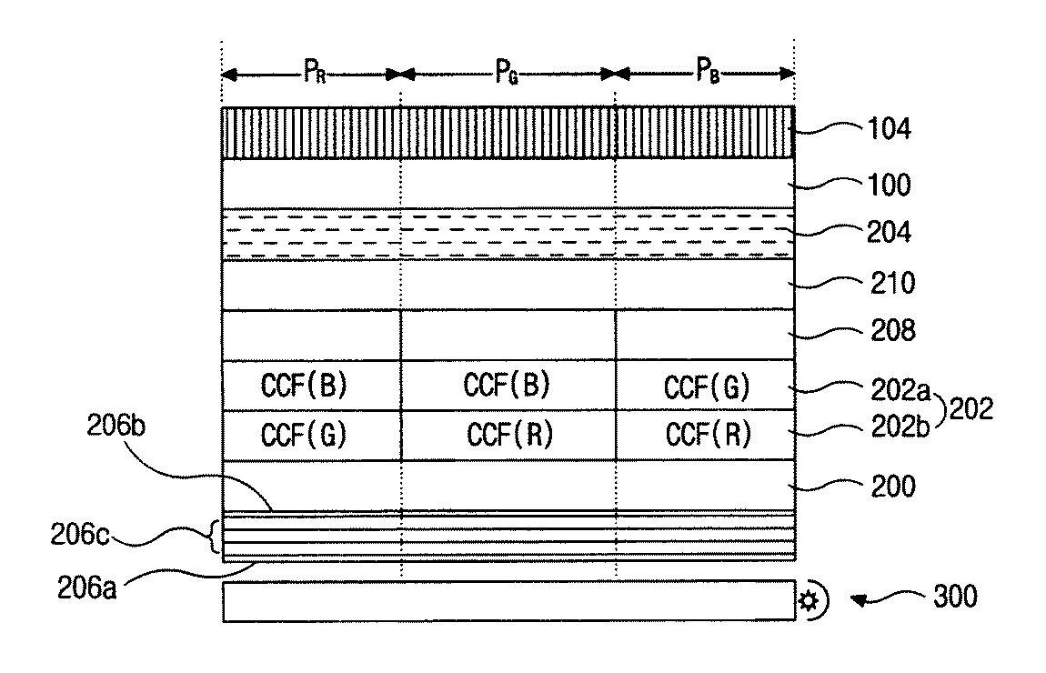
表1は、緑色を表現する画素に構成された青色CCFと赤色CCFの位置を別にして、それぞれの構成に対して前記CLC偏光板のうちバックライトに近接した部分を長波長帯のピッチに合うように構成した場合と、短波長帯のピッチに合うように構成した場合、対照比(contrast ratio:コントラスト比)を実験を通して比較したものである。
【0044】
ここで、前記実験に常用されたCLC偏光板の条件を簡単に説明する。前記CLC偏光板206は、No(ordinary index)を1.5にNe(extra−ordinary index)を1.68になるようにして、フィルムの厚さは30μmに製作した。前記CLC偏光板206うちバックライト300に近接した面を第1部分206aと称し、前記CCF層202に近接した面を第2部分206bと称す。
【0045】
このようなCLC偏光板206を含んだ液晶表示装置を下記の第1テスト、第2テストで実験した。まず、第1テストでは、第1CLC層202aは、青色CCF(CCF(B))に、第2CLC層202bは赤色CCF(CCF(R))に構成し、第2テストでは、第1CLC層202aは赤色CCF(CCF(R))に、第2CLC層202bは青色CCF(CCF(B))に構成して実験した。
【0046】
この時、前記CLC偏光板206両面のうちバックライト300に近接した第1部分206aが長波長に対応するピッチ(長ピッチ)を有する場合(第1タイプ)と短波長に対応するピッチ(短ピッチ)を有する場合(第2タイプ)を比較する。
【0047】
前記積層された各CCF層202の積層順序を変えて実験した理由は、前記CLC偏光板206の構成を拡大適用できるという例を見せるためである。表において、90/0と0/90等は、カラーフィルターである第1CLC層202aと第2CLC層202bに属する各液晶ディレクタ(director)の相対的位置を意味する。
【0048】
表から分かるように、前記バックライト300に近接したCLC偏光板の第1部分202aが長波長に対応するピッチを有する場合(第1タイプ)が前記例を挙げたすべての場合にバックライトに近接した第1部分202aが短波長に対応するピッチを有する場合(第2タイプ)より高い対照比を見せることが確認できる。
【0049】
このような理由は、明状態(White state)の絶対輝度はほとんど同じだが、暗状態(Black state)の輝度値がさらに小さくなる(ブラック状態をさらに暗くさせる)に従って対照比が増加されるためであることが分かった。
【0050】
前述した構成では、CCFを特定波長帯の左円偏光を反射するものであって、前記CLC偏光板は特定の波長帯の右円偏光を反射する構成として例を挙げたが、各々を反対の特性を有するように構成しても同一な特性を示す。
【0051】
一方、液晶表示装置の対照比は、本発明の第2実施の形態でさらに改善される。本発明の第2の実施の形態は、コレステリック液晶カラーフィルターと広帯域波長帯のコレステリック液晶偏光板(以下"CLC偏光板”と称する)を構成すると同時に、前記コレステリック液晶カラーフィルターに近接したコレステリック液晶偏光板の一面は短波長帯域のピッチで、他の面は長波長帯域のピッチで構成して、前記コレステリック液晶カラーフィルターと上部の液晶層間に線形偏光板と位相差板をさらに構成することを特徴とする。
【0052】
図4は、本発明の第2の実施の形態による液晶表示装置を概略的に示した断面図である。図示したように、相互に離隔して第1基板100と第2基板200を構成し、前記第1基板100と第2基板200の間には特定波長帯の左円偏光を選択して反射するようにそのピッチを調節したコレステリック液晶カラーフィルター層202を形成する(以下、コレステリック液晶を"CLC"と称し、コレステリック液晶カラーフィルターを"CCF"と称す)。
【0053】
ここで、前記CCF層202は、各画素PR、PG、PBごとに相互に他の波長帯の左円偏光を反射するCLC層202a、202bを積層して構成する。続いて、前記CCF層202の上部にはツイストネマティック(twist nematic:TN)液晶層204を構成し、前記第1基板100の上部には第1偏光板104を構成する。前記液晶層204とCCF層202の間には第2線形偏光板210と位相差板208を続いて構成する。前記第2基板200の下部にはコレステリック液晶で形成した第3偏光板であるCLC偏光板206と、CLC偏光206板の下部にはバックライト300を構成する。
【0054】
前述した構成において、前記CCF層202は、反射/透過される光が赤、緑、青色を帯びるように構成されていて、これの選択反射波長帯はコレステリック液晶分子のピッチによって決定されるために、一ピクセルにおけるピッチの分布にしたがって反射される波長帯を調節できる。
【0055】
すなわち、さらに説明すれば、人間が目で見られる可視光の波長領域は、400〜700nm間の小さい波長領域に限定される。前記のように人間が見られる光の波長帯を可視光線(可視領域)という。この時、前記可視光線のうち赤色は、660nm近辺の波長帯に該当し、緑色は530nmに該当し、青色は470nmの波長に該当する。すなわち、液晶のピッチを人為的に操作(増やしたり減らして)でき、このような人為的なCLFは可視光線のうち各ピクセルに該当する前記カラーの固有な波長だけを選択的に反射/透過させることによって高純度の色感を表示できるようにする。
【0056】
したがって、赤、緑、青の三色の配置によりイメージが表現されるカラーフィルターを前述した波長の特性を利用して具現できる。このため、前記CCF層202は固有の色を吸収型カラーフィルターと比較して鮮明に表現できる長所がある。
【0057】
前記CCFの構成を見れば、赤色画素PRには緑色CCF(CCF(G))と青色CCF(CCF(B))を積層して構成し、緑色画素PGには赤色CCF(CCF(R))と青色CCF(CCF(B))を積層して構成し、、青色画素PBには緑色CCF(CCF(G))と赤色CCF(CCF(R))を積層して構成する(この時、各CCFは特定の波長帯の左円偏光だけを反射するようにそのピッチが調節されたものである)。すなわち、前記CCF層202は各画素別に他の波長帯の光を反射する第1CLC層及び第2CLC層202a、202bで構成される。
【0058】
このように構成すれば、赤色と緑色と青色画素PR、PG、PBに各々赤色と緑色と青色波長帯に該当する左円偏光された光を観察できる。この時の輝度特性は、従来に比べて非常に改善された状態である。前記CLC偏光板206は、バックライト300から生成された光を右円偏光または左円偏光される光に位相を変える実質的に偏光板の機能をする。したがって、一度照射された光のうち透過できなくて反射された光が前記偏光板により再反射される間に偏光成分が変わって前記CCF層を通過できるようになる。これは、線形偏光板とは異なり、透過できなかった光を多次の反射過程間に外部に出射できるようにするために高輝度を具現できる。
【0059】
本発明では、前記CLC偏光板206が広帯域(380nm〜780nm)の特性を有し、また、バックライト30から入射された光のうち右円偏光を反射する特性を有する。これは、前記CCF層202が特定波長帯において左円偏光を反射するようにしたものと比較して反対の特性を有するように構成したものである。
【0060】
また、前記CLC偏光板206は、前記バックライト300に近接した第1部分206a、前記CCF層202に近接した第2部分206bと前記第1部分及び第2部分間の第3部分206cを有する。この時、前記CLC偏光板206の第1部分206aは長波長に対応するピッチを有するように構成し、第2部分206bは短波長のピッチを有するように構成する。
【0061】
以下、前述したようにして構成された本発明による液晶表示装置における光の偏光特性を調べてみる(電圧がオン状態の場合、緑色を表現する1画素を例に挙げて説明する)。まず、バックライト300を出射した光は、前記CLC偏光板206により右円偏光成分は再びバックライト300側に反射されて左円偏光が透過される。
【0062】
続いて、前記左円偏光された可視光領域帯の光は、まず、前記第2CLC層202bの赤色CCF(CCF(R))により赤色に該当する左円偏光された光が再びCLC偏光板206に反射される。続いて、赤色CCF(CCF(R))を通過した光のうち前記第1CLC層202aの青色CCF(CCF(B))により青色波長帯の左円偏光が反射される。
【0063】
したがって、緑色波長帯の左円偏光だけが液晶層を通して外部に出力されることによって緑色画素PGは緑色を表現する。このような原理は、赤色と青色を表現する画素PR、PBにも同一に適用される。この時、前記CLC偏光板206を通過した左円偏光成分のうち前記第2基板200とCCF層202の界面を通して反射された光は右円偏光成分に変わって再び前記CLC偏光板206により反射されて前記CCF層202を通過する。このような偏光特性は、先に説明したように、CLC偏光板206とCCF層202を通過した光により既存に比べて2倍以上の輝度を得ることができるようにする。
【0064】
しかし、これは対照比をより高めることが出来るにもかかわらずある程度以上の値を得るのに限界として作用する。詳細に説明すれば、明状態ではノーマリーホワイトモード(normally white mode)で駆動される場合、右円偏光成分の緑色波長帯の光が透過されるので高い輝度特性を見せる。反面暗状態ではノーマリーホワイトモードで駆動される場合、左円偏光成分として透過された光が前記第1線偏光を通してグリーン成分の光が前記第1偏光板により吸収される反面、前記ガラスとCCF層の界面によりリサイクリングされて右円偏光された光は透過される。前記のような理由で、暗状態で輝度が増加し、これはまさに対照比を低くめる原因になる。
【0065】
したがって、前述したように、前記液晶層とCCF層202間に第2線形偏光板220と位相差板206をさらに構成すれば、暗状態の場合前記CCF層を通過した他の偏光成分(左円または不必要な成分の右円偏光)の光が前記位相差板208を通して線偏光成分に変わるようになって、前記第2線偏光版210を通して前記線偏光化された不必要な成分の右円偏光が吸収できるので、15〜20倍以上のコントラストを得ることができる。
【0066】
前記位相差板208と第2線形偏光板210は、前記CCF層202の上部に直接コーティング方式で形成することができる。この時、前記CLC偏光板とCCF層間で動く間に経る偏光成分の変化が対照比に支配的な影響を与えるために、この間に含まれた層間の屈折率の差が対照比を最適化させる条件に決定される必要がある。前記CLC偏光板とCCF層のCLCは、左円または右円ピッチに調節されることがすべて可能であり、ただし、CLC偏光板とCCF層のCLCは反対のピッチを有するように構成すればよい。
【0067】
【発明の効果】
上述したように、本発明による透過型カラー液晶表示装置は、第一に、コレステリック液晶カラーフィルターを用いることによって高純度の色相を得ることができる効果がある。第二に、CLCカラーフィルターとCLC偏光板を一緒に用いることによって輝度を改善する効果がある。第三に、CLC偏光板を構成するが、バックライトに近接した部分を長波長帯のピッチにしてCLCカラーフィルターに近接した部分を短波長帯にして、高い対照比による高画質の透過型カラー液晶表示装置を製作できる効果がある。
【図面の簡単な説明】
【図1】 一般的な液晶表示装置の一部を概略的に示した図面である。
【図2】 従来のコレステリック液晶カラーフィルター(CCF)を含む反射型液晶表示装置の一部を概略的に示した断面図である。
【図3】 本発明の第1の実施の形態による液晶表示装置を概略的に示した断面図である。
【図4】 本発明の第2の実施の形態による液晶表示装置を概略的に示した断面図である。
【符号の説明】
100:基板、102、208:位相差板、104:第1偏光板、200:第2基板、202:CCF層、204:液晶層、206:CLC偏光板、210:第2偏光板、300:バックライト。[0001]
BACKGROUND OF THE INVENTION
The present invention relates to a liquid crystal display device, and more particularly to a transmissive color liquid crystal display device including a CLC polarizing plate and a CLC color filter using the characteristics of cholesteric liquid crystal.
[0002]
[Prior art]
In general, the driving principle of a liquid crystal display device uses the optical anisotropy and polarization properties of liquid crystal. Since the liquid crystal has a thin and long structure, it has a directionality in the molecular arrangement, and the direction of the molecular arrangement can be controlled by artificially applying an electric field to the liquid crystal. Therefore, if the molecular arrangement of the liquid crystal is changed by arbitrarily adjusting the magnitude of the electric field applied to the liquid crystal, the polarization characteristics of the light incident through the liquid crystal layer will be changed. Image information can be expressed by adjusting the amount of light passing through the plate.
[0003]
Currently, active matrix liquid crystal display devices (AM-LCDs) in which thin film transistors and pixel electrodes connected to the thin film transistors are arranged in a matrix manner are attracting the most attention because of their excellent resolution and moving image implementation capability.
[0004]
The structure of a liquid crystal panel, which is a basic component constituting a general liquid crystal display device, will be described as follows. FIG. 1 schematically illustrates a general liquid crystal display device. As shown in the figure, the liquid
[0005]
The
[0006]
The operation of the above-described active matrix liquid crystal display device will be described. When a signal is applied to the switching thin film transistor T, a data signal is applied to the
[0007]
In general, a conventional liquid crystal display device has a structure using light emitted from a backlight, which is not shown in the drawing, and the light emitted from the backlight passes through a color filter. This is a very inefficient light modulator because it must pass through a large number of functional thin films in order to be represented in an image. The functional thin film includes two linear polarizing plates that adjust the polarization state of the backlight light, and a color filter that colors the backlight light.
[0008]
However, the linear polarizing plate transmits only the linear component of the backlight light, that is, only about half or less of the light emitted from the backlight in order to transmit only the linearly polarized light in one direction. There is a disadvantage that the light cannot be used efficiently. That is, there is a problem that the luminance is considerably lowered. In general, the color filter used in the liquid crystal display device is an absorptive color filter, and a large amount of light is emitted from the backlight when passing through the color filter.
[0009]
In order to solve the problem of decreasing brightness as described above, the transmittance of the color filter must be improved. For this purpose, the color purity of the color filter must be lowered, There is a limit to simply improving the luminance by lowering the color purity.
[0010]
In order to solve the above-described luminance problem in the liquid crystal display device, a liquid crystal display device using a cholesteric liquid crystal (CLC) color filter using characteristics of cholesteric liquid crystal has been researched / developed. The cholesteric liquid crystal color filter uses a selective reflection characteristic of cholesteric liquid crystal.
[0011]
That is, since the wavelength range in which light is transmitted and reflected can be adjusted by the helical pitch which is a characteristic of the cholesteric liquid crystal, the cholesteric liquid crystal color filter can be made by adjusting the helical pitch differently for each pixel region. Since the cholesteric liquid crystal color filter having the above-described characteristics uses selective reflection characteristics unlike a general absorption color filter, it is possible to increase the light efficiency by using light lost by the absorption color filter.
[0012]
FIG. 2 is a cross-sectional view schematically showing a reflection type liquid crystal display device including a conventional cholesteric liquid crystal color filter, and its configuration is as follows. As shown in the drawing, the reflective liquid
[0013]
Cholesteric liquid crystal (hereinafter referred to as “CLC”) that reflects red, green, and blue wavelengths corresponding to each pixel of red, green, and blue is patterned after applying cholesteric liquid crystal on the
[0014]
As described above, the
[0015]
That is, the pitch of the liquid crystal can be artificially adjusted so as to selectively reflect only the unique wavelength of the color corresponding to each pixel in the visible light. At this time, the reflected light is transmitted to the R, G, and B wavelength regions through recycling. Therefore, unlike the one that absorbs all the light other than the wavelength band through which the absorption color filter is transmitted, the CLC color filter has a good color purity and color reproducibility because of the large amount of transmitted light. is there.
[0016]
[Problems to be solved by the invention]
However, the cholesteric color filter-applied reflective liquid crystal display device has good color purity or color reproducibility, but is not the one with good light efficiency because it is absorbed by the absorbing
[0017]
Accordingly, the present invention proposes a transmissive liquid crystal display device including a CLC color filter and a CLC polarizing plate, wherein a portion of the polarizing plate adjacent to the backlight has a long wavelength pitch, and It is an object of the present invention to provide a color liquid crystal display device that realizes high brightness and high contrast so that the opposite portion has a short wavelength band pitch.
[0018]
The present invention further comprises a CLC polarizing plate on a liquid crystal panel including the CLC color filter as described above, and a linear polarizing plate and a retardation plate between the CLC color filter and the liquid crystal layer. Among them, one surface adjacent to the backlight has a long wavelength pitch, and the other surface has a short wavelength band pitch to provide a color liquid crystal display device having high brightness and high contrast. Objective.
[0019]
[Means for Solving the Problems]
The liquid crystal display device according to the present invention for achieving the above-described object includes a first substrate and a second substrate which are spaced apart from each other; a first polarizing plate formed on an outer surface of the first substrate; A liquid crystal layer filled between the first substrate and the second substrate; a backlight configured below the second substrate; and configured between the second substrate and the backlight and close to the backlight. A first portion having a first pitch, a second portion having a second pitch adjacent to an outer surface of the second substrate, and the first portion and the second portion between the first pitch and the second portion. Includes a cholesteric liquid crystal (CLC) polarizing plate composed of a third portion having a third pitch that sequentially changes to the second pitch. The first pitch is configured to have a pitch corresponding to a long wavelength, the second pitch is configured to have a pitch corresponding to a short wavelength, and the first pitch is the first pitch. Characterized by being longer than 2 pitches .
[0020]
Also, The image forming apparatus may further include a CLC color filter (CCF) layer formed on the inner surface of the second substrate.
[0021]
When the twisted directions of the internal liquid crystals of the CCF layer and the CLC polarizing plate are opposite to each other and the CCF layer reflects left circularly polarized light, the CLC polarizing plate reflects right circularly polarized light. When the CCF layer reflects right circularly polarized light, the CLC polarizing plate reflects left circularly polarized light.
[0022]
The first substrate and the second substrate have red, green, and blue pixel regions, and the CCF layers of the red, green, and blue pixel regions transmit red, green, and blue light, respectively.
[0023]
The CCF layer includes a first CLC layer and a second CLC layer, and the first CLC layer and the second CLC layer in the red pixel region have pitches corresponding to blue and green, respectively, and the first CLC layer and the second CLC layer in the green pixel region. Each of the first CLC layer and the second CLC layer has a pitch corresponding to blue and red, and each of the first CLC layer and the second CLC layer in the blue pixel region has a pitch corresponding to green and red.
[0024]
Meanwhile, a retardation film can be further formed between the first polarizing plate and the liquid crystal layer. At this time, the liquid crystal layer is in an OCB (Optically Compensated Birefringence) mode.
[0025]
The second substrate may further include a retardation plate on the inner surface of the second substrate and a second polarizing plate on the retardation plate, and the first polarizing plate and the second polarizing plate linearly polarize light. A CCF layer may be further included between the retardation plate and the second substrate. At this time, the liquid crystal layer is in a TN (twisted nematic) mode.
[0026]
The retardation plate and the second polarizing plate may be sequentially formed on the CCF layer by coating, and the twisted directions of the internal liquid crystals of the CCF layer and the CLC polarizing plate are opposite to each other. When the layer reflects left circularly polarized light, the CLC polarizing plate reflects right circularly polarized light, and when the CCF layer reflects right circularly polarized light, the CLC polarizing plate Reflects polarized light.
[0027]
The first substrate and the second substrate have red, green, and blue pixel regions, and the CCF layers of the red, green, and blue pixel regions transmit red, green, and blue light, respectively, and the CCF layer The first CLC layer and the second CLC layer in the red pixel region have a pitch corresponding to blue and green, respectively, and include the first CLC layer and the second CLC layer in the green pixel region. Each of the layers has a pitch corresponding to blue and red, and each of the first CLC layer and the second CLC layer in the blue pixel region has a pitch corresponding to green and red.
[0028]
DETAILED DESCRIPTION OF THE INVENTION
Hereinafter, embodiments of the present invention will be described in detail with reference to the accompanying drawings.
--Embodiment--
In the present invention, a CLC color filter and a broadband wavelength CLC polarizing plate are configured, and at the same time, a portion of the cholesteric liquid crystal adjacent to the color filter is configured with a pitch of a short wavelength band, and a portion adjacent to the backlight is a long wavelength. It is characterized by comprising a band pitch.
[0029]
FIG. 3 is a cross-sectional view schematically showing the liquid crystal display device according to the first embodiment of the present invention. As shown in the figure, the
(Hereinafter, the cholesteric liquid crystal is referred to as “CLC” and the CLC color filter is referred to as “CCF”).
[0030]
At this time, the
[0031]
In the configuration described above, the
[0032]
That is, to explain again, the wavelength range of visible light that can be seen by human eyes is limited to a small wavelength range between 400 and 700 nm. The wavelength band of light seen by humans as described above is called visible light (visible region). At this time, red of the visible light corresponds to a wavelength band around 660 nm, green corresponds to 530 nm, and blue corresponds to a wavelength of 470 nm. That is, the pitch of the liquid crystal can be artificially manipulated (increased or decreased), and such an artificial CLC color filter selectively reflects only the intrinsic wavelength of the color corresponding to each pixel of visible light. / Highly pure color can be displayed by transmitting.
[0033]
Accordingly, a color filter in which an image is expressed by the arrangement of red, green, and blue can be implemented using the above-described wavelength characteristics. Therefore, the
[0034]
The structure of the
[0035]
The CLC
[0036]
In the present invention, the CLC
[0037]
In addition, the CLC
[0038]
Let us examine the polarization characteristics of light in the liquid crystal display device according to the present invention manufactured in the above-described configuration (in the case where the voltage is in an on state, an example of one pixel expressing green will be described). First, the light emitted from the
[0039]
Subsequently, the left-circularly polarized light in the visible light region band is first converted into a CLC polarizing plate again by the red CCF (CCF (R)) of the second CLC layer 202b. Reflected by 206. Subsequently, the left circularly polarized light in the blue wavelength band is reflected by the blue CCF (CCF (B)) of the
[0040]
Accordingly, only the left circularly polarized light in the green wavelength band is emitted to the outside through the liquid crystal layer, so that the green pixel P G Expresses green. Such a principle is based on the pixel P expressing red and blue. R , P B The same applies to. The light transmitted through the CCF is emitted to the outside through the
[0041]
The transmissive liquid crystal display device according to the present invention configured as described above has a high contrast ratio. The experimental results for this will be described with reference to Table 1.
[0042]
[Table 1]
Table 1 shows the positions of the blue CCF and the red CCF configured in the pixel expressing green, and the portion of the CLC polarizing plate close to the backlight in each configuration having a long wavelength band pitch. The comparison ratio (contrast ratio) is compared through experiment when it is configured so as to match the pitch of the short wavelength band.
[0044]
Here, the conditions of the CLC polarizing plate commonly used in the experiment will be briefly described. The CLC
[0045]
A liquid crystal display device including such a CLC
[0046]
At this time, the
[0047]
The reason why the experiment was performed by changing the stacking order of the stacked CCF layers 202 is to show an example in which the configuration of the CLC
[0048]
As can be seen from the table, the case where the
[0049]
This is because the absolute brightness in the white state is almost the same, but the contrast ratio is increased as the brightness value in the dark state is further reduced (the black state is further darkened). I found out.
[0050]
In the configuration described above, the CCF reflects left circularly polarized light in a specific wavelength band, and the CLC polarizing plate reflects an example of right circularly polarized light in a specific wavelength band. Even when configured to have characteristics, the same characteristics are exhibited.
[0051]
On the other hand, the contrast ratio of the liquid crystal display device is further improved in the second embodiment of the present invention. The second embodiment of the present invention comprises a cholesteric liquid crystal color filter and a wideband wavelength band cholesteric liquid crystal polarizing plate (hereinafter referred to as “CLC polarizing plate”), and at the same time, the cholesteric liquid crystal polarizing light adjacent to the cholesteric liquid crystal color filter. One surface of the plate has a short wavelength band pitch, and the other surface has a long wavelength band pitch, and further comprises a linear polarizing plate and a retardation plate between the cholesteric liquid crystal color filter and the upper liquid crystal layer. And
[0052]
FIG. 4 is a cross-sectional view schematically showing a liquid crystal display device according to the second embodiment of the present invention. As shown in the figure, a
[0053]
Here, the
[0054]
In the above-described configuration, the
[0055]
More specifically, the wavelength range of visible light that can be seen by human eyes is limited to a small wavelength range between 400 and 700 nm. The wavelength band of light seen by humans as described above is called visible light (visible region). At this time, red of the visible light corresponds to a wavelength band around 660 nm, green corresponds to 530 nm, and blue corresponds to a wavelength of 470 nm. That is, the pitch of the liquid crystal can be artificially manipulated (increased or decreased), and such artificial CLF selectively reflects / transmits only the unique wavelength of the color corresponding to each pixel in the visible light. By doing so, it is possible to display a high-purity color feeling.
[0056]
Therefore, a color filter in which an image is expressed by the arrangement of three colors of red, green, and blue can be implemented using the wavelength characteristics described above. Therefore, the
[0057]
Looking at the configuration of the CCF, the red pixel P R Is formed by stacking a green CCF (CCF (G)) and a blue CCF (CCF (B)) to form a green pixel P. G Is formed by laminating red CCF (CCF (R)) and blue CCF (CCF (B)) to form a blue pixel P. B Is formed by stacking green CCF (CCF (G)) and red CCF (CCF (R)) (At this time, the pitch of each CCF is adjusted so that only the left circularly polarized light of a specific wavelength band is reflected. ). That is, the
[0058]
With this configuration, red, green, and blue pixels P R , P G , P B The left circularly polarized light corresponding to the red, green and blue wavelength bands can be observed. The luminance characteristics at this time are in a state of being greatly improved as compared with the conventional case. The CLC
[0059]
In the present invention, the CLC
[0060]
In addition, the CLC
[0061]
Hereinafter, the polarization characteristics of light in the liquid crystal display device according to the present invention configured as described above will be examined (this will be described by taking one pixel expressing green as an example when the voltage is on). First, the light emitted from the
[0062]
Subsequently, the left-circularly polarized light in the visible light region band is first converted again into the CLC
[0063]
Accordingly, only the left circularly polarized light in the green wavelength band is output to the outside through the liquid crystal layer, so that the green pixel P G Expresses green. Such a principle is based on the pixel P expressing red and blue. R , P B The same applies to. At this time, the light reflected through the interface between the
[0064]
However, this acts as a limit to obtaining a value above a certain level even though the control ratio can be further increased. More specifically, in the bright state, when driven in a normally white mode, light in the green wavelength band of the right circularly polarized light component is transmitted, so that high luminance characteristics are exhibited. On the other hand, when driven in the normally white mode in the dark state, the light transmitted as the left circularly polarized component passes through the first linearly polarized light, and the green component light is absorbed by the first polarizing plate. Light that is recycled by the interface of the layers and right circularly polarized is transmitted. For the reasons described above, the brightness increases in the dark state, which causes a low contrast ratio.
[0065]
Therefore, as described above, if the second linear polarizing plate 220 and the
[0066]
The
[0067]
【The invention's effect】
As described above, the transmissive color liquid crystal display device according to the present invention has an effect that a high-purity hue can be obtained by using a cholesteric liquid crystal color filter. Second, there is an effect of improving luminance by using a CLC color filter and a CLC polarizing plate together. Third, a CLC polarizing plate is constructed, but the portion close to the backlight has a long wavelength band pitch and the portion close to the CLC color filter has a short wavelength band, and a high contrast transmission color with a high contrast ratio. There is an effect that a liquid crystal display device can be manufactured.
[Brief description of the drawings]
FIG. 1 is a diagram schematically showing a part of a general liquid crystal display device.
FIG. 2 is a cross-sectional view schematically showing a part of a reflective liquid crystal display device including a conventional cholesteric liquid crystal color filter (CCF).
FIG. 3 is a cross-sectional view schematically showing a liquid crystal display device according to the first embodiment of the present invention.
FIG. 4 is a cross-sectional view schematically showing a liquid crystal display device according to a second embodiment of the present invention.
[Explanation of symbols]
100: substrate, 102, 208: retardation plate, 104: first polarizing plate, 200: second substrate, 202: CCF layer, 204: liquid crystal layer, 206: CLC polarizing plate, 210: second polarizing plate, 300: Backlight.
Claims (14)
前記第1基板の外側の面に構成された第1偏光板と;
前記第1基板と第2基板間に充填された液晶層と;
前記第2基板の下部に構成されたバックライトと;
前記第2基板と前記バックライトとの間に構成されて、前記バックライトに近接して第1ピッチを有する第1部分と、前記第2基板の外側の面に近接して第2ピッチを有する第2部分と、前記第1部分及び第2部分間において前記第1ピッチから前記第2ピッチに順次変わる第3ピッチを有する第3部分で構成されるコレステリック液晶(CLC)偏光板とを含み、
前記第1ピッチは、長波長に対応するピッチを有するように構成すると共に、前記第2ピッチは、短波長に対応するピッチを有するように構成し、かつ
前記第1ピッチは、前記第2ピッチより長いことを特徴とする液晶表示装置。A first substrate and a second substrate facing and spaced apart from each other;
A first polarizing plate configured on an outer surface of the first substrate;
A liquid crystal layer filled between the first substrate and the second substrate;
A backlight configured at a lower portion of the second substrate;
A first portion that is configured between the second substrate and the backlight and has a first pitch in the vicinity of the backlight, and a second pitch in the vicinity of the outer surface of the second substrate. a second portion, seen including a configured cholesteric liquid crystal (CLC) polarizers in the first portion and the third portion having a successively changing the third pitch in the second pitch from the first pitch between the second portion ,
The first pitch is configured to have a pitch corresponding to a long wavelength, and the second pitch is configured to have a pitch corresponding to a short wavelength; and
The liquid crystal display device , wherein the first pitch is longer than the second pitch .
Applications Claiming Priority (2)
| Application Number | Priority Date | Filing Date | Title |
|---|---|---|---|
| KR1020020039981A KR100862239B1 (en) | 2002-07-10 | 2002-07-10 | LCD display device including cholesteric liquid crystal polarizer |
| KR1020020049846A KR100887666B1 (en) | 2002-08-22 | 2002-08-22 | LCD Display |
Publications (2)
| Publication Number | Publication Date |
|---|---|
| JP2004046178A JP2004046178A (en) | 2004-02-12 |
| JP3816467B2 true JP3816467B2 (en) | 2006-08-30 |
Family
ID=36592698
Family Applications (1)
| Application Number | Title | Priority Date | Filing Date |
|---|---|---|---|
| JP2003185408A Expired - Fee Related JP3816467B2 (en) | 2002-07-10 | 2003-06-27 | Liquid crystal display |
Country Status (7)
| Country | Link |
|---|---|
| US (1) | US7072013B2 (en) |
| JP (1) | JP3816467B2 (en) |
| CN (1) | CN1277144C (en) |
| DE (1) | DE10331298B8 (en) |
| FR (1) | FR2843822B1 (en) |
| GB (1) | GB2390732B (en) |
| TW (1) | TWI234035B (en) |
Families Citing this family (18)
| Publication number | Priority date | Publication date | Assignee | Title |
|---|---|---|---|---|
| KR100883986B1 (en) * | 2002-07-09 | 2009-02-17 | 엘지디스플레이 주식회사 | Liquid crystal display including cholesteric liquid crystal color filter and cholesteric liquid crystal polarizing plate |
| JP2004341098A (en) * | 2003-05-14 | 2004-12-02 | Sharp Corp | Color liquid crystal panel |
| KR20070010472A (en) * | 2005-07-19 | 2007-01-24 | 삼성전자주식회사 | Hybrid polarizer, manufacturing method thereof and display device having same |
| US8013963B2 (en) * | 2008-04-11 | 2011-09-06 | Himax Display, Inc. | Color filter, method of fabricating the same and liquid crystal display panel including the same |
| TWI410712B (en) * | 2009-01-13 | 2013-10-01 | Ind Tech Res Inst | Optical film |
| KR101714057B1 (en) * | 2010-12-28 | 2017-03-09 | 엘지디스플레이 주식회사 | Liquid crystal display device |
| CN102162952A (en) * | 2011-04-29 | 2011-08-24 | 大连东方科脉电子有限公司 | Full-color cholesteric liquid crystal electronic paper |
| CN102629063A (en) * | 2011-08-02 | 2012-08-08 | 京东方科技集团股份有限公司 | Cholesteric liquid crystal display and manufacture method thereof |
| US8698980B2 (en) | 2011-11-14 | 2014-04-15 | Planck Co., Ltd. | Color regulating device for illumination and apparatus using the same, and method of regulating color |
| CN102759823B (en) * | 2012-07-20 | 2016-02-24 | 京东方科技集团股份有限公司 | Liquid crystal indicator |
| CN103235440B (en) * | 2013-04-17 | 2015-08-05 | 京东方科技集团股份有限公司 | A kind of display panel and display device |
| CN103309073A (en) * | 2013-06-19 | 2013-09-18 | 京东方科技集团股份有限公司 | Manufacturing method of cholesteric liquid crystal film, cholesteric liquid crystal film and optical filter |
| CN103353688B (en) * | 2013-06-20 | 2016-08-10 | 京东方科技集团股份有限公司 | The manufacture method of color membrane substrates, display device and color membrane substrates |
| CN104199215B (en) * | 2014-08-21 | 2017-03-15 | 深圳市华星光电技术有限公司 | A kind of polarization optic modulating device and preparation method thereof |
| CN105093649B (en) * | 2015-08-14 | 2019-04-30 | 深圳市华星光电技术有限公司 | Anti-blue light polarizer and liquid crystal display panel |
| CN109683389B (en) * | 2017-10-19 | 2022-06-07 | 京东方科技集团股份有限公司 | Backlight module and display device |
| CN110187562B (en) * | 2019-06-06 | 2021-11-30 | 京东方科技集团股份有限公司 | Liquid crystal display device and display device |
| CN113589416B (en) * | 2021-07-13 | 2023-04-07 | Tcl华星光电技术有限公司 | Optical filter, preparation method thereof and display panel |
Family Cites Families (21)
| Publication number | Priority date | Publication date | Assignee | Title |
|---|---|---|---|---|
| EP0763218A1 (en) * | 1994-05-31 | 1997-03-19 | Koninklijke Philips Electronics N.V. | Display device having a diffusing display panel |
| EP0689084B1 (en) * | 1994-06-24 | 2003-06-04 | Rolic AG | Optical component comprising layers of crosslinked liquid crystal monomers and method of its production |
| US6573961B2 (en) * | 1994-06-27 | 2003-06-03 | Reveo, Inc. | High-brightness color liquid crystal display panel employing light recycling therein |
| KR960705253A (en) | 1994-07-12 | 1996-10-09 | 요트.게.아. 롤페즈 | Illumination system, linear polarizer for such an illumination system and a display device comprising such an illumination system |
| EP0704514B1 (en) * | 1994-09-26 | 2000-01-26 | Sumitomo Chemical Company Limited | Optically anisotropic film |
| GB2296807A (en) | 1994-12-29 | 1996-07-10 | Sharp Kk | Illumination system |
| JP3187306B2 (en) * | 1995-10-31 | 2001-07-11 | シャープ株式会社 | Transmissive liquid crystal display |
| JPH09304770A (en) * | 1996-05-09 | 1997-11-28 | Nitto Denko Corp | Circularly polarized light separating layer, optical element, polarized light source device and liquid crystal display device |
| US6084647A (en) * | 1996-11-22 | 2000-07-04 | Sharp Kabushiki Kaisha | Liquid crystal display device |
| US6061108A (en) * | 1997-01-24 | 2000-05-09 | Sharp Kabushiki Kaisha | Broadband cholesteric polarizer and an optical device employing the same |
| JPH10319235A (en) * | 1997-05-16 | 1998-12-04 | Nitto Denko Corp | Polarizing element, lighting device and liquid crystal display device |
| KR100310153B1 (en) * | 1998-01-10 | 2001-11-15 | 권문구 | Method for manufacturing polarization film having wide band by stacking |
| US6124907A (en) * | 1998-04-24 | 2000-09-26 | Ois Optical Imaging Systems, Inc. | Liquid crystal display with internal polarizer and method of making same |
| KR100675997B1 (en) * | 1999-07-02 | 2007-01-29 | 메르크 파텐트 게엠베하 | Manufacturing method of multilayer cholesteric film |
| JP2001242315A (en) * | 2000-02-29 | 2001-09-07 | Fuji Photo Film Co Ltd | Cholesteric liquid crystal color filter, its manufacturing method and display device utilizing the same |
| KR100348993B1 (en) * | 2000-03-09 | 2002-08-17 | 엘지.필립스 엘시디 주식회사 | liquid crystal display device |
| US20020075434A1 (en) * | 2000-06-26 | 2002-06-20 | Yingqiu Jiang | Cholesteric liquid crystal polarizing device |
| US7158558B2 (en) * | 2001-04-26 | 2007-01-02 | Interuniversitair Microelektronica Centrum (Imec) | Wideband multiple access telecommunication method and apparatus |
| JP2003149682A (en) * | 2001-11-16 | 2003-05-21 | Fuji Xerox Co Ltd | Liquid crystal display element |
| US20030147016A1 (en) * | 2001-12-11 | 2003-08-07 | Lin Jacob W. | Liquid crystal display with touch panel |
| KR100485530B1 (en) * | 2001-12-19 | 2005-04-27 | 엘지.필립스 엘시디 주식회사 | liquid crystal display devices and manufacturing method of the same |
-
2003
- 2003-06-27 JP JP2003185408A patent/JP3816467B2/en not_active Expired - Fee Related
- 2003-06-27 US US10/607,207 patent/US7072013B2/en not_active Expired - Fee Related
- 2003-07-07 TW TW092118503A patent/TWI234035B/en not_active IP Right Cessation
- 2003-07-08 CN CNB031463231A patent/CN1277144C/en not_active Expired - Fee Related
- 2003-07-09 FR FR0308394A patent/FR2843822B1/en not_active Expired - Lifetime
- 2003-07-09 GB GB0316095A patent/GB2390732B/en not_active Expired - Fee Related
- 2003-07-10 DE DE10331298.6A patent/DE10331298B8/en not_active Expired - Fee Related
Also Published As
| Publication number | Publication date |
|---|---|
| DE10331298B8 (en) | 2016-11-24 |
| CN1479141A (en) | 2004-03-03 |
| CN1277144C (en) | 2006-09-27 |
| GB2390732A (en) | 2004-01-14 |
| US7072013B2 (en) | 2006-07-04 |
| TW200406616A (en) | 2004-05-01 |
| DE10331298B4 (en) | 2016-07-07 |
| JP2004046178A (en) | 2004-02-12 |
| GB0316095D0 (en) | 2003-08-13 |
| FR2843822A1 (en) | 2004-02-27 |
| US20040008301A1 (en) | 2004-01-15 |
| DE10331298A1 (en) | 2004-01-29 |
| GB2390732B (en) | 2004-12-01 |
| TWI234035B (en) | 2005-06-11 |
| FR2843822B1 (en) | 2009-04-10 |
Similar Documents
| Publication | Publication Date | Title |
|---|---|---|
| JP3816467B2 (en) | Liquid crystal display | |
| US6747717B2 (en) | Liquid crystal display device having cholesteric liquid crystal | |
| US6693689B1 (en) | Reflective liquid crystal display device | |
| KR100883986B1 (en) | Liquid crystal display including cholesteric liquid crystal color filter and cholesteric liquid crystal polarizing plate | |
| JP2004046175A (en) | Transflective liquid crystal display device and method of manufacturing the same | |
| JP3015792B1 (en) | Display element | |
| CN1282896C (en) | Liquid crystal display containing O-type and E-type polarizers | |
| JP3849923B2 (en) | Liquid crystal display | |
| JP3215339B2 (en) | Liquid crystal display | |
| JP2000171789A (en) | Display element | |
| CN1672090A (en) | Transflective liquid crystal display device | |
| KR20010066252A (en) | reflection type and transflection type liquid crystal display device with retardation film | |
| KR20010090961A (en) | transflective liquid crystal display device | |
| JP4625575B2 (en) | Polarization reflection element, liquid crystal display element including the same, and method of manufacturing polarization reflection element | |
| KR100862239B1 (en) | LCD display device including cholesteric liquid crystal polarizer | |
| JP2004151714A (en) | Liquid crystal display | |
| KR100887666B1 (en) | LCD Display | |
| JP2001209046A (en) | Flat panel display | |
| JP5207704B2 (en) | Liquid crystal display | |
| KR100956347B1 (en) | Liquid crystal display | |
| JPH0961854A (en) | Color liquid crystal display element | |
| KR100883987B1 (en) | Reflective type liquid crystal display device | |
| TWI231874B (en) | Liquid crystal display having high brightness and wide viewing angle | |
| KR20000042075A (en) | Display device | |
| JP3000669B2 (en) | Liquid crystal display |
Legal Events
| Date | Code | Title | Description |
|---|---|---|---|
| A977 | Report on retrieval |
Free format text: JAPANESE INTERMEDIATE CODE: A971007 Effective date: 20050803 |
|
| A131 | Notification of reasons for refusal |
Free format text: JAPANESE INTERMEDIATE CODE: A131 Effective date: 20050809 |
|
| A601 | Written request for extension of time |
Free format text: JAPANESE INTERMEDIATE CODE: A601 Effective date: 20051109 |
|
| A602 | Written permission of extension of time |
Free format text: JAPANESE INTERMEDIATE CODE: A602 Effective date: 20051114 |
|
| A521 | Written amendment |
Free format text: JAPANESE INTERMEDIATE CODE: A523 Effective date: 20060209 |
|
| TRDD | Decision of grant or rejection written | ||
| A01 | Written decision to grant a patent or to grant a registration (utility model) |
Free format text: JAPANESE INTERMEDIATE CODE: A01 Effective date: 20060509 |
|
| A61 | First payment of annual fees (during grant procedure) |
Free format text: JAPANESE INTERMEDIATE CODE: A61 Effective date: 20060607 |
|
| R150 | Certificate of patent or registration of utility model |
Free format text: JAPANESE INTERMEDIATE CODE: R150 |
|
| FPAY | Renewal fee payment (event date is renewal date of database) |
Free format text: PAYMENT UNTIL: 20090616 Year of fee payment: 3 |
|
| S533 | Written request for registration of change of name |
Free format text: JAPANESE INTERMEDIATE CODE: R313533 |
|
| FPAY | Renewal fee payment (event date is renewal date of database) |
Free format text: PAYMENT UNTIL: 20090616 Year of fee payment: 3 |
|
| R350 | Written notification of registration of transfer |
Free format text: JAPANESE INTERMEDIATE CODE: R350 |
|
| FPAY | Renewal fee payment (event date is renewal date of database) |
Free format text: PAYMENT UNTIL: 20100616 Year of fee payment: 4 |
|
| FPAY | Renewal fee payment (event date is renewal date of database) |
Free format text: PAYMENT UNTIL: 20110616 Year of fee payment: 5 |
|
| FPAY | Renewal fee payment (event date is renewal date of database) |
Free format text: PAYMENT UNTIL: 20120616 Year of fee payment: 6 |
|
| FPAY | Renewal fee payment (event date is renewal date of database) |
Free format text: PAYMENT UNTIL: 20130616 Year of fee payment: 7 |
|
| R250 | Receipt of annual fees |
Free format text: JAPANESE INTERMEDIATE CODE: R250 |
|
| R250 | Receipt of annual fees |
Free format text: JAPANESE INTERMEDIATE CODE: R250 |
|
| R250 | Receipt of annual fees |
Free format text: JAPANESE INTERMEDIATE CODE: R250 |
|
| R250 | Receipt of annual fees |
Free format text: JAPANESE INTERMEDIATE CODE: R250 |
|
| R250 | Receipt of annual fees |
Free format text: JAPANESE INTERMEDIATE CODE: R250 |
|
| LAPS | Cancellation because of no payment of annual fees |