JP3814465B2 - Inkjet recording system - Google Patents
Inkjet recording system Download PDFInfo
- Publication number
- JP3814465B2 JP3814465B2 JP2000181839A JP2000181839A JP3814465B2 JP 3814465 B2 JP3814465 B2 JP 3814465B2 JP 2000181839 A JP2000181839 A JP 2000181839A JP 2000181839 A JP2000181839 A JP 2000181839A JP 3814465 B2 JP3814465 B2 JP 3814465B2
- Authority
- JP
- Japan
- Prior art keywords
- ink
- information
- semiconductor element
- dimensional semiconductor
- tank
- Prior art date
- Legal status (The legal status is an assumption and is not a legal conclusion. Google has not performed a legal analysis and makes no representation as to the accuracy of the status listed.)
- Expired - Fee Related
Links
Images


Landscapes
- Measurement Of Levels Of Liquids Or Fluent Solid Materials (AREA)
- Ink Jet (AREA)
Description
【0001】
【発明の属する技術分野】
本発明は、周囲の環境情報を検知し、その情報を外部へ伝達、表示する機能を有する半導体素子に関する。
【0002】
また本発明は、各色のインクタンク内の情報(例えばインク残量)を検知し、外部へ表示、伝達する装置、および該装置を備えたインクタンク、該インクタンクを着脱可能に搭載するファクシミリ・プリンター・複写機等のインクジェット記録装置に関する。
【0003】
【従来の技術】
従来、記録ヘッドに設けた複数の噴射ノズルからインクを噴射させながら、記録ヘッドを搭載したキャリッジを印字方向に移動することで、画像をドットパターンで用紙に印字するようにしたインクジェット記録装置においては、記録用のインクを収容したインクタンクを設け、そのインクタンクのインクをインク供給路を介して記録ヘッドに供給するようにしている。そこで、そのインクタンクのインクの残量を検出するようにしたインク残量検出装置が実用に供されるととにも、種々提案されている。
【0004】
例えば、特開平6−143607号によれば、図17に示すように非導電性のインクが満たされているインクタンク701の底側の内面に2本(1対)の電極702が配設され、インクタンク701内のインク中には、電極702と対向位置にある電極704が配設された浮揚体703が浮揚している。2本の電極702は、両電極の導通状態を検知する検知部(不図示)にそれぞれ接続されており、両電極の導通状態を検知すると、インクタンク701内のインクが無いことを示すインク残量エラーを発し、インクジェット記録ヘッド705の動作を停止させることが開示されている。
【0005】
また、特登録2947245号によれば、図18に示すように下部が底面に向かって漏斗状に形成されるとともに、底面に2つの導電体801,802が設けられ、インク803よりも比重の小さい金属球804が内部に設置される構成のインクジェットプリンタ用インクカートリッジ805が開示されている。このような構成では、インク803が消費されて減っていくとインク803の液面が下がる。それに伴って、インク803の表面に浮かんでいる金属球804の位置が下がっていく。インク803の液面がインクカートリッジ筺体の底面の位置まで下がると、金属球804は2つの導電体801,802に接する。すると、導電体801,802が導通するので、その間に電流が流れる。その通流を検出すれば、インクエンド状態を検出することができる。インクエンド状態が検出されれば、インクエンド状態を示す情報が使用者に知らされる。
【0006】
【発明が解決しようとする課題】
上述した従来公報に代表するような、インクタンク内のインク残量を検出する構成が知られているが、このような構成ではインクタンク内に検出用の電極を配置する必要がある。また、電極間の導通状態によりインク残量を検知するため、インク成分に金属イオンが用いられない等の、使用するインクに制約が生じてしまう。
【0007】
また、上記の構成ではインク残量しか検知することが出来ず、その他のタンク内情報を外部が知ることが出来ない。例えばインクタンク内の圧力情報、インク物性の変化などは、インクジェットヘッドを常に安定した吐出量で動作するために重要なパラメータであり、タンク内のインク消費に伴って時々刻々と変化するタンク内圧を外部のインクジェット記録装置にリアルタイムで知らせたり、インク物性の変化を外部へ伝達できるタンクが望まれている。
【0008】
さらに、一方的にインクタンク内の検知した情報を外部へ知らせるのみならず、外部からの問いかけに対して内部情報を返答するような双方向の情報のやり取りを実施できるインクタンクが望まれている。
【0009】
上記のようなインクタンクを開発するにあたって、本発明者らは、直径1ミリのシリコン・ボールの球面上に半導体集積回路を形成するというボール・セミコンダクター社のボール・セミコンダクターに着目した。このボールセミコンダクターは球形であるため、これをインクタンク内に収容すれば、周囲環境情報の検出や外部との双方向の情報のやり取りを平面形に比べて非常に効率良く行えることが予想された。しかしながら、このような機能を持つものを調査したところ、USP5877943号のようにボール・セミコンダクター同士を電気配線で接続する技術などが存在するだけで、上記の機能を持つ素子自体の開発が必要となった。また、この素子がインクタンクに有効に適用できるものである為には、クリアしなければならない課題もあった。課題の一つは、タンク内に収容された素子を起動させるための電力の供給である。素子の起動のための電源をインクタンクに持たせるとタンクが大型になったり、タンク外部に電源を備える場合でも電源と素子との接続手段が必要になり、タンクの製造コストが増え、タンクカートリッジが高価になるので、外部より非接触で素子を起動させねばならない。
【0010】
更なる課題としては、インクタンクのインク液面や液面より一定の距離沈んだインク中で浮遊し得ることである。例えばインクタンク内のインク消費に伴う負圧量の変動を経時的に監視するにはインク液面に素子が位置するのが望ましいが、素子は水より比重の大きいシリコンからなるため、インクに浮遊させることが困難である。
【0011】
特に、カラープリンタに適用する場合は、各色のタンクごとに外部からの問いかけに対してタンク内情報を取得し送信できるものが要求される。
【0012】
本発明の目的は、各色のインクタンク内の詳細な情報をリアルタイムで検出し、外部のインクジェット記録装置と双方向に情報のやり取りを行うことができる立体形半導体素子、該半導体素子を備えたインクタンク及びインクジェット記録装置を提供することにある。
【0013】
【課題を解決するための手段】
上記目的を達成するために本発明は、インクジェットプリンタでカラー記録を行なうための複数のインクジェットヘッドを備え、インクジェットヘッド毎に対応して吐出されるインクを貯留する複数のインクタンクを搭載して記録を行なうインクジェット記録システムにおいて、
それぞれの前記インクタンク内において立体形半導体素子がインク液体表面もしくは液中に浮遊した状態で配されているとともに、インクジェットプリンタには前記インクタンクの外に、それぞれの前記インクタンク内に配された立体形半導体素子と電磁波で無線通信を行う通信手段が設けられており、
それぞれの前記立体形半導体素子は、前記通信手段から電磁波の信号を非接触で受信し、該電磁波を電磁誘導により電力に変換するコイルを有する受信兼エネルギー変換手段と、該電力により起動する、前記立体形半導体素子が配されているインクタンク内の少なくともインク残量の情報を入手する情報入手手段と情報蓄積手段と判断手段と情報伝達手段を備え、かつ、
前記立体形半導体素子ごとに、前記コイルの巻き数あるいは長さを変えることで共振周波数が異なっており、
前記通信手段により、所定の立体形半導体素子の共振周波数に等しい周波数の信号が電磁波で送られると、当該立体形半導体素子の受信兼エネルギー変換手段が該電磁波を電磁誘導により電力に変換して、該電力により前記情報入手手段、前記情報蓄積手段、前記判断手段および前記情報伝達手段を起動し、
前記所定の共振周波数に対応した立体形半導体素子のみが、前記情報入手手段によってその立体形半導体素子が配されているインクタンク内の少なくともインク残量の情報を入手し、その入手した情報を前記判断手段によって前記蓄積情報手段の情報と比較判断して情報伝達が必要な場合に前記情報伝達手段によりインクタンク外部に伝達することを特徴とする。
また、本発明は、インクジェットプリンタでカラー記録を行なうための複数のインクジェットヘッドを備え、インクジェットヘッド毎に対応して吐出されるインクを貯留する複数のインクタンクを搭載して記録を行なうインクジェット記録システムにおいて、
それぞれの前記インクタンク内において立体形半導体素子がインク液体表面もしくは液中に浮遊した状態で配されているとともに、インクジェットプリンタには前記インクタンクの外に、前記インクタンク内に配された立体形半導体素子と電磁波で無線通信を行う通信手段が設けられており、
それぞれの前記立体形半導体素子は、前記通信手段から電磁波の信号を非接触で受信し、該電磁波を電磁誘導により電力に変換するコイルを有する受信兼エネルギー変換手段と、該電力により起動する、前記立体形半導体素子が配されているインクタンク内の少なくともインク残量の情報を入手する情報入手手段と情報蓄積手段と判断手段と情報伝達手段を備え、かつ、前記立体形半導体素子ごとに異なる識別IDを持ち、
前記通信手段により、所定の立体形半導体素子の識別IDを含む信号が電磁波で送られると、それぞれの前記立体形半導体素子の受信兼エネルギー変換手段が該電磁波を電磁誘導により電力に変換して、該電力により前記情報入手手段、前記情報蓄積手段、前記判断手段および前記情報伝達手段を起動し、
前記通信手段から送信された識別IDと一致した識別IDを持つ立体形半導体素子のみが、前記通信手段からの識別IDの後に続く情報を受け入れ、この受け入れた情報に応じて前記情報入手手段により、その立体形半導体素子が配されているインクタンク内の少なくともインク残量の情報を入手し、その入手した情報を前記判断手段によって前記蓄積情報手段の情報と比較判断して情報伝達が必要な場合に前記情報伝達手段によりインクタンク外部に伝達することを特徴とする。
【0015】
前記応答条件はディジタルID識別を異ならせていることを特徴とする。
【0018】
また、液体表面もしくは液中の所定の位置で浮遊するための空洞部を有するものが好ましい。この場合、液中に浮遊する立体形半導体素子の重心が、当該素子の中心より下部に位置し、且つ、浮遊する液中で回転しないで、安定した揺動をするものが好ましく、立体形半導体素子のメタセンタが、該立体形半導体素子の重心より、常に上部にあることがより好ましい。
【0026】
なお、本明細書中の「メタセンタ」とは、釣り合いにある時の重量の作用線と、傾いたときの浮力の作用線との交点を示す。
【0027】
また本明細書中の「立体形半導体素子」の「立体形」とは、三角柱、球、半球体、四角柱、回転楕円体、一軸回転体など、種々の立体形を全て含む。
【0028】
またインクジェット記録装置に用いられる場合、素子に電磁波の信号を供給する手段は回復ポジション、リターンポジション、もしくはキャリッジ、ヘッド等に設ければ良い。これ以外にも、電磁波の信号を供給する手段を有する装置を用いれば、インクジェット記録装置がなくてもインクタンク内部の状態を知ることができ、例えば工場や販売店で用いれば検査などに用いられる(品質保証)。
【0029】
(作用)
上記のとおりの立体形半導体素子では、素子外部から非接触で所定の応答条件を満たした電磁波の信号が与えられると、エネルギー変換手段がその電磁波を電力へと変換し、この変換された電力により情報入手手段、判断手段、情報蓄積手段、および情報伝達手段が起動する。エネルギー変換手段で受信した電磁波の信号が所定の応答条件を満たした場合に前記情報入手手段により素子周囲の環境情報が入手され、この入手情報とこれに対応する前記情報蓄積手段に蓄積された情報とを判断手段が比較し、情報伝達の必要性を判断する。そして、情報伝達の必要があると判断した場合に、判断手段は入手情報を情報伝達手段により外部へ伝達させる。
【0030】
このように外部からの電磁波の信号が所定の応答条件を満たした場合のみ、周囲環境情報を入手して外部に伝達する通信機能を立体形の半導体素子に作り込んでいるため、各素子ごとの周囲環境情報が独立して得られる。また、3次元的に情報入手・伝達が可能なので、平板形の半導体素子を用いる場合と比べて、情報伝達の方向の制限も少ない。このため、周囲環境情報の入手、外部への伝達を効率良く行うことができる。
【0031】
上記のような立体形半導体素子をインクタンク内に少なくとも一つ配することで、インクタンク内に収容したインクに関する情報や、タンク内の圧力などをリアルタイムで外部の例えばインクジェット記録装置に伝達させることが可能である。これは、例えばインク消費に伴って時々刻々と変化するタンク内の負圧量を制御してインクジェット吐出を安定化する上で有利である。
【0032】
特に上記の立体形半導体素子を複数のインクタンク内にそれぞれ配置したため、受信した電磁波の信号が所定の応答条件を満たしたときのみ、受信信号に応じた情報を入手して、蓄積情報との比較判断結果をその入手情報とともに外部へ伝達できるので、応答条件をタンク毎に変えれば、インクタンクごとの情報が独立して得られる。そのため、ユーザーは間違えることなく、たとえばインクが無くなったインクタンクを交換することができる。
【0033】
さらに、立体形半導体素子を動作させるための電力を非接触で供給する構成であるので、素子の起動のための電源をインクタンクに持たせたり、電力供給用の配線を素子に接続する必要がなく、外部との直接的な配線を施すことが困難な箇所に使用することができる。
【0034】
例えば、発振回路の導電体コイルを立体形半導体素子の外表面に巻き付けるように形成することにより、外部の共振回路との間で電磁誘導によって導電体コイルに電力を発生させて、素子に非接触で電力を供給することができる。
【0035】
この場合、素子の外表面にはコイルが巻き付けられているので、そのコイルのインダクタンスの大きさはインクタンク内の例えばインクの残量、インク濃度、インクpHに応じて変化する。したがって、発振回路はそのインダクタンスの変化に応じて発振周波数を変更するので、その変更される発振周波数の変化に基づいてインクタンク内のインクの残量などを検出することも可能である。
【0036】
そして、立体形半導体素子は、液中に浮遊するための空洞部を有するとともに、素子の重心が、当該素子の中心より下部に位置するように形成されているので、例えば、インクジェット記録装置に搭載された記録ヘッドおよびインクタンクが、シリアルに動作し、インクタンク内のインクが上下左右に揺動しても、安定してインクタンク内のインク中に浮遊しながら、インクに関する情報や、タンク内の圧力などを精度良く検出することができる。その上、素子に形成した上記の発振回路のコイルを、外部の共振回路のコイルに対して安定した位置で保持し、常に安定した双方向通信をも可能にする。
【0037】
【発明の実施の形態】
以下、本発明の実施の形態について図面を参照して説明する。特に、各色のインクタンク中にそれぞれ立体形半導体素子を配置した場合の実施形態について詳細に説明する。尚、この素子はインクタンクのみに収納するものでなく、他の対象物中に配して用いても同様の効果が得られる。
【0038】
(第1の実施の形態)
図1は本発明の第1の実施の形態によるインクジェット記録装置を示す概略構成図である。この図に示す形態のインクジェット記録装置600には、印字記録のためにインク滴を吐出する液体吐出ヘッド(不図示)と、その液体吐出ヘッドに供給される液体を保持する各色のインクタンク500が搭載されるキャリッジ607が設けられている。各色のインクタンク500としてはブラックB、シアンC、マゼンタM、イエローYの4種類の色のタンクが搭載されている。
【0039】
各色のインクタンクにはそれぞれ応答条件が異なる通信機能を有する立体形半導体素子11が配されていて、インクタンク500外に設けられたインクジェット記録装置600の通信回路150と通信可能となっている。
【0040】
通信回路150は周波数変調器152と誘導コイル151からなる共振回路102によって、インクタンク500に設けられた立体形半導体素子11の通信手段と通信可能になっている。立体形半導体素子11は共振回路102の電磁誘導による共振で通信できる構成になっている。このような通信機能を持たせるために、立体形半導体素子11の表面には図2に示すように誘導コイルLが巻き付けられている。また、各色ごとの素子の応答条件を変更するために、特に本例では各色ごとに立体形半導体素子上のコイルLの巻き数や長さなどを変えて、各色ごとの立体形半導体素子11においてそれぞれ共振周波数を異ならせている。通信回路150は周波数変調器152により電磁誘導周波数を変調することが可能で、これにより通信したい色に対応した立体形半導体素子の共振周波数に同調させて、色ごとに独立した通信を可能としている。例えば通信回路150によってシアン色に対応する共振周波数に同調させた信号を送ると、その信号に対しシアン色のタンク内の素子のみが応答する。
【0041】
また、立体形半導体素子11は誘導コイルLを備えているため、このコイルを用いて発振回路を組むと、上記のような通信回路150の共振回路102による電磁誘導を電力に変換することが出来る。このため、素子内に作り込まれた回路を起動するための電力供給が非接触で行なえる。
【0042】
上記のようなインクジェット記録装置では、例えばシアン色のタンクと情報のやりとりを行なうため、そのタンクに向けて通信回路150より、シアン色に対応する共振周波数に等しい周波数の信号を電磁波12で送ると、シアン色のタンク内の素子のコイルにおいて電磁誘導により電力が発生し、その素子内の回路を起動させることができる。そのため、素子内の回路に素子周囲の環境情報を入手する手段やその環境情報を外部に伝達する手段を設けておけば、シアン色のタンク内情報を検知し外部に知らせることができる。
【0043】
図3は各色ごとに配される立体形半導体素子11の内部構成および外部とのやり取りを表したブロック構成図である。
【0044】
立体形半導体素子11は、記録装置600内の通信回路150から送られてきた電磁波12の信号を受信し、その電磁波12を電力13に変換する受信兼エネルギー変換手段(コイルを備えた発振回路)14と、通信兼エネルギー変換手段14で得た電力により起動する情報入手手段15と判断手段16と情報蓄積手段17と情報伝達手段18を備えている。受信兼エネルギー変換手段14、情報入手手段15および情報伝達手段18は立体形半導体素子11の表面もしくは表面付近に形成されていることが望ましい。
【0045】
判断手段16は、受信兼エネルギー変換手段(コイルを備えた発振回路)14が受信した電磁波12によって共振している場合は電磁波12の信号を受け入れ、共振しない場合は受け入れない。そして、電磁波12の信号を受け入れると、情報入手手段15に素子11の周囲環境情報であるインクタンク内の情報(例えば、インク残量、インク色材濃度、ph、温度など)を入手させ、この入手したタンク内部情報と情報蓄積手段17に記憶してある情報とを比較し、入手したタンク内部情報を外部へ伝達する必要があるかを判断する。情報蓄積手段17は、入手するタンク内部情報と比較する諸条件や情報入手手段15より入手したタンク内部情報を蓄積する。ここで、情報蓄積手段17に予め設定してある条件に基づく判断手段16の判断は、例えばインク残量が2ミリリットル以下になったり、インクのphが大きく変化したりした為にタンク交換が必要との判断を行うことが挙げられる。
【0046】
情報伝達手段18は、判断手段16の命令によって電力を、タンク内情報を外部へ伝達するためのエネルギーに変換して、外部へインク内部情報を表示、伝達する。この伝達するためのエネルギーは磁界、光、形、色、電波、音などを使用することが可能であり、例えばインク残量が2ミリリットル以下になったと判断された場合には音を鳴らしてタンク交換が必要であることを外部に伝達する。また、伝達先はインクジェット記録装置の通信回路150のみでなく、特に光、形、色や音などの場合は人の視覚や聴覚に伝達してもよい。さらに、インク残量が2ミリリットル以下になったと判断された場合には音で、インクのphが大きく変化したときには光で知らせるなど、情報に応じてその伝達方法を変えてもよい。
【0047】
本形態によれば、各色のインクタンクにそれぞれ異なる周波数で応答する通信機能を有する立体形半導体素子を配しているので、所望の色のタンクと個別に情報のやりとりを行なうことができる。
【0048】
また、各色ごとの立体形半導体素子は記録装置本体側に設けられた通信回路からの電磁波を素子内の判断手段や情報入手手段、情報伝達手段などを起動する電力に変換するため、外部と直接的な電気的配線を行う必要がなくなり、外部と直接的な電気的配線を行うことが困難なインク中など、対象物中のどの個所であっても素子を使用することができる。インク中に素子を配すれば、インクの状態をリアルタイムで正確に把握することが可能となる。さらに、素子を動作させるための起電力を蓄積する手段(本例では電源)を配置する必要がなくなるため、素子の小型化が可能となり、狭い個所であっても素子を使用することができる。
【0049】
(第2の実施の形態)
次に、他の実施の形態について説明する。立体形半導体素子の基本構成は図3に示した形態と同様となっているが、通信における応答条件が異なる。よって説明において第1の実施の形態と同一部品には同一符号を用いる。本形態の場合、各色のインクタンク内の素子全てに対し、第1の実施の形態と異なり通信のために同調させる周波数は同じである(素子上のコイルLの巻き数や長さなどで決まる共振周波数は各色素子すべて同じである)が、各色のタンク内にそれぞれ配される素子ごとに異なるディジタルID識別機能を持たせ、通信したい色のタンクをディジタルIDにより識別して、通信を許可するか不可にするかを判断する。
【0050】
図4は、記録装置本体側の通信回路150と立体形半導体素子11の間で電磁誘導によりディジタルIDをやり取りする概念の説明図である。この図を参照すると、まずディジタルIDをD3h(hはD3が16進数表示であることを示す添え字である。)とすると(同図(a))、通信回路150はこれを2進数「11010011」に変換し(同図(b))、これに対応した電磁誘導波形にする(同図(c))。ディジタル値1を1周期の正弦波、0を出力0とする。これを通信回路150により電磁誘導で発信すると(同図(d))、インクタンク内の立体形半導体素子11は同調して、素子11上のコイルLで同様の波形を得る(同図(e))。これを素子11はコンパレータ回路等でディジタル2進数列に変換し(同図(f))、ディジタルIDであるD3hを得ることができる(同図(g))。
【0051】
このようなディジタルIDのやり取りを用いて特定の色のタンク内情報を入手する動作フローを図4に示す。この図を参照すると、まず、通信したいインクタンクの応答条件のID(この場合、ディジタルIDのD3hとする)を選択すると、通信回路150はこれを2進数配列にシフトレジスター等(図示せず)で変換し、この配列に対応した電磁誘導波形に変換して送信する。変換は例えば2進数配列と同周期の正弦波をANDゲートで乗算することで行なう。立体形半導体素子11はコイルで、送信された電磁誘導波形と同じ波形を入手する。これを立体形半導体素子11内の判断手段16に設けられた変換器で2進数に変換し16進数を得る。
【0052】
そして判断手段16は、入手した16進数のIDを情報蓄積手段17に予め記憶されている16進数の識別IDと比較する。比較が一致した場合はIDの後に続く情報を受け入れ、一致しない場合は受け入れない。
【0053】
上記のように情報を受け入れると、図3で示したように判断手段16は、この情報に応じて情報入手手段15に素子11の周囲環境情報であるインクタンク内の情報(例えばインクの濃度、残量、物性など)を入手させ、この入手したタンク内部情報と情報蓄積手段17に記憶してある情報とを比較し、入手したタンク内部情報を外部へ伝達する必要があるかを判断する。情報伝達手段18は、判断手段16の命令によって電力を、タンク内情報を外部へ伝達するためのエネルギーに変換して、外部へインク内部情報を表示、伝達する。
【0054】
本形態によれば、各色のインクタンクにそれぞれ異なるID識別を用いた通信プロトコルで応答する通信機能を有する立体形半導体素子を配しているので、第1の実施の形態と同様、所望の色のタンクと個別に情報のやりとりを行なうことができ、また、素子内の回路を起動させる電源供給を非接触で行なえるため、配線が困難なインク中でも使用できる。
【0055】
さらに本形態は、ディジタルIDによって、各色のインクタンクを識別した事により、第1の実施の形態の構成よりも非常に多くの種類のタンクを扱うことが可能となる。
【0056】
【実施例】
次に、本発明の立体形半導体素子をインクタンク内に配置する場合の好ましい具体例を更に詳しく説明する。
【0057】
まず、本発明の立体形半導体素子に適用可能な情報入手手段を例に挙げる。上記の実施の形態で説明したように、立体形半導体素子をインクタンク内に配置する場合、球状シリコンに作り込まれる情報入手手段としては、(1)SiO2膜やSiN膜をイオン感応膜として作り、インクのpHを検知するセンサーや、(2)ダイヤフラム構造を有し、タンク内の圧力変化を検知する圧力センサーや、(3)光を熱エネルギーに変換し、焦電効果を有するフォトダイオードを作り込み、現在の位置を検出し、インク残量を検知するセンサーや、(4)材料の導電効果を用いて、タンク内の水分量により、インク有無を検知するセンサー等を挙げられる。
【0058】
次に、本発明の立体形半導体素子に適用可能な受信兼エネルギー変換手段の具体例を挙げる。図6は本発明の立体形半導体素子の構成要素である受信兼エネルギー変換手段の電力発生原理を説明するための図である。
【0059】
図6において、外部共振回路101のコイルLaに隣接して、発振回路102の導電体コイルLを置き、外部共振回路101を通じてコイルLaに電流Iaを流すと、電流Iaによって発振回路102のコイルLを貫く磁束Bが生じる。ここで、電流Iaを変化させるとコイルLを貫く磁束Bが変化するので、コイルLには誘導起電力Vが生じる。したがって、球状シリコンに受信兼エネルギー変換手段としての発振回路102を作り込み、素子外部の例えばインクジェット記録装置の通信回路150に外部共振回路101を、素子側の発振回路102の導電体コイルLと素子外部の共振回路101のコイルLaとが隣接するように配設する事により、外部からの電磁誘導による誘導起電力で、素子を動作させる電力を発生することが出来る。
【0060】
また、球状シリコンに受信兼エネルギー変換手段として作り込んだ発振回路102の巻き数NのコイルLを貫く磁束Bは、外部共振回路101のコイルLaの巻き数Naと電流Iaの積に比例するから、比例定数をkとして、
【0061】
【数1】
B=k*Na*Ia ▲1▼
コイルLに生じる起電力Vは、
【0062】
【数2】

【0063】
【数3】
【0064】
▲2▼式の相互インダクタンス:Mは、
【0065】
【数4】
【0066】
そして、球状シリコンに作り込んだ発振回路のインピーダンス:Zは、
【0067】
【数5】
Z(ω)=R+j{ωL−(1/ωC)} ▲5▼
と表され、外部共振回路のインピーダンス:Zaは、
【0068】
【数6】
Za(ω)=Ra+jωLa−{ω2M2/Z(ω)} ▲6▼
となる.ここで、Jは、磁化を表している。そして、この外部共振回路が共振(電流値:Iaが最大になるとき)した時のインピーダンス:Zoは、
【0069】
【数7】
Zo(ωo)=Ra+jLaωo−(ωo 2M2/R) ▲7▼
となり、この共振回路の位相の遅れ:φは、
【0070】
【数8】
tanφ={jLaωo−(ωo 2M2/R)}/R ▲8▼
となる。
【0071】
そして、この外部共振回路の共振周波数:foは、
【0072】
【数9】
fo=1/2π(LC)1/2 ▲9▼
で求められる。
【0073】
上記のような関係から、球状シリコンに作り込んだ発振回路102のインピーダンスが、インクタンク内のインクの変化に応じて可変すると、外部共振回路101の周波数を変化させて、外部共振回路101のインピーダンスの振幅および位相差に、上記のインクの変化が表れてくる。さらには、この位相差や振幅には、インク残量(即ち、zの変化)も含まれている。
【0074】
例えば、外部共振回路101の共振周波数を可変することで、球状シリコンに作り込んだ発振回路102からの出力(インピーダンス)が、周囲の環境変化に応じて、変化するので、この周波数依存性を検出することで、インクの有無やインク残量を検出することが出来る。
【0075】
したがって、球状シリコンに作り込む発振回路は、電力を発生させるエネルギー発生手段としてのみならず、その発振回路と外部共振回路との関係で、タンク内のインクの変化を検知する手段の一部としても使用することが可能である。
【0076】
次に、本発明の立体形半導体素子の製造方法について説明する。図7は、本発明の立体形半導体素子の製造方法の一例を説明するための工程図であり、各工程を球状シリコンの中心を通る断面で示している。また、ここでは、球状シリコンの重心を中心より下部になるように作成し、且つ、球面体内部の上部を空洞にして、更に、その空洞部を気密状態に保持する製造方法を例に挙げる。
【0077】
図7(a)に示す球状シリコンに対し、その全表面上に図7(b)に示すように熱酸化のSiO2膜202を形成した後、図7(c)に示すようにSiO2膜の一部に開口203を形成するため、フォトリソグラフィプロセスを用いて、パターニングをする。
【0078】
そして、図7(d)に示すように、開口203を通じてのKOH溶液を用いた異方性エッチングにより、上部のシリコン部分のみ除去し、空洞部204を形成する。その後、図7(e)に示すように、LPCVD法を用いて、立体形素子の内外表面にSiN膜205を形成する。
【0079】
更に、図7(f)に示すように、メタルCVD法を用いて、立体形素子の全表面上にCu膜206を形成する。そして、図7(g)に示すように、周知のフォトリソグラフィプロセスを用いてCu膜206をパターニングし、発振回路の一部である巻き数Nの導電体コイルLを形成する。その後、導電体コイルLを形成した立体形半導体素子を真空装置から大気中に出し、上部の開口203を樹脂や栓などの封止部材207で塞ぎ、球面体内部の空洞部204を密閉状態にする。このように製造すれば、シリコンからなる立体形半導体素子自体に浮力を持たせることが出来る。
【0080】
また、このような浮遊型の立体形半導体素子に形成しておくコイルL以外の駆動回路素子はN−MOS回路を用いている。図8に、N−MOS回路を縦断するように切断した模式的断面図を示す。
【0081】
図8によれば、P導電体のSi基板401に、一般的なMosプロセスを用いたイオンプランテーション等の不純物導入および拡散により、N型ウェル領域402にP−Mos450が構成され、P型ウェル領域403にN−Mos451が構成されている。P−Mos450およびN−Mos451は、それぞれ厚さ数百オングストロームのゲート絶縁膜408を介して、4000オングストローム以上5000オングストローム以下の厚さにCVD法で堆積したpoly−Siによるゲート配線415、およびN型あるいはP型の不純物導入をしたソース領域405、ドレイン領域406等で構成され、それらP−Mos450とN−Mos451によりC−Mosロジックが構成されている。
【0082】
素子駆動用のN−Mosトランジスタ301は、やはり不純物導入および拡散等の工程により、P型ウェル基板402上のドレイン領域411、ソース領域412およびゲート配線413等で構成されている。
【0083】
ここで、素子駆動ドライバとしてN−Mosトランジスタ301を使うと、1つのトランジスタを構成するドレインゲート間の距離Lは、最小値で約10μmとなる。その10μmの内訳の1つは、ソースとドレインのコンタクト417の幅であり、それらの幅分は2×2μmであるが、実際は、その半分が隣のトランジスタとの兼用となるため、その1/2の2μmである。内訳の他は、コンタクト417とゲート413の距離分の2×2μmの4μmと、ゲート413の幅分の4μmであり、合計10μmとなる。
【0084】
各素子間には、5000オングストローム以上10000オングストローム以下の厚さのフィールド酸化により酸化膜分離領域453が形成され、素子分離されている。このフィールド酸化膜は、一層目の蓄熱層414として作用する。
【0085】
各素子が形成された後、層間絶縁膜416が約7000オングストロームの厚さにCVD法によるPSG、BPSG膜等で堆積され、熱処理により平坦化処理等をされてから、コンタクトホールを介して、第1の配線層となるAl電極417により配線が行なわれている。その後、プラズマCVD法によるSiO2膜等の層間絶縁膜418を10000オングストローム以上15000オングストローム以下の厚さに堆積し、更にスルーホールを形成した。
【0086】
そして、本発明の受信兼エネルギー変換手段としての発振回路や情報入手手段としてのセンサ部などとの接続は上記スルーホールを介して行なう。
【0087】
また、本例の浮遊型の立体形半導体素子を配したインクタンクがどのような状態においても、上述のような製法で球状シリコンに作り込まれた発振回路と、図6に示した外部共振回路との間で、安定した磁束(磁界)が働いている必要がある。しかし、インクなど液体中に浮遊した場合、外部振動により液面が振動をすることがある。そのような場合でも、液体中で安定した状態を保持するために、本例では、浮遊型の立体形半導体素子の重心を決定している。
【0088】
図9で示しているように、液体中に本例の立体形半導体素子210を浮遊させた場合、図9(a)のように、釣り合いの状態にあるためには、
(1)浮力F=物体の重量W
(2)浮力の作用線と重量の作用線(重心Gを通る線)が一致
という関係が成り立っていることが必要である。
【0089】
そして、図9(b)のように、外力により液体が振動して、立体形半導体素子210が、釣り合いの状態から少し傾いた時、浮力の中心が移動し、浮力と重量とで偶力となる。
【0090】
ここで、釣り合いの状態にあるときの重量の作用線(図9(b)中の一点鎖線)と、傾いたときの浮力の作用線(図9(b)中の実線)との交点をメタセンタと呼び、メタセンタと重心との距離hをメタセンタの高さと呼ばれている。
【0091】
本例のように、立体形半導体素子210のメタセンタが重心より高い位置にあるので、偶力(復元力)は元の釣り合いの位置に戻そうとする向きに作用する。この復元力:Tは、
【0092】
【数10】
【0093】
そこで、この復元力を正にするためには、h>0となることが必要十分条件である。
【0094】
そして、図9(b)から、
【0095】
【数11】
【0096】
【数12】
【0097】
この時の外部通信手段との双方向通信方法としては、マイクロ波帯周波数を用いる無線LANシステムや、準ミリ波・ミリ波帯周波数を利用する無線アクセスシステムを適用することが出来る。
【0098】
ここで、無線LANシステムによる送受信の概要を説明する。下記では、立体形半導体素子から記録装置へのデータ送信について述べる。尚、逆に記録装置側から立体形半導体素子へのデータ送信を行う場合は、それぞれ側にデータIDを配しており、それによって、識別される。
【0099】
送信側の立体形半導体素子には、ライン監視部、データ・ハンドリング部、アクノリッジ・チェック部、エラー処理部を有し、受信側の記録装置には、データ・ハンドリング部、アクノリッジ部、エラー処理部、そして、表示部などが付設されている。
【0100】
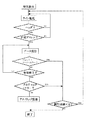
送信側の立体形半導体素子でのフローチャートを図10に示す。データの送信を行う場合、決められた送信プロコトルにより、初期設定を行った後、受信側のアドレスを設定し、データの送信を行う。送信中に信号の衝突が発生したり、あるいは、指定した受信側の装置からアクノリッジが返って来なかったときは再送を行う。動作中は、ラインの状態やアクノリッジの有無について、受信側の記録装置などに設けた表示部上に表示し、ユーザに的確な判断をうながす。
【0101】
受信側の記録装置でのフローチャートを図11に示す。この受信側では、常にライン監視を行い、自分のアドレスを確認したら、ラインからデータを取り込み、メイン・メモリ上のバッファに蓄積していく。受信中に、16バイト毎のブロック・マークが確認出来なかったり、あるいは受信終了後の誤り検出処理でチェックサムが一致しなかった場合は、受信エラーとして、受信を中断し、再度ラインを監視し、ヘッダの到着を待つ。エラー無く受信出来た場合には、表示部上に受信内容を表示する。
【0102】
以上のような実施例の立体形半導体素子は、着脱可能に装着されたインクタンクに収容されたインクをインクジェット記録ヘッドに供給し、その記録ヘッドから噴射するインク滴で記録用紙に印字するインクジェットプリンタに関してのインク情報およびタンク情報を検知し、該インクジェットプリンタに該情報を伝送して、最適な方法でプリンタを制御したり、タンク内の状態を最適維持する制御をするインクジェットプリンタに好ましく適用される。
【0103】
本発明の立体形半導体素子を適用できるインクタンクの構成例を図12〜図15に示す。図12に示すインクタンク501は、インクを収納した可撓性のインク袋502を筐体503内に配置し、筐体503に固定したゴム栓504で袋口502aを閉じておき、インク導出用の中空針505をゴム栓504に突き刺して袋内に連通させることで、不図示のインクジェットヘッドへインク供給を行なうものである。このようなインクタンク501のインク袋502内に本発明の立体形半導体素子506を配置することができる。
【0104】
また、図13に示すインクタンク511は、インク513を収容した筐体512のインク供給口514に、インクを記録紙Sに向けて吐出し記録を行なうインクジェットヘッド515を取付けたものである。このようなタンク511内のインク513中に本発明の立体形半導体素子516を配置することができる。
【0105】
また、図14に示すインクタンク521は、インク522を収容する完全密閉状態の第1室と、負圧発生部材523を収納する大気連通状態の第2室と、タンク最下部で第1室と第2室を連通させる連通路524とを備えたものである。第2室側のインク供給口525よりインクが消費されると、第2室側より大気が第1室へ入ることに替わって第1室のインク522が第2室に導出される。このような構成のタンク521の第1室に本発明の立体形半導体素子526を配し、インクに関する情報をやり取りしてもよい。
【0106】
また、図15に示すインクタンク531は、インクを保持した多孔質部材532を収納し、収納インクを記録のために使用するインクジェットヘッド533を取付けたものである。このような構成のタンク531においても、インクタンク側に本発明の立体形半導体素子534を配し、インクに関する情報をやり取りしてもよい。
【0107】
次に、本発明の立体形半導体素子を備えたインクタンクを搭載するインクジェット記録装置の構成例を図16に概略図で示す。図16に示されるインクジェット記録装置600に搭載されたヘッドカートリッジ601は、印字記録のためにインクを吐出する液体吐出ヘッドと、その液体吐出ヘッドに供給される液体を保持する図12〜図15に示したような構造からなる複数色のインクタンクとを有するものである。また、各色のインクタンク内にそれぞれ配された立体形半導体素子と電磁波で通信を行なう通信回路(図1の符号150)が記録装置600内に設置されている。通信回路の有する共振回路(起電力となるエネルギーの供給部)101はキャリッジ7に設けられていて、各色の立体形半導体素子に電磁波の信号を送信可能となっている。そして、キャリッジ7にヘッドカートリッジ100が装着された状態で、タンク内の素子の発振回路32の導電体コイルLとキャリッジ側の外部共振回路31のコイルLaとが隣接するように設計されている。
【0108】
ヘッドカートリッジ601は、図16に示すように、駆動モータ602の正逆回転に連動して駆動力伝達ギヤ603および604を介して回転するリードスクリュー605の螺旋溝606に対して係合するキャリッジ607上に搭載されている。駆動モータ602の動力によってヘッドカートリッジ601がキャリッジ607ともとにガイド608に沿って矢印aおよびbの方向に往復移動される。インクジェット記録装置600には、ヘッドカートリッジ601から吐出されたインクなどの液体を受ける被記録媒体としてのプリント用紙Pを搬送する被記録媒体搬送手段(不図示)が備えられている。その被記録媒体搬送手段によってプラテン609上を搬送されるプリント用紙Pの紙押さえ板610は、キャリッジ607の移動方向にわたってプリント用紙Pをプラテン609に対して押圧する。
【0109】
リードスクリュー605の一端の近傍には、フォトカプラ611および612が配設されている。フォトカプラ611および612は、キャリッジ607のレバー607aの、フォトカプラ611および612の領域での存在を確認して駆動モータ602の回転方向の切り換えなどを行うためのホームポジション検知手段である。プラテン609の一端の近傍には、ヘッドカートリッジ601の吐出口のある前面を覆うキャップ部材614を支持する支持部材613が備えられている。また、ヘッドカートリッジ601から空吐出などされてキャップ部材614の内部に溜まったインクを吸引するインク吸引手段615が備えられている。このインク吸引手段615によりキャップ部材614の開口部を介してヘッドカートリッジ601の吸引回復が行われる。
【0110】
インクジェット記録装置600には本体支持体619が備えられている。この本体支持体619には移動部材618が、前後方向、すなわちキャリッジ607の移動方向に対して直角な方向に移動可能に支持されている。移動部材618には、クリーニングブレード617が取り付けられている。クリーニングブレード617はこの形態に限らず、他の形態の公知のクリーニングブレードであってもよい。さらに、インク吸引手段615による吸引回復操作にあたって吸引を開始するためのレバー620が備えられており、レバー620は、キャリッジ607と係合するカム621の移動に伴って移動し、駆動モータ602からの駆動力がクラッチ切り換えなどの公知の伝達手段で移動制御される。ヘッドカートリッジ601に設けられた発熱体に信号を付与したり、前述した各機構の駆動制御を司ったりするインクジェット記録制御部は記録装置本体側に設けられており、図15では示されていない。
【0111】
上述した構成を有するインクジェット記録装置600では、前記の被記録媒体搬送手段によりプラテン609上を搬送されるプリント用紙Pに対して、ヘッドカートリッジ601がプリント用紙Pの全幅にわたって往復移動する。この移動時に不図示の駆動信号供給手段からヘッドカートリッジ601に駆動信号が供給されると、この信号に応じて液体吐出ヘッド部から被記録媒体に対してインク(記録液体)が吐出され、記録が行われる。
【0112】
【発明の効果】
本発明の立体形半導体素子によれば、外部からの電磁波の信号が所定の応答条件を満たした場合のみ、周囲環境情報を入手して外部に伝達する通信機能を備えているため、各素子ごとの周囲環境情報が独立して得られる。また、3次元的に情報入手・伝達が可能なので、平板形の半導体素子を用いる場合と比べて、情報伝達の方向の制限も少ない。このため、周囲環境情報の入手、外部への伝達を効率良く行うことができる。
【0113】
また、このような立体形半導体素子をインクタンク内に少なくとも一つ配することで、インクタンク内に収容したインクに関する情報や、タンク内の圧力などをリアルタイムで外部の例えばインクジェット記録装置に伝達させることが可能である。これは、例えばインク消費に伴って時々刻々と変化するタンク内の負圧量を制御してインクジェット吐出を安定化する上で有利である。
【0114】
特に上記の立体形半導体素子を複数のインクタンク内にそれぞれ配置した場合、受信した電磁波の信号が所定の応答条件を満たしたときのみ、受信信号に応じた情報を入手して、蓄積情報との比較判断結果をその入手情報とともに外部へ伝達できるので、応答条件をタンク毎に変えれば、インクタンクごとの情報が独立して得られる。そのため、ユーザーは間違えることなく、たとえばインクが無くなったインクタンクを交換することができる。
【0115】
さらに、立体形半導体素子を動作させるための電力を非接触で供給する構成であるので、素子の起動のための電源をインクタンクに持たせたり、電力供給用の配線を素子に接続する必要がなく、外部との直接的な配線を施すことが困難な箇所に使用することができる。また、非接触で接近した位置で機能するため、一つの位置で複数色を扱うことも可能である。また印字中も伝達可能である。
【0116】
例えば、発振回路の導電体コイルを立体形半導体素子の外表面に巻き付けるように形成することにより、外部の共振回路との間で電磁誘導によって導電体コイルに電力を発生させて、素子に非接触で電力を供給することができる。
【0117】
この場合、素子の外表面にはコイルが巻き付けられているので、そのコイルのインダクタンスの大きさはインクタンク内の例えばインクの残量、インク濃度、インクpHに応じて変化する。したがって、発振回路はそのインダクタンスの変化に応じて発振周波数を変更するので、その変更される発振周波数の変化に基づいてインクタンク内のインクの残量などを検出することも可能である。
【0118】
そして、立体形半導体素子は、液中に浮遊するための空洞部を有するとともに、素子の重心が、当該素子の中心より下部に位置するように形成されているので、例えば、インクジェット記録装置に搭載された記録ヘッドおよびインクタンクが、シリアルに動作し、インクタンク内のインクが上下左右に揺動しても、安定してインクタンク内のインク中に浮遊しながら、インクに関する情報や、タンク内の圧力などを精度良く検出することができる。その上、素子に形成した上記の発振回路のコイルを、外部の共振回路のコイルに対して安定した位置で保持し、常に安定した双方向通信をも可能にする。
【図面の簡単な説明】
【図1】本発明の第1の実施の形態によるインクジェット記録装置を示す概略構成図である。
【図2】本発明の立体形半導体素子の受信兼エネルギー変換手段を構成するために表面に巻き付けられた導体コイルを示す図である。
【図3】本発明の立体形半導体素子の内部構成および外部とのやり取りを表したブロック構成図である。
【図4】本発明の第2の実施の形態によるインクジェット記録装置において装置本体側とタンク内の立体形半導体素子との間で電磁誘導によりディジタルIDをやり取りする概念の説明図である。
【図5】図4に示したディジタルIDのやり取りを用いて特定の色のタンク内情報を入手する動作フローを示す図である。
【図6】本発明の立体形半導体素子の構成要素であるエネルギー発生手段の電力発生原理を説明するための図である。
【図7】本発明の立体形半導体素子の製造方法の一例を説明するための工程図である。
【図8】本発明の立体形半導体素子に使用するN−MOS回路を縦断するように切断した模式的断面図である。
【図9】図7で示す方法で製造した立体形半導体素子が液体中で安定した状態を保持するための条件を説明するための図である。
【図10】本発明の実施例による立体形半導体素子と記録装置とで双方向通信を行なう場合の、送信側の立体形半導体素子でのフローチャートを示す図である。
【図11】本発明の実施例による立体形半導体素子と記録装置とで双方向通信を行なう場合の、受信側の記録装置でのフローチャートを示す図である。
【図12】本発明の立体形半導体素子を適用できるインクタンクの構成例を示す図である。
【図13】本発明の立体形半導体素子を適用できるインクタンクの構成例を示す図である。
【図14】本発明の立体形半導体素子を適用できるインクタンクの構成例を示す図である。
【図15】本発明の立体形半導体素子を適用できるインクタンクの構成例を示す図である。
【図16】本発明の立体形半導体素子を備えたインクタンクを搭載するインクジェット記録装置の構成例を示す概略図である。
【図17】特開平6−143607号に記載のインク残量検知装置を示す図である。
【図18】特登録2947245号に記載のインク残量検知装置を示す図である。
【符号の説明】
11、210 立体形半導体素子
12 電磁波
13 電力
14 受信兼エネルギー変換手段
15 情報入手手段
16 判断手段
17 情報蓄積手段
18 情報伝達手段
101 外部共振回路
102 発振回路
150 通信回路
151 誘導コイル
152 周波数変調器
201 球状シリコン
202 SiO2膜
203 開口
204 空洞部
205 SiN膜
206 Cu膜
207 封止部材[0001]
BACKGROUND OF THE INVENTION
The present invention relates to a semiconductor device having a function of detecting surrounding environmental information, transmitting the information to the outside, and displaying the information.
[0002]
The present invention also provides a device for detecting information (for example, remaining ink amount) in each color ink tank and displaying and transmitting the information to the outside, an ink tank equipped with the device, and a facsimile / mountable ink tank equipped with the ink tank. The present invention relates to an ink jet recording apparatus such as a printer / copier.
[0003]
[Prior art]
2. Description of the Related Art Conventionally, in an ink jet recording apparatus in which an image is printed on a paper in a dot pattern by moving a carriage mounted with a recording head in a printing direction while ejecting ink from a plurality of ejection nozzles provided in the recording head. An ink tank containing recording ink is provided, and the ink in the ink tank is supplied to the recording head via the ink supply path. In view of this, various proposals have been made that an ink remaining amount detection device that detects the remaining amount of ink in the ink tank is put to practical use.
[0004]
For example, according to Japanese Patent Laid-Open No. 6-143607, two (one pair)
[0005]
According to Japanese Patent Registration No. 2947245, as shown in FIG. 18, the lower part is formed in a funnel shape toward the bottom surface, and two conductors 801 and 802 are provided on the bottom surface, and the specific gravity is smaller than that of the ink 803. An ink cartridge 805 for an ink jet printer having a configuration in which a metal ball 804 is installed is disclosed. In such a configuration, when the ink 803 is consumed and decreased, the liquid level of the ink 803 is lowered. Along with this, the position of the metal sphere 804 floating on the surface of the ink 803 is lowered. When the liquid level of the ink 803 is lowered to the position of the bottom surface of the ink cartridge housing, the metal ball 804 comes into contact with the two conductors 801 and 802. Then, since the conductors 801 and 802 become conductive, a current flows between them. If the flow is detected, the ink end state can be detected. If the ink end state is detected, information indicating the ink end state is notified to the user.
[0006]
[Problems to be solved by the invention]
A configuration for detecting the remaining amount of ink in the ink tank as represented by the above-described conventional publication is known. However, in such a configuration, it is necessary to dispose a detection electrode in the ink tank. In addition, since the ink remaining amount is detected based on the conductive state between the electrodes, there are restrictions on the ink to be used, such as metal ions not being used for the ink component.
[0007]
In the above configuration, only the remaining amount of ink can be detected, and other information in the tank cannot be known from the outside. For example, pressure information in the ink tank, changes in ink physical properties, etc. are important parameters for operating the inkjet head at a stable discharge amount, and the tank pressure that changes from time to time as the ink in the tank is consumed. There is a demand for a tank that can notify an external ink jet recording apparatus in real time and transmit changes in ink physical properties to the outside.
[0008]
Furthermore, there is a demand for an ink tank that not only unilaterally informs the detected information in the ink tank to the outside but also allows bidirectional exchange of information such as returning internal information in response to an external inquiry. .
[0009]
In developing the ink tank as described above, the present inventors paid attention to Ball Semiconductor Co., Ltd., which forms a semiconductor integrated circuit on a spherical surface of a silicon ball having a diameter of 1 mm. Since this ball semiconductor has a spherical shape, if it is housed in an ink tank, it is expected that the detection of ambient environment information and the exchange of bidirectional information with the outside can be performed much more efficiently than the flat type. . However, as a result of investigating those having such functions, it is necessary to develop an element itself having the above-mentioned functions only by the technology of connecting the ball semiconductors with electric wiring as in US Pat. No. 5,877,943. It was. In addition, there is a problem that must be cleared for this element to be effectively applicable to an ink tank. One of the problems is the supply of electric power for starting the elements accommodated in the tank. If the ink tank has a power source for starting the element, the tank will become large, or even if a power source is provided outside the tank, a means for connecting the power source and the element will be required, increasing the tank manufacturing cost, and the tank cartridge However, the device must be activated without contact from the outside.
[0010]
As a further problem, it is possible to float in the ink liquid level of the ink tank or in the ink that has sunk a certain distance from the liquid level. For example, it is desirable that the element is located on the ink surface to monitor the fluctuation of the negative pressure amount due to the ink consumption in the ink tank over time. However, since the element is made of silicon having a specific gravity higher than that of water, it floats on the ink. It is difficult to do.
[0011]
In particular, when applied to a color printer, a tank capable of acquiring and transmitting in-tank information in response to an external inquiry is required for each color tank.
[0012]
An object of the present invention is to detect a detailed information in each color ink tank in real time and to exchange information bidirectionally with an external ink jet recording apparatus, and an ink including the semiconductor element It is to provide a tank and an ink jet recording apparatus.
[0013]
[Means for Solving the Problems]
In order to achieve the above object, the present invention includes a plurality of ink jet heads for performing color recording with an ink jet printer, and includes a plurality of ink tanks for storing ink ejected corresponding to each ink jet head. In an inkjet recording system that performs
Each saidInk tankWithinThree-dimensional semiconductor elementArranged on the surface of the ink liquid or suspended in the liquidAnd inkjet printersWireless communication is performed by electromagnetic waves with the three-dimensional semiconductor element arranged in each ink tank outside the ink tank.Communication means are provided,
Each of the three-dimensional semiconductor elements is the communication means.RadenMagnetic waveReceiving the signal in a contactless manner,Electromagnetic waveBy electromagnetic inductionConvert to electricityReceiver with coilEnergy conversion means;Information on at least the remaining amount of ink in the ink tank in which the solid-state semiconductor element is arranged that is activated by the electric power is obtained.Equipped with information acquisition means, information storage means, judgment means and information transmission meansAnd
For each of the three-dimensional semiconductor elements, the resonance frequency is different by changing the number of turns or the length of the coil,
By the communication means,A signal with a frequency equal to the resonance frequency of a given three-dimensional semiconductor deviceIs electromagnetic wavesSent byWhen,ConcernedSolid semiconductor elementChild reception cumEnergy conversion meansBy electromagnetic inductionTo powerconversiondo it, The information acquisition means, the information storage means, the judgment means and the information transmission means by the powerStart
Corresponding to the predetermined resonance frequencySolid semiconductor elementOnlyThree-dimensional semiconductor element by means of information acquisitionAt least information on the remaining ink in the ink tankobtainAndThat informationSaidBy means of judgmentSaidWhen it is necessary to transmit information by comparing with the information stored in the information meansSaidTransmit to the outside of the ink tank by information transmission meansRukoIt is characterized by.
The present invention also provides an ink jet recording system that includes a plurality of ink jet heads for performing color recording with an ink jet printer, and has a plurality of ink tanks for storing ink ejected corresponding to each ink jet head for recording. In
In each ink tank, the solid semiconductor element is arranged in a state of floating on the surface of the ink liquid or in the liquid, and the ink jet printer has a solid form arranged in the ink tank in addition to the ink tank. Communication means for performing wireless communication with semiconductor elements by electromagnetic waves is provided,
Each of the three-dimensional semiconductor elements receives a signal of electromagnetic waves from the communication means in a non-contact manner, and receives and energy conversion means having a coil for converting the electromagnetic waves into electric power by electromagnetic induction, and is activated by the electric power, An information acquisition means, information storage means, determination means, and information transmission means for obtaining at least information on the remaining amount of ink in the ink tank in which the three-dimensional semiconductor element is arranged, and different identification for each of the three-dimensional semiconductor elements Have an ID,
When a signal including an identification ID of a predetermined three-dimensional semiconductor element is transmitted as an electromagnetic wave by the communication means, the reception and energy conversion means of each of the three-dimensional semiconductor elements converts the electromagnetic wave into electric power by electromagnetic induction, The information acquisition means, the information storage means, the judgment means and the information transmission means are activated by the power,
Only the solid semiconductor element having the identification ID that matches the identification ID transmitted from the communication means accepts information following the identification ID from the communication means, and according to the received information, the information obtaining means When information of at least the remaining amount of ink in the ink tank in which the solid semiconductor element is arranged is obtained, and the obtained information is compared with the information of the accumulated information means by the judging means to transmit information. The information is transmitted to the outside of the ink tank by the information transmitting means.
[0015]
The response condition is characterized by different digital ID identification.
[0018]
Moreover, what has the cavity part for floating at the liquid surface or the predetermined position in a liquid is preferable. In this case, it is preferable that the three-dimensional semiconductor element floating in the liquid has a center of gravity located below the center of the element and does not rotate in the floating liquid and stably swings. More preferably, the metacenter of the element is always above the center of gravity of the solid semiconductor element.
[0026]
The “metacenter” in the present specification indicates the intersection of the action line of weight when balanced and the action line of buoyancy when tilted.
[0027]
Further, the “three-dimensional shape” of the “three-dimensional semiconductor element” in this specification includes all three-dimensional shapes such as a triangular prism, a sphere, a hemisphere, a quadrangular prism, a spheroid, and a uniaxial rotator.
[0028]
When used in an ink jet recording apparatus, means for supplying an electromagnetic wave signal to the element may be provided at a recovery position, a return position, a carriage, a head, or the like. In addition to this, if an apparatus having means for supplying an electromagnetic wave signal is used, the state inside the ink tank can be known without an ink jet recording apparatus. For example, if used in a factory or a store, it can be used for inspection or the like. (quality assurance).
[0029]
(Function)
In the three-dimensional semiconductor element as described above, when an electromagnetic wave signal satisfying a predetermined response condition is provided from the outside of the element without contact, the energy conversion means converts the electromagnetic wave into electric power, and the converted electric power The information acquisition means, determination means, information storage means, and information transmission means are activated. When the electromagnetic wave signal received by the energy conversion means satisfies a predetermined response condition, environmental information around the element is obtained by the information obtaining means, and the obtained information and the information stored in the information accumulation means corresponding thereto are obtained. Are judged by the judging means to judge the necessity of information transmission. When it is determined that information transmission is necessary, the determination unit transmits the acquired information to the outside by the information transmission unit.
[0030]
In this way, only when the signal of the electromagnetic wave from the outside satisfies a predetermined response condition, a communication function for obtaining ambient environment information and transmitting it to the outside is built in the three-dimensional semiconductor element. Ambient environment information can be obtained independently. In addition, since information can be obtained and transmitted three-dimensionally, there are fewer restrictions on the direction of information transmission compared to the case of using a flat semiconductor element. For this reason, acquisition of ambient environment information and transmission to the outside can be performed efficiently.
[0031]
the aboveBy disposing at least one of the three-dimensional semiconductor elements in the ink tank, it is possible to transmit information on the ink stored in the ink tank, the pressure in the tank, and the like to an external inkjet recording apparatus in real time. Is possible. This is advantageous, for example, in stabilizing the inkjet discharge by controlling the amount of negative pressure in the tank that changes every moment as the ink is consumed.
[0032]
In particular, the above three-dimensional semiconductor elements are respectively arranged in a plurality of ink tanks.ForOnly when the received electromagnetic wave signal satisfies a predetermined response condition, information corresponding to the received signal can be obtained and the result of comparison with the stored information can be transmitted to the outside together with the obtained information. If it changes every time, the information for every ink tank can be obtained independently. Therefore, the user can replace, for example, an ink tank that has run out of ink without making a mistake.
[0033]
Furthermore, since the power for operating the three-dimensional semiconductor element is supplied in a non-contact manner, it is necessary to provide the ink tank with a power source for starting the element or to connect a power supply wiring to the element. And can be used in places where it is difficult to perform direct wiring with the outside.
[0034]
For example, by forming the conductor coil of the oscillation circuit around the outer surface of the three-dimensional semiconductor element, electric power is generated in the conductor coil by electromagnetic induction with the external resonance circuit, and the element is not contacted. Can supply power.
[0035]
In this case, since a coil is wound around the outer surface of the element, the magnitude of the inductance of the coil varies depending on, for example, the remaining amount of ink, ink concentration, and ink pH in the ink tank. Therefore, since the oscillation circuit changes the oscillation frequency in accordance with the change in inductance, it is possible to detect the remaining amount of ink in the ink tank based on the change in the changed oscillation frequency.
[0036]
The three-dimensional semiconductor element has a cavity for floating in the liquid and is formed so that the center of gravity of the element is located below the center of the element. Even if the recording head and the ink tank are operated serially and the ink in the ink tank swings up and down, left and right, the ink is stably floating in the ink in the ink tank. Can be detected with high accuracy. In addition, the coil of the oscillation circuit formed on the element is held at a stable position with respect to the coil of the external resonance circuit, and stable bi-directional communication is always possible.
[0037]
DETAILED DESCRIPTION OF THE INVENTION
Hereinafter, embodiments of the present invention will be described with reference to the drawings. In particular, an embodiment in which a three-dimensional semiconductor element is arranged in each color ink tank will be described in detail. It should be noted that this element is not housed only in the ink tank, but the same effect can be obtained even if it is used in another object.
[0038]
(First embodiment)
FIG. 1 is a schematic configuration diagram showing an ink jet recording apparatus according to a first embodiment of the present invention. The ink jet recording apparatus 600 of the form shown in this figure includes a liquid discharge head (not shown) that discharges ink droplets for printing and an ink tank 500 of each color that holds the liquid supplied to the liquid discharge head. A carriage 607 to be mounted is provided. As the ink tanks 500 for the respective colors, four types of color tanks of black B, cyan C, magenta M, and yellow Y are mounted.
[0039]
Each color ink tank is provided with a three-dimensional semiconductor element 11 having a communication function with different response conditions, and can communicate with a
[0040]
The
[0041]
In addition, since the three-dimensional semiconductor element 11 includes the induction coil L, the electromagnetic induction by the resonance circuit 102 of the
[0042]
In the ink jet recording apparatus as described above, for example, when information is exchanged with a cyan tank, a signal having a frequency equal to the resonance frequency corresponding to the cyan color is transmitted from the
[0043]
FIG. 3 is a block diagram showing the internal configuration of the three-dimensional semiconductor element 11 arranged for each color and the exchange with the outside.
[0044]
The three-dimensional semiconductor element 11 receives a signal of the electromagnetic wave 12 sent from the
[0045]
The judging means 16 accepts the signal of the electromagnetic wave 12 when the receiving / energy converting means (oscillation circuit having a coil) 14 resonates with the received electromagnetic wave 12, and does not accept it when it does not resonate. When the signal of the electromagnetic wave 12 is received, the
[0046]
The
[0047]
According to this embodiment, since the three-dimensional semiconductor element having a communication function that responds at different frequencies is arranged in each color ink tank, information can be exchanged individually with the tank of the desired color.
[0048]
In addition, the solid-state semiconductor element for each color converts the electromagnetic wave from the communication circuit provided on the recording apparatus main body side into electric power for starting the determination means, the information acquisition means, the information transmission means, etc. in the element. Thus, the element can be used at any location in the object, such as in ink, where it is difficult to perform direct electrical wiring externally. If an element is arranged in the ink, the state of the ink can be accurately grasped in real time. Furthermore, since it is not necessary to arrange a means (power source in this example) for accumulating an electromotive force for operating the element, the element can be miniaturized and the element can be used even in a narrow place.
[0049]
(Second Embodiment)
Next, another embodiment will be described. The basic configuration of the three-dimensional semiconductor element is the same as that shown in FIG. 3, but the response conditions in communication are different. Therefore, in the description, the same reference numerals are used for the same components as those in the first embodiment. In the case of this embodiment, the frequency to be tuned for communication is the same for all the elements in the ink tank of each color unlike the first embodiment (determined by the number of turns and the length of the coil L on the element). The resonance frequency is the same for each color element), but each element arranged in each color tank has a different digital ID identification function, and the tank of the color to be communicated is identified by the digital ID to allow communication. Judge whether to disable or not.
[0050]
FIG. 4 is an explanatory diagram of a concept of exchanging a digital ID by electromagnetic induction between the
[0051]
FIG. 4 shows an operation flow for obtaining in-tank information of a specific color by using such exchange of digital IDs. Referring to this figure, when the ID of the response condition of the ink tank to be communicated is selected (in this case, the digital ID is D3h), the
[0052]
Then, the judging means 16 compares the obtained hexadecimal ID with the hexadecimal identification ID stored in the information storage means 17 in advance. If the comparison matches, the information following the ID is accepted, and if the comparison does not match, it is not accepted.
[0053]
When the information is received as described above, as shown in FIG. 3, the
[0054]
According to this embodiment, since the three-dimensional semiconductor element having a communication function that responds with a communication protocol using different ID identifications is arranged in each color ink tank, the desired color is the same as in the first embodiment. Information can be exchanged individually with the tank, and power can be supplied in a non-contact manner to activate the circuit in the element, so that it can be used even in inks where wiring is difficult.
[0055]
Furthermore, in the present embodiment, by identifying the ink tanks of the respective colors based on the digital ID, it becomes possible to handle a much larger number of tanks than the configuration of the first embodiment.
[0056]
【Example】
Next, a preferred specific example in which the three-dimensional semiconductor element of the present invention is arranged in an ink tank will be described in more detail.
[0057]
First, information acquisition means applicable to the three-dimensional semiconductor element of the present invention will be described as an example. As described in the above embodiment, when a three-dimensional semiconductor element is arranged in an ink tank, information acquisition means built into spherical silicon can be (1) SiO.2A sensor that detects the pH of the ink by creating a film or SiN film as an ion-sensitive film, (2) a pressure sensor that has a diaphragm structure and detects pressure changes in the tank, and (3) converts light into thermal energy Then, a photodiode with a pyroelectric effect is built in to detect the current position, and a sensor for detecting the remaining amount of ink, and (4) the presence or absence of ink depending on the amount of moisture in the tank using the conductive effect of the material. Examples include a sensor to detect.
[0058]
Next, specific examples of receiving and energy converting means applicable to the three-dimensional semiconductor device of the present invention will be given. FIG. 6 is a diagram for explaining the principle of power generation of the reception and energy conversion means that is a component of the three-dimensional semiconductor element of the present invention.
[0059]
In FIG. 6, when the conductor coil L of the oscillation circuit 102 is placed adjacent to the coil La of the external resonance circuit 101 and a current Ia is passed through the coil La through the external resonance circuit 101, the coil I of the oscillation circuit 102 is caused by the current Ia. Is generated. Here, when the current Ia is changed, the magnetic flux B penetrating the coil L is changed, so that an induced electromotive force V is generated in the coil L. Therefore, the oscillation circuit 102 as the reception and energy conversion means is formed in the spherical silicon, the external resonance circuit 101 is provided in the
[0060]
Further, the magnetic flux B penetrating through the coil L having the winding number N of the oscillation circuit 102 formed in spherical silicon as a receiving and energy conversion means is proportional to the product of the winding number Na of the coil La of the external resonance circuit 101 and the current Ia. , Where the proportionality constant is k
[0061]
[Expression 1]
B = k * Na * Ia (1)
The electromotive force V generated in the coil L is
[0062]
[Expression 2]
[0063]
[Equation 3]
[0064]
Mutual inductance of equation (2): M is
[0065]
[Expression 4]
[0066]
And the impedance of the oscillation circuit built in spherical silicon: Z is
[0067]
[Equation 5]
Z (ω) = R + j {ωL− (1 / ωC)} (5)
The impedance of the external resonant circuit: Za is
[0068]
[Formula 6]
Za (ω) = Ra + jωLa− {ω2M2/ Z (ω)} (6)
It becomes. Here, J represents magnetization. And the impedance: Zo when this external resonance circuit resonates (when the current value: Ia becomes maximum) is:
[0069]
[Expression 7]
Zo (ωo) = Ra + jLaωo− (ωo 2M2/ R) ▲ 7 ▼
The phase delay of this resonant circuit: φ is
[0070]
[Equation 8]
tanφ = {jLaωo− (ωo 2M2/ R)} / R (8)
It becomes.
[0071]
The resonance frequency fo of this external resonance circuit is
[0072]
[Equation 9]
fo = 1 / 2π (LC)1/2 ▲ 9 ▼
Is required.
[0073]
From the above relationship, when the impedance of the oscillation circuit 102 built in the spherical silicon is varied according to the change of the ink in the ink tank, the frequency of the external resonance circuit 101 is changed to change the impedance of the external resonance circuit 101. The change in the ink appears in the amplitude and phase difference. Further, the remaining amount of ink (that is, change in z) is included in the phase difference and amplitude.
[0074]
For example, by changing the resonance frequency of the external resonance circuit 101, the output (impedance) from the oscillation circuit 102 built in the spherical silicon changes according to changes in the surrounding environment, so this frequency dependency is detected. By doing so, it is possible to detect the presence or absence of ink and the remaining ink amount.
[0075]
Therefore, the oscillation circuit built in the spherical silicon is not only used as an energy generating means for generating electric power, but also as a part of means for detecting a change in ink in the tank due to the relationship between the oscillation circuit and the external resonance circuit. It is possible to use.
[0076]
Next, the manufacturing method of the three-dimensional semiconductor element of this invention is demonstrated. FIG. 7 is a process diagram for explaining an example of the manufacturing method of the three-dimensional semiconductor element of the present invention, and shows each process by a cross section passing through the center of the spherical silicon. Here, an example is given of a manufacturing method in which the center of gravity of the spherical silicon is formed so as to be lower than the center, the upper part inside the spherical body is made hollow, and the hollow part is kept airtight.
[0077]
The spherical silicon shown in FIG. 7 (a) is thermally oxidized on the entire surface as shown in FIG. 7 (b).2After forming the
[0078]
Then, as shown in FIG. 7D, only the upper silicon portion is removed by anisotropic etching using a KOH solution through the
[0079]
Further, as shown in FIG. 7F, a
[0080]
Further, an N-MOS circuit is used as a drive circuit element other than the coil L formed in such a floating three-dimensional semiconductor element. FIG. 8 shows a schematic cross-sectional view of the N-MOS circuit cut in a longitudinal direction.
[0081]
According to FIG. 8, P-
[0082]
The element driving N-
[0083]
Here, when the N-
[0084]
Between the elements, an oxide
[0085]
After each element is formed, an interlayer insulating film 416 is deposited with a thickness of about 7000 angstrom by a PSG film, a BPSG film, etc. by a CVD method, and planarized by a heat treatment, and then the first through a contact hole. Wiring is performed by an
[0086]
And the connection with the oscillation circuit as a receiving and energy conversion means of this invention, the sensor part as an information acquisition means, etc. is performed through the said through hole.
[0087]
Further, in any state of the ink tank provided with the floating solid semiconductor element of this example, the oscillation circuit built in the spherical silicon by the above-described manufacturing method and the external resonance circuit shown in FIG. A stable magnetic flux (magnetic field) must be working between However, when floating in a liquid such as ink, the liquid level may vibrate due to external vibration. Even in such a case, in this example, the center of gravity of the floating three-dimensional semiconductor element is determined in order to maintain a stable state in the liquid.
[0088]
As shown in FIG. 9, when the three-
(1) Buoyancy F = weight W of the object
(2) The buoyancy action line and the weight action line (the line passing through the center of gravity G) match.
It is necessary that this relationship holds.
[0089]
Then, as shown in FIG. 9B, when the liquid vibrates due to the external force and the three-
[0090]
Here, the intersection of the action line of weight when in a balanced state (one-dot chain line in FIG. 9B) and the action line of buoyancy when tilted (solid line in FIG. 9B) is defined as the metacenter. The distance h between the metacenter and the center of gravity is called the height of the metacenter.
[0091]
Since the metacenter of the three-
[0092]
[Expression 10]
[0093]
Therefore, in order to make this restoring force positive, it is a necessary and sufficient condition that h> 0.
[0094]
From FIG. 9B,
[0095]
## EQU11 ##
[0096]
[Expression 12]
[0097]
As a bidirectional communication method with external communication means at this time, a wireless LAN system using a microwave band frequency or a wireless access system using a quasi-millimeter wave / millimeter wave frequency can be applied.
[0098]
Here, an outline of transmission and reception by the wireless LAN system will be described. In the following, data transmission from the three-dimensional semiconductor element to the recording apparatus will be described. On the contrary, when data is transmitted from the recording apparatus side to the three-dimensional semiconductor element, a data ID is arranged on each side, and the data ID is identified.
[0099]
The three-dimensional semiconductor element on the transmission side has a line monitoring unit, a data handling unit, an acknowledge check unit, and an error processing unit, and the recording device on the reception side has a data handling unit, an acknowledge unit, and an error processing unit. And a display part etc. are attached.
[0100]
A flowchart of the three-dimensional semiconductor element on the transmission side is shown in FIG. In the case of data transmission, initial setting is performed using a predetermined transmission protocol, and then the address on the receiving side is set and data transmission is performed. If a signal collision occurs during transmission, or if no acknowledgment is returned from the designated receiving device, retransmission is performed. During operation, the line status and the presence / absence of an acknowledge are displayed on a display unit provided in a recording apparatus on the receiving side, and the user is appropriately judged.
[0101]
FIG. 11 shows a flowchart in the receiving side recording apparatus. On this receiving side, line monitoring is always carried out, and when its own address is confirmed, data is fetched from the line and stored in a buffer on the main memory. During reception, if the block mark for every 16 bytes cannot be confirmed, or if the checksum does not match in the error detection process after reception, the reception is interrupted and the line is monitored again. Wait for the header to arrive. If it can be received without error, the received content is displayed on the display unit.
[0102]
The three-dimensional semiconductor element of the embodiment as described above is an ink jet printer that supplies ink contained in an ink tank that is detachably mounted to an ink jet recording head, and prints on recording paper with ink droplets ejected from the recording head. The present invention is preferably applied to an ink jet printer that detects ink information and tank information about the ink and transmits the information to the ink jet printer to control the printer in an optimal manner or to control the state in the tank optimally. .
[0103]
12 to 15 show configuration examples of ink tanks to which the three-dimensional semiconductor element of the present invention can be applied. In the ink tank 501 shown in FIG. 12, a flexible ink bag 502 containing ink is disposed in a
[0104]
In addition, an ink tank 511 shown in FIG. 13 has an ink jet head 515 attached to an ink supply port 514 of a casing 512 that accommodates ink 513 to eject ink toward the recording paper S and perform recording. The three-dimensional semiconductor element 516 of the present invention can be disposed in the ink 513 in such a tank 511.
[0105]
In addition, the ink tank 521 shown in FIG. 14 includes a first chamber in a completely sealed state that stores the
[0106]
Further, an ink tank 531 shown in FIG. 15 is a container in which a porous member 532 holding ink is stored and an ink jet head 533 that uses the stored ink for recording is attached. Also in the tank 531 having such a configuration, the three-dimensional semiconductor element 534 of the present invention may be arranged on the ink tank side to exchange information about ink.
[0107]
Next, a configuration example of an ink jet recording apparatus equipped with an ink tank provided with the three-dimensional semiconductor element of the present invention is schematically shown in FIG. A head cartridge 601 mounted on the inkjet recording apparatus 600 shown in FIG. 16 holds a liquid discharge head that discharges ink for print recording, and holds liquid supplied to the liquid discharge head in FIGS. A plurality of color ink tanks having the structure as shown. In addition, a communication circuit (
[0108]
As shown in FIG. 16, the head cartridge 601 is engaged with a helical groove 606 of a
[0109]
Photocouplers 611 and 612 are disposed near one end of the
[0110]
The ink jet recording apparatus 600 includes a main body support 619. A moving member 618 is supported on the main body support 619 so as to be movable in the front-rear direction, that is, in a direction perpendicular to the moving direction of the carriage 607. A cleaning blade 617 is attached to the moving member 618. The cleaning blade 617 is not limited to this form, and may be a known cleaning blade of another form. Further, a lever 620 for starting suction is provided in the suction recovery operation by the ink suction means 615, and the lever 620 moves in accordance with the movement of the cam 621 that engages with the carriage 607, and from the drive motor 602. The driving force is controlled to move by known transmission means such as clutch switching. An ink jet recording control unit that provides a signal to a heating element provided in the head cartridge 601 and controls driving of each mechanism described above is provided on the recording apparatus main body side and is not shown in FIG. .
[0111]
In the ink jet recording apparatus 600 having the above-described configuration, the head cartridge 601 reciprocates over the entire width of the print paper P with respect to the print paper P transported on the platen 609 by the recording medium transport means. When a drive signal is supplied from the drive signal supply means (not shown) to the head cartridge 601 during this movement, ink (recording liquid) is discharged from the liquid discharge head portion to the recording medium in accordance with this signal, and recording is performed. Done.
[0112]
【The invention's effect】
According to the three-dimensional semiconductor element of the present invention, each element has a communication function for obtaining ambient environment information and transmitting it to the outside only when an external electromagnetic wave signal satisfies a predetermined response condition. The surrounding environment information can be obtained independently. In addition, since information can be obtained and transmitted three-dimensionally, there are fewer restrictions on the direction of information transmission compared to the case of using a flat semiconductor element. For this reason, acquisition of ambient environment information and transmission to the outside can be performed efficiently.
[0113]
In addition, by disposing at least one such three-dimensional semiconductor element in the ink tank, information on the ink stored in the ink tank, the pressure in the tank, and the like are transmitted to an external inkjet recording apparatus in real time. It is possible. This is advantageous, for example, in stabilizing the inkjet discharge by controlling the amount of negative pressure in the tank that changes every moment as the ink is consumed.
[0114]
In particular, when each of the above three-dimensional semiconductor elements is arranged in a plurality of ink tanks, only when the received electromagnetic wave signal satisfies a predetermined response condition, information corresponding to the received signal is obtained and stored information is stored. Since the comparison judgment result can be transmitted to the outside together with the obtained information, if the response condition is changed for each tank, the information for each ink tank can be obtained independently. Therefore, the user can replace, for example, an ink tank that has run out of ink without making a mistake.
[0115]
Furthermore, since the power for operating the three-dimensional semiconductor element is supplied in a non-contact manner, it is necessary to provide the ink tank with a power source for starting the element or to connect a power supply wiring to the element. And can be used in places where it is difficult to perform direct wiring with the outside. Moreover, since it functions at a close position without contact, it is possible to handle a plurality of colors at one position. It can also be transmitted during printing.
[0116]
For example, by forming the conductor coil of the oscillation circuit around the outer surface of the three-dimensional semiconductor element, electric power is generated in the conductor coil by electromagnetic induction with the external resonance circuit, and the element is not contacted. Can supply power.
[0117]
In this case, since a coil is wound around the outer surface of the element, the magnitude of the inductance of the coil varies depending on, for example, the remaining amount of ink, ink concentration, and ink pH in the ink tank. Therefore, since the oscillation circuit changes the oscillation frequency in accordance with the change in inductance, it is possible to detect the remaining amount of ink in the ink tank based on the change in the changed oscillation frequency.
[0118]
The three-dimensional semiconductor element has a cavity for floating in the liquid and is formed so that the center of gravity of the element is located below the center of the element. Even if the recording head and the ink tank are operated serially and the ink in the ink tank swings up and down, left and right, the ink is stably floating in the ink in the ink tank. Can be detected with high accuracy. In addition, the coil of the oscillation circuit formed on the element is held at a stable position with respect to the coil of the external resonance circuit, and stable bi-directional communication is always possible.
[Brief description of the drawings]
FIG. 1 is a schematic configuration diagram showing an ink jet recording apparatus according to a first embodiment of the present invention.
FIG. 2 is a view showing a conductor coil wound around a surface in order to constitute a receiving and energy converting means of a three-dimensional semiconductor element of the present invention.
FIG. 3 is a block diagram showing the internal configuration of the three-dimensional semiconductor device of the present invention and the exchange with the outside.
FIG. 4 is an explanatory view of a concept of exchanging a digital ID by electromagnetic induction between the apparatus main body side and a three-dimensional semiconductor element in a tank in an ink jet recording apparatus according to a second embodiment of the present invention.
5 is a diagram showing an operation flow for obtaining in-tank information of a specific color using the exchange of the digital ID shown in FIG. 4. FIG.
FIG. 6 is a diagram for explaining the principle of power generation of energy generating means that is a constituent element of the three-dimensional semiconductor element of the present invention.
FIG. 7 is a process diagram for explaining an example of a method for manufacturing a three-dimensional semiconductor element of the present invention.
FIG. 8 is a schematic cross-sectional view of the N-MOS circuit used in the three-dimensional semiconductor element of the present invention cut in a longitudinal direction.
FIG. 9 is a view for explaining conditions for maintaining a stable state in a liquid for a three-dimensional semiconductor device manufactured by the method shown in FIG. 7;
FIG. 10 is a diagram illustrating a flowchart of a three-dimensional semiconductor element on the transmission side when two-dimensional communication is performed between the three-dimensional semiconductor element and a recording apparatus according to an embodiment of the present invention.
FIG. 11 is a diagram showing a flowchart in the recording apparatus on the receiving side when bidirectional communication is performed between the solid semiconductor element and the recording apparatus according to the embodiment of the present invention.
FIG. 12 is a diagram showing a configuration example of an ink tank to which the three-dimensional semiconductor element of the present invention can be applied.
FIG. 13 is a diagram showing a configuration example of an ink tank to which the three-dimensional semiconductor element of the present invention can be applied.
FIG. 14 is a diagram showing a configuration example of an ink tank to which the three-dimensional semiconductor element of the present invention can be applied.
FIG. 15 is a diagram showing a configuration example of an ink tank to which the three-dimensional semiconductor element of the present invention can be applied.
FIG. 16 is a schematic view showing a configuration example of an ink jet recording apparatus equipped with an ink tank provided with the three-dimensional semiconductor element of the present invention.
FIG. 17 is a diagram showing an ink remaining amount detecting device described in Japanese Patent Laid-Open No. 6-143607.
FIG. 18 is a diagram showing an ink remaining amount detecting device described in Japanese Patent No. 2947245;
[Explanation of symbols]
11, 210 Three-dimensional semiconductor element
12 Electromagnetic waves
13 Electric power
14 Receiving and energy conversion means
15 Information acquisition means
16 Judgment means
17 Information storage means
18 Information transmission means
101 External resonant circuit
102 Oscillator circuit
150 Communication circuit
151 induction coil
152 frequency modulator
201 spherical silicon
202 SiO2film
203 opening
204 Cavity
205 SiN film
206 Cu film
207 Sealing member
Claims (3)
それぞれの前記インクタンク内において立体形半導体素子がインク液体表面もしくは液中に浮遊した状態で配されているとともに、インクジェットプリンタには前記インクタンクの外に、それぞれの前記インクタンク内に配された立体形半導体素子と電磁波で無線通信を行う通信手段が設けられており、
それぞれの前記立体形半導体素子は、前記通信手段から電磁波の信号を非接触で受信し、該電磁波を電磁誘導により電力に変換するコイルを有する受信兼エネルギー変換手段と、該電力により起動する、前記立体形半導体素子が配されているインクタンク内の少なくともインク残量の情報を入手する情報入手手段と情報蓄積手段と判断手段と情報伝達手段を備え、かつ、
前記立体形半導体素子ごとに、前記コイルの巻き数あるいは長さを変えることで共振周波数が異なっており、
前記通信手段により、所定の立体形半導体素子の共振周波数に等しい周波数の信号が電磁波で送られると、当該立体形半導体素子の受信兼エネルギー変換手段が該電磁波を電磁誘導により電力に変換して、該電力により前記情報入手手段、前記情報蓄積手段、前記判断手段および前記情報伝達手段を起動し、
前記所定の共振周波数に対応した立体形半導体素子のみが、前記情報入手手段によってその立体形半導体素子が配されているインクタンク内の少なくともインク残量の情報を入手し、その入手した情報を前記判断手段によって前記蓄積情報手段の情報と比較判断して情報伝達が必要な場合に前記情報伝達手段によりインクタンク外部に伝達することを特徴とするインクジェット記録システム。In an ink jet recording system comprising a plurality of ink jet heads for performing color recording with an ink jet printer and mounting a plurality of ink tanks for storing ink ejected corresponding to each ink jet head.
Together are distributing in the state in which three-dimensional type semiconductor device is suspended in the ink liquid surface or submerged in each of the ink tank, the ink jet printer outside the ink tank, arranged in each of the ink tank Communication means for wireless communication with a three-dimensional semiconductor element by electromagnetic waves is provided,
Each of the three dimensional semiconductor device receives a signal of the communication means or al electromagnetic wave without contact, and receiving and energy conversion means having a coil that converts the electromagnetic wave into power by electromagnetic induction is activated by said power , e Bei information acquiring means and information storage means and determination means and the information transmission means for obtaining information of at least the amount of ink remaining in the ink tank, wherein the solid type semiconductor device is disposed, and,
For each of the three-dimensional semiconductor elements, the resonance frequency is different by changing the number of turns or the length of the coil,
By the communication means, the frequency signal equal to the resonance frequency of the predetermined solid type semiconductor device is sent at the electromagnetic wave, received and energy conversion means of the three dimensional semiconductor element is to convert the electromagnetic wave into power by electromagnetic induction The information acquisition means, the information storage means, the judgment means and the information transmission means are activated by the power,
Only three dimensional semiconductor device corresponding to the predetermined resonant frequency, the information acquiring means by to obtain information of at least the remaining amount of ink in the ink tank to which the solid type semiconductor device is disposed, said the information received an ink jet recording system comprising a Turkey be transmitted to the ink tank outside by the information transmitting means when the storage information means information comparison determining and signaling is required for the determination means.
それぞれの前記インクタンク内において立体形半導体素子がインク液体表面もしくは液中に浮遊した状態で配されているとともに、インクジェットプリンタには前記インクタンクの外に、前記インクタンク内に配された立体形半導体素子と電磁波で無線通信を行う通信手段が設けられており、In each ink tank, the solid semiconductor element is arranged in a state of floating on the surface of the ink liquid or in the liquid, and the ink jet printer has a solid form arranged in the ink tank in addition to the ink tank. Communication means for performing wireless communication with semiconductor elements by electromagnetic waves is provided,
それぞれの前記立体形半導体素子は、前記通信手段から電磁波の信号を非接触で受信し、該電磁波を電磁誘導により電力に変換するコイルを有する受信兼エネルギー変換手段と、該電力により起動する、前記立体形半導体素子が配されているインクタンク内の少なくともインク残量の情報を入手する情報入手手段と情報蓄積手段と判断手段と情報伝達手段を備え、かつ、前記立体形半導体素子ごとに異なる識別IDを持ち、Each of the three-dimensional semiconductor elements receives a signal of electromagnetic waves from the communication means in a non-contact manner, and receives and energy conversion means having a coil for converting the electromagnetic waves into electric power by electromagnetic induction, and is activated by the electric power, An information acquisition means, information storage means, determination means, and information transmission means for obtaining at least information on the remaining amount of ink in the ink tank in which the three-dimensional semiconductor element is arranged, and different identification for each of the three-dimensional semiconductor elements Have an ID,
前記通信手段により、所定の立体形半導体素子の識別IDを含む信号が電磁波で送られると、それぞれの前記立体形半導体素子の受信兼エネルギー変換手段が該電磁波を電磁誘導により電力に変換して、該電力により前記情報入手手段、前記情報蓄積手段、前記判断手段および前記情報伝達手段を起動し、When a signal including an identification ID of a predetermined three-dimensional semiconductor element is transmitted as an electromagnetic wave by the communication means, the reception and energy conversion means of each of the three-dimensional semiconductor elements converts the electromagnetic wave into electric power by electromagnetic induction, The information acquisition means, the information storage means, the judgment means and the information transmission means are activated by the power,
前記通信手段から送信された識別IDと一致した識別IDを持つ立体形半導体素子のみが、前記通信手段からの識別IDの後に続く情報を受け入れ、この受け入れた情報に応じて前記情報入手手段により、その立体形半導体素子が配されているインクタンク内の少なくともインク残量の情報を入手し、その入手した情報を前記判断手段によって前記蓄積情報手段の情報と比較判断して情報伝達が必要な場合に前記情報伝達手段によりインクタンク外部に伝達することを特徴とするインクジェット記録システム。Only the solid semiconductor element having the identification ID that matches the identification ID transmitted from the communication means accepts information following the identification ID from the communication means, and according to the received information, the information obtaining means When information of at least the remaining amount of ink in the ink tank in which the solid semiconductor element is arranged is obtained, and the obtained information is compared with the information of the accumulated information means by the judging means to transmit information. An ink jet recording system wherein the information is transmitted to the outside of the ink tank by the information transmitting means.
Priority Applications (20)
| Application Number | Priority Date | Filing Date | Title |
|---|---|---|---|
| JP2000181839A JP3814465B2 (en) | 2000-06-16 | 2000-06-16 | Inkjet recording system |
| EP06115291A EP1710084B1 (en) | 2000-06-16 | 2001-06-13 | Solid semiconductor element, ink tank, ink jet recording apparatus provided with ink tank, and associated method of use |
| EP08161261A EP1990201B1 (en) | 2000-06-16 | 2001-06-13 | Communication system with solid semiconductor element, ink tank, ink jet recording apparatus provided with ink tank. |
| AT08161261T ATE468227T1 (en) | 2000-06-16 | 2001-06-13 | COMMUNICATION SYSTEM WITH SOLID STATE SEMICONDUCTOR COMPONENT, INK TANK, INK JET RECORDING DEVICE EQUIPPED WITH SUCH INK TANK. |
| US09/878,946 US6827411B2 (en) | 2000-06-16 | 2001-06-13 | Solid semiconductor element, ink tank, ink jet recording apparatus provided with ink tank, liquid information acquiring method and liquid physical property change discriminating method |
| AT01114377T ATE402821T1 (en) | 2000-06-16 | 2001-06-13 | INKJET RECORDING DEVICE USING A SOLID STATE SEMICONDUCTOR DEVICE |
| DE60135064T DE60135064D1 (en) | 2000-06-16 | 2001-06-13 | An ink jet recording apparatus using a solid state semiconductor device |
| DE60136304T DE60136304D1 (en) | 2000-06-16 | 2001-06-13 | Solid state semiconductor device, ink tank, ink jet recording device equipped with this ink tank and method of use |
| EP01114377A EP1164022B1 (en) | 2000-06-16 | 2001-06-13 | Ink jet recording apparatus utilizing solid semiconductor element |
| DE60142198T DE60142198D1 (en) | 2000-06-16 | 2001-06-13 | Communication system with solid state semiconductor device, ink tank, ink jet recording device equipped with this ink tank. |
| CA002350397A CA2350397C (en) | 2000-06-16 | 2001-06-13 | Solid semiconductor element, ink tank, ink jet recording apparatus provided with ink tank, liquid information acquiring method and liquid physical property change discriminating method |
| AT06115291T ATE411900T1 (en) | 2000-06-16 | 2001-06-13 | SOLID STATE SEMICONDUCTOR COMPONENT, INK TANK, INKJET RECORDING APPARATUS EQUIPPED WITH SUCH INK TANK AND METHOD OF USE |
| SG200103511A SG109453A1 (en) | 2000-06-16 | 2001-06-14 | Solid semiconductor element, ink tank, ink jet recording apparatus provided with ink tank, liquid information acquiring method and liquid physical property change discriminating method |
| SG200404745A SG127735A1 (en) | 2000-06-16 | 2001-06-14 | Solid semiconductor element, ink tank, ink jet recording apparatus provided with ink tank, liquid information acquiring method and liquid physical property change discriminating method |
| TW090114637A TW514964B (en) | 2000-06-16 | 2001-06-15 | Solid semiconductor element, ink tank, ink jet recording apparatus provided with ink tank, liquid information acquiring method and liquid physical property change discriminating method |
| CNB011412844A CN100457463C (en) | 2000-06-16 | 2001-06-15 | Ink jet recording apparatus |
| KR10-2001-0034162A KR100427203B1 (en) | 2000-06-16 | 2001-06-16 | Solid semiconductor element, ink tank, ink jet recording apparatus provided with ink tank, liquid information acquiring method and liquid physical property change discriminating method |
| US10/127,594 US7014287B2 (en) | 2000-06-16 | 2002-04-23 | Solid semiconductor element, ink tank, ink jet recording apparatus provided with ink tank, liquid information acquiring method and liquid physical property change discriminating method |
| US10/646,700 US7210755B2 (en) | 2000-06-16 | 2003-08-25 | Solid semiconductor element, ink tank, ink jet recording apparatus provided with ink tank, liquid information acquiring method and liquid physical property change discriminating method |
| US11/707,055 US7922274B2 (en) | 2000-06-16 | 2007-02-16 | Solid semiconductor element, ink tank, ink jet recording apparatus provided with ink tank, liquid information acquiring method and liquid physical property change discriminating method |
Applications Claiming Priority (1)
| Application Number | Priority Date | Filing Date | Title |
|---|---|---|---|
| JP2000181839A JP3814465B2 (en) | 2000-06-16 | 2000-06-16 | Inkjet recording system |
Publications (2)
| Publication Number | Publication Date |
|---|---|
| JP2002005724A JP2002005724A (en) | 2002-01-09 |
| JP3814465B2 true JP3814465B2 (en) | 2006-08-30 |
Family
ID=18682705
Family Applications (1)
| Application Number | Title | Priority Date | Filing Date |
|---|---|---|---|
| JP2000181839A Expired - Fee Related JP3814465B2 (en) | 2000-06-16 | 2000-06-16 | Inkjet recording system |
Country Status (1)
| Country | Link |
|---|---|
| JP (1) | JP3814465B2 (en) |
Families Citing this family (12)
| Publication number | Priority date | Publication date | Assignee | Title |
|---|---|---|---|---|
| JP2004205660A (en) * | 2002-12-24 | 2004-07-22 | Oki Data Corp | Consumable cartridge and image forming apparatus |
| JP4337383B2 (en) | 2003-04-10 | 2009-09-30 | セイコーエプソン株式会社 | Equipment capable of mounting consumable containers |
| US7192107B2 (en) | 2003-04-21 | 2007-03-20 | Seiko Epson Corporation | Information communicating member, liquid container having information communicating member and liquid ejecting apparatus |
| JP4298629B2 (en) | 2003-12-26 | 2009-07-22 | キヤノン株式会社 | Inkjet recording device |
| MXPA04012681A (en) | 2003-12-26 | 2005-07-01 | Canon Kk | Liquid container and liquid supplying system. |
| JP4058434B2 (en) | 2003-12-26 | 2008-03-12 | キヤノン株式会社 | Ink storage container, method for manufacturing the same, and printer system |
| JP4898147B2 (en) * | 2005-06-01 | 2012-03-14 | キヤノン株式会社 | Ink tank |
| JP4821371B2 (en) * | 2006-03-03 | 2011-11-24 | セイコーエプソン株式会社 | Ink cartridge, ink information control system, and electronic device |
| JP4898926B2 (en) * | 2010-01-07 | 2012-03-21 | キヤノン株式会社 | Inkjet recording device |
| US8801161B2 (en) | 2011-07-27 | 2014-08-12 | Brother Kogyo Kabushiki Kaisha | Liquid cartridge, image recording device, and substrate |
| CN102896902B (en) * | 2011-07-28 | 2015-04-01 | 兄弟工业株式会社 | Liquid box and image recording device |
| JP5095004B2 (en) * | 2011-10-24 | 2012-12-12 | キヤノン株式会社 | Ink storage container and ink jet recording apparatus including ink storage container |
-
2000
- 2000-06-16 JP JP2000181839A patent/JP3814465B2/en not_active Expired - Fee Related
Also Published As
| Publication number | Publication date |
|---|---|
| JP2002005724A (en) | 2002-01-09 |
Similar Documents
| Publication | Publication Date | Title |
|---|---|---|
| CA2350402C (en) | Ink tank and ink jet recording apparatus provided with the same | |
| EP1164023B1 (en) | Ink jet recording apparatus utilizing solid semiconductor element | |
| CN100364775C (en) | Solid semiconductor element, ink cartridge with same, and method of their use | |
| CN100457463C (en) | Ink jet recording apparatus | |
| JP3814465B2 (en) | Inkjet recording system | |
| JP3745199B2 (en) | Ink tank provided with three-dimensional semiconductor element, and ink jet recording apparatus equipped with the ink tank | |
| JP3610281B2 (en) | Ink tank | |
| JP3610286B2 (en) | Ink tank | |
| JP3610296B2 (en) | Liquid storage container | |
| JP3605003B2 (en) | Ink jet recording apparatus and ink information collecting method | |
| JP3495973B2 (en) | Communication method, ink tank, recording device, and communication system | |
| JP2001358292A (en) | Three-dimensional semiconductor element, ink tank in which the element is arranged, and ink jet recording apparatus having the tank |
Legal Events
| Date | Code | Title | Description |
|---|---|---|---|
| A977 | Report on retrieval |
Free format text: JAPANESE INTERMEDIATE CODE: A971007 Effective date: 20040715 |
|
| A131 | Notification of reasons for refusal |
Free format text: JAPANESE INTERMEDIATE CODE: A131 Effective date: 20040728 |
|
| A521 | Written amendment |
Free format text: JAPANESE INTERMEDIATE CODE: A523 Effective date: 20040922 |
|
| RD03 | Notification of appointment of power of attorney |
Free format text: JAPANESE INTERMEDIATE CODE: A7423 Effective date: 20040922 |
|
| A02 | Decision of refusal |
Free format text: JAPANESE INTERMEDIATE CODE: A02 Effective date: 20051122 |
|
| A521 | Written amendment |
Free format text: JAPANESE INTERMEDIATE CODE: A523 Effective date: 20051220 |
|
| A911 | Transfer of reconsideration by examiner before appeal (zenchi) |
Free format text: JAPANESE INTERMEDIATE CODE: A911 Effective date: 20060203 |
|
| A131 | Notification of reasons for refusal |
Free format text: JAPANESE INTERMEDIATE CODE: A131 Effective date: 20060405 |
|
| A521 | Written amendment |
Free format text: JAPANESE INTERMEDIATE CODE: A523 Effective date: 20060417 |
|
| TRDD | Decision of grant or rejection written | ||
| A01 | Written decision to grant a patent or to grant a registration (utility model) |
Free format text: JAPANESE INTERMEDIATE CODE: A01 Effective date: 20060517 |
|
| A61 | First payment of annual fees (during grant procedure) |
Free format text: JAPANESE INTERMEDIATE CODE: A61 Effective date: 20060605 |
|
| R150 | Certificate of patent or registration of utility model |
Free format text: JAPANESE INTERMEDIATE CODE: R150 |
|
| FPAY | Renewal fee payment (event date is renewal date of database) |
Free format text: PAYMENT UNTIL: 20090609 Year of fee payment: 3 |
|
| FPAY | Renewal fee payment (event date is renewal date of database) |
Free format text: PAYMENT UNTIL: 20100609 Year of fee payment: 4 |
|
| FPAY | Renewal fee payment (event date is renewal date of database) |
Free format text: PAYMENT UNTIL: 20110609 Year of fee payment: 5 |
|
| LAPS | Cancellation because of no payment of annual fees |