JP3794185B2 - Device using photoconductive switching element, device incorporating the device, recording apparatus and recording method - Google Patents
Device using photoconductive switching element, device incorporating the device, recording apparatus and recording method Download PDFInfo
- Publication number
- JP3794185B2 JP3794185B2 JP01219399A JP1219399A JP3794185B2 JP 3794185 B2 JP3794185 B2 JP 3794185B2 JP 01219399 A JP01219399 A JP 01219399A JP 1219399 A JP1219399 A JP 1219399A JP 3794185 B2 JP3794185 B2 JP 3794185B2
- Authority
- JP
- Japan
- Prior art keywords
- pulse
- switching element
- charge generation
- photoconductive switching
- liquid crystal
- Prior art date
- Legal status (The legal status is an assumption and is not a legal conclusion. Google has not performed a legal analysis and makes no representation as to the accuracy of the status listed.)
- Expired - Fee Related
Links
Images


Landscapes
- Liquid Crystal (AREA)
- Optical Modulation, Optical Deflection, Nonlinear Optics, Optical Demodulation, Optical Logic Elements (AREA)
Description
【0001】
【発明の属する技術分野】
本発明は、有機光導電体を用いた光スイッチング素子、それを用いたデバイス、装置、記録装置、および記録方法に関する
【0002】
【従来の技術】
近年、光導電スイッチング素子と表示素子等の機能素子を組み合わせた光書き込み型空間変調デバイスが開発され、ライトバルブとしてプロジェクター等に実用化されているほか、" 液晶空間変調器と情報処理" 液晶, Vol.2,No.1, '98, pp3-18 にあるように、光情報処理の分野にも可能性が検討されている。
光書き込み型空間変調デバイスは、所定の電圧を素子に印加しつつ、受光した光量により光導電性スイッチング素子のインピーダンスを変化させ、表示素子に印加される電圧を制御することにより、表示素子を駆動し、画像を表示するものである。
【0003】
これらの、受光した光量により電圧あるいは電流を制御できるような素子としては、例えば、CCD に用いられるフォトダイオードや密着型イメージセンサに用いられるa-Si、それに電子写真用感材に用いられる有機光導電体などが研究開発されている。特に有機光導電体(OPC) は、暗時の電流が小さく、また、安価な材料コスト、製造が容易なことによる高い生産性により、電子写真用感材や太陽電池に実用化されているが、同様の理由に基づき有機光導電体を光導電スイッチング素子へ適用することが期待されている。
【0004】
従来、電子写真用感材として提案され実用化されているOPC は、一般的には図27のような構造である。すなわち導電性基板50の表面にOPC を電荷発生層51(CGL) と電荷輸送層52(CTL) の2 層構造にして、表面にイオンをチャージする、この後、光を照射すると、OPC が光スイッチング素子となり、光が照射された部分はイオンチャージが消され、光が照射されない部分はチャージが残る。光が照射された部分のイオンチャージが消されるメカニズムは以下のとおりである。すなわち、電荷発生層51は光を受けると、その波長、光量により、層内でキャリアと電子を生じ、電荷を生成する。発生した電子またはキャリアは、電荷輸送層52を通じて表面まで移動し、表面のイオンによる電荷を打ち消す。これにより光を照射された部分は電荷が消滅し、光が照射されていない部分は電荷が残留する。この後、帯電したトナーを電荷が残留した部位に付着させた後、トナーを紙に転写・ 定着し、印字画像を得る。ここで電荷輸送層が必要な理由は、電荷発生層は耐圧が低いためである。光スイッチとしてのOPC の耐圧を高めるために電荷輸送層を具備する必要がある。
また、太陽電池に適用されている構造は例えば図28に示されるように、透明基板60にAlのごとき半透明な導電膜61、たとえばSiO やZnO などn 型の無機光導電層62、X型無金属フタロシアニンのようなp型の有機光導電層63と、電極64を順次積層した構造を有している。これにフォトンが入射することによりn 型層とp 型層の界面に電位差が生じることを利用するものである。この場合には高い耐圧は必要なく、したがって電荷輸送層は必要ない。
【0005】
しかしながら、有機光導電体スイッチング素子は以下のような問題があった。すなわち、整流作用があることである。通常、電荷輸送層による輸送は電子またはキャリアのどちらか一方である。なぜなら、電荷輸送層材料は電子吸引性か電子供与性材料が使われるためである。もちろん、ポリビニルカルバゾールのように両極性の輸送が可能なものもあるが、感度に問題があり、ほとんど実用化されていない。
このため、有機光導電体をたとえば、液晶素子と組み合わせた画像表示装置あるいは、応用物理学会編" 光情報処理"pp171にあるような光書き込み型空間変調素子などには適用できなかった。その理由は、以下に述べるように印加電圧が高圧化し、それに伴って画像の焼き付きが発生するからである。すなわち、整流作用をもつOPC に電圧印加する場合、正負両極性での電圧印加は困難であるため、液晶に電界が実効的に加えられる時間が減少することになってしまう。したがって、液晶の配向制御を行うためには、より高い電圧を印加するか、あるいはより長い時間の電圧印加が必要となる。
【0006】
また、整流作用のため、一方の極性の電界印加が困難であることから実効的に直流のバイアスが液晶に加えられることと等価であるため、そのバイアスにより液晶内イオンが電極近傍に移動し、そのイオンの発生する電界によりスイッチングが困難になり、画像焼き付きが発生してしまう。したがって、通常、液晶内のイオンの移動による画像の焼き付きを防ぐために正負の交流電界が印加される。
液晶に限らず、実効的に直流バイアス成分がかかってはいけない素子のスイッチングには従来構造のOPC を使用することは困難である。
このため、例えば、液晶を用いた光スイッチング方式の画像表示装置には、H.Yoshida,T.Takizawaら"Reflective Display with Photoconductive Layer and a Bistable, Reflective Cholesteric Mixture" SID‘96 APPLICATIONS DIGEST pp59 等に光導電スイッチング素子としてa-Siが使われている。a-Siは両極での電荷発生および輸送が可能であるが、高度な膜形成手段が必要であり、作製プロセスは一般的にプラズマCVD が用いられるが、通常200 度以上に基板を加熱する必要がありためプラスチック基板への適用が困難であるほか、生産コストが高くなり、工程管理も厳しく、現在は実用化されていない。また、a-Siの代わりにSeやCdS などの光感光体も考えられるが、これらはいずれも環境および人体に非常に有害な材料である。
【0007】
【発明が解決しようとする課題】
本発明は、上記の問題点を解決するためになされたものであり、その目的は、交流電界または交流電流によって駆動される機能素子と高機能で安価な光導電スイッチング素子を電気的に接続したデバイスを提供することであり、さらに光導電スイッチング素子と液晶表示素子などの機能素子を一体化したデバイス、前記デバイスを組み込んだ装置、記録装置、ならびに記録方法をも提供することにある。
【0008】
【課題を解決するための手段】
上記目的は、以下の光導電スイッチング素子、デバイス、装置、記録装置および記録方法を提供することにより解決される。
(1) 交流電界あるいは交流電流により駆動される機能素子と、前記機能素子と電気的に接続される前記機能素子のスイッチングを行うための光導電スイッチング素子とを備え、前記機能素子を駆動する交流電界あるいは交流電流は、前記光導電スイッチング素子への光照射下で前記機能素子に印加されるデバイスであって、
前記光導電スイッチング素子が、光透過性の基板上に少なくとも、前記交流電界あるいは交流電流が印加される光透過性の電極層、有機電荷発生材料により構成される電荷発生層、有機電荷輸送材料により構成される電荷輸送層、および有機電荷発生材料により構成される電荷発生層を順次積層することにより構成されることを特徴とするデバイス。(以下において、前記電荷発生層および電荷輸送層を単に「電荷発生層」、「電荷輸送層」という。)
本発明に用いる光導電スイッチング素子は、電荷輸送層を挟んで二層の電荷発生層を形成しているため、交流電界を印加した場合0Vを中心とした対称性が極めて優れている。
また、前記電荷発生層と電荷輸送層の境界において、電荷発生材料と電荷輸送材料が混合され、かつ混合比が各層の積層方向に連続的に変化している光導電スイッチング素子を有利に挙げることができる。また、前記基板としてプラスチック基板を用いることがより有利である。また、前記電荷発生層および電荷輸送層を構成する材料として有機材料を有利に用いることができる。
【0009】
(2)上記(1) に記載の光導電スイッチング素子と機能素子を一体化したデバイス。
機能素子が、メモリ性のある機能素子、表示素子、メモリ性のある表示素子、液晶表示素子、メモリ性のある液晶表示素子、コレステリック液晶表示素子の場合、本発明のデバイスは、効果的にその機能を発揮する。
光導電スイッチング素子と機能素子とを一体化させることにより光導電スイッチング素子と機能素子の接続を安定化させることができる。特に、メモリ性を有する機能素子と光導電スイッチング素子とを一体化させたデバイスは、デバイスを駆動する本体から分離させることが可能で、分離させたデバイスを配布したりすることができる。
(3) 上記(1) に記載の光導電スイッチング素子、直流成分除去用機能膜、および機能素子例えば表示素子を順次積層し一体化したデバイス。
本発明のデバイスにおいて直流成分除去用機能膜を設けたことにより、上記0Vを中心とした対称性が一層向上する。
直流成分除去用機能膜が、表示素子部よりも大きな容量成分を有することにより、より効果的にその性能を発揮する。
また、直流成分除去用機能膜を構成する材料が、ポリビニルアルコール(PVA) 、ポリビニルカルバゾール、ポリ酢酸ビニル、ポリエチレンオキシド、ポリブチルアルコールからなる群より選択される有機材料か、あるいは、Si-O、Ti-O、Al-O、Si-N、PZT 、Ta-O、Al-Nからなる群より選択される無機材料を主成分とすることにより、より効率的にその性能を発揮する。
【0010】
(4) 上記 (1)に記載の光導電スイッチング素子とメモリ性のある機能素子、表示素子、メモリ性のある表示素子、液晶表示素子、メモリ性のある液晶表示素子あるいはコレステリック液晶表示素子を一体化したデバイス、該デバイスと電気的に接続されデバイスを駆動する駆動機構を有する装置であって、該駆動機構は該デバイスと切り離し可能であることを特徴とする装置。
前記デバイスは、光導電スイッチング素子と一体化させた機能素子又は各表示素子に、光導電スイッチング素子への光照射下で交流電界あるいは交流電流が印加され駆動されるものである。
この装置は、光導電スイッチング素子と前記のごとき機能素子を一体化したデバイスと、これと切り離し可能な駆動機構を有しているため、デバイスとデバイスを駆動する本体とを分離させることが可能で、分離させたデバイスを配布したりすることができる。
(5) 上記(3) に記載のデバイスと、該デバイスと電気的に接続されデバイスを駆動する駆動機構とを有する装置であって、該駆動機構は該デバイスと切り離し可能であることを特徴とする装置。
【0011】
(6) 上記(1) に記載の光導電スイッチング素子および表示素子を一体化させたデバイスと、光導電スイッチング素子に光を入射する光書き込み手段と、該デバイスを駆動するために駆動パルスとして正極性パルスと負極性パルスを該デバイスに入力するパルス入力手段とを有する記録装置。
前記デバイスは、前記表示素子に、光導電スイッチング素子への光照射下で正極性パルスと負極性パルスが印加されるものである。
この記録装置は上記(1) の光導電スイッチング素子を使用しているため、交流電界駆動を行った場合に高い反射率が得られる。
【0012】
(7) 前記記録装置のパルス入力手段としては、最終パルスとして負極性のパルスを入力するか、第一パルスとして正極性パルスを入力するか、あるいは第一パルスとして正極性パルスをまた最終パルスとして負極性パルスを入力するパルス入力手段であることが好ましい。ここで負極性パルスとは、デバイスの光導電スイッチング素子側の電極よりも、表示素子側の電極の方が高電位になるように印加されるパルスを意味する。また、正極性パルスとは、デバイスの光導電スイッチング素子側の電極の方が、表示素子側の電極よりも高電位になるように印加されるパルスを意味する。また、この記録装置においてデバイスがさらに直流成分除去用機能膜を備えていることが好ましい。また、この記録装置において、表示素子としてコレステリック液晶表示素子を用い、かつパルス印加手段として、最終パルスに負極性パルスを入力する(第一パルスの極性のいかんは問わない。)パルス入力手段を用いる記録装置が好ましい。
(8) 上記(7) に記載の記録装置を使用する記録方法であって、前記デバイスを駆動するために駆動パルスとして正極性パルスと負極性パルスを該デバイスに入力するとともに、光導電スイッチング素子に光を入射して光書き込みを行い、かつ最終パルスとして負極性パルスを入力するか、第一パルスとして正極性パルスを入力するか、あるいは第一パルスとして正極性パルスをまた最終パルスとして負極性パルスを入力することを特徴とする記録方法。
上記(7) および(8) の記録装置および記録方法において、最終パルスとして負極性のパルスを入力する(第一パルスの極性のいかんは問わない。)ことにより、コレステリック液晶表示素子のごとく、電圧オフ時に急峻な電圧降下を必要とする表示素子を使用する場合において、効果的に表示素子をオンにすることができる。
また、上記(7) および(8) の記録装置および記録方法のように、第一パルスとして正極性のパルスを入力することにより、光導電スイッチング素子や表示素子の持つ時定数による影響を排しモデュレーション効果が得られる。
【0013】
【発明の実施の形態】
本発明のデバイスに用いる光導電スイッチング素子は、基本的には光透過性の基板、光透過性の電極層、下部電荷発生層、電荷輸送層および上部電荷発生層から構成されるものであり、電荷輸送層を挟んで2つの電荷発生層を有することを特徴としている。(なお、以下においては「光透過性」という性質を「透明」と表現することがある。)
図1を用いて、本発明の光導電スイッチング素子を説明する。図1は本発明の光導電スイッチング素子(デュアルCGL 構造の有機光導電スイッチング素子)の構造、及び光導電スイッチング素子に光が照射された際に発生するキャリアおよび電子を示している。図中、10は上部電荷発生層(top CGL) 、12は電荷輸送層、14は下部電荷発生層(tail CGL)、18は光透過性の電極層、および19は光透過性の基板をそれぞれ示し、本発明の光導電スイッチング素子は基本的にはこれらの要素からなっている。また、16は本発明の光導電スイッチング素子の上部電荷発生層の上に形成された電極層を示す。
光照射時、上部電荷発生層10および下部電荷発生層14にキャリアおよび自由電子が発生し、その際上記電極層16が正極、電極層18が負極となるように電界が印加されていると、上部電荷発生層10に発生したキャリアは電荷輸送層12に注入されると同時に自由電子は電極18に突入する。輸送されたキャリアは下部電荷発生層14で発生した電子と結合するとともに下部電荷発生層に生じたキャリアは電極16に注入される。この結果電流が流れる。電界が反転したときは逆方向に流れる。したがって、この構造の光導電スイッチング素子は交流電界あるいは交流電流により駆動することができる。
【0014】
また、本発明の光導電スイッチング素子において、前記電荷発生層と電荷輸送層の境界において、電荷発生材料と電荷輸送材料が混合され、かつ混合比が各層の積層方向に連続的に変化している光導電スイッチング素子は、電荷発生層と電荷輸送層との間の密着力が増し、信頼性の高い光導電スイッチング素子が得られる。上記の混合比を連続的に変化させるとは、例えば上下の電荷発生層の材料の組成M、電荷輸送層の組成をM’とした場合、光導電スイッチング素子の層構造が以下のようになることを意味する。
下部電荷発生層 M/下部境界層 x M−(1−x)M’/電荷輸送層 M’/上部境界層 (1−y)M’+yM/上部電荷発生層 M
ただし、1>x>0、1>y>0であり、下部境界層では下部電荷発生層から電荷輸送層に向かってxが1から0の方向に変化し、また上部境界層では電荷輸送層から上部電荷発生層に向かってyは0から1の方向に変化する。
このように、電荷発生材料、電荷輸送材料の組成が連続的に変わるため、電荷発生層と電荷輸送層との間の密着力が増す。
【0015】
以下に、本発明の光導電スイッチング素子の各層の構成について順次説明する。
まず、本発明の光導電スイッチング素子に用いられる光透過性の基板としては、ガラス、PET(ポリエチレンテレフタレート)、PC(ポリカーボネート)、ポリエチレン、ポリスチレン、ポリイミド、PES(ポリエーテルスルホン)等の、基板が用いられる。フレキシブル基板が得られること、成形が容易なこと、コストの点などから光透過性のプラスチック基板を用いることが有利である。また、本発明における光透過性の電極層としては、ITO膜、Au、SnO2 、Al、Cu等が用いられる。
【0016】
次に、本発明の光導電スイッチング素子の上部電荷発生層および下部電荷発生層に使用する材料について説明する。電荷発生層を構成する材料としては、ペリレン系、フタロシアニン系、ビスアゾ系、ジチオピトケロピロール系、スクワリリウム系、アズレニウム系、チアピリリウム・ ポリカーボネート系など光照射により電荷が発生する有機材料を有利に用いることができる。
上部電荷発生層(10)と下部電荷発生層(14)はキャリアと自由電子の発生が同程度生じることが必要であるため、波長、光量、電圧に対し同程度の感度が必要であり、上下とも同じ材料であることが望ましいが、同程度の感度であるなら材料が異なっていても問題ない。上部と下部の電荷発生材料の感度が同程度でないものを用いて光導電スイッチング素子を構成すると、光照射下交流電界を印加した場合、後で詳述する、取り出される電圧の波形の0Vに対する非対称性が極めて大きくなってしまう。
電荷発生層の作製方法としては、真空蒸着法やスパッタ法などドライな膜形成法のほか、溶液あるいは分散液を用いるスピンコート法、ディップ法などが適用可能である。いづれの方式も、a-Siやフォトダイオード作製におけるような基板加熱や厳しい工程管理は不要である。
上部および下部電荷発生層の膜厚は、10nm〜1 μm、好ましくは20nm〜500nm が適切である。10nmより薄いと光感度が不足しかつ均一な膜の作製が難しくなり、また、1 μmより厚くなると、光感度は飽和し、膜内応力によって剥離が生じ易くなる。
【0017】
電荷輸送層を構成する電荷輸送材料としては、トリニトロフルオレン系、ポリビニルカルバゾール系、オキサジアゾール系、ピラリゾン系、ヒドラゾン系、スチルベン系、トリフェニルアミン系、トリフェニルメタン系、ジアミン系などが適用可能である。また、LiClO4を添加したポリビニルアルコ−ルやポリエチレンオキシドのようなイオン導電性材料の適用も可能である。中でも、ジアミン系が感度、キャリア輸送能力などの点から好ましく用いられる。
電荷輸送層の作製方法としては、真空蒸着法やスパッタ法などドライな膜形成法のほか、溶液あるいは分散液を用いるスピンコート法、ディップ法などが適用可能である。
電荷輸送層の膜厚は、0.1 μm〜100 μm、好ましくは1 μm〜10μmが適切である。0.1 μmより薄いと耐電圧が低くなって信頼性確保が困難となり、また、100 μmより厚くなると、機能素子とのインピーダンスマッチングが困難となって設計が難しくなるため、前記の範囲が望ましい。
【0018】
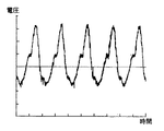
実施例においても詳述するが、ここで図を用いて、本発明の光導電スイッチング素子が電圧対称性に優れていることを説明する。図2は透明な基板に透明な電極層を設け、その上に下部電荷発生層、電荷輸送層、および上部電荷発生層を順次設けた、本発明の光導電スイッチング素子に電極を形成し、前記2つの電極を抵抗を介して接続し、光照射下交流サイン波を印加した場合、抵抗の両端に現れる電圧を観察したものである。一方、図3は、図2の光導電スイッチング素子から上部電荷発生層を除いた構造の光導電スイッチング素子を用いて同様に電圧の変化を調べたものである。図2および図3から明らかなように0Vを中心とした電圧の対称性は、本発明の光導電スイッチング素子が従来の光導電スイッチング素子に比較して極めて優れていることが分かる。
【0019】
電圧の対称性に劣る光導電スイッチング素子を、例えば表示素子を駆動するスイッチング素子として使用した場合、光照射時表示素子に対し、一方の極性においては十分な電圧印加がなされても、反対極性においては十分な電圧印加が得られず、結果として、所望の表示画像が得られなくなる。
例えば、高反射率を得るために、表示素子としての液晶素子に閾値電圧以上を印加した時、一方の極性で十分な電圧印加が行われ高反射率化しても、極性反転後十分な電圧が得られず、液晶が低反射率化してしまい所定の高反射率が得られなくなる。また、閾値特性、すなわち、印加電圧に対する反射率変化の急峻性が劣化してしまうこともある。この場合、例えば、書き込み時に画像のエッジににじみ等が発生して解像度を劣化させる。また、実効的に直流バイアスが印加された状態と同等であり、例えば液晶ではイオンが一方の極性に引かれることになり結果として書き換え困難になる" 画像の焼き付き" が発生してしまう。
この問題を回避するため、例えば、表示素子に対する電圧印加が両極性ともに十分になるように、表示素子により高い電圧を印加することが考えられるが、この場合、すでに十分な電圧印加がなされた極性において、より一層高い電圧が印加されることになり、耐圧の観点から、デバイスの信頼性が下がるほか、消費電力も増えてしまう。
【0020】
このように、従来の光導電スイッチング素子に比較して電荷発生層を2層設けた本発明の光導電スイッチング素子の電圧の対称性は極めて優れているが、上部電荷発生層と下部電荷発生層に全く同じ材料を用いても、光照射下交流電界を印加した場合、取り出される電圧は必ずしも全く対称にはならない。すなわち、上部と下部の電荷発生層に同じ電荷発生材料を用いても同一の光導電特性とはならない。図4には光を照射しない条件で交流電界を印加した場合に取り出される電圧の変化が示されているが、この場合には、非対称性は生じていない。一方、図6は光照射下交流電界を印加した場合に、正極性と負極性において、取り出される電圧(例えば表示素子に印加される電圧)が正負の極性に対し非対称になることを示している。
【0021】
上記のようなデュアルCGL 構造を有する光導電スイッチング素子に電圧の非対称性が生じる理由は以下のように推察される。即ち、たとえば電荷輸送層の上下に電荷発生層を作製するデュアルCGL 構造の場合、光入射側即ち基板側に作製された電荷発生層に比べ、反対側の電荷発生層は光吸収量が、低くなることが挙げられる。光入射後、基板側の電荷発生層に吸収された分減少した光が反対側の電荷発生層に達することになるため、基板側の電荷発生層の光吸収量と反対側の電荷発生層の光吸収量が異なり、非対称性が発生すると考えられる。また、この他に、通常光入射基板上の透明電極上に作製した電荷発生層、あるいは、透明電極上に機能膜としての接着層を介して作製した電荷発生層に比べ、電荷輸送層上に形成した電荷発生層は光感度が低下すると考えられる。
したがって、後述するように、本発明の光導電スイッチング素子に機能素子例えば表示素子を積層してデバイスを構成すると、上記の理由により、電荷は光入射側から機能素子側に流れやすく、逆に機能素子側から基板側に流れにくい。すなわち、光入射側の電極が機能素子側の電極より高電位に変化する場合、電流はより光入射側から機能素子側へ流れやすく、光導電スイッチングの抵抗はより下がる。逆に、機能素子側の電極が光入射側の電極よりも高電位に変化する場合でも、電流は機能素子側から光入射側へ流れにくく、光導電スイッチング素子の抵抗が大きくなる。
【0022】
本発明は、上記の光導電スイッチング素子の電荷輸送層の上下に形成された電荷発生層の光導電特性が同一でない場合、直流成分除去可能な容量成分をもつ機能膜、すなわち直流成分除去用機能膜を光導電スイッチング素子に設けることが実効的な直流バイアスを除去するのに有効であり、上記の電圧対称性を改善することを見いだした。以下に直流成分除去用機能膜について詳述する。
直流成分除去用機能膜の特性である容量性の交流電圧印加時の効果を観察する目的で以下のような評価実験を行った。
液晶表示部を有するデバイスにおいては各機能性部材毎の波形測定が事実上困難であるため、下記のようにして実験セルを作製した。
まず、ITO膜を形成したガラス基板(ダウコーニング製:7059)上に下部電荷発生層としてベンズイミダゾールペリレン(BZP)を蒸着により0.08μm 厚に作製し、次に電荷輸送層としてビフェニルージアミン系材(3,3’−ジメチル−N,N’−ビス(4−エチルフェニル)−N,N’−ビス(4−メチルフェニル)−[1,1’−ビフェニル]−4,4’−ジアミン) 7.2重量%、ポリカーボネート−Z ( ビスフェノール(Z)ポリカーボネート)10.8重量%、およびモノクロロベンゼン82重量%からなる溶液を、さらにモノクロロベンゼンにより2倍に希釈し、これをスピンコート法で塗布することにより、乾燥後の厚みが3 μm の膜を作製した。さらに上部電荷発生層として上記と同様にしてBZP層を厚さ0.08μm に形成した。上部電荷発生層の表面にAu電極を形成し、さらにこのAu電極に直流成分除去用機能膜を代替する5nF /cm2 のコンデンサを接続し、実験セルとした。セルの面積は、1cm2 とした。液晶の容量成分は、インピーダンスアナライザ(solartron社製MAP-1260) で測定し、2nF であった。
波形を観察するために、作製した実験セルに1MΩの抵抗を直列に接続し、これに130mW のハロゲン光照射下において、交流サイン波25Hz140Vppを印加し、抵抗の両端に現れた電圧を観察した。結果を図5に示す。
【0023】
また、機能膜を形成しないモデルとして、5nF のコンデンサを設けない他は同様にして実験セルを作製した。これに1MΩの抵抗に直接接続し、その波形を前記と同様の方法により調べた。波形、周波数は同一であるが印加電圧は100Vppとした。この結果は前述した図6に示されている。
図5と図6を比較することにより、0Vを中心とした対称性は、コンデンサを接続した前者が著しく優れていることが明らかであり、本発明の直流成分除去用機能膜が有する特性の重要性が確認することができた。
本発明においては、上記光導電スイッチング素子の上部電荷発生層に上に直流成分除去用機能膜を形成し、これを光導電スイッチング素子の他の態様とすることが可能である。
【0024】
このような容量成分をもつ直流成分除去用機能膜の材料としては、例えば、有機材料としては、ポリビニルアルコール(PVA) 、ポリビニルカルバゾール、ポリ酢酸ビニル、ポリエチレンオキシド、ポリブチルアルコールが、前記機能膜の作製が容易なことから本発明に特に適しているが、このほかにも絶縁性の高い材料であれば適用可能である。例えば、ポリオレフィン、ポリスチレン、ポリアセチレン、ポリビニルエステル、ポリビニルエーテル、ポリエーテル、ポリエステル、ポリアセタール、ポリカーボネート、ポリアミン、ポリアミド、ポリペプチド、ポリウレタン、ポリ尿素、ポリイミド、ポリイミダゾール、ポリオキサゾール、ポリピロール、ポリアニリン、ポリスルフィド、ポリスルフォン、ポリシロキサン、ポリシラン、ポリ燐酸、ポリフォスフィン、ポリフォスフィンオキシド、ポリフォスフィナート、ポリフォスホナート、ポリフォスファート、ポリフォスファゼン、フェノール樹脂、尿素樹脂、メラミン樹脂、エポキシ樹脂、アルキド樹脂等が挙げられる。 前記機能膜の作製方法としてはスピンコート法やロールコータ法等の公知の方法を適用するのが有効である。
また、無機材料としては、Si-O、Ti-O、Al-O、Si-N、PZT 、Ta-O、Al-N等が、前記機能膜の作製が容易なことから本発明に特に適しているが、このほかの無機材料であっても絶縁性の高い、酸化物、窒化物、炭化物等、誘電体材料であれば適用可能である。例えば、Bi-O、Ca-O、Fe-O、Zn-S、W-O 、Ta-O、Mg-O、Y-O 、Hf-O、Zr-O、Li-Ti-O 、La-Ti-O 、Ca-V-O、Sr-Cr-O 、Sr-Ti-O 等を挙げることができる。
これらの材料からなる前記機能膜の作製方法としては蒸着、スパッタ、CVD 法などが、適用可能である。絶縁性としては、薄膜を作製したときの薄膜の絶縁性が1MΩ/cm2 以上が望ましい。
また、上記有機材料と無機材料を併用する、すなわち、両者を混合したり、あるいは積層することにより前記機能膜を形成することができる。
【0025】
本発明の直流成分除去用機能膜に必要とされる特性としては、絶縁性が高く、容量性を有することである。その理由は、電圧印加時機能膜に対する分圧が生じるため、容量成分が小さいほど、インピーダンスが増加し、表示素子部に十分な電圧を印加することが困難になるからである。一方、前記機能膜の容量成分がある容量以上の場合には、印加電圧を大きくしなくても良好な液晶画像を形成することができる。これらの特性を備えるものであれば前記機能膜として適用可能であるが、表示素子よりも大きい容量成分を有することが望ましい。十分な電圧を印加できる場合は、容量成分が表示素子の容量成分より小さい直流成分除去用機能膜であっても十分使用可能であることはいうまでもない。一般的には、0.1〜10nF/cm2 の容量成分を有する直流成分除去用機能膜を使用することができる。
機能膜の容量成分の値は例えば、膜厚を調節することにより可能である。一般的には、無機材料からなる機能膜の場合、おおむね、0.1 μm から1 μm 程度、有機材料からなる場合は1 〜10μm 程度であるが、前記範囲に限定されるのもではなく、表示素子のインピーダンス、光導電スイッチング素子のインピーダンス、書き込み周波数等の条件により適宜決定される。
【0026】
本発明の光導電スイッチング素子には、以下で述べるような機能層を形成することが可能である。たとえば、電極と電荷発生層の間にキャリアの突入を防ぐ層を形成することも可能である。また、反射膜や遮光膜を形成することも可能であるし、これらの複数の機能を兼ねた機能層でも良い。このような機能層は電流の流れを著しく妨げない範囲で適用可能である。
また本発明の有機光スイッチング素子の構造としては、電荷輸送層間に電荷発生層を作製し、電荷発生層/ 電荷輸送層/ 電荷発生層/ 電荷輸送層/ 電荷発生層等のような構成とすることも可能である。
このように、本発明の光導電スイッチング素子は、基板上に少なくとも電荷発生層、電荷輸送層および電荷発生層をこの順に積層することを特徴とし、各層を構成する材料としては特に高価な材料である必要もなく、通常の有機光導電体(OPC)を使用することができるので、安価に量産することができる。しかもこの光導電スイッチング素子に交流電界を印加した場合にその電圧対称性が優れているので、液晶表示デバイス等の直流成分を嫌う交流駆動機能素子の駆動( スイッチング) を行わせるのに特に適している。
【0027】
この有機光導電スイッチング素子は、以下で説明するような機能素子に電気的に接続して用いることができる。光導電スイッチング素子と機能素子は直列接続であっても並列接続であっても構わないし、これらの組み合わせであっても構わない。更にほかの素子と接続されていてもよい。
前記機能素子としては、画像表示のための液晶表示素子、エレクトロクロミック、電気泳動素子、電界回転素子等の表示素子、画像表示以外の空間変調素子や光演算素子、記憶装置に用いるメモリ素子、サーマルヘッド用画像記録素子等が挙げられる。
本発明の光導電スイッチング素子は、画像表示素子、特に液晶表示素子のスイッチングを行わせるのに効果的である。液晶表示素子を用いた場合は、光書き込み型液晶空間変調素子として使用することが可能である。特に、液晶表示デバイスは、交流駆動が基本であり、上述したように直流成分を嫌うため、本発明の光導電スイッチング素子の適用が効果的である。使用できる液晶は、ネマチック、スメクチック、ディスコチック、コレステリック系などである。
【0028】
また、本発明の機能素子としては、メモリ性のある機能素子を挙げることができる。メモリ性のある機能素子としては、上記液晶表示素子のうちメモリ性のある液晶表示素子を挙げることができる。メモリ性のある液晶とは、液晶を電圧印加により配向制御した後、電圧印加を解除した後も、一定時間、液晶の配向が保たれる特徴を持った液晶である。たとえば、ポリマー分散型液晶(PDLC)やカイラルスメクチックC 相等の強誘電性液晶、あるいはコレステリック液晶等である。メモリ性を有する液晶はそのメモリ性ゆえに、画像表示保持のための電力を必要とせず、また、後述の一体化したデバイスを作製し、本体から分離して使用することが可能である。また、そのデバイスの作製を安価に行うことができる。
また、メモリ性のある表示素子としては、上記液晶表示素子の他、エレクトロクロミック、電気泳動素子、電界回転素子を挙げることができる。
【0029】
メモリ性のある機能素子としては、この他にたとえば、GeSbTe系材料のような相変化材料やSbOx系のような相分離材料を用いた記憶装置用メモリ素子などを挙げることができる。これらの素子はたとえば、印加電流、すなわちジュール熱を制御することによりその制御をすることが可能で、制御のための検出はそれらの素子の抵抗の検出により行うことが可能である。
【0030】
また、本発明においては、光導電スイッチング素子と前記のごとき機能素子とを接続する場合において、これらを一体化させてデバイスとすることが好ましい。一体化させることにより光導電スイッチング素子と機能素子の接続を安定化させることができる。
また特に、メモリ性を有する機能素子と光導電スイッチング素子とを一体化することが効果的である。これらを一体化したデバイスは、デバイスを駆動する本体から分離させることが可能となる。したがって、本体から分離させたデバイスを例えば、配布することが可能になる。また、使用者は自由な場所で自由な姿勢で閲覧することができる。
もちろん、液晶部の画像表示のみ分離する事にも適用可能である。しかし、機能素子と有機光導電スイッチング素子を、再度改めて接続する場合の信頼性の確保が困難な場合があるため、機能素子と有機光導電スイッチングを一体化したものの方が効果的である。
上記メモリ性を有する機能素子として、メモリ性を有する液晶素子と光導電スイッチングを一体化したデバイス( 画像表示媒体) は、本発明のデバイスとして特に効果的である。
さらに、メモリ性を有する液晶素子のなかでも、コレステリック液晶は、反射率が高く、表示性能が優れているため、コレステリック液晶表示素子と光導電スイッチング素子を一体化したデバイスが特に画像表示媒体として望ましい。
さらに、本発明においては、前記の光導電スイッチング素子、直流成分除去用機能膜、および機能素子を順次積層し一体化したデバイスとすることが有利である。
【0031】
本発明の光導電スイッチング素子と機能素子とを一体化したデバイスの一例として、図7に前記の直流成分除去用機能膜を備えた光書き込み型空間変調デバイスの概略図を示す。このデバイスは透明基板19、透明電極18a、下部電荷発生層14、電荷輸送層12および上部電荷発生層10より構成される光導電スイッチング素子の上に、機能層20として直流成分除去用機能膜を設け、この膜の上にスペーサー24、液晶22、透明電極18bおよび透明基板19より構成される液晶表示素子を一体化したものであり、透明電極18aと18bの間に交流電界が印加される。光書き込みは矢印で示される光により行われる。
【0032】
本発明においては、上記のごとき光導電スイッチング素子と機能素子を一体化させたデバイスに、該デバイスを駆動する駆動機構を電気的に接続させて、様々な機能を発揮する装置を作製することができる。またこの際、該駆動機構を該デバイスと切り離し可能に構成することにより、デバイスを装置本体から切り離して閲覧に供したり、配付したりすることができる。機能素子としてはメモリ性のある機能素子、表示素子、メモリ性のある表示素子、液晶表示素子、メモリ性のある液晶表示素子あるいはコレステリック液晶表示素子等が挙げられるが、特にメモリー性のある機能素子、例えばメモリー性のある液晶表示素子、中でもコレステリック液晶表示素子が好ましく用いられる。
また、上記装置のデバイスが、前記の直流成分除去用機能膜を備えたデバイスの場合には、交流電界により駆動する際の電圧対称性がさらに改善されることになる。
【0033】
次に、本発明の記録装置について説明する。図8に記録装置の一例の概略図を示す。図8で示される記録装置は、ガラスまたはプラスチック等の光入射側基板28上に、透明電極18a、下部電荷発生層(CGL) 14、電荷輸送層(CTL) 12、上部電荷発生層(CGL) 10からなる有機光導電スイッチング素子、この上に形成した表示素子26、透明電極18bおよび表示側基板30とから構成される光書き込み空間変調デバイス、光書き込み空間変調デバイスの上下の電極18a、18bに接続するためのコネクタ34、この電極に電圧を印加するための電圧印加手段36、光書き込み手段32、ならびに電圧印加手段および光書き込み手段を制御するための制御手段38とを具備している。
光書き込み空間変調デバイスの上下の電極に接続するためのコネクタ34は、光入射基板側の透明電極と、表示側基板側の透明電極に接続するためのコネクタで、それぞれの側に接点を有する。もちろん、これは自在に取り外しが可能である。
【0034】
電圧印加手段36は、光書き込み手段による光書き込みと同期して、表示のための駆動パルスを印加するものであり、印加パルスの生成手段、出力するためのトリガ入力を検知する手段を有する。パルス生成手段には例えば、ROM のような波形記憶手段とDA変換手段と制御手段とを有し、電圧印加時にROM から読み出した波形をDA変換して空間変調デバイスに印加する手段が適用可能であるし、また、ROM ではなくパルス発生回路のような電気回路的な方式でパルスを発生させる手段が適用可能であるが、このほかにも駆動パルスを印加する手段であれば特に制限なく使用することができる。
光書き込み手段32としては、空間変調デバイスの光入射側に照射する光のパターンを生成する手段と、そのパターンを空間変調デバイスに照射する光照射手段とを有する。パターンの生成には、例えば、TFTを用いた液晶ディスプレイ、単純マトリックス型液晶ディスプレイ等透過型のディスプレイが適用可能である。光照射手段としては、蛍光ライト、ハロゲンランプ、エレクトロルミネッセンス(EL)ライト等、空間変調デバイスに照射できるものであれば適用可能である。また、パターン生成手段と光照射手段を兼ね備えたELディスプレイやCRT、フィールドエミッションディスプレイ(FED)など発光型ディスプレイも適用可能であることはいうまでもない。前記のほかにも、空間変調デバイスに照射する光量、波長、照射パターンを制御できる手段であれば、それ以外であっても構わない。
制御手段38は、送られてくる画像データを表示データに変換するほか、上記手段の動作を制御するための手段により構成されている。
本発明の記録装置は、電圧対称性が改善された光導電スイッチング素子を使用しているため、交流電界駆動を行った場合に、表示素子、例えば液晶表示素子の高い反射率が得られる。
【0035】
次に、光導電スイッチング素子のもつ光導電特性の非対称性に基づく性能劣化を効果的に改善する記録装置および記録方法にについて説明する。前述のごとく、本発明にかかる光導電スイッチング素子、デバイス等により電圧の非対称性は著しく改善されるが、光照射が一方から行われることに基づき、光導電スイッチング素子の光導電特性の非対称性を全くなくすことはできない。本発明においては以下に述べるような記録装置および記録方法を提供することにより、記録装置および記録方法における光導電特性の非対称性に基づく性能劣化を効果的に改善することが可能になった。
以下に、本発明の空間変調デバイスを備えた記録装置への記録方法について述べる。
非対称性を持つ光導電スイッチング素子は、電気的には、光照射を受けた場合の光導電作用による抵抗成分の変化量が、電圧印加方向により異なる。図9は、光導電スイッチング素子と表示素子を接続した電気的等価回路を示す図であり、このことを説明している。
このため、表示素子と光導電スイッチング素子において、正極性パルス印加時と負極性パルス印加時では、インピーダンスマッチングが得られなくなってしまい、デバイスに最後に印加されたパルス(最終パルス)の極性により電圧OFF 時に波形なまりが生じてしまう。例えば、図10(B)には最後のパルスが正極性パルスである場合が示されているが、最後に印加されたパルスが正極性パルスである場合(光入射側から表示素子側に電流が流れる)は、印加電圧をOFF にしたとき、波形になまりが生じていることが分かる。これに対し図10(A)には、最後に印加されるパルスが負極性パルスである場合が示されているが、この場合には、波形になまりは生じていない。
ところで、特にコレステリック液晶のように、表示をONにするためには電圧OFF時に急峻な電圧降下を必要とする表示素子では、波形になまりが生じると、表示がON状態にならなくなってしまう問題が生じる。これを回避するためには、より大光量を照射して、両極性の抵抗を液晶の抵抗に比べ著しく小さくする必要がある。したがって、電圧OFF時に急峻な電圧降下を必要とする表示素子の場合には、上記のように最終パルスを負極性パルスとすることが有効となる。
【0036】
また、液晶表示素子と光導電スイッチング素子のもつ時定数により、駆動パルス印加時に、液晶にかかる電圧に非対称性が生じる。これは、表示素子および光導電スイッチング素子の時定数に比べ、印加するパルスの時間が同じか短く、液晶素子とスイッチング素子の時定数が100ms から1 秒程度であるのに対し、駆動パルス幅は、一般的に1ms から100ms 程度であるからである。したがって、印加パルスが正負の矩形波の場合、最初に印加される極性と反転したときの極性で得られる電圧が異なることになり、波形非対称の原因となる(図11参照)。
これに加え、前述した光導電作用による非対称性が重なる場合、正極性パルスあるいは負極性パルスのどちらを印加するかということがモデュレーションに影響する。すなわち、表示素子と光導電スイッチングを直列接続し、これを駆動する場合、光導電スイッチング素子側に第一のパルスとして、正極性パルスを印加するか負極性パルスを印加するかにより、得られるモデュレーションが変化する。例えば、ネマチック液晶のように、電圧と時間の積により表示のON・OFF を制御する表示素子において、第一パルスの印加によって表示をON状態にするためには、より高い印加電圧あるいはより長いパルス印加時間が必要となる。したがって、このようなタイプの表示素子の場合には、第一パルスが正極性パルスであることが有効となる。
【0037】
本発明の、光導電スイッチング素子のもつ光導電特性の非対称性に基づく性能劣化を効果的に改善する記録装置および記録方法は、空間変調素子デバイスへのパルス印加の方向を制御することを特徴としている。図12に示すようにデバイスに印加するパルスは、正極性パルスと負極性パルスにより組み合わされており、第一パルス、第二パルスと順次、所望の数だけ印加される。本発明の記録装置または記録方法は、このパルス印加の方向について、第一パルスにおいて正極性パルスを入力するか、または最終パルスにおいて負極性パルスを入力するか、あるいは第一パルスとして正極性パルスをまた最終パルスとして負極性パルスを印加する方法を採用する。第一パルスとして正極性パルスを入力することにより、モデュレーションが得られる効果があり、最終パルスとして負極性パルスを入力することにより、インピーダンスマッチが得られ急峻な電圧OFF 特性が得られるという効果があり、また、第一パルスとして正極性パルスを最終パルスとして負極性を印加すると両方の効果を得ることができる。
【0038】
したがって、本発明の前記記録装置は、本発明の光導電スイッチング素子および表示素子を一体化させたデバイスと、光導電スイッチング素子に光を入射する光書き込み手段と、該デバイスを駆動するために駆動パルスとして正極性パルスと負極性パルスを該デバイスに入力するパルス入力手段を有しており、かつ該パルス入力手段が、最終パルスとして負極性のパルスを入力するか、第一パルスとして正極性パルスを入力するか、あるいは第一パルスとして正極性パルスをまた最終パルスとして負極性パルスを入力するための手段であることを特徴としている。
この記録装置に用いるデバイスは、前述の本発明のデバイスを用いることができる。
本発明の記録装置としては、デバイスとしてコレステリック液晶表示素子を用いる光書き込み型空間変調デバイスを用い、かつ最終パルスとして負極性パルスを印加する(第一パルスの極性のいかんは問わない。)パルス入力手段を有する記録装置が好ましい。
【0039】
さらに、本発明の記録装置に使用する光書き込み型空間変調デバイスとしては、前記直流成分除去用機能膜を設けたものを使用することが好ましい。その理由は、前記機能膜が存在することにより、デュアルCGL 構造の光導電スイッチング素子のように、複数の電荷発生層を有する構造の光導電スイッチング素子を用いた場合に、そこから取り出されるすなわち表示素子に印加される電圧の非対称性を効果的に防止することができるからである。
【0040】
また、本発明の記録方法は、前記の記録装置を用いる記録方法であり、前記光導電スイッチング素子の光透過性の電極層と表示素子側に設けた光透過性の電極層に駆動パルスとして正極性パルスと負極性パルスを入力するとともに、光導電スイッチング素子の光透過性の電極層の側から光書き込みを行い、かつ第一パルスとして正極性パルスを入力するか、最終パルスとして負極性のパルスを入力するか、あるいは第一パルスとして正極性パルスをまた最終パルスとして負極性パルスを印加することを特徴としている。
【0041】
本発明の記録装置あるいは記録方法において印加する印加電圧は交流電圧であるが、波形としてはサイン波、矩形波、三角波などが使用可能である。もちろんこれらを組み合わせたものでも、まったく任意の波形であっても適用可能である。また、表示性能等改善のため、単独では表示の切り替えのできないようなサブパルスを駆動パルスに付加してもよい。
表示素子によっては、若干のバイアス成分印加が有効な場合があるが、本発明のデバイスにおいて、それを採用しても良いことはもちろんである。
【0042】
本発明の前記記録装置および記録方法は、有機光導電スイッチング素子として電荷発生層を複数有する構造のものを用いた光書き込み型空間変調デバイスを用い、また電圧の印加手段・方法を前記のように工夫することにより、光照射における表示性能を確保し、高い電圧印加や長時間のパルス印加および大光量の光照射を行うことなく、高機能で安価に、電荷輸送層を挟んで複数のCGL を有する構造の有機光導電スイッチング素子と液晶表示素子を有するデバイスへの表示を可能にする。
もちろん、本発明の記録装置において前記のごとき電圧印加手段を用いなくても十分な光量を照射する、概ね30mW/cm2 以上の光量を照射することにより記録が可能であることはいうまでもない。
【0043】
【実施例】
以下に、実施例を挙げて本発明を具体的に説明するが、本発明はこれらに制限されるものではない。なお、以下において、「部」、「%」等は重量に基づく。最初に本発明のデバイスに用いる有機光導電スイッチング素子について説明する。
参考例1
本参考例においては有機光導電スイッチング素子を作製した後、これに電極を形成し、光導電スイッチング素子に光を照射下、交流電圧を印加したときの波形を評価した。
ITO膜を形成したガラス基板(ダウコーニング製:7059)上に、下部電荷発生層としてベンズイミダゾールペリレン(以下、「BZP」と称す。)を、蒸着により0.08μm 厚に作製した。次に、電荷輸送層として3,3'−ジメチル−N,N'−ビス(4−エチルフェニル)−N,N'−ビス(4−メチルフェニル)−[1,1'−ビフェニル]−4,4'−ジアミン(以下、「ビフェニル−ジアミン系材」と称す。) 7.2%、ビスフェノール(Z )ポリカーボネート) (以下、「ポリカーボネート−Z 」と称す。) 10.8 %、およびモノクロロベンゼン82%からなる溶液を、さらにモノクロロベンゼンにより2 倍に希釈し、これをスピンコート法で塗布することにより3 μm 厚の膜を作製した。さらにこの上に上部電荷発生層としてBZPを蒸着により0.08μm の厚さに形成し光導電スイッチング素子を作製した。
この光導電スイッチング素子の上部電荷発生層の上に、スパッタによってAu電極を作製した。(以下、光導電スイッチング素子にAu電極を形成したものをOPCセルということがある。)
波形を観察するため、作製したOPCセルに1MΩの抵抗を直列に接続し、これに光照射下において、交流サイン波25Hz200Vを印加し、抵抗の両端にあらわれた電圧を観察した。光照射はハロゲン光源を用いた。明時の光量は、光パワーメータを用いて、550nmで20mW/cm2 とした。
【0044】
比較例1
参考例1の光導電スイッチング素子から上部電荷発生層を除いた構造の光導電スイッチング素子を作製し、この光導電スイッチング素子の電荷輸送層の上にさらに、スパッタによってAu電極を作製し、OPCセルとした。
つぎに作製したセルに1Mオームの抵抗を直列に接続し、これに参考例1と同じ条件の光照射の下で同じ交流サイン波(25Hz200V)を印加し、抵抗の両端にあらわれた電圧を測定した。
【0045】
[評価1]
図2に、参考例1の有機光導電スイッチング素子に、また図3に比較例1の有機光導電スイッチング素子に、交流サイン波を印加した場合に現れる電圧の波形を示す。図2および図3に示されるように明らかに0V(GND)を中心とした対称性は、下部電荷発生層、電荷輸送層、および上部電荷発生層を有する本発明の有機光導電スイッチング素子の方が著しく優れていることがわかる。
【0046】
参考例2
下部電荷発生層および上部電荷発生層の材料としてクロロガリウムフタロシアニンとバインダーを含む分散液を用い、層形成の方法としてスピンコート法を用いることにより、それぞれの膜厚が0.25μmである上下電荷発生層を作製する他は、参考例1と同様にして光導電スイッチング素子およびOPCセルを作製した。
比較例2
クロロガリウムフタロシアニンとバインダーを含む分散液からスピンコート法によって、0.25μmの膜厚の電荷発生層を形成する他は比較例1と同様にして光導電スイッチング素子およびOPCを作製した。
[評価2]
図13には、参考例2の有機光導電スイッチング素子に、また図14には比較例2の有機光導電スイッチング素子に、交流サイン波を印加した場合に現れる電圧の波形を示す。図13および図14に示されるように明らかに0V(GND)を中心とした対称性は、下部電荷発生層、電荷輸送層、および上部電荷発生層を有する本発明の有機光導電スイッチング素子の方が著しく優れていることがわかる。
【0047】
参考例3
下部電荷発生層および上部電荷発生層の材料としてアゾ系電荷発生材料とバインダーを含む分散液を用い、層形成の方法としてスピンコート法を用いることにより、それぞれの膜厚が0.73μmである上下電荷発生層を作製する他は、参考例1と同様にして光導電スイッチング素子およびOPCセルを作製した。
比較例3
アゾ系電荷発生材料とバインダーを含む分散液からスピンコート法によって0.73μmの膜厚の電荷発生層を形成する他は比較例1と同様にして光導電スイッチング素子およびOPCを作製した。
[評価3]
図15には、参考例3の有機光導電スイッチング素子に、また図16には比較例3の有機光導電スイッチング素子に、交流サイン波を印加した場合に現れる電圧の波形を示す。図15および図16に示されるように明らかに0V(GND)を中心とした対称性は、下部電荷発生層、電荷輸送層、および上部電荷発生層を有する本発明の有機光導電スイッチング素子の方が著しく優れていることがわかる。
【0048】
参考例4
チタニルフタロシアニンを蒸着法により、それぞれの膜厚が0.08μmである上下電荷発生層を作製する他は、参考例1と同様にして光導電スイッチング素子およびOPCセルを作製した。
比較例4
チタニルフタロシアニンを蒸着法により、膜厚が0.08μmの電荷発生層を形成する他は、比較例1と同様にして光導電スイッチング素子およびOPCを作製した。
[評価4]
図17には、参考例4の有機光導電スイッチング素子に、また図18には比較例4の有機光導電スイッチング素子に、交流サイン波を印加した場合に現れる電圧の波形を示す。図17および図18に示されるように明らかに0V(GND)を中心とした対称性は、下部電荷発生層、電荷輸送層、および上部電荷発生層を有する本発明の有機光導電スイッチング素子の方が著しく優れていることがわかる。
【0049】
参考例5
本例においては、有機光導電スイッチング素子としての光感度を評価するためのOPCセルを作製した。
ITO膜を形成したガラス基板(ダウコーニング製:7059)上に、下部電荷発生層としてBZPを蒸着により0.08μm厚に作製した。次に電荷輸送層としてビフェニルージアミン系材 7.2%、ポリカーボネート−Z 10.8 %、およびモノクロロベンゼン82%からなる溶液を、さらにモノクロロベンゼンにより2倍に希釈し、これをスピンコート法で塗布することにより3 μm厚の膜を作製した。この上に上部電荷発生層として上記と同様にしてBZPを0.08μm形成して光導電スイッチング素子とした。
この光導電スイッチング素子の上部電荷発生層の上に、スパッタによりAu電極を形成し、OPCセルとした。波形を観察するため、作製したセルをインピーダンス測定装置に接続し、これに光照射下および暗時下において、交流サイン波50Hzを印加し、その電圧による明暗時のコントラストを測定し光スイッチング特性を評価した。光照射はハロゲン光源を用いた。明時の光量は、光パワーメータを用いて、550nmで20mW/cm2 とした。
【0050】
[評価5]
図19に本発明の光導電スイッチング素子の特性を示す。光照射時と暗時の抵抗の比率を電圧を変化させて調べた。電圧が10Vでは100:1であり、電圧が40Vでは1000:1である。電圧が比較的低い10Vにおいても光照射時と暗時の抵抗の差は大きく、これは本発明の光導電スイッチング素子が十分実用化可能であることを示している。
【0051】
実施例1
ここでは、有機光導電スイッチング素子を画像表示素子( 液晶セル) につなげ、その表示特性を評価するための装置を作製した。
参考例1において作製したOPCセルを使用して、液晶セルを電圧駆動した。参考例1のOPCセルにコレステリック液晶のセルを直列に接続し、光照射時と暗時の動作を確認した。測定のため、コレステリック液晶のセルをプレーナ層にして全面ブルー一色にした後、パルス群として種々の電圧の矩形波を印加し、反射率の変化を調べた。
液晶セルは、ITO付きガラス基板(ダウコーニング製:7059)上に、接着剤付の5μm径球状スペーサーであるハヤビーズL-25(早川ゴム社製)を湿式散布し、さらに、ITO付きガラス基板をITO膜がスペーサーに接触するように密着させた。以上の工程を室温で行った後、スペーサーと各ITO付きガラス基板を接着するため、110℃に加熱して、30分間保持してセルを作製した。 液晶としては、ブルーの色光を選択反射するコレステリック液晶を用いた。液晶は、正の誘電率異方性を有するネマチック液晶ZLI4389 (メルク社製)64.9%、右旋性のカイラル剤CB15(メルク社製)17.5%および右旋性のカイラル剤CE2 (メルク社製)17.5%を混合して得た。
この液晶を、上記セルに注入、封止し液晶セルとした。
参考例1のOPCセルのAu電極と上記液晶セルのITO電極とを直列に接続し、これに光照射下、OPCセルのITO電極と液晶セルのITO電極との間に電圧を印加してコレステリック液晶の反射率を調べた。光照射はハロゲン光源を用いた。明時の光量は、光パワーメータを用いて、550nmで20mW/cm2 とした。電圧は、50Hz、4パルスで0〜300Vまで変化させた。駆動パルスとして矩形波、50Hz、第一パルスが正極性パルス、第二パルスが負極性パルスとし、これを順次第八パルスまで印加し、最終の第八パルスは負極性パルスとした。正極性パルスは光照射側基板の透明電極に印加した。同様に暗時の反射率を調べた。結果を図20に示す。
【0052】
比較例5
この例では前述の比較例1で作製したものと同じ構造を有するOPCセルに、実施例1で作製したものと同じ構造を有するコレステリック液晶のセルを同様に接続し、実施例1と同じ光照射および電圧印加の条件で反射率の変化を調べた。
【0053】
[評価6]
図20に、本発明の有機光導電スイッチ素子を用いた場合の反射率の結果を示す。図20より、150Vから200Vの範囲において、露光時に高い反射率(10 %) が得られ、かつ非露光時は、低い反射率(2%) が得られた。この実験を1000回繰り返し行ったが、安定して再現することができた。この結果から、本発明の光導電スイッチング素子により光スイッチングが十分可能であることが示された。これに対し、比較例5では同一の光照射により、ブルーとブラックを発色させることができなかった。
【0054】
実施例2
基板として、ガラス基板に替え、フレキシブル基板であるポリエチレンフタレート(PET)を使用した他は参考例1と同じ光導電スイッチング素子を使用し、これを実施例1と同様に液晶セルに接続し反射率を測定した。ただし、光照射は550nmにおいて10mW/cm2 とした。
[評価7]
図21から分かるように、電圧200〜300Vにおいて、露光時には高い反射率(22%)が、非露光時には低い反射率(2%)が得られた。この実験を1000回繰り返し行ったが、安定して再現することができた。この結果から、基板としてプラスチック基板を用いた光導電スイッチング素子もガラス基板を用いた光導電スイッチング素子と同様に光スイッチングが十分可能であることが示された。
【0055】
実施例3
この例では、有機光導電スイッチング素子、メモリー性のある液晶を用いた表示素子、および直流成分除去用機能膜を一体化したデバイスを作製し、交流電圧印加による反射率の変化を評価した。また、直流成分除去用機能膜を設けない他は同様にしてデバイスを作製し、直流成分除去用機能膜により得られる効果を確認した。
ITO電極付きガラス基板(ダウコーニング製:7059)上に、下部電荷発生層としてBZPを蒸着により0.08μm 厚に作製した。次に、電荷輸送層としてビフェニルージアミン系材 7.2%、ポリカーボネート−Z 10.8 %、およびモノクロロベンゼン82%からなる溶液を、さらにモノクロロベンゼンにより2倍に希釈し、これをスピンコート法で塗布することにより3 μm 厚の膜を作製した。この上に上部電荷発生層として同様にBZPを0.08μm 形成し、これを光導電スイッチング素子とした。
【0056】
さらにスピンコートにより、ポリビニルアルコール水溶液を塗布して乾燥し、1 μm 厚の直流成分除去用機能膜を形成した。このポリビニルアルコール被膜の容量は直接測定することはできないが、別途の測定より、3nF /cm2 程度である事が判明している。
この上に、液晶セルを直列に接続した。すなわち、直流成分除去用機能膜の上に、接着剤付の5μm径球状スペーサーであるハヤビーズL-25(早川ゴム社製)を湿式散布し、さらに、ITO付きガラス基板をITO膜がスペーサーに接触するように密着させた。以上の工程を室温で行った後、スペーサーと各ITO付きガラス基板を接着するため、110℃に加熱して、30分間保持して光導電スイッチング素子付き液晶セルを作製した。
液晶は、グリーンの色光を選択反射する表示層のコレステリック液晶として、正の誘電率異方性を有するネマチック液晶E186(メルク社製)72.3%、右旋性のカイラル剤CB15(メルク社製)13.9%および右旋性のカイラル剤CE2 (メルク社製)13.9%を混合したものを使用した。
この液晶を、上記セルに注入封入し、所望の光書き込み型空間変調素子を作製した。
【0057】
一方、直流成分除去用機能膜の作用を評価するため、上記の光書き込み型空間変調素子において、直流成分除去用機能膜を設けない他は同様にして光書き込み型空間変調素子を作製した。
【0058】
[評価8]
かくして得られた実施例3の光書き込み型空間変調素子(直流成分除去用機能膜を設けたものおよび設けないもの)の光導電スイッチング素子のガラス基板に、光入力するためにモノクロの液晶パネルを密着させた。光源としてはハロゲンランプ光源を用いた。光導電スイッチング素子への光入力は、液晶パネルからの光照射が550nmで130mW/cm2 になるようにした。上記の光書き込み型空間変調素子の各電極間に電圧を印加し、反射率を測定した。電圧印加は、駆動パルスとして矩形波、50Hz、8 パルス、第一パルスが正極性パルス、第二パルスが負極性パルスとし、これを順次第八パルスまで印加し、最終の第八パルスは負極性パルスとした。正極性パルスは光照射側基板の透明電極に印加した。電圧印加に伴う反射率の変化はXrite により測定した。この結果を図22に示す。
両者のグラフを比較すると、直流成分除去用機能膜を形成しなかったデバイスにおいても、低い印加電圧で反射率の向上が開始され、また、電圧の変化に伴い比較的急激に反射率が増大する。一方、前記機能膜を設けたデバイスでは、前記機能膜を設けないデバイスに比較し、電圧変化による、より急峻な反射率の上昇が得られる。このことは直流成分除去用機能膜を設けたデバイスがより優れた液晶表示を可能にすることを示している。また、前記機能膜を形成することにより機能膜への分圧が発生するため、閾値の高電圧化が懸念されたが高電圧化の傾向は見られず前記機能膜に起因する特性低下は見られなかった。
【0059】
実施例4
この例では実施例3の、有機光導電スイッチング素子、メモリー性のある液晶素子、および直流成分除去用機能膜を一体化したデバイスにより、画像表示が可能であることを確認した。
実施例3のデバイスを用い、また、光書き込み手段として透過型TFT型液晶ディスプレイを用い、光源にはハロゲンランプを用いた。モノクロの液晶パネル、およびハロゲンランプ光源を使用した。この例では前記液晶ディスプレイを用い、光導電スイッチング素子に画像様に光を入力させた。液晶ディスプレイの画像からの光は実施例3におけると同様に550nmで130mW/cm2 になるようにした。
【0060】
[評価9]
実施例4の一体化したデバイスに電圧を印加し、モノクロカラー画像表示を試みた。書き込みパルスとして矩形波、50Hz、8 パルス、175Vppを印加した。駆動パルスとしては第一パルスが正極性パルス、第二パルスが負極性パルスとし、これを順次第八パルスまで印加し、最終の第八パルスは負極性パルスとした。正極性パルスは光照射側基板の透明電極に印加した。この結果、暗部と光照射部において、光照射部はグリーン、暗部はブラックのモノクロ画像が得られた。これは1000回繰りかえし記録したが安定していた。
【0061】
実施例5
本実施例では、本発明において、特定の電圧印加を行う記録装置及び記録方法の効果について確認した。本実施例の記録装置の構成を図23に示す。図中、28は光入射側の透明基板、18aは透明電極、14は下部電荷発生層、12は電荷輸送層、10は上部電荷発生層、44はAu電極(以下において、前記28から44に構成されるものをOPCセルという。)、30は表示側基板、18cは透明電極、26は液晶表示素子、18bは透明電極、40は基板、42は遮光膜(以下において前記30から42により構成されるものを液晶を封入するためのセルという。)、32は光書き込み手段、34はコネクター、36は電圧印加手段、38は制御手段をそれぞれ示す。
光書き込み空間変調デバイスの上下の電極に接続するためのコネクタ34は、光入射側の透明基板に隣接する透明電極18aと、表示側基板に隣接する透明電極18cに接続するためのコネクタで、それぞれの側に接点を有する。もちろん、これは自在に取り外しが可能である。
電圧印加手段36は、パルス生成手段として、波形を記憶させたEPROM とDA変換デバイスを有しており、電圧印加時にROM から読み出した波形をDA変換して空間変調デバイスに印加する。空間変調デバイスに印加する駆動するパルスの波形としては、正パルスおよび負パルスを組み合わせた矩形波とした。
光書き込み手段32としては、透過型TFT型液晶ディスプレイとハロゲンランプ光源を用いた。
電圧印加手段36、および光書き込み手段32を制御する制御手段38としてはパーソナルコンピュータを用いた。
【0062】
OPCセルは以下のようにして作製した。すなわち、ITO電極(18a)付きガラス基板(28)(ダウコーニング製:7059)上に、下部電荷発生層(14)としてBZPを蒸着により0.02μm 厚に作製し、次に電荷輸送層(12)としてビフェニルージアミン系材 7.2%、ポリカーボネートZ 10.8 %、およびモノクロロベンゼン82%からなる溶液を、さらにモノクロロベンゼンにより2倍に希釈し、これをスピンコートにより塗布することにより3 μm 厚の膜を作製した。さらにこの上に同様にしてBZPを上部電荷発生層(10)として0.15μm の厚さに形成し、これを光導電スイッチング素子とした。この光導電スイッチング素子の上部電荷発生層の上に50Å厚のAu電極(44)を形成しOPCセルとした。
【0063】
また、液晶を封入するためのセルは以下のようにして作製した。すなわち、ガラス基板(40)(ダウコーニング製:7059)の片面にTFT用ブラックマトリックス用樹脂(東京応化製、商品名BKR)からなる遮光層(42)を形成し、反対側の面にITO膜からなる透明電極(18b)の層を200 Å厚に形成した。このITO膜の上に、接着剤付の5μm径球状スペーサーであるハヤビーズL-25(早川ゴム社製)を湿式散布し、さらに、ITO(18c)付きガラス基板(30)をITO膜がスペーサーに接触するように密着させた。以上の工程を室温で行った後、スペーサーと各ITO付きガラス基板を接着するため、110℃に加熱して、30分間保持してセルを作製した。
セルに注入する液晶としては、グリーンの色光を選択反射するコレステリック液晶として、正の誘電率異方性を有するネマチック液晶E186(メルク社製)72.3%、右旋性のカイラル剤CB15(メルク社製)13.9%および右旋性のカイラル剤CE2 (メルク社製)13.9%を混合して使用した。この液晶を、上記セルに注入し液晶セルとした。
【0064】
次いで、上記OCPセルのAu電極44と液晶セルの透明電極18bを接続して、所望の光書き込み型空間変調素子を作製した。
さらに、図23に示すように、光書き込み型空間変調素子の透明電極18aと18cをコネクター34を介して電圧印加手段に接続し、また、制御手段38、光書き込み手段32も図23に示すように配置接続することにより、本発明の記録装置を組み立てた。
本発明の記録方法の効果を確認するため、駆動パルスとしては第一パルスが正パルス、第二パルスが負極性パルスとしこれを順次第八パルスまで印加し、最終の第八パルスは負極性パルスとした。パルス幅は20msとし、波長550nm で6mW/cm2 の光照射するとともに、印加電圧に対する反射率の変化を評価した。反射率変化を評価するため、照射パターンはすべての表示素子がONになるようにした。
【0065】
比較例6
この例では、駆動パルスとしては第一パルスが負極性パルス、第二パルスが正極性パルスとし、これを順次第八パルスまで印加し、最終の第八パルスは正極性パルスとした。その他は実施例5と同様にして反射率を測定した。
【0066】
[評価10]
実施例5と比較例6の結果を図24に示す。この実施例のように入射させる光が6mW/cm2 という少ない場合でも、最後の駆動パルスとして負パルスを光入射基板側に印加した場合、220Vpp以上の電圧印加により表示素子がONとなることが示された。一方、最後の駆動パルスとして正極性パルスを入力した比較例では光量が少ないため、表示素子をONにすることは電圧印加によっては困難であった。
【0067】
実施例6
実施例3で作製した、直流成分除去用機能膜を備えたデバイスを使用し、光導電スイッチング素子への光入力は、液晶パネルからの光照射が550nmで13mW/cm2 になるようにし、第一パルスが正極性パルスで20msで10パルス印加(最終は負極性パルス)し、その後100msポーズとし、これを3回繰り返すという電圧印加を行った他は、実施例3と同様にして反射率を測定した。
比較例7
実施例6において、最終パルスが正極性パルスである11パルスを印加する他は同様にして、反射率を測定した。
[評価11]
図25で示すように、本発明のデバイスに、最終パルスが負極性パルスになるように電圧印加を行うと、電圧が300V以上では高い反射率が得られ、しかも電圧変化による、より急峻な反射率の上昇が得られる。一方、最終パルスが正極性パルスの場合には、350Vの電圧を印加しても反射率の上昇は得られず、光スイッチングできなかった。
【0068】
実施例7
実施例5で使用した光導電スイッチング素子のデュアルCGL 構造の上下の電荷発生層を、0.08μm 厚さのチタンフタロシアニンとする他は、実施例5と同様の光書き込み型空間変調デバイスおよび記録装置を作製し、また実施例5と同様の方式でパルス電圧を印加し反射率を測定した。
【0069】
比較例8
第一パルスを表示基板側透明電極に印加する、すなわち負極性パルスとし、最終を正極性パルスとするほかは実施例7と同一にして反射率の変化を評価した。
[評価12]
かくして得られた実施例7と比較例8の光書き込み型空間変調素子に電圧を印加し、反射率を測定した。パルス幅は20msとし、波長550nm で6mW の光照射するとともに、印加電圧に対する反射率の変化を評価した。反射率変化を評価するため、照射パターンはすべての表示素子がONになるようにした。
この結果を図26に示す。
両者のグラフを比較するに、最後の駆動パルスとして負パルスを光入射基板側に印加した場合、320Vpp以上の電圧印加により表示素子がONとなることが示されたが、最後の駆動パルスとして正パルスを入力した比較例では、表示素子をONにすることが電圧印加によっては困難であった。
【0070】
【発明の効果】
本発明のデバイスに用いる、基板上に少なくとも電荷発生層、電荷輸送層及び電荷発生層をこのに積層した光導電スイッチング素子は、特に高価な材料を使用する必要もなく、通常の有機光導電体(OPC)を使用することができるので、安価に量産することができ、しかも高機能の光スイッチング機能を発揮することができる。すなわち、本発明の光導電スイッチング素子は、光照射時の電圧波形が、極性が逆になった場合でも、プラス側とマイナス側でほぼ対称形であるから、液晶表示デバイス等の、直流電圧成分を嫌い通常交流駆動が基本である機能素子の駆動を行わせるのに適しており、また、本発明の光導電スイッチング素子は、光照射時と暗時の抵抗値及び反射率の差が大きく、このことは、液晶等の画像表素子の光スイッチングを行うのに優れている。
【0071】
また、本発明においては、光導電スイッチング素子と機能素子とを一体化させてデバイスとすることにより光導電スイッチング素子と機能素子の接続を信頼性のあるものにすることができる。
また特に、メモリ性を有する機能素子と光導電スイッチング素子とを一体化したデバイスは、デバイスを駆動する本体から分離させることが可能で、デバイスを配布することが可能になる。また、使用者は自由な場所で自由な姿勢で閲覧することができる。
また、直流成分除去用機能膜を設けたデバイスは電圧の対称性が一層改善され、高い電圧印加を行う必要がない。
また、本発明においては、上記のごとき光導電スイッチング素子と機能素子を一体化させたデバイスに、該デバイスを駆動する駆動機構を電気的に接続させて、様々な機能を発揮する装置を作製することができる。このような装置において、機能素子として表示素子を用いる記録装置は、表示素子例えば液晶表示素子の反射率を高くすることができる。
さらに、本発明の記録装置および記録方法において、特定の電圧印加を行うことにより、光照射における表示性能を確保し、高い電圧印加や長時間のパルス印加および大光量の光照射を行うことなく、高機能で安価な記録装置および記録方法を達成することができる。すなわち、本発明の記録装置・方法において、デバイスに印加する最終パルスを負極性パルスとすることにより、コレステリック液晶のように、表示をONにするためには電圧OFF時に急峻な電圧降下を必要とする表示素子においても、効率的に表示をON状態にすることができる。またデバイスに印加する第一パルスを正極性パルスとすることにより、モデュレーション効果が得られる。
【図面の簡単な説明】
【図1】 本発明の光導電スイッチング素子の層構成を示す模式図である。
【図2】 参考例1の光導電スイッチング素子のセルに光照射・交流サイン波印加時の応答波形を示す図である。
【図3】 比較例1の光導電スイッチング素子のセルに光照射・交流サイン波印加時の応答波形を示す図である。
【図4】 本発明の光導電スイッチング素子のセルに非光照射・交流サイン波印加した場合の応答波形を示す図である。
【図5】 本発明の光導電スイッチング素子にコンデンサを接続し、光照射・交流サイン波印加時の応答波形を示す図である。
【図6】 本発明の光導電スイッチング素子(直流成分除去用機能膜を設けない)に光照射・交流サイン波を印加した場合の応答波形を示す図である。
【図7】 直流成分除去用機能膜を設けた本発明の光導電スイッチング素子を備えた光書き込み変調デバイスの一例を示す概略図である。
【図8】 本発明の光書き込み変調デバイスを備えた記録装置の一例を示す概略図である。
【図9】 光導電スイッチング素子と表示素子を接続した電気的等価回路を示す図である。
【図10】 光導電スイッチング素子にパルス電圧を印加した場合の最後のパルスをオフにした後の電圧減衰を示す概念図であり、図10(A)は最終パルスが負極性パルス、図10(B)は最終パルスが正極性パルスの場合を示す。
【図11】 表示素子にかかる印加電圧に及ぼす時定数の影響を示す概念図である。
【図12】 本発明のデバイスに印加するパルスのパターンの一例を示す概念図である。
【図13】 参考例2の応答波形を示す図である。
【図14】 比較例2の応答波形を示す図である。
【図15】 参考例3の応答波形を示す図である。
【図16】 比較例3の応答波形を示す図である。
【図17】 参考例4の応答波形を示す図である。
【図18】 比較例4の応答波形を示す図である。
【図19】 参考例5の光導電スイッチング素子のセルに光照射および非照射時、交流サイン波を印加した場合に現れる抵抗を示す図である。
【図20】 実施例1における反射率を示す図である。
【図21】 実施例2における反射率を示す図である。
【図22】 実施例3における反射率を示す図である。
【図23】 実施例5の記録装置を示す概略図である。
【図24】 実施例5および比較例6における反射率を示す図である。
【図25】 実施例6および比較例7における反射率を示す図である。
【図26】 実施例7および比較例8における反射率を示す図である。
【図27】 従来の有機光導電体を用いた電子写真用感光体の層構成を示す図である。
【図28】 従来の有機光導電体を用いた太陽電池用の光半導体の層構成を示す図である。
【符号の説明】
10 上部電荷発生層
12 電荷輸送層
14 下部電荷発生層
18a、18b、18c 電極
19 透明基板
20 機能層(直流成分除去用機能膜)
22 液晶
24 スペーサー
26 表示素子
28 光入射側基板
30 表示側基板
32 光書き込み手段
34 コネクター
36 電圧印加手段
38 制御手段[0001]
BACKGROUND OF THE INVENTION
The present invention relates to an optical switching element using an organic photoconductor, a device, an apparatus, a recording apparatus, and a recording method using the same.
[0002]
[Prior art]
In recent years, a light writing type spatial modulation device combining a photoconductive switching element and a functional element such as a display element has been developed and put into practical use as a light valve in a projector, etc. In addition, "Liquid Crystal Spatial Modulator and Information Processing" As described in Vol.2, No.1, '98, pp3-18, possibilities are also being investigated in the field of optical information processing.
The optical writing type spatial modulation device drives the display element by controlling the voltage applied to the display element by changing the impedance of the photoconductive switching element according to the amount of received light while applying a predetermined voltage to the element. Then, an image is displayed.
[0003]
Examples of these elements that can control the voltage or current depending on the amount of received light include, for example, a-Si used in a photodiode used in a CCD and a contact image sensor, and organic light used in a photosensitive material for electrophotography. Conductors are being researched and developed. In particular, organic photoconductors (OPCs) have been put to practical use in electrophotographic photosensitive materials and solar cells because of their low dark current, high material costs due to low cost of materials, and ease of manufacture. Based on the same reason, it is expected that the organic photoconductor is applied to the photoconductive switching element.
[0004]
Conventionally, an OPC that has been proposed and put to practical use as an electrophotographic photosensitive material generally has a structure as shown in FIG. That is, OPC is formed on the surface of the
As shown in FIG. 28, for example, the structure applied to the solar cell is a translucent conductive film 61 such as Al on a
[0005]
However, the organic photoconductor switching element has the following problems. That is, it has a rectifying action. Usually, transport by the charge transport layer is either electrons or carriers. This is because the charge transport layer material is an electron withdrawing or electron donating material. Of course, some materials such as polyvinyl carbazole can be bipolarly transported, but there is a problem in sensitivity, and they are hardly put into practical use.
For this reason, the organic photoconductor cannot be applied to, for example, an image display device combined with a liquid crystal element or an optical writing type spatial modulation element as described in “Optical Information Processing” pp171 edited by the Japan Society of Applied Physics. This is because, as described below, the applied voltage becomes higher and image burn-in occurs accordingly. That is, when a voltage is applied to an OPC having a rectifying action, it is difficult to apply a voltage with both positive and negative polarities, so the time during which an electric field is effectively applied to the liquid crystal is reduced. Therefore, in order to control the alignment of the liquid crystal, it is necessary to apply a higher voltage or to apply a voltage for a longer time.
[0006]
In addition, because it is difficult to apply an electric field of one polarity due to the rectifying action, it is equivalent to effectively applying a DC bias to the liquid crystal, so that the ions in the liquid crystal move to the vicinity of the electrode due to the bias, Switching is difficult due to the electric field generated by the ions, and image burn-in occurs. Therefore, a positive / negative AC electric field is usually applied to prevent image burn-in due to movement of ions in the liquid crystal.
It is difficult to use an OPC having a conventional structure for switching not only a liquid crystal but also an element to which a DC bias component should not be applied effectively.
For this reason, for example, in an optical switching type image display device using liquid crystal, H. Yoshida, T. Takizawa et al. “Reflective Display with Photoconductive Layer and a Bistable, Reflective Cholesteric Mixture” SID'96 APPLICATIONS DIGEST pp59 A-Si is used as a conductive switching element. Although a-Si can generate and transport charges at both electrodes, it requires advanced film formation means, and the manufacturing process is generally plasma CVD, but it is usually necessary to heat the substrate to 200 ° C or higher. Therefore, it is difficult to apply to plastic substrates, the production cost is high, and the process control is strict. Photosensitive materials such as Se and CdS can also be considered instead of a-Si, but these are materials that are extremely harmful to the environment and the human body.
[0007]
[Problems to be solved by the invention]
The present invention has been made to solve the above-described problems, and its purpose is a functional element driven by an alternating electric field or alternating current.WhenHighly functional and inexpensive photoconductive switching elementsElectrically connected devicesIn addition, a device in which a functional element such as a photoconductive switching element and a liquid crystal display element is integrated, an apparatus incorporating the device, a recording apparatus, and a recording method are also provided.
[0008]
[Means for Solving the Problems]
The above object can be solved by providing the following photoconductive switching elements, devices, apparatuses, recording apparatuses, and recording methods.
(1) Functional element driven by AC electric field or AC currentAnd a photoconductive switching element for switching the functional element that is electrically connected to the functional element, and an alternating electric field or an alternating current that drives the functional element is light applied to the photoconductive switching element. Device applied to the functional element under irradiationBecause
The photoconductive switching element isAt least on a light transmissive substrate,The AC electric field or AC current is appliedA light transmissive electrode layer,Composed of organic charge generation materialCharge generation layer,Consists of organic charge transport materialsA charge transport layer, andComposed of organic charge generation materialConstructed by laminating charge generation layers sequentiallyA device characterized by that. (Hereinafter, the charge generation layer and the charge transport layer are simply referred to as “charge generation layer” and “charge transport layer”.)
The present inventionUsed forSince the photoconductive switching element has two charge generation layers sandwiching the charge transport layer, the symmetry about 0 V is extremely excellent when an AC electric field is applied.
In addition, a photoconductive switching element in which a charge generation material and a charge transport material are mixed at the boundary between the charge generation layer and the charge transport layer and the mixing ratio continuously changes in the stacking direction of each layer is advantageously cited. Can do. It is more advantageous to use a plastic substrate as the substrate. Moreover, an organic material can be advantageously used as a material constituting the charge generation layer and the charge transport layer.
[0009]
(2) A device in which the photoconductive switching element according to the above (1) and a functional element are integrated.
When the functional element is a functional element having a memory property, a display element, a display element having a memory property, a liquid crystal display element, a liquid crystal display element having a memory property, or a cholesteric liquid crystal display element, the device of the present invention effectively Demonstrate the function.
By integrating the photoconductive switching element and the functional element, the connection between the photoconductive switching element and the functional element can be stabilized. In particular, a device in which a functional element having a memory property and a photoconductive switching element are integrated can be separated from a main body that drives the device, and the separated device can be distributed.
(Three) A device in which the photoconductive switching element according to (1), the functional film for removing a direct current component, and a functional element such as a display element are sequentially stacked and integrated.
By providing the functional film for removing the direct current component in the device of the present invention, the symmetry about 0V is further improved.
Since the functional film for removing a direct current component has a larger capacitance component than the display element portion, the performance is more effectively exhibited.
Further, the material constituting the functional film for DC component removal is an organic material selected from the group consisting of polyvinyl alcohol (PVA), polyvinyl carbazole, polyvinyl acetate, polyethylene oxide, polybutyl alcohol, or Si-O, By using an inorganic material selected from the group consisting of Ti-O, Al-O, Si-N, PZT, Ta-O, and Al-N as a main component, the performance is more efficiently exhibited.
[0010]
(Four)the above (1)A device in which the photoconductive switching element described in 1 and a functional element having a memory property, a display element, a display element having a memory property, a liquid crystal display element, a liquid crystal display element having a memory property or a cholesteric liquid crystal display element are integrated, and the device An apparatus having a drive mechanism that is electrically connected to drive a device, the drive mechanism being separable from the device.
The device is driven by applying an AC electric field or an AC current to a functional element or each display element integrated with the photoconductive switching element under light irradiation to the photoconductive switching element.
This apparatus has a device in which the photoconductive switching element and the functional element as described above are integrated, and a drive mechanism that can be separated from the device, so that the device and the body that drives the device can be separated. , You can distribute the separated devices.
(Five) the above(ThreeAnd a drive mechanism that is electrically connected to the device and drives the device, wherein the drive mechanism is separable from the device.
[0011]
(6) A device in which the photoconductive switching element and the display element described in (1) above are integrated, optical writing means for making light incident on the photoconductive switching element, and a positive pulse as a drive pulse for driving the device And a pulse input means for inputting a negative pulse to the device.
The device is adapted to irradiate the display element with light on a photoconductive switching element.Positive electrodeA negative pulse and a negative pulse are applied.
Since this recording apparatus uses the photoconductive switching element of (1), a high reflectance can be obtained when AC electric field driving is performed.
[0012]
(7) As the pulse input means of the recording apparatus, a negative pulse is input as a final pulse, a positive pulse is input as a first pulse, or a positive pulse is input as a first pulse and a negative pulse as a final pulse. A pulse input means for inputting a pulse is preferable. Here, the negative pulse means a pulse applied so that the electrode on the display element side has a higher potential than the electrode on the photoconductive switching element side of the device. The positive pulse means a pulse applied so that the electrode on the photoconductive switching element side of the device has a higher potential than the electrode on the display element side. In this recording apparatus, it is preferable that the device further includes a functional film for removing a direct current component. Further, in this recording apparatus, a cholesteric liquid crystal display element is used as a display element, and a pulse input means for inputting a negative pulse as a final pulse (regardless of the polarity of the first pulse) is used as a pulse applying means. A recording device is preferred.
(8) the above(7), And a positive pulse and a negative pulse are input to the device as drive pulses to drive the device, and light is incident on the photoconductive switching element. Write optically and input a negative pulse as the final pulse, input a positive pulse as the first pulse, or input a positive pulse as the first pulse and a negative pulse as the final pulse. A characteristic recording method.
the above(7) and(8), A negative pulse is input as the final pulse (regardless of the polarity of the first pulse), so that a steep voltage drop occurs when the voltage is turned off, as in a cholesteric liquid crystal display element. When using the required display element, the display element can be effectively turned on.
The above (7) and(8As in the recording apparatus and recording method in (2), by inputting a positive pulse as the first pulse, the effect of the time constant of the photoconductive switching element and the display element is eliminated, and a modulation effect can be obtained.
[0013]
DETAILED DESCRIPTION OF THE INVENTION
Of the present inventionUse for devicesA photoconductive switching element is basically composed of a light transmissive substrate, a light transmissive electrode layer, a lower charge generation layer, a charge transport layer and an upper charge generation layer, with the charge transport layer sandwiched therebetween. It has two charge generation layers. (Hereinafter, the property of “light transmission” may be expressed as “transparent”.)
The photoconductive switching element of the present invention will be described with reference to FIG. FIG. 1 shows the structure of a photoconductive switching element (organic photoconductive switching element having a dual CGL structure) according to the present invention, and carriers and electrons generated when the photoconductive switching element is irradiated with light. In the figure, 10 is an upper charge generation layer (top CGL), 12 is a charge transport layer, 14 is a lower charge generation layer (tail CGL), 18 is a light transmissive electrode layer, and 19 is a light transmissive substrate. As shown, the photoconductive switching element of the present invention basically comprises these elements.
When light is irradiated, carriers and free electrons are generated in the upper
[0014]
In the photoconductive switching element of the present invention, the charge generation material and the charge transport material are mixed at the boundary between the charge generation layer and the charge transport layer, and the mixing ratio continuously changes in the stacking direction of each layer. In the photoconductive switching element, the adhesion between the charge generation layer and the charge transport layer is increased, and a highly reliable photoconductive switching element is obtained. For example, when the composition ratio of the upper and lower charge generation layers is M and the composition of the charge transport layer is M ′, the layer structure of the photoconductive switching element is as follows. Means that.
Lower charge generation layer M / lower boundary layer x M- (1-x) M '/ charge transport layer M' / upper boundary layer (1-y) M '+ yM / upper charge generation layer M
However, 1> x> 0, 1> y> 0, and in the lower boundary layer, x changes from 1 to 0 toward the charge transport layer from the lower charge generation layer, and in the upper boundary layer, the charge transport layer Y changes from 0 to 1 toward the upper charge generation layer.
Thus, since the composition of the charge generation material and the charge transport material changes continuously, the adhesion between the charge generation layer and the charge transport layer increases.
[0015]
Below, the structure of each layer of the photoconductive switching element of this invention is demonstrated sequentially.
First, as a light-transmitting substrate used for the photoconductive switching element of the present invention, a substrate such as glass, PET (polyethylene terephthalate), PC (polycarbonate), polyethylene, polystyrene, polyimide, PES (polyethersulfone), or the like is used. Used. It is advantageous to use a light-transmitting plastic substrate from the viewpoint of obtaining a flexible substrate, being easily molded, and cost. In addition, as the light transmissive electrode layer in the present invention, an ITO film, Au, SnO2Al, Cu, etc. are used.
[0016]
Next, materials used for the upper charge generation layer and the lower charge generation layer of the photoconductive switching element of the present invention will be described. As the material constituting the charge generation layer, organic materials that generate charges when irradiated with light, such as perylene, phthalocyanine, bisazo, dithiopytoceropyrrole, squarylium, azurenium, thiapyrylium / polycarbonate, are advantageously used. Can do.
Since the upper charge generation layer (10) and the lower charge generation layer (14) are required to generate the same amount of carriers and free electrons, the same sensitivity to wavelength, light amount, and voltage is required. Although it is desirable that both be the same material, there is no problem even if the materials are different as long as they have the same sensitivity. When the photoconductive switching element is configured using materials having the same sensitivity of the upper and lower charge generation materials, when an alternating electric field is applied under light irradiation, the asymmetry of the extracted voltage waveform with respect to 0 V, which will be described in detail later, will be described. The sex becomes extremely large.
As a method for forming the charge generation layer, a dry film forming method such as a vacuum deposition method or a sputtering method, a spin coating method using a solution or a dispersion, a dip method, or the like can be applied. Neither method requires substrate heating or strict process control as in a-Si or photodiode fabrication.
The film thickness of the upper and lower charge generation layers is 10 nm to 1 μm, preferably 20 nm to 500 nm. If the thickness is less than 10 nm, the photosensitivity is insufficient and it is difficult to produce a uniform film. If the thickness is greater than 1 μm, the photosensitivity is saturated and peeling is likely to occur due to in-film stress.
[0017]
As the charge transport material constituting the charge transport layer, trinitrofluorene, polyvinylcarbazole, oxadiazole, pyrarizone, hydrazone, stilbene, triphenylamine, triphenylmethane, diamine, etc. are applicable Is possible. LiClOFourIt is also possible to apply ion conductive materials such as polyvinyl alcohol and polyethylene oxide to which is added. Of these, diamines are preferably used from the viewpoints of sensitivity and carrier transport capability.
As a method for forming the charge transport layer, a dry film forming method such as a vacuum deposition method or a sputtering method, a spin coating method using a solution or a dispersion, a dip method, or the like can be applied.
The film thickness of the charge transport layer is 0.1 μm to 100 μm, preferably 1 μm to 10 μm. If the thickness is less than 0.1 μm, the withstand voltage is low and it is difficult to ensure reliability. If the thickness is more than 100 μm, impedance matching with a functional element becomes difficult and design becomes difficult.
[0018]
Although described in detail in Examples, the fact that the photoconductive switching element of the present invention is excellent in voltage symmetry will be described with reference to the drawings. FIG. 2 shows a photoconductive switching element of the present invention in which a transparent electrode layer is provided on a transparent substrate, and a lower charge generation layer, a charge transport layer, and an upper charge generation layer are sequentially provided thereon. When two electrodes are connected via a resistor and an AC sine wave is applied under light irradiation, the voltage appearing at both ends of the resistor is observed. On the other hand, FIG. 3 shows the change in voltage similarly using the photoconductive switching element having the structure in which the upper charge generation layer is removed from the photoconductive switching element of FIG. As is clear from FIGS. 2 and 3, it can be seen that the symmetry of the voltage centered on 0 V is extremely superior to the conventional photoconductive switching element of the photoconductive switching element of the present invention.
[0019]
When a photoconductive switching element that is inferior in voltage symmetry is used, for example, as a switching element that drives a display element, even if a sufficient voltage is applied in one polarity to the display element during light irradiation, A sufficient voltage application cannot be obtained, and as a result, a desired display image cannot be obtained.
For example, in order to obtain a high reflectance, when a voltage higher than a threshold voltage is applied to a liquid crystal element as a display element, a sufficient voltage is applied with one polarity, and a sufficient voltage is obtained after polarity reversal even if the reflectance is increased. In other words, the liquid crystal has a low reflectance, and a predetermined high reflectance cannot be obtained. In addition, the threshold characteristics, that is, the steepness of the reflectance change with respect to the applied voltage may be deteriorated. In this case, for example, a blur or the like occurs at the edge of the image during writing, thereby degrading the resolution. Further, this is equivalent to a state in which a DC bias is effectively applied. For example, in a liquid crystal, ions are attracted to one polarity, resulting in “image burn-in” that is difficult to rewrite.
In order to avoid this problem, for example, it is conceivable to apply a higher voltage to the display element so that the voltage application to the display element is sufficient for both polarities. In this case, an even higher voltage is applied, and the reliability of the device is lowered and the power consumption is increased from the viewpoint of withstand voltage.
[0020]
As described above, the photoconductive switching element of the present invention in which two charge generation layers are provided as compared with the conventional photoconductive switching element has an excellent voltage symmetry, but the upper charge generation layer and the lower charge generation layer. Even if the same material is used, when an alternating electric field is applied under light irradiation, the extracted voltage is not necessarily symmetrical. That is, even if the same charge generation material is used for the upper and lower charge generation layers, the same photoconductive characteristics are not obtained. FIG. 4 shows a change in the voltage taken out when an AC electric field is applied under the condition where no light is irradiated. In this case, asymmetry does not occur. On the other hand, FIG. 6 shows that when an AC electric field is applied under light irradiation, the extracted voltage (for example, the voltage applied to the display element) becomes asymmetric with respect to positive and negative polarities in the positive polarity and the negative polarity. .
[0021]
The reason why voltage asymmetry occurs in the photoconductive switching element having the dual CGL structure as described above is presumed as follows. That is, for example, in the case of a dual CGL structure in which charge generation layers are formed above and below the charge transport layer, the charge generation layer on the opposite side has a lower light absorption amount than the charge generation layer prepared on the light incident side, that is, the substrate side. It can be mentioned. After the light is incident, the reduced light absorbed by the charge generation layer on the substrate side reaches the charge generation layer on the opposite side. Therefore, the light absorption amount of the charge generation layer on the opposite side to the light absorption amount of the charge generation layer on the substrate side. It is considered that the amount of light absorption differs and asymmetry occurs. In addition to this, a charge generation layer formed on a transparent electrode on a normal light incident substrate, or a charge generation layer formed on a transparent electrode via an adhesive layer as a functional film, is provided on the charge transport layer. The formed charge generation layer is considered to have a reduced photosensitivity.
Therefore, as will be described later, when a device is configured by laminating a functional element such as a display element on the photoconductive switching element of the present invention, for the reason described above, charges easily flow from the light incident side to the functional element side, and function reversely. It is difficult to flow from the element side to the substrate side. That is, when the electrode on the light incident side changes to a higher potential than the electrode on the functional element side, the current is more likely to flow from the light incident side to the functional element side, and the resistance of photoconductive switching is further reduced. Conversely, even when the functional element side electrode changes to a higher potential than the light incident side electrode, current does not easily flow from the functional element side to the light incident side, and the resistance of the photoconductive switching element increases.
[0022]
The present invention provides a functional film having a capacitive component capable of removing a direct current component, that is, a function for removing a direct current component when the photoconductive characteristics of the charge generation layers formed above and below the charge transport layer of the photoconductive switching element are not the same. It has been found that providing a film on the photoconductive switching element is effective in removing an effective DC bias and improves the voltage symmetry. The functional film for removing a direct current component will be described in detail below.
The following evaluation experiment was conducted for the purpose of observing the effect of applying a capacitive AC voltage, which is a characteristic of the functional film for removing DC components.
Since it is practically difficult to measure the waveform of each functional member in a device having a liquid crystal display, an experimental cell was fabricated as follows.
First, benzimidazole perylene (BZP) is prepared as a lower charge generation layer by vapor deposition on a glass substrate (Dow Corning: 7059) on which an ITO film is formed, and then a biphenyl-diamine material as a charge transport layer. (3,3′-Dimethyl-N, N′-bis (4-ethylphenyl) -N, N′-bis (4-methylphenyl)-[1,1′-biphenyl] -4,4′-diamine) A solution comprising 7.2% by weight, polycarbonate-Z (bisphenol (Z) polycarbonate) 10.8% by weight, and monochlorobenzene 82% by weight was further diluted 2-fold with monochlorobenzene and applied by spin coating. A film having a thickness of 3 μm after drying was produced. Further, a BZP layer having a thickness of 0.08 μm was formed as the upper charge generation layer in the same manner as described above. An Au electrode is formed on the surface of the upper charge generation layer, and this Au electrode is replaced with a functional film for removing a direct current component at 5 nF / cm.2The capacitor was connected to make an experimental cell. Cell area is 1cm2It was. The capacitance component of the liquid crystal was 2 nF as measured with an impedance analyzer (MAP-1260 manufactured by solartron).
In order to observe the waveform, a 1 MΩ resistor was connected in series to the fabricated experimental cell, an AC sine wave of 25 Hz 140 Vpp was applied to this under irradiation of 130 mW of halogen light, and the voltage appearing across the resistor was observed. The results are shown in FIG.
[0023]
In addition, as a model in which no functional film was formed, an experimental cell was fabricated in the same manner except that a 5 nF capacitor was not provided. This was directly connected to a 1 MΩ resistor, and its waveform was examined by the same method as described above. The waveform and frequency were the same, but the applied voltage was 100 Vpp. This result is shown in FIG. 6 described above.
By comparing FIG. 5 and FIG. 6, it is clear that the symmetry with 0V as the center is remarkably superior in the former where the capacitor is connected, and the characteristic of the functional film for removing DC components of the present invention is important. The sex could be confirmed.
In the present invention, a functional film for removing a direct current component can be formed on the upper charge generation layer of the photoconductive switching element, and this can be used as another mode of the photoconductive switching element.
[0024]
Examples of the material for the functional film for removing a direct current component having such a capacitive component include, for example, polyvinyl alcohol (PVA), polyvinyl carbazole, polyvinyl acetate, polyethylene oxide, and polybutyl alcohol as organic materials. Since it is easy to manufacture, it is particularly suitable for the present invention. However, any other highly insulating material is applicable. For example, polyolefin, polystyrene, polyacetylene, polyvinyl ester, polyvinyl ether, polyether, polyester, polyacetal, polycarbonate, polyamine, polyamide, polypeptide, polyurethane, polyurea, polyimide, polyimidazole, polyoxazole, polypyrrole, polyaniline, polysulfide, polysulfide Examples include sulfone, polysiloxane, polysilane, polyphosphoric acid, polyphosphine, polyphosphine oxide, polyphosphinate, polyphosphonate, polyphosphate, polyphosphazene, phenol resin, urea resin, melamine resin, epoxy resin, alkyd resin, etc. It is done. It is effective to apply a known method such as a spin coat method or a roll coater method as a method for producing the functional film.
As the inorganic material, Si-O, Ti-O, Al-O, Si-N, PZT, Ta-O, Al-N, etc. are particularly suitable for the present invention because the functional film can be easily produced. However, other inorganic materials can be used as long as they are dielectric materials such as oxides, nitrides, carbides, etc. having high insulating properties. For example, Bi-O, Ca-O, Fe-O, Zn-S, WO, Ta-O, Mg-O, YO, Hf-O, Zr-O, Li-Ti-O, La-Ti-O, Ca-VO, Sr-Cr-O, Sr-Ti-O and the like can be mentioned.
As a method for producing the functional film made of these materials, vapor deposition, sputtering, CVD, or the like can be applied. As the insulating property, when the thin film is produced, the insulating property of the thin film is 1 MΩ / cm.2The above is desirable.
Moreover, the said functional film can be formed by using the said organic material and an inorganic material together, ie, mixing both, or laminating | stacking.
[0025]
The characteristics required for the functional film for removing a direct-current component of the present invention are high insulation and capacitance. The reason for this is that partial voltage is generated with respect to the functional film at the time of voltage application, so that the smaller the capacitance component, the higher the impedance, making it difficult to apply a sufficient voltage to the display element portion. On the other hand, when the capacity component of the functional film exceeds a certain capacity, a good liquid crystal image can be formed without increasing the applied voltage. Although it can be applied as the functional film as long as it has these characteristics, it preferably has a larger capacitance component than the display element. Needless to say, when a sufficient voltage can be applied, a functional film for removing a direct current component whose capacitance component is smaller than that of the display element can be used sufficiently. In general, 0.1 to 10 nF / cm2It is possible to use a functional film for removing a direct current component having a capacitance component of
The value of the capacitance component of the functional film can be obtained by adjusting the film thickness, for example. In general, in the case of a functional film made of an inorganic material, the thickness is generally about 0.1 μm to 1 μm, and in the case of an organic material, it is about 1 to 10 μm. It is appropriately determined depending on conditions such as the impedance of the photoconductive switching element, the impedance of the photoconductive switching element, and the writing frequency.
[0026]
In the photoconductive switching element of the present invention, a functional layer as described below can be formed. For example, a layer that prevents entry of carriers can be formed between the electrode and the charge generation layer. Further, it is possible to form a reflective film or a light shielding film, or a functional layer having a plurality of these functions may be used. Such a functional layer can be applied as long as it does not significantly impede the flow of current.
The structure of the organic optical switching element of the present invention is such that a charge generation layer is produced between charge transport layers, and the structure is such as charge generation layer / charge transport layer / charge generation layer / charge transport layer / charge generation layer, etc. It is also possible.
Thus, the photoconductive switching element of the present invention is characterized in that at least a charge generation layer, a charge transport layer, and a charge generation layer are laminated in this order on a substrate, and the material constituting each layer is a particularly expensive material. There is no necessity, and since a normal organic photoconductor (OPC) can be used, it can be mass-produced at low cost. Moreover, when an AC electric field is applied to this photoconductive switching element, its voltage symmetry is excellent, so it is particularly suitable for driving (switching) AC drive functional elements that dislike DC components such as liquid crystal display devices. Yes.
[0027]
This organic photoconductive switching element can be used by being electrically connected to a functional element as described below. The photoconductive switching element and the functional element may be connected in series, connected in parallel, or a combination thereof. Furthermore, it may be connected to other elements.
Examples of the functional element include a liquid crystal display element for image display, a display element such as an electrochromic element, an electrophoretic element, and an electric field rotation element, a spatial modulation element other than image display, an optical arithmetic element, a memory element used for a storage device, and a thermal element. Examples thereof include an image recording element for a head.
The photoconductive switching element of the present invention is effective for switching an image display element, particularly a liquid crystal display element. When a liquid crystal display element is used, it can be used as an optical writing type liquid crystal spatial modulation element. In particular, the liquid crystal display device is basically driven by alternating current and dislikes the direct current component as described above. Therefore, the application of the photoconductive switching element of the present invention is effective. The liquid crystal that can be used is nematic, smectic, discotic, cholesteric, and the like.
[0028]
In addition, examples of the functional element of the present invention include a functional element having a memory property. Examples of the functional element having a memory property include a liquid crystal display device having a memory property among the liquid crystal display elements. A liquid crystal having a memory property is a liquid crystal having a characteristic that the orientation of the liquid crystal is maintained for a certain period of time after the orientation of the liquid crystal is controlled by voltage application and then the voltage application is released. For example, a polymer-dispersed liquid crystal (PDLC), a ferroelectric liquid crystal such as a chiral smectic C phase, or a cholesteric liquid crystal. The liquid crystal having a memory property does not require power for holding an image display due to the memory property, and an integrated device described later can be manufactured and used separately from the main body. In addition, the device can be manufactured at low cost.
Further, examples of the display element having a memory property include an electrochromic element, an electrophoretic element, and an electric field rotating element in addition to the liquid crystal display element.
[0029]
In addition to this, examples of the functional element having a memory property include a memory element for a storage device using a phase change material such as a GeSbTe material or a phase separation material such as an SbOx material. These elements can be controlled, for example, by controlling an applied current, that is, Joule heat, and detection for control can be performed by detecting resistances of these elements.
[0030]
In the present invention, when the photoconductive switching element and the functional element as described above are connected, it is preferable to integrate them into a device. By integrating, the connection between the photoconductive switching element and the functional element can be stabilized.
In particular, it is effective to integrate a functional element having a memory property and a photoconductive switching element. The device in which these are integrated can be separated from the main body that drives the device. Therefore, for example, a device separated from the main body can be distributed. Further, the user can browse in a free posture at a free place.
Of course, the present invention can also be applied to separating only the image display of the liquid crystal unit. However, since it may be difficult to ensure reliability when the functional element and the organic photoconductive switching element are connected again, it is more effective to integrate the functional element and the organic photoconductive switching.
A device (image display medium) in which a liquid crystal element having a memory property and photoconductive switching are integrated as a functional element having the above memory property is particularly effective as the device of the present invention.
Further, among liquid crystal elements having a memory property, cholesteric liquid crystal has high reflectivity and excellent display performance. Therefore, a device in which a cholesteric liquid crystal display element and a photoconductive switching element are integrated is particularly desirable as an image display medium. .
Furthermore, in the present invention, it is advantageous to form a device in which the photoconductive switching element, the DC component removing functional film, and the functional element are sequentially stacked and integrated.
[0031]
As an example of a device in which the photoconductive switching element and the functional element of the present invention are integrated, FIG. 7 shows a schematic diagram of a photo-writing type spatial modulation device provided with the functional film for removing the direct current component. This device has a functional film for removing a direct current component as a
[0032]
In the present invention, a device that exhibits various functions can be manufactured by electrically connecting a driving mechanism that drives the device to the device in which the photoconductive switching element and the functional element are integrated as described above. it can. At this time, by configuring the drive mechanism to be detachable from the device, the device can be separated from the apparatus main body and used for browsing or distributed. Examples of the functional element include a functional element having a memory property, a display element, a display element having a memory property, a liquid crystal display element, a liquid crystal display element having a memory property, or a cholesteric liquid crystal display element. For example, a liquid crystal display element having a memory property, particularly a cholesteric liquid crystal display element is preferably used.
Further, when the device of the apparatus is a device provided with the functional film for removing a direct current component, voltage symmetry when driven by an alternating electric field is further improved.
[0033]
Next, the recording apparatus of the present invention will be described. FIG. 8 shows a schematic diagram of an example of a recording apparatus. The recording apparatus shown in FIG. 8 includes a
A
[0034]
The
The light writing means 32 includes means for generating a light pattern to be irradiated on the light incident side of the spatial modulation device, and light irradiation means for irradiating the spatial modulation device with the pattern. For the generation of the pattern, for example, a transmissive display such as a liquid crystal display using TFT or a simple matrix liquid crystal display can be applied. As the light irradiation means, any light irradiation means that can irradiate a spatial modulation device such as a fluorescent light, a halogen lamp, and an electroluminescence (EL) light is applicable. Needless to say, an EL display, a CRT, a field emission display (FED), or the like having both a pattern generation unit and a light irradiation unit is also applicable. In addition to the above, any other means may be used as long as it can control the light amount, wavelength, and irradiation pattern irradiated to the spatial modulation device.
The control means 38 is constituted by means for controlling the operation of the above means in addition to converting the received image data into display data.
Since the recording apparatus of the present invention uses a photoconductive switching element with improved voltage symmetry, a high reflectance of a display element, for example, a liquid crystal display element can be obtained when AC electric field driving is performed.
[0035]
Next, a recording apparatus and a recording method that effectively improve performance degradation based on the asymmetry of the photoconductive characteristics of the photoconductive switching element will be described. As described above, the voltage asymmetry is remarkably improved by the photoconductive switching element and device according to the present invention. However, based on the fact that light irradiation is performed from one side, the photoconductive switching element asymmetry is reduced. It cannot be lost at all. In the present invention, by providing a recording apparatus and a recording method as described below, it has become possible to effectively improve performance degradation based on the asymmetry of photoconductive characteristics in the recording apparatus and the recording method.
Hereinafter, a recording method for a recording apparatus including the spatial modulation device of the present invention will be described.
In the photoconductive switching element having asymmetry, the amount of change in the resistance component due to the photoconductive effect when receiving light irradiation is electrically different depending on the voltage application direction. FIG. 9 is a diagram showing an electrical equivalent circuit in which the photoconductive switching element and the display element are connected, and this is explained.
For this reason, in the display element and the photoconductive switching element, impedance matching cannot be obtained when a positive pulse is applied and a negative pulse is applied, and the voltage depends on the polarity of the last pulse (final pulse) applied to the device. Waveform rounding occurs when OFF. For example, FIG. 10B shows a case where the last pulse is a positive pulse, but when the last applied pulse is a positive pulse (a current flows from the light incident side to the display element side). Shows that the waveform is rounded when the applied voltage is turned off. On the other hand, FIG. 10A shows a case where the last applied pulse is a negative pulse, but in this case, the waveform is not rounded.
By the way, especially in the case of a display element that requires a steep voltage drop when the voltage is turned off, such as a cholesteric liquid crystal, when the waveform is rounded, the display is not turned on. Arise. In order to avoid this, it is necessary to irradiate a larger amount of light and make the resistance of both polarities significantly smaller than the resistance of the liquid crystal. Therefore, in the case of a display element that requires a steep voltage drop when the voltage is turned off, it is effective to set the final pulse as a negative pulse as described above.
[0036]
In addition, due to the time constants of the liquid crystal display element and the photoconductive switching element, the voltage applied to the liquid crystal is asymmetric when a drive pulse is applied. Compared to the time constant of the display element and the photoconductive switching element, the applied pulse time is the same or shorter, and the time constant of the liquid crystal element and the switching element is about 100 ms to 1 second, whereas the drive pulse width is This is because it is generally about 1 ms to 100 ms. Therefore, when the applied pulse is a positive / negative rectangular wave, the voltage obtained by the polarity applied first and the polarity when inverted is different, which causes waveform asymmetry (see FIG. 11).
In addition to this, when the above-described asymmetry due to the photoconductive action overlaps, whether the positive polarity pulse or the negative polarity pulse is applied affects the modulation. That is, when a display element and photoconductive switching are connected in series and driven, the mode obtained is determined depending on whether a positive pulse or a negative pulse is applied as the first pulse on the photoconductive switching element side. The duration changes. For example, in a display element that controls display ON / OFF by the product of voltage and time, such as nematic liquid crystal, in order to turn the display ON by applying the first pulse, a higher applied voltage or a longer pulse Application time is required. Therefore, in the case of such a type of display element, it is effective that the first pulse is a positive pulse.
[0037]
The recording apparatus and recording method for effectively improving performance degradation based on the asymmetry of the photoconductive property of the photoconductive switching element according to the present invention is characterized by controlling the direction of pulse application to the spatial modulation element device. Yes. As shown in FIG. 12, the pulses applied to the device are combined by a positive pulse and a negative pulse, and a desired number of pulses are sequentially applied to the first pulse and the second pulse. In the recording apparatus or the recording method of the present invention, the positive pulse is input at the first pulse, the negative pulse is input at the final pulse, or the positive pulse is used as the first pulse. A method of applying a negative pulse as the final pulse is adopted. By inputting a positive pulse as the first pulse, there is an effect that modulation can be obtained, and by inputting a negative polarity pulse as the final pulse, an impedance match is obtained and a steep voltage OFF characteristic is obtained. In addition, both effects can be obtained by applying a positive polarity pulse as the first pulse and a negative polarity as the final pulse.
[0038]
Therefore, the recording apparatus of the present invention includes a device in which the photoconductive switching element and the display element of the present invention are integrated, an optical writing unit that makes light incident on the photoconductive switching element, and a drive for driving the device. It has a pulse input means for inputting a positive pulse and a negative pulse as pulses into the device, and the pulse input means inputs a negative pulse as the final pulse or a positive pulse as the first pulse. Or a positive pulse as the first pulse and a negative pulse as the final pulse.
The device of the present invention described above can be used as a device used in this recording apparatus.
As the recording apparatus of the present invention, a light writing type spatial modulation device using a cholesteric liquid crystal display element is used as a device, and a negative pulse is applied as a final pulse (regardless of the polarity of the first pulse). A recording device having means is preferred.
[0039]
Further, as the optical writing type spatial modulation device used in the recording apparatus of the present invention, it is preferable to use a device provided with the DC component removing functional film. The reason is that when the photoconductive switching element having a plurality of charge generation layers is used like the photoconductive switching element having a dual CGL structure due to the presence of the functional film, the functional film is taken out from the display. This is because the asymmetry of the voltage applied to the element can be effectively prevented.
[0040]
Further, the recording method of the present invention is a recording method using the above-mentioned recording apparatus, and a positive electrode as a drive pulse is applied to the light-transmitting electrode layer of the photoconductive switching element and the light-transmitting electrode layer provided on the display element side. In addition to inputting a negative pulse and a negative pulse, optical writing is performed from the light-transmitting electrode layer side of the photoconductive switching element, and a positive pulse is input as the first pulse or a negative pulse as the final pulse. Or a positive pulse as a first pulse and a negative pulse as a final pulse.
[0041]
The applied voltage applied in the recording apparatus or the recording method of the present invention is an alternating voltage, but a sine wave, a rectangular wave, a triangular wave, or the like can be used as a waveform. Of course, a combination of these or any arbitrary waveform can be applied. Further, in order to improve display performance and the like, a sub pulse that cannot be switched by itself may be added to the drive pulse.
Depending on the display element, application of a slight bias component may be effective, but it is needless to say that it may be adopted in the device of the present invention.
[0042]
In the recording apparatus and the recording method of the present invention, a photo-writing type spatial modulation device using a structure having a plurality of charge generation layers as an organic photoconductive switching element is used, and voltage application means and method are as described above. By devising, the display performance in light irradiation is ensured, and multiple CGLs are sandwiched between the charge transport layers at high functionality and at low cost without applying high voltage, applying long-time pulses, or irradiating large amounts of light. It is possible to display on a device having an organic photoconductive switching element and a liquid crystal display element.
Of course, the recording apparatus of the present invention irradiates with a sufficient amount of light without using the voltage applying means as described above, and is approximately 30 mW / cm.2It goes without saying that recording is possible by irradiating the above light quantity.
[0043]
【Example】
Hereinafter, the present invention will be specifically described with reference to examples, but the present invention is not limited thereto. In the following, “parts”, “%” and the like are based on weight.First, the organic photoconductive switching element used in the device of the present invention will be described.
referenceExample 1
BookreferenceIn the example, after an organic photoconductive switching element was produced, an electrode was formed on the organic photoconductive switching element, and the waveform when an AC voltage was applied while irradiating the photoconductive switching element with light was evaluated.
Benzimidazole perylene (hereinafter referred to as “BZP”) as a lower charge generation layer was formed on a glass substrate (Dow Corning: 7059) on which an ITO film was formed by evaporation to a thickness of 0.08 μm. Next, 3,3′-dimethyl-N, N′-bis (4-ethylphenyl) -N, N′-bis (4-methylphenyl)-[1,1′-biphenyl] -4 as a charge transport layer , 4′-diamine (hereinafter referred to as “biphenyl-diamine-based material”) 7.2%, bisphenol (Z) polycarbonate (hereinafter referred to as “polycarbonate-Z”) 10.8%, and monochlorobenzene 82% The solution was further diluted 2-fold with monochlorobenzene and applied by spin coating to produce a 3 μm thick film. Further, BZP was formed thereon as an upper charge generation layer by vapor deposition to a thickness of 0.08 .mu.m to produce a photoconductive switching element.
An Au electrode was formed on the upper charge generation layer of the photoconductive switching element by sputtering. (Hereinafter, a photoconductive switching element in which an Au electrode is formed may be referred to as an OPC cell.)
In order to observe the waveform, a resistor of 1 MΩ was connected in series to the manufactured OPC cell, and under this light irradiation, an AC sine wave of 25 Hz 200 V was applied, and the voltage appearing at both ends of the resistor was observed. A halogen light source was used for light irradiation. The amount of light at the time of light is 20 mW / cm at 550 nm using an optical power meter.2It was.
[0044]
Comparative Example 1
referenceA photoconductive switching element having a structure in which the upper charge generation layer is removed from the photoconductive switching element of Example 1 is manufactured, and an Au electrode is further formed on the charge transport layer of the photoconductive switching element by sputtering, did.
Next, a 1M ohm resistor was connected in series to the fabricated cell.referenceThe same AC sine wave (25 Hz 200 V) was applied under light irradiation under the same conditions as in Example 1, and the voltage appearing across the resistor was measured.
[0045]
[Evaluation 1]
In FIG.referenceThe waveform of the voltage that appears when an alternating sine wave is applied to the organic photoconductive switching element of Example 1 and to the organic photoconductive switching element of Comparative Example 1 is shown in FIG. As clearly shown in FIGS. 2 and 3, the symmetry centered at 0V (GND) is clearly the result of the organic photoconductive switching element of the present invention having the lower charge generation layer, the charge transport layer, and the upper charge generation layer. Is remarkably superior.
[0046]
By using a dispersion liquid containing chlorogallium phthalocyanine and a binder as a material for the lower charge generation layer and the upper charge generation layer and using a spin coating method as a layer formation method, upper and lower charge generation each having a film thickness of 0.25 μm Other than making the layer,referenceIn the same manner as in Example 1, a photoconductive switching element and an OPC cell were produced.
Comparative Example 2
A photoconductive switching element and an OPC were produced in the same manner as in Comparative Example 1 except that a charge generation layer having a film thickness of 0.25 μm was formed from a dispersion containing chlorogallium phthalocyanine and a binder by spin coating.
[Evaluation 2]
In FIG.referenceFIG. 14 shows a waveform of a voltage that appears when an AC sine wave is applied to the organic photoconductive switching element of Example 2 and to the organic photoconductive switching element of Comparative Example 2. As shown in FIGS. 13 and 14, the symmetry centered on 0V (GND) is clearly the result of the organic photoconductive switching element of the present invention having the lower charge generation layer, the charge transport layer, and the upper charge generation layer. Is remarkably superior.
[0047]
referenceExample 3
By using a dispersion containing an azo-based charge generation material and a binder as the material for the lower charge generation layer and the upper charge generation layer, and using a spin coating method as a layer formation method, the upper and lower layers each having a thickness of 0.73 μm Other than making the charge generation layer,referenceIn the same manner as in Example 1, a photoconductive switching element and an OPC cell were produced.
Comparative Example 3
A photoconductive switching element and an OPC were produced in the same manner as in Comparative Example 1 except that a 0.73 μm-thick charge generation layer was formed from a dispersion containing an azo charge generation material and a binder by spin coating.
[Evaluation 3]
In FIG.referenceFIG. 16 shows a waveform of a voltage that appears when an AC sine wave is applied to the organic photoconductive switching element of Example 3 and to the organic photoconductive switching element of Comparative Example 3. As shown in FIGS. 15 and 16, the symmetry centered on 0V (GND) clearly indicates that the organic photoconductive switching element of the present invention having a lower charge generation layer, a charge transport layer, and an upper charge generation layer is used. Is remarkably superior.
[0048]
Other than producing titanyl phthalocyanine by a vapor deposition method to form upper and lower charge generation layers each having a thickness of 0.08 μm,referenceIn the same manner as in Example 1, a photoconductive switching element and an OPC cell were produced.
Comparative Example 4
A photoconductive switching element and an OPC were prepared in the same manner as in Comparative Example 1 except that a charge generation layer having a thickness of 0.08 μm was formed by vapor deposition of titanyl phthalocyanine.
[Evaluation 4]
In FIG.referenceFIG. 18 shows a waveform of a voltage that appears when an AC sine wave is applied to the organic photoconductive switching element of Example 4 and to the organic photoconductive switching element of Comparative Example 4. As clearly shown in FIGS. 17 and 18, the symmetry centered on 0V (GND) is the same as that of the organic photoconductive switching element of the present invention having the lower charge generation layer, the charge transport layer, and the upper charge generation layer. Is remarkably superior.
[0049]
In this example, an OPC cell for evaluating photosensitivity as an organic photoconductive switching element was produced.
On a glass substrate on which an ITO film was formed (manufactured by Dow Corning: 7059), BZP was prepared as a lower charge generation layer by vapor deposition to a thickness of 0.08 μm. Next, as a charge transport layer, a solution composed of 7.2% biphenyl-diamine material, 10.8% polycarbonate-Z, and 82% monochlorobenzene was further diluted twice with monochlorobenzene and applied by spin coating. A 3 μm thick film was prepared. On top of this, 0.08 μm of BZP was formed as an upper charge generation layer in the same manner as described above to obtain a photoconductive switching element.
An Au electrode was formed on the upper charge generation layer of the photoconductive switching element by sputtering to obtain an OPC cell. In order to observe the waveform, connect the fabricated cell to an impedance measurement device, apply an AC sine wave of 50 Hz to the impedance measurement device under light irradiation and dark conditions, and measure the contrast in light and darkness by the voltage to determine the optical switching characteristics. evaluated. A halogen light source was used for light irradiation. The amount of light at the time of light is 20 mW / cm at 550 nm using an optical power meter.2It was.
[0050]
[Evaluation 5]
FIG. 19 shows the characteristics of the photoconductive switching element of the present invention. The ratio of resistance during light irradiation and dark time was examined by changing the voltage. The voltage is 100: 1 at 10V and 1000: 1 at 40V. Even at a relatively low voltage of 10 V, the difference in resistance between light irradiation and darkness is large, indicating that the photoconductive switching element of the present invention can be sufficiently put into practical use.
[0051]
Example1
Here, an organic photoconductive switching element was connected to an image display element (liquid crystal cell), and a device for evaluating the display characteristics was produced.
referenceUsing the OPC cell produced in Example 1, the liquid crystal cell was voltage driven.referenceA cholesteric liquid crystal cell was connected in series to the OPC cell of Example 1, and operation during light irradiation and darkness was confirmed. For measurement, the cells of the cholesteric liquid crystal were made into a planar layer so that the entire surface was blue, and then rectangular waves of various voltages were applied as a pulse group, and the change in reflectance was examined.
The liquid crystal cell is wet-sprayed with Haya beads L-25 (Hayakawa Rubber Co., Ltd.), a 5 μm diameter spherical spacer with adhesive, on a glass substrate with ITO (manufactured by Dow Corning: 7059). The ITO film was brought into close contact with the spacer. After performing the above process at room temperature, in order to adhere | attach a spacer and each glass substrate with ITO, it heated at 110 degreeC and hold | maintained for 30 minutes, and produced the cell. A cholesteric liquid crystal that selectively reflects blue color light was used as the liquid crystal. The liquid crystal is nematic liquid crystal with positive dielectric anisotropy ZLI4389 (Merck) 64.9%, right-handed chiral agent CB15 (Merck) 17.5% and right-handed chiral agent CE2 (Merck) 17.5% was obtained by mixing.
This liquid crystal was injected into the cell and sealed to obtain a liquid crystal cell.
referenceThe Au electrode of the OPC cell of Example 1 and the ITO electrode of the liquid crystal cell are connected in series, and a voltage is applied between the ITO electrode of the OPC cell and the ITO electrode of the liquid crystal cell under light irradiation to cholesteric liquid crystal. The reflectance of was examined. A halogen light source was used for light irradiation. The amount of light at the time of light is 20 mW / cm at 550 nm using an optical power meter.2It was. The voltage was changed from 0 to 300 V at 50 Hz and 4 pulses. The driving pulse was a rectangular wave, 50 Hz, the first pulse was a positive pulse, the second pulse was a negative pulse, and this was sequentially applied up to the eighth pulse, and the final eighth pulse was a negative pulse. A positive pulse was applied to the transparent electrode of the light irradiation side substrate. Similarly, the reflectance in the dark was examined. The results are shown in FIG.
[0052]
Comparative Example 5
In this example, an OPC cell having the same structure as that prepared in Comparative Example 1 is used.1A cholesteric liquid crystal cell having the same structure as that prepared in Example 1 was connected in the same manner.1The change in reflectance was examined under the same conditions of light irradiation and voltage application.
[0053]
[Evaluation 6]
In FIG. 20, the result of the reflectance at the time of using the organic photoconductive switch element of this invention is shown. From FIG. 20, a high reflectance (10%) was obtained during exposure in the range of 150V to 200V, and a low reflectance (2%) was obtained during non-exposure. This experiment was repeated 1000 times, but could be reproduced stably. From this result, it was shown that optical switching is sufficiently possible with the photoconductive switching element of the present invention. On the other hand, in Comparative Example 5, blue and black could not be developed by the same light irradiation.
[0054]
Example2
Other than using a glass substrate instead of polyethylene phthalate (PET), which is a flexible substrate,referenceExample 1 using the same photoconductive switching element as in Example 11The reflectance was measured by connecting to a liquid crystal cell in the same manner as described above. However, light irradiation is 10 mW / cm at 550 nm.2It was.
[Evaluation 7]
As can be seen from FIG. 21, at a voltage of 200 to 300 V, a high reflectance (22%) was obtained during exposure and a low reflectance (2%) was obtained during non-exposure. This experiment was repeated 1000 times, but could be reproduced stably. From this result, it was shown that the photoconductive switching element using the plastic substrate as the substrate can sufficiently perform the optical switching similarly to the photoconductive switching element using the glass substrate.
[0055]
Example3
In this example, a device in which an organic photoconductive switching element, a display element using a liquid crystal having a memory property, and a functional film for removing a direct current component were integrated was manufactured, and a change in reflectance due to application of an alternating voltage was evaluated. In addition, a device was fabricated in the same manner except that the DC component removing functional film was not provided, and the effect obtained by the DC component removing functional film was confirmed.
On the glass substrate with ITO electrode (manufactured by Dow Corning: 7059), BZP was prepared as a lower charge generation layer by vapor deposition to a thickness of 0.08 μm. Next, a solution composed of 7.2% biphenyl-diamine based material, polycarbonate-Z 10.8%, and 82% monochlorobenzene as a charge transport layer is further diluted twice with monochlorobenzene and applied by spin coating. A 3 μm-thick film was prepared. On top of this, 0.08 μm of BZP was similarly formed as an upper charge generation layer, which was used as a photoconductive switching element.
[0056]
Furthermore, a polyvinyl alcohol aqueous solution was applied by spin coating and dried to form a functional film for removing a direct current component having a thickness of 1 μm. The capacity of this polyvinyl alcohol film cannot be measured directly, but from a separate measurement, 3 nF / cm2It has been found to be a degree.
On top of this, liquid crystal cells were connected in series. That is, Hayabies L-25 (Hayakawa Rubber Co., Ltd.), a 5μm diameter spherical spacer with adhesive, is wet-sprayed on the functional film for removing DC components, and the ITO film contacts the spacer with the glass substrate with ITO. It was made to adhere. After performing the above process at room temperature, in order to adhere | attach a spacer and each glass substrate with ITO, it heated at 110 degreeC and hold | maintained for 30 minutes, and produced the liquid crystal cell with a photoconductive switching element.
As the cholesteric liquid crystal of the display layer that selectively reflects green color light, the liquid crystal is nematic liquid crystal E186 (Merck) with a positive dielectric anisotropy 72.3%, right-handed chiral agent CB15 (Merck) 13.9 % And a dextrorotatory chiral agent CE2 (Merck) 13.9% were used.
This liquid crystal was injected and sealed in the cell to produce a desired optical writing type spatial modulation element.
[0057]
On the other hand, in order to evaluate the action of the functional film for removing the direct current component, an optical writable spatial modulator was manufactured in the same manner as the above optical writable spatial modulator except that the functional film for removing the direct current component was not provided.
[0058]
[Evaluation 8]
Examples thus obtained3In order to input light, a monochrome liquid crystal panel was brought into close contact with the glass substrate of the photoconductive switching element of the optical writing type spatial modulation element (with or without the functional film for removing DC component). A halogen lamp light source was used as the light source. The light input to the photoconductive switching element is 130 mW / cm when the light irradiation from the liquid crystal panel is 550 nm.2I tried to become. A voltage was applied between the electrodes of the above-described optical writing type spatial modulation element, and the reflectance was measured. Voltage application is rectangular wave, 50Hz, 8 pulses as drive pulse, 1st pulse is positive pulse, 2nd pulse is negative pulse, this is applied up to 8th pulse sequentially, the last 8th pulse is negative Pulsed. A positive pulse was applied to the transparent electrode of the light irradiation side substrate. The change in reflectance with voltage application was measured with Xrite. The result is shown in FIG.
Comparing the two graphs, even in the device in which the DC component removing functional film was not formed, the improvement of the reflectance was started at a low applied voltage, and the reflectance increased relatively rapidly as the voltage changed. . On the other hand, in a device provided with the functional film, a sharper increase in reflectance due to a voltage change can be obtained as compared with a device not provided with the functional film. This indicates that a device provided with a functional film for removing a direct current component enables better liquid crystal display. In addition, since the partial pressure to the functional film is generated by forming the functional film, there is a concern that the threshold voltage is increased, but there is no tendency to increase the voltage, and the characteristic deterioration caused by the functional film is not observed. I couldn't.
[0059]
Example4
In this example, the example3It was confirmed that an image display was possible with a device in which the organic photoconductive switching element, the liquid crystal element having a memory property, and the functional film for removing a direct current component were integrated.
Example3In addition, a transmissive TFT liquid crystal display was used as the optical writing means, and a halogen lamp was used as the light source. A monochrome liquid crystal panel and a halogen lamp light source were used. In this example, the liquid crystal display was used, and light was input to the photoconductive switching element like an image. The light from the LCD image is an example3As in, 130 mW / cm at 550 nm2I tried to become.
[0060]
[Evaluation 9]
Example4A voltage was applied to the integrated device to display a monochrome color image. A rectangular wave, 50 Hz, 8 pulses, and 175 Vpp were applied as writing pulses. As the drive pulse, the first pulse was a positive pulse, the second pulse was a negative pulse, and this was sequentially applied up to the eighth pulse, and the final eighth pulse was a negative pulse. A positive pulse was applied to the transparent electrode of the light irradiation side substrate. As a result, in the dark part and the light irradiation part, a monochrome image was obtained in which the light irradiation part was green and the dark part was black. This was recorded 1000 times but was stable.
[0061]
Example5
In this example, the effects of the recording apparatus and recording method for applying a specific voltage in the present invention were confirmed. FIG. 23 shows the configuration of the recording apparatus of this embodiment. In the figure, 28 is a transparent substrate on the light incident side, 18a is a transparent electrode, 14 is a lower charge generation layer, 12 is a charge transport layer, 10 is an upper charge generation layer, 44 is an Au electrode (hereinafter referred to as 28 to 44 above). 30 is a display-side substrate, 18c is a transparent electrode, 26 is a liquid crystal display element, 18b is a transparent electrode, 40 is a substrate, and 42 is a light-shielding film (hereinafter, composed of 30 to 42). This is referred to as a cell for enclosing liquid crystal.) 32 is an optical writing means, 34 is a connector, 36 is a voltage applying means, and 38 is a control means.
The
The
As the optical writing means 32, a transmissive TFT liquid crystal display and a halogen lamp light source were used.
A personal computer was used as the voltage application means 36 and the control means 38 for controlling the optical writing means 32.
[0062]
The OPC cell was produced as follows. That is, on the glass substrate (28) with ITO electrode (18a) (manufactured by Dow Corning: 7059), BZP as a lower charge generation layer (14) is formed to a thickness of 0.02 μm by vapor deposition, and then the charge transport layer (12) A solution of 7.2% biphenyl-diamine, 10.8% polycarbonate Z, and 82% monochlorobenzene was diluted twice with monochlorobenzene and applied by spin coating to produce a 3 μm thick film. did. Further, BZP was formed thereon as an upper charge generation layer (10) to a thickness of 0.15 μm, and this was used as a photoconductive switching element. An Au electrode (44) having a thickness of 50 mm was formed on the upper charge generation layer of this photoconductive switching element to form an OPC cell.
[0063]
Moreover, the cell for enclosing liquid crystal was produced as follows. That is, a light shielding layer (42) made of a black matrix resin for TFT (trade name BKR, manufactured by Tokyo Ohka Kogyo Co., Ltd.) is formed on one side of a glass substrate (40) (manufactured by Dow Corning: 7059), and an ITO film is formed on the opposite side. A layer of the transparent electrode (18b) made of was formed to a thickness of 200 mm. On this ITO film, Haya beads L-25 (manufactured by Hayakawa Rubber Co., Ltd.), a 5 μm diameter spherical spacer with an adhesive, is wet-sprayed, and a glass substrate (30) with ITO (18c) is used as a spacer. It was made to adhere so that it may contact. After performing the above process at room temperature, in order to adhere | attach a spacer and each glass substrate with ITO, it heated at 110 degreeC and hold | maintained for 30 minutes, and produced the cell.
The liquid crystal injected into the cell is a cholesteric liquid crystal that selectively reflects green color light, nematic liquid crystal E186 with positive dielectric anisotropy (Merck) 72.3%, right-handed chiral agent CB15 (Merck) 13.9% and dextrorotatory chiral agent CE2 (Merck) 13.9% were mixed and used. This liquid crystal was injected into the cell to obtain a liquid crystal cell.
[0064]
Next, the
Further, as shown in FIG. 23, the
In order to confirm the effect of the recording method of the present invention, the first pulse is a positive pulse and the second pulse is a negative pulse as a drive pulse, and this is applied in sequence up to the eighth pulse, and the final eighth pulse is a negative pulse. It was. Pulse width is 20 ms, 6 mW / cm at a wavelength of 550 nm2And the change in reflectance with respect to the applied voltage was evaluated. In order to evaluate the change in reflectance, the irradiation pattern was set so that all display elements were turned on.
[0065]
Comparative Example 6
In this example, as the drive pulse, the first pulse is a negative pulse, the second pulse is a positive pulse, this is sequentially applied up to the eighth pulse, and the final eighth pulse is a positive pulse. Other examples5The reflectance was measured in the same manner as described above.
[0066]
[Evaluation 10]
Example5The results of Comparative Example 6 are shown in FIG. The incident light is 6 mW / cm as in this example.2Even in such a small case, it was shown that when a negative pulse was applied to the light incident substrate side as the last drive pulse, the display element was turned on by applying a voltage of 220 Vpp or higher. On the other hand, in the comparative example in which a positive pulse is input as the last drive pulse, the amount of light is small, so it is difficult to turn on the display element depending on voltage application.
[0067]
Example6
Example3The device provided with the functional film for removing the direct current component prepared in step 1 is used. The light input to the photoconductive switching element is 13 mW / cm when the light irradiation from the liquid crystal panel is 550 nm.2The first pulse is a positive pulse, 10 pulses are applied at 20 ms (final negative pulse), and then a 100 ms pause is applied, and this is repeated three times.3The reflectance was measured in the same manner as described above.
Comparative Example 7
Example6Then, the reflectance was measured in the same manner except that 11 pulses having a positive pulse as the final pulse were applied.
[Evaluation 11]
As shown in FIG. 25, when a voltage is applied to the device of the present invention so that the final pulse is a negative pulse, a high reflectance is obtained at a voltage of 300 V or more, and more sharp reflection due to a voltage change. An increase in rate is obtained. On the other hand, when the final pulse was a positive pulse, the reflectance was not increased even when a voltage of 350 V was applied, and optical switching could not be performed.
[0068]
Example7
Example5The upper and lower charge generation layers of the dual CGL structure of the photoconductive switching element used in Example 1 were replaced with 0.08 μm thick titanium phthalocyanine.5An optical writing type spatial modulation device and a recording apparatus similar to the above are manufactured5The reflectance was measured by applying a pulse voltage in the same manner as described above.
[0069]
Comparative Example 8
Example 1 except that the first pulse is applied to the transparent electrode on the display substrate side, that is, a negative pulse and the final pulse is a positive pulse7The change in reflectance was evaluated in the same manner as above.
[Evaluation 12]
Examples thus obtained7A voltage was applied to the optical writing type spatial modulation element of Comparative Example 8 and the reflectance was measured. The pulse width was 20 ms, 6 mW of light was irradiated at a wavelength of 550 nm, and the change in reflectance with respect to the applied voltage was evaluated. In order to evaluate the change in reflectance, the irradiation pattern was set so that all display elements were turned on.
The result is shown in FIG.
When comparing the two graphs, it was shown that when a negative pulse was applied to the light incident substrate side as the last drive pulse, the display element was turned on by applying a voltage of 320 Vpp or more. In the comparative example in which a pulse was input, it was difficult to turn on the display element by voltage application.
[0070]
【The invention's effect】
Of the present inventionUse for devicesThe photoconductive switching element in which at least a charge generation layer, a charge transport layer, and a charge generation layer are laminated on a substrate does not require a particularly expensive material and uses a normal organic photoconductor (OPC). Therefore, it can be mass-produced at a low cost and can exhibit a high-performance optical switching function. That is, the photoconductive switching element of the present invention is substantially symmetrical on the plus side and minus side even when the polarity of the voltage waveform during light irradiation is reversed. It is suitable for driving a functional element that is normally based on AC driving, and the photoconductive switching element of the present invention has a large difference in resistance value and reflectance during light irradiation and darkness. This is excellent for optical switching of image display elements such as liquid crystal.
[0071]
In the present invention, the photoconductive switching element and the functional element can be made reliable by integrating the photoconductive switching element and the functional element into a device.
In particular, a device in which a functional element having a memory property and a photoconductive switching element are integrated can be separated from a main body that drives the device, and the device can be distributed. Further, the user can browse in a free posture at a free place.
In addition, the device provided with the functional film for removing the direct current component is further improved in voltage symmetry, and it is not necessary to apply a high voltage.
In the present invention, a device that exhibits various functions is manufactured by electrically connecting a drive mechanism for driving the device to the device in which the photoconductive switching element and the functional element are integrated as described above. be able to. In such an apparatus, a recording apparatus using a display element as a functional element can increase the reflectance of the display element, for example, a liquid crystal display element.
Furthermore, in the recording apparatus and recording method of the present invention, by performing a specific voltage application, to ensure display performance in light irradiation, without performing high voltage application or long-time pulse application and light irradiation of a large amount of light, A highly functional and inexpensive recording apparatus and recording method can be achieved. That is, in the recording apparatus and method of the present invention, a sharp voltage drop is required when the voltage is turned off to turn on the display like a cholesteric liquid crystal by setting the last pulse applied to the device to a negative pulse. Even in the display element, the display can be efficiently turned on. In addition, a modulation effect can be obtained by making the first pulse applied to the device a positive pulse.
[Brief description of the drawings]
FIG. 1 is a schematic diagram showing a layer structure of a photoconductive switching element of the present invention.
[Figure 2]referenceIt is a figure which shows the response waveform at the time of light irradiation and alternating current sine wave application to the cell of the photoconductive switching element of Example 1.
3 is a diagram showing a response waveform when light is irradiated and an AC sine wave is applied to a cell of the photoconductive switching element of Comparative Example 1. FIG.
FIG. 4 is a diagram showing a response waveform when a non-light irradiation / AC sine wave is applied to a cell of the photoconductive switching element of the present invention.
FIG. 5 is a diagram showing response waveforms when a capacitor is connected to the photoconductive switching element of the present invention and light irradiation and an alternating sine wave are applied.
FIG. 6 is a diagram showing a response waveform when a light irradiation / AC sine wave is applied to the photoconductive switching element of the present invention (no DC component removal functional film is provided).
FIG. 7 is a schematic view showing an example of an optical writing modulation device including the photoconductive switching element of the present invention provided with a functional film for removing a direct current component.
FIG. 8 is a schematic diagram illustrating an example of a recording apparatus including the optical writing modulation device of the present invention.
FIG. 9 is a diagram showing an electrical equivalent circuit in which a photoconductive switching element and a display element are connected.
10 is a conceptual diagram showing voltage decay after the last pulse is turned off when a pulse voltage is applied to the photoconductive switching element. FIG. 10 (A) is a negative pulse, FIG. B) shows the case where the final pulse is a positive pulse.
FIG. 11 is a conceptual diagram showing the influence of a time constant on the applied voltage applied to the display element.
FIG. 12 is a conceptual diagram showing an example of a pattern of pulses applied to the device of the present invention.
FIG. 13reference10 is a diagram showing a response waveform of Example 2. FIG.
14 is a diagram showing a response waveform of Comparative Example 2. FIG.
FIG. 15reference10 is a diagram illustrating a response waveform of Example 3. FIG.
16 is a diagram showing a response waveform of Comparative Example 3. FIG.
FIG. 17reference10 is a diagram showing a response waveform of Example 4. FIG.
18 is a diagram showing a response waveform of Comparative Example 4. FIG.
FIG. 19referenceIt is a figure which shows the resistance which appears when an alternating current sine wave is applied to the cell of the photoconductive switching element of Example 5 at the time of light irradiation and non-irradiation.
FIG. 20 Example1It is a figure which shows the reflectance in.
FIG. 21 Example2It is a figure which shows the reflectance in.
FIG. 22 Example3It is a figure which shows the reflectance in.
FIG. 23 Example5It is the schematic which shows the recording device.
FIG. 24 Example5It is a figure which shows the reflectance in Comparative Example 6.
FIG. 25 Example6It is a figure which shows the reflectance in Comparative Example 7.
FIG. 26 Example7It is a figure which shows the reflectance in Comparative Example 8.
FIG. 27 is a diagram showing a layer structure of an electrophotographic photoreceptor using a conventional organic photoconductor.
FIG. 28 is a diagram showing a layer configuration of an optical semiconductor for a solar cell using a conventional organic photoconductor.
[Explanation of symbols]
10 Upper charge generation layer
12 Charge transport layer
14 Lower charge generation layer
18a, 18b, 18c electrode
19 Transparent substrate
20 functional layer (DC component removal functional film)
22 LCD
24 Spacer
26 Display elements
28 Light incident side substrate
30 Display side board
32 Optical writing means
34 Connector
36 Voltage application means
38 Control means
Claims (22)
前記光導電スイッチング素子が、光透過性の基板上に少なくとも、前記交流電界あるいは交流電流が印加される光透過性の電極層、有機電荷発生材料により構成される電荷発生層、有機電荷輸送材料により構成される電荷輸送層、および有機電荷発生材料により構成される電荷発生層を順次積層することにより構成されることを特徴とするデバイス。 An AC electric field or AC for driving the functional element , comprising: a functional element driven by an alternating electric field or alternating current; and a photoconductive switching element for switching the functional element electrically connected to the functional element. A current is a device applied to the functional element under light irradiation to the photoconductive switching element ,
The photoconductive switching element comprises at least a light transmissive electrode layer to which the alternating electric field or alternating current is applied, a charge generation layer composed of an organic charge generation material , and an organic charge transport material on a light transmissive substrate. device according to claim Rukoto configured constituted a charge transport layer, and by sequentially laminating a charge generation layer formed of an organic charge generating material.
Priority Applications (2)
| Application Number | Priority Date | Filing Date | Title |
|---|---|---|---|
| JP01219399A JP3794185B2 (en) | 1998-07-01 | 1999-01-20 | Device using photoconductive switching element, device incorporating the device, recording apparatus and recording method |
| US09/472,781 US6600473B1 (en) | 1999-01-20 | 1999-12-28 | Photoconductive switching element, device using it, and apparatus, recording apparatus, and recording method in which the device is incorporated |
Applications Claiming Priority (5)
| Application Number | Priority Date | Filing Date | Title |
|---|---|---|---|
| JP18646598 | 1998-07-01 | ||
| JP10-186465 | 1998-10-05 | ||
| JP10-283064 | 1998-10-05 | ||
| JP28306498 | 1998-10-05 | ||
| JP01219399A JP3794185B2 (en) | 1998-07-01 | 1999-01-20 | Device using photoconductive switching element, device incorporating the device, recording apparatus and recording method |
Publications (2)
| Publication Number | Publication Date |
|---|---|
| JP2000180888A JP2000180888A (en) | 2000-06-30 |
| JP3794185B2 true JP3794185B2 (en) | 2006-07-05 |
Family
ID=27279740
Family Applications (1)
| Application Number | Title | Priority Date | Filing Date |
|---|---|---|---|
| JP01219399A Expired - Fee Related JP3794185B2 (en) | 1998-07-01 | 1999-01-20 | Device using photoconductive switching element, device incorporating the device, recording apparatus and recording method |
Country Status (1)
| Country | Link |
|---|---|
| JP (1) | JP3794185B2 (en) |
Families Citing this family (7)
| Publication number | Priority date | Publication date | Assignee | Title |
|---|---|---|---|---|
| JP4178767B2 (en) | 2001-06-20 | 2008-11-12 | 富士ゼロックス株式会社 | Optical writable recording medium and manufacturing method thereof |
| JP4004908B2 (en) * | 2002-09-26 | 2007-11-07 | 富士通株式会社 | Display device driving method and apparatus |
| JP2005017726A (en) | 2003-06-26 | 2005-01-20 | Fuji Xerox Co Ltd | Optical switching element, as well as device using the same, optical writing type display medium, and display device |
| JP4830506B2 (en) * | 2006-01-20 | 2011-12-07 | 富士ゼロックス株式会社 | Optical switching element and optical writable display medium |
| JP4545726B2 (en) * | 2006-09-08 | 2010-09-15 | 株式会社日立製作所 | Image display device and image display module |
| JP5239362B2 (en) | 2008-01-31 | 2013-07-17 | 富士ゼロックス株式会社 | Optical writing type display medium and optical writing method |
| JP5747621B2 (en) | 2011-04-07 | 2015-07-15 | セイコーエプソン株式会社 | Photoconductive switching element, photoconductive switching element array, display device and image forming apparatus |
-
1999
- 1999-01-20 JP JP01219399A patent/JP3794185B2/en not_active Expired - Fee Related
Also Published As
| Publication number | Publication date |
|---|---|
| JP2000180888A (en) | 2000-06-30 |
Similar Documents
| Publication | Publication Date | Title |
|---|---|---|
| US6600473B1 (en) | Photoconductive switching element, device using it, and apparatus, recording apparatus, and recording method in which the device is incorporated | |
| JP3843703B2 (en) | Optical writable recording and display device | |
| JP4175099B2 (en) | Optical writable display medium and display device | |
| JP4513414B2 (en) | Image display device | |
| US8384633B2 (en) | Optical writing display apparatus, optical writing apparatus and optical writing method | |
| US20030151702A1 (en) | Electro-optic displays and optical systems for addressing such displays | |
| JP4207559B2 (en) | Light modulation medium and light modulation method | |
| JP2020522741A (en) | Electro-optic display | |
| JP3794185B2 (en) | Device using photoconductive switching element, device incorporating the device, recording apparatus and recording method | |
| JP3690472B2 (en) | Display storage medium, image writing method, and image writing apparatus | |
| US7019722B2 (en) | Recording method, photo addressable recording medium, display device and recording device | |
| JP4178767B2 (en) | Optical writable recording medium and manufacturing method thereof | |
| US8220939B2 (en) | Screen device, image projection system, and image projection method | |
| JP3747709B2 (en) | Optical writable recording display medium and optical writable recording apparatus | |
| JP5239362B2 (en) | Optical writing type display medium and optical writing method | |
| JP2009258257A (en) | Device and method for driving optical writing type display element, and optical writing type display device | |
| US20090002274A1 (en) | Optically writable display medium, optical writing device, and image display apparatus | |
| JP2002189200A (en) | Optical switching element, device, optical writing type recording medium, display device and writing device | |
| JP2000227607A (en) | Method and device for recording information | |
| JPH0650808A (en) | Imaging element having phthalocyanine photo conductive layer and imaging device using the element | |
| JP4214758B2 (en) | Display image recording device | |
| US20080076048A1 (en) | Photoconductive switching element, photo-writing type recording medium, and their production method and utilization | |
| JP2004157436A (en) | Image display device and image recording method | |
| JP2008090056A (en) | Optical modulation medium, optical writing device, and optical writing method | |
| JP2002268030A (en) | Optical write type recording medium |
Legal Events
| Date | Code | Title | Description |
|---|---|---|---|
| A977 | Report on retrieval |
Free format text: JAPANESE INTERMEDIATE CODE: A971007 Effective date: 20051021 |
|
| A131 | Notification of reasons for refusal |
Free format text: JAPANESE INTERMEDIATE CODE: A131 Effective date: 20051122 |
|
| A521 | Written amendment |
Free format text: JAPANESE INTERMEDIATE CODE: A523 Effective date: 20060120 |
|
| TRDD | Decision of grant or rejection written | ||
| A01 | Written decision to grant a patent or to grant a registration (utility model) |
Free format text: JAPANESE INTERMEDIATE CODE: A01 Effective date: 20060322 |
|
| A61 | First payment of annual fees (during grant procedure) |
Free format text: JAPANESE INTERMEDIATE CODE: A61 Effective date: 20060404 |
|
| R150 | Certificate of patent or registration of utility model |
Free format text: JAPANESE INTERMEDIATE CODE: R150 |
|
| FPAY | Renewal fee payment (event date is renewal date of database) |
Free format text: PAYMENT UNTIL: 20100421 Year of fee payment: 4 |
|
| FPAY | Renewal fee payment (event date is renewal date of database) |
Free format text: PAYMENT UNTIL: 20110421 Year of fee payment: 5 |
|
| FPAY | Renewal fee payment (event date is renewal date of database) |
Free format text: PAYMENT UNTIL: 20120421 Year of fee payment: 6 |
|
| FPAY | Renewal fee payment (event date is renewal date of database) |
Free format text: PAYMENT UNTIL: 20130421 Year of fee payment: 7 |
|
| FPAY | Renewal fee payment (event date is renewal date of database) |
Free format text: PAYMENT UNTIL: 20140421 Year of fee payment: 8 |
|
| LAPS | Cancellation because of no payment of annual fees |