JP3757143B2 - Semiconductor device manufacturing method and semiconductor device - Google Patents
Semiconductor device manufacturing method and semiconductor device Download PDFInfo
- Publication number
- JP3757143B2 JP3757143B2 JP2001313706A JP2001313706A JP3757143B2 JP 3757143 B2 JP3757143 B2 JP 3757143B2 JP 2001313706 A JP2001313706 A JP 2001313706A JP 2001313706 A JP2001313706 A JP 2001313706A JP 3757143 B2 JP3757143 B2 JP 3757143B2
- Authority
- JP
- Japan
- Prior art keywords
- wiring
- film
- via hole
- semiconductor device
- insulating film
- Prior art date
- Legal status (The legal status is an assumption and is not a legal conclusion. Google has not performed a legal analysis and makes no representation as to the accuracy of the status listed.)
- Expired - Fee Related
Links
Images


Classifications
-
- H—ELECTRICITY
- H01—ELECTRIC ELEMENTS
- H01L—SEMICONDUCTOR DEVICES NOT COVERED BY CLASS H10
- H01L22/00—Testing or measuring during manufacture or treatment; Reliability measurements, i.e. testing of parts without further processing to modify the parts as such; Structural arrangements therefor
-
- H—ELECTRICITY
- H01—ELECTRIC ELEMENTS
- H01L—SEMICONDUCTOR DEVICES NOT COVERED BY CLASS H10
- H01L21/00—Processes or apparatus adapted for the manufacture or treatment of semiconductor or solid state devices or of parts thereof
- H01L21/70—Manufacture or treatment of devices consisting of a plurality of solid state components formed in or on a common substrate or of parts thereof; Manufacture of integrated circuit devices or of parts thereof
- H01L21/71—Manufacture of specific parts of devices defined in group H01L21/70
- H01L21/768—Applying interconnections to be used for carrying current between separate components within a device comprising conductors and dielectrics
- H01L21/76801—Applying interconnections to be used for carrying current between separate components within a device comprising conductors and dielectrics characterised by the formation and the after-treatment of the dielectrics, e.g. smoothing
- H01L21/76802—Applying interconnections to be used for carrying current between separate components within a device comprising conductors and dielectrics characterised by the formation and the after-treatment of the dielectrics, e.g. smoothing by forming openings in dielectrics
- H01L21/76816—Aspects relating to the layout of the pattern or to the size of vias or trenches
-
- H—ELECTRICITY
- H01—ELECTRIC ELEMENTS
- H01L—SEMICONDUCTOR DEVICES NOT COVERED BY CLASS H10
- H01L21/00—Processes or apparatus adapted for the manufacture or treatment of semiconductor or solid state devices or of parts thereof
- H01L21/70—Manufacture or treatment of devices consisting of a plurality of solid state components formed in or on a common substrate or of parts thereof; Manufacture of integrated circuit devices or of parts thereof
- H01L21/71—Manufacture of specific parts of devices defined in group H01L21/70
- H01L21/768—Applying interconnections to be used for carrying current between separate components within a device comprising conductors and dielectrics
- H01L21/76801—Applying interconnections to be used for carrying current between separate components within a device comprising conductors and dielectrics characterised by the formation and the after-treatment of the dielectrics, e.g. smoothing
- H01L21/76802—Applying interconnections to be used for carrying current between separate components within a device comprising conductors and dielectrics characterised by the formation and the after-treatment of the dielectrics, e.g. smoothing by forming openings in dielectrics
-
- H—ELECTRICITY
- H01—ELECTRIC ELEMENTS
- H01L—SEMICONDUCTOR DEVICES NOT COVERED BY CLASS H10
- H01L23/00—Details of semiconductor or other solid state devices
- H01L23/52—Arrangements for conducting electric current within the device in operation from one component to another, i.e. interconnections, e.g. wires, lead frames
- H01L23/522—Arrangements for conducting electric current within the device in operation from one component to another, i.e. interconnections, e.g. wires, lead frames including external interconnections consisting of a multilayer structure of conductive and insulating layers inseparably formed on the semiconductor body
- H01L23/5226—Via connections in a multilevel interconnection structure
-
- H—ELECTRICITY
- H01—ELECTRIC ELEMENTS
- H01L—SEMICONDUCTOR DEVICES NOT COVERED BY CLASS H10
- H01L2924/00—Indexing scheme for arrangements or methods for connecting or disconnecting semiconductor or solid-state bodies as covered by H01L24/00
- H01L2924/0001—Technical content checked by a classifier
- H01L2924/0002—Not covered by any one of groups H01L24/00, H01L24/00 and H01L2224/00
Landscapes
- Engineering & Computer Science (AREA)
- Manufacturing & Machinery (AREA)
- Computer Hardware Design (AREA)
- Microelectronics & Electronic Packaging (AREA)
- Power Engineering (AREA)
- Physics & Mathematics (AREA)
- Condensed Matter Physics & Semiconductors (AREA)
- General Physics & Mathematics (AREA)
- Internal Circuitry In Semiconductor Integrated Circuit Devices (AREA)
- Testing Or Measuring Of Semiconductors Or The Like (AREA)
Description
【0001】
【発明の属する技術分野】
本発明は、半導体装置の製造方法及び半導体装置に関し、特に配線上の絶縁膜に形成するビアホールの開口検査を行う半導体装置の製造方法、及びその製造方法で作製される半導体装置に関する。
【0002】
【従来の技術】
層間絶縁膜にビアホールを形成する際に、ビアホールが層間絶縁膜の下地表面まで達したか否かを検査するいくつかの開口検査方法が知られている。
【0003】
図14(A)に、特開昭60−109240号公報に開示された開口検査方法で検査されるビアホール部の断面図を示す。下地の層間絶縁膜500の上に、配線501が形成されている。層間絶縁膜500の上に形成された上層の層間絶縁膜502が配線501を覆う。層間絶縁膜502にビアホール503が形成されている。ビアホール503は、基板表面の法線に平行な視線で見たとき、配線501の縁がビアホール503の内部を通過するように配置されている。
【0004】
走査型電子顕微鏡(SEM)を用いて、ビアホール503の底面を観察すると、ビアホール503が配線501まで達している場合には、配線501により形成される段差を確認することができる。これに対し、ビアホール503が配線501まで達していない場合には、配線501による段差が確認できない。
【0005】
このため、配線501による段差の検出の有無により、ビアホール503の開口検査を行うことができる。
【0006】
図14(B)に示すように、ビアホール506を有する層間絶縁膜505の上に形成する配線507を、ビアホール506からずらしておき、ビアホール506の底面の段差を観察することにより、ビアホール506の配置された層と、配線507の配置された層との位置ずれを検出することができる。
【0007】
図15に、特開平4−12531号公報に開示された開口検査方法で検査されるビアホール部の断面図を示す。
【0008】
図15(A)に示すように、下地の層間絶縁膜510の上に、配線511が配置されている。層間絶縁膜510の上に配置された上層の層間絶縁膜512が配線511を覆う。層間絶縁膜512のうち、配線511の上方部分が盛り上がり、配線511の中央近傍において層間絶縁膜512が厚くなる。このため、配線511に対応する位置にビアホール513を形成すると、配線511の上面に残渣514が残りやすい。残渣514が残ると、配線511による段差の検出が困難になる。
【0009】
図15(B)に示すように、配線511を2本並べると、2本の配線間の層間絶縁膜512の上面をほぼ平坦にすることができる。この2本の配線の間に、少なくとも1本の配線に懸かるビアホール513を形成すると、配線511の上面に残渣が残ることなく、配線511による段差を容易に検出することができる。
【0010】
図16に、特開平11−297777号公報に開示された開口検査方法で検査されるビアホール部の断面図を示す。半導体基板520の表面上に、層間絶縁膜521が形成され、その表面上に、配線522が形成されている。配線522は、層間絶縁膜521に設けられたビアホール523内を経由して半導体基板520に電気的に接続されている。
【0011】
層間絶縁膜521の上に形成された上層の層間絶縁膜524が配線522を覆う。層間絶縁膜524に、配線522の上面の一部を露出させるビアホール525が形成されている。ビアホール525の底面をSEMで観察すると、配線522が露出している場合には明るく見え、ビアホール525が配線522まで到達していない場合には暗く見える。
【0012】
ビアホール525の底に配線522が露出している場合であっても、配線522に電子が蓄積されると、ビアホール525の底の明るさが低下し、ビアホール525が配線522まで達していない場合との区別ができなくなる。図16に示した構造では、配線522が半導体基板520に接続されているため、配線522への電子の蓄積を防止することができる。
【0013】
【発明が解決しようとする課題】
金属層を反応性イオンエッチング(RIE)によりパターニングして配線を形成する従来方法に比べて、半導体集積回路装置の高密度要求を満たしやすく、工程削減が期待できるダマシン法が注目されている。ダマシン法は、配線抵抗を低減させるための銅配線の形成に適している。
【0014】
図17(A)に、ダマシン法で銅配線を形成する工程の途中のビアホール部の断面図を示す。下地の層間絶縁膜530の表層部に形成された配線溝内に、銅配線532が埋め込まれている。なお、銅の拡散を防止するために、配線溝の内面がタンタル(Ta)等のバリアメタル層531で被覆されている。
【0015】
層間絶縁膜530の上に、窒化シリコン(SiN)膜533、酸化シリコン(SiO2)膜534、低誘電率絶縁膜535、SiO2膜536、及びSiN膜537が、この順番に積層されている。この積層膜に、銅配線532の上面の一部を露出させるビアホール538が形成されている。ビアホール538と重なるように、低誘電率絶縁膜535の底面まで達する配線溝539が形成されている。
【0016】
図17(B)に、ビアホール538の近傍のSEM写真を示す。ビアホール538の底面が暗くなっており、銅配線532が露出しているのか否か判定することができない。
【0017】
図17(C)に、ビアホール538Aを、銅配線532からややずらし、ビアホール538Aの底面内を銅配線532の縁が通過するようにした場合の断面図を示す。ビアホール538Aは、SiN膜533をエッチングストッパ膜として利用してSiO2膜534の底面までエッチングし、その後、ビアホールの底面に露出したSiN膜533を除去することにより形成される。
【0018】
SiN膜533のエッチング条件では、通常、層間絶縁膜530及び銅配線532がほとんどエッチングされない。このため、銅配線532の縁に対応する部分に段差が形成されない。
【0019】
図17(D)に、ビアホール538Aの近傍のSEM写真を示す。ビアホール538Aの底面のほぼ全領域が暗く観察され、銅配線532と層間絶縁膜530との境界は検出されない。これは、図14(A)に示した従来例の場合のような段差がないためである。このため、SEMを用いた観察によってビアホールの開口検査を行うことができない。
【0020】
図16に示した従来例では、段差を利用することなく開口検査が行われるが、ビアホール525の径が小さくなると、配線522が露出した状態と、露出していない状態との明暗の差が小さくなってしまう。このため、信頼性の高い開口検査を行うことができなくなる。
【0021】
本発明の目的は、ビアホールの底面に段差がなく、かつビアホール径が小さくなっても、信頼性の高い開口検査を行うことができる半導体装置の製造方法を提供することである。
【0022】
本発明の他の目的は、上記半導体装置の製造方法で作製される半導体装置を提供することである。
【0023】
【課題を解決するための手段】
本発明の一観点によると、(a)第1の表面を画定する基板の、絶縁材料からなる表層部に設けられた配線溝に導電材料からなる配線が埋め込まれ、該配線の上面が該第1の表面に露出し、該配線が導電性部材に電気的に接続されており、該第1の表面の法線に平行な視線で見たとき、該導電性部材が該配線よりも大きな領域を占めている基板の該第1の表面上に、絶縁材料からなる第1の膜を形成する工程と、(b)前記第1の膜にビアホールを形成する工程であって、前記第1の表面の法線に平行な視線で見たとき、前記配線と、絶縁材料からなる前記表層部との境界が該ビアホール内を通過するように前記ビアホールを形成する工程と、(c)前記ビアホールの底面を、試料からの二次電子や反射電子の強度分布を利用して画像情報を得る装置で観察し、該ビアホールの底面の状態の良否を判定する工程とを有する半導体装置の製造方法が提供される。
【0024】
本発明の他の観点によると、第1の表面を画定する基板の、絶縁材料からなる表層部に設けられた配線溝に導電材料からなる配線が埋め込まれ、該配線の上面が該第1の表面に露出し、該配線が第1の導電性部材に電気的に接続されており、該第1の表面の法線に平行な視線で見たとき、該第1の導電性部材が該配線よりも大きな領域を占めている基板と、前記基板の前記第1の表面上に形成された絶縁材料からなる第1の膜と、前記第1の膜に形成されたビアホールであって、該第1の表面の法線に平行な視線で見たとき、前記配線と、絶縁材料からなる前記表層部との境界が該ビアホール内を通過するように配置されている前記ビアホールと、前記ビアホール内に埋め込まれ、底面において前記配線に接続された第2の導電性部材とを有し、該第2の導電性部材の底面が、前記配線の縁に対応する位置に段差を有しない半導体装置が提供される。
【0025】
配線が、大きな導電性部材に接続されているため、配線への電荷の蓄積が低減され、二次電子や反射電子の強度分布を利用して明瞭な画像を得ることができる。配線と表層部との境界がビアホール内を通過するため、ビアホールの底面を観察して境界線の有無を検出することにより、配線が露出したか否かを判定することができる。
【0026】
【発明の実施の形態】
図1を参照して、本発明の第1の実施例による半導体装置及びその製造方法について説明する。
【0027】
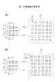
図1(A)及び(B)は、第1の実施例による半導体装置のビアホール部分の断面図を示す。図1(C)は、開口検査用パターンの概略平面図を示す。図1(C)の一点鎖線A1−A1における断面図が図1(A)及び(B)に相当する。以下、図1(A)の状態に至るまでの工程を説明する。
【0028】
SiO2からなる層間絶縁膜1の上に、SiNからなる厚さ50nmのエッチングストッパ膜2を、プラズマ励起型化学気相成長(プラズマCVD)により成膜する。エッチングストッパ膜2の上に、SiO2からなる厚さ500nmの配線層絶縁膜3を、プラズマCVDにより成膜する。
【0029】
配線層絶縁膜3の表面上にレジスト膜を形成し、このレジスト膜に、配線溝4に対応する開口を形成する。レジスト膜をマスクとして、配線層絶縁膜3をCF系エッチングガスを用いてドライエッチングし、エッチングストッパ膜2でエッチングを停止させる。配線層絶縁膜3に配線溝4が形成される。レジスト膜を除去した後、配線溝4の底面に露出しているエッチングストッパ膜2を、CHF系エッチングガスを用いてドライエッチングする。
【0030】
配線溝4の内面及び配線層絶縁膜3の上面を被覆するように、Taからなる厚さ30nmのバリアメタル層5Aを、スパッタリングにより成膜する。バリアメタル層5Aの上面に、銅(Cu)からなる厚さ200nmのシード層を、スパッタリングにより成膜する。このシード層上に、Cuを厚さ1500nmになるまでメッキする。配線溝4の内部がCuからなる主配線材5Bで埋め込まれる。配線層絶縁膜3の上面が露出するまで化学機械研磨(CMP)を行う。配線溝4内に、バリアメタル層5Aと主配線材5Bとからなる開口検査用の配線5が残る。
【0031】
配線5は、図1(C)に示すように、例えば相互に平行に配置された3本の配線で構成されている。3本の配線は、同一配線層に形成されたパッド15に連続している。パッド15は、配線5の形成と同時に形成される。
【0032】
配線層絶縁膜3の上に、SiNからなる厚さ50nmのエッチングストッパ膜10を、プラズマCVDにより形成する。エッチングストッパ膜10の上に、SiO2からなる厚さ1200nmの層間絶縁膜11を、プラズマCVDにより形成する。CMPを行うことにより、層間絶縁膜11の表面を平坦化する。平坦化後の層間絶縁膜11の厚さを、例えば800nm程度とする。
【0033】
層間絶縁膜11の上にレジスト膜を形成し、このレジスト膜にビアホール12に対応する開口を形成する。レジスト膜をマスクとし、CF系ガスを用いて、層間絶縁膜11をドライエッチングし、エッチングストッパ膜10でエッチングを停止させる。層間絶縁膜11に、開口検査用のビアホール12が形成される。その後、レジスト膜を除去する。
【0034】
ビアホール12の底面に露出したエッチングストッパ膜10を、CHF系ガスを用いてドライエッチングし、ビアホール12の底面に、配線層絶縁膜3及び配線5の上面の一部を露出させる。ビアホール12は、図1(C)に示すように、3行3列の行列状に配置されている。ビアホール12の3つの行が、それぞれ3本の配線12に対応している。
【0035】
位置ずれが全くない理想的な状態では、基板表面の法線に平行な視線で見たとき、中央の行のビアホール12が、中央の配線5の内部に収まり、最上行及び最下行のビアホール12は、対応する配線5からややずれており、ビアホール12の内側を、対応する配線5の縁が通過する。このような配置にしておくと、配線5とビアホール12との位置ずれが生じた場合であっても、いずれかの行のビアホール12の内部を、対応する配線5の縁が通過する。
【0036】
ビアホール12の底面をSEMで観察したところ、配線5の縁を明瞭に検出することができた。これは、配線5が、面積の大きなパッド15に接続されているため、SEMによる観察時に配線5に照射される電子の多くがパッド15に流入し、配線5への電荷の蓄積を抑制できたためと考えられる。
【0037】
配線5への電荷の蓄積を抑制するためには、必ずしも配線5と同一配線層内のパッド15に接続する必要はなく、同一配線層内またはそれよりも下層の大きな導電性領域に接続すればよい。配線5への電荷の蓄積を十分抑制するために、この導電性領域は、少なくとも配線5よりも大きな領域を占める大きさとすることが好ましい。導電性領域として、パッド以外に、半導体基板自体、チップの周囲に配置される耐湿リング、半導体基板上のゲート電極と同時に形成される導電領域等が挙げられる。これらの実施例については、後に説明する。
【0038】
開口検査により、ビアホール12の底面に配線5が露出していることが確認されると、次工程に進む。次工程では、図1(B)に示すように、ビアホール12が導電プラグ16で埋め込まれる。導電プラグ16は、バリアメタル層16A及び主導電材16Bで構成される。導電プラグ16は、配線5の形成方法と同様の方法で形成される。
【0039】
上記第1の実施例では、ビアホール12の底面をSEMで観察する場合を例にとって説明したが、SEM以外に、一般的に試料からの二次電子や反射電子の強度分布を利用して画像情報を得る観測装置を用いる場合にも、同様の効果が得られるであろう。
【0040】
図2に第1の実施例の変形例による半導体装置の平面図を示す。なお、図2(A)及び(B)の一点鎖線A1−A1における断面図が、第1の実施例における図1(A)の断面図と同一になる。
【0041】
図2(A)に示すように、パッド15の内部に、複数のビアホール30が配置されている。ビアホール30は、図1(A)に示したビアホール12と同様に、層間絶縁膜11及びエッチングストッパ膜10を貫通し、パッド15の上面を露出させる。層間絶縁膜11の上に、上層のパッドが形成される。上層のパッドは、ビアホール30内に埋め込まれる導電プラグを介して、下層のパッド15に接続される。
【0042】
図2(B)に示す変形例では、パッド15の下のビア層絶縁膜にも、ビアホール31が形成されている。ビアホール31内に埋め込まれた導電プラグを介してパッド15が、さらに下層のパッドに接続される。
【0043】
このように、配線5を、当該配線層のパッド15のみならず下層のパッドにも接続することにより、配線5への電荷の蓄積をより低減することができる。
【0044】
図3に、第1の実施例の他の変形例を示す。図3(A)は、ビアホール部の平面図を示し、図3(B)は、図3(A)の一点鎖線B3−B3における断面図を示す。配線5にパッド15が接続されている。配線5の上に配置された層間絶縁膜11に、ビアホール12が形成され、さらにビアホール12を内包するように、層間絶縁膜11の深さ方向の途中まで達する配線溝13が形成されている。図3(A)に示した平面図において、ビアホール12の内部を、配線5の縁が通過している。
【0045】
図3(C)に、ビアホール12の底面のSEM写真を示す。配線5の縁が明瞭に検出されることがわかる。
【0046】
図4に、第2の実施例による半導体装置の開口検査パターンの平面図を示す。3本の配線5、パッド15、3行3列の行列状に配置されたビアホール12は、図1(A)に示した実施例の構成と同様である。第2の実施例では、3本の配線5の両側に、さらに配線5と平行に、複数のダミー配線5aが配置されている。ダミー配線5aは電気的に孤立しており、他の導電性領域に接続されていない。
【0047】
配線5とダミー配線5aとが、検査用配線領域20内に均等に分布している。このように、複数の配線が高密度に分布すると、配線5を形成するためのCMP後に、図1(A)に示した配線層絶縁膜3の上面のうち、検査用配線領域20の部分に、エロージョンと呼ばれる窪みが生ずる。配線層絶縁膜3の上の層間絶縁膜11は平坦化されているため、配線5の上方の層間絶縁膜11が、窪みの深さ分だけ厚くなる。
【0048】
第2の実施例では、エロージョンの発生により層間絶縁膜11の厚さが不均一になった場合にも、信頼性の高い開口検査を行うことができる。検査用配線領域20に、積極的にエロージョンを発生させるためには、検査用配線領域20内の配線部分の面積を、検査用配線領域20の面積の25%以上とすることが好ましい。例えば、配線5及びダミー配線5aの幅W1を0.2μmとし、配線の間隔S1を0.6μmとすればよい。
【0049】
エロージョンによる窪みをより深くしたい場合には、例えば、配線幅W1と間隔S1を共に1μmにして、検査用配線領域20内の配線部分の面積を、検査用配線領域20の面積の50%程度にすればよい。検査用配線領域20内の配線の面積割合を、チップ内の最も開口しにくい場所、すなわちエロージョンによって最も深い窪みが生ずる場所の配線の面積割合と同程度にしておくことにより、検査用配線領域20内の開口検査により、チップ全体の開口の状態を判断することができる。
【0050】
図5(A)及び(B)に、それぞれ第3の実施例による半導体装置の断面図及び平面図を示す。図5(A)は、図5(B)の一点鎖線A5−A5における断面図に相当する。
【0051】
第1の実施例では、図1(C)に示したように、配線5が、パッド15に接続されていたが、第3の実施例では、配線5が、耐湿リング16に接続されている。耐湿リング16は、配線5の形成工程と同一の工程で形成され、チップの外周に沿って一周している。配線5とビアホール12との配置は、図1(A)及び(B)に示した第1の実施例による半導体装置のものと同様である。
【0052】
層間絶縁膜11及びエッチングストッパ膜10に、耐湿リング用溝17が形成されている。耐湿リング用溝17は、ビアホール12の形成工程と同一の工程で形成され、下層の耐湿リング16の上に配置される。
【0053】
第3の実施例では、耐湿リング16が、第1の実施例におけるパッド15と同様に、配線5への電荷の蓄積を抑制する。このため、容易に開口検査を行うことができる。
【0054】
図6(A)及び(B)に、それぞれ第4の実施例による半導体装置の断面図及び平面図を示す。図6(A)は、図6(B)の一点鎖線A6−A6における断面図に相当する。
【0055】
図6(A)に示すように、シリコンからなる半導体基板25の表面上に、シリコン局所酸化(LOCOS)またはシャロートレンチアイソレーション(STI)による素子分離絶縁領域26が形成されている。基板25の表面を、SiNからなるエッチングストッパ膜27が覆う。エッチングストッパ膜27の上に、SiO2からなる層間絶縁膜1が形成されている。層間絶縁膜1よりも上の層は、図5(A)に示した第3の実施例による半導体装置の構成と同一である。
【0056】
層間絶縁膜1及びエッチングストッパ膜27に形成された溝内に、耐湿リング28が埋め込まれている。耐湿リング28は、溝の内面を覆うTiNからなるバリアメタル層28Aと、溝内を埋め込むタングステンからなる主導電材28Bにより構成される。耐湿リング28は、配線5を基板25に電気的に接続している。配線5が基板25に接続されているため、配線5への電荷の蓄積を防止することができる。なお、配線5は、耐湿リング28を経由して基板に接続する代わりに、通常の導電プラグを経由して基板に接続してもよい。
【0057】
図7に第5の実施例による半導体装置の断面図を示す。半導体基板25の表面上に素子分離絶縁領域35が形成され、活性領域が画定されている。活性領域は、p型またはn型ウェル内に配置される。
【0058】
活性領域の一部の上に、SiO2膜36、ポリシリコン膜37、TiSiまたはCoSi等のシリサイド膜38の3層からなる積層構造が形成されている。この積層構造の側面上に、SiO2からなるサイドウォールスペーサ39が形成されている。SiO2膜36及びポリシリコン膜37は、それぞれ半導体基板の他の領域上に配置されるMOSFETのゲート絶縁膜及びゲート電極の形成と同時に形成される。シリサイド膜38は、周知のサリサイド(自己整合シリサイド)プロセスにより形成される。
【0059】
この積層構造の両側の、半導体基板25の表層部に、不純物注入領域41が形成されている。不純物注入領域41は、MOSFETのソース領域及びドレイン領域を形成するためのイオン注入と同一の工程で形成される。不純物注入領域41の上面が、TiSiまたはCoSi等のシリサイド膜42で覆われている。シリサイド膜42は、シリサイド膜38と同時に形成される。
【0060】
積層構造を覆うように、半導体基板25の上に、SiNからなるエッチングストッパ膜27が形成され、その上に、SiO2からなる層間絶縁膜1が形成されている。層間絶縁膜1よりも上層の構造は、図5(A)に示した第3の実施例による半導体装置の構造と同様である。
【0061】
層間絶縁膜1に、シリサイド膜38の一部を露出させるビアホールが形成され、このビアホール内に導電プラグ40が埋め込まれている。導電プラグ40は、ビアホールの内面を覆うTiNからなるバリアメタル層40Aと、ビアホール内を埋め込むタングステンからなる主導電材40Bにより構成される。導電プラグ40は、配線5をシリサイド膜38に接続する。これにより、配線5がポリシリコン膜37に電気的に接続される。ポリシリコン膜37と半導体基板25とは、SiO2膜36を挟んでキャパシタを構成する。
【0062】
図6(A)に示した第4の実施例では、配線5が、直接、半導体基板25に電気的に接続されていた。第5の実施例では、ポリシリコン膜37と半導体基板25とで構成されるキャパシタを介して、配線5が半導体基板25に接続される。
【0063】
ビアホール12の底面をSEMで観察するときに、配線5に入射した電子の多くは、ポリシリコン膜37と半導体基板25とで構成されるキャパシタに蓄積される。このため、配線5に蓄積される電荷量を少なくすることができる。
【0064】
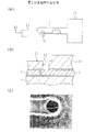
上記第1〜第5の実施例では、基板法線に平行な視線で見たとき、配線の縁がビアホール内部を通過するように、配線とビアホールとを配置したが、配線が太くなると、この方法で信頼性の高い開口検査を行うことが困難になる。以下、この課題について説明する。
【0065】
図8に示すように、配線層絶縁膜50に、細い配線51a及び太い配線51bが埋め込まれている。配線を形成するためのCMPにより、太い配線51bの上面に窪みが形成されている。配線51a、51b、及び配線層絶縁膜50の上に、エッチングストッパ膜52及びビア層絶縁膜53が、この順番に積層されている。
【0066】
ビア層絶縁膜53の表面は、CMPにより平坦化されている。このため、ビア層絶縁膜53は、太い配線51bの中央部上において厚くなる。太い配線51bの縁に重なるようにビアホール54aを形成して開口検査を行い、配線51bが露出していることが確認されたとしても、配線51bの中央部に配置されたビアホール54bが、配線51bの上面まで達している保証はない。チップ内には、太い配線の中央部にビアホールが配置される構造もあり得る。このため、太い配線51bの縁に重なるビアホール54aのみを用いた開口検査では、高い信頼性を確保することができない。以下に説明する第6の実施例では、太い配線の中央にビアホールが配置される場合にも、信頼度の高い開口検査を行うことができる。
【0067】
図9(A)に、第6の実施例による半導体装置の断面図を示し、図9(B)にその平面図を示す。図9(B)の一点鎖線A9−A9における断面図が、図9(A)に相当する。図9(A)に示した断面構造は、図1(A)に示した第1の実施例に示した半導体装置の断面構造とほぼ同様である。第1の実施例では、配線が、その上面に窪みが形成されない程度の太さであったが、第6の実施例の場合には、配線5が太いため、その上面に窪みが形成されている。
【0068】
太い配線5の内部に、配線層絶縁膜3の一部が残された絶縁領域3aが配置されている。すなわち、配線5が、絶縁領域3aを取り囲んでいる。図9(B)では、3個の絶縁領域3aが、配線5の長さ方向に並んで配置されている。なお、配線5の幅方向に関して、絶縁領域3aの位置が相互にずれている。絶縁領域3aは、配線5の上面の窪みが最も深くなる位置に配置することが好ましい。
【0069】
絶縁領域3aの各々に対応してビアホール12が配置されている。3つのビアホール12は、配線5の幅方向に関して同一の位置に配置されている。基板表面の法線に平行な視線で見たとき、ビアホール3aの少なくとも1つが、対応する絶縁領域3aの縁に重なるように配置されている。太い配線5は、図1に示した第1の実施例の場合と同様に、パッド15に接続されている。
【0070】
ビアホール12が配線5まで達すると、その底面に、配線5と絶縁領域3aとの境界線が現れる。この境界線をSEM等で観察することにより、開口検査を行うことができる。開口検査を行うためのビアホール12が、配線5の上の層間絶縁膜11の厚い部分を貫通する。このため、信頼性の高い開口検査を行うことができる。
【0071】
絶縁領域3aと、それに対応するビアホール12との3つの組について、配線5の幅方向に関する両者の相対的な位置関係が異なる。このため、位置合わせに若干のずれが生じたとしても、3つの組のいずれかにより、開口検査を行うことができる。
【0072】
次に、図10〜図12を参照して、上記実施例による半導体装置を開口検査用パターンとして含む半導体装置の製造方法を説明する。
【0073】
図10(A)に示すように、下地層111の上に、エッチングストッパ膜112を形成し、その上に配線層絶縁膜113を形成する。下地層111は、例えば半導体ウエハの活性領域にMOSFETを形成した後、その表面上に絶縁膜を形成し、この絶縁膜に導電プラグを埋め込んだ構造、またはそれよりも上層のビア層絶縁膜に導電プラグを埋め込んだ構造を有する。
【0074】
エッチングストッパ膜112は、例えば厚さ50nmのSiN膜で構成され、SiN膜は、エッチングストッパ機能及びCu拡散防止機能を有する。配線層絶縁膜113は、例えばSiO2からなる厚さ500nmの膜である。配線層絶縁膜113の表面上に、配線パターンに対応する開口を有するレジスト膜114を形成する。
【0075】
レジスト膜114をエッチングマスクとし、CF系エッチングガスを用いた反応性イオンエッチング(RIE)により、配線層絶縁膜113をエッチングし、エッチングストッパ膜112でエッチングを停止させる。その後、酸素プラズマを用いたアッシングにより、レジスト膜114を除去する。このアッシング時に、下地層111がエッチングストッパ膜112で覆われているため、その下に配置された導電体表面の酸化が防止される。その後、配線層絶縁膜113に形成された溝の底面に露出したエッチングストッパ膜112を、CHF系エッチングガスを用いたRIEにより除去する。ここまでの工程で、配線用の溝が形成される。
【0076】
この配線層絶縁膜113及びエッチングストッパ膜112に、上記第1〜第6の実施例で説明した開口検査用のビアホールを形成することにより、開口検査が行われる。
【0077】
図10(B)に示すように、配線溝を形成した構造の上に、バリアメタル層115及び主配線層116を形成する。バリアメタル層115は、例えばTaからなる厚さ50nmの膜であり、スパッタリングにより形成される。主配線層116は、Cuからなる膜であり、スパッタリングやメッキにより形成される。メッキにより形成する場合は、まずCuシード層をスパッタリングで形成し、その上にCuをメッキすることにより形成する。
【0078】
バリアメタル層115及び主配線層116を形成した後、CMPを行い、配線層絶縁膜113の上面よりも上の主配線層116及びバリアメタル層115を除去する。
【0079】
図10(C)に示すように、配線層絶縁膜113に形成された配線溝内に、バリアメタル層115及び主配線層116からなる配線が残る。この時、開口検査用の配線5も形成される。開口検査用の配線5は、チップ内に配置してもよいし、スクライブライン上に配置してもよい。配線層絶縁膜113の上に、第2層目のエッチングストッパ膜117を形成する。エッチングストッパ膜117は、例えばSiNからなる厚さ50nmの膜である。エッチングストッパ膜117の上に、ビア層絶縁膜118を形成する。ビア層絶縁膜118は、例えばSiO2からなる厚さ1200nmの膜である。
【0080】
ビア層絶縁膜118を形成した後、CMPを行い、その表面を平坦化する。平坦化後のビア層絶縁膜118の上に、第3層目のエッチングストッパ膜119及び配線層絶縁膜120を形成する。エッチングストッパ膜119は、例えばSiNからなる厚さ50nmの膜である。配線層絶縁膜120は、例えばSiO2からなる厚さ500nmの膜である。配線層絶縁膜120の上に、ビアホール形成用の開口を有するレジスト膜121を形成する。
【0081】
レジスト膜121をエッチングマスクとし、CF系エッチングガス、CHF系エッチングガス等を用い、配線層絶縁膜120、エッチングストッパ膜119、ビア層絶縁膜118をエッチングする。エッチング条件を制御することにより、エッチングストッパ膜117の表面でエッチングを停止させる。酸素プラズマを用いたアッシングにより、レジスト膜121を除去する。これにより、エッチングストッパ膜117まで達するビアホールが形成される。この時、開口検査用のビアホール12も形成される。
【0082】
図11(D)に示すように、配線層絶縁膜120の表面上に非感光性樹脂を塗布し、表面から溶融させることにより、ビアホール内にのみ非感光性樹脂の詰物122を残す。その後、配線層絶縁膜120の表面上に、配線に対応する開口を有するレジスト膜123を形成する。
【0083】
レジスト膜123をエッチングマスクとし、CF系ガスを用いたRIEにより、配線層絶縁膜120をエッチングする。このエッチングは、エッチングストッパ膜119の表面で停止する。これにより、配線層絶縁膜120に配線溝が形成される。
【0084】
図11(E)に示すように、酸素プラズマを用いたアッシングにより、レジスト膜122を除去する。このとき、非感光性樹脂の詰物122も除去される。配線溝及びビアホールの底面に、それぞれエッチングストッパ膜119及び117が露出する。
【0085】
図11(F)に示すように、露出したエッチングストッパ膜119及び117を、CHF系エッチングガスを用いたRIEにより除去する。この状態で開口検査用のビアホール12の底面を観察することにより、開口検査を行うことができる。
【0086】
図12(G)に示すように、配線層絶縁膜120の上面、配線溝及びビアホールの内面を覆うバリアメタル層124を形成し、その上に主配線層125を形成する。バリアメタル層124及び主配線層125は、下層のバリアメタル層115及び主配線層116と同様の方法で形成される。配線層絶縁膜120の上面よりも上方に堆積したバリアメタル層124及び主配線層125をCMPにより除去する。
【0087】
図12(H)に示すように、CMP後の平坦化された表面を、第4層目のエッチングストッパ膜126で覆う。このようにして、デュアルダマシン構造の配線125が形成される。
【0088】
図10〜図12では、実施例による半導体装置の開口検査パターンを、デュアルダマシン構造に適用した場合の製造方法を説明したが、シングルダマシン構造に適用することも可能である。
【0089】
図13に、ダマシン構造による多層配線を有する半導体装置の断面図の一例を示す。ウエルを形成した半導体ウエハ201の所定領域に、素子分離用溝が形成され、酸化シリコン等の絶縁物が埋め込まれ、シャロートレンチアイソレーション(STI)による素子分離絶縁領域204が形成されている。
【0090】
素子分離絶縁領域204で画定された活性領域上に、絶縁ゲート電極205、サイドウォールスペーサ206が形成され、その両側にソース/ドレイン領域S/Dがイオン注入により形成される。絶縁ゲート電極205を覆うように、第1エッチングストッパ膜210が形成され、その上に第1下部絶縁膜211が形成される。第1下部絶縁膜211、第1エッチングストッパ膜210を貫通して、導電プラグがバリアメタル層207、配線金属領域208により形成される。
【0091】
第1下部絶縁膜211の上に、有機絶縁膜212、第1上部絶縁膜213が形成される。有機絶縁膜が塗布型であれば平坦化機能を有するため、CMPを行わなくても平坦な表面が得られる。第1上部絶縁膜213、有機絶縁膜212に配線溝を形成し、第1配線209を埋め込む。
【0092】
第1配線209の表面上に第2エッチングストッパ膜220、第2下部絶縁膜221が形成され、CMPにより平坦化される。第2下部絶縁膜221の上に、第2有機絶縁膜222、第2上部絶縁膜223が形成され、デュアルダマシン配線構造224が形成される。
【0093】
同様に、第2上部絶縁膜223の表面上に第3エッチングストッパ膜230、第3下部絶縁膜231が形成され、CMPにより平坦化される。その上に第3有機絶縁膜232、第3上部絶縁膜233が形成され、第2デュアルダマシン配線構造234が形成される。
【0094】
さらに、第3上部絶縁膜233の上に、第4エッチングストッパ膜240、第4下部絶縁膜241が形成され、CMPにより平坦化される。第4下部絶縁膜241の上に、第4有機絶縁膜242、第4上部絶縁膜243が形成され、第3デュアルダマシン配線構造244が形成される。これらの配線の表面に、表面保護膜250が形成される。
【0095】
これら多層配線の各層にビアホールを形成する工程で、上記実施例による開口検査が行われる。
【0096】
なお、4層の多層配線構造を形成する場合を説明したが、配線層の数は任意に増減することができる。又、有機絶縁膜と上部絶縁膜との積層の代わりに、エッチングストッパ膜と絶縁膜との積層を用いてもよい。弗素や炭素を含む酸化シリコン膜や多孔質酸化シリコン膜等の低誘電率絶縁膜を含む積層構造を用いることもできる。
【0097】
以上実施例に沿って本発明を説明したが、本発明はこれらに制限されるものではない。例えば、種々の変更、改良、組み合わせ等が可能なことは当業者に自明であろう。
【0098】
上記実施例から、以下の付記に示された発明が導き出される。
(付記1) (a)第1の表面を画定する基板の、絶縁材料からなる表層部に設けられた配線溝に導電材料からなる配線が埋め込まれ、該配線の上面が該第1の表面に露出し、該配線が導電性部材に電気的に接続されており、該第1の表面の法線に平行な視線で見たとき、該導電性部材が該配線よりも大きな領域を占めている基板の該第1の表面上に、絶縁材料からなる第1の膜を形成する工程と、
(b)前記第1の膜にビアホールを形成する工程であって、前記第1の表面の法線に平行な視線で見たとき、前記配線と、絶縁材料からなる前記表層部との境界が該ビアホール内を通過するように前記ビアホールを形成する工程と、
(c)前記ビアホールの底面を、試料からの二次電子や反射電子の強度分布を利用して画像情報を得る装置で観察し、該ビアホールの底面の状態の良否を判定する工程と
有する半導体装置の製造方法。
(付記2) 前記導電性部材が、前記配線と同一配線層またはそれよりも下の配線層に配置されているパッドまたは耐湿リングである付記1に記載の半導体装置の製造方法。
(付記3) 前記基板が、半導体基板と、該半導体基板の表面上に形成された多層配線とを含み、前記導電性部材が前記半導体基板である付記1に記載の半導体装置の製造方法。
(付記4) 前記基板が、半導体基板と、該半導体基板の表面上に形成され、ソース領域、ドレイン領域、ゲート絶縁膜、ゲート電極を含むMOS型トランジスタと、前記半導体基板の表面上に形成され、前記ゲート絶縁膜と同一材料かつ同一膜厚のキャパシタ誘電体膜とを有し、
前記導電性部材が、前記キャパシタ誘電体膜の上に形成され、前記半導体基板を一方の電極とするキャパシタを構成している付記1に記載の半導体装置の製造方法。
(付記5) 前記工程(a)が、
前記第1の表面よりも深い位置にある第2の表面上に配置され、絶縁材料からなる第2の膜であって、該第2の膜の上面が前記第1の表面を画定する該第2の膜を形成する工程と、
前記第2の膜に、前記配線溝を形成する工程と、
前記配線溝の内部を埋め込むように、前記第2の膜の上に導電膜を堆積する工程と、
前記導電膜のうち、前記第1の表面よりも上方に堆積している部分を除去し、前記配線溝内に前記配線を残す工程と
を含む付記1乃至4のいずれかに記載の半導体装置の製造方法。
(付記6) 前記第1の膜が、
前記第1の表面上に直接配置され、前記第1の表面を画定する表層部とは異なる材料で形成されたエッチングストッパ膜と、
前記エッチングストッパ膜の上に配置され、該エッチングストッパ膜とは異なる材料で形成された層間絶縁膜と
を含み、
前記工程(b)が、
前記エッチングストッパ膜のエッチング速度が、前記層間絶縁膜のエッチング速度よりも遅くなる条件で、該層間絶縁膜に前記ビアホールを形成する工程と、前記第1の表面を画定する表層部のエッチング速度が、前記エッチングストッパ膜のエッチング速度よりも遅くなる条件で、前記ビアホールの底面のエッチングストッパ膜を除去する工程と
を含む付記1乃至5のいずれかに記載された半導体装置の製造方法。
(付記7) 前記配線の両側に、該配線に平行に、複数の他の配線が配置されている付記1乃至6のいずれかに記載の半導体装置の製造方法。
(付記8) 前記複数の配線が、前記第1の表面の第1の領域内に均等に配置されており、該第1の領域内の配線部分の面積が、該第1の領域の面積の25%以上である付記7に記載の半導体装置の製造方法。
(付記9) 前記第1の表面内において、前記第1の領域が、その周囲の領域よりも窪んでいる付記8に記載の半導体装置の製造方法。
(付記10) 前記第1の表面内において、前記配線が絶縁領域を取り囲んでおり、前記第1の表面の法線に平行な視線で見たとき、前記ビアホール内を、該配線と該絶縁領域との境界線が通過するように、該ビアホールを配置する付記1乃至6のいずれかに記載の半導体装置の製造方法。
(付記11) 前記第1の表面内において、前記配線の上面が窪んでおり、前記絶縁領域の上面が、前記配線の周囲よりも低くなっている付記10に記載の半導体装置の製造方法。
(付記12) 第1の表面を画定する基板の、絶縁材料からなる表層部に設けられた配線溝に導電材料からなる配線が埋め込まれ、該配線の上面が該第1の表面に露出し、該配線が第1の導電性部材に電気的に接続されており、該第1の表面の法線に平行な視線で見たとき、該第1の導電性部材が該配線よりも大きな領域を占めている基板と、
前記基板の前記第1の表面上に形成された絶縁材料からなる第1の膜と、
前記第1の膜に形成されたビアホールであって、該第1の表面の法線に平行な視線で見たとき、前記配線と、絶縁材料からなる前記表層部との境界が該ビアホール内を通過するように配置されている前記ビアホールと、
前記ビアホール内に埋め込まれ、底面において前記配線に接続された第2の導電性部材と
を有し、該第2の導電性部材の底面が、前記配線の縁に対応する位置に段差を有しない半導体装置。
(付記13) 前記第1の導電性部材が、前記配線と同一配線層またはそれよりも下の配線層に配置されているパッドまたは耐湿リングである付記12に記載の半導体装置。
(付記14) 前記基板が、半導体基板と、該半導体基板の表面上に形成された多層配線とを含み、前記第1の導電性部材が前記半導体基板である付記12に記載の半導体装置。
(付記15) 前記基板が、半導体基板と、該半導体基板の表面上に形成され、ソース領域、ドレイン領域、ゲート絶縁膜、ゲート電極を含むMOS型トランジスタと、前記半導体基板の表面上に形成され、前記ゲート絶縁膜と同一材料かつ同一膜厚のキャパシタ誘電体膜とを有し、
前記第1の導電性部材が、前記キャパシタ誘電体膜の上に形成され、前記半導体基板を一方の電極とするキャパシタを構成している付記12に記載の半導体装置。
(付記16) 前記第1の膜が、
前記第1の表面上に直接配置され、前記第1の表面を画定する表層部とは異なる材料で形成されたエッチングストッパ膜と、
前記エッチングストッパ膜の上に配置され、該エッチングストッパ膜とは異なる材料で形成された層間絶縁膜と
を含む付記12乃至15のいずれかに記載された半導体装置。
(付記17) 前記配線の両側に、該配線に平行に、複数の他の配線が配置されている付記12乃至16のいずれかに記載の半導体装置。
(付記18) 前記複数の配線が、前記第1の表面の第1の領域内に均等に配置されており、該第1の領域内の配線部分の面積が、該第1の領域の面積の25%以上である付記17に記載の半導体装置。
(付記19) 前記第1の表面内において、前記第1の領域が、その周囲の領域よりも窪んでいる付記18に記載の半導体装置。
(付記20) 前記第1の表面内において、前記配線が絶縁領域を取り囲んでおり、該第1の表面の法線に平行な視線で見たとき、前記ビアホール内を、該配線と該絶縁領域との境界線が通過するように、該ビアホールが配置されている付記12乃至16のいずれかに記載の半導体装置。
(付記21) 前記第1の表面内において、前記配線の上面が窪んでおり、前記絶縁領域の上面が、前記配線の周囲よりも低くなっている付記20に記載の半導体装置。
【0099】
【発明の効果】
以上説明したように、本発明によれば、開口検査用の配線が、大きな導電性部材に接続されているため、配線への電荷の蓄積が低減され、二次電子や反射電子の強度分布を利用して明瞭な画像を得ることができる。配線と、絶縁材料からなる表層部との境界がビアホール内を通過するため、ビアホールの底面を観察して境界線の有無を検出することにより、配線が露出したか否かを判定することができる。
【図面の簡単な説明】
【図1】 第1の実施例による半導体装置の断面図及び平面図である。
【図2】 第1の実施例の変形例による半導体装置の平面図である。
【図3】 第1の実施例の他の変形例による半導体装置の平面図、断面図、及びSEM写真である。
【図4】 第2の実施例による半導体装置の平面図である。
【図5】 第3の実施例による半導体装置の断面図及び平面図である。
【図6】 第4の実施例による半導体装置の断面図及び平面図である。
【図7】 第5の実施例による半導体装置の断面図である。
【図8】 太い配線が配置された領域における開口検査の問題点を説明するための開口検査用ビアホール部の断面図である。
【図9】 第6の実施例による半導体装置の断面図及び平面図である。
【図10】 上記実施例による半導体装置に用いられる開口検査用構造を適用することが可能な半導体装置の製造方法を説明するための断面図(その1)である。
【図11】 上記実施例による半導体装置に用いられる開口検査用構造を適用することが可能な半導体装置の製造方法を説明するための断面図(その2)である。
【図12】 上記実施例による半導体装置に用いられる開口検査用構造を適用することが可能な半導体装置の製造方法を説明するための断面図(その3)である。
【図13】 上記実施例による半導体装置に用いられる開口検査構造を適用することが可能な半導体装置の断面図である。
【図14】 従来の開口検査及び位置ずれ検査を行うためのビアホール及び配線の断面図である。
【図15】 従来の開口検査を行うためのビアホール及び配線の断面図である。
【図16】 従来の開口検査を行うためのビアホール及び配線の断面図である。
【図17】 従来の開口検査方法を、ダマシン構造の配線に適用した場合のビアホール部の断面図及びSEM写真である。
【符号の説明】
1、11、53、211 層間絶縁膜
2、10、27、52、112、115、117、119、126、210、220、230、240 エッチングストッパ膜
3、50、113、120 配線層絶縁膜
3a 絶縁領域
4 配線溝
5、51a、51b 配線
12、30、31、54a、54b ビアホール
15 パッド
16 耐湿リング
17 耐湿リング用溝
20 検査用配線領域
25、201 半導体基板
26、35、204 素子分離絶縁領域
28 耐湿リング
36 SiO2膜
37 ポリシリコン膜
38 シリサイド膜
39、206 サイドウォールスペーサ
40 導電プラグ
41 不純物注入領域
111 下地層
114、121、123 レジスト膜
116、125、208 主配線層
118 ビア層絶縁膜
122 詰物
124、207 バリアメタル層
205 ゲート電極
209、224、234、244 デュアルダマシン構造配線
212、222、232、242 有機絶縁膜
213、223、233、243 上部絶縁膜
221、231、241 下部絶縁膜
250 表面保護膜[0001]
BACKGROUND OF THE INVENTION
The present invention relates to a method for manufacturing a semiconductor device and a semiconductor device, and more particularly to a method for manufacturing a semiconductor device for inspecting opening of a via hole formed in an insulating film on a wiring, and a semiconductor device manufactured by the manufacturing method.
[0002]
[Prior art]
When forming a via hole in an interlayer insulating film, several opening inspection methods for inspecting whether or not the via hole has reached the underlying surface of the interlayer insulating film are known.
[0003]
FIG. 14A shows a cross-sectional view of a via hole portion inspected by the opening inspection method disclosed in Japanese Patent Laid-Open No. 60-109240. A
[0004]
When the bottom surface of the
[0005]
Therefore, the opening inspection of the
[0006]
As shown in FIG. 14B, the
[0007]
FIG. 15 shows a cross-sectional view of a via hole portion inspected by the opening inspection method disclosed in Japanese Patent Laid-Open No. 4-12531.
[0008]
As shown in FIG. 15A, a
[0009]
As shown in FIG. 15B, when two
[0010]
FIG. 16 shows a cross-sectional view of a via hole portion inspected by the opening inspection method disclosed in Japanese Patent Application Laid-Open No. 11-297777. An
[0011]
An upper
[0012]
Even when the
[0013]
[Problems to be solved by the invention]
Compared to the conventional method of forming a wiring by patterning a metal layer by reactive ion etching (RIE), a damascene method that can easily meet the high density requirement of a semiconductor integrated circuit device and can be expected to reduce the number of processes has been attracting attention. The damascene method is suitable for forming copper wiring for reducing wiring resistance.
[0014]
FIG. 17A is a cross-sectional view of the via hole portion in the middle of the process of forming the copper wiring by the damascene method. A
[0015]
On the interlayer
[0016]
FIG. 17B shows an SEM photograph in the vicinity of the
[0017]
FIG. 17C is a cross-sectional view in which the via
[0018]
Under the etching conditions of the
[0019]
FIG. 17D shows an SEM photograph near the via
[0020]
In the conventional example shown in FIG. 16, the opening inspection is performed without using a step, but when the diameter of the via
[0021]
An object of the present invention is to provide a semiconductor device manufacturing method capable of performing a highly reliable opening inspection even when there is no step on the bottom surface of the via hole and the via hole diameter is reduced.
[0022]
Another object of the present invention is to provide a semiconductor device manufactured by the method for manufacturing a semiconductor device.
[0023]
[Means for Solving the Problems]
According to one aspect of the present invention, (a) a wiring made of a conductive material is embedded in a wiring groove provided in a surface layer portion made of an insulating material of a substrate that defines a first surface, and an upper surface of the wiring is An area where the conductive member is larger than the wiring when exposed to a line of sight parallel to the normal of the first surface. Forming a first film made of an insulating material on the first surface of the substrate occupying the substrate, and (b) forming a via hole in the first film, Forming the via hole so that a boundary between the wiring and the surface layer portion made of an insulating material passes through the via hole when viewed in a line of sight parallel to a normal line of the surface; (c) the via hole Image information on the bottom surface using the intensity distribution of secondary and reflected electrons from the sample Observed with that device, and determining the acceptability of the state of the bottom surface of the via hole The A method for manufacturing a semiconductor device is provided.
[0024]
According to another aspect of the present invention, a wiring made of a conductive material is embedded in a wiring groove provided in a surface layer portion made of an insulating material of a substrate that defines a first surface, and an upper surface of the wiring is The first conductive member is exposed to the surface, and the wiring is electrically connected to the first conductive member. When viewed in a line of sight parallel to the normal of the first surface, the first conductive member is A substrate occupying a larger area, a first film made of an insulating material formed on the first surface of the substrate, and a via hole formed in the first film, The via hole disposed so that a boundary between the wiring and the surface layer portion made of an insulating material passes through the via hole when viewed in a line of sight parallel to a normal line of the surface of the first surface; A second conductive member embedded and connected to the wiring on the bottom surface. , The bottom surface of the second conductive member, no stepped semiconductor device is provided in a position corresponding to the edge of the wiring.
[0025]
Since the wiring is connected to a large conductive member, charge accumulation in the wiring is reduced, and a clear image can be obtained using the intensity distribution of secondary electrons and reflected electrons. Since the boundary between the wiring and the surface layer portion passes through the via hole, it can be determined whether or not the wiring is exposed by observing the bottom surface of the via hole and detecting the presence or absence of the boundary line.
[0026]
DETAILED DESCRIPTION OF THE INVENTION
With reference to FIG. 1, a semiconductor device and a manufacturing method thereof according to a first embodiment of the present invention will be described.
[0027]
1A and 1B are cross-sectional views of the via hole portion of the semiconductor device according to the first embodiment. FIG. 1C is a schematic plan view of an opening inspection pattern. A cross-sectional view taken along one-dot chain line A1-A1 in FIG. 1C corresponds to FIGS. Hereinafter, steps required until the state shown in FIG.
[0028]
SiO 2 An
[0029]
A resist film is formed on the surface of the wiring
[0030]
A
[0031]
As shown in FIG. 1C, the
[0032]
An
[0033]
A resist film is formed on the
[0034]
The
[0035]
In an ideal state where there is no positional deviation, the via
[0036]
When the bottom surface of the via
[0037]
In order to suppress the accumulation of electric charges in the
[0038]
When the opening inspection confirms that the
[0039]
In the first embodiment, the case where the bottom surface of the via
[0040]
FIG. 2 is a plan view of a semiconductor device according to a modification of the first embodiment. 2A and 2B is the same as the cross-sectional view of FIG. 1A in the first embodiment.
[0041]
As shown in FIG. 2A, a plurality of via
[0042]
In the modification shown in FIG. 2B, the via
[0043]
In this way, by connecting the
[0044]
FIG. 3 shows another modification of the first embodiment. 3A is a plan view of the via hole portion, and FIG. 3B is a cross-sectional view taken along one-dot chain line B3-B3 in FIG. A
[0045]
FIG. 3C shows an SEM photograph of the bottom surface of the via
[0046]
FIG. 4 is a plan view of an opening inspection pattern of the semiconductor device according to the second embodiment. The via holes 12 arranged in a matrix of three
[0047]
The
[0048]
In the second embodiment, a highly reliable opening inspection can be performed even when the thickness of the
[0049]
In order to deepen the erosion depression, for example, both the wiring width W1 and the interval S1 are set to 1 μm, and the area of the wiring portion in the
[0050]
5A and 5B are a sectional view and a plan view of a semiconductor device according to the third embodiment, respectively. FIG. 5A corresponds to a cross-sectional view taken along dashed-dotted line A5-A5 in FIG.
[0051]
In the first embodiment, the
[0052]
A moisture-
[0053]
In the third embodiment, the moisture-
[0054]
6A and 6B are a sectional view and a plan view of a semiconductor device according to the fourth embodiment, respectively. FIG. 6A corresponds to a cross-sectional view taken along dashed-dotted line A6-A6 in FIG.
[0055]
As shown in FIG. 6A, an element
[0056]
A moisture-
[0057]
FIG. 7 is a sectional view of a semiconductor device according to the fifth embodiment. An element
[0058]
On part of the active region, SiO 2 A laminated structure including three layers of a
[0059]
Impurity implanted
[0060]
An
[0061]
A via hole that exposes a portion of the
[0062]
In the fourth embodiment shown in FIG. 6A, the
[0063]
When the bottom surface of the via
[0064]
In the first to fifth embodiments, the wiring and the via hole are arranged so that the edge of the wiring passes through the inside of the via hole when viewed with a line of sight parallel to the substrate normal line. This makes it difficult to perform highly reliable opening inspection. Hereinafter, this problem will be described.
[0065]
As shown in FIG. 8, a thin wiring 51 a and a
[0066]
The surface of the via
[0067]
FIG. 9A shows a cross-sectional view of the semiconductor device according to the sixth embodiment, and FIG. 9B shows a plan view thereof. A cross-sectional view taken along one-dot chain line A9-A9 in FIG. 9B corresponds to FIG. The cross-sectional structure shown in FIG. 9A is substantially the same as the cross-sectional structure of the semiconductor device shown in the first embodiment shown in FIG. In the first embodiment, the wiring has such a thickness that no depression is formed on the upper surface thereof. However, in the case of the sixth embodiment, since the
[0068]
An
[0069]
A via
[0070]
When the via
[0071]
Regarding the three sets of the
[0072]
Next, a method for manufacturing a semiconductor device including the semiconductor device according to the above embodiment as an opening inspection pattern will be described with reference to FIGS.
[0073]
As shown in FIG. 10A, an
[0074]
The
[0075]
Using the resist
[0076]
The opening inspection is performed by forming the via hole for opening inspection described in the first to sixth embodiments in the wiring
[0077]
As shown in FIG. 10B, a
[0078]
After forming the
[0079]
As shown in FIG. 10C, the wiring composed of the
[0080]
After the via
[0081]
Using the resist
[0082]
As shown in FIG. 11D, a non-photosensitive resin is applied on the surface of the wiring
[0083]
Using the resist
[0084]
As shown in FIG. 11E, the resist
[0085]
As shown in FIG. 11F, the exposed
[0086]
As shown in FIG. 12G, a
[0087]
As shown in FIG. 12H, the planarized surface after CMP is covered with a fourth-layer
[0088]
10 to 12, the manufacturing method in the case where the opening inspection pattern of the semiconductor device according to the embodiment is applied to the dual damascene structure has been described. However, the manufacturing method can also be applied to the single damascene structure.
[0089]
FIG. 13 shows an example of a cross-sectional view of a semiconductor device having a multilayer wiring with a damascene structure. An element isolation trench is formed in a predetermined region of the
[0090]
An
[0091]
An organic insulating
[0092]
A second
[0093]
Similarly, a third
[0094]
Further, a fourth
[0095]
In the step of forming a via hole in each layer of the multilayer wiring, the opening inspection according to the above embodiment is performed.
[0096]
Although the case where a four-layer multilayer wiring structure is formed has been described, the number of wiring layers can be arbitrarily increased or decreased. Further, instead of the stack of the organic insulating film and the upper insulating film, a stack of an etching stopper film and an insulating film may be used. A stacked structure including a low dielectric constant insulating film such as a silicon oxide film containing fluorine or carbon or a porous silicon oxide film can also be used.
[0097]
Although the present invention has been described with reference to the embodiments, the present invention is not limited thereto. It will be apparent to those skilled in the art that various modifications, improvements, combinations, and the like can be made.
[0098]
From the above examples, the invention shown in the following supplementary notes is derived.
(Appendix 1) (a) A wiring made of a conductive material is embedded in a wiring groove provided in a surface layer part made of an insulating material of a substrate that defines a first surface, and an upper surface of the wiring is formed on the first surface. Exposed, the wiring is electrically connected to the conductive member, and the conductive member occupies a larger area than the wiring when viewed in a line of sight parallel to the normal of the first surface Forming a first film made of an insulating material on the first surface of the substrate;
(B) a step of forming a via hole in the first film, and when viewed from a line of sight parallel to a normal line of the first surface, a boundary between the wiring and the surface layer portion made of an insulating material is Forming the via hole so as to pass through the via hole;
(C) observing the bottom surface of the via hole with an apparatus that obtains image information using the intensity distribution of secondary electrons and reflected electrons from the sample, and determining whether the state of the bottom surface of the via hole is good or bad;
A method for manufacturing a semiconductor device.
(Additional remark 2) The manufacturing method of the semiconductor device of
(Supplementary note 3) The method of manufacturing a semiconductor device according to
(Supplementary Note 4) The substrate is formed on a semiconductor substrate, a MOS transistor including a source region, a drain region, a gate insulating film, and a gate electrode formed on the surface of the semiconductor substrate, and on the surface of the semiconductor substrate. A capacitor dielectric film having the same material and the same film thickness as the gate insulating film,
The manufacturing method of the semiconductor device according to
(Additional remark 5) The said process (a),
A second film made of an insulating material and disposed on a second surface deeper than the first surface, the upper surface of the second film defining the first surface; Forming a second film;
Forming the wiring groove in the second film;
Depositing a conductive film on the second film so as to fill the inside of the wiring trench;
Removing the portion of the conductive film deposited above the first surface and leaving the wiring in the wiring trench;
A method for manufacturing a semiconductor device according to any one of
(Supplementary Note 6) The first film is
An etching stopper film that is disposed directly on the first surface and is formed of a material different from a surface layer portion that defines the first surface;
An interlayer insulating film disposed on the etching stopper film and formed of a material different from the etching stopper film;
Including
The step (b)
The step of forming the via hole in the interlayer insulating film under the condition that the etching rate of the etching stopper film is slower than the etching rate of the interlayer insulating film, and the etching rate of the surface layer portion defining the first surface is Removing the etching stopper film on the bottom surface of the via hole under a condition that is slower than the etching rate of the etching stopper film;
A method for manufacturing a semiconductor device according to any one of
(Additional remark 7) The manufacturing method of the semiconductor device in any one of
(Supplementary Note 8) The plurality of wirings are evenly arranged in the first region of the first surface, and the area of the wiring part in the first region is equal to the area of the first region. The method for manufacturing a semiconductor device according to appendix 7, wherein the manufacturing method is 25% or more.
(Supplementary note 9) The method for manufacturing a semiconductor device according to supplementary note 8, wherein the first region is recessed in a region around the first surface in the first surface.
(Supplementary Note 10) In the first surface, the wiring surrounds the insulating region, and when viewed in a line of sight parallel to the normal line of the first surface, the wiring and the insulating region are formed in the via hole. 7. The method of manufacturing a semiconductor device according to any one of
(Supplementary note 11) The method for manufacturing a semiconductor device according to
(Supplementary Note 12) A wiring made of a conductive material is embedded in a wiring groove provided in a surface layer portion made of an insulating material of a substrate that defines a first surface, and an upper surface of the wiring is exposed on the first surface, The wiring is electrically connected to the first conductive member. When viewed in a line of sight parallel to the normal of the first surface, the first conductive member has a larger area than the wiring. Occupying the substrate,
A first film made of an insulating material formed on the first surface of the substrate;
A via hole formed in the first film, and when viewed in a line of sight parallel to a normal line of the first surface, a boundary between the wiring and the surface layer portion made of an insulating material passes through the via hole. The via hole arranged to pass through;
A second conductive member embedded in the via hole and connected to the wiring on the bottom surface;
And the bottom surface of the second conductive member does not have a step at a position corresponding to the edge of the wiring.
(Supplementary note 13) The semiconductor device according to
(Supplementary note 14) The semiconductor device according to
(Supplementary Note 15) The substrate is formed on a semiconductor substrate, a MOS transistor including a source region, a drain region, a gate insulating film, and a gate electrode formed on the surface of the semiconductor substrate, and on the surface of the semiconductor substrate. A capacitor dielectric film having the same material and the same film thickness as the gate insulating film,
13. The semiconductor device according to
(Supplementary Note 16) The first film is
An etching stopper film that is disposed directly on the first surface and is formed of a material different from a surface layer portion that defines the first surface;
An interlayer insulating film disposed on the etching stopper film and formed of a material different from the etching stopper film;
A semiconductor device according to any one of
(Supplementary note 17) The semiconductor device according to any one of
(Supplementary Note 18) The plurality of wirings are evenly arranged in the first region of the first surface, and the area of the wiring part in the first region is equal to the area of the first region. Item 18. The semiconductor device according to
(Supplementary note 19) The semiconductor device according to supplementary note 18, wherein the first region is depressed more than a surrounding region in the first surface.
(Supplementary note 20) In the first surface, the wiring surrounds the insulating region, and when viewed in a line of sight parallel to the normal line of the first surface, the wiring and the insulating region are formed in the via hole. The semiconductor device according to any one of
(Supplementary note 21) The semiconductor device according to
[0099]
【The invention's effect】
As described above, according to the present invention, since the wiring for opening inspection is connected to a large conductive member, accumulation of electric charges in the wiring is reduced, and the intensity distribution of secondary electrons and reflected electrons is reduced. A clear image can be obtained by using it. Since the boundary between the wiring and the surface layer portion made of an insulating material passes through the via hole, it is possible to determine whether the wiring is exposed by observing the bottom surface of the via hole and detecting the presence or absence of the boundary line. .
[Brief description of the drawings]
FIG. 1 is a cross-sectional view and a plan view of a semiconductor device according to a first embodiment.
FIG. 2 is a plan view of a semiconductor device according to a modification of the first embodiment.
3 is a plan view, a cross-sectional view, and an SEM photograph of a semiconductor device according to another modification of the first embodiment. FIG.
FIG. 4 is a plan view of a semiconductor device according to a second embodiment.
FIG. 5 is a cross-sectional view and a plan view of a semiconductor device according to a third embodiment.
FIG. 6 is a cross-sectional view and a plan view of a semiconductor device according to a fourth embodiment.
FIG. 7 is a sectional view of a semiconductor device according to a fifth embodiment.
FIG. 8 is a cross-sectional view of an opening inspection via hole portion for explaining a problem of opening inspection in a region where a thick wiring is arranged.
FIG. 9 is a cross-sectional view and a plan view of a semiconductor device according to a sixth embodiment.
FIG. 10 is a cross-sectional view (No. 1) for describing the method of manufacturing the semiconductor device to which the structure for opening inspection used in the semiconductor device according to the above embodiment can be applied.
FIG. 11 is a cross-sectional view (No. 2) for explaining the method of manufacturing the semiconductor device to which the structure for opening inspection used in the semiconductor device according to the above embodiment can be applied.
FIG. 12 is a cross-sectional view (No. 3) for explaining the method of manufacturing the semiconductor device to which the structure for opening inspection used in the semiconductor device according to the above embodiment can be applied.
FIG. 13 is a cross-sectional view of a semiconductor device to which the opening inspection structure used in the semiconductor device according to the embodiment can be applied.
FIG. 14 is a cross-sectional view of a via hole and wiring for performing a conventional opening inspection and misalignment inspection.
FIG. 15 is a cross-sectional view of a via hole and wiring for performing a conventional opening inspection.
FIG. 16 is a cross-sectional view of a via hole and wiring for performing a conventional opening inspection.
17A and 17B are a cross-sectional view and an SEM photograph of a via hole portion when a conventional opening inspection method is applied to a damascene structure wiring.
[Explanation of symbols]
1, 11, 53, 211 Interlayer insulating film
2, 10, 27, 52, 112, 115, 117, 119, 126, 210, 220, 230, 240 Etching stopper film
3, 50, 113, 120 Wiring layer insulating film
3a Insulation area
4 Wiring groove
5, 51a, 51b wiring
12, 30, 31, 54a, 54b Via hole
15 pads
16 Moisture resistant ring
17 Groove for moisture-proof ring
20 Wiring area for inspection
25, 201 Semiconductor substrate
26, 35, 204 Element isolation insulating region
28 Moisture resistant ring
36 SiO 2 film
37 Polysilicon film
38 Silicide film
39, 206 Side wall spacer
40 Conductive plug
41 Impurity implantation region
111 Underlayer
114, 121, 123 Resist film
116, 125, 208 Main wiring layer
118 Via Layer Insulating Film
122 Filling
124, 207 Barrier metal layer
205 Gate electrode
209, 224, 234, 244 Dual damascene structure wiring
212, 222, 232, 242 Organic insulating film
213, 223, 233, 243 Upper insulating film
221, 231, 241 Lower insulating film
250 Surface protective film
Claims (15)
(b)前記第1の膜にビアホールを形成する工程であって、前記第1の表面の法線に平行な視線で見たとき、前記配線と、絶縁材料からなる前記表層部との境界が該ビアホール内を通過するように前記ビアホールを形成する工程と、
(c)前記ビアホールの底面を、試料からの二次電子や反射電子の強度分布を利用して画像情報を得る装置で観察し、該ビアホールの底面の状態の良否を判定する工程とを
有する半導体装置の製造方法。(A) a wiring made of a conductive material is embedded in a wiring groove provided in a surface layer portion made of an insulating material of a substrate that defines the first surface, and an upper surface of the wiring is exposed on the first surface; The wiring is electrically connected to the conductive member, and when viewed in a line of sight parallel to the normal line of the first surface, the conductive member occupies a larger area than the wiring. Forming a first film made of an insulating material on the surface of 1;
(B) a step of forming a via hole in the first film, and when viewed from a line of sight parallel to a normal line of the first surface, a boundary between the wiring and the surface layer portion made of an insulating material is Forming the via hole so as to pass through the via hole;
(C) a bottom surface of the via hole was observed by apparatus for obtaining image information by utilizing the intensity distribution of the secondary electrons and reflected electrons from the sample, and determining the acceptability of the state of the bottom surface of the via hole <br A method for manufacturing a semiconductor device.
前記導電性部材が、前記キャパシタ誘電体膜の上に形成され、前記半導体基板を一方の電極とするキャパシタを構成している請求項1に記載の半導体装置の製造方法。The substrate is formed on a semiconductor substrate, a surface of the semiconductor substrate, a MOS transistor including a source region, a drain region, a gate insulating film, and a gate electrode, and on the surface of the semiconductor substrate. A capacitor dielectric film having the same material and the same film thickness as the film;
The method for manufacturing a semiconductor device according to claim 1, wherein the conductive member is formed on the capacitor dielectric film, and constitutes a capacitor having the semiconductor substrate as one electrode.
前記第1の表面よりも深い位置にある第2の表面上に配置され、絶縁材料からなる第2の膜であって、該第2の膜の上面が前記第1の表面を画定する該第2の膜を形成する工程と、
前記第2の膜に、前記配線溝を形成する工程と、
前記配線溝の内部を埋め込むように、前記第2の膜の上に導電膜を堆積する工程と、
前記導電膜のうち、前記第1の表面よりも上方に堆積している部分を除去し、前記配線溝内に前記配線を残す工程と
を含む請求項1乃至4のいずれかに記載の半導体装置の製造方法。The step (a)
A second film made of an insulating material and disposed on a second surface deeper than the first surface, the upper surface of the second film defining the first surface; Forming a second film;
Forming the wiring groove in the second film;
Depositing a conductive film on the second film so as to fill the inside of the wiring trench;
5. The semiconductor device according to claim 1, further comprising: removing a portion of the conductive film deposited above the first surface to leave the wiring in the wiring trench. Manufacturing method.
前記基板の前記第1の表面上に形成された絶縁材料からなる第1の膜と、
前記第1の膜に形成されたビアホールであって、該第1の表面の法線に平行な視線で見たとき、前記配線と、絶縁材料からなる前記表層部との境界が該ビアホール内を通過するように配置されている前記ビアホールと、
前記ビアホール内に埋め込まれ、底面において前記配線に接続された第2の導電性部材と
を有し、該第2の導電性部材の底面が、前記配線の縁に対応する位置に段差を有しない半導体装置。A wiring made of a conductive material is embedded in a wiring groove provided in a surface layer part made of an insulating material of a substrate that defines the first surface, and an upper surface of the wiring is exposed to the first surface, and the wiring is A substrate that is electrically connected to one conductive member and that occupies a larger area than the wiring when viewed in a line of sight parallel to the normal of the first surface When,
A first film made of an insulating material formed on the first surface of the substrate;
A via hole formed in the first film, and when viewed in a line of sight parallel to a normal line of the first surface, a boundary between the wiring and the surface layer portion made of an insulating material passes through the via hole. The via hole arranged to pass through;
A second conductive member embedded in the via hole and connected to the wiring at a bottom surface, and the bottom surface of the second conductive member does not have a step at a position corresponding to an edge of the wiring. Semiconductor device.
前記第1の導電性部材が、前記キャパシタ誘電体膜の上に形成され、前記半導体基板を一方の電極とするキャパシタを構成している請求項6に記載の半導体装置。The substrate is formed on a semiconductor substrate, a surface of the semiconductor substrate, a MOS transistor including a source region, a drain region, a gate insulating film, and a gate electrode, and on the surface of the semiconductor substrate. A capacitor dielectric film having the same material and the same film thickness as the film;
The semiconductor device according to claim 6, wherein the first conductive member is formed on the capacitor dielectric film and constitutes a capacitor having the semiconductor substrate as one electrode.
前記第1の表面上に直接配置され、前記第1の表面を画定する表層部とは異なる材料で形成されたエッチングストッパ膜と、
前記エッチングストッパ膜の上に配置され、該エッチングストッパ膜とは異なる材料で形成された層間絶縁膜と
を含む請求項6乃至9のいずれかに記載された半導体装置。The first film is
An etching stopper film that is disposed directly on the first surface and is formed of a material different from a surface layer portion that defines the first surface;
10. The semiconductor device according to claim 6, further comprising an interlayer insulating film disposed on the etching stopper film and formed of a material different from the etching stopper film.
Priority Applications (5)
| Application Number | Priority Date | Filing Date | Title |
|---|---|---|---|
| JP2001313706A JP3757143B2 (en) | 2001-10-11 | 2001-10-11 | Semiconductor device manufacturing method and semiconductor device |
| US10/073,922 US6582976B2 (en) | 2001-10-11 | 2002-02-14 | Semiconductor device manufacturing method capable of reliable inspection for hole opening and semiconductor devices manufactured by the method |
| TW091103682A TW527677B (en) | 2001-10-11 | 2002-02-27 | Semiconductor device manufacturing method capable of reliable inspection for hole opening and semiconductor devices manufactured by the method |
| KR1020020061756A KR100785980B1 (en) | 2001-10-11 | 2002-10-10 | Semiconductor device manufacturing method capable of reliable inspection for hole opening and semiconductor devices manufactured by the method |
| US10/428,937 US7211448B2 (en) | 2001-10-11 | 2003-05-05 | Semiconductor device manufacturing method capable of reliable inspection for hole opening and semiconductor devices manufactured by method |
Applications Claiming Priority (1)
| Application Number | Priority Date | Filing Date | Title |
|---|---|---|---|
| JP2001313706A JP3757143B2 (en) | 2001-10-11 | 2001-10-11 | Semiconductor device manufacturing method and semiconductor device |
Publications (2)
| Publication Number | Publication Date |
|---|---|
| JP2003124277A JP2003124277A (en) | 2003-04-25 |
| JP3757143B2 true JP3757143B2 (en) | 2006-03-22 |
Family
ID=19132136
Family Applications (1)
| Application Number | Title | Priority Date | Filing Date |
|---|---|---|---|
| JP2001313706A Expired - Fee Related JP3757143B2 (en) | 2001-10-11 | 2001-10-11 | Semiconductor device manufacturing method and semiconductor device |
Country Status (4)
| Country | Link |
|---|---|
| US (2) | US6582976B2 (en) |
| JP (1) | JP3757143B2 (en) |
| KR (1) | KR100785980B1 (en) |
| TW (1) | TW527677B (en) |
Families Citing this family (19)
| Publication number | Priority date | Publication date | Assignee | Title |
|---|---|---|---|---|
| US7577320B2 (en) * | 2001-10-26 | 2009-08-18 | Infinera Corporation | Low loss lateral optical waveguide intersections |
| JP4250006B2 (en) * | 2002-06-06 | 2009-04-08 | 富士通マイクロエレクトロニクス株式会社 | Semiconductor device and manufacturing method thereof |
| JP3828104B2 (en) * | 2003-10-02 | 2006-10-04 | 株式会社東芝 | Simulated circuit pattern evaluation method, semiconductor integrated circuit manufacturing method, test substrate, and test substrate group |
| KR100570070B1 (en) * | 2003-11-18 | 2006-04-10 | 매그나칩 반도체 유한회사 | Test pattern for measuring reliability of copper wiring with moisture window and its manufacturing method |
| US7224060B2 (en) * | 2004-01-30 | 2007-05-29 | Chartered Semiconductor Manufacturing Ltd. | Integrated circuit with protective moat |
| JP2006203143A (en) | 2005-01-24 | 2006-08-03 | Nec Electronics Corp | Semiconductor device |
| JP4591927B2 (en) * | 2005-06-17 | 2010-12-01 | 次世代半導体材料技術研究組合 | Via hole formation method |
| US7459792B2 (en) * | 2006-06-19 | 2008-12-02 | Taiwan Semiconductor Manufacturing Co., Ltd. | Via layout with via groups placed in interlocked arrangement |
| US7534725B2 (en) * | 2007-03-21 | 2009-05-19 | Taiwan Semiconductor Manufacturing Company | Advanced process control for semiconductor processing |
| JP5332200B2 (en) * | 2007-03-22 | 2013-11-06 | 富士通セミコンダクター株式会社 | Semiconductor device and manufacturing method of semiconductor device |
| US7634325B2 (en) * | 2007-05-03 | 2009-12-15 | Taiwan Semiconductor Manufacturing Company, Ltd. | Prediction of uniformity of a wafer |
| KR20100112669A (en) * | 2009-04-10 | 2010-10-20 | 삼성전자주식회사 | Semiconductor device and method of manufacturing the same |
| JP2011003642A (en) * | 2009-06-17 | 2011-01-06 | Toshiba Corp | Method of inspecting defect |
| JP5199189B2 (en) * | 2009-06-29 | 2013-05-15 | ラピスセミコンダクタ株式会社 | Semiconductor device and manufacturing method of semiconductor device |
| JP5493166B2 (en) * | 2009-12-03 | 2014-05-14 | 富士通セミコンダクター株式会社 | Semiconductor device and manufacturing method thereof |
| US8575019B2 (en) * | 2010-09-30 | 2013-11-05 | Institute of Microelectronics, Chinese Academy of Sciences | Metal interconnection structure and method for forming metal interlayer via and metal interconnection line |
| CN102593069A (en) * | 2011-01-13 | 2012-07-18 | 奇景光电股份有限公司 | Bonding pad structure and integrated circuit chip |
| US20170040257A1 (en) * | 2015-08-04 | 2017-02-09 | International Business Machines Corporation | Hybrid subtractive etch/metal fill process for fabricating interconnects |
| JP2020155490A (en) * | 2019-03-18 | 2020-09-24 | キオクシア株式会社 | Semiconductor device |
Family Cites Families (27)
| Publication number | Priority date | Publication date | Assignee | Title |
|---|---|---|---|---|
| JPS5948924A (en) * | 1982-09-14 | 1984-03-21 | Nec Corp | Positioning mark for electron beam exposure |
| JPS60109240A (en) | 1983-11-18 | 1985-06-14 | Hitachi Ltd | Semiconductor device and manufacture thereof |
| US4933743A (en) * | 1989-03-11 | 1990-06-12 | Fairchild Semiconductor Corporation | High performance interconnect system for an integrated circuit |
| JP2848874B2 (en) * | 1989-11-21 | 1999-01-20 | 沖電気工業株式会社 | Contact hole opening inspection method |
| JP3004313B2 (en) | 1990-05-02 | 2000-01-31 | 沖電気工業株式会社 | Method for manufacturing semiconductor device |
| US5412210A (en) * | 1990-10-12 | 1995-05-02 | Hitachi, Ltd. | Scanning electron microscope and method for production of semiconductor device by using the same |
| JP2920854B2 (en) * | 1991-08-01 | 1999-07-19 | 富士通株式会社 | Via hole structure and method of forming the same |
| JPH05175191A (en) * | 1991-10-22 | 1993-07-13 | Mitsubishi Electric Corp | Laminated conductive wiring |
| US5726482A (en) * | 1994-02-08 | 1998-03-10 | Prolinx Labs Corporation | Device-under-test card for a burn-in board |
| US5813881A (en) * | 1994-02-08 | 1998-09-29 | Prolinx Labs Corporation | Programmable cable and cable adapter using fuses and antifuses |
| US5917229A (en) * | 1994-02-08 | 1999-06-29 | Prolinx Labs Corporation | Programmable/reprogrammable printed circuit board using fuse and/or antifuse as interconnect |
| KR0144956B1 (en) * | 1994-06-10 | 1998-08-17 | 김광호 | Wiring Structure of Semiconductor Device and Formation Method |
| JP3457123B2 (en) * | 1995-12-07 | 2003-10-14 | 株式会社リコー | Semiconductor device |
| KR100217327B1 (en) * | 1996-07-30 | 1999-10-01 | 윤종용 | Semiconductor device contact open inspection method |
| JP2820132B2 (en) * | 1996-09-09 | 1998-11-05 | 日本電気株式会社 | Semiconductor device and manufacturing method thereof |
| JPH10107140A (en) * | 1996-09-26 | 1998-04-24 | Nec Corp | Multilayer wiring semiconductor device and its production |
| JP3220034B2 (en) * | 1996-12-26 | 2001-10-22 | 株式会社東芝 | Semiconductor device and manufacturing method thereof |
| JPH10233374A (en) | 1997-02-19 | 1998-09-02 | Hitachi Ltd | Semiconductor device manufacturing method and system |
| JP2904176B2 (en) | 1997-03-07 | 1999-06-14 | 日本電気株式会社 | Via hole inspection pattern structure |
| US5926414A (en) * | 1997-04-04 | 1999-07-20 | Magnetic Semiconductors | High-efficiency miniature magnetic integrated circuit structures |
| US6215129B1 (en) * | 1997-12-01 | 2001-04-10 | Vsli Technology, Inc. | Via alignment, etch completion, and critical dimension measurement method and structure |
| JPH11251458A (en) | 1998-02-27 | 1999-09-17 | Sanyo Electric Co Ltd | Manufacture of semiconductor device |
| JP3592518B2 (en) | 1998-04-07 | 2004-11-24 | 宮城沖電気株式会社 | Semiconductor device and manufacturing method thereof |
| KR20000012913A (en) * | 1998-08-03 | 2000-03-06 | 윤종용 | Bit line contact inspection method in semiconductor device |
| KR100267108B1 (en) * | 1998-09-16 | 2000-10-02 | 윤종용 | Semiconductor device having multi-layer metal interconnection and method fabricating the same |
| JP2001267747A (en) * | 2000-03-22 | 2001-09-28 | Nitto Denko Corp | Manufacturing method for multi-layered circuit board |
| US6498384B1 (en) * | 2000-12-05 | 2002-12-24 | Advanced Micro Devices, Inc. | Structure and method of semiconductor via testing |
-
2001
- 2001-10-11 JP JP2001313706A patent/JP3757143B2/en not_active Expired - Fee Related
-
2002
- 2002-02-14 US US10/073,922 patent/US6582976B2/en not_active Expired - Lifetime
- 2002-02-27 TW TW091103682A patent/TW527677B/en not_active IP Right Cessation
- 2002-10-10 KR KR1020020061756A patent/KR100785980B1/en active IP Right Grant
-
2003
- 2003-05-05 US US10/428,937 patent/US7211448B2/en not_active Expired - Lifetime
Also Published As
| Publication number | Publication date |
|---|---|
| KR100785980B1 (en) | 2007-12-14 |
| US20030186472A1 (en) | 2003-10-02 |
| TW527677B (en) | 2003-04-11 |
| JP2003124277A (en) | 2003-04-25 |
| US20030073257A1 (en) | 2003-04-17 |
| US7211448B2 (en) | 2007-05-01 |
| KR20030030949A (en) | 2003-04-18 |
| US6582976B2 (en) | 2003-06-24 |
Similar Documents
| Publication | Publication Date | Title |
|---|---|---|
| JP3757143B2 (en) | Semiconductor device manufacturing method and semiconductor device | |
| US7119009B2 (en) | Semiconductor device with dual damascene wiring | |
| US8951910B2 (en) | Methods for fabricating and forming semiconductor device structures including damascene structures | |
| KR101278279B1 (en) | A technique for increasing adhesion of metallization layers by providing dummy vias | |
| US7242094B2 (en) | Semiconductor device having capacitor formed in multilayer wiring structure | |
| US7741213B2 (en) | Semiconductor device, DRAM integrated circuit device, and method of producing the same | |
| KR20040051069A (en) | Semiconductor device having MIM capacitor | |
| US7518245B2 (en) | Contact structure of a semiconductor device | |
| EP0534631B1 (en) | Method of forming vias structure obtained | |
| US6953744B2 (en) | Methods of fabricating integrated circuit devices providing improved short prevention | |
| KR100553679B1 (en) | Semiconductor device with analog capacitor and method of fabricating the same | |
| JP4907014B2 (en) | Semiconductor device manufacturing method and semiconductor device | |
| KR101416317B1 (en) | Method of forming wiring layer in semiconductor device | |
| US7790605B2 (en) | Formation of interconnects through lift-off processing | |
| KR20010051026A (en) | Semiconductor device and its manufacturing method | |
| US7078332B2 (en) | Method for manufacturing semiconductor device | |
| CN111211095B (en) | Method for manufacturing conductive interconnection line | |
| JP3534589B2 (en) | Multilayer wiring device and method of manufacturing the same | |
| US6776622B2 (en) | Conductive contact structure and process for producing the same | |
| EP0696060A2 (en) | Method of making a wiring and a contact structure of a semiconductor device | |
| US8357612B2 (en) | Method for manufacturing semiconductor device and semiconductor device | |
| KR20060074417A (en) | Wiring Formation Method of Semiconductor Device | |
| KR100871741B1 (en) | Metal wiring formation method of semiconductor device | |
| KR100678008B1 (en) | Metal wiring formation method of semiconductor device | |
| KR20110000923A (en) | Semiconductor device and manufacturing method thereof |
Legal Events
| Date | Code | Title | Description |
|---|---|---|---|
| A621 | Written request for application examination |
Free format text: JAPANESE INTERMEDIATE CODE: A621 Effective date: 20040512 |
|
| A977 | Report on retrieval |
Free format text: JAPANESE INTERMEDIATE CODE: A971007 Effective date: 20050526 |
|
| A131 | Notification of reasons for refusal |
Free format text: JAPANESE INTERMEDIATE CODE: A131 Effective date: 20050607 |
|
| A521 | Request for written amendment filed |
Free format text: JAPANESE INTERMEDIATE CODE: A523 Effective date: 20050805 |
|
| TRDD | Decision of grant or rejection written | ||
| A01 | Written decision to grant a patent or to grant a registration (utility model) |
Free format text: JAPANESE INTERMEDIATE CODE: A01 Effective date: 20051220 |
|
| A61 | First payment of annual fees (during grant procedure) |
Free format text: JAPANESE INTERMEDIATE CODE: A61 Effective date: 20051226 |
|
| R150 | Certificate of patent or registration of utility model |
Free format text: JAPANESE INTERMEDIATE CODE: R150 Ref document number: 3757143 Country of ref document: JP Free format text: JAPANESE INTERMEDIATE CODE: R150 |
|
| S111 | Request for change of ownership or part of ownership |
Free format text: JAPANESE INTERMEDIATE CODE: R313111 |
|
| FPAY | Renewal fee payment (event date is renewal date of database) |
Free format text: PAYMENT UNTIL: 20090106 Year of fee payment: 3 |
|
| R350 | Written notification of registration of transfer |
Free format text: JAPANESE INTERMEDIATE CODE: R350 |
|
| FPAY | Renewal fee payment (event date is renewal date of database) |
Free format text: PAYMENT UNTIL: 20100106 Year of fee payment: 4 |
|
| FPAY | Renewal fee payment (event date is renewal date of database) |
Free format text: PAYMENT UNTIL: 20110106 Year of fee payment: 5 |
|
| FPAY | Renewal fee payment (event date is renewal date of database) |
Free format text: PAYMENT UNTIL: 20110106 Year of fee payment: 5 |
|
| FPAY | Renewal fee payment (event date is renewal date of database) |
Free format text: PAYMENT UNTIL: 20120106 Year of fee payment: 6 |
|
| S531 | Written request for registration of change of domicile |
Free format text: JAPANESE INTERMEDIATE CODE: R313531 |
|
| S533 | Written request for registration of change of name |
Free format text: JAPANESE INTERMEDIATE CODE: R313533 |
|
| FPAY | Renewal fee payment (event date is renewal date of database) |
Free format text: PAYMENT UNTIL: 20120106 Year of fee payment: 6 |
|
| R350 | Written notification of registration of transfer |
Free format text: JAPANESE INTERMEDIATE CODE: R350 |
|
| FPAY | Renewal fee payment (event date is renewal date of database) |
Free format text: PAYMENT UNTIL: 20130106 Year of fee payment: 7 |
|
| FPAY | Renewal fee payment (event date is renewal date of database) |
Free format text: PAYMENT UNTIL: 20140106 Year of fee payment: 8 |
|
| S531 | Written request for registration of change of domicile |
Free format text: JAPANESE INTERMEDIATE CODE: R313531 |
|
| R350 | Written notification of registration of transfer |
Free format text: JAPANESE INTERMEDIATE CODE: R350 |
|
| LAPS | Cancellation because of no payment of annual fees |