JP3736487B2 - Diamond wafer for lithography, mask blank and mask, and method for manufacturing diamond wafer - Google Patents
Diamond wafer for lithography, mask blank and mask, and method for manufacturing diamond wafer Download PDFInfo
- Publication number
- JP3736487B2 JP3736487B2 JP2002083933A JP2002083933A JP3736487B2 JP 3736487 B2 JP3736487 B2 JP 3736487B2 JP 2002083933 A JP2002083933 A JP 2002083933A JP 2002083933 A JP2002083933 A JP 2002083933A JP 3736487 B2 JP3736487 B2 JP 3736487B2
- Authority
- JP
- Japan
- Prior art keywords
- mask
- film
- lithography
- diamond wafer
- absorber
- Prior art date
- Legal status (The legal status is an assumption and is not a legal conclusion. Google has not performed a legal analysis and makes no representation as to the accuracy of the status listed.)
- Expired - Fee Related
Links
Images


Landscapes
- Preparing Plates And Mask In Photomechanical Process (AREA)
- Exposure And Positioning Against Photoresist Photosensitive Materials (AREA)
- Electron Beam Exposure (AREA)
- Exposure Of Semiconductors, Excluding Electron Or Ion Beam Exposure (AREA)
Description
【0001】
【発明の属する技術分野】
この発明は、半導体装置の集積回路の形成に用いられるリソグラフィー用のダイヤモンドウェハ、マスクブランクス及びマスク並びにダイヤモンドウェハの製造方法に関する。
【0002】
【従来の技術】
従来から、被転写体である半導体基板にマスクを介して露光光源から光線等を照射してマスク上に形成された集積回路パターンを半導体基板に転写し、エッチング工程等を経て半導体基板に集積回路を形成するリソグラフィー技術が知られている。
この技術において用いられるステッパ(露光装置)では、通常、照射光の吸収膜によって形成されるマスクの面上の集積回路パターンをレンズを介して縮小することで、半導体基板に転写される集積回路パターンを高集積化している。
そして近年、半導体装置の集積回路の更なる高集積化に伴い、転写解像性を高めるため、例えばKrFレーザー(波長248nm)、ArFレーザー(波長193nm)のようなエキシマレーザー、電子線、X線(波長1nm)といった、より波長の短い露光光源を用いたステッパが実用化されつつある。
【0003】
上記のような短波長の露光光源を用いるステッパでは、照射光等の回折現象による解像力の低下を無くすと共に焦点深度を深めるため、縮小露光で用いられていたレンズを廃して等倍露光とし、高解像の露光を正確に行うことを可能としている。
また、レンズを廃することにより装置の簡素化ができると共に、規格化された露光光源の照射面積(例えば50mm×50mm)を縮小することなく半導体基板に照射することができるため、露光面積を最大限に設けることができる。
【0004】
ここで図8に示すように、例えばX線を露光光源とするステッパ1においては、SRリング4から取り出されたX線5をマスク10を介して被転写体である半導体基板2に照射し、半導体基板2の面上に形成されたレジスト膜3に集積回路パターンを転写するものである。
一方マスク10は、透過孔14を有する例えばシリコンからなるマスク基板11の面上にその透過孔14を覆うようにX線透過率の非常に良い人工ダイヤモンドの透過膜12が形成され、透過孔14を覆うメンブレン(自立膜部)15の面上に所望の集積回路パターンを有するX線の吸収体16が形成されてなるものである。
【0005】
このマスク10は、等倍露光に対応するために、縮小露光の場合と比べて一層の高精度化が要求されている。そのため、吸収体16の配設部位であるメンブレン15の表面粗さをできるだけ小さくし、その面上に形成される吸収体16の加工前の状態である吸収膜16aの膜質を安定させることで、吸収体16が形成する微細な集積回路パターン(線幅30nm〜0.1μm)を正確なものとしている。更に、透過膜12を平均膜厚1〜20μmに形成することでメンブレン15を薄膜化し、X線透過率をより高めている。
そして、半導体基板2とマスク10とが20〜30μmの微小ギャップ(図中におけるG)で対向配置され、マスク10を介して半導体基板2にX線5が照射される。
このように、微小ギャップで半導体基板2に対向配置される高精度なマスク10を介して、半導体基板2に短波長の光線を照射することにより、高集積化された集積回路パターンを高解像で転写することが可能となる。
半導体基板2上の一箇所に集積回路パターンの転写が完了すると、マスク10はステッパ1によって一度半導体基板2から離れ、半導体基板2の面方向で相対移動した後に、他箇所に再度微小ギャップで対向配置されて転写を開始する。この工程を繰り返しながら半導体基板2の全域に順次集積回路パターンが転写されていく。
【0006】
【発明が解決しようとする課題】
しかしながら、このような等倍露光のステッパ1においては、マスク10と半導体基板2とが直接近接して対向配置されているため、例えばマスク10が他箇所に移動して再度半導体基板2に近接するような時にマスク10と半導体基板2とが接触した場合、マスク10のメンブレン15の面上に形成される吸収体16が半導体基板2に先あたりし、強度的に最も弱いメンブレン15に優先的に負荷が加わってしまうため、マスク10が容易に破損してしまうという問題がある。
また、更なる高解像の露光を行うため、マスク10と半導体基板2とのギャップを10〜20μm又はそれ以上に近接させることが要求されており、上記問題の対策がより重要となっている。
そこでこの発明は、マスクと半導体基板等の被転写体とを挟ギャップ化し高解像の露光を実現すると共に、万が一マスクと被転写体とが接触した場合にもマスクの破損を回避できるリソグラフィー用のダイヤモンドウェハ、マスクブランクス及びマスク並びにダイヤモンドウェハの製造方法を提供するものである。
【0007】
【課題を解決するための手段】
上記課題を解決するために、請求項1に記載した発明は、透過孔を有するマスク基板の被転写体側の面上に前記透過孔を覆うようにダイヤモンドの透過膜が形成されてなるリソグラフィー用のダイヤモンドウェハにおいて、前記透過膜の被転写体側の面であって照射光等の吸収体を配設する部位に凹部が設けられたことを特徴とする。
このように構成することで、吸収体は、透過膜の被転写体側の一般面よりも低い位置にある凹部の底面上に配設されるため、透過膜の被転写体側の一般面からの突出量を減少させる又は吸収体の突出を無くすことが可能となる。また、吸収体の配設部位の透過膜をより薄膜化することが可能となる。
ここで、上記の照射光等とは、電子線、X線を含む概念である。
【0008】
また、請求項2に記載した発明は、前記凹部の周縁部が前記透過孔の周縁部よりも広い範囲で設けられていることを特徴とする。
このように構成することで、透過膜の被転写体側の一般面と凹部の底面との変化部分と、透過膜のみで構成される自立膜部とマスク基板の面上に形成される透過膜の被支持膜部との境界部分とを、異なる位置に設けることができるため、マスクに負荷が加わった場合、構造的に最も弱い自立膜部にかかる負荷を低減することが可能となる。
また、凹部の底面を照射光等の透過部分である透過孔よりも広く形成できるため、凹部の底面上に配設される吸収体を透過孔の開口範囲で最大限に形成することができる。従って、マスクの露光面積を最大限に設けることが可能となる。
【0009】
また、請求項3に記載した発明は、前記凹部はガスクラスターイオンビームの照射によって成形され、その底面の表面粗さがRms=0.1〜10nmであることを特徴とする。
このように構成することで、吸収体の加工前の状態である吸収膜が、表面粗さがRms(二乗平均表面粗さ)=0.1〜10nmまで高精度に平坦化された底面上に形成されるため、吸収膜の膜質を高めることが可能となる。
【0010】
また、請求項4に記載した発明は、マスク基板上にダイヤモンドの透過膜を形成する工程と、透過膜のみで構成されるメンブレンを形成する工程とを含むリソグラフィー用のダイヤモンドウェハの製造方法において、前記透過膜の被転写体側の面であって照射光等の吸収体を配設する部位にガスクラスターイオンビームの照射によって表面粗さがRms=0.1〜10nmの底面を有する凹部を形成する工程を含むことを特徴とする。
この方法により、ダイヤモンドのような堅い物質の凹加工を行うと共に、ガスクラスターイオンビームの特性として加工面が高精度に平坦化されることを有効利用して、凹部の底面の全域をRms=0.1〜10nmまで高精度に平坦化することが可能となる。
ここで、凹部の周縁形状はその加工工程を短縮させるために最小限の広さとすることが望ましく、従って透過孔の周縁形状に沿った短形状であることが望ましい。この場合、通常のドライエッチングや機械研磨によって凹部の底面の全域を高精度に平坦化することが困難であるため、ガスクラスターイオンビームの特性の利用が特に有効である。
【0011】
また、請求項5に記載した発明は、前記ダイヤモンドウェハの被転写体側の面上に照射光等の吸収膜が形成されてなるリソグラフィー用のマスクブランクスにおいて、前記ダイヤモンドウェハの凹部の底面上に前記吸収膜が形成されたことを特徴とする。
このように構成することで、高精度に平坦化された凹部の底面上に吸収膜を形成することができるため、面粗さによるストレスのない膜質の高い吸収膜を形成することが可能となる。
【0012】
また、請求項6に記載した発明は、前記マスクブランクスの吸収膜が所望の転写パターンを有する吸収体に形成されてなるリソグラフィー用のマスクにおいて、前記吸収体の厚さをT、前記凹部深さをHとすると、T≦Hであることを特徴とする。
このように構成することで、透過膜の凹部の底面上に形成された吸収体の厚さ方向の突出上面を、透過膜の被転写体側の一般面と同一かそれよりも突出させないことが可能となる。
【0013】
【発明の実施の形態】
以下、この発明の実施の形態を図面と共に説明する。
図1は本発明に係るリソグラフィー用のマスク10の斜視説明図である。
同図に示すように、この実施の形態によるマスク10は、例えばシリコンからなる円盤状のマスク基板11の一方の面に、人工ダイヤモンドの透過膜12を形成してなるダイヤモンドウェハ13を基に構成されている。
ダイヤモンドウェハ13の中央部には、50mm×50mmの透過孔14が形成されており、この透過孔14を覆う透過膜12のみで構成される部分がメンブレン15となる。
【0014】
メンブレン15のマスク基板11側と反対側の面には、図示しない反射防止膜を介して(無い場合もある)、例えば金属W、タンタルTa等からなり、所望の集積回路パターンに形成された照射光等(電子線、X線を含む)の吸収体16が設けられている。
このような構成を有するマスク10が、図示しないステッパ1において、その透過膜12側を被転写体である半導体基板2側に、マスク基板11側を露光光源6側に向くように配置される。
【0015】
図2は図1におけるA−A線に沿う断面図である。
同図に示すように、マスク基板11はその中央部が除去されており、露光光源6側(図2においては下方側)に向かって広がる略テーパ状の周面14aを有する透過孔14が形成されている。
マスク基板11の半導体基板2側(図2においては上方側)の面上には、透過孔14を覆うように透過膜12が形成されている。
マスク基板11と透過膜12との界面11aと、透過孔14の周面14aとの稜線は50mm×50mmの短形状を形成しており、その稜線が透過孔14の周縁部14bとなる。また、この周縁部14bで囲まれた透過膜12のみで構成される部分がメンブレン15となる。尚、透過膜12のマスク基板11の面上に形成される部分を被支持膜部15aとする。
【0016】
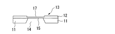
そして、透過膜12の半導体基板2側の面には、その一般面12aと平行な底面17cを有する凹部17が設けられている。
この凹部17は透過膜12の一般面12aに対して略垂直に設けられた周面17aを有しており、その周面17aと底面17cとの稜線が凹部17の周縁部17bとなる。そして、この周縁部17bは、透過孔14の周縁部14bよりも広い範囲で設けられている。
【0017】
ここで、凹部17は周知のガスクラスターイオンビームGCIBの照射によって形成されている。透過膜12の一般面12aの表面粗さはRms=30〜100nm程度であるが、凹部17の底面17cにおいては、ガスクラスターイオンビームGCIBの特性により凹部17の凹加工と同時に底面17cが高精度に平坦化されており、その表面粗さは最良でRms=0.1nmまで平坦化されている。
また、凹部17は0.2〜1.0μmの範囲内で一定の深さとなるように形成されている。凹部17の深さが0.2μmより浅いと、その底面17cに形成される吸収体16が透過膜12の一般面12aから突出し、この発明の効果が低下してしまう。また、1.0μmより深いとメンブレン15の強度が大きく低下してしまう。
【0018】
そして、凹部17の底面17c上であって透過孔14の周縁部14bの内側の範囲には、つまりメンブレン15には、0.2〜0.3μmの厚さを有する吸収体16が形成されている。
この吸収体16は、底面17c上に製膜された吸収膜16aを所望の集積回路パターンに形成してなるものである。吸収膜16aは、底面17cが高精度に平坦化されているため、面粗さによる歪みや残留応力等のストレスが少ない。従って、高集積化された集積回路パターンを形成する場合でも、微細な線幅で正確に形成することが可能となる。
また、凹部17の深さ(図中におけるH)が吸収体16の厚さ(図中におけるT)と同一がそれよりも深く形成されているため、吸収体16の突出上面16bが透過膜12の一般面12aから突出することはない。
尚、吸収膜16aが集積回路パターンに形成される前の状態のデバイスをマスクブランクス10aとする。
【0019】
以上の構成により、半導体基盤2とマスク10とが万が一接触した場合でも、吸収体16が半導体基盤2に先あたりすることがなく、マスク基板11の面上に形成される透過膜12の被支持膜部15a及び吸収体16の突出上面16bが同時に接触するか被支持膜部15aのみが接触するため、メンブレン15が優先的にダメージを受けることがなく、マスク10と半導体基盤2とを狭ギャップ化した場合でもマスク10の破損を回避することができる。
【0020】
また、凹部17が形成されたことにより、メンブレン15が薄膜化されて照射光等の透過率を一層向上させている。更に、凹部17は透過孔14よりも広く形成されているため、露光面積を最大限に設けることができる。そして、凹部17の底面17cが高精度に平坦化されているため、そこに形成される吸収体16の加工前の吸収膜16aの膜質を高めて微細な転写パターンを正確に形成することができる。
【0021】
そして、凹部17の周縁部17bが透過孔14の周縁部14bを避けた位置に形成されているため、メンブレン15に負荷が加わった場合に、透過膜12の一般面12aと凹部17の底面17cとの変化部分での応力集中と、メンブレン15と被支持膜部15aとの境界部分での応力集中とが、同一箇所で生じることを防止することができる。従って、マスク10の破損を回避することができる。
特に、シリコンとダイヤモンドといった熱物性が異なる材料を組み合わせて形成されるダイヤモンドウェハ13においては、その界面11aにストレスが生じているため、透過孔14の周縁部14bの応力集中を低減することの効果が高い。
【0022】
次に、この発明に係るマスク10の製造方法について、X線リソグラフィー用マスクを例に説明する。
先ず、シリコン単結晶から切り出された例えば直径100mm、厚さ2000μmの寸法のマスク基板11を形成する。そして、その上面をRms=0.1〜0.5nmに鏡面加工し、人工ダイヤモンドを蒸着することで、図3に示すように透過膜12(膜厚2μm)を有するダイヤモンドウェハ13を形成する。
【0023】
そして、ダイヤモンドウェハ13の透過膜12の上面であって、透過孔14の周縁部14bよりも広い範囲に、周知のガスクラスターイオンビームGCIBの照射によって0.2〜1.0μmの範囲内で一定の深さを有する凹部17を形成する。
更に、マスク基板11の下面を覆い且つその中央部に50mm×50mmの孔を有する保護シートを密着させ、その孔部分に露出したマスク基板11をエッチング溶液で溶解除去することで、図4に示すように透過孔14及びその透過孔14を覆うメンブレン15を形成する。
【0024】
ここで、ガスクラスターイオンビームGCIBについて図7を用いて説明する。
同図に示すように、ガスクラスターイオンビーム装置50は、主としてクラスター生成部51と、イオン化部52と、加速照射部53とから構成されている。
クラスター生成部51では、アルゴンガス等の原料ガスを高圧で真空中に噴出することにより、原料ガスが断熱膨張により凝縮して原料ガス原子の集団であるクラスター55が生成される。
生成されたクラスター55はイオン化部52でイオン化され、加速照射部53の加速電圧により加速されてガスクラスターイオンビームGCIBとなり被加工物54に照射される。
照射されたガスクラスターイオンビームGCIBは被加工物54に衝突してその加工表面54aをスパッタする。この時、衝突によってクラスター55を形成していた原子が分離し、被加工物54の加工表面54aと平行に飛散することで加工表面54aの突起をスパッタし、加工表面54aが高精度に平坦化される。
【0025】
上記ガスクラスターイオンビームGCIBを用いて人工ダイヤモンドからなる透過膜12に凹部17を形成するに際して、その底面17cの高精度な平坦化を伴う凹加工を行うためのガスクラスターイオンビームGCIBの主要パラメータを下記に示す。
・クラスター生成室圧力:4000〜10000 Torr
・加速電圧:20〜50 Kev
・イオン化電圧:200〜500 V
・イオン化電流:200〜500 mA
・照射量:3e+17〜1e+19 ions/cm2
【0026】
人工ダイヤモンドのような硬い材料に凹部17を形成するにあたって、通常のドライエッチングで加工を行った場合は、凹部17の底面17cの表面粗さが荒くなってしまう。また、機械研磨を行っても凹部17の周縁部17b付近まで研磨することは困難である。
上記のガスクラスターイオンビームGCIBを用いれば、凹部17を形成すると共にその底面17c全域の高精度な平坦化が可能であるため、生産効率が向上すると共に凹部17の底面17cに形成されるX線の吸収膜16aの膜質を高めることができる。
【0027】
上記ガスクラスターイオンビームGCIBの照射によって形成された凹部17の底面17cは、その表面粗さがRms=0.1〜10nmに仕上げられており、図5に示すようにその底面17c上であって透過孔14の周縁部14bの内側の範囲に、つまりメンブレン15に、図示しない反射防止膜を介して、例えばTa膜又はW−Ti合金膜(Ti:1.5%含有)等からなるX線の吸収膜16aを平均膜厚0.2〜0.3μmで製膜し、マスクブランクス10aを形成する。
【0028】
最後に、吸収膜16aの表面に、所望の集積回路パターンを描くように電子ビームを走査させた後にエッチング工程を経て、集積回路パターンを有する吸収体16が形成されて、図6に示すリソグラフィー用のマスク10が完成する。
【0029】
上述のように製造されたリソグラフィー用のマスク10において、ダイヤモンドウェハ13の凹部17をガスクラスターイオンビームGCIBによって形成することにより、凹部17の凹加工とその底面17cの高精度な平坦化加工とを同時に行うことができるため、ダイヤモンドウェハの製造工数を低減できる。
また、短形状の凹部17においても、その底面17cの全域が高精度に平坦化されるため、その面上に形成される吸収膜16aの膜質が高まり、微細な集積回路パターンを正確に形成することができる。
【0030】
【発明の効果】
以上説明してきたように、請求項1に記載した発明によれば、吸収体の、透過膜の被転写体の一般面からの突出量を減少させる又は吸収体の突出を無くすことが可能となるため、マスクと被転写体とをより挟ギャップ化することができる。また、吸収体の配設部位の透過膜をより薄膜化することが可能となるため、照射光等の透過性をより高めることができる。
従って、より高解像の露光が可能となり、半導体装置の一層の高集積化に対応できる効果がある。
【0031】
また、請求項2に記載の発明によれば、マスクに負荷が加わった場合、構造的に最も弱い自立膜部にかかる負荷を低減することが可能となるため、自立膜部の強度を高め、マスクが容易に破損することを防止できる効果がある。
また、マスクの露光面積を最大限に設けることが可能となるため、半導体装置の一層の高集積化に対応できる効果がある。
【0032】
また、請求項3に記載の発明によれば、吸収膜が形成される底面を高精度に平坦化することで吸収体の膜質を高めることが可能となるため、微細な転写パターンを正確に形成することができる効果がある。
【0033】
また、請求項4に記載の発明によれば、凹部の形成とその底面の全域の高精度な平坦化とを同時に行うことが可能となるため、ダイヤモンドウェハの製造工数を低減できる効果がある。
【0034】
また、請求項5に記載の発明によれば、膜質の高い吸収膜を形成することが可能となるため、その吸収膜を所望の転写パターンに形成するに際して、微細な線幅のパターンを正確に形成することができる効果がある。
【0035】
また、請求項6に記載の発明によれば、吸収体の厚さ方向の突出上面が透過膜の被転写体側の一般面と同一かそれよりも突出させないことが可能となるため、万が一マスクと被転写体とが接触した場合に、透過孔の開口範囲に形成されている吸収体の突出上面のみが先あたりすることを防止できる。
従って、強度的に最も弱い自立膜部に負荷が集中することを防止することができ、マスクと被転写体とを挟ギャップ化した場合でもマスクの破損を回避することができる効果がある。
【図面の簡単な説明】
【図1】 本発明の実施形態の斜視説明図である。
【図2】 図1のA−A線に沿う断面図である。
【図3】 ダイヤモンドウェハの加工前の断面図である。
【図4】 ダイヤモンドウェハの加工後の断面図である。
【図5】 マスクブランクスの断面図である。
【図6】 マスクの断面図である。
【図7】 ガスクラスターイオンビーム装置の構成説明図である。
【図8】 従来のX線を露光光源とするステッパの構成説明図である。
【符号の説明】
2 半導体基板
10 マスク
10a マスクブランクス
11 マスク基板
12 透過膜
13 ダイヤモンドウェハ
14 透過孔
14b 周縁部
15 メンブレン
16 吸収体
16a 吸収膜
17 凹部
17b 周縁部
17c 底面
GCIB ガスクラスターイオンビーム[0001]
BACKGROUND OF THE INVENTION
The present invention relates to a diamond wafer, a mask blank and a mask for lithography used for forming an integrated circuit of a semiconductor device, and a method for manufacturing the diamond wafer.
[0002]
[Prior art]
Conventionally, an integrated circuit pattern formed on a mask is transferred to a semiconductor substrate by irradiating a semiconductor substrate, which is a transfer target, with a light beam from an exposure light source through a mask, and the integrated circuit is transferred to the semiconductor substrate through an etching process or the like. Lithographic techniques for forming the are known.
In a stepper (exposure apparatus) used in this technology, an integrated circuit pattern transferred to a semiconductor substrate is usually reduced by reducing an integrated circuit pattern on a mask surface formed by an absorption film for irradiated light through a lens. Is highly integrated.
In recent years, with the further integration of integrated circuits in semiconductor devices, excimer lasers such as KrF laser (wavelength 248 nm) and ArF laser (wavelength 193 nm), electron beams, and X-rays are used to improve transfer resolution. Steppers using an exposure light source having a shorter wavelength such as (wavelength 1 nm) are being put into practical use.
[0003]
In a stepper that uses an exposure light source with a short wavelength as described above, in order to eliminate the decrease in resolution due to diffraction phenomenon such as irradiation light and increase the depth of focus, the lens used in the reduction exposure is abolished and the same magnification exposure is performed. It is possible to accurately perform the exposure of the resolution.
Further, by eliminating the lens, the apparatus can be simplified and the semiconductor substrate can be irradiated without reducing the irradiation area (eg, 50 mm × 50 mm) of the standardized exposure light source, so that the exposure area can be maximized. It can be provided in the limit.
[0004]
Here, as shown in FIG. 8, in the stepper 1 using X-rays as an exposure light source, for example, the
On the other hand, in the
[0005]
The
Then, the semiconductor substrate 2 and the
In this way, by irradiating the semiconductor substrate 2 with a light having a short wavelength through the high-
When the transfer of the integrated circuit pattern to one place on the semiconductor substrate 2 is completed, the
[0006]
[Problems to be solved by the invention]
However, in such a stepper 1 for the same magnification exposure, since the
Further, in order to perform further high-resolution exposure, it is required that the gap between the
Therefore, the present invention provides a high-resolution exposure by sandwiching the mask and a transferred object such as a semiconductor substrate, and avoids damage to the mask even if the mask and the transferred object are in contact. Diamond wafers, mask blanks and masks, and a method for producing a diamond wafer are provided.
[0007]
[Means for Solving the Problems]
In order to solve the above-mentioned problems, the invention described in claim 1 is an object for lithography in which a transmission film of diamond is formed on a surface of a mask substrate having a transmission hole so as to cover the transmission hole. The diamond wafer is characterized in that a concave portion is provided on a surface of the transmissive film on the transfer target side where an absorber such as irradiation light is disposed.
By configuring in this way, the absorber is disposed on the bottom surface of the concave portion at a position lower than the general surface of the permeable membrane on the transfer target side, so that the permeable membrane protrudes from the general surface on the transfer target side. It is possible to reduce the amount or eliminate the protrusion of the absorber. In addition, the permeable membrane at the site where the absorber is disposed can be made thinner.
Here, said irradiation light etc. are the concepts containing an electron beam and an X-ray.
[0008]
The invention described in claim 2 is characterized in that the peripheral edge of the recess is provided in a wider range than the peripheral edge of the transmission hole.
By configuring in this way, the permeable membrane is formed on the surface of the mask substrate and the self-supporting membrane portion composed of only the permeable membrane, the changed portion of the permeable membrane on the transferred material side and the bottom surface of the recess. Since the boundary portion with the supported film portion can be provided at different positions, when a load is applied to the mask, it is possible to reduce the load applied to the self-supporting film portion that is structurally weakest.
In addition, since the bottom surface of the concave portion can be formed wider than the transmission hole that is a transmission portion for irradiation light or the like, the absorber disposed on the bottom surface of the concave portion can be formed to the maximum within the opening range of the transmission hole. Accordingly, it is possible to maximize the exposure area of the mask.
[0009]
According to a third aspect of the present invention, the concave portion is formed by irradiation with a gas cluster ion beam, and the surface roughness of the bottom surface is Rms = 0.1 to 10 nm.
By comprising in this way, the absorption film which is the state before processing of an absorber is on the bottom surface where the surface roughness is flattened with high accuracy up to Rms (root mean square surface roughness) = 0.1 to 10 nm. Since it is formed, it is possible to improve the film quality of the absorption film.
[0010]
According to a fourth aspect of the present invention, there is provided a method for producing a diamond wafer for lithography, comprising: a step of forming a diamond permeable film on a mask substrate; and a step of forming a membrane comprising only the permeable film. A concave portion having a bottom surface with a surface roughness of Rms = 0.1 to 10 nm is formed by irradiation with a gas cluster ion beam on the surface of the transmission film on the side of the transferred body where an absorber such as irradiation light is disposed. Including a process.
By this method, concave processing of a hard material such as diamond is performed, and the fact that the processing surface is flattened with high accuracy as the characteristics of the gas cluster ion beam is used, so that the entire area of the bottom surface of the concave portion is Rms = 0. It is possible to flatten with high accuracy from 1 to 10 nm.
Here, it is desirable that the peripheral shape of the recess has a minimum width in order to shorten the processing step, and therefore, it is desirable that the peripheral shape be a short shape along the peripheral shape of the transmission hole. In this case, since it is difficult to planarize the entire bottom surface of the recess with high accuracy by ordinary dry etching or mechanical polishing, the use of the characteristics of the gas cluster ion beam is particularly effective.
[0011]
Further, the invention described in
With such a configuration, the absorption film can be formed on the bottom surface of the concave portion flattened with high accuracy, and thus it is possible to form an absorption film having a high film quality free from stress due to surface roughness. .
[0012]
According to a sixth aspect of the present invention, there is provided a lithography mask in which an absorption film of the mask blank is formed on an absorber having a desired transfer pattern, wherein the thickness of the absorber is T and the depth of the recess. If H is H, T ≦ H.
By configuring in this way, it is possible to prevent the protruding upper surface in the thickness direction of the absorber formed on the bottom surface of the concave portion of the permeable membrane from being the same as or more than the general surface of the permeable membrane on the transferred material side. It becomes.
[0013]
DETAILED DESCRIPTION OF THE INVENTION
Embodiments of the present invention will be described below with reference to the drawings.
FIG. 1 is a perspective explanatory view of a
As shown in the figure, a
A 50 mm × 50
[0014]
Irradiation formed on the surface of the
In the stepper 1 (not shown), the
[0015]
2 is a cross-sectional view taken along line AA in FIG.
As shown in the figure, the central portion of the
On the surface of the
The ridge line between the
[0016]
A
The
[0017]
Here, the
The
[0018]
An
The
Further, since the depth of the recess 17 (H in the figure) is the same as the thickness of the absorber 16 (T in the figure), it is formed deeper than that. It does not protrude from the
A device in a state before the
[0019]
With the above configuration, even if the semiconductor substrate 2 and the
[0020]
Further, since the
[0021]
Since the
In particular, in the
[0022]
Next, a method for manufacturing the
First, a
[0023]
Then, on the upper surface of the
Furthermore, a protective sheet that covers the lower surface of the
[0024]
Here, the gas cluster ion beam GCIB will be described with reference to FIG.
As shown in the figure, the gas cluster
In the
The generated
The irradiated gas cluster ion beam GCIB collides with the
[0025]
When forming the
-Cluster generation chamber pressure: 4000 to 10000 Torr
・ Acceleration voltage: 20-50 Kev
・ Ionization voltage: 200-500 V
-Ionization current: 200-500 mA
-Irradiation amount: 3e + 17 to 1e + 19 ions / cm 2
[0026]
When the
If the gas cluster ion beam GCIB is used, the
[0027]
The
[0028]
Finally, the surface of the
[0029]
In the
In addition, since the entire
[0030]
【The invention's effect】
As described above, according to the first aspect of the present invention, it is possible to reduce the amount of protrusion of the absorbent body from the general surface of the transfer target body or to eliminate the protrusion of the absorbent body. Therefore, the gap between the mask and the transfer target can be further increased. Moreover, since it is possible to further reduce the thickness of the permeable film at the site where the absorber is disposed, it is possible to further increase the transparency of irradiation light and the like.
Therefore, exposure with higher resolution becomes possible, and there is an effect that it is possible to cope with higher integration of semiconductor devices.
[0031]
Further, according to the invention described in claim 2, when a load is applied to the mask, it is possible to reduce the load applied to the weakest free-standing film portion structurally, thereby increasing the strength of the free-standing film portion, This has the effect of preventing the mask from being easily damaged.
In addition, since the exposure area of the mask can be maximized, there is an effect that the semiconductor device can be further integrated.
[0032]
According to the invention described in
[0033]
According to the fourth aspect of the present invention, it is possible to simultaneously form the concave portion and perform high-precision flattening of the entire area of the bottom surface, so that it is possible to reduce the number of manufacturing steps of the diamond wafer.
[0034]
In addition, according to the invention described in
[0035]
Further, according to the invention described in claim 6, since the upper surface of the absorber in the thickness direction can be made to be the same as or less than the general surface of the permeable membrane on the transfer target side, When the transfer object comes into contact, it can be prevented that only the protruding upper surface of the absorber formed in the opening range of the transmission hole comes first.
Therefore, it is possible to prevent the load from being concentrated on the self-supporting film portion having the weakest strength, and it is possible to avoid damage to the mask even when the gap between the mask and the transfer target is formed.
[Brief description of the drawings]
FIG. 1 is an explanatory perspective view of an embodiment of the present invention.
FIG. 2 is a cross-sectional view taken along the line AA in FIG.
FIG. 3 is a cross-sectional view of a diamond wafer before processing.
FIG. 4 is a cross-sectional view after processing a diamond wafer.
FIG. 5 is a cross-sectional view of a mask blank.
FIG. 6 is a cross-sectional view of a mask.
FIG. 7 is a configuration explanatory diagram of a gas cluster ion beam apparatus.
FIG. 8 is a diagram illustrating the configuration of a conventional stepper that uses an X-ray as an exposure light source.
[Explanation of symbols]
Claims (6)
Priority Applications (1)
| Application Number | Priority Date | Filing Date | Title |
|---|---|---|---|
| JP2002083933A JP3736487B2 (en) | 2002-03-25 | 2002-03-25 | Diamond wafer for lithography, mask blank and mask, and method for manufacturing diamond wafer |
Applications Claiming Priority (1)
| Application Number | Priority Date | Filing Date | Title |
|---|---|---|---|
| JP2002083933A JP3736487B2 (en) | 2002-03-25 | 2002-03-25 | Diamond wafer for lithography, mask blank and mask, and method for manufacturing diamond wafer |
Publications (2)
| Publication Number | Publication Date |
|---|---|
| JP2003282411A JP2003282411A (en) | 2003-10-03 |
| JP3736487B2 true JP3736487B2 (en) | 2006-01-18 |
Family
ID=29231490
Family Applications (1)
| Application Number | Title | Priority Date | Filing Date |
|---|---|---|---|
| JP2002083933A Expired - Fee Related JP3736487B2 (en) | 2002-03-25 | 2002-03-25 | Diamond wafer for lithography, mask blank and mask, and method for manufacturing diamond wafer |
Country Status (1)
| Country | Link |
|---|---|
| JP (1) | JP3736487B2 (en) |
Families Citing this family (6)
| Publication number | Priority date | Publication date | Assignee | Title |
|---|---|---|---|---|
| JP4652946B2 (en) * | 2005-10-19 | 2011-03-16 | Hoya株式会社 | Reflective mask blank substrate manufacturing method, reflective mask blank manufacturing method, and reflective mask manufacturing method |
| JP2007111824A (en) * | 2005-10-20 | 2007-05-10 | Olympus Corp | Method and device for machining workpiece |
| KR20110109563A (en) | 2010-03-31 | 2011-10-06 | 삼성전자주식회사 | How to Correct Optical Parameters for Photo Masks |
| JP2014053073A (en) * | 2012-09-05 | 2014-03-20 | Hitachi High-Technologies Corp | Member for charged particle beam device, charged particle beam device, and barrier membrane member |
| JP5683640B2 (en) * | 2013-05-20 | 2015-03-11 | 日本航空電子工業株式会社 | Cutlery tool |
| EP3363038B1 (en) * | 2015-10-14 | 2022-06-01 | Exogenesis Corporation | Method for ultra-shallow etching using neutral beam processing based on gas cluster ion beam technology |
-
2002
- 2002-03-25 JP JP2002083933A patent/JP3736487B2/en not_active Expired - Fee Related
Also Published As
| Publication number | Publication date |
|---|---|
| JP2003282411A (en) | 2003-10-03 |
Similar Documents
| Publication | Publication Date | Title |
|---|---|---|
| US4393127A (en) | Structure with a silicon body having through openings | |
| US5326426A (en) | Undercut membrane mask for high energy photon patterning | |
| TWI815847B (en) | Mask blank, phase shift mask and method of manufacturing a semiconductor device | |
| TWI594065B (en) | Method of manufacturing multilayer reflection film substrate, method of manufacturing reflective mask base, and method of manufacturing reflective mask | |
| JP2004246366A (en) | Photomask blank, photomask, method and apparatus for manufacturing photomask blank | |
| US7090948B2 (en) | Reflection mask and method for fabricating the reflection mask | |
| KR20040002744A (en) | Method of correcting proximity effect of electronic beam exposure, exposure method, manufacturing method of semiconductor device, and proximity effect correction module | |
| KR100590575B1 (en) | Electron Beam Lithography Method Using New Materials | |
| JP2008311617A (en) | Nano structure, and manufacturing method of nano structure | |
| US6051346A (en) | Process for fabricating a lithographic mask | |
| JP3736487B2 (en) | Diamond wafer for lithography, mask blank and mask, and method for manufacturing diamond wafer | |
| JP3210143B2 (en) | X-ray mask structure, method for manufacturing the same, X-ray exposure method using the X-ray mask structure, and device manufacturing method using the X-ray mask structure | |
| JP2010122304A (en) | Reflective mask blank, reflective mask, method for manufacturing reflective mask blank, and method for manufacturing reflective mask | |
| TWI232495B (en) | Manufacturing method of transfer mask substrate and transfer mask | |
| JP2001326169A (en) | Stencil mask and its manufacturing method | |
| US12050396B2 (en) | Reflective mask blank, method of manufacturing thereof, and reflective mask | |
| JP4066636B2 (en) | Exposure mask, manufacturing method thereof, exposure apparatus and exposure method | |
| US6468700B1 (en) | Transfer mask blanks and transfer masks exhibiting reduced distortion, and methods for making same | |
| US8906582B2 (en) | Blank masks for extreme ultra violet lithography, methods of fabricating the same, and methods of correcting registration errors thereof | |
| JP4346063B2 (en) | Transfer mask blank, transfer mask, and transfer method using the transfer mask | |
| JP2921507B2 (en) | Electron beam exposure mask and method of manufacturing the same | |
| JP2012212787A (en) | Method for manufacturing reflective mask, ion beam device for reflective mask, and reflective mask | |
| US20250036019A1 (en) | Euv reticle with embedded process assistance layer and method of manufacturing the euv reticle | |
| TWI852522B (en) | Blank mask, photomask and manufacturing method of semiconductor device | |
| EP4068000A1 (en) | Conditioning apparatus and method |
Legal Events
| Date | Code | Title | Description |
|---|---|---|---|
| A621 | Written request for application examination |
Free format text: JAPANESE INTERMEDIATE CODE: A621 Effective date: 20040323 |
|
| A977 | Report on retrieval |
Free format text: JAPANESE INTERMEDIATE CODE: A971007 Effective date: 20050706 |
|
| A131 | Notification of reasons for refusal |
Free format text: JAPANESE INTERMEDIATE CODE: A131 Effective date: 20050712 |
|
| A521 | Written amendment |
Free format text: JAPANESE INTERMEDIATE CODE: A523 Effective date: 20050829 |
|
| TRDD | Decision of grant or rejection written | ||
| A01 | Written decision to grant a patent or to grant a registration (utility model) |
Free format text: JAPANESE INTERMEDIATE CODE: A01 Effective date: 20051004 |
|
| A61 | First payment of annual fees (during grant procedure) |
Free format text: JAPANESE INTERMEDIATE CODE: A61 Effective date: 20051017 |
|
| R150 | Certificate of patent or registration of utility model |
Free format text: JAPANESE INTERMEDIATE CODE: R150 |
|
| FPAY | Renewal fee payment (event date is renewal date of database) |
Free format text: PAYMENT UNTIL: 20081104 Year of fee payment: 3 |
|
| FPAY | Renewal fee payment (event date is renewal date of database) |
Free format text: PAYMENT UNTIL: 20091104 Year of fee payment: 4 |
|
| FPAY | Renewal fee payment (event date is renewal date of database) |
Free format text: PAYMENT UNTIL: 20091104 Year of fee payment: 4 |
|
| FPAY | Renewal fee payment (event date is renewal date of database) |
Free format text: PAYMENT UNTIL: 20101104 Year of fee payment: 5 |
|
| FPAY | Renewal fee payment (event date is renewal date of database) |
Free format text: PAYMENT UNTIL: 20101104 Year of fee payment: 5 |
|
| S531 | Written request for registration of change of domicile |
Free format text: JAPANESE INTERMEDIATE CODE: R313531 |
|
| FPAY | Renewal fee payment (event date is renewal date of database) |
Free format text: PAYMENT UNTIL: 20101104 Year of fee payment: 5 |
|
| R350 | Written notification of registration of transfer |
Free format text: JAPANESE INTERMEDIATE CODE: R350 |
|
| FPAY | Renewal fee payment (event date is renewal date of database) |
Free format text: PAYMENT UNTIL: 20111104 Year of fee payment: 6 |
|
| FPAY | Renewal fee payment (event date is renewal date of database) |
Free format text: PAYMENT UNTIL: 20121104 Year of fee payment: 7 |
|
| FPAY | Renewal fee payment (event date is renewal date of database) |
Free format text: PAYMENT UNTIL: 20121104 Year of fee payment: 7 |
|
| FPAY | Renewal fee payment (event date is renewal date of database) |
Free format text: PAYMENT UNTIL: 20131104 Year of fee payment: 8 |
|
| LAPS | Cancellation because of no payment of annual fees |