JP3722116B2 - Reflective electro-optical device and electronic apparatus - Google Patents
Reflective electro-optical device and electronic apparatus Download PDFInfo
- Publication number
- JP3722116B2 JP3722116B2 JP2002366709A JP2002366709A JP3722116B2 JP 3722116 B2 JP3722116 B2 JP 3722116B2 JP 2002366709 A JP2002366709 A JP 2002366709A JP 2002366709 A JP2002366709 A JP 2002366709A JP 3722116 B2 JP3722116 B2 JP 3722116B2
- Authority
- JP
- Japan
- Prior art keywords
- film
- optical device
- electro
- region
- forming layer
- Prior art date
- Legal status (The legal status is an assumption and is not a legal conclusion. Google has not performed a legal analysis and makes no representation as to the accuracy of the status listed.)
- Expired - Lifetime
Links
Images


Classifications
-
- G—PHYSICS
- G02—OPTICS
- G02F—OPTICAL DEVICES OR ARRANGEMENTS FOR THE CONTROL OF LIGHT BY MODIFICATION OF THE OPTICAL PROPERTIES OF THE MEDIA OF THE ELEMENTS INVOLVED THEREIN; NON-LINEAR OPTICS; FREQUENCY-CHANGING OF LIGHT; OPTICAL LOGIC ELEMENTS; OPTICAL ANALOGUE/DIGITAL CONVERTERS
- G02F1/00—Devices or arrangements for the control of the intensity, colour, phase, polarisation or direction of light arriving from an independent light source, e.g. switching, gating or modulating; Non-linear optics
- G02F1/01—Devices or arrangements for the control of the intensity, colour, phase, polarisation or direction of light arriving from an independent light source, e.g. switching, gating or modulating; Non-linear optics for the control of the intensity, phase, polarisation or colour
- G02F1/13—Devices or arrangements for the control of the intensity, colour, phase, polarisation or direction of light arriving from an independent light source, e.g. switching, gating or modulating; Non-linear optics for the control of the intensity, phase, polarisation or colour based on liquid crystals, e.g. single liquid crystal display cells
- G02F1/133—Constructional arrangements; Operation of liquid crystal cells; Circuit arrangements
- G02F1/136—Liquid crystal cells structurally associated with a semi-conducting layer or substrate, e.g. cells forming part of an integrated circuit
- G02F1/1362—Active matrix addressed cells
- G02F1/136286—Wiring, e.g. gate line, drain line
-
- G—PHYSICS
- G02—OPTICS
- G02F—OPTICAL DEVICES OR ARRANGEMENTS FOR THE CONTROL OF LIGHT BY MODIFICATION OF THE OPTICAL PROPERTIES OF THE MEDIA OF THE ELEMENTS INVOLVED THEREIN; NON-LINEAR OPTICS; FREQUENCY-CHANGING OF LIGHT; OPTICAL LOGIC ELEMENTS; OPTICAL ANALOGUE/DIGITAL CONVERTERS
- G02F1/00—Devices or arrangements for the control of the intensity, colour, phase, polarisation or direction of light arriving from an independent light source, e.g. switching, gating or modulating; Non-linear optics
- G02F1/01—Devices or arrangements for the control of the intensity, colour, phase, polarisation or direction of light arriving from an independent light source, e.g. switching, gating or modulating; Non-linear optics for the control of the intensity, phase, polarisation or colour
- G02F1/13—Devices or arrangements for the control of the intensity, colour, phase, polarisation or direction of light arriving from an independent light source, e.g. switching, gating or modulating; Non-linear optics for the control of the intensity, phase, polarisation or colour based on liquid crystals, e.g. single liquid crystal display cells
- G02F1/133—Constructional arrangements; Operation of liquid crystal cells; Circuit arrangements
- G02F1/1333—Constructional arrangements; Manufacturing methods
- G02F1/1335—Structural association of cells with optical devices, e.g. polarisers or reflectors
- G02F1/133553—Reflecting elements
-
- G—PHYSICS
- G02—OPTICS
- G02F—OPTICAL DEVICES OR ARRANGEMENTS FOR THE CONTROL OF LIGHT BY MODIFICATION OF THE OPTICAL PROPERTIES OF THE MEDIA OF THE ELEMENTS INVOLVED THEREIN; NON-LINEAR OPTICS; FREQUENCY-CHANGING OF LIGHT; OPTICAL LOGIC ELEMENTS; OPTICAL ANALOGUE/DIGITAL CONVERTERS
- G02F1/00—Devices or arrangements for the control of the intensity, colour, phase, polarisation or direction of light arriving from an independent light source, e.g. switching, gating or modulating; Non-linear optics
- G02F1/01—Devices or arrangements for the control of the intensity, colour, phase, polarisation or direction of light arriving from an independent light source, e.g. switching, gating or modulating; Non-linear optics for the control of the intensity, phase, polarisation or colour
- G02F1/13—Devices or arrangements for the control of the intensity, colour, phase, polarisation or direction of light arriving from an independent light source, e.g. switching, gating or modulating; Non-linear optics for the control of the intensity, phase, polarisation or colour based on liquid crystals, e.g. single liquid crystal display cells
- G02F1/133—Constructional arrangements; Operation of liquid crystal cells; Circuit arrangements
- G02F1/136—Liquid crystal cells structurally associated with a semi-conducting layer or substrate, e.g. cells forming part of an integrated circuit
- G02F1/1362—Active matrix addressed cells
- G02F1/136227—Through-hole connection of the pixel electrode to the active element through an insulation layer
-
- G—PHYSICS
- G02—OPTICS
- G02F—OPTICAL DEVICES OR ARRANGEMENTS FOR THE CONTROL OF LIGHT BY MODIFICATION OF THE OPTICAL PROPERTIES OF THE MEDIA OF THE ELEMENTS INVOLVED THEREIN; NON-LINEAR OPTICS; FREQUENCY-CHANGING OF LIGHT; OPTICAL LOGIC ELEMENTS; OPTICAL ANALOGUE/DIGITAL CONVERTERS
- G02F1/00—Devices or arrangements for the control of the intensity, colour, phase, polarisation or direction of light arriving from an independent light source, e.g. switching, gating or modulating; Non-linear optics
- G02F1/01—Devices or arrangements for the control of the intensity, colour, phase, polarisation or direction of light arriving from an independent light source, e.g. switching, gating or modulating; Non-linear optics for the control of the intensity, phase, polarisation or colour
- G02F1/13—Devices or arrangements for the control of the intensity, colour, phase, polarisation or direction of light arriving from an independent light source, e.g. switching, gating or modulating; Non-linear optics for the control of the intensity, phase, polarisation or colour based on liquid crystals, e.g. single liquid crystal display cells
- G02F1/133—Constructional arrangements; Operation of liquid crystal cells; Circuit arrangements
- G02F1/1333—Constructional arrangements; Manufacturing methods
- G02F1/1335—Structural association of cells with optical devices, e.g. polarisers or reflectors
- G02F1/133553—Reflecting elements
- G02F1/133555—Transflectors
-
- G—PHYSICS
- G02—OPTICS
- G02F—OPTICAL DEVICES OR ARRANGEMENTS FOR THE CONTROL OF LIGHT BY MODIFICATION OF THE OPTICAL PROPERTIES OF THE MEDIA OF THE ELEMENTS INVOLVED THEREIN; NON-LINEAR OPTICS; FREQUENCY-CHANGING OF LIGHT; OPTICAL LOGIC ELEMENTS; OPTICAL ANALOGUE/DIGITAL CONVERTERS
- G02F1/00—Devices or arrangements for the control of the intensity, colour, phase, polarisation or direction of light arriving from an independent light source, e.g. switching, gating or modulating; Non-linear optics
- G02F1/01—Devices or arrangements for the control of the intensity, colour, phase, polarisation or direction of light arriving from an independent light source, e.g. switching, gating or modulating; Non-linear optics for the control of the intensity, phase, polarisation or colour
- G02F1/13—Devices or arrangements for the control of the intensity, colour, phase, polarisation or direction of light arriving from an independent light source, e.g. switching, gating or modulating; Non-linear optics for the control of the intensity, phase, polarisation or colour based on liquid crystals, e.g. single liquid crystal display cells
- G02F1/133—Constructional arrangements; Operation of liquid crystal cells; Circuit arrangements
- G02F1/1333—Constructional arrangements; Manufacturing methods
- G02F1/1335—Structural association of cells with optical devices, e.g. polarisers or reflectors
- G02F1/13356—Structural association of cells with optical devices, e.g. polarisers or reflectors characterised by the placement of the optical elements
- G02F1/133565—Structural association of cells with optical devices, e.g. polarisers or reflectors characterised by the placement of the optical elements inside the LC elements, i.e. between the cell substrates
-
- G—PHYSICS
- G02—OPTICS
- G02F—OPTICAL DEVICES OR ARRANGEMENTS FOR THE CONTROL OF LIGHT BY MODIFICATION OF THE OPTICAL PROPERTIES OF THE MEDIA OF THE ELEMENTS INVOLVED THEREIN; NON-LINEAR OPTICS; FREQUENCY-CHANGING OF LIGHT; OPTICAL LOGIC ELEMENTS; OPTICAL ANALOGUE/DIGITAL CONVERTERS
- G02F1/00—Devices or arrangements for the control of the intensity, colour, phase, polarisation or direction of light arriving from an independent light source, e.g. switching, gating or modulating; Non-linear optics
- G02F1/01—Devices or arrangements for the control of the intensity, colour, phase, polarisation or direction of light arriving from an independent light source, e.g. switching, gating or modulating; Non-linear optics for the control of the intensity, phase, polarisation or colour
- G02F1/13—Devices or arrangements for the control of the intensity, colour, phase, polarisation or direction of light arriving from an independent light source, e.g. switching, gating or modulating; Non-linear optics for the control of the intensity, phase, polarisation or colour based on liquid crystals, e.g. single liquid crystal display cells
- G02F1/133—Constructional arrangements; Operation of liquid crystal cells; Circuit arrangements
- G02F1/136—Liquid crystal cells structurally associated with a semi-conducting layer or substrate, e.g. cells forming part of an integrated circuit
- G02F1/1362—Active matrix addressed cells
- G02F1/136213—Storage capacitors associated with the pixel electrode
-
- G—PHYSICS
- G02—OPTICS
- G02F—OPTICAL DEVICES OR ARRANGEMENTS FOR THE CONTROL OF LIGHT BY MODIFICATION OF THE OPTICAL PROPERTIES OF THE MEDIA OF THE ELEMENTS INVOLVED THEREIN; NON-LINEAR OPTICS; FREQUENCY-CHANGING OF LIGHT; OPTICAL LOGIC ELEMENTS; OPTICAL ANALOGUE/DIGITAL CONVERTERS
- G02F2201/00—Constructional arrangements not provided for in groups G02F1/00 - G02F7/00
- G02F2201/48—Flattening arrangements
Landscapes
- Physics & Mathematics (AREA)
- Nonlinear Science (AREA)
- Mathematical Physics (AREA)
- Chemical & Material Sciences (AREA)
- Crystallography & Structural Chemistry (AREA)
- General Physics & Mathematics (AREA)
- Optics & Photonics (AREA)
- Engineering & Computer Science (AREA)
- Microelectronics & Electronic Packaging (AREA)
- Liquid Crystal (AREA)
- Devices For Indicating Variable Information By Combining Individual Elements (AREA)
- Thin Film Transistor (AREA)
Description
【0001】
【発明の属する技術分野】
本発明は、反射型電気光学装置、およびそれを用いた電子機器に関するものである。さらに詳しくは、反射型電気光学装置の画素構成に関するものである。
【0002】
【従来の技術】
液晶装置などの電気光学装置は、各種機器の直視型の表示装置として用いられている。このような電気光学装置のうち、例えば、画素スイッチング用の非線形素子としてTFTを用いたアクティブマトリクス型の液晶装置では、図25および図26に示すように、電気光学物質としての液晶50を挟持するTFTアレイ基板10および対向基板20のうち、TFTアレイ基板10の方には、画素スイッチング用のTFT(薄膜トランジスタ/Thin Film Transistor)30と、このTFT30に電気的に接続するITO膜などの透明導電膜からなる画素電極9aとが形成されている。
【0003】
また、液晶装置のうち、反射型のものでは、対向基板20の側から入射してきた外光を対向基板20の方に向けて反射するための光反射膜8aが画素電極9aの下層側に形成されており、対向基板20側から入射した光をTFTアレイ基板10側で反射し、対向基板20側から出射された光によって画像を表示する(反射モード)。
【0004】
但し、反射型の液晶装置において、光反射膜8aで反射された光の方向性が強いと、画像をみる角度で明るさが異なるなどの視野角依存性が顕著に出てしまう。そこで、液晶装置を製造する際、層間絶縁膜4、あるいはその表面に形成した表面保護膜14の表面に、アクリル樹脂などといった感光性樹脂を塗布した後、フォトリソグラフィ技術を用いて、凹凸形成層13aを形成することにより、光反射膜8aの表面に光散乱用の凹凸パターン8gを付与している。
【0005】
ここに示す例では、図27に示すように、感光性樹脂13に対して露光マスク200を介してハーフ露光し、感光性樹脂13の厚さ方向の途中まで感光させた後、現像し、さらに加熱して感光性樹脂13を溶融させることにより、なだらかな膜厚変化に対応する凹凸を表面に備えた凹凸形成層13aを形成したので、凹凸形成層13aの上層に直接、光反射膜8aを形成してある。
【0006】
すなわち、感光性樹脂13にハーフ露光を行うと、感光性樹脂13は、厚さ方向の途中位置まで露光されるだけであるため、感光性樹脂13を現像すると、露光された部分は凹部13bが形成される一方、露光されなかった部分は厚いままである。従って、感光性樹脂13を現像した後、感光性樹脂13に対して加熱処理を行って、感光性樹脂13を溶融させると、感光性樹脂13は、膜厚がなだらかに変化し、この膜厚変化に対応して、表面になだらかな凹凸を備えた凹凸形成層13aとなる。従って、凹凸形成層13aの上層に直接、光反射膜8aを形成しても、光反射膜8aの表面には、エッジのない、なだらかな凹凸パターン8gが付与される。
【0007】
【発明が解決しようとする課題】
しかしながら、従来の液晶装置では、凹凸形成層13aの下層側に、各種配線やTFT30を構成する導電膜、例えば、走査線3a、容量線3b、データ線6a、ドレイン電極6bなどが形成されているため、それらを構成する導電膜の有無によって高低差が形成されている。すなわち、画素領域内に、半導体膜1aの延設部分1f、容量線3b、ドレイン電極6bが多層に形成されている第1領域10aと、ドレイン電極6bは形成されているが、半導体膜1aの延設部分1fや容量線3bが形成されていない第2領域10bと、半導体膜1aの延設部分1f、容量線3b、ドレイン電極6bのいずれもが形成されていない第3領域10cとが存在し、これらの各領域には、導電膜の形成層数の差に相当する高低差がある。このため、図27に示すように、感光性樹脂13に対する露光を行う際、段差の高所部分と低所部分との間では光源からの距離が相違するため、フォーカスずれが発生し、露光ムラが発生するという問題点がある。
【0008】
また、感光性樹脂13に対する露光を行う際、下層側に導電膜がある領域(第1領域10a、第2領域10b)と、下層側に導電膜がない領域(第3領域10c)との間には導電膜からの反射光の有無や強度に起因する露光ムラが発生するという問題点がある。
【0009】
このような露光ムラが発生すると、低所部分では、凹凸形成層13aの凹部13bが浅くなってしまうなど、凹凸形成層13aを目論見どおりに形成できず、光反射膜8aの表面に所望の凹凸パターンを形成できないので、好ましくない。
【0010】
なお、凹凸形成層13aを完全露光して凹凸形成層13aを所定パターンで残し、凹凸形成層13aの有無によって光反射膜8aの表面に凹凸パターン8gを付与する場合があり、このような場合には、凹凸形成層13aにエッジが発生するので、凹凸形成層13aの上層にもう1層、流動性の高い感光性樹脂層からなる上層絶縁膜を塗布、形成した後、その上層側に光反射膜8aを形成するが、このような場合でも、凹凸形成層13aの下層側に高低差があると、露光ムラが発生する。
【0011】
また、高低差がある領域に感光性樹脂を塗布すると、図27に示すように、平坦化作用によって高い領域には感光性樹脂が薄く形成される一方、低い領域には感光性樹脂が厚く形成される。このため、露光および現像の後、感光性樹脂13を加熱、溶融させて、なだらかな凹凸を表面に備えた凹凸形成層13aを形成する際、高い領域では感光性樹脂が薄いため、樹脂の垂れが小さいので、比較的大きな凹凸が形成される。これに対して、低い領域では感光性樹脂が厚いため、樹脂の垂れが大きいので、凹凸が小さくなってしまい、凹凸の大きさがばらつくという問題点がある。
【0012】
以上の問題点に鑑みて、本発明の課題は、凹凸形成層の下層側の状態を均一化しておくことにより、フォトリグラフィ技術を利用して凹凸形成層を形成する際に、凹凸形状にばらつきが発生しない反射型電気光学装置、および電子機器を提供することにある。併せて、反射領域の段差解消により、反射部セルギャップ均一性が向上し、コントラスト等の表示品位を向上できる反射型電気光学装置、および電子機器を提供することにある。
【0013】
【課題を解決するための手段】
上記課題を解決するため、本発明では、電気光学物質を挟持する基板上には、各画素毎に少なくとも、一つ又は複数の配線に電気的に接続する画素スイッチング用のアクティブ素子と、光反射膜とを有し、該光反射膜の下層側のうち、当該光反射膜と平面的に重なる領域に、前記光反射膜の表面に所定の凹凸パターンを付与する凹凸形成層が形成された反射型電気光学装置において、前記凹凸形成層の下層側で当該凹凸形成層と平面的に重なる領域のうち、前記アクティブ素子を構成する導電膜が配置されていない領域には、前記アクティブ素子を形成する導電膜の有無によって形成される高低差を解消するための高低差解消膜が形成され、当該高低差解消膜は、前記配線を構成する導電膜、前記アクティブ素子を構成する導電膜、および絶縁膜のうちの少なくとも一層から形成されてなることを特徴とする。
【0014】
反射型の電気光学装置において、各種配線やアクティブ素子を構成する導電膜の形成層数に差があると、その膜厚に相当する高低差、段差が形成されるが、本発明では、導電膜の形成層数が少ない領域に高低差解消膜が形成されており、この高低差解消膜によって、凹凸形成層の下層側では高低差、高低差が解消されている。従って、感光性樹脂に対する露光を行って凹凸形成層を形成する際、高所部分と低所部分との間に顕著な高低差がないため、露光ムラが発生しない。また、高低差がある領域に感光性樹脂を塗布すると、高い領域には感光性樹脂が薄く形成される一方、低い領域には感光性樹脂が厚く形成されるため、露光および現像の後、感光性樹脂を加熱、溶融させて、なだらかな凹凸を表面に備えた凹凸形成層を形成する際、高い領域では感光性樹脂が薄いため、樹脂の垂れが小さいので、比較的大きな凹凸が形成される傾向にあるが、本発明では、このような問題も解消することができる。それ故、凹凸形成層を目論見どおりに形成できるので、光反射膜の表面に所望の凹凸パターンを形成することができる。また、高低差解消膜は、配線を構成する導電膜、アクティブ素子を構成する導電膜、あるいは絶縁膜から形成されているため、高低差解消膜を形成するにあたって製造工程を追加する必要がない。さらに、画素電極の下層側に高低差があると液晶などの電気光学物質層の層厚が領域毎に異なることになるが、本発明では、高低差が解消されているので、表示品位が向上するという利点もある。
【0015】
本発明において、前記高低差解消膜は、前記配線を構成する導電膜、前記アクティブ素子を構成する導電膜、および絶縁膜のうちの少なくとも一層から形成されてなることが好ましい。このように構成すると、導電膜が存在する領域と、存在しない領域とがあって、露光の際、導電膜から反射してくる光の有無や強度ばらつきによって露光ムラが発生する傾向にあっても、本発明では、画素の略全体にわたって導電膜が形成されているので、露光ムラが発生しない。また、導電膜が存在する領域と、存在しない領域とでは、熱の伝達性に差があって、温度ばらつきが発生しやすいが、導電膜を略全体に形成しておけば、温度ばらつきを圧縮できるので、感光性樹脂の硬化速度を均一化できる。それ故、凹凸形成層を目論見どおりに形成できるので、光反射膜の表面に所望の凹凸パターンを形成することができる。また、高低差解消膜は、配線、あるいはアクティブ素子を構成する導電膜と同層に形成されているため、高低差解消膜を形成するにあたって製造工程を追加する必要がない。
【0016】
本発明において、前記高低差解消膜は、例えば、前記アクティブ素子を形成する導電膜の形成層数が少ない領域に対して選択的に形成されていることにより、前記高低差を解消している。
【0017】
本発明において、前記アクティブ素子が前記配線としての走査線およびデータ線に接続する薄膜トランジスタである場合には、前記高低差解消膜として、例えば、前記走査線と同層に同時形成された導電膜、あるいは前記データ線と同層に同時形成された導電膜のうちの少なくとも一方が形成される。
【0018】
また、本発明において、前記アクティブ素子が前記配線としての走査線およびデータ線に接続する薄膜トランジスタであり、かつ、前記画素には蓄積容量を構成するための容量線が通っている場合には、前記高低差解消膜として、例えば、前記走査線と同層の導電膜、前記容量線と同層の導電膜、あるいは前記データ線と同層の導電膜のうちの少なくとも一層が形成される。
【0019】
本発明において、前記高低差解消膜は、前記配線、あるいは前記アクティブ素子を構成する導電膜から分離して島状に形成されていることが好ましい。このように構成すると、他の層と高低差解消膜が平面的に重なっている領域に寄生容量が発生するのを防止することができる。
【0020】
また、本発明において、前記高低差解消膜は、前記配線、あるいは前記アクティブ素子を構成する導電膜から延設されている構成であってもよい。例えば、容量部の上電極を延設して前記高低差解消膜とする構成であってもよい。
【0021】
さらに本発明の別の形態では、電気光学物質を挟持する基板上には、各画素毎に少なくとも、一つ又は複数の配線に電気的に接続する画素スイッチング用のアクティブ素子と、光反射膜とが形成され、該光反射膜の下層側で当該光反射膜と平面的に重なる領域には前記光反射膜の表面に所定の凹凸パターンを付与する凹凸形成層が形成された反射型電気光学装置において、前記凹凸形成層の下層側で当該凹凸形成層と平面的に重なる領域のうち、前記アクティブ素子を構成する導電膜が配置されていない領域には、電気的に他の領域から絶縁された島状パターンが形成され、該島状パターンは、前記配線を構成する導電膜、および前記アクティブ素子を構成する導電膜のうちの少なくとも一層から形成されてなることを特徴とする。
【0022】
本発明において、前記凹凸形成層が、なだらかな膜厚変化に対応する凹凸を表面に備えた感光性樹脂からなる場合があり、この場合には、前記光反射膜の表面には、前記凹凸形成層の表面に形成された凹凸が反映されて前記凹凸パターンが形成される。このような形態は、感光性樹脂に対する露光マスクを介してのハーフ露光、および現像によって前記凹凸形成層を形成することにより実現できる。
【0023】
本発明において、前記凹凸形成層は、所定のパターンに選択的に形成された感光性樹脂からなる場合があり、この場合には、前記光反射膜の表面には、前記凹凸形成層の有無に対応して前記凹凸パターンが形成される。このような形態は、感光性樹脂に対する露光マスクを介しての露光、および現像によって前記凹凸形成層を形成することにより実現できる。
【0024】
ここで、凹凸形成層にエッジがある場合には、前記凹凸形成層の上層に上層絶縁膜を形成する。このように構成すると、前記光反射膜の表面には、前記凹凸形成層が構成する凹凸が当該上層絶縁膜を介して反映されて前記凹凸パターンが形成されることになる。
【0025】
本発明において、電気光学装置を全反射型として構成する場合には、前記凹凸形成層は、前記画素の略全域にわたって形成されることになる。
【0026】
これに対して、本発明に係る電気光学装置を半透過・反射型として構成する場合には、前記光反射膜に光透過窓を形成した構成とすればよい。この場合、光透過率の低下を防ぐために、前記光透過窓の領域に前記高低差解消膜、あるいは前記島状パターンを形成しないことが望ましい。このように構成すると、光透過窓の領域で露光ムラがあったとしても、この領域には感光性樹脂による凹凸形状を形成する必要がないので、何ら問題は生じない。
【0027】
本発明において、前記電気光学物質は、例えば、液晶である。
【0028】
本発明を適用した電気光学装置は、モバイルコンピュータや携帯電話機などといった電子機器の表示装置として用いることができる。
【0029】
【発明の実施の形態】
図面を参照して、本発明の実施の形態を説明する。
【0030】
[実施の形態1]
(反射型電気光学装置の基本的な構成)
図1は、本発明を適用した電気光学装置を各構成要素とともに対向基板の側から見た平面図であり、図2は、図1のH−H′断面図である。図3は、電気光学装置の画像表示領域においてマトリクス状に形成された複数の画素における各種素子、配線等の等価回路図である。なお、本形態の説明に用いた各図では、各層や各部材を図面上で認識可能な程度の大きさとするため、各層や各部材毎に縮尺を異ならしめてある。
【0031】
図1および図2において、本形態の反射型の電気光学装置100は、シール材52によって貼り合わされたTFTアレイ基板10と対向基板20との間に、電気光学物質としての液晶50が挟持されており、シール材52の形成領域の内側領域には、遮光性材料からなる周辺見切り53が形成されている。シール材52の外側の領域には、データ線駆動回路101、および実装端子102がTFTアレイ基板10の一辺に沿って形成されており、この一辺に隣接する2辺に沿って走査線駆動回路104が形成されている。TFTアレイ基板10の残る一辺には、画像表示領域の両側に設けられた走査線駆動回路104の間をつなぐための複数の配線105が設けられており、更に、周辺見切り53の下などを利用して、プリチャージ回路や検査回路が設けられることもある。また、対向基板20のコーナー部の少なくとも1箇所においては、TFTアレイ基板10と対向基板20との間で電気的導通をとるための上下導通材106が形成されている。
【0032】
なお、データ線駆動回路101および走査線駆動回路104をTFTアレイ基板10の上に形成する代わりに、たとえば、駆動用LSIが実装されたTAB(テープ オートメイテッド、ボンディング)基板をTFTアレイ基板10の周辺部に形成された端子群に対して異方性導電膜を介して電気的および機械的に接続するようにしてもよい。なお、電気光学装置100では、使用する液晶50の種類、すなわち、TN(ツイステッドネマティック)モード、STN(スーパーTN)モード等々の動作モードや、ノーマリホワイトモード/ノーマリブラックモードの別に応じて、偏光フィルム、位相差フィルム、偏光板などが所定の向きに配置されるが、ここでは図示を省略してある。また、電気光学装置100をカラー表示用として構成する場合には、対向基板20において、TFTアレイ基板10の各画素電極(後述する。)に対向する領域にRGBのカラーフィルタをその保護膜とともに形成する。
【0033】
このような構造を有する電気光学装置100の画像表示領域10aにおいては、図3に示すように、複数の画素100aがマトリクス状に構成されているとともに、これらの画素100aの各々には、画素電極9a、およびこの画素電極9aを駆動するための画素スイッチング用のTFT30が形成されており、画素信号S1、S2・・・Snを供給するデータ線6aが当該TFT30のソースに電気的に接続されている。データ線6aに書き込む画素信号S1、S2・・・Snは、この順に線順次に供給しても構わないし、相隣接する複数のデータ線6a同士に対して、グループ毎に供給するようにしてもよい。また、TFT30のゲートには走査線3aが電気的に接続されており、所定のタイミングで、走査線3aにパルス的に走査信号G1、G2・・・Gmをこの順に線順次で印加するように構成されている。画素電極9aは、TFT30のドレインに電気的に接続されており、スイッチング素子であるTFT30を一定期間だけそのオン状態とすることにより、データ線6aから供給される画素信号S1、S2・・・Snを各画素に所定のタイミングで書き込む。このようにして画素電極9aを介して液晶に書き込まれた所定レベルの画素信号S1、S2、・・・Snは、図2に示す対向基板20の対向電極21との間で一定期間保持される。
【0034】
ここで、液晶50は、印加される電圧レベルにより分子集合の配向や秩序が変化することにより、光を変調し、階調表示を可能にする。ノーマリーホワイトモードであれば、印加された電圧に応じて入射光がこの液晶50の部分を通過する光量が低下し、ノーマリーブラックモードであれば、印加された電圧に応じて入射光がこの液晶50の部分を通過する光量が増大していく。その結果、全体として電気光学装置100からは画素信号S1、S2、・・・Snに応じたコントラストを持つ光が出射される。
【0035】
なお、保持された画素信号S1、S2、・・・Snがリークするのを防ぐために、画素電極9aと対向電極との間に形成される液晶容量と並列に蓄積容量60を付加することがある。このような構成を採用することにより、画素電極9aの電圧は、例えば、ソース電圧が印加された時間よりも3桁も長い時間だけ蓄積容量60により保持される。これにより、電荷の保持特性は改善され、コントラスト比の高い電気光学装置100が実現できる。なお、蓄積容量60を形成する方法としては、図3に例示するように、蓄積容量60を形成するための配線である容量線3bとの間に形成する場合、あるいは前段の走査線3aとの間に形成する場合もいずれであってもよい。
【0036】
(TFTアレイ基板の構成)
図4は、本形態の電気光学装置に用いたTFTアレイ基板の相隣接する複数の画素群の平面図である。図5は、図4に示すTFTアレイ基板の画素群から走査線、データ線、容量線などの配線、およびTFT30を構成する導電膜のみを抜き出して示す平面図であり、この図では、本形態の特徴的な部分を太線で示してある。図6は、電気光学装置の画素の一部を図4のA−A′線に相当する位置で切断したときの断面図である。
【0037】
図4および図5において、TFTアレイ基板10上には、複数の透明なITO(Indium Tin Oxide)膜からなる画素電極9aがマトリクス状に形成されており、これら各画素電極9aに対して画素スイッチング用のTFT30がそれぞれ接続している。また、画素電極9aの縦横の境界に沿って、データ線6a、走査線3a、および容量線3bが形成され、TFT30は、データ線6aおよび走査線3aに対して接続している。すなわち、データ線6aは、コンタクトホール15を介してTFT30の高濃度ソース領域1dに電気的に接続し、走査線3aは、その突出部分がTFT30のゲート電極を構成している。なお、蓄積容量60は、画素スイッチング用のTFT30を形成するための半導体膜1の延設部分1fを導電化したものを下電極とし、この下電極41に容量線3bが上電極として重なった構造になっている。
【0038】
このように構成した画素領域のA−A′線における断面は、図6に示すように、TFTアレイ基板10の基体たる透明な基板10′の表面に、厚さが300nm〜500nmのシリコン酸化膜(絶縁膜)からなる下地保護膜11が形成され、この下地保護膜11の表面には、厚さが30nm〜100nmの島状の半導体膜1aが形成されている。半導体膜1aの表面には、厚さが約50〜150nmのシリコン酸化膜からなるゲート絶縁膜2が形成され、このゲート絶縁膜2の表面に、厚さが300nm〜800nmの走査線3aが形成されている。半導体膜1aのうち、走査線3aに対してゲート絶縁膜2を介して対峙する領域がチャネル領域1a′になっている。このチャネル領域1a′に対して一方側には、低濃度ソース領域1bおよび高濃度ソース領域1dを備えるソース領域が形成され、他方側には、低濃度ドレイン領域1cおよび高濃度ドレイン領域1eを備えるドレイン領域が形成されている。
【0039】
走査線3aの表面側には、厚さが300nm〜800nmのシリコン酸化膜からなる層間絶縁膜4が形成されている。層間絶縁膜4の表面には、厚さが300nm〜800nmのデータ線6aが形成され、このデータ線6aは、層間絶縁膜4に形成されたコンタクトホール15を介して高濃度ソース領域1dに電気的に接続している。層間絶縁膜4の表面にはデータ線6aと同時形成されたドレイン電極6bが形成され、このドレイン電極6bは、層間絶縁膜4に形成されたコンタクトホール16を介して高濃度ドレイン領域1eに電気的に接続している。また、データ線6aおよびドレイン電極6bの表面には、厚さが100nm〜300nmのシリコン窒化膜からなる表面保護膜14が形成されている。
【0040】
表面保護膜14の表面には、透光性の感光性樹脂からなる凹凸形成層13aが形成されている。また、凹凸形成層13aの表面には、アルミニウム膜などからなる光反射膜8aが形成されている。従って、光反射膜8aの表面には、凹凸形成層13aが構成する凹凸が反映されて凹凸パターン8gが形成されている。
【0041】
また、光反射膜8aの上層にはITO膜からなる画素電極9aが形成されている。画素電極9aは、光反射膜8aの表面に直接、積層され、画素電極9aと光反射膜8aとは電気的に接続されている。また、画素電極9aは、凹凸形成層13a、表面保護膜14、および層間絶縁膜4に形成されたコンタクトホール17を介してドレイン電極6bに電気的に接続している。
【0042】
ここで、ドレイン電極6bは、TFT30の高濃度ソース領域1eと重なる位置から容量線3bと交差して画素領域の略中央にまで延びており、ドレイン電極6bと画素電極9aは、画素領域の略中央でコンタクトホール17を介して電気的に接続している。
【0043】
画素電極9aの表面側にはポリイミド膜からなる配向膜12が形成されている。この配向膜12は、ポリイミド膜に対してラビング処理が施された膜である。
【0044】
なお、高濃度ドレイン領域1eからの延設部分1f(下電極)に対しては、ゲート絶縁膜2aと同時形成された絶縁膜(誘電体膜)を介して容量線3bが上電極として対向することにより、蓄積容量60が構成されている。
【0045】
なお、TFT30は、好ましくは上述のようにLDD構造をもつが、低濃度ソース領域1b、および低濃度ドレイン領域1cに相当する領域に不純物イオンの打ち込みを行わないオフセット構造を有していてもよい。また、TFT30は、ゲート電極(走査線3aの一部)をマスクとして高濃度で不純物イオンを打ち込み、自己整合的に高濃度のソースおよびドレイン領域を形成したセルフアライン型のTFTであってもよい。
【0046】
また、本形態では、TFT30のゲート電極(走査線3a)をソース−ドレイン領域の間に1個のみ配置したシングルゲート構造としたが、これらの間に2個以上のゲート電極を配置してもよい。この際、各々のゲート電極には同一の信号が印加されるようにする。このようにデュアルゲート(ダブルゲート)、あるいはトリプルゲート以上でTFT30を構成すれば、チャネルとソース−ドレイン領域の接合部でのリーク電流を防止でき、オフ時の電流を低減することが出来る。これらのゲート電極の少なくとも1個をLDD構造或いはオフセット構造にすれば、さらにオフ電流を低減でき、安定したスイッチング素子を得ることができる。
【0047】
(凹凸パターンの詳細構成)
図6に示すように、TFTアレイ基板10において、光反射膜8aの表面には、凸部8bおよび凹部8cを備えた凹凸パターン8gが形成されており、本形態では、図4に示すように、凹部8c、およびそれを構成する凹凸形成層13aの凹部13bを円形の平面形状で表してある。但し、凹部8c、および凹凸形成層13aの凹部13bの平面形状については、円角に限らず、楕円形や角形など、種々の形状のものを採用することができる。
【0048】
このような凹凸パターン8gを構成するにあたって、本形態のTFTアレイ基板10では、光反射膜8aの下層側のうち、凹凸パターン8gの凸部8bに相当する領域には、透光性の感光性樹脂13からなる凹凸形成層13aが厚く形成されている一方、凹部8cに相当する領域には、凹凸形成層13aの薄い凹部13bが形成され、その上層側に形成される光反射膜8aの表面に光散乱用の凹凸パターン8gを付与している。
【0049】
ここで、凹凸形成層13aは、表面はエッジのない、なだらかな形状になっている。このため、凹凸形成層13aの上層に光反射膜8aを直接、積層しても、光反射膜8aの表面にはエッジのない、なだらかな形状の凹凸パターン8gが形成されている。
【0050】
このような凹凸形成層13aは、後述するように、ポジタイプの感光性樹脂13を塗布した後、この感光性樹脂13に対して、露光マスクを介してのハーフ露光、現像、および加熱を行ったものである。従って、凹凸パターン8gの凹部8cに相当する領域では、凹凸形成層13aを構成する感光性樹脂13が厚さ方向の途中位置まで露光、現像される結果、感光性樹脂13が完全に除去されずに薄く残った凹部13bになっている。これに対して、凹凸パターン8gの凸部8bに相当する領域では、凹凸形成層13aを構成する感光性樹脂13が露光されず、厚いまま残っている。また、ハーフ露光、現像した後の感光性樹脂13に対しては加熱処理が施されているため、この加熱処理によって、感光性樹脂13が溶融する結果、凹凸形成層13aは、角張った部分がなく、エッジのない、なだらかな形状になっている。
【0051】
ここで、TFTアレイ基板10では、画素100a内に、半導体膜1aの延設部分1f、容量線3b、ドレイン電極6bが多層に形成されている第1領域10aと、ドレイン電極6bは形成されているが、半導体膜1aの延設部分1fや容量線3bが形成されていない第2領域10bと、半導体膜1aの延設部分1f、容量線3b、ドレイン電極6bのいずれもが形成されていない第3領域10cとが存在し、これらの領域のうち、第3領域10cには、容量線3bや走査線3bと同層の高低差解消膜3fが2箇所、島状に形成されている。すなわち、本形態では、容量線3bを挟む両側2箇所(容量線3bおよびドレイン電極6bのいずれもが形成されていない領域)に高低差解消膜3fが形成されている。このため、容量線3bおよびドレイン電極6bの有無に起因する高低差は、高低差解消膜3fによって解消されている。また、第1領域10aと、第2領域10bおよび第3領域10cとは、半導体膜1a(延設部分1f)の膜厚に相当する高低差しかなく、この高低差は著しく小さいので、第1領域10a、第2領域10b、および第3領域10cには高低差がほとんどない。
【0052】
(対向基板の構成)
なお、対向基板20では、TFTアレイ基板10に形成されている画素電極9aの縦横の境界領域と対向する領域にブラックマトリクス、あるいはブラックストライプなどと称せられる遮光膜23が形成され、その上層側には、ITO膜からなる対向電極21が形成されている。また、対向電極21の上層側には、ポリイミド膜からなる配向膜22が形成され、この配向膜22は、ポリイミド膜に対してラビング処理が施された膜である。
【0053】
(本形態の作用・効果)
このように構成した半透過・反射型の電気光学装置100では、画素電極9aの下層側に光反射膜8aが形成されているため、対向基板20側から入射した光をTFTアレイ基板10側で反射し、対向基板20側から出射された光によって画像を表示する(反射モード)。
【0054】
ここで、TFTアレイ基板10では、走査線3aと同層の容量線3b並びにゲート電極、TFT30を構成する半導体膜1a、その延設部分1f、データ線6aと同層のドレン電極6bが選択的に形成されているため、これらの導電膜の形成層数に差があると、その膜厚に相当する高低差が形成される。しかるに本形態では、導電膜の形成層数が少ない領域、すなわち、第3領域10cには、走査線3aおよび容量線3bと同層の高低差解消膜3fが形成され、この高低差解消膜3fによって、凹凸形成層13aの下層側では高低差が解消されている。従って、後述する工程において、感光性樹脂13に対する露光を行って凹凸形成層13aを形成する際、第1領域10a、第2領域10b、および第3領域10cのいずれの領域においても、感光性樹脂13に対して露光ムラが発生しない。
【0055】
また、高低差がある領域に感光性樹脂13を塗布すると、高い領域には感光性樹脂13が薄く形成される一方、低い領域には感光性樹脂13が厚く形成される。このため、露光および現像の後、感光性樹脂を加熱、溶融させて、なだらかな凹凸を表面に備えた凹凸形成層13aを形成する際、高い領域では感光性樹脂13が薄いため、樹脂の垂れが小さいので、比較的大きな凹凸が形成され、低い領域では感光性樹脂13が厚いため、樹脂の垂れが大きいので、小さな凹凸が形成される傾向にあるが、本形態では、このような問題も解消することができる。
【0056】
また、導電膜が存在する領域と、存在しない領域とがあると、露光の際、導電膜から反射してくる光の有無や強度によって露光ムラが発生するが、本形態では、画素100aの略全体にわたって導電膜が形成されているので、この点からいっても、露光ムラが発生しない。また、導電膜が存在する領域と、存在しない領域とでは、熱の伝達性に差があって、温度ばらつきが発生しやすいが、導電膜を略全体に形成しておけば、温度ばらつきを圧縮できるので、感光性樹脂13の硬化速度を均一化できる。
【0057】
それ故、本形態によれば、凹凸形成層13aを目論見どおりに形成できるので、光反射膜8aの表面に所望の凹凸パターン8gを形成することができる。
【0058】
しかも、画素電極9aの下層側に高低差があると液晶50の層厚が領域毎に異なることになるが、本形態では、高低差が解消されているので、表示品位が向上するという利点もある。
【0059】
また、本形態では、高低差解消膜3fを形成するといっても、走査線3aおよび容量線3bと同層であるため、高低差解消膜3fを走査線3aおよび容量線3bと同時に形成することができ、新たな工程を追加する必要がない。
【0060】
さらにまた、本形態において、凹凸形成層13aは、それ自身、膜厚がなだらかに変化し、それにより表面になだらかな凹凸を備えているため、凹凸形成層13aの表面に、凹凸形成層13aのエッジを消すための上層絶縁膜を形成しなくても、光反射膜8aの表面には、エッジのない、なだらかな光散乱用の凹凸パターン8gを付与することができる。よって、後述するように、感光性樹脂13に対する露光、現像を1回、行って凹凸形成層13aを形成するだけで、光反射膜8aの表面になだらかな表面形状を備えた光散乱用の凹凸パターンを付与することができるので、電気光学装置100の生産効率を向上することができる。
【0061】
さらに、本形態において、画素電極9aは、光反射膜8aの上層に積層されているため、品位の高い画像を表示することができる。すなわち、光反射膜8aとしては、金属膜が用いられる一方、対向基板20側にはITO膜などの透明導電膜によって対向電極21が形成される。従って、異種材料の電極間に液晶50を配置すると、液晶50に分極配向が発生するおそれがあるが、ITO膜からなる画素電極9aを光反射膜8aの上層に形成し、同一材料の電極間に液晶50を配置すれば、液晶50に分極配向が発生するのを防止することができるので、表示した画像の品位を高めることができる。
【0062】
(TFTの製造方法)
このような構成の電気光学装置100の製造工程のうち、TFTアレイ基板10の製造工程を、図7ないし図10を参照して説明する。図7、図8、図9、および図10はいずれも、本形態のTFTアレイ基板10の製造方法を示す工程断面図であり、いずれの図においても、図4のA−A′線における断面に相当する。
【0063】
まず、図7(A)に示すように、超音波洗浄等により清浄化したガラス製等の基板10′を準備した後、基板温度が150℃〜450℃の温度条件下でプラズマCVD法により、基板10′の全面に厚さが300nm〜500nmのシリコン酸化膜からなる下地保護膜11を形成する。このときの原料ガスとしては、たとえばモノシランと笑気ガスとの混合ガスやTEOSと酸素、あるいはジシランとアンモニアを用いることができる。
【0064】
次に、下地保護膜11の表面に島状の半導体膜1a(能動層)を形成する。それには、基板温度が150℃〜450℃の温度条件下で、基板10′の全面に、アモルファスのシリコン膜からなる半導体膜をプラズマCVD法により30nm〜100nmの厚さに形成した後、半導体膜に対してレーザ光を照射してレーザアニールを施し、アモルファスの半導体膜を一度溶融させた後、冷却固化過程を経て結晶化させる。この際には、各領域へのレーザ光の照射時間が非常に短時間であり、かつ、照射領域も基板全体に対して局所的であるため、基板全体が同時に高温に熱せられることがない。それ故、基板10′としてガラス基板などを用いても熱による変形や割れ等が生じない。次に、半導体膜の表面にフォトリソグラフィ技術を用いてレジストマスクを形成し、このレジストマスクを介して半導体膜をエッチングすることにより、島状の半導体膜1aを形成する。なお、半導体膜1aを形成するときの原料ガスとしては、たとえばジシランやモノシランを用いることができる。
【0065】
次に、図7(B)に示すように、350℃以下の温度条件下で、基板10′の全面に厚さが50nm〜150nmのシリコン酸化膜からなるゲート絶縁膜2を形成する。このときの原料ガスは、たとえばTEOSと酸素ガスとの混合ガスを用いることができる。ここで形成するゲート絶縁膜2は、シリコン酸化膜に代えてシリコン窒化膜であってもよい。
【0066】
次に、図示を省略するが、所定のレジストマスクを介して半導体膜1aの延設部分1fに不純物イオンを打ち込んで、容量線3bとの間に蓄積容量60を構成するための下電極を形成する。
【0067】
次に、図7(C)に示すように、走査線3a(ゲート電極)および容量線3bを形成する。それには、スパッタ法などにより、基板10′の全面にアルミニウム膜、タンタル膜、モリブデン膜、またはこれらの金属のいずれかを主成分とする合金膜からなる導電膜を300nm〜800nmの厚さに形成した後、フォトリソグラフィ技術を用いてレジストマスクを形成し、このレジストマスクを介して導電膜をドライエッチングする。
【0068】
この際、本形態では、走査線3aおよび容量線3bと同層の高低差解消膜3fを、走査線3aおよび容量線3bから分離した島状に形成する。
【0069】
次に、画素TFT部および駆動回路のNチャネルTFT部(図示せず)の側には、走査線3a(ゲート電極)をマスクとして、約0.1×10¹³/cm2 〜約10×1013/cm2 のドーズ量で低濃度の不純物イオン(リンイオン)を打ち込んで、走査線3aに対して自己整合的に低濃度ソース領域1bおよび低濃度ドレイン領域1cを形成する。ここで、走査線3aの真下に位置しているため、不純物イオンが導入されなかった部分は半導体膜1aのままのチャネル領域1a′となる。
【0070】
次に、図8(D)に示すように、走査線3a(ゲート電極)より幅の広いレジストマスク555を形成して高濃度の不純物イオン(リンイオン)を約0.1×10¹⁵/cm2 〜約10×1015/cm2 のドーズ量で打ち込み、高濃度ソース領域1dおよびドレイン領域1eを形成する。
【0071】
これらの不純物導入工程に代えて、低濃度の不純物の打ち込みを行わずにゲート電極より幅の広いレジストマスクを形成した状態で高濃度の不純物(リンイオン)を打ち込み、オフセット構造のソース領域およびドレイン領域を形成してもよい。また、走査線3aをマスクにして高濃度の不純物を打ち込んで、セルフアライン構造のソース領域およびドレイン領域を形成してもよいことは勿論である。
【0072】
なお、図示を省略するが、このような工程によって、周辺駆動回路部のNチャネルTFT部を形成する。また、周辺駆動回路のPチャネルTFT部を形成する際には、画素部およびNチャネルTFT部をレジストで被覆保護して、ゲート電極をマスクとして、約0.1×10¹⁵/cm2 〜約10×1015/cm2 のドーズ量でボロンイオンを打ち込むことにより、自己整合的にPチャネルのソース・ドレイン領域を形成する。この際、NチャネルTFT部の形成時と同様、ゲート電極をマスクとして、約0.1×10¹³/cm2 〜約10×1013/cm2 のドーズ量で低濃度の不純物(ボロンイオン)を導入して、ポリシリコン膜に低濃度領域を形成した後、ゲート電極より幅の広いマスクを形成して高濃度の不純物(ボロンイオン)を約0.1×10¹⁵/cm2 〜約10×1015/cm2 のドーズ量で打ち込んで、LDD構造(ライトリー・ドープト・ドレイン構造)のソース領域およびドレイン領域を形成してもよい。また、低濃度の不純物の打ち込みを行わずに、ゲート電極より幅の広いマスクを形成した状態で高濃度の不純物(リンイオン)を打ち込み、オフセット構造のソース領域およびドレイン領域を形成してもよい。これらのイオン打ち込み工程によって、CMOS化が可能になり、周辺駆動回路の同一基板内への内蔵が可能となる。
【0073】
次に、図8(E)に示すように、走査線3aの表面側にCVD法などにより、厚さが300nm〜800nmのシリコン酸化からなる層間絶縁膜4を形成した後、フォトリソグラフィ技術を用いてレジストマスクを形成し、このレジストマスクを介して層間絶縁膜4をエッチングしてコンタクトホール15、16を形成する。層間絶縁膜4を形成するときの原料ガスは、たとえばTEOSと酸素ガスとの混合ガスを用いることができる。
【0074】
次に、図8(F)に示すように、層間絶縁膜4の表面側にデータ線6aおよびドレイン電極6bを形成する。それには、アルミニウム膜、タンタル膜、モリブデン膜、またはこれらの金属のいずれかを主成分とする合金膜からなる導電膜をスパッタ法などで300nm〜800nmの厚さに形成した後、フォトリソグラフィ技術を用いてレジストマスクを形成し、このレジストマスクを介して導電膜にドライエッチングを行う。
【0075】
ここまでの工程が進んだ時点で、TFTアレイ基板10の表面は、図5に示すように表される。
【0076】
次に、図8(G)に示すように、データ線6aおよびドレイン電極6bに、厚さが100nm〜300nmのシリコン窒化膜からなる表面保護膜14を形成する。なお、この表面保護膜14にも、コンタクトホール17を形成しておくが、このコンタクトホール17については、後の工程で形成してもよい。
【0077】
次に、図9(H)に示すように、スピンコート法などを用いて、表面保護膜14の表面にポジタイプの感光性樹脂13を塗布した後、露光マスク200を介して感光性樹脂13を露光する。ここで、露光マスク200では、図4および図5を参照して説明した凹凸パターン8gの凹部8cに相当する領域が透光部210になっており、感光性樹脂13のうち、凹凸パターン8gの凹部8cに相当する領域が選択的に露光される。但し、ここで行う露光は、一般的な露光条件と比較して露光時間が短い。このため、感光性樹脂13は、露光深さを点線で示すように、厚さ方向の途中位置まで露光されるだけである。
【0078】
次に、図9(I)に示すように、感光性樹脂13に現像を施して、感光性樹脂13のうち、露光された部分を除去する。その結果、感光性樹脂13は、凹凸パターン8gの凹部8cに相当する領域(露光された部分)には凹部13bが形成される一方、凹凸パターン8gの凸部8bに相当する領域(露光されなかった部分)は厚いままである。
【0079】
このような露光の際、TFTアレイ基板10には、半導体膜1aの延設部分1f、容量線3b、ドレイン電極6bが多層に形成されている第1領域10aと、ドレイン電極6bは形成されているが、半導体膜1aの延設部分1fや容量線3bが形成されていない第2領域10bと、半導体膜1aの延設部分1f、容量線3b、ドレイン電極6bのいずれもが形成されていない第3領域10cとが存在するが、これらの領域のうち、第3領域10cには、容量線3bや走査線3bと同層の高低差解消膜3fが島状に形成されている。このため、第1領域10a、第2領域10b、および第3領域10cの間に大きな高低差がないので、感光性樹脂13に対する露光を行う際、第1領域10a、第2領域10b、および第3領域10cのいずれの領域においても、感光性樹脂13に対して露光ムラが発生しない。また、第1領域10a、第2領域10b、および第3領域10cのいずれの領域にも、下層側に導電膜が存在するので、露光の際、導電膜から反射してくる光の有無や強度ばらつきによって露光ムラが発生することもない。それ故、感光性樹脂13において露光した部分の深さは、第1領域10a、第2領域10b、および第3領域10cでばらつかない。
【0080】
このようにして感光性樹脂13を現像した後、感光性樹脂13に対して加熱処理を行って、感光性樹脂13を溶融させる。その結果、図9(J)に示すように、感光性樹脂13は、膜厚がなだらかに変化し、この膜厚変化に対応して、表面になだらかな凹凸を備えた凹凸形成層13aとなる。
【0081】
なお、凹凸形成層13aには、ドレイン電極6bと画素電極9aとを電気的に接続するためのコンタクトホール17を形成する必要がある。このようなコンタクトホール17を形成するには、例えば、図9(H)に示す露光工程において、コンタクトホール17を形成する部分については、露光マスク200を交換して露光時間を延長するなどの方法を採用することができる。
【0082】
次に、図10(K)に示すように、凹凸形成層13aの表面に光反射膜8aを形成する。それには、凹凸形成層13aの表面にアルミニウムなどの金属膜を形成した後、その表面に、フォトリソグラフィ技術を用いてレジストマスクを形成し、このレジストマスクを介して金属膜をパターニングする。
【0083】
このようにして形成した光反射膜8aでは、凹凸形成層13aの表面形状が反映されるので、光反射膜8aの表面には、エッジのない、なだらかな凹凸パターン8gが形成される。
【0084】
次に、図10(L)に示すように、光反射膜8aの表面に画素電極9aを形成する。それには、光反射膜8aの表面側に厚さが40nm〜200nmのITO膜をスパッタ法などで形成した後、フォトリソグラフィ技術を用いてレジストマスクを形成し、このレジストマスクを介してITO膜をパターニングする。
【0085】
しかる後には、図5に示すように、画素電極9aの表面側にポリイミド膜(配向膜12)を形成する。それには、ブチルセロソルブやn−メチルピロリドンなどの溶媒に5〜10重量%のポリイミドやポリアミド酸を溶解させたポリイミド・ワニスをフレキソ印刷した後、加熱・硬化(焼成)する。そして、ポリイミド膜を形成した基板をレーヨン系繊維からなるパフ布で一定方向に擦り、ポリイミド分子を表面近傍で一定方向に配列させる。その結果、後で充填した液晶分子とポリイミド分子との相互作用により液晶分子が一定方向に配列する。
【0086】
[実施の形態2]
図11は、実施の形態2の電気光学装置に用いたTFTアレイ基板の相隣接する複数の画素群の平面図であり、この図では、本形態の特徴的な部分を太線で示してある。図12は、電気光学装置の画素の一部を図11のB−B′線に相当する位置で切断したときの断面図である。なお、本形態の電気光学装置の基本的な構成は、実施の形態1と同様であるため、共通する機能を有する部分には、同一の符号を付して図示することにしてそれらの詳細な説明を省略する。
【0087】
図11および図12に示すように、本形態のTFTアレイ基板10においても、光反射膜8aの表面には、凸部8bおよび凹部8cを備えた凹凸パターン8gが形成されている。また、凹凸パターン8gを構成するにあたって、本形態でも、光反射膜8aの下層側のうち、凹凸パターン8gの凸部8bに相当する領域には、透光性の感光性樹脂13からなる凹凸形成層13aが厚く形成されている一方、凹部8cに相当する領域には、凹凸形成層13aの薄い凹部13bが形成され、その上層側に形成される光反射膜8aの表面に光散乱用の凹凸パターン8gを付与している。また、凹凸形成層13aは、表面はエッジのない、なだらかな形状になっている。このため、凹凸形成層13aの上層に光反射膜8aを直接、積層しても、光反射膜8aの表面にはエッジのない、なだらかな形状の凹凸パターン8gが形成されている。このような凹凸形成層13aは、実施の形態1で説明したように、ポジタイプの感光性樹脂13を塗布した後、この感光性樹脂13に対して、露光マスクを介してのハーフ露光、現像、および加熱を行ったものである。
【0088】
本形態でも、TFTアレイ基板10では、画素領域100a内に、半導体膜1aの延設部分1f、容量線3b、ドレイン電極6bが多層に形成されている第1領域10aと、ドレイン電極6bは形成されているが、半導体膜1aの延設部分1fや容量線3bが形成されていない第2領域10bと、半導体膜1aの延設部分1f、容量線3b、ドレイン電極6bのいずれもが形成されていない第3領域10cとが存在し、これらの領域のうち、第3領域10cに向けては、容量線3bから両側に高低差解消膜3fが延設されている。すなわち、容量線3bは、通常、帯状に画素領域を通っているのに対して、本形態において、容量線3bと高低差解消膜3fは、ドレイン電極6bが形成されている領域を可能な限り避けながら、一体となって画素領域100aの略全体に形成されている。このため、容量線3やドレイン電極6bの有無に起因する高低差は、高低差解消膜3fによって解消され、第1領域10a、第2領域10b、および第3領域10cの間に大きな高低差がない。
【0089】
しかも、本形態では、ドレイン電極6bが画素の中央に向かって延びる途中、容量線3bと交差する部分では、容量線3bが一部、切り欠かれているので、ドレイン電極6bと容量線3bとが重なる部分が極めて狭い。このため、半導体膜1aの延設部分1f、容量線3b、ドレイン電極6bが多層に形成されている第1領域10aが狭い。従って、画素の略全体が第2領域10b、および第3領域10cで占められ、かつ、第2領域10bと第3領域3cとの間には高低差がない。
【0090】
また、導電膜が存在する領域と、存在しない領域とがあると、露光の際、導電膜から反射してくる光の有無や強度によって露光ムラが発生するが、本形態では、画素領域100aの略全体にわたって導電膜が形成されているので、この点からいっても、露光ムラが発生しない。
【0091】
それ故、本形態によれば、感光性樹脂13に対するハーフ露光を行って凹凸形成層13aを形成する際、第1領域10a、第2領域10b、および第3領域10cのいずれの領域においても、感光性樹脂13に対して露光ムラが発生しない。よって、凹凸形成層13aを目論見どおりに形成できるので、光反射膜8aの表面に所望の凹凸パターン8gを形成することができる。
【0092】
また、本形態では、高低差解消膜3fを形成するといっても、走査線3aおよび容量線3bと同層であるため、高低差解消膜3fを走査線3aおよび容量線3bと同時に形成することができ、新たな工程を追加する必要がない。
【0093】
[実施の形態3]
図13は、実施の形態3の電気光学装置に用いたTFTアレイ基板の相隣接する複数の画素群の平面図であり、この図では、本形態の特徴的な部分を太線で示してある。図14は、電気光学装置の画素の一部を図13のC−C′線に相当する位置で切断したときの断面図である。なお、本形態の電気光学装置の基本的な構成は、実施の形態1と同様であるため、共通する機能を有する部分には、同一の符号を付して図示することにしてそれらの詳細な説明を省略する。
【0094】
図13および図14に示すように、本形態のTFTアレイ基板10においても、光反射膜8aの表面には、凸部8bおよび凹部8cを備えた凹凸パターン8gが形成されている。また、凹凸パターン8gを構成するにあたって、本形態でも、光反射膜8aの下層側のうち、凹凸パターン8gの凸部8bに相当する領域には、透光性の感光性樹脂13からなる凹凸形成層13aが厚く形成されている一方、凹部8cに相当する領域には、凹凸形成層13aの薄い凹部13bが形成され、その上層側に形成される光反射膜8aの表面に光散乱用の凹凸パターン8gを付与している。また、凹凸形成層13aは、表面はエッジのない、なだらかな形状になっている。このため、凹凸形成層13aの上層に光反射膜8aを直接、積層しても、光反射膜8aの表面にはエッジのない、なだらかな形状の凹凸パターン8gが形成されている。このような凹凸形成層13aは、実施の形態1で説明したように、ポジタイプの感光性樹脂13を塗布した後、この感光性樹脂13に対して、露光マスクを介してのハーフ露光、現像、および加熱を行ったものである。
【0095】
本形態でも、TFTアレイ基板10では、画素領域100a内に、半導体膜1aの延設部分1f、容量線3b、ドレイン電極6bが多層に形成されている第1領域10aと、ドレイン電極6bは形成されているが、半導体膜1aの延設部分1fや容量線3bが形成されていない第2領域10bと、半導体膜1aの延設部分1f、容量線3b、ドレイン電極6bのいずれもが形成されていない第3領域10cとが存在し、これらの領域のうち、第3領域10cには、データ線6aやドレイン電極6bと同層の高低差解消膜6fが2箇所、島状に形成されている。すなわち、本形態では、容量線3bを挟む両側2箇所(容量線3bおよびドレイン電極6bのいずれもが形成されていない領域)に高低差解消膜6fが形成されている。このため、容量線3bおよびドレイン電極6bの有無に起因する高低差は、高低差解消膜6fによって解消され、第1領域10a、第2領域10b、および第3領域10cには高低差がほとんどない。
【0096】
また、導電膜が存在する領域と、存在しない領域とがあると、露光の際、導電膜から反射してくる光の有無や強度によって露光ムラが発生するが、本形態では、画素領域100aの略全体にわたって導電膜が形成されているので、この点からいっても、露光ムラが発生しない。
【0097】
それ故、本形態によれば、感光性樹脂13に対するハーフ露光を行って凹凸形成層13aを形成する際、第1領域10a、第2領域10b、および第3領域10cのいずれの領域においても、感光性樹脂13に対して露光ムラが発生しない。よって、凹凸形成層13aを目論見どおりに形成できるので、光反射膜8aの表面に所望の凹凸パターン8gを形成することができる。
【0098】
また、本形態では、高低差解消膜6fを形成するといっても、データ線6aおよびドレイン電極6と同層であるため、高低差解消膜6fをデータ線6aおよびドレイン電極6と同時に形成することができ、新たな工程を追加する必要がない。
【0099】
[実施の形態4]
図15は、実施の形態4の電気光学装置に用いたTFTアレイ基板の相隣接する複数の画素群の平面図であり、この図では、本形態の特徴的な部分を太線で示してある。図16は、電気光学装置の画素の一部を図15のD−D′線に相当する位置で切断したときの断面図である。なお、本形態の電気光学装置の基本的な構成は、実施の形態1と同様であるため、共通する機能を有する部分には、同一の符号を付して図示することにしてそれらの詳細な説明を省略する。
【0100】
図13および図14に示すように、本形態のTFTアレイ基板10においても、TFT30のドレイン電極6bは、層間絶縁膜4に形成されたコンタクトホール16を介して高濃度ドレイン領域1eに電気的に接続しているが、このドレイン電極6bと画素電極9aとは、コンタクトホール16と略重なる位置に形成されたコンタクトホール17を介して電気的に接続している。このため、ドレイン電極6bは、実施の形態1と違って、極めて狭い領域に形成され、容量線3bと交差していない。
【0101】
また、本形態でも、光反射膜8aの表面には、凸部8bおよび凹部8cを備えた凹凸パターン8gが形成されている。このような凹凸パターン8gを構成するにあたって、本形態でも、光反射膜8aの下層側のうち、凹凸パターン8gの凸部8bに相当する領域には、透光性の感光性樹脂13からなる凹凸形成層13aが厚く形成されている一方、凹部8cに相当する領域には、凹凸形成層13aの薄い凹部13bが形成され、その上層側に形成される光反射膜8aの表面に光散乱用の凹凸パターン8gを付与している。また、凹凸形成層13aは、表面はエッジのない、なだらかな形状になっている。このため、凹凸形成層13aの上層に光反射膜8aを直接、積層しても、光反射膜8aの表面にはエッジのない、なだらかな形状の凹凸パターン8gが形成されている。このような凹凸形成層13aは、実施の形態1で説明したように、ポジタイプの感光性樹脂13を塗布した後、この感光性樹脂13に対して、露光マスクを介してのハーフ露光、現像、および加熱を行ったものである。
【0102】
本形態のTFTアレイ基板10において、ドレイン電極6bは、極めて狭い領域に形成され、容量線3bと交差していないので、容量線3bとドレイン電極6bとが多層に形成されている領域が存在しない。また、ドレイン電極3bおよび容量線3bのいずれもが形成されていない領域10dに向けては、容量線3bから両側に高低差解消膜3fが延設されている。すなわち、容量線3bは、通常、帯状に画素領域を通っているのに対して、本形態において、容量線3bと高低差解消膜3fは、ドレイン電極6bなどが形成されている領域を可能な限り避けながら、一体となって画素領域の略全体に形成されている。このため、容量線3の有無に起因する高低差は、高低差解消膜3fによって解消され、略全域にわたって大きな高低差がない。
【0103】
また、導電膜が存在する領域と、存在しない領域とがあると、露光の際、導電膜から反射してくる光の有無や強度によって露光ムラが発生するが、本形態では、画素100aの略全体にわたって導電膜が形成されているので、この点からいっても、露光ムラが発生しない。
【0104】
それ故、本形態によれば、感光性樹脂13に対するハーフ露光を行って凹凸形成層13aを形成する際、いずれの領域においても、感光性樹脂13に対して露光ムラが発生しない。よって、凹凸形成層13aを目論見どおりに形成できるので、光反射膜8aの表面に所望の凹凸パターン8gを形成することができる。
【0105】
また、本形態では、高低差解消膜3fを形成するといっても、走査線3aおよび容量線3bと同層であるため、高低差解消膜3fを走査線3aおよび容量線3bと同時に形成することができ、新たな工程を追加する必要がない。
【0106】
[実施の形態5]
図17は、実施の形態5の電気光学装置に用いたTFTアレイ基板の相隣接する複数の画素群の平面図であり、この図では、本形態の特徴的な部分を太線で示してある。図18は、電気光学装置の画素の一部を図17のE−E′線に相当する位置で切断したときの断面図である。なお、本形態の電気光学装置の基本的な構成は、実施の形態1と同様であるため、共通する機能を有する部分には、同一の符号を付して図示することにしてそれらの詳細な説明を省略する。
【0107】
図17および図18に示すように、本形態のTFTアレイ基板10においても、TFT30のドレイン電極6bは、層間絶縁膜4に形成されたコンタクトホール16を介して高濃度ドレイン領域1eに電気的に接続しているが、このドレイン電極6bと画素電極9aとは、コンタクトホール16と略重なる位置に形成されたコンタクトホール17を介して電気的に接続している。このため、ドレイン電極6bは、実施の形態1と違って、極めて狭い領域に形成され、容量線3bと交差していない。
【0108】
また、本形態でも、光反射膜8aの表面には、凸部8bおよび凹部8cを備えた凹凸パターン8gが形成されている。このような凹凸パターン8gを構成するにあたって、本形態でも、光反射膜8aの下層側のうち、凹凸パターン8gの凸部8bに相当する領域には、透光性の感光性樹脂13からなる凹凸形成層13aが厚く形成されている一方、凹部8cに相当する領域には、凹凸形成層13aの薄い凹部13bが形成され、その上層側に形成される光反射膜8aの表面に光散乱用の凹凸パターン8gを付与している。また、凹凸形成層13aは、表面はエッジのない、なだらかな形状になっている。このため、凹凸形成層13aの上層に光反射膜8aを直接、積層しても、光反射膜8aの表面にはエッジのない、なだらかな形状の凹凸パターン8gが形成されている。このような凹凸形成層13aは、実施の形態1で説明したように、ポジタイプの感光性樹脂13を塗布した後、この感光性樹脂13に対して、露光マスクを介してのハーフ露光、現像、および加熱を行ったものである。
【0109】
本形態のTFTアレイ基板10において、ドレイン電極6bは、極めて狭い領域に形成され、容量線3bと交差していないので、容量線3bとドレイン電極6bとが多層に形成されている領域が存在しない。また、ドレイン電極3bおよび容量線3bのいずれもが形成されていない領域10dには、データ線6aやドレイン電極6bと同層の高低差解消膜6fが2箇所、島状に形成されている。すなわち、本形態では、容量線3bを挟む両側2箇所(容量線3bおよびドレイン電極6bのいずれもが形成されていない領域)に高低差解消膜6fが形成されている。このため、容量線3の有無に起因する高低差は、高低差解消膜6fによって解消され、略全域にわたって大きな高低差がない。
【0110】
また、導電膜が存在する領域と、存在しない領域とがあると、露光の際、導電膜から反射してくる光の有無や強度によって露光ムラが発生するが、本形態では、画素100aの略全体にわたって導電膜が形成されているので、この点からいっても、露光ムラが発生しない。
【0111】
それ故、本形態によれば、感光性樹脂13に対するハーフ露光を行って凹凸形成層13aを形成する際、いずれの領域においても、感光性樹脂13に対して露光ムラが発生しない。よって、凹凸形成層13aを目論見どおりに形成できるので、光反射膜8aの表面に所望の凹凸パターン8gを形成することができる。
【0112】
また、本形態では、高低差解消膜6fを形成するといっても、走査線3aおよび容量線3bと同層であるため、高低差解消膜6fを走査線3aおよび容量線3bと同時に形成することができ、新たな工程を追加する必要がない。
【0113】
[実施の形態6]
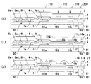
図19(A)、(B)はいずれも、本発明の実施の形態6の電気光学装置の画素の一部を切断したときの断面図である。なお、本形態の電気光学装置の基本的な構成は、実施の形態1と同様であるため、共通する機能を有する部分には、同一の符号を付して図示することにしてそれらの詳細な説明を省略する。
【0114】
実施の形態1ないし5では、高低差解消膜として導電膜を形成した例であったが、本形態では、図19(A)に示すように、高低差解消膜として絶縁膜を利用している。
【0115】
すなわち、本形態でも、実施の形態1と同様、光反射膜8aの表面には、凸部8bおよび凹部8cを備えた凹凸パターン8gが形成され、かつ、走査線3aと同層の容量線3b並びにゲート電極、TFT30を構成する半導体膜1a、その延設部分1f、データ線6aと同層のドレン電極6bが選択的に形成されている。このため、これらの導電膜の形成層数に差があると、光反射膜8aの下層側では、導電膜の膜数や膜厚に相当する高低差が形成される。しかるに本形態では、導電膜の形成層数が少ない領域、すなわち、第3領域10cには、下地絶縁膜11と同層の高低差解消膜11fが形成されている一方、第3領域10cより導電膜の形成層数が多い第2領域10bには、下地保護膜11と同層の絶縁膜が形成されていない。従って、第2領域10bと第3領域10cとでは、高低差解消膜11fによって、凹凸形成層13aの下層側の高低差が解消されている。
【0116】
それ故、感光性樹脂13に対する露光を行って凹凸形成層13aを形成する際、第1領域10a、第2領域10b、および第3領域10cのいずれの領域においても、感光性樹脂13に対して露光ムラが発生しないので、所望の凹凸形成層13aを形成できるなど、実施の形態1と略同様な効果を奏する。
【0117】
その他の構成は、実施の形態1と同様であるため、共通する部分には同一の符号を付して図示することにして、それらの説明を省略する。
【0118】
なお、図19(A)には、高低差解消膜11fとして、下地保護膜11と同層の絶縁膜を利用した例を示してあるが、図19(B)に示すように、下地保護膜11を形成しない場合にも、高低差解消膜11fとしての絶縁膜を形成してもよい。また、絶縁膜からなる高低差解消膜を形成するにあたっては、例えば、層間絶縁膜4を選択的に形成してもよい。
【0119】
[実施の形態7]
図20は、本発明の実施の形態7の電気光学装置の画素の一部を切断したときの断面図である。なお、本形態の電気光学装置の基本的な構成は、実施の形態1と同様であるため、共通する機能を有する部分には、同一の符号を付して図示することにしてそれらの詳細な説明を省略する。
【0120】
図20に示すように、本形態では、光反射膜8aの表面に、凸部8bおよび凹部8cを備えた凹凸パターン8gを構成するにあたって、感光性樹脂13を完全露光して凹凸形成層13aを所定パターンで選択的に残し、凹凸形成層13aの有無によって光反射膜8aの表面に凹凸パターン8gを付与してもよい。このような場合には、凹凸形成層13aにエッジが発生するので、凹凸形成層13aの上層にもう1層、流動性の高い感光性樹脂層からなる上層絶縁膜7aを塗布、形成した後、その上層側に光反射膜8aを形成する.
このような形態においても本発明を適用してもよい。すなわち、図示および説明を省略するが、凹凸形成層13aの下層側に高低差があると、露光ムラが発生するので、実施の形態1ないし5で説明した高低差解消膜を形成する。
【0121】
[実施の形態8]
図21は、本発明の実施の形態8の電気光学装置の画素の一部を切断したときの断面図である。なお、本形態の電気光学装置の基本的な構成は、実施の形態1と同様であるため、共通する機能を有する部分には、同一の符号を付して図示することにしてそれらの詳細な説明を省略する。
【0122】
実施の形態1ないし7では、画素の略全域に光反射膜8aを形成した全反射型の電気光学装置100の例であったが、図21に示すように、光反射膜8aに光透過窓8dを形成し、かつ、凹凸形成層13aについては、光透過窓8dを避けるように形成すれば、半透過・反射型の電気光学装置100を構成することができる。すなわち、光透過窓8dに相当する部分には、ITO膜からなる画素電極9aは存在するが、光反射膜8aが存在しないので、TFTアレイ基板10の側にバックライト装置(図示せず)を配置し、このバックライト装置から出射された光をTFTアレイ基板10の側から入射させれば、光反射膜8aが形成されていない光透過窓8dに向かう光は、光透過窓8dを介して対向基板20側に透過し、表示に寄与する(透過モード)。
【0123】
このような形態においても本発明を適用してもよい。すなわち、図示および説明を省略するが、凹凸形成層13aの下層側に高低差があると、露光ムラが発生するので、実施の形態1ないし5で説明した高低差解消膜を形成する。ただし、先にも説明したように、光透過窓の領域には、高低差解消膜を形成しないほうが望ましい。
【0124】
[その他の実施の形態]
上記形態では、画素電極9aを光反射膜8aの上層側に積層したが、液晶50の分極配向が問題とならない場合には、画素電極9aを光反射膜8aの下層側に積層してもよい。
【0125】
また、全反射型の電気光学装置100の場合には、画素電極9aを形成せずに、光反射膜8aのみを画素電極として用いてもよい。
【0126】
さらに、上記形態では、画素スイッチング用のアクティブ素子としてTFTを用いた例を説明したが、アクティブ素子としてMIM(Metal Insulator Metal)素子などの薄膜ダイオード素子(TFD素子/Thin
Film Diode素子)を用いた場合も同様である。
【0127】
[電気光学装置の電子機器への適用]
このように構成した半透過・反射型の電気光学装置100は、各種の電子機器の表示部として用いることができるが、その一例を、図22、図23、および図24を参照して説明する。
【0128】
図22は、本発明に係る電気光学装置を表示装置として用いた電子機器の回路構成を示すブロック図である。
【0129】
図22において、電子機器は、表示情報出力源70、表示情報処理回路71、電源回路72、タイミングジェネレータ73、そして液晶装置74を有する。また、液晶装置74は、液晶表示パネル75および駆動回路76を有する。液晶装置74としては、前述した電気光学装置100を用いることができる。
【0130】
表示情報出力源70は、ROM(Read Only Memory)、RAM(Random Access Memory)等といったメモリ、各種ディスク等といったストレージユニット、デジタル画像信号を同調出力する同調回路等を備え、タイミングジェネレータ73によって生成された各種のクロック信号に基づいて、所定フォーマットの画像信号等といった表示情報を表示情報処理回路71に供給する。
【0131】
表示情報処理回路71は、シリアル−パラレル変換回路や、増幅・反転回路、ローテーション回路、ガンマ補正回路、クランプ回路等といった周知の各種回路を備え、入力した表示情報の処理を実行して、その画像信号をクロック信号CLKと共に駆動回路76へ供給する。電源回路72は、各構成要素に所定の電圧を供給する。
【0132】
図23は、本発明に係る電子機器の一実施形態であるモバイル型のパーソナルコンピュータを示している。ここに示すパーソナルコンピュータ80は、キーボード81を備えた本体部82と、液晶表示ユニット83とを有する。液晶表示ユニット83は、前述した電気光学装置100を含んで構成される。
【0133】
図24は、本発明に係る電子機器の他の実施形態である携帯電話機を示している。ここに示す携帯電話機90は、複数の操作ボタン91と、前述した電気光学装置100からなる表示部とを有している。
【0134】
【発明の効果】
以上説明したとおり、本発明に係る反射型電気光学装置において、反射型の電気光学装置において、各種配線やアクティブ素子を構成する導電膜の形成層数に差があると、その膜厚に相当する高低差、段差が形成されるが、本発明では、導電膜の形成層数が少ない領域に高低差解消膜が形成されており、この高低差解消膜によって、凹凸形成層の下層側では高低差、段差が解消されている。従って、感光性樹脂に対する露光を行って凹凸形成層を形成する際、高所部分と低所部分との間に顕著な高低差がないため、露光ムラが発生しない。また、高低差がある領域に感光性樹脂を塗布すると、高い領域には感光性樹脂が薄く形成される一方、低い領域には感光性樹脂が厚く形成されるため、露光および現像の後、感光性樹脂を加熱、溶融させて、なだらかな凹凸を表面に備えた凹凸形成層を形成する際、高い領域では感光性樹脂が薄いため、樹脂の垂れが小さいので、比較的大きな凹凸が形成される傾向にあるが、本発明では、このような問題も解消することができる。それ故、凹凸形成層を目論見どおりに形成できるので、光反射膜の表面に所望の凹凸パターンを形成することができる。また、高低差解消膜は、配線を構成する導電膜、アクティブ素子を構成する導電膜、あるいは絶縁膜から形成されているため、高低差解消膜を形成するにあたって製造工程を追加する必要がない。さらに、画素電極の下層側に高低差があると液晶などの電気光学物質層の層厚が領域毎に異なることになるが、本発明では、高低差が解消されているので、表示品位が向上するという利点もある。
【図面の簡単な説明】
【図1】 本発明に係る電気光学装置を対向基板の側からみたときの平面図である。
【図2】 図1のH−H′線における断面図である。
【図3】 電気光学装置において、マトリクス状に配置された複数の画素に形成された各種素子、配線などの等価回路図である。
【図4】 本発明の実施の形態1に係るTFTアレイ基板の画素構成を示す平面図である。
【図5】 図4に示すTFTアレイ基板の画素群から配線、およびTFTを構成する導電膜のみを抜き出して示す平面図である。
【図6】 図4のA−A′線に相当する位置での電気光学装置の断面図である。
【図7】 (A)〜(C)は、図5に示すTFTアレイ基板の製造方法を示す工程断面図である。
【図8】 (D)〜(G)は、図5に示すTFTアレイ基板の製造方法を示す工程断面図である。
【図9】 (H)〜(J)は、図5に示すTFTアレイ基板の製造方法を示す工程断面図である。
【図10】 (K)、(L)は、図5に示すTFTアレイ基板の製造方法を示す工程断面図である。
【図11】 本発明の実施の形態2に係るTFTアレイ基板の画素構成を示す平面図である。
【図12】 図11のB−B′線に相当する位置での電気光学装置の断面図である。
【図13】 本発明の実施の形態3に係るTFTアレイ基板の画素構成を示す平面図である。
【図14】 図13のC−C′線に相当する位置での電気光学装置の断面図である。
【図15】 本発明の実施の形態4に係るTFTアレイ基板の画素構成を示す平面図である。
【図16】 図15のD−D′線に相当する位置での電気光学装置の断面図である。
【図17】 本発明の実施の形態5に係るTFTアレイ基板の画素構成を示す平面図である。
【図18】 図17のE−E′線に相当する位置での電気光学装置の断面図である。
【図19】 (A)、(B)はいずれも、本発明の実施の形態6に係る電気光学装置の断面図である。
【図20】 本発明の実施の形態7に係る電気光学装置の断面図である。
【図21】 本発明の実施の形態8に係る電気光学装置の断面図である。
【図22】 本発明に係る電気光学装置を表示装置として用いた電子機器の回路構成を示すブロック図である。
【図23】 本発明に係る電気光学装置を用いた電子機器の一実施形態としてのモバイル型のパーソナルコンピュータを示す説明図である。
【図24】 本発明に係る電気光学装置を用いた電子機器の一実施形態としての携帯電話機の説明図である。
【図25】 従来のTFTアレイ基板の画素構成を示す平面図である。
【図26】 図25のG−G′線に相当する位置での電気光学装置の断面図である。
【図27】 従来のTFTアレイ基板に凹凸形成層を形成するための感光性樹脂に対する露光工程の説明図である。
【符号の説明】
1a 半導体膜、2 ゲート絶縁膜、3a 走査線、3b 容量線、3f、6f高低差解消膜、4 層間絶縁膜、6a データ線、6b ドレイン電極、8a光反射膜、8b 凹凸パターンの凸部、8c 凹凸パターンの凹部、8d 光透過窓、8g 光反射膜表面の凹凸パターン、9a 画素電極、10 TFTアレイ基板、11 下地保護膜、11f 高低差解消膜、13 感光性樹脂、13a 凹凸形成層、20 対向基板、21 対向電極、30 画素スイッチング用のTFT、50 液晶、60 蓄積容量、100 電気光学装置、100a 画素[0001]
BACKGROUND OF THE INVENTION
The present invention relates to a reflective electro-optical device and an electronic apparatus using the same. More specifically, the present invention relates to a pixel configuration of a reflection type electro-optical device.
[0002]
[Prior art]
Electro-optical devices such as liquid crystal devices are used as direct-view display devices for various devices. Among such electro-optical devices, for example, in an active matrix liquid crystal device using a TFT as a non-linear element for pixel switching, as shown in FIGS. 25 and 26, a
[0003]
In the case of a reflective type liquid crystal device, a
[0004]
However, in the reflection type liquid crystal device, when the directionality of the light reflected by the
[0005]
In the example shown here, as shown in FIG. 27, the
[0006]
That is, when the
[0007]
[Problems to be solved by the invention]
However, in the conventional liquid crystal device, various wirings and conductive films constituting the
[0008]
Further, when the
[0009]
When such exposure unevenness occurs, the concave / convex forming
[0010]
In some cases, the concavo-convex forming
[0011]
In addition, when a photosensitive resin is applied to an area having a height difference, as shown in FIG. 27, the photosensitive resin is thinly formed in the high area by the flattening action, while the photosensitive resin is thickly formed in the low area. Is done. For this reason, after exposure and development, when the
[0012]
In view of the above problems, the object of the present invention is to make the unevenness shape uneven when forming an unevenness formation layer using photolithography technology by making the state of the lower layer side of the unevenness formation layer uniform. It is an object of the present invention to provide a reflection type electro-optical device and an electronic apparatus that do not generate any problem. In addition, it is an object of the present invention to provide a reflection type electro-optical device and an electronic apparatus that can improve the cell gap uniformity of the reflection part and improve the display quality such as contrast by eliminating the step in the reflection region.
[0013]
[Means for Solving the Problems]
In order to solve the above-described problems, in the present invention, at least a pixel switching active element that is electrically connected to one or a plurality of wirings for each pixel and a light reflection layer are provided on a substrate that sandwiches an electro-optic material. Reflection in which a concavo-convex forming layer for providing a predetermined concavo-convex pattern on the surface of the light reflection film is formed in a region overlapping the light reflection film on a lower layer side of the light reflection film. In the type electro-optical device, the active element is formed in a region where the conductive film constituting the active element is not disposed in a region overlapping the projection-depression formation layer on the lower layer side of the projection-depression formation layer. An elevation difference eliminating film for eliminating the elevation difference formed by the presence or absence of the conductive film is formed. The elevation difference elimination film includes the conductive film constituting the wiring, the conductive film constituting the active element, and the insulating film. Characterized by comprising formed from at least one layer of the film.
[0014]
In a reflection type electro-optical device, if there is a difference in the number of conductive films forming various wirings and active elements, a difference in height and a step corresponding to the film thickness are formed. An elevation difference eliminating film is formed in a region where the number of formation layers is small, and the elevation difference eliminating film eliminates the elevation difference and the elevation difference on the lower layer side of the unevenness forming layer. Accordingly, when the unevenness forming layer is formed by exposing the photosensitive resin, there is no significant difference in height between the high portion and the low portion, so that no exposure unevenness occurs. In addition, when a photosensitive resin is applied to an area with a difference in height, a thin photosensitive resin is formed in a high area, while a thick photosensitive resin is formed in a low area. When a concavo-convex forming layer having gentle unevenness on the surface is formed by heating and melting the photosensitive resin, since the photosensitive resin is thin in the high region, the dripping of the resin is small, so that relatively large unevenness is formed. Although there is a tendency, in the present invention, such a problem can be solved. Therefore, since the unevenness forming layer can be formed as intended, a desired uneven pattern can be formed on the surface of the light reflecting film. In addition, since the height difference eliminating film is formed of a conductive film that constitutes a wiring, a conductive film that constitutes an active element, or an insulating film, it is not necessary to add a manufacturing process in forming the elevation difference eliminating film. Furthermore, if there is a height difference on the lower layer side of the pixel electrode, the layer thickness of the electro-optic material layer such as a liquid crystal will differ from region to region. However, in the present invention, since the height difference is eliminated, display quality is improved. There is also an advantage of doing.
[0015]
In the present invention, it is preferable that the height difference eliminating film is formed from at least one of a conductive film constituting the wiring, a conductive film constituting the active element, and an insulating film. With this configuration, there are a region where the conductive film exists and a region where the conductive film does not exist, and exposure unevenness tends to occur due to the presence or absence of light reflected from the conductive film and variations in intensity during exposure. In the present invention, since the conductive film is formed over substantially the entire pixel, uneven exposure does not occur. In addition, there is a difference in heat transfer between the region where the conductive film exists and the region where the conductive film does not exist, and temperature variations are likely to occur. However, if the conductive film is formed almost entirely, the temperature variations are reduced. Therefore, the curing rate of the photosensitive resin can be made uniform. Therefore, since the unevenness forming layer can be formed as intended, a desired uneven pattern can be formed on the surface of the light reflecting film. Further, since the height difference eliminating film is formed in the same layer as the conductive film constituting the wiring or active element, it is not necessary to add a manufacturing process when forming the height difference eliminating film.
[0016]
In the present invention, the height difference eliminating film is eliminated by selectively forming, for example, a region where the number of conductive film layers forming the active element is small.
[0017]
In the present invention, when the active element is a thin film transistor connected to a scanning line and a data line as the wiring, for example, a conductive film formed simultaneously in the same layer as the scanning line as the height difference eliminating film, Alternatively, at least one of the conductive films formed simultaneously in the same layer as the data line is formed.
[0018]
Further, in the present invention, when the active element is a thin film transistor connected to a scanning line and a data line as the wiring, and the pixel has a capacitor line for forming a storage capacitor, As the height difference elimination film, for example, at least one of a conductive film in the same layer as the scanning line, a conductive film in the same layer as the capacitor line, or a conductive film in the same layer as the data line is formed.
[0019]
In the present invention, it is preferable that the height difference eliminating film is formed in an island shape by being separated from the wiring or the conductive film constituting the active element. With this configuration, it is possible to prevent the occurrence of parasitic capacitance in a region where the other layer and the height difference eliminating film overlap in a plane.
[0020]
In the present invention, the height difference eliminating film may be extended from the wiring or the conductive film constituting the active element. For example, the height difference eliminating film may be formed by extending the upper electrode of the capacitor portion.
[0021]
Furthermore, in another embodiment of the present invention, on the substrate sandwiching the electro-optic material, at least an active element for pixel switching electrically connected to one or a plurality of wirings for each pixel, a light reflection film, and A reflective electro-optical device in which a concavo-convex forming layer for providing a predetermined concavo-convex pattern on the surface of the light reflecting film is formed in a region overlapping with the light reflecting film on a lower layer side of the light reflecting film In the region where the conductive layer constituting the active element is not arranged in the region overlapping the planar surface of the concave / convex forming layer on the lower layer side of the concave / convex forming layer, the region is electrically insulated from other regions. An island pattern is formed, and the island pattern is formed from at least one of a conductive film forming the wiring and a conductive film forming the active element.
[0022]
In the present invention, the concavo-convex forming layer may be made of a photosensitive resin having concavo-convex corresponding to a gentle change in film thickness on the surface. In this case, the concavo-convex formation is formed on the surface of the light reflecting film. The uneven pattern is formed by reflecting the unevenness formed on the surface of the layer. Such a form can be realized by forming the concavo-convex forming layer by half exposure through an exposure mask for the photosensitive resin and development.
[0023]
In the present invention, the concavo-convex forming layer may be made of a photosensitive resin selectively formed in a predetermined pattern. In this case, the surface of the light reflecting film is provided with the presence or absence of the concavo-convex forming layer. Correspondingly, the uneven pattern is formed. Such a form can be realized by forming the concavo-convex forming layer by exposure through an exposure mask to the photosensitive resin and development.
[0024]
Here, when the unevenness forming layer has an edge, an upper insulating film is formed on the unevenness forming layer. If comprised in this way, the unevenness | corrugation which the said unevenness | corrugation formation layer will reflect in the surface of the said light reflection film through the said upper-layer insulating film will form the said unevenness | corrugation pattern.
[0025]
In the present invention, when the electro-optical device is configured as a total reflection type, the unevenness forming layer is formed over substantially the entire area of the pixel.
[0026]
On the other hand, when the electro-optical device according to the present invention is configured as a transflective type, a configuration in which a light transmission window is formed in the light reflection film may be used. In this case, it is desirable not to form the elevation difference eliminating film or the island pattern in the region of the light transmission window in order to prevent a decrease in light transmittance. With this configuration, even if there is uneven exposure in the light transmission window region, it is not necessary to form a concavo-convex shape with a photosensitive resin in this region, so no problem occurs.
[0027]
In the present invention, the electro-optical material is, for example, a liquid crystal.
[0028]
The electro-optical device to which the present invention is applied can be used as a display device of an electronic apparatus such as a mobile computer or a mobile phone.
[0029]
DETAILED DESCRIPTION OF THE INVENTION
Embodiments of the present invention will be described with reference to the drawings.
[0030]
[Embodiment 1]
(Basic configuration of reflective electro-optical device)
FIG. 1 is a plan view of an electro-optical device to which the present invention is applied as viewed from the counter substrate side together with each component, and FIG. 2 is a cross-sectional view taken along line HH ′ of FIG. FIG. 3 is an equivalent circuit diagram of various elements and wirings in a plurality of pixels formed in a matrix in the image display region of the electro-optical device. Note that, in each drawing used in the description of the present embodiment, each layer and each member have different scales so that each layer and each member can be recognized on the drawing.
[0031]
1 and 2, the reflective electro-
[0032]
Instead of forming the data line driving
[0033]
In the
[0034]
Here, the
[0035]
In order to prevent the retained pixel signals S1, S2,... Sn from leaking, a
[0036]
(Configuration of TFT array substrate)
FIG. 4 is a plan view of a plurality of pixel groups adjacent to each other on the TFT array substrate used in the electro-optical device of this embodiment. FIG. 5 is a plan view showing only wirings such as scanning lines, data lines, capacitor lines, and conductive films constituting the
[0037]
4 and 5,
[0038]
As shown in FIG. 6, the cross section taken along the line AA ′ of the pixel region configured in this way is formed on the surface of the
[0039]
An interlayer insulating
[0040]
On the surface of the surface
[0041]
A
[0042]
Here, the
[0043]
An
[0044]
Note that the
[0045]
The
[0046]
In this embodiment, a single gate structure is employed in which only one gate electrode (scanning
[0047]
(Detailed configuration of uneven pattern)
As shown in FIG. 6, in the
[0048]
In constructing such a concavo-
[0049]
Here, the concavo-convex forming
[0050]
As will be described later, such a concavo-convex forming
[0051]
Here, in the
[0052]
(Configuration of counter substrate)
In the
[0053]
(Operation and effect of this form)
In the semi-transmissive / reflective electro-
[0054]
Here, in the
[0055]
Further, when the
[0056]
In addition, when there are a region where a conductive film exists and a region where a conductive film does not exist, exposure unevenness occurs depending on the presence or intensity of light reflected from the conductive film and the intensity of light reflected from the conductive film. Since the conductive film is formed over the entire surface, exposure unevenness does not occur even from this point. In addition, there is a difference in heat transfer between the region where the conductive film exists and the region where the conductive film does not exist, and temperature variations are likely to occur. However, if the conductive film is formed almost entirely, the temperature variations are reduced. Therefore, the curing speed of the
[0057]
Therefore, according to the present embodiment, since the
[0058]
In addition, if there is a difference in height on the lower layer side of the
[0059]
In this embodiment, even if the elevation
[0060]
Furthermore, in the present embodiment, the
[0061]
Furthermore, in this embodiment, the
[0062]
(TFT manufacturing method)
Of the manufacturing processes of the electro-
[0063]
First, as shown in FIG. 7A, after preparing a substrate 10 'made of glass or the like cleaned by ultrasonic cleaning or the like, the substrate temperature is 150 ° C. to 450 ° C. under the plasma CVD method, A base
[0064]
Next, an island-shaped
[0065]
Next, as shown in FIG. 7B, a
[0066]
Next, although not shown, impurity ions are implanted into the
[0067]
Next, as shown in FIG. 7C, the
[0068]
At this time, in this embodiment, the height
[0069]
Next, on the side of the pixel TFT portion and the N-channel TFT portion (not shown) of the drive circuit, about 0.1 × 10 6 using the
[0070]
Next, as shown in FIG. 8D, a resist
[0071]
In place of these impurity introduction steps, high concentration impurities (phosphorus ions) are implanted in a state where a resist mask wider than the gate electrode is formed without implanting low concentration impurities, and the source and drain regions of the offset structure May be formed. Needless to say, a high concentration impurity may be implanted using the
[0072]
Although not shown, the N-channel TFT portion of the peripheral drive circuit portion is formed by such a process. Further, when forming the P-channel TFT portion of the peripheral drive circuit, the pixel portion and the N-channel TFT portion are covered and protected with a resist, and the gate electrode is used as a mask to provide about 0.1 × 10 15 / Cm 2 ~ About 10 × 10 15 / Cm 2 By implanting boron ions at a dose of P, source / drain regions of the P channel are formed in a self-aligned manner. At this time, similarly to the formation of the N-channel TFT portion, about 0.1 × 10 10 using the gate electrode as a mask. 13 / Cm 2 ~ About 10 × 10 13 / Cm 2 After introducing a low concentration impurity (boron ions) at a dose of a low concentration region in the polysilicon film, a mask wider than the gate electrode is formed to reduce the high concentration impurities (boron ions). 0.1 × 10 15 / Cm 2 ~ About 10 × 10 15 / Cm 2 The source region and the drain region of the LDD structure (lightly doped drain structure) may be formed by implanting at a dose of. Alternatively, a source region and a drain region having an offset structure may be formed by implanting high concentration impurities (phosphorus ions) in a state where a mask wider than the gate electrode is formed without implanting low concentration impurities. By these ion implantation processes, CMOS can be realized, and the peripheral drive circuit can be built in the same substrate.
[0073]
Next, as shown in FIG. 8E, after an
[0074]
Next, as shown in FIG. 8F, the
[0075]
When the steps up to here are advanced, the surface of the
[0076]
Next, as shown in FIG. 8G, a surface
[0077]
Next, as shown in FIG. 9H, a positive type
[0078]
Next, as shown in FIG. 9 (I), the
[0079]
During such exposure, the
[0080]
After developing the
[0081]
Note that a
[0082]
Next, as shown in FIG. 10K, a
[0083]
In the thus formed
[0084]
Next, as shown in FIG. 10L, a
[0085]
Thereafter, as shown in FIG. 5, a polyimide film (alignment film 12) is formed on the surface side of the
[0086]
[Embodiment 2]
FIG. 11 is a plan view of a plurality of pixel groups adjacent to each other on the TFT array substrate used in the electro-optical device according to the second embodiment. In this figure, the characteristic portions of this embodiment are indicated by bold lines. FIG. 12 is a cross-sectional view of a part of the pixel of the electro-optical device cut at a position corresponding to the line BB ′ in FIG. The basic configuration of the electro-optical device according to the present embodiment is the same as that of the first embodiment. Therefore, parts having common functions are denoted by the same reference numerals and illustrated in detail. Description is omitted.
[0087]
As shown in FIGS. 11 and 12, also in the
[0088]
Also in this embodiment, in the
[0089]
In addition, in this embodiment, since the
[0090]
In addition, when there are a region where the conductive film exists and a region where the conductive film does not exist, exposure unevenness occurs depending on the presence or intensity of light reflected from the conductive film and the intensity of light reflected from the conductive film. Since the conductive film is formed over substantially the entire surface, exposure unevenness does not occur even from this point.
[0091]
Therefore, according to this embodiment, when half-exposure is performed on the
[0092]
In the present embodiment, even if the elevation
[0093]
[Embodiment 3]
FIG. 13 is a plan view of a plurality of pixel groups adjacent to each other on the TFT array substrate used in the electro-optical device according to the third embodiment. In this figure, the characteristic portions of this embodiment are indicated by bold lines. FIG. 14 is a cross-sectional view of a part of the pixel of the electro-optical device cut at a position corresponding to the line CC ′ in FIG. The basic configuration of the electro-optical device according to the present embodiment is the same as that of the first embodiment. Therefore, parts having common functions are denoted by the same reference numerals and illustrated in detail. Description is omitted.
[0094]
As shown in FIGS. 13 and 14, also in the
[0095]
Also in this embodiment, in the
[0096]
In addition, when there are a region where the conductive film exists and a region where the conductive film does not exist, exposure unevenness occurs depending on the presence or intensity of light reflected from the conductive film and the intensity of light reflected from the conductive film. Since the conductive film is formed over substantially the entire surface, exposure unevenness does not occur even from this point.
[0097]
Therefore, according to this embodiment, when half-exposure is performed on the
[0098]
In this embodiment, even if the height
[0099]
[Embodiment 4]
FIG. 15 is a plan view of a plurality of pixel groups adjacent to each other in the TFT array substrate used in the electro-optical device of the fourth embodiment. In this figure, the characteristic portions of this embodiment are indicated by bold lines. 16 is a cross-sectional view of a part of the pixel of the electro-optical device cut at a position corresponding to the line DD ′ in FIG. The basic configuration of the electro-optical device according to the present embodiment is the same as that of the first embodiment. Therefore, parts having common functions are denoted by the same reference numerals and illustrated in detail. Description is omitted.
[0100]
As shown in FIGS. 13 and 14, also in the
[0101]
Also in this embodiment, a concavo-
[0102]
In the
[0103]
In addition, when there are a region where a conductive film exists and a region where a conductive film does not exist, exposure unevenness occurs depending on the presence or intensity of light reflected from the conductive film and the intensity of light reflected from the conductive film. Since the conductive film is formed over the entire surface, exposure unevenness does not occur even from this point.
[0104]
Therefore, according to this embodiment, when half-exposure is performed on the
[0105]
In the present embodiment, even if the elevation
[0106]
[Embodiment 5]
FIG. 17 is a plan view of a plurality of pixel groups adjacent to each other on the TFT array substrate used in the electro-optical device of the fifth embodiment. In this figure, the characteristic portions of this embodiment are indicated by bold lines. 18 is a cross-sectional view of a part of the pixel of the electro-optical device cut at a position corresponding to the line EE ′ of FIG. The basic configuration of the electro-optical device according to the present embodiment is the same as that of the first embodiment. Therefore, parts having common functions are denoted by the same reference numerals and illustrated in detail. Description is omitted.
[0107]
As shown in FIGS. 17 and 18, also in the
[0108]
Also in this embodiment, a concavo-
[0109]
In the
[0110]
In addition, when there are a region where a conductive film exists and a region where a conductive film does not exist, exposure unevenness occurs depending on the presence or intensity of light reflected from the conductive film and the intensity of light reflected from the conductive film. Since the conductive film is formed over the entire surface, exposure unevenness does not occur even from this point.
[0111]
Therefore, according to this embodiment, when half-exposure is performed on the
[0112]
In this embodiment, even if the height
[0113]
[Embodiment 6]
FIGS. 19A and 19B are cross-sectional views when a part of the pixels of the electro-optical device according to Embodiment 6 of the present invention is cut. The basic configuration of the electro-optical device according to the present embodiment is the same as that of the first embodiment. Therefore, parts having common functions are denoted by the same reference numerals and illustrated in detail. Description is omitted.
[0114]
In the first to fifth embodiments, the conductive film is formed as the height difference eliminating film. However, in this embodiment, as shown in FIG. 19A, an insulating film is used as the height difference eliminating film. .
[0115]
That is, also in the present embodiment, as in the first embodiment, the concave /
[0116]
Therefore, when the concavo-convex forming
[0117]
Since other configurations are the same as those of the first embodiment, common portions are denoted by the same reference numerals, and description thereof is omitted.
[0118]
FIG. 19A shows an example in which an insulating film in the same layer as the base
[0119]
[Embodiment 7]
FIG. 20 is a cross-sectional view of a part of the pixels of the electro-optical device according to the seventh embodiment of the present invention. The basic configuration of the electro-optical device according to the present embodiment is the same as that of the first embodiment. Therefore, parts having common functions are denoted by the same reference numerals and illustrated in detail. Description is omitted.
[0120]
As shown in FIG. 20, in this embodiment, when forming the concave /
The present invention may be applied to such a form. That is, although illustration and description are omitted, if there is a height difference on the lower layer side of the concavo-
[0121]
[Embodiment 8]
FIG. 21 is a cross-sectional view of a part of the pixel of the electro-optical device according to the eighth embodiment of the present invention. The basic configuration of the electro-optical device according to the present embodiment is the same as that of the first embodiment. Therefore, parts having common functions are denoted by the same reference numerals and illustrated in detail. Description is omitted.
[0122]
In the first to seventh embodiments, the example is the total reflection type electro-
[0123]
The present invention may be applied to such a form. That is, although illustration and description are omitted, if there is a height difference on the lower layer side of the
[0124]
[Other embodiments]
In the above embodiment, the
[0125]
In the case of the total reflection type electro-
[0126]
Furthermore, in the above embodiment, an example in which a TFT is used as an active element for pixel switching has been described. However, a thin film diode element (TFD element / Thin element) such as an MIM (Metal Insulator Metal) element is used as the active element.
The same applies to the case of using a Film Diode element.
[0127]
[Application of electro-optical device to electronic equipment]
The transflective / reflective electro-
[0128]
FIG. 22 is a block diagram illustrating a circuit configuration of an electronic apparatus using the electro-optical device according to the invention as a display device.
[0129]
In FIG. 22, the electronic device includes a display
[0130]
The display
[0131]
The display
[0132]
FIG. 23 shows a mobile personal computer which is an embodiment of the electronic apparatus according to the invention. The
[0133]
FIG. 24 shows a mobile phone which is another embodiment of the electronic apparatus according to the invention. A
[0134]
【The invention's effect】
As described above, in the reflective electro-optical device according to the present invention, in the reflective electro-optical device, if there is a difference in the number of conductive layers forming various wirings and active elements, this corresponds to the film thickness. In the present invention, a height difference eliminating film is formed in a region where the number of conductive film formation layers is small, and this height difference eliminating film causes a difference in height on the lower layer side of the unevenness forming layer. , The step has been eliminated. Accordingly, when the unevenness forming layer is formed by exposing the photosensitive resin, there is no significant difference in height between the high portion and the low portion, so that no exposure unevenness occurs. In addition, when a photosensitive resin is applied to an area with a difference in height, a thin photosensitive resin is formed in a high area, while a thick photosensitive resin is formed in a low area. When a concavo-convex forming layer having gentle unevenness on the surface is formed by heating and melting the photosensitive resin, since the photosensitive resin is thin in the high region, the dripping of the resin is small, so that relatively large unevenness is formed. Although there is a tendency, in the present invention, such a problem can be solved. Therefore, since the unevenness forming layer can be formed as intended, a desired uneven pattern can be formed on the surface of the light reflecting film. In addition, since the height difference eliminating film is formed of a conductive film that constitutes a wiring, a conductive film that constitutes an active element, or an insulating film, it is not necessary to add a manufacturing process in forming the elevation difference eliminating film. Furthermore, if there is a height difference on the lower layer side of the pixel electrode, the layer thickness of the electro-optic material layer such as a liquid crystal will differ from region to region. However, in the present invention, since the height difference is eliminated, display quality is improved. There is also an advantage of doing.
[Brief description of the drawings]
FIG. 1 is a plan view of an electro-optical device according to the present invention as viewed from a counter substrate side.
FIG. 2 is a cross-sectional view taken along the line HH ′ of FIG.
FIG. 3 is an equivalent circuit diagram of various elements and wirings formed in a plurality of pixels arranged in a matrix in the electro-optical device.
FIG. 4 is a plan view showing a pixel configuration of the TFT array substrate according to the first embodiment of the present invention.
5 is a plan view showing a wiring and only a conductive film constituting the TFT extracted from the pixel group of the TFT array substrate shown in FIG. 4;
6 is a cross-sectional view of the electro-optical device at a position corresponding to the line AA ′ in FIG. 4;
7A to 7C are process cross-sectional views illustrating a method of manufacturing the TFT array substrate shown in FIG.
8D to 8G are process cross-sectional views illustrating a method for manufacturing the TFT array substrate shown in FIG.
FIGS. 9H to 9J are process cross-sectional views illustrating a method of manufacturing the TFT array substrate shown in FIG.
FIGS. 10K and 10L are process cross-sectional views illustrating a method of manufacturing the TFT array substrate shown in FIG.
FIG. 11 is a plan view showing a pixel configuration of a TFT array substrate according to a second embodiment of the present invention.
12 is a cross-sectional view of the electro-optical device at a position corresponding to the line BB ′ in FIG.
FIG. 13 is a plan view showing a pixel configuration of a TFT array substrate according to a third embodiment of the present invention.
14 is a cross-sectional view of the electro-optical device at a position corresponding to the line CC ′ in FIG. 13;
FIG. 15 is a plan view showing a pixel configuration of a TFT array substrate according to a fourth embodiment of the present invention.
16 is a cross-sectional view of the electro-optical device at a position corresponding to the line DD ′ in FIG.
FIG. 17 is a plan view showing a pixel configuration of a TFT array substrate according to a fifth embodiment of the present invention.
18 is a cross-sectional view of the electro-optical device at a position corresponding to the line EE ′ of FIG.
FIGS. 19A and 19B are cross-sectional views of an electro-optical device according to Embodiment 6 of the present invention.
FIG. 20 is a cross-sectional view of an electro-optical device according to a seventh embodiment of the present invention.
FIG. 21 is a sectional view of an electro-optical device according to an eighth embodiment of the present invention.
FIG. 22 is a block diagram illustrating a circuit configuration of an electronic apparatus using the electro-optical device according to the invention as a display device.
FIG. 23 is an explanatory diagram showing a mobile personal computer as an embodiment of an electronic apparatus using the electro-optical device according to the invention.
FIG. 24 is an explanatory diagram of a mobile phone as an embodiment of an electronic apparatus using the electro-optical device according to the invention.
FIG. 25 is a plan view showing a pixel configuration of a conventional TFT array substrate.
26 is a cross-sectional view of the electro-optical device at a position corresponding to the GG ′ line in FIG. 25. FIG.
FIG. 27 is an explanatory diagram of an exposure process for a photosensitive resin for forming a concavo-convex forming layer on a conventional TFT array substrate.
[Explanation of symbols]
1a semiconductor film, 2 gate insulating film, 3a scanning line, 3b capacitance line, 3f, 6f height difference eliminating film, 4 interlayer insulating film, 6a data line, 6b drain electrode, 8a light reflecting film, 8b convex portion of uneven pattern, 8c Concavity and convexity recesses, 8d Light transmission window, 8g Light reflection film surface unevenness pattern, 9a Pixel electrode, 10 TFT array substrate, 11 Base protective film, 11f Height difference elimination film, 13 Photosensitive resin, 13a Concavity and convexity formation layer, 20 counter substrate, 21 counter electrode, 30 pixel switching TFT, 50 liquid crystal, 60 storage capacitor, 100 electro-optical device, 100a pixel
Claims (27)
前記凹凸形成層の下層側で当該凹凸形成層と平面的に重なる領域のうち、前記アクティブ素子を構成する導電膜が配置されていない領域には、前記アクティブ素子を形成する導電膜の有無によって形成される高低差を解消するための高低差解消膜が形成され、
当該高低差解消膜は、前記配線を構成する導電膜、前記アクティブ素子を構成する導電膜、および絶縁膜のうちの少なくとも一層から形成されてなることを特徴とする反射型電気光学装置。On the substrate holding the electro-optic material, at least each pixel is formed with an active element for pixel switching that is electrically connected to one or a plurality of wirings, and a light reflecting film. In a reflective electro-optical device in which a concavo-convex forming layer for providing a predetermined concavo-convex pattern on the surface of the light reflecting film is formed in a region overlapping the light reflecting film on the lower layer side,
Of the region overlapping the concavo-convex forming layer on the lower layer side of the concavo-convex forming layer, the region where the conductive film constituting the active element is not disposed is formed depending on the presence or absence of the conductive film forming the active element. A height difference eliminating film is formed to eliminate the height difference
The reflection type electro-optical device, wherein the height difference eliminating film is formed of at least one of a conductive film constituting the wiring, a conductive film constituting the active element, and an insulating film.
前記高低差解消膜には、前記走査線と同層に同時形成された導電膜、および前記データ線と同層に同時形成された導電膜のうちの少なくとも一方が含まれていることを特徴とする反射型電気光学装置。In Claim 1, the active element is a thin film transistor connected to a scanning line and a data line as the wiring,
The elevation difference elimination film includes at least one of a conductive film formed simultaneously in the same layer as the scanning line and a conductive film formed simultaneously in the same layer as the data line. Reflective electro-optical device.
前記高低差解消膜には、前記走査線と同層に同時形成された導電膜、前記容量線と同層に同時形成された導電膜、および前記データ線と同層に同時形成された導電膜のうちの少なくとも一層が含まれていることを特徴とする反射型電気光学装置。2. The active element according to claim 1, wherein the active element is a thin film transistor connected to a scanning line and a data line as the wiring, and a capacitor line for forming a storage capacitor is formed in the pixel.
The height difference eliminating film includes a conductive film formed simultaneously in the same layer as the scanning line, a conductive film formed simultaneously in the same layer as the capacitor line, and a conductive film formed simultaneously in the same layer as the data line. A reflective electro-optical device characterized in that at least one of them is included.
前記光反射膜の表面には、前記凹凸形成層の表面に形成された凹凸が反映されて前記凹凸パターンが形成されていることを特徴とする反射型電気光学装置。In Claim 1, the concavo-convex forming layer is made of a photosensitive resin provided with concavo-convex corresponding to a gentle film thickness change on the surface,
The reflective electro-optical device is characterized in that the unevenness pattern formed on the surface of the unevenness forming layer is reflected on the surface of the light reflecting film.
前記光反射膜の表面には、前記凹凸形成層の有無に対応して前記凹凸パターンが形成されていることを特徴とする反射型電気光学装置。In Claim 1, the unevenness forming layer is made of a photosensitive resin selectively formed in a predetermined pattern,
The reflection type electro-optical device, wherein the concave / convex pattern is formed on the surface of the light reflecting film corresponding to the presence / absence of the concave / convex forming layer.
前記凹凸形成層の下層側で当該凹凸形成層と平面的に重なる領域のうち、前記アクティブ素子を構成する導電膜が配置されていない領域には、電気的に他の領域から絶縁された島状パターンが形成され、該島状パターンは、前記配線を構成する導電膜、および前記アクティブ素子を構成する導電膜のうちの少なくとも一層から形成されてなることを特徴とする反射型電気光学装置。On the substrate holding the electro-optic material, at least each pixel is formed with an active element for pixel switching that is electrically connected to one or a plurality of wirings, and a light reflecting film. In a reflective electro-optical device in which a concavo-convex forming layer for providing a predetermined concavo-convex pattern on the surface of the light reflecting film is formed in a region overlapping the light reflecting film on the lower layer side,
Of the region overlapping the concavo-convex formation layer on the lower layer side of the concavo-convex formation layer, the region where the conductive film constituting the active element is not disposed is an island shape electrically insulated from other regions A reflective electro-optical device, wherein a pattern is formed, and the island pattern is formed from at least one of a conductive film constituting the wiring and a conductive film constituting the active element.
前記光反射膜の表面には、前記凹凸形成層の表面に形成された凹凸が反映されて前記凹凸パターンが形成されていることを特徴とする反射型電気光学装置。In Claim 16, the concavo-convex forming layer is made of a photosensitive resin provided with concavo-convex corresponding to a gentle film thickness change on the surface,
The reflective electro-optical device is characterized in that the unevenness pattern formed on the surface of the unevenness forming layer is reflected on the surface of the light reflecting film.
前記光反射膜の表面には、前記凹凸形成層の有無に対応して前記凹凸パターンが形成されていることを特徴とする反射型電気光学装置。In Claim 16, said unevenness formation layer consists of photosensitive resin selectively formed in the predetermined pattern,
The reflection type electro-optical device, wherein the concave / convex pattern is formed on the surface of the light reflecting film corresponding to the presence / absence of the concave / convex forming layer.
Priority Applications (6)
| Application Number | Priority Date | Filing Date | Title |
|---|---|---|---|
| JP2002366709A JP3722116B2 (en) | 2002-01-23 | 2002-12-18 | Reflective electro-optical device and electronic apparatus |
| US10/341,517 US6806927B2 (en) | 2002-01-23 | 2003-01-14 | Step-eliminating film and island-shaped pattern composed of conductive film for a reflective electrooptic device and electronic apparatus |
| CNB031007104A CN1231803C (en) | 2002-01-23 | 2003-01-21 | Reflection electrooptical device and electronic equipment |
| KR10-2003-0004199A KR100511578B1 (en) | 2002-01-23 | 2003-01-22 | Reflective type electrooptical device and electronic apparatus |
| TW092101371A TW594160B (en) | 2002-01-23 | 2003-01-22 | Reflective electrooptic device and electronic apparatus |
| CNU032363443U CN2685924Y (en) | 2002-01-23 | 2003-01-22 | Reflective photoelectric apparatus and electronic equipment |
Applications Claiming Priority (3)
| Application Number | Priority Date | Filing Date | Title |
|---|---|---|---|
| JP2002014606 | 2002-01-23 | ||
| JP2002-14606 | 2002-01-23 | ||
| JP2002366709A JP3722116B2 (en) | 2002-01-23 | 2002-12-18 | Reflective electro-optical device and electronic apparatus |
Publications (2)
| Publication Number | Publication Date |
|---|---|
| JP2003287772A JP2003287772A (en) | 2003-10-10 |
| JP3722116B2 true JP3722116B2 (en) | 2005-11-30 |
Family
ID=27667417
Family Applications (1)
| Application Number | Title | Priority Date | Filing Date |
|---|---|---|---|
| JP2002366709A Expired - Lifetime JP3722116B2 (en) | 2002-01-23 | 2002-12-18 | Reflective electro-optical device and electronic apparatus |
Country Status (5)
| Country | Link |
|---|---|
| US (1) | US6806927B2 (en) |
| JP (1) | JP3722116B2 (en) |
| KR (1) | KR100511578B1 (en) |
| CN (2) | CN1231803C (en) |
| TW (1) | TW594160B (en) |
Families Citing this family (11)
| Publication number | Priority date | Publication date | Assignee | Title |
|---|---|---|---|---|
| JP2004061775A (en) * | 2002-07-26 | 2004-02-26 | Alps Electric Co Ltd | Active matrix type display device |
| JP2005159293A (en) | 2003-09-18 | 2005-06-16 | Nec Kagoshima Ltd | Device and method for treating substrate |
| EP1704443B1 (en) * | 2004-01-05 | 2007-06-06 | TPO Hong Kong Holding Limited | Liquid crystal display device having esd protection circuit and method for manufacturing the same |
| KR101064185B1 (en) * | 2004-02-05 | 2011-09-14 | 삼성전자주식회사 | Array substrate and manufacturing method thereof, and liquid crystal display having same |
| JP3901172B2 (en) * | 2004-05-28 | 2007-04-04 | セイコーエプソン株式会社 | Liquid crystal display device and electronic device |
| KR101043675B1 (en) * | 2004-06-05 | 2011-06-22 | 엘지디스플레이 주식회사 | Semi-transmissive thin film transistor substrate and manufacturing method thereof |
| JP4258532B2 (en) * | 2006-06-30 | 2009-04-30 | カシオ計算機株式会社 | Thin film device substrate and manufacturing method thereof |
| KR101433613B1 (en) * | 2007-11-01 | 2014-08-27 | 삼성디스플레이 주식회사 | Method of manufacturing display device and display device therefrom |
| CN107154346B (en) * | 2017-05-19 | 2021-03-16 | 京东方科技集团股份有限公司 | A method for doping a film, a thin film transistor and a method for making the same |
| CN109116647B (en) | 2018-09-17 | 2021-08-27 | 京东方科技集团股份有限公司 | Array substrate, preparation method thereof and display device |
| CN109698206B (en) * | 2018-12-26 | 2021-05-28 | 上海天马微电子有限公司 | Array substrate and preparation method thereof, display panel and display device |
Family Cites Families (7)
| Publication number | Priority date | Publication date | Assignee | Title |
|---|---|---|---|---|
| JPH10221704A (en) | 1997-02-07 | 1998-08-21 | Sharp Corp | Reflection type liquid crystal display device and its manufacture |
| JP3270821B2 (en) * | 1997-03-12 | 2002-04-02 | シャープ株式会社 | Reflective liquid crystal display device and method of manufacturing the same |
| JP2000002872A (en) * | 1998-06-16 | 2000-01-07 | Semiconductor Energy Lab Co Ltd | Liquid crystal display device and its manufacture |
| JP3768367B2 (en) * | 1998-10-14 | 2006-04-19 | シャープ株式会社 | Liquid crystal display |
| JP3487782B2 (en) * | 1999-03-17 | 2004-01-19 | 株式会社日立製作所 | Liquid crystal display |
| JP2001337208A (en) * | 2000-03-23 | 2001-12-07 | Matsushita Electric Ind Co Ltd | Rough body, reflecting plate, reflective liquid crystal display device, method for producing the same and apparatus therefor |
| JP5057613B2 (en) * | 2000-04-27 | 2012-10-24 | 株式会社半導体エネルギー研究所 | Semiconductor device and electronic equipment |
-
2002
- 2002-12-18 JP JP2002366709A patent/JP3722116B2/en not_active Expired - Lifetime
-
2003
- 2003-01-14 US US10/341,517 patent/US6806927B2/en not_active Expired - Lifetime
- 2003-01-21 CN CNB031007104A patent/CN1231803C/en not_active Expired - Lifetime
- 2003-01-22 CN CNU032363443U patent/CN2685924Y/en not_active Expired - Lifetime
- 2003-01-22 TW TW092101371A patent/TW594160B/en not_active IP Right Cessation
- 2003-01-22 KR KR10-2003-0004199A patent/KR100511578B1/en active IP Right Grant
Also Published As
| Publication number | Publication date |
|---|---|
| US20030174267A1 (en) | 2003-09-18 |
| KR20030064300A (en) | 2003-07-31 |
| TW200302939A (en) | 2003-08-16 |
| CN1231803C (en) | 2005-12-14 |
| CN1434337A (en) | 2003-08-06 |
| TW594160B (en) | 2004-06-21 |
| JP2003287772A (en) | 2003-10-10 |
| KR100511578B1 (en) | 2005-09-02 |
| CN2685924Y (en) | 2005-03-16 |
| US6806927B2 (en) | 2004-10-19 |
Similar Documents
| Publication | Publication Date | Title |
|---|---|---|
| JP3714244B2 (en) | Transflective / reflective electro-optical device manufacturing method, transflective / reflective electro-optical device, and electronic apparatus | |
| JP3675427B2 (en) | Transflective liquid crystal device and electronic equipment using the same | |
| JP3722116B2 (en) | Reflective electro-optical device and electronic apparatus | |
| KR100514507B1 (en) | Electrooptic device and production method therefor | |
| JP4154880B2 (en) | Electro-optical device and manufacturing method thereof | |
| JP4035992B2 (en) | Electro-optical device, electronic apparatus, and method of manufacturing electro-optical device | |
| JP3951694B2 (en) | Transflective / reflective electro-optical device, electronic apparatus, and method of manufacturing transflective / reflective electro-optical device | |
| JP3747828B2 (en) | Electro-optical device and manufacturing method thereof | |
| JP3979077B2 (en) | Electro-optical device and electronic apparatus | |
| JP4400027B2 (en) | Transflective / reflective electro-optical device and electronic apparatus using the same | |
| JP2003029275A (en) | Electro-optical device, electronic apparatus, and method of manufacturing electro-optical device | |
| JP2003195285A (en) | Reflective electro-optical device, electronic apparatus, and method of manufacturing reflective electro-optical device | |
| JP4023111B2 (en) | Manufacturing method of electro-optical device | |
| JP2003029298A (en) | Thin-film semiconductor device, electro-optical device, electronic equipment, thin-film semiconductor device, and method of manufacturing electro-optical device | |
| JP2005275432A (en) | Electro-optical device and electronic apparatus | |
| JP2003287773A (en) | Reflective electro-optical device and electronic equipment | |
| JP3932844B2 (en) | Electro-optical device and manufacturing method thereof | |
| JP3800029B2 (en) | Electro-optical device and electronic apparatus | |
| JP2004045756A (en) | Transflective / reflective electro-optical device and electronic apparatus using the same | |
| JP2003262863A (en) | Transflective / reflective electro-optical device, electronic apparatus, and method of manufacturing transflective / reflective electro-optical device | |
| JP2003058073A (en) | Electro-optical device manufacturing method, electro-optical device, and electronic apparatus | |
| JP2004045754A (en) | Transflective / reflective electro-optical device and electronic apparatus using the same | |
| JP2003076300A (en) | Electro-optical device and method of manufacturing the same | |
| JP2004302379A (en) | Electro-optical device and electronic apparatus using the same | |
| JP2004045755A (en) | Transflective / reflective electro-optical device and electronic apparatus using the same |
Legal Events
| Date | Code | Title | Description |
|---|---|---|---|
| A977 | Report on retrieval |
Free format text: JAPANESE INTERMEDIATE CODE: A971007 Effective date: 20050301 |
|
| A131 | Notification of reasons for refusal |
Free format text: JAPANESE INTERMEDIATE CODE: A131 Effective date: 20050322 |
|
| A521 | Request for written amendment filed |
Free format text: JAPANESE INTERMEDIATE CODE: A523 Effective date: 20050523 |
|
| TRDD | Decision of grant or rejection written | ||
| A01 | Written decision to grant a patent or to grant a registration (utility model) |
Free format text: JAPANESE INTERMEDIATE CODE: A01 Effective date: 20050823 |
|
| A61 | First payment of annual fees (during grant procedure) |
Free format text: JAPANESE INTERMEDIATE CODE: A61 Effective date: 20050905 |
|
| R150 | Certificate of patent or registration of utility model |
Ref document number: 3722116 Country of ref document: JP Free format text: JAPANESE INTERMEDIATE CODE: R150 Free format text: JAPANESE INTERMEDIATE CODE: R150 |
|
| FPAY | Renewal fee payment (event date is renewal date of database) |
Free format text: PAYMENT UNTIL: 20080922 Year of fee payment: 3 |
|
| FPAY | Renewal fee payment (event date is renewal date of database) |
Free format text: PAYMENT UNTIL: 20090922 Year of fee payment: 4 |
|
| FPAY | Renewal fee payment (event date is renewal date of database) |
Free format text: PAYMENT UNTIL: 20090922 Year of fee payment: 4 |
|
| FPAY | Renewal fee payment (event date is renewal date of database) |
Free format text: PAYMENT UNTIL: 20100922 Year of fee payment: 5 |
|
| FPAY | Renewal fee payment (event date is renewal date of database) |
Free format text: PAYMENT UNTIL: 20100922 Year of fee payment: 5 |
|
| FPAY | Renewal fee payment (event date is renewal date of database) |
Free format text: PAYMENT UNTIL: 20110922 Year of fee payment: 6 |
|
| FPAY | Renewal fee payment (event date is renewal date of database) |
Free format text: PAYMENT UNTIL: 20120922 Year of fee payment: 7 |
|
| FPAY | Renewal fee payment (event date is renewal date of database) |
Free format text: PAYMENT UNTIL: 20130922 Year of fee payment: 8 |
|
| R250 | Receipt of annual fees |
Free format text: JAPANESE INTERMEDIATE CODE: R250 |
|
| S111 | Request for change of ownership or part of ownership |
Free format text: JAPANESE INTERMEDIATE CODE: R313113 |
|
| S111 | Request for change of ownership or part of ownership |
Free format text: JAPANESE INTERMEDIATE CODE: R313113 |
|
| R371 | Transfer withdrawn |
Free format text: JAPANESE INTERMEDIATE CODE: R371 |
|
| S111 | Request for change of ownership or part of ownership |
Free format text: JAPANESE INTERMEDIATE CODE: R313113 |
|
| R350 | Written notification of registration of transfer |
Free format text: JAPANESE INTERMEDIATE CODE: R350 |
|
| R250 | Receipt of annual fees |
Free format text: JAPANESE INTERMEDIATE CODE: R250 |
|
| R250 | Receipt of annual fees |
Free format text: JAPANESE INTERMEDIATE CODE: R250 |
|
| R250 | Receipt of annual fees |
Free format text: JAPANESE INTERMEDIATE CODE: R250 |
|
| R250 | Receipt of annual fees |
Free format text: JAPANESE INTERMEDIATE CODE: R250 |
|
| R250 | Receipt of annual fees |
Free format text: JAPANESE INTERMEDIATE CODE: R250 |
|
| R250 | Receipt of annual fees |
Free format text: JAPANESE INTERMEDIATE CODE: R250 |
|
| R250 | Receipt of annual fees |
Free format text: JAPANESE INTERMEDIATE CODE: R250 |
|
| EXPY | Cancellation because of completion of term |