JP3718034B2 - Manufacturing method of semiconductor integrated circuit device - Google Patents
Manufacturing method of semiconductor integrated circuit device Download PDFInfo
- Publication number
- JP3718034B2 JP3718034B2 JP30823997A JP30823997A JP3718034B2 JP 3718034 B2 JP3718034 B2 JP 3718034B2 JP 30823997 A JP30823997 A JP 30823997A JP 30823997 A JP30823997 A JP 30823997A JP 3718034 B2 JP3718034 B2 JP 3718034B2
- Authority
- JP
- Japan
- Prior art keywords
- film
- manufacturing
- circuit device
- integrated circuit
- semiconductor integrated
- Prior art date
- Legal status (The legal status is an assumption and is not a legal conclusion. Google has not performed a legal analysis and makes no representation as to the accuracy of the status listed.)
- Expired - Fee Related
Links
- 239000004065 semiconductor Substances 0.000 title claims description 110
- 238000004519 manufacturing process Methods 0.000 title claims description 56
- 229910052581 Si3N4 Inorganic materials 0.000 claims description 60
- HQVNEWCFYHHQES-UHFFFAOYSA-N silicon nitride Chemical compound N12[Si]34N5[Si]62N3[Si]51N64 HQVNEWCFYHHQES-UHFFFAOYSA-N 0.000 claims description 60
- 239000000758 substrate Substances 0.000 claims description 60
- 238000000034 method Methods 0.000 claims description 48
- 238000005530 etching Methods 0.000 claims description 43
- 239000010410 layer Substances 0.000 claims description 42
- 229910007991 Si-N Inorganic materials 0.000 claims description 29
- 229910006294 Si—N Inorganic materials 0.000 claims description 29
- 229910018557 Si O Inorganic materials 0.000 claims description 27
- LIVNPJMFVYWSIS-UHFFFAOYSA-N silicon monoxide Inorganic materials [Si-]#[O+] LIVNPJMFVYWSIS-UHFFFAOYSA-N 0.000 claims description 27
- 230000003595 spectral effect Effects 0.000 claims description 23
- 238000001312 dry etching Methods 0.000 claims description 20
- 238000003860 storage Methods 0.000 claims description 18
- 239000011229 interlayer Substances 0.000 claims description 16
- 229920001709 polysilazane Polymers 0.000 claims description 16
- 238000000151 deposition Methods 0.000 claims description 12
- 238000007254 oxidation reaction Methods 0.000 claims description 12
- OAICVXFJPJFONN-UHFFFAOYSA-N Phosphorus Chemical compound [P] OAICVXFJPJFONN-UHFFFAOYSA-N 0.000 claims description 10
- 239000002184 metal Substances 0.000 claims description 10
- 229910052751 metal Inorganic materials 0.000 claims description 10
- 229910052698 phosphorus Inorganic materials 0.000 claims description 10
- 239000011574 phosphorus Substances 0.000 claims description 10
- ZOXJGFHDIHLPTG-UHFFFAOYSA-N Boron Chemical compound [B] ZOXJGFHDIHLPTG-UHFFFAOYSA-N 0.000 claims description 7
- 229910052796 boron Inorganic materials 0.000 claims description 7
- 238000006243 chemical reaction Methods 0.000 claims description 7
- OKKJLVBELUTLKV-UHFFFAOYSA-N Methanol Chemical compound OC OKKJLVBELUTLKV-UHFFFAOYSA-N 0.000 claims description 6
- 150000004767 nitrides Chemical class 0.000 claims description 6
- 238000000206 photolithography Methods 0.000 claims description 5
- 238000004528 spin coating Methods 0.000 claims description 5
- LFQSCWFLJHTTHZ-UHFFFAOYSA-N Ethanol Chemical compound CCO LFQSCWFLJHTTHZ-UHFFFAOYSA-N 0.000 claims description 4
- 229910052782 aluminium Inorganic materials 0.000 claims description 4
- XAGFODPZIPBFFR-UHFFFAOYSA-N aluminium Chemical compound [Al] XAGFODPZIPBFFR-UHFFFAOYSA-N 0.000 claims description 4
- 230000008569 process Effects 0.000 claims description 4
- BDERNNFJNOPAEC-UHFFFAOYSA-N propan-1-ol Chemical compound CCCO BDERNNFJNOPAEC-UHFFFAOYSA-N 0.000 claims description 4
- 235000019441 ethanol Nutrition 0.000 claims description 3
- 238000002329 infrared spectrum Methods 0.000 claims description 3
- QJGQUHMNIGDVPM-UHFFFAOYSA-N nitrogen group Chemical group [N] QJGQUHMNIGDVPM-UHFFFAOYSA-N 0.000 claims 1
- VYPSYNLAJGMNEJ-UHFFFAOYSA-N Silicium dioxide Chemical compound O=[Si]=O VYPSYNLAJGMNEJ-UHFFFAOYSA-N 0.000 description 81
- 229910052814 silicon oxide Inorganic materials 0.000 description 81
- 229920002120 photoresistant polymer Polymers 0.000 description 44
- 230000002093 peripheral effect Effects 0.000 description 30
- ATJFFYVFTNAWJD-UHFFFAOYSA-N Tin Chemical compound [Sn] ATJFFYVFTNAWJD-UHFFFAOYSA-N 0.000 description 17
- 239000012535 impurity Substances 0.000 description 16
- BOTDANWDWHJENH-UHFFFAOYSA-N Tetraethyl orthosilicate Chemical compound CCO[Si](OCC)(OCC)OCC BOTDANWDWHJENH-UHFFFAOYSA-N 0.000 description 13
- 239000007789 gas Substances 0.000 description 13
- 229910021420 polycrystalline silicon Inorganic materials 0.000 description 12
- 239000003990 capacitor Substances 0.000 description 11
- 238000005229 chemical vapour deposition Methods 0.000 description 9
- 125000006850 spacer group Chemical group 0.000 description 8
- 238000004544 sputter deposition Methods 0.000 description 8
- 238000005033 Fourier transform infrared spectroscopy Methods 0.000 description 7
- QVGXLLKOCUKJST-UHFFFAOYSA-N atomic oxygen Chemical compound [O] QVGXLLKOCUKJST-UHFFFAOYSA-N 0.000 description 7
- 238000010438 heat treatment Methods 0.000 description 7
- 238000002955 isolation Methods 0.000 description 7
- 229910052760 oxygen Inorganic materials 0.000 description 7
- 239000001301 oxygen Substances 0.000 description 7
- 238000005268 plasma chemical vapour deposition Methods 0.000 description 7
- 239000010936 titanium Substances 0.000 description 7
- XUIMIQQOPSSXEZ-UHFFFAOYSA-N Silicon Chemical compound [Si] XUIMIQQOPSSXEZ-UHFFFAOYSA-N 0.000 description 4
- 230000007797 corrosion Effects 0.000 description 4
- 238000005260 corrosion Methods 0.000 description 4
- 238000000059 patterning Methods 0.000 description 4
- 229920000642 polymer Polymers 0.000 description 4
- 229910052710 silicon Inorganic materials 0.000 description 4
- 239000010703 silicon Substances 0.000 description 4
- 238000010586 diagram Methods 0.000 description 3
- 230000000694 effects Effects 0.000 description 3
- NBVXSUQYWXRMNV-UHFFFAOYSA-N fluoromethane Chemical compound FC NBVXSUQYWXRMNV-UHFFFAOYSA-N 0.000 description 3
- 239000011521 glass Substances 0.000 description 3
- 239000000463 material Substances 0.000 description 3
- 230000003647 oxidation Effects 0.000 description 3
- 239000005360 phosphosilicate glass Substances 0.000 description 3
- 239000002994 raw material Substances 0.000 description 3
- QGZKDVFQNNGYKY-UHFFFAOYSA-N Ammonia Chemical compound N QGZKDVFQNNGYKY-UHFFFAOYSA-N 0.000 description 2
- IJGRMHOSHXDMSA-UHFFFAOYSA-N Atomic nitrogen Chemical compound N#N IJGRMHOSHXDMSA-UHFFFAOYSA-N 0.000 description 2
- OKTJSMMVPCPJKN-UHFFFAOYSA-N Carbon Chemical compound [C] OKTJSMMVPCPJKN-UHFFFAOYSA-N 0.000 description 2
- KRHYYFGTRYWZRS-UHFFFAOYSA-N Fluorane Chemical compound F KRHYYFGTRYWZRS-UHFFFAOYSA-N 0.000 description 2
- PXGOKWXKJXAPGV-UHFFFAOYSA-N Fluorine Chemical compound FF PXGOKWXKJXAPGV-UHFFFAOYSA-N 0.000 description 2
- 238000001157 Fourier transform infrared spectrum Methods 0.000 description 2
- 229910008479 TiSi2 Inorganic materials 0.000 description 2
- DFJQEGUNXWZVAH-UHFFFAOYSA-N bis($l^{2}-silanylidene)titanium Chemical compound [Si]=[Ti]=[Si] DFJQEGUNXWZVAH-UHFFFAOYSA-N 0.000 description 2
- 229910052799 carbon Inorganic materials 0.000 description 2
- 238000004140 cleaning Methods 0.000 description 2
- 230000007547 defect Effects 0.000 description 2
- 238000009792 diffusion process Methods 0.000 description 2
- 230000005669 field effect Effects 0.000 description 2
- 229910052731 fluorine Inorganic materials 0.000 description 2
- 239000011737 fluorine Substances 0.000 description 2
- 230000006870 function Effects 0.000 description 2
- 239000012212 insulator Substances 0.000 description 2
- 239000011159 matrix material Substances 0.000 description 2
- BPUBBGLMJRNUCC-UHFFFAOYSA-N oxygen(2-);tantalum(5+) Chemical compound [O-2].[O-2].[O-2].[O-2].[O-2].[Ta+5].[Ta+5] BPUBBGLMJRNUCC-UHFFFAOYSA-N 0.000 description 2
- 238000005498 polishing Methods 0.000 description 2
- 230000008439 repair process Effects 0.000 description 2
- 238000001228 spectrum Methods 0.000 description 2
- 229910001936 tantalum oxide Inorganic materials 0.000 description 2
- -1 tungsten nitride Chemical class 0.000 description 2
- 229910015900 BF3 Inorganic materials 0.000 description 1
- 229910008484 TiSi Inorganic materials 0.000 description 1
- 150000001298 alcohols Chemical class 0.000 description 1
- 229910021529 ammonia Inorganic materials 0.000 description 1
- 238000013459 approach Methods 0.000 description 1
- 229910052785 arsenic Inorganic materials 0.000 description 1
- RQNWIZPPADIBDY-UHFFFAOYSA-N arsenic atom Chemical compound [As] RQNWIZPPADIBDY-UHFFFAOYSA-N 0.000 description 1
- 230000015572 biosynthetic process Effects 0.000 description 1
- WTEOIRVLGSZEPR-UHFFFAOYSA-N boron trifluoride Chemical compound FB(F)F WTEOIRVLGSZEPR-UHFFFAOYSA-N 0.000 description 1
- 230000008859 change Effects 0.000 description 1
- 230000000052 comparative effect Effects 0.000 description 1
- 230000007423 decrease Effects 0.000 description 1
- 230000006866 deterioration Effects 0.000 description 1
- 239000007772 electrode material Substances 0.000 description 1
- 229910010272 inorganic material Inorganic materials 0.000 description 1
- 239000011147 inorganic material Substances 0.000 description 1
- 238000005468 ion implantation Methods 0.000 description 1
- 150000002500 ions Chemical class 0.000 description 1
- 239000007788 liquid Substances 0.000 description 1
- 238000012986 modification Methods 0.000 description 1
- 230000004048 modification Effects 0.000 description 1
- 229910021421 monocrystalline silicon Inorganic materials 0.000 description 1
- 238000005121 nitriding Methods 0.000 description 1
- 229910052757 nitrogen Inorganic materials 0.000 description 1
- 238000002161 passivation Methods 0.000 description 1
- 230000001681 protective effect Effects 0.000 description 1
- 230000009467 reduction Effects 0.000 description 1
- 230000003252 repetitive effect Effects 0.000 description 1
- 238000007790 scraping Methods 0.000 description 1
- 239000000126 substance Substances 0.000 description 1
- 238000010998 test method Methods 0.000 description 1
- 229910021341 titanium silicide Inorganic materials 0.000 description 1
- 229910052721 tungsten Inorganic materials 0.000 description 1
- 239000010937 tungsten Substances 0.000 description 1
- 239000011800 void material Substances 0.000 description 1
- XLYOFNOQVPJJNP-UHFFFAOYSA-N water Substances O XLYOFNOQVPJJNP-UHFFFAOYSA-N 0.000 description 1
- 238000001039 wet etching Methods 0.000 description 1
Images


Landscapes
- Internal Circuitry In Semiconductor Integrated Circuit Devices (AREA)
- Metal-Oxide And Bipolar Metal-Oxide Semiconductor Integrated Circuits (AREA)
- Formation Of Insulating Films (AREA)
- Semiconductor Memories (AREA)
Description
【0001】
【発明の属する技術分野】
本発明は、半導体集積回路装置の製造技術に関し、特に、窒化シリコン膜をエッチングストッパに用いたセルフアラインコンタクト(Self Align Contact;SAC) 技術を利用してMISFET(Metal Insulator Semiconductor Field Effect Transistor) のゲート電極間に微細なコンタクトホールを形成するプロセスに適用して有効な技術に関するものである。
【0002】
【従来の技術】
DRAM(Dynamic Random Access Memory)のメモリセルは、半導体基板の主面にマトリクス状に配列した複数のワード線と複数のビット線との交点に配置され、1個の情報蓄積用容量素子とこれに直列に接続された1個のメモリセル選択用MISFET(Metal Insulator Semiconductor Field Effect Transistor) とで構成されている。メモリセル選択用MISFETは、周囲を素子分離領域で囲まれた活性領域に形成され、主としてゲート酸化膜、ワード線と一体に構成されたゲート電極およびソース、ドレインを構成する一対の半導体領域により構成されている。ビット線は、メモリセル選択用MISFETの上部に配置され、その延在方向に隣接する2個のメモリセル選択用MISFETによって共有されるソース、ドレインの一方と電気的に接続されている。情報蓄積用容量素子は、同じくメモリセル選択用MISFETの上部に配置され、上記ソース、ドレインの他方と電気的に接続されている。
【0003】
上記のように、DRAMのメモリセルは、ワード線の上部にビット線と情報蓄積用容量素子とが配置され、さらにこのメモリセルの上部には、通常複数層のAl(アルミニウム)配線が配置される。そのため、メモリアレイの領域内にはこれらの電極、配線に起因する段差が不可避的に発生する。また、メモリアレイが形成される領域(メモリアレイ)と周辺回路領域との間にも、ほぼ情報蓄積用容量素子の高さ分に相当する段差が発生する。
【0004】
しかし、このような段差上に配線を形成すると、フォトリソグラフィ時に露光光の焦点ずれが生じたり、段差部にエッチング残りが生じたりするために、配線を精度良く形成することができず、短絡や断線などの不良が発生する。従って、これらの問題を解決するためには、下層の配線と上層の配線とを絶縁する層間絶縁膜の平坦化技術が不可欠となる。
【0005】
層間絶縁膜の平坦化については、リフロー性が高いBPSG(Boron-doped Phospho Silicate Glass)膜やSOG(スピンオングラス(Spin On Glass) )膜を用いる方法や、化学的機械研磨(Chemical Mechanical Polishing; CMP) 法など、種々の方法が開発されている。
【0006】
例えば特開平9−64303号公報は、ビット線の上部に情報蓄積用容量素子を配置するキャパシタ・オーバー・ビットライン(Capacitor Over Bitline)構造のDRAMを開示している。この公報に記載されたDRAMは、ワード線(ゲート電極)とその上部のビット線との間の絶縁膜、およびビット線とその上部の情報蓄積用容量素子との間の絶縁膜をそれぞれBPSG膜で構成することによって、絶縁膜の平坦化を図っている。また、このDRAMは、情報蓄積用容量素子とその上部のAl配線との間の絶縁膜を酸化シリコン膜、SOG膜および酸化シリコン膜の3層膜で構成することによって、メモリアレイと周辺回路領域との間に生じる段差の低減を図っている。
【0007】
また、特開平9−45766号公報に記載されたDRAMは、B(ホウ素)を高濃度(13モル%程度)に含んだリフロー性の高いBPSG膜を使って、メモリアレイと周辺回路領域との間に生じる段差の低減を図っている。
【0008】
【発明が解決しようとする課題】
前記公報に記載された従来技術は、ワード線(ゲート電極)とその上部のビット線との間の絶縁膜をBPSG膜で構成することによって、ワード線(ゲート電極)の段差に起因する絶縁膜の段差を平坦化している。
【0009】
しかし、256Mbit(メガビット)以降のDRAMでは、メモリセルを構成するメモリセル選択用MISFETのゲート長が0.25μm以下となり、かつ隣接するワード線(ゲート電極)同士のスペースもそれと同等もしくはそれ以下となるために、BPSG膜を高温で長時間リフローさせても、このスペースに生じたボイドを完全に無くすことが困難になり、ワード線(ゲート電極)の上部の絶縁膜の平坦性を確保することができなくなる。
【0010】
従って、256Mbit以降のDRAMでは、ワード線(ゲート電極)の上部の絶縁膜を、BPSG膜よりもリフロー性が高いSOG膜で構成することによって、ワード線(ゲート電極)のスペースにボイドを生じることなく絶縁膜を埋め込む技術が必須になるものと考えられる。
【0011】
しかし他方で、ワード線(ゲート電極)の上部の絶縁膜をSOG膜で構成した場合には、窒化シリコン膜をエッチングストッパに用いたSAC(セルフアラインコンタクト)技術を利用してゲート電極のスペースに微細なコンタクトホールを形成する際に、BPSG膜に比べて対窒化シリコン膜の選択比が小さいSOG膜の選択比を如何にして向上するかが課題となる。
【0012】
すなわち、SOG膜/窒化シリコン膜の選択比が小さい場合には、ゲート電極の側壁に形成した窒化シリコンのサイドウォールスペーサがスパッタイオンでオーバーエッチングされるために、コンタクトホールとゲート電極がショートしてしまう。他方、C(炭素)/F(フッ素)比の高いフルオロカーボン系のガス(C4 F8 、C3 F8 、C2 F6 など)を多く含有するエッチングガスを使用してSOG膜/窒化シリコン膜の選択比を大きくしようとすると、エッチング反応で生成したフルオロカーボン系の保護膜がSOG膜の表面に堆積するようになるために、SOG膜のエッチングが途中で停止してコンタクトホールが開孔できなくなるという問題が生じる。
【0013】
本発明の目的は、窒化シリコン膜をエッチングストッパに用いたSAC(セルフアラインコンタクト)技術を利用してゲート電極のスペースに埋め込んだSOG膜にコンタクトホールを形成する際に、コンタクトホールの非開孔を生じることなく、SOG膜/窒化シリコン膜の選択比を向上することのできる技術を提供することにある。
【0014】
本発明の前記ならびにその他の目的と新規な特徴は、本明細書の記述および添付図面から明らかになるであろう。
【0015】
【課題を解決するための手段】
本願において開示される発明のうち、代表的なものの概要を簡単に説明すれば、次のとおりである。
【0016】
(1)本発明の半導体集積回路装置の製造方法は、以下の工程(a)〜(c)を含んでいる。
【0017】
(a)半導体基板の主面上に複数の電極配線を形成した後、前記複数の電極配線の上部に窒化シリコン膜を堆積する工程、
(b)前記窒化シリコン膜で覆われた前記複数の電極配線の上部に、Si−O結合に対するSi−N結合の割合が5%以下(赤外線スペクトル強度比換算)の無機SOG膜をスピン塗布して、前記複数の電極配線間のスペースに前記無機SOG膜を埋め込む工程、
(c)前記窒化シリコン膜をエッチングストッパに用いて前記無機SOG膜をドライエッチングすることにより、前記複数の電極配線間のスペースに接続孔を形成する工程。
【0018】
(2)本発明の半導体集積回路装置の製造方法は、以下の工程(a)〜(c)を含んでいる。
【0019】
(a)半導体基板の主面上に複数のMISFETのゲート電極を形成した後、前記複数のゲート電極の上部に窒化シリコン膜を堆積する工程、
(b)前記窒化シリコン膜で覆われた前記複数のゲート電極の上部に、Si−O結合に対するSi−N結合の割合が5%以下(赤外線スペクトル強度比換算)の無機SOG膜をスピン塗布して、前記複数のゲート電極間のスペースに前記無機SOG膜を埋め込む工程、
(c)前記窒化シリコン膜をエッチングストッパに用いて前記無機SOG膜をドライエッチングすることにより、前記複数のゲート電極間のスペースに接続孔を形成する工程。
【0020】
(3)本発明の半導体集積回路装置の製造方法は、前記複数のMISFETが、DRAMのメモリセルの一部を構成するメモリセル選択用MISFETである。
【0021】
(4)本発明の半導体集積回路装置の製造方法は、前記接続孔が、前記メモリセル選択用MISFETのソース、ドレインの一方とビット線とを電気的に接続する第1の接続孔、および前記メモリセル選択用MISFETのソース、ドレインの他方と前記DRAMのメモリセルの他の一部を構成する情報蓄積用容量素子とを電気的に接続する第2の接続孔のうち、少なくとも一方である。
【0022】
(5)本発明の半導体集積回路装置の製造方法は、前記接続孔の底部の径が、フォトリソグラフィの解像限界で決まる最小寸法以下である。
【0023】
(6)本発明の半導体集積回路装置の製造方法は、以下の工程(a)〜(c)を含んでいる。
【0024】
(a)半導体基板の主面上に、少なくともその上部に窒化金属膜が積層されたアルミニウム系の導電膜からなる配線を形成する工程、
(b)前記配線の上部に、Si−O結合に対するSi−N結合の割合が5%以下(赤外線スペクトル強度比換算)の無機SOG膜をスピン塗布することにより、前記配線の上部に前記無機SOG膜を含んだ層間絶縁膜を形成する工程、
(c)前記無機SOG膜を含んだ層間絶縁膜をドライエッチングすることにより、前記配線の上部に前記配線とその上層の配線とを電気的に接続する接続孔を形成する工程。
【0025】
(7)本発明の半導体集積回路装置の製造方法は、ポリシラザン系の無機SOGに酸化反応促進剤を添加することによって、Si−O結合に対するSi−N結合の割合が5%以下(赤外線スペクトル強度比換算)の無機SOGを得るものである。
【0026】
(8)本発明の半導体集積回路装置の製造方法は、前記無機SOG膜にリンまたはホウ素、あるいはそれらの両方を添加する。
【0027】
【発明の実施の形態】
以下、本発明の実施の形態を図面に基づいて詳細に説明する。なお、実施の形態を説明するための全図において、同一の機能を有する部材には同一の符号を付し、その繰り返しの説明は省略する。
【0028】
図1は、ポリシラザン(poly silazane) 系の無機SOG(スピンオングラス)の分子構造を示す模式図である。図示のように、ポリシラザン系の無機SOGは、基本骨格がSi−N結合で構成された原料ポリマーを酸素および水を含む雰囲気中でベークし、Si−N結合をSi−O結合に置換することにより得られる。但し、このときすべてのSi−N結合がSi−O結合に置換されるわけではなく、通常は、FT−IRのスペクトル強度比(Si−N/Si−O)換算で10数%程度のSi−N結合が残留した無機SOG膜が得られる。
【0029】
本発明者は、上記原料ポリマー中に酸化反応促進剤を添加してベークを行うことにより、Si−N/Si−Oの割合(FT−IRのスペクトル強度比換算、以下同様)が5%以下の無機SOG膜を調製した。酸化反応促進剤には主にメチルアルコールを使用したが、それ以外の低級アルコール(エチルアルコール、プロピルアルコールなど)を添加した場合でも同様の結果が得られた。
【0030】
図2は、酸化反応促進剤の添加量を変えた原料ポリマーをシリコン基板上にスピン塗布してベーク処理した結果得られた3種の無機SOG膜(a)、(b)、(c)のFT−IRスペクトル強度比(Si−N/Si−O)を示すグラフである。図の横軸はIRの波数(Wave Number) 、縦軸はスペクトル強度(Intensity) をそれぞれ示し、図中の破線はSi−N結合のスペクトル(波数〜900)を示している。これら3種の無機SOG膜(a)、(b)、(c)のスペクトル強度比(Si−N/Si−O)は、それぞれ1.1%、3.4%、20.4%である。
【0031】
次に、図3(a)に示すように、単結晶シリコンの半導体基板1を用意し、その表面にSOG膜2と酸化シリコン膜3とを順次堆積した後、酸化シリコン膜3の上部に孔径を少しずつ変えたフォトレジスト膜4を形成し、このフォトレジスト膜4をマスクにして上記酸化シリコン膜3とSOG膜3とを順次ドライエッチングした。SOG膜2は、前記3種の無機SOG膜(a)、(b)、(c)をそれぞれ単独で使用した。また、酸化シリコン膜3はCVD法で堆積した。
【0032】
また、比較例として、図3(b)に示すように、酸素(O2 )とテトラエトキシシランとをソースガスに用いたプラズマCVD法で半導体基板1の表面に酸化シリコン膜(p−TEOS)膜6を堆積した後、p−TEOS膜6の上部に孔径を少しずつ変えたフォトレジスト膜4を形成し、このフォトレジスト膜4をマスクにして酸化シリコン膜6をドライエッチングした。p−TEOS膜は、窒化シリコン膜に対するドライエッチング選択比が高いことが知られている。
【0033】
次に、上記フォトレジスト膜4の孔径とエッチング深さとの関係を、前記3種の無機SOG膜(a)、(b)、(c)を使用した場合とp−TEOS膜6を使用した場合とでそれぞれ測定し、図4に示す結果を得た。
【0034】
図2から得られた3種の無機SOG膜(a)、(b)、(c)のFT−IRスペクトル強度比(Si−N/Si−O)と、図4から得られた3種の無機SOG膜(a)、(b)、(c)の対p−TEOS膜エッチング速度比の関係を図5に示す。このグラフから、無機SOG膜のスペクトル強度比(Si−N/Si−O)が低下するにつれてそのエッチング速度がp−TEOS膜のそれに近づき、スペクトル強度比が5%以下になると対p−TEOS膜エッチング速度比が0.6以上となることが分かる。
【0035】
以上のことから、スペクトル強度比(Si−N/Si−O)が5%以下の無機SOG膜を使用することにより、SOG膜/窒化シリコン膜の選択比を向上できること、およびこのスペクトル強度比(Si−N/Si−O)が小さいほど選択比をより向上できることが判明した。
【0036】
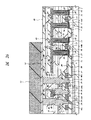
次に、スペクトル強度比(Si−N/Si−O)が5%以下の無機SOG膜を絶縁膜の一部に使用したDRAMの製造方法の一例を図6〜図36を用いて説明する。
【0037】
図6に示すように、このDRAMのメモリアレイ(MARY)は、マトリクス状に配置された複数のワード線WL(WLn-1 、WLn 、WLn+1 …)と複数のビット線BLおよびそれらの交点に配置された複数のメモリセル(MC)により構成されている。1ビットの情報を記憶する1個のメモリセルは、1個の情報蓄積用容量素子Cとこれに直列に接続された1個のメモリセル選択用MISFETQsとで構成されている。メモリセル選択用MISFETQsのソース、ドレインの一方は、情報蓄積用容量素子Cと電気的に接続され、他方はビット線BLと電気的に接続されている。ワード線WLの一端は、ワードドライバWDに接続され、ビット線BLの一端は、センスアンプSAに接続されている。
【0038】
このDRAMを製造するには、まず図7に示すように、p型で比抵抗が10Ωcm程度の半導体基板1を用意し、この半導体基板1の主面の素子分離領域をエッチングして溝を形成した後、この溝の内部に酸化シリコン膜7を埋め込んで素子分離溝5を形成する。
【0039】
次に、図8に示すように、メモリセルを形成する領域(メモリアレイ)の半導体基板1にn型不純物、例えばP(リン)をイオン打ち込みしてn型半導体領域10を形成し、メモリアレイと周辺回路の一部(nチャネル型MISFETを形成する領域)にp型不純物、例えばB(ホウ素)をイオン打ち込みしてp型ウエル11を形成し、周辺回路の他の一部(pチャネル型MISFETを形成する領域)にn型不純物、例えばP(リン)をイオン打ち込みしてn型ウエル12を形成する。n型半導体領域10は、入出力回路などから半導体基板1を通じてメモリアレイのp型ウエル11にノイズが侵入するのを防ぐために形成する。
【0040】
次に、MISFETのしきい値電圧を調整するための不純物、例えばBF2(フッ化ホウ素) )をp型ウエル11およびn型ウエル12にイオン打ち込みし、次いでp型ウエル11およびn型ウエル12の各表面をHF(フッ酸)系の洗浄液を使って除去した後、半導体基板1をウェット酸化してp型ウエル11およびn型ウエル12の各表面に清浄なゲート酸化膜13を形成する。
【0041】
次に、図9に示すように、ゲート酸化膜13の上部にゲート電極14A、14B、14Cを形成する。ゲート電極14Aは、メモリセル選択用MISFETの一部を構成し、活性領域以外の領域ではワード線WLとして機能する。また、こゲート電極14Bおよびゲート電極14Cは、周辺回路のnチャネル型MISFETおよびpチャネル型MISFETの各一部を構成する。
【0042】
ゲート電極14A(ワード線WL)およびゲート電極14B、14Cは、例えばP(リン)などのn型不純物をドープした多結晶シリコン膜を半導体基板1上にCVD法で堆積し、次いでその上部にWN(タングステンナイトライド)膜とW膜とをスパッタリング法で堆積し、さらにその上部に窒化シリコン膜15をCVD法で堆積した後、フォトレジスト膜16をマスクにしてこれらの膜をパターニングすることによって形成する。
【0043】
次に、図10に示すように、n型ウエル12にp型不純物、例えばB(ホウ素)をイオン打ち込みしてゲート電極14Cの両側のn型ウエル12にp- 型半導体領域17を形成する。また、p型ウエル11にn型不純物、例えばP(リン)をイオン打ち込みしてゲート電極14Bの両側のp型ウエル11にn- 型半導体領域18を形成し、ゲート電極14Aの両側のp型ウエル11にn型半導体領域19を形成する。これにより、メモリアレイにメモリセル選択用MISFETQsが形成される。
【0044】
次に、図11に示すように、半導体基板1上にCVD法で窒化シリコン膜20を堆積した後、メモリアレイの窒化シリコン膜20をフォトレジスト膜で覆い、周辺回路の窒化シリコン膜20を異方性エッチングすることにより、周辺回路のゲート電極14B、14Cの側壁にサイドウォールスペーサ20aを形成する。このエッチングは、ゲート酸化膜13や素子分離溝5に埋め込まれた酸化シリコン膜7の削れ量を最少とするために、酸化シリコン膜に対する窒化シリコン膜20の選択比が高くなるようなエッチングガスを使用して行う。また、ゲート電極14B、14C上の窒化シリコン膜15の削れ量を最少とするために、オーバーエッチング量を必要最小限にとどめるようにする。
【0045】
次に、周辺回路のn型ウエル12にp型不純物、例えばB(ホウ素)をイオン打ち込みしてpチャネル型MISFETのp+ 型半導体領域22(ソース、ドレイン)を形成し、周辺回路のp型ウエル11にn型不純物、例えばAs(ヒ素)をイオン打ち込みしてnチャネル型MISFETのn+ 型半導体領域23(ソース、ドレイン)を形成する。これにより、周辺回路にpチャネル型MISFETQpおよびnチャネル型MISFETQnが形成される。
【0046】
次に、図12に示すように、半導体基板1上にSOG膜24をスピン塗布してゲート電極14A(ワード線WL)のスペースをこのSOG膜24で埋め込んだ後、半導体基板1を400℃程度で熱処理してSOG膜24をベークする。このSOG膜24は、前述したFT−IRスペクトル強度比(Si−N/Si−O)が5%以下のポリシラザン系無機SOGを使用する。
【0047】
SOG膜24は、CVD法で堆積した酸化シリコン膜に比べてリフロー性が高く、微細な配線間のギャップフィル性に優れているので、ゲート電極14A(ワード線WL)のスペースがフォトリソグラフィの解像限界程度まで微細化されている場合でも、このスペースを良好に埋め込むことができる。
【0048】
また、SOG膜24は、BPSG膜などで必要とされる高温、長時間の熱処理を行わなくとも高いリフロー性が得られるため、メモリセル選択用MISFETQsのソース、ドレインや周辺回路のMISFET(nチャネル型MISFETQn、pチャネル型MISFETQp)のソース、ドレインに含まれる不純物の熱拡散を抑制して浅接合化を図ることができ、かつゲート電極14A(ワード線WL)およびゲート電極14B、14Cを構成するメタル(W膜)が熱処理時に酸化するのを抑制できるので、DRAMのメモリセルおよび周辺回路を構成するMISFETの高性能化を実現することができる。
【0049】
SOG膜24のリフロー性をさらに向上させるために、上記ポリシラザン系無機SOGにリン(P)またはホウ素(B)、あるいはそれらの両方を添加したものを使用してもよい。
【0050】
次に、図13に示すように、SOG膜24の上部に酸化シリコン膜25を堆積し、この酸化シリコン膜25をCMP法で研磨してその表面を平坦化する。酸化シリコン膜25は、例えば酸素(O2 )とテトラエトキシシラン(TEOS)とをソースガスに用いたプラズマCVD法で堆積する。
【0051】
このように、本実施の形態では、ゲート電極14A(ワード線WL)およびゲート電極14B、14Cの上部に成膜直後でも平坦性が良好なSOG膜24を塗布し、さらにその上部に堆積した酸化シリコン膜25をCMP法で平坦化する。これにより、ゲート電極14A(ワード線WL)間の微細なスペースのギャップフィル性が向上すると共に、ゲート電極14A(ワード線WL)およびゲート電極14B、14Cの上部の絶縁膜の平坦化を実現することができる。また、高温・長時間の熱処理を行わないため、メモリセルおよび周辺回路を構成するMISFETの特性劣化を防止して高性能化を実現することができる。
【0052】
次に、図14に示すように、酸化シリコン膜25の上部に酸化シリコン膜26を堆積する。この酸化シリコン膜26は、CMP法で研磨されたときに生じた前記酸化シリコン膜25の表面の微細な傷を補修するために堆積する。酸化シリコン膜26は、例えば酸素(O2 )とテトラエトキシシラン(TEOS)とをソースガスに用いたプラズマCVD法で堆積する。酸化シリコン膜25の上部には、上記酸化シリコン膜26に代えてPSG(Phospho Silicate Glass)膜などを堆積してもよい。
【0053】
次に、図15に示すように、酸化シリコン膜26の上部に形成したフォトレジスト膜27をマスクにしてメモリセル選択用MISFETQsのn型半導体領域19(ソース、ドレイン)の上部の酸化シリコン膜26、25をドライエッチングし、続いて窒化シリコン膜20をエッチングストッパに用いてSOG膜24をドライエッチングする。
【0054】
このとき、スペクトル強度比(Si−N/Si−O)が5%以下のポリシラザン系無機SOGで構成されたSOG膜24は、窒化シリコン膜20に対するエッチング選択比が高い(ゲート電極14Aの肩部で10程度、ゲート電極14Aのスペースの底部で20程度)ので、C(炭素)/F(フッ素)比の高いフルオロカーボン系のガス(C4 F8 、C3 F8 、C2 F6 など)を多く含有するエッチングガスを使用しなくとも、窒化シリコン膜20が完全に除去されないようにすることができる。
【0055】
続いて、図16に示すように、上記フォトレジスト膜27をマスクにしたドライエッチングでメモリセル選択用MISFETQsのn型半導体領域19(ソース、ドレイン)の上部の窒化シリコン膜15とゲート酸化膜13とを除去することにより、n型半導体領域19(ソース、ドレイン)の一方の上部にコンタクトホール(接続孔)28を形成し、他方の上部にコンタクトホール(接続孔)29を形成する。
【0056】
このエッチングは、酸化シリコン膜(ゲート酸化膜13および素子分離溝5内の酸化シリコン膜7)に対する窒化シリコン膜15の選択比が高くなるような条件で行い、n型半導体領域19や素子分離溝5が深く削れないようにする。また、このエッチングは、窒化シリコン膜15が異方的にエッチングされるような条件で行い、ゲート電極14A(ワード線WL)の側壁に窒化シリコン膜15が残るようにする。これにより、フォトリソグラフィの解像限界以下の微細な径を有するコンタクトホール28、29がゲート電極14A(ワード線WL)に対して自己整合で形成される。なお、コンタクトホール28、29をゲート電極14A(ワード線WL)に対して自己整合で形成するには、あらかじめ窒化シリコン膜15を異方性エッチングしてゲート電極14A(ワード線WL)の側壁にサイドウォールスペーサを形成しておいてもよい。
【0057】
このように、ゲート電極14A(ワード線WL)のスペースを埋め込むSOG膜24として、スペクトル強度比(Si−N/Si−O)が5%以下のポリシラザン系無機SOGを使用することにより、SOG膜24のエッチングが途中で停止してコンタクトホール28、29が非開孔になるといった不具合を生じることなく、SOG膜/窒化シリコン膜の選択比を向上することができる。
【0058】
次に、図17に示すように、コンタクトホール28、29の内部にプラグ30を形成し、次いで酸化シリコン膜26の上部に酸化シリコン膜31を堆積した後、半導体基板1を800℃程度で熱処理する。プラグ30は、酸化シリコン膜26の上部にn型不純物(例えばP(リン))をドープした多結晶シリコン膜をCVD法で堆積した後、この多結晶シリコン膜をCMP法で研磨してコンタクトホール28、29の内部に残すことにより形成する。また、上記熱処理によって、プラグ30を構成する多結晶シリコン膜中のn型不純物がコンタクトホール28、29の底部からメモリセル選択用MISFETQsのn型半導体領域19(ソース、ドレイン)に拡散し、n型半導体領域19が低抵抗化される。
【0059】
次に、図18に示すように、フォトレジスト膜32をマスクにしたドライエッチングで前記コンタクトホール28の上部の酸化シリコン膜31を除去してプラグ30の表面を露出させる。次に、フォトレジスト膜32を除去した後、図19に示すように、フォトレジスト膜33をマスクにしたドライエッチングで周辺回路領域の酸化シリコン膜31、26、25、SOG膜24およびゲート酸化膜13を除去することにより、nチャネル型MISFETQnのn+ 型半導体領域23(ソース、ドレイン)の上部にコンタクトホール34、35を形成し、pチャネル型MISFETQpのp+ 型半導体領域22(ソース、ドレイン)の上部にコンタクトホール36、37を形成する。
【0060】
上記のように、メモリアレイの酸化シリコン膜31を除去してプラグ30の表面を露出させるエッチングと、周辺回路領域にコンタクトホール34〜37を形成するエッチングを別工程で行うことにより、深いコンタクトホール34〜37を形成する際にプラグ30が削れるのを防ぐことができる。プラグ30の表面を露出させるエッチングとコンタクトホール34〜37を形成するエッチングは、上記と逆の順序で行ってもよい。
【0061】
次に、フォトレジスト膜33を除去した後、図20に示すように、酸化シリコン膜31の上部にビット線BLと周辺回路の第1層配線38、39とを形成する。ビット線BLおよび第1層配線38、39を形成するには、まず酸化シリコン膜31の上部にTi膜をスパッタリング法で堆積し、半導体基板1を800℃程度で熱処理する。次いで、Ti膜の上部にTiN膜をスパッタリング法で堆積し、さらにその上部にW膜と窒化シリコン膜40とをCVD法で堆積した後、フォトレジスト膜41をマスクにしてこれらの膜をパターニングする。
【0062】
酸化シリコン膜31の上部にTi膜を堆積した後、半導体基板1を800℃程度で熱処理することにより、Ti膜とSi基板とが反応し、nチャネル型MISFETQnのn+ 型半導体領域23(ソース、ドレイン)の表面とpチャネル型MISFETQpのp+ 型半導体領域22(ソース、ドレイン)の表面とに低抵抗のTiSi2 (チタンシリサイド)層42が形成される。図示は省略するが、このとき、メモリセル選択用MISFETQsのn型半導体領域19の上部のコンタクトホール28に埋め込まれたプラグ30の表面にもTiSi2 層42が形成される。これにより、n+ 型半導体領域23およびp+ 型半導体領域22に接続される配線(ビット線BL、第1層配線38、39)のコンタクト抵抗を低減することができる。また、ビット線BLをW膜/TiN膜/Ti膜で構成することにより、そのシート抵抗を2Ω/□以下にまで低減できるので、情報の読み出し速度および書き込み速度を向上させることができ、かつビット線BLと周辺回路の第1層配線38、39とを一つの工程で同時に形成することができる。さらに、周辺回路の第1層配線(38、39)をビット線BLと同層の配線で構成した場合は、第1層配線をメモリセルの上層に形成されるAl配線で構成する場合に比べて、周辺回路のMISFET(nチャネル型MISFETQn、pチャネル型MISFETQp)と第1層配線とを接続するコンタクトホール(34〜37)のアスペクト比が低減されるため、第1層配線の接続信頼性が向上する。
【0063】
次に、フォトレジスト膜41を除去した後、図21に示すように、ビット線BLの側壁と第1層配線38、39の側壁とにサイドウォールスペーサ43を形成する。サイドウォールスペーサ43は、ビット線BLおよび第1層配線38、39の上部にCVD法で窒化シリコン膜を堆積した後、この窒化シリコン膜を異方性エッチングして形成する。
【0064】
次に、図22に示すように、ビット線BLおよび第1層配線38、39の上部にSOG膜44をスピン塗布する。このSOG膜44は、前述したFT−IRスペクトル強度比(Si−N/Si−O)が5%以下のポリシラザン系無機SOGを使用してもよく、あるいはこのスペクトル強度比が5%を超える無機SOGや、有機SOGを使用してもよい。
【0065】
SOG膜44は、BPSG膜に比べてリフロー性が高く、微細な配線間のギャップフィル性に優れているので、ビット線BLのスペースを良好に埋め込むことができる。また、SOG膜44は、BPSG膜で必要とされる高温、長時間の熱処理を行わなくとも高いリフロー性が得られるため、ビット線BLの下層に形成されたメモリセル選択用MISFETQsのソース、ドレインや周辺回路のMISFET(nチャネル型MISFETQn、pチャネル型MISFETQp)のソース、ドレインに含まれる不純物の熱拡散を抑制して浅接合化を図ることができる。さらに、ゲート電極14A(ワード線WL)およびゲート電極14B、14Cを構成するメタル(W膜)の酸化を抑制できるので、DRAMのメモリセルおよび周辺回路を構成するMISFETの高性能化を実現することができる。また、ビット線BLおよび第1層配線38、39を構成するTi膜、TiN膜、W膜の酸化を抑制して配線低抵の低減を図ることができる。
【0066】
次に、図23に示すように、SOG膜44の上部に酸化シリコン膜45を堆積し、次いでこの酸化シリコン膜45をCMP法で研磨してその表面を平坦化した後、酸化シリコン膜45の上部に酸化シリコン膜46を堆積する。酸化シリコン膜45、46は、例えば酸素(O2 )とテトラエトキシシラン(TEOS)とをソースガスに用いたプラズマCVD法で堆積する。また、酸化シリコン膜46は、CMP法で研磨されたときに生じた前記酸化シリコン膜45の表面の微細な傷を補修するために堆積する。
【0067】
次に、図24に示すように、フォトレジスト膜47をマスクにしたドライエッチングでコンタクトホール29の上部の酸化シリコン膜46、45、SOG膜44および酸化シリコン膜31を除去してプラグ30の表面に達するスルーホール48を形成する。このエッチングは、酸化シリコン膜46、45、31およびSOG膜44に対する窒化シリコン膜のエッチングレートが小さくなるような条件で行い、スルーホール48とビット線BLの合わせずれが生じた場合でも、ビット線BLの上部の窒化シリコン膜40やサイドウォールスペーサ43が深く削れないようにする。これにより、スルーホール48がビット線BLに対して自己整合で形成される。
【0068】
次に、図25に示すように、スルーホール48の内部にプラグ49を形成する。プラグ49は、酸化シリコン膜46の上部にn型不純物(例えばP(リン))をドープした多結晶シリコン膜をCVD法で堆積した後、この多結晶シリコン膜をエッチバックしてスルーホール48の内部に残すことにより形成する。
【0069】
次に、図26に示すように、酸化シリコン膜46の上部に窒化シリコン膜51をCVD法で堆積した後、フォトレジスト膜52をマスクにしたドライエッチングで周辺回路領域の窒化シリコン膜51を除去する。メモリアレイに残った窒化シリコン膜51は、後述する情報蓄積用容量素子の下部電極を形成する工程で下部電極の間の酸化シリコン膜をエッチングする際のエッチングストッパとして使用される。
【0070】
次に、フォトレジスト膜52を除去した後、図27に示すように、窒化シリコン膜51の上部に酸化シリコン膜53を堆積し、フォトレジスト膜54をマスクにしたドライエッチングで酸化シリコン膜53および窒化シリコン膜51を除去することにより、スルーホール48の上部に溝55を形成する。このとき同時に、メモリアレイの周囲にメモリアレイを取り囲む枠状の溝55aを形成する。酸化シリコン膜53は、例えば酸素(O2 )とテトラエトキシシラン(TEOS)とをソースガスに用いたプラズマCVD法で堆積する。
【0071】
次に、フォトレジスト膜54を除去した後、図28に示すように、酸化シリコン膜53の上部に、情報蓄積用容量素子の下部電極材料として使用されるn型不純物(例えばP(リン))をドープした多結晶シリコン膜56をCVD法で堆積した後、多結晶シリコン膜56の上部に溝55、55aを埋め込むのに十分な膜厚のSOG膜57をスピン塗布し、次いで400℃程度の熱処理でSOG膜57をベークする。このSOG膜57は、前述したFT−IRスペクトル強度比(Si−N/Si−O)が5%以下のポリシラザン系無機SOGを使用してもよく、あるいはこのスペクトル強度比が5%を超える無機SOG)や、有機SOGを使用してもよい。
【0072】
次に、図29に示すように、SOG膜57をエッチバックし、さらに酸化シリコン膜53の上部の多結晶シリコン膜56をエッチバックすることにより、溝55、55aの内側(内壁および底部)に多結晶シリコン膜56を残す。
【0073】
次に、図30に示すように、周辺回路領域の酸化シリコン膜53をフォトレジスト膜58で覆い、溝55の内部のSOG膜57と溝55の隙間の酸化シリコン膜53とをウェットエッチングで除去することにより、情報蓄積用容量素子の下部電極60を形成する。このとき、溝55の隙間には窒化シリコン膜51が残っているので、この隙間の酸化シリコン膜46がエッチングされることはない。また、周辺回路領域の酸化シリコン膜53を覆うフォトレジスト膜58の一端は、メモリアレイの最も外側に形成される下部電極60と周辺回路領域との境界部、すなわち溝55aの上部に配置される。このようにすると、フォトレジスト膜58に合わせずれが生じた場合でも、その端部がメモリアレイの最も外側に形成される下部電極60上に位置することがないので、この下部電極60の溝55の内部にSOG膜57が残ったり、この下部電極60と溝55aとの隙間に酸化シリコン膜53が残ったりすることはない。また、周辺回路領域の酸化シリコン膜53の一部がエッチング液に曝されることもないので、周辺回路領域の酸化シリコン膜53の一部が削れて深い溝ができたりすることもない。
【0074】
次に、フォトレジスト膜58を除去し、次いで下部電極60を構成する多結晶シリコン膜(56)の酸化を防止するために、半導体基板1をアンモニア雰囲気中、800℃程度で熱処理して多結晶シリコン膜(56)の表面を窒化した後、図31に示すように、下部電極60の上部にTa2 O5(酸化タンタル) 膜61をCVD法で堆積し、次いで半導体基板1を800℃程度で熱処理してTa2 O5 膜61の欠陥を修復した後、Ta2 O5 膜61の上部にCVD法とスパッタリング法とでTiN膜62を堆積し、フォトレジスト膜63をマスクにしたドライエッチングでTiN膜62およびTa2 O5 膜61をパターニングすることにより、TiN膜62からなる上部電極と、Ta2 O5 膜61からなる容量絶縁膜と、多結晶シリコン膜56からなる下部電極60とで構成される情報蓄積用容量素子Cを形成する。これにより、メモリセル選択用MISFETQsとこれに直列に接続された情報蓄積用容量素子Cとで構成されるDRAMのメモリセルが完成する。
【0075】
次に、フォトレジスト膜63を除去した後、図32に示すように、情報蓄積用容量素子Cの上部に膜厚100nm程度の酸化シリコン膜64を堆積する。酸化シリコン膜65は、例えば酸素(O2 )とテトラエトキシシラン(TEOS)とをソースガスに用いたプラズマCVD法で堆積する。続いて、フォトレジスト膜65をマスクにしたドライエッチングで周辺回路の第1層配線38の上部の酸化シリコン膜64、53、46、45、SOG膜44および窒化シリコン膜40を除去することにより、スルーホール66を形成する。
【0076】
次に、フォトレジスト膜65を除去した後、図33に示すように、スルーホール66の内部にプラグ67を形成し、続いて酸化シリコン膜64の上部に第2層配線68、69を形成する。プラグ67は、酸化シリコン膜64の上部にスパッタリング法でTiN膜を堆積し、さらにその上部にCVD法でW膜を堆積した後、これらの膜をエッチバックしてスルーホール66の内部に残すことにより形成する。第2層配線68、69は、酸化シリコン膜64の上部にスパッタリング法でTiN膜、Al(アルミニウム)膜、TiN膜を順次堆積した後、フォトレジスト膜をマスクにしたドライエッチングでこれらの膜をパターニングして形成する。
【0077】
次に、図34に示すように、第2層配線68、69の上部に層間絶縁膜を堆積する。層間絶縁膜は、例えばSOG膜72および酸化シリコン膜73の積層膜で構成する。SOG膜72は、前述したFT−IRスペクトル強度比(Si−N/Si−O)が5%以下のポリシラザン系無機SOGを使用してスピン塗布し、酸化シリコン膜73は、例えば酸素(O2 )とテトラエトキシシラン(TEOS)とをソースガスに用いたプラズマCVD法で堆積する。
【0078】
次に、図35に示すように、情報蓄積用容量素子Cの上部の層間絶縁膜にスルーホール(接続孔)74を形成し、周辺回路の第2層配線69の上部の層間絶縁膜にスルーホール(接続孔)75を形成する。スルーホール74、75は、フォトレジスト膜をマスクにしたドライエッチングで酸化シリコン膜73およびSOG膜72を除去することにより形成する。
【0079】
上記スルーホール74、75を形成するためのドライエッチングでは、スルーホール75の底部に第2層配線69の表面が露出する。この第2層配線69の最上層はTiN膜で構成されているために、第2層配線69を覆う層間絶縁膜の一部を構成するSOG膜72として、窒化シリコン膜に対するドライエッチング選択比が低いSOG材料(例えばスペクトル強度比(Si−N/Si−O)が5%を超えるポリシラザン系無機SOG)を使用すると、窒化シリコン膜と同様に窒素を含有するTiN膜がオーバーエッチングされてAl膜が露出する。すると、次の工程でスルーホール74、75の内部にプラグを埋め込む際、その前処理としてスルーホール74、75の内部を洗浄したときに、Al膜が洗浄液に晒されて腐蝕を引き起こすことがある。
【0080】
ところが、SOG膜72として、窒化シリコン膜に対するドライエッチング選択比が高い材料、すなわちスペクトル強度比(Si−N/Si−O)が5%以下のポリシラザン系無機SOGを使用した場合には、窒化シリコン膜と同じく含窒素化合物であるTiN膜がオーバーエッチングされてAl膜が露出するのを防ぐことができるので、第2層配線69の腐蝕による断線などを防止することができる。なお、第2層配線69の最上層をTiN膜に代えて他の窒化金属膜(例えばWN膜)で構成した場合でも、同様の効果(Al膜の腐蝕防止)を得ることができる。
【0081】
次に、図36に示すように、スルーホール74、75の内部にプラグ76を形成し、続いて層間絶縁膜の上部に第3層配線77、78、79を形成する。プラグ76は、層間絶縁膜の上部にスパッタリング法でTiN膜を堆積し、さらにその上部にCVD法でW膜を堆積した後、これらの膜をエッチバックしてスルーホール74、75の内部に残すことにより形成する。第3層配線77〜79は、層間絶縁膜の上部にスパッタリング法でTiN膜、Al膜、TiN膜を堆積した後、フォトレジスト膜をマスクにしたドライエッチングでこれらの膜をパターニングして形成する。
【0082】
その後、第3層配線77〜79の上部に酸化シリコン膜と窒化シリコン膜とで構成されたパッシベーション膜を堆積するが、その図示は省略する。以上の工程により、本実施の形態のDRAMが略完成する。
【0083】
以上、本発明者によってなされた発明を発明の実施の形態に基づき具体的に説明したが、本発明は前記実施の形態に限定されるものではなく、その要旨を逸脱しない範囲で種々変更可能であることは言うまでもない。
【0084】
前記実施の形態では、DRAMの製造プロセスに適用した場合について説明したが、本発明は、メモリLSIやロジックLSIを問わず、一般に微細な間隔で形成された電極配線のスペースにSOG膜を埋め込むプロセスを有する高集積LSIに広く適用することができる。
【0085】
【発明の効果】
本願において開示される発明のうち、代表的なものによって得られる効果を簡単に説明すれば以下のとおりである。
【0086】
本発明によれば、窒化シリコン膜をエッチングストッパに用いたSAC(セルフアラインコンタクト)技術を利用し電極配線のスペースに埋め込んだSOG膜にコンタクトホールを形成する際に、コンタクトホールの非開孔を生じることなく、SOG膜/窒化シリコン膜の選択比を向上することができる。
【0087】
本発明によれば、少なくともその上部に窒化金属膜が積層されたAl系の導電膜からなる配線の上部にSOG膜を含んだ層間絶縁膜を形成し、この層間絶縁膜をドライエッチングしてこの配線の上部に接続孔を形成する際に、窒化金属膜がオーバーエッチングされてAl系の導電膜が接続孔の底部に露出するのを防ぐことができるので、配線腐蝕を防止することができる。
【図面の簡単な説明】
【図1】ポリシラザン系の無機SOGの分子構造を示す模式図である。
【図2】酸化反応促進剤の添加量を変えた原料ポリマーをシリコン基板上にスピン塗布してベーク処理した結果得られた無機SOG膜のFT−IRスペクトル強度比(Si−N/Si−O)を示すグラフである。
【図3】(a)、(b)は、無機SOG膜の対p−TEOS膜エッチング速度比を調べるために行ったテスト方法を示す半導体基板の要部断面図である。
【図4】フォトレジスト膜の孔径とエッチング深さとの関係を、無機SOG膜を使用した場合とp−TEOS膜を使用した場合とでそれぞれ測定した結果を示すグラフである。
【図5】無機SOG膜の対p−TEOS膜エッチング速度比を調べるために行ったテスト結果を示すグラフである。
【図6】本発明の一実施の形態であるDRAMの回路図である。
【図7】本発明の一実施の形態であるDRAMの製造方法を示す半導体基板の要部断面図である。
【図8】本発明の一実施の形態であるDRAMの製造方法を示す半導体基板の要部断面図である。
【図9】本発明の一実施の形態であるDRAMの製造方法を示す半導体基板の要部断面図である。
【図10】本発明の一実施の形態であるDRAMの製造方法を示す半導体基板の要部断面図である。
【図11】本発明の一実施の形態であるDRAMの製造方法を示す半導体基板の要部断面図である。
【図12】本発明の一実施の形態であるDRAMの製造方法を示す半導体基板の要部断面図である。
【図13】本発明の一実施の形態であるDRAMの製造方法を示す半導体基板の要部断面図である。
【図14】本発明の一実施の形態であるDRAMの製造方法を示す半導体基板の要部断面図である。
【図15】本発明の一実施の形態であるDRAMの製造方法を示す半導体基板の要部断面図である。
【図16】本発明の一実施の形態であるDRAMの製造方法を示す半導体基板の要部断面図である。
【図17】本発明の一実施の形態であるDRAMの製造方法を示す半導体基板の要部断面図である。
【図18】本発明の一実施の形態であるDRAMの製造方法を示す半導体基板の要部断面図である。
【図19】本発明の一実施の形態であるDRAMの製造方法を示す半導体基板の要部断面図である。
【図20】本発明の一実施の形態であるDRAMの製造方法を示す半導体基板の要部断面図である。
【図21】本発明の一実施の形態であるDRAMの製造方法を示す半導体基板の要部断面図である。
【図22】本発明の一実施の形態であるDRAMの製造方法を示す半導体基板の要部断面図である。
【図23】本発明の一実施の形態であるDRAMの製造方法を示す半導体基板の要部断面図である。
【図24】本発明の一実施の形態であるDRAMの製造方法を示す半導体基板の要部断面図である。
【図25】本発明の一実施の形態であるDRAMの製造方法を示す半導体基板の要部断面図である。
【図26】本発明の一実施の形態であるDRAMの製造方法を示す半導体基板の要部断面図である。
【図27】本発明の一実施の形態であるDRAMの製造方法を示す半導体基板の要部断面図である。
【図28】本発明の一実施の形態であるDRAMの製造方法を示す半導体基板の要部断面図である。
【図29】本発明の一実施の形態であるDRAMの製造方法を示す半導体基板の要部断面図である。
【図30】本発明の一実施の形態であるDRAMの製造方法を示す半導体基板の要部断面図である。
【図31】本発明の一実施の形態であるDRAMの製造方法を示す半導体基板の要部断面図である。
【図32】本発明の一実施の形態であるDRAMの製造方法を示す半導体基板の要部断面図である。
【図33】本発明の一実施の形態であるDRAMの製造方法を示す半導体基板の要部断面図である。
【図34】本発明の一実施の形態であるDRAMの製造方法を示す半導体基板の要部断面図である。
【図35】本発明の一実施の形態であるDRAMの製造方法を示す半導体基板の要部断面図である。
【図36】本発明の一実施の形態であるDRAMの製造方法を示す半導体基板の要部断面図である。
【符号の説明】
1 半導体基板
1A 半導体チップ
2 SOG膜
3 酸化シリコン膜
4 フォトレジスト膜
5 素子分離溝
6 酸化シリコン(p−TEOS)膜
7 酸化シリコン膜
10 n型半導体領域
11 p型ウエル
12 n型ウエル
13 ゲート酸化膜
14A〜14C ゲート電極
15 窒化シリコン膜
16 フォトレジスト膜
17 p- 型半導体領域
18 n- 型半導体領域
19 n型半導体領域
20 窒化シリコン膜
20a サイドウォールスペーサ
22 p+ 型半導体領域
23 n+ 型半導体領域
24 SOG(スピンオングラス)膜
25 酸化シリコン膜
26 酸化シリコン膜
27 フォトレジスト膜
28 コンタクトホール(接続孔)
29 コンタクトホール(接続孔)
30 プラグ
31 酸化シリコン膜
32 フォトレジスト膜
33 フォトレジスト膜
34〜37 コンタクトホール
38、39 第1層配線
40 窒化シリコン膜
41 フォトレジスト膜
42 TiSi2 層
43 サイドウォールスペーサ
44 SOG膜
45 酸化シリコン膜
46 酸化シリコン膜
47 フォトレジスト膜
48 スルーホール
49 プラグ
51 窒化シリコン膜
52 フォトレジスト膜
53 酸化シリコン膜
54 フォトレジスト膜
55 溝
55a 溝
56 多結晶シリコン膜
57 SOG膜
58 フォトレジスト膜
60 下部電極
61 Ta2 O5(酸化タンタル) 膜
62 TiN膜(上部電極)
63 フォトレジスト膜
64 酸化シリコン膜
65 フォトレジスト膜
66 スルーホール
67 プラグ
68、69 第2層配線
72 SOG膜
73 酸化シリコン膜
74、75 スルーホール(接続孔)
76 プラグ
77〜79 第3層配線
BL ビット線
C 情報蓄積用容量素子
MARY メモリアレイ
Qn nチャネル型MISFET
Qp pチャネル型MISFET
Qs メモリセル選択用MISFET
SA センスアンプ
WD ワードドライバ[0001]
BACKGROUND OF THE INVENTION
The present invention relates to a manufacturing technique of a semiconductor integrated circuit device, and more particularly, to a gate of a MISFET (Metal Insulator Semiconductor Field Effect Transistor) using a self-alignment contact (SAC) technique using a silicon nitride film as an etching stopper. The present invention relates to a technique effective when applied to a process of forming a fine contact hole between electrodes.
[0002]
[Prior art]
A DRAM (Dynamic Random Access Memory) memory cell is arranged at the intersection of a plurality of word lines and a plurality of bit lines arranged in a matrix on the main surface of a semiconductor substrate. It is composed of one memory cell selection MISFET (Metal Insulator Semiconductor Field Effect Transistor) connected in series. The memory cell selection MISFET is formed in an active region surrounded by an element isolation region, and is mainly composed of a gate oxide film, a gate electrode integrated with a word line, and a pair of semiconductor regions constituting a source and a drain. Has been. The bit line is disposed above the memory cell selection MISFET and is electrically connected to one of the source and the drain shared by the two memory cell selection MISFETs adjacent in the extending direction. The information storage capacitive element is also disposed above the memory cell selection MISFET and is electrically connected to the other of the source and drain.
[0003]
As described above, in a DRAM memory cell, a bit line and an information storage capacitor are arranged above the word line, and a plurality of layers of Al (aluminum) wiring are usually arranged above the memory cell. The Therefore, steps due to these electrodes and wirings are inevitably generated in the area of the memory array. In addition, a level difference corresponding to the height of the information storage capacitive element is generated between the area where the memory array is formed (memory array) and the peripheral circuit area.
[0004]
However, if the wiring is formed on such a step, the exposure light may be defocused during photolithography, or etching residue may be generated in the step portion. Defects such as disconnection occur. Therefore, in order to solve these problems, a flattening technique of an interlayer insulating film that insulates the lower layer wiring from the upper layer wiring is indispensable.
[0005]
For the planarization of the interlayer insulating film, a method using a BPSG (Boron-doped Phospho Silicate Glass) film or SOG (Spin On Glass) film having high reflow properties, chemical mechanical polishing (CMP), or the like. ) Various methods have been developed.
[0006]
For example, Japanese Patent Laid-Open No. 9-64303 discloses a DRAM having a capacitor over bitline structure in which an information storage capacitive element is arranged above a bit line. The DRAM described in this publication uses a BPSG film as an insulating film between a word line (gate electrode) and an upper bit line, and an insulating film between the bit line and an information storage capacitor above the bit line. In this way, the insulating film is flattened. Further, this DRAM has a memory array and a peripheral circuit region by forming an insulating film between the information storage capacitor element and the Al wiring thereabove as a three-layer film of a silicon oxide film, an SOG film and a silicon oxide film. The level difference between the two is reduced.
[0007]
In addition, the DRAM described in Japanese Patent Laid-Open No. 9-45766 uses a highly reflowable BPSG film containing B (boron) at a high concentration (about 13 mol%), so that the memory array and the peripheral circuit region are separated. The reduction of the level | step difference produced between is aimed at.
[0008]
[Problems to be solved by the invention]
In the prior art described in the above publication, the insulating film between the word line (gate electrode) and the bit line above the word line (gate electrode) is formed of a BPSG film, so that the insulating film caused by the step of the word line (gate electrode) The level difference is flattened.
[0009]
However, in a DRAM of 256 Mbit (megabit) or later, the gate length of the memory cell selection MISFET constituting the memory cell is 0.25 μm or less, and the space between adjacent word lines (gate electrodes) is equal to or less than that. Therefore, even if the BPSG film is reflowed at a high temperature for a long time, it becomes difficult to completely eliminate voids generated in this space, and the flatness of the insulating film above the word line (gate electrode) is ensured. Can not be.
[0010]
Therefore, in a DRAM of 256 Mbit or more, a void is generated in the space of the word line (gate electrode) by configuring the insulating film above the word line (gate electrode) with an SOG film having a reflow property higher than that of the BPSG film. It is considered that a technique for embedding an insulating film is essential.
[0011]
However, on the other hand, when the insulating film above the word line (gate electrode) is composed of an SOG film, the SAC (self-aligned contact) technique using a silicon nitride film as an etching stopper is used to form a space for the gate electrode. When forming a fine contact hole, the problem is how to improve the selectivity of the SOG film, which has a smaller selectivity of the silicon nitride film than the BPSG film.
[0012]
That is, when the SOG film / silicon nitride film selection ratio is small, the silicon nitride sidewall spacer formed on the side wall of the gate electrode is over-etched with sputter ions, so that the contact hole and the gate electrode are short-circuited. End up. On the other hand, a fluorocarbon-based gas having a high C (carbon) / F (fluorine) ratio (C Four F 8 , C Three F 8 , C 2 F 6 When an etching gas containing a large amount of gas is used to increase the SOG film / silicon nitride film selection ratio, the fluorocarbon-based protective film generated by the etching reaction is deposited on the surface of the SOG film. This causes a problem that the etching of the SOG film stops in the middle and the contact hole cannot be formed.
[0013]
An object of the present invention is to form a non-opening of a contact hole when a contact hole is formed in an SOG film embedded in a space of a gate electrode using a SAC (self-aligned contact) technique using a silicon nitride film as an etching stopper. It is an object of the present invention to provide a technique capable of improving the SOG film / silicon nitride film selection ratio without causing the above-described problem.
[0014]
The above and other objects and novel features of the present invention will be apparent from the description of this specification and the accompanying drawings.
[0015]
[Means for Solving the Problems]
Of the inventions disclosed in the present application, the outline of typical ones will be briefly described as follows.
[0016]
(1) The method for manufacturing a semiconductor integrated circuit device of the present invention includes the following steps (a) to (c).
[0017]
(A) a step of depositing a silicon nitride film on top of the plurality of electrode wirings after forming a plurality of electrode wirings on the main surface of the semiconductor substrate;
(B) An inorganic SOG film having a ratio of Si—N bonds to Si—O bonds of 5% or less (infrared spectral intensity ratio conversion) is spin-coated on the plurality of electrode wirings covered with the silicon nitride film. Burying the inorganic SOG film in a space between the plurality of electrode wirings,
(C) A step of forming a connection hole in a space between the plurality of electrode wirings by dry etching the inorganic SOG film using the silicon nitride film as an etching stopper.
[0018]
(2) The method for manufacturing a semiconductor integrated circuit device of the present invention includes the following steps (a) to (c).
[0019]
(A) forming a plurality of MISFET gate electrodes on the main surface of the semiconductor substrate, and then depositing a silicon nitride film on the plurality of gate electrodes;
(B) On top of the plurality of gate electrodes covered with the silicon nitride film, an inorganic SOG film having a Si—N bond to Si—O bond ratio of 5% or less (infrared spectral intensity ratio conversion) is spin-coated. Burying the inorganic SOG film in a space between the plurality of gate electrodes,
(C) forming a connection hole in a space between the plurality of gate electrodes by dry etching the inorganic SOG film using the silicon nitride film as an etching stopper;
[0020]
(3) In the method of manufacturing a semiconductor integrated circuit device according to the present invention, the plurality of MISFETs are memory cell selection MISFETs constituting a part of a DRAM memory cell.
[0021]
(4) In the method for manufacturing a semiconductor integrated circuit device according to the present invention, the connection hole electrically connects one of the source and drain of the memory cell selection MISFET and a bit line, and At least one of the second connection holes for electrically connecting the other of the source and drain of the memory cell selection MISFET and the information storage capacitive element constituting the other part of the memory cell of the DRAM.
[0022]
(5) In the method for manufacturing a semiconductor integrated circuit device of the present invention, the diameter of the bottom of the connection hole is not more than the minimum dimension determined by the resolution limit of photolithography.
[0023]
(6) The method for manufacturing a semiconductor integrated circuit device of the present invention includes the following steps (a) to (c).
[0024]
(A) forming a wiring made of an aluminum-based conductive film in which a metal nitride film is laminated at least on the main surface of the semiconductor substrate;
(B) By spin-coating an inorganic SOG film having a Si—N bond to Si—O bond ratio of 5% or less (infrared spectral intensity ratio conversion) on the upper part of the wiring, the inorganic SOG is formed on the upper part of the wiring. Forming an interlayer insulating film including a film;
(C) A step of forming a connection hole for electrically connecting the wiring and an upper layer wiring thereon by dry etching the interlayer insulating film including the inorganic SOG film.
[0025]
(7) In the method of manufacturing a semiconductor integrated circuit device according to the present invention, a ratio of Si—N bonds to Si—O bonds is 5% or less (infrared spectrum intensity) by adding an oxidation reaction accelerator to polysilazane inorganic SOG. (In terms of ratio) inorganic SOG is obtained.
[0026]
(8) In the method of manufacturing a semiconductor integrated circuit device according to the present invention, phosphorus, boron, or both are added to the inorganic SOG film.
[0027]
DETAILED DESCRIPTION OF THE INVENTION
Hereinafter, embodiments of the present invention will be described in detail with reference to the drawings. Note that components having the same function are denoted by the same reference symbols throughout the drawings for describing the embodiments, and the repetitive description thereof will be omitted.
[0028]
FIG. 1 is a schematic diagram showing the molecular structure of a polysilazane-based inorganic SOG (spin-on-glass). As shown in the figure, polysilazane-based inorganic SOG is obtained by baking a raw polymer whose basic skeleton is composed of Si—N bonds in an atmosphere containing oxygen and water, and replacing the Si—N bonds with Si—O bonds. Is obtained. However, at this time, not all Si—N bonds are replaced by Si—O bonds, and normally, about 10 to 10% of Si in terms of FT-IR spectral intensity ratio (Si—N / Si—O). An inorganic SOG film in which —N bonds remain is obtained.
[0029]
The inventor added an oxidation reaction accelerator to the raw material polymer and baked, whereby the ratio of Si—N / Si—O (FT-IR spectral intensity ratio, the same applies hereinafter) was 5% or less. An inorganic SOG film was prepared. Although methyl alcohol was mainly used as the oxidation reaction accelerator, similar results were obtained when other lower alcohols (such as ethyl alcohol and propyl alcohol) were added.
[0030]
FIG. 2 shows three types of inorganic SOG films (a), (b), and (c) obtained as a result of spin-coating a raw material polymer with a different amount of addition of an oxidation reaction accelerator on a silicon substrate and baking it. It is a graph which shows FT-IR spectrum intensity ratio (Si-N / Si-O). In the figure, the horizontal axis shows the wave number (Wave Number) of IR, the vertical axis shows the spectrum intensity (Intensity), and the broken line in the figure shows the spectrum of Si—N bonds (wave number˜900). The spectral intensity ratios (Si—N / Si—O) of these three kinds of inorganic SOG films (a), (b), and (c) are 1.1%, 3.4%, and 20.4%, respectively. .
[0031]
Next, as shown in FIG. 3A, a single crystal
[0032]
As a comparative example, as shown in FIG. 2 ) And tetraethoxysilane as a source gas by a plasma CVD method, a silicon oxide film (p-TEOS)
[0033]
Next, the relationship between the hole diameter of the
[0034]
FT-IR spectral intensity ratios (Si-N / Si-O) of the three types of inorganic SOG films (a), (b), and (c) obtained from FIG. FIG. 5 shows the relationship between the inorganic SOG films (a), (b) and (c) versus the p-TEOS film etching rate ratio. From this graph, as the spectral intensity ratio (Si—N / Si—O) of the inorganic SOG film decreases, the etching rate approaches that of the p-TEOS film, and when the spectral intensity ratio becomes 5% or less, the p-TEOS film It can be seen that the etching rate ratio is 0.6 or more.
[0035]
From the above, by using an inorganic SOG film having a spectral intensity ratio (Si-N / Si-O) of 5% or less, the selectivity ratio of the SOG film / silicon nitride film can be improved, and this spectral intensity ratio ( It was found that the smaller the Si—N / Si—O), the more the selectivity can be improved.
[0036]
Next, an example of a DRAM manufacturing method using an inorganic SOG film having a spectral intensity ratio (Si—N / Si—O) of 5% or less as a part of an insulating film will be described with reference to FIGS.
[0037]
As shown in FIG. 6, the DRAM memory array (MARY) includes a plurality of word lines WL (WLn-1, WLn, WLn + 1...) And a plurality of bit lines BL arranged in a matrix and their intersections. Are constituted by a plurality of memory cells (MC). One memory cell that stores 1-bit information is composed of one information storage capacitor C and one memory cell selection MISFET Qs connected in series therewith. One of the source and drain of the memory cell selection MISFET Qs is electrically connected to the information storage capacitor C, and the other is electrically connected to the bit line BL. One end of the word line WL is connected to the word driver WD, and one end of the bit line BL is connected to the sense amplifier SA.
[0038]
In order to manufacture this DRAM, first, as shown in FIG. 7, a p-
[0039]
Next, as shown in FIG. 8, an n-
[0040]
Next, an impurity for adjusting the threshold voltage of the MISFET, for example, BF 2 (Boron fluoride)) is ion-implanted into the p-
[0041]
Next, as shown in FIG. 9, gate electrodes 14 </ b> A, 14 </ b> B, and 14 </ b> C are formed on the
[0042]
As the
[0043]
Next, as shown in FIG. 10, a p-type impurity, for example, B (boron) is ion-implanted into the n-
[0044]
Next, as shown in FIG. 11, after depositing a
[0045]
Next, a p-type impurity, for example, B (boron) is ion-implanted into the n-type well 12 of the peripheral circuit, and the p-channel MISFET p. + Type semiconductor region 22 (source, drain) is formed, and an n-type impurity, for example, As (arsenic) is ion-implanted into the p-type well 11 of the peripheral circuit to form the n-channel MISFET n. + A type semiconductor region 23 (source, drain) is formed. Thereby, the p-channel type MISFET Qp and the n-channel type MISFET Qn are formed in the peripheral circuit.
[0046]
Next, as shown in FIG. 12, an
[0047]
Since the
[0048]
Further, since the
[0049]
In order to further improve the reflow property of the
[0050]
Next, as shown in FIG. 13, a
[0051]
As described above, in this embodiment, the
[0052]
Next, as shown in FIG. 14, a
[0053]
Next, as shown in FIG. 15, using the
[0054]
At this time, the
[0055]
Subsequently, as shown in FIG. 16, the
[0056]
This etching is performed under the condition that the selection ratio of the
[0057]
As described above, by using a polysilazane inorganic SOG having a spectral intensity ratio (Si—N / Si—O) of 5% or less as the
[0058]
Next, as shown in FIG. 17, a
[0059]
Next, as shown in FIG. 18, the
[0060]
As described above, a deep contact hole is obtained by performing etching for removing the
[0061]
Next, after the
[0062]
After the Ti film is deposited on the
[0063]
Next, after removing the
[0064]
Next, as shown in FIG. 22, the
[0065]
Since the
[0066]
Next, as shown in FIG. 23, a
[0067]
Next, as shown in FIG. 24, the
[0068]
Next, as shown in FIG. 25, a
[0069]
Next, as shown in FIG. 26, after a
[0070]
Next, after removing the
[0071]
Next, after removing the
[0072]
Next, as shown in FIG. 29, the
[0073]
Next, as shown in FIG. 30, the
[0074]
Next, the
[0075]
Next, after removing the
[0076]
Next, after removing the
[0077]
Next, as shown in FIG. 34, an interlayer insulating film is deposited on the
[0078]
Next, as shown in FIG. 35, a through hole (connection hole) 74 is formed in the interlayer insulating film above the information storage capacitor element C, and the through hole is formed in the interlayer insulating film above the
[0079]
In the dry etching for forming the through
[0080]
However, when a material having a high dry etching selectivity with respect to the silicon nitride film, that is, a polysilazane inorganic SOG having a spectral intensity ratio (Si—N / Si—O) of 5% or less is used as the
[0081]
Next, as shown in FIG. 36, plugs 76 are formed in the through
[0082]
Thereafter, a passivation film composed of a silicon oxide film and a silicon nitride film is deposited on the third layer wirings 77 to 79, but the illustration thereof is omitted. Through the above steps, the DRAM of this embodiment is substantially completed.
[0083]
As mentioned above, the invention made by the present inventor has been specifically described based on the embodiments of the invention. However, the present invention is not limited to the above-described embodiments, and various modifications can be made without departing from the scope of the invention. Needless to say.
[0084]
In the above-described embodiment, the case where the present invention is applied to a DRAM manufacturing process has been described. It can be widely applied to highly integrated LSIs having
[0085]
【The invention's effect】
Among the inventions disclosed in the present application, effects obtained by typical ones will be briefly described as follows.
[0086]
According to the present invention, when the contact hole is formed in the SOG film embedded in the electrode wiring space using the SAC (self-aligned contact) technique using the silicon nitride film as an etching stopper, the non-opening of the contact hole is formed. The SOG film / silicon nitride film selection ratio can be improved without the occurrence.
[0087]
According to the present invention, an interlayer insulating film including an SOG film is formed at least on the wiring made of an Al-based conductive film having a metal nitride film laminated thereon, and the interlayer insulating film is dry-etched. When forming the connection hole in the upper part of the wiring, it is possible to prevent the metal nitride film from being over-etched and exposing the Al-based conductive film to the bottom of the connection hole, so that the wiring corrosion can be prevented.
[Brief description of the drawings]
FIG. 1 is a schematic diagram showing the molecular structure of a polysilazane-based inorganic SOG.
FIG. 2 shows a FT-IR spectrum intensity ratio (Si—N / Si—O) of an inorganic SOG film obtained as a result of spin-coating a raw material polymer with a different addition amount of an oxidation reaction accelerator on a silicon substrate and baking it. ).
FIGS. 3A and 3B are cross-sectional views of a principal part of a semiconductor substrate showing a test method performed for examining an etching rate ratio of an inorganic SOG film to a p-TEOS film. FIGS.
FIG. 4 is a graph showing results of measuring the relationship between the hole diameter and etching depth of a photoresist film when an inorganic SOG film is used and when a p-TEOS film is used.
FIG. 5 is a graph showing the results of a test performed to examine the etching rate ratio of an inorganic SOG film to a p-TEOS film.
FIG. 6 is a circuit diagram of a DRAM according to an embodiment of the present invention.
FIG. 7 is a fragmentary cross-sectional view of a semiconductor substrate showing a method of manufacturing a DRAM according to an embodiment of the present invention.
FIG. 8 is a fragmentary cross-sectional view of a semiconductor substrate showing a method for manufacturing a DRAM according to an embodiment of the present invention;
FIG. 9 is a fragmentary cross-sectional view of a semiconductor substrate showing a method of manufacturing a DRAM according to an embodiment of the present invention.
FIG. 10 is a cross sectional view of the essential part of the semiconductor substrate, for illustrating a method for manufacturing a DRAM according to an embodiment of the present invention.
FIG. 11 is a fragmentary cross-sectional view of a semiconductor substrate showing a method of manufacturing a DRAM which is an embodiment of the present invention;
FIG. 12 is a fragmentary cross-sectional view of a semiconductor substrate showing a method of manufacturing a DRAM according to an embodiment of the present invention.
FIG. 13 is a fragmentary cross-sectional view of a semiconductor substrate showing a method of manufacturing a DRAM according to an embodiment of the present invention.
FIG. 14 is a fragmentary cross-sectional view of a semiconductor substrate showing a method of manufacturing a DRAM according to an embodiment of the present invention.
FIG. 15 is a cross sectional view of the essential part of the semiconductor substrate, showing a method for manufacturing a DRAM according to an embodiment of the present invention.
FIG. 16 is a fragmentary cross-sectional view of a semiconductor substrate showing a method of manufacturing a DRAM which is an embodiment of the present invention;
FIG. 17 is a cross sectional view of the essential part of the semiconductor substrate, showing a method for manufacturing a DRAM according to an embodiment of the present invention.
FIG. 18 is a cross sectional view for a main portion of a semiconductor substrate, showing a method for manufacturing a DRAM according to an embodiment of the present invention;
FIG. 19 is a cross sectional view of the essential part of the semiconductor substrate, showing a method for manufacturing a DRAM according to an embodiment of the present invention.
FIG. 20 is a fragmentary cross-sectional view of the semiconductor substrate showing the method of manufacturing the DRAM according to the embodiment of the present invention.
FIG. 21 is a cross sectional view of the essential part of the semiconductor substrate, for illustrating a method for manufacturing a DRAM according to an embodiment of the present invention.
FIG. 22 is a fragmentary cross-sectional view of the semiconductor substrate, illustrating the method for manufacturing the DRAM according to one embodiment of the present invention.
FIG. 23 is a cross sectional view of the essential part of the semiconductor substrate, for illustrating a method for manufacturing a DRAM according to an embodiment of the present invention.
FIG. 24 is a cross sectional view of the essential part of the semiconductor substrate, for illustrating a method for manufacturing a DRAM according to an embodiment of the present invention.
FIG. 25 is a cross sectional view of the essential part of the semiconductor substrate, showing a method for manufacturing a DRAM according to an embodiment of the present invention.
FIG. 26 is a cross sectional view of the essential part of the semiconductor substrate, showing a method for manufacturing a DRAM according to an embodiment of the present invention.
FIG. 27 is a cross sectional view of the essential part of the semiconductor substrate, showing a method for manufacturing a DRAM according to an embodiment of the present invention.
FIG. 28 is a cross sectional view of the essential part of the semiconductor substrate, showing a method for manufacturing a DRAM according to an embodiment of the present invention.
FIG. 29 is a cross sectional view of the essential part of the semiconductor substrate, showing a method for manufacturing a DRAM according to an embodiment of the present invention.
30 is a fragmentary cross-sectional view of a semiconductor substrate, illustrating a method for manufacturing a DRAM according to an embodiment of the present invention; FIG.
FIG. 31 is a cross sectional view of the essential part of the semiconductor substrate, showing a method for manufacturing a DRAM according to an embodiment of the present invention.
FIG. 32 is a cross sectional view of the essential part of the semiconductor substrate, showing a method for manufacturing a DRAM according to an embodiment of the present invention.
FIG. 33 is a cross sectional view of the essential part of the semiconductor substrate, showing a method for manufacturing a DRAM according to an embodiment of the present invention.
FIG. 34 is a cross sectional view of the essential part of the semiconductor substrate, for illustrating a method for manufacturing a DRAM according to an embodiment of the present invention.
FIG. 35 is a cross sectional view of the essential part of the semiconductor substrate, showing a method for manufacturing a DRAM according to an embodiment of the present invention.
FIG. 36 is a cross sectional view of the essential part of the semiconductor substrate, showing a method for manufacturing a DRAM according to an embodiment of the present invention.
[Explanation of symbols]
1 Semiconductor substrate
1A Semiconductor chip
2 SOG film
3 Silicon oxide film
4 Photoresist film
5 Element isolation groove
6 Silicon oxide (p-TEOS) film
7 Silicon oxide film
10 n-type semiconductor region
11 p-type well
12 n-type well
13 Gate oxide film
14A-14C Gate electrode
15 Silicon nitride film
16 photoresist film
17 p - Type semiconductor region
18 n - Type semiconductor region
19 n-type semiconductor region
20 Silicon nitride film
20a Side wall spacer
22 p + Type semiconductor region
23 n + Type semiconductor region
24 SOG (spin-on-glass) film
25 Silicon oxide film
26 Silicon oxide film
27 Photoresist film
28 Contact hole (connection hole)
29 Contact hole (connection hole)
30 plugs
31 Silicon oxide film
32 photoresist film
33 Photoresist film
34-37 contact hole
38, 39 First layer wiring
40 Silicon nitride film
41 Photoresist film
42 TiSi 2 layer
43 Sidewall spacer
44 SOG film
45 Silicon oxide film
46 Silicon oxide film
47 Photoresist film
48 Through hole
49 plug
51 Silicon nitride film
52 Photoresist film
53 Silicon oxide film
54 Photoresist film
55 groove
55a Groove
56 Polycrystalline silicon film
57 SOG film
58 Photoresist film
60 Lower electrode
61 Ta 2 O Five (Tantalum oxide) film
62 TiN film (upper electrode)
63 Photoresist film
64 Silicon oxide film
65 Photoresist film
66 Through hole
67 plug
68, 69 Second layer wiring
72 SOG film
73 Silicon oxide film
74, 75 Through hole (connection hole)
76 plug
77-79 Third layer wiring
BL bit line
C Information storage capacitor
MARY memory array
Qn n-channel MISFET
Qp p-channel MISFET
Qs MISFET for memory cell selection
SA sense amplifier
WD Word driver
Claims (8)
(b)前記窒化シリコン膜で覆われた前記複数の電極配線の上部に無機SOG膜をスピン塗布して、前記複数の電極配線間のスペースに前記無機SOG膜を埋め込む工程、
(c)前記窒化シリコン膜をエッチングストッパに用いて前記無機SOG膜をドライエッチングすることにより、前記複数の電極配線間のスペースに前記エッチングストッパに対して自己整合的に前記半導体基板に達する接続孔を形成する工程、を含む半導体集積回路装置の製造方法であって、
前記無機SOG膜は、ポリシラザン系の無機SOGに酸化反応促進剤を添加することによって、Si−O結合に対するSi−N結合の割合を5%以下(赤外線スペクトル強度比換算)にしたものであることを特徴とする半導体集積回路装置の製造方法。 (A ) depositing a silicon nitride film on top of the plurality of electrode wirings after forming a plurality of electrode wirings on the main surface of the semiconductor substrate;
(B) the upper-free machine SOG film of said plurality of electrode wirings covered with the silicon nitride film by spin coating, embedding the inorganic SOG film in the space between the plurality of electrodes wiring process,
(C) By using the silicon nitride film as an etching stopper, the inorganic SOG film is dry-etched, so that a connection hole that reaches the semiconductor substrate in a self-aligned manner with respect to the etching stopper in the space between the plurality of electrode wirings Forming a semiconductor integrated circuit device, comprising:
The inorganic SOG film has a ratio of Si-N bonds to Si-O bonds of 5% or less (infrared spectrum intensity ratio conversion) by adding an oxidation reaction accelerator to polysilazane inorganic SOG. A method of manufacturing a semiconductor integrated circuit device.
(b)前記窒化シリコン膜で覆われた前記複数のゲート電極の上部に無機SOG膜をスピン塗布して、前記複数のゲート電極間のスペースに前記無機SOG膜を埋め込む工程、
(c)前記窒化シリコン膜をエッチングストッパに用いて前記無機SOG膜をドライエッチングすることにより、前記複数のゲート電極間のスペースに前記エッチングストッパに対して自己整合的に前記半導体基板に達する接続孔を形成する工程、を含む半導体集積回路装置の製造方法であって、
前記無機SOG膜は、ポリシラザン系の無機SOGに酸化反応促進剤を添加することによって、Si−O結合に対するSi−N結合の割合を5%以下(赤外線スペクトル強度比換算)にしたものであることを特徴とする半導体集積回路装置の製造方法。 (A ) forming a plurality of MISFET gate electrodes on a main surface of a semiconductor substrate, and then depositing a silicon nitride film on the plurality of gate electrodes;
(B) the step of the upper portion of the plurality of gate electrode covered by the silicon nitride film-free machine SOG film by spin coating, embedding the inorganic SOG film in the space between the plurality of gate electrodes,
(C) By using the silicon nitride film as an etching stopper, the inorganic SOG film is dry-etched, so that a connection hole that reaches the semiconductor substrate in a self-aligned manner with respect to the etching stopper in a space between the plurality of gate electrodes Forming a semiconductor integrated circuit device, comprising:
The inorganic SOG film has a ratio of Si-N bonds to Si-O bonds of 5% or less (infrared spectrum intensity ratio conversion) by adding an oxidation reaction accelerator to polysilazane inorganic SOG. A method of manufacturing a semiconductor integrated circuit device.
(b)前記配線の上部に無機SOG膜をスピン塗布することにより、前記配線の上部に前記無機SOG膜を含んだ層間絶縁膜を形成する工程、
(c)前記無機SOG膜を含んだ層間絶縁膜をドライエッチングすることにより、前記配線の上部に前記配線とその上層の配線とを電気的に接続する接続孔を形成する工程、を含む半導体集積回路装置の製造方法であって、
前記無機SOG膜は、ポリシラザン系の無機SOGに酸化反応促進剤を添加することによって、Si−O結合に対するSi−N結合の割合を5%以下(赤外線スペクトル強度比換算)にしたものであり、
前記無機SOG膜のドライエッチングは、前記窒化金属膜をエッチングストッパに用いて行うことを特徴とする半導体集積回路装置の製造方法。 (A ) forming a wiring made of an aluminum-based conductive film in which a nitrogen-containing metal nitride film is laminated at least on the main surface of a semiconductor substrate;
(B) the by-free machine SOG film is spin-coated on top of the wiring, forming the inorganic SOG film laden interlayer insulating film on the wiring,
(C) a containing the inorganic SOG film interlayer insulating film by dry etching, a semiconductor integrated comprising the step, of forming a connection hole to electrically connect the wiring and the upper layer wiring on top of the wiring A circuit device manufacturing method comprising:
The inorganic SOG film is obtained by adding an oxidation reaction accelerator to polysilazane-based inorganic SOG so that the ratio of Si-N bonds to Si-O bonds is 5% or less (infrared spectral intensity ratio conversion).
The method of manufacturing a semiconductor integrated circuit device, wherein dry etching of the inorganic SOG film is performed using the metal nitride film as an etching stopper.
Priority Applications (1)
| Application Number | Priority Date | Filing Date | Title |
|---|---|---|---|
| JP30823997A JP3718034B2 (en) | 1997-11-11 | 1997-11-11 | Manufacturing method of semiconductor integrated circuit device |
Applications Claiming Priority (1)
| Application Number | Priority Date | Filing Date | Title |
|---|---|---|---|
| JP30823997A JP3718034B2 (en) | 1997-11-11 | 1997-11-11 | Manufacturing method of semiconductor integrated circuit device |
Publications (2)
| Publication Number | Publication Date |
|---|---|
| JPH11145286A JPH11145286A (en) | 1999-05-28 |
| JP3718034B2 true JP3718034B2 (en) | 2005-11-16 |
Family
ID=17978619
Family Applications (1)
| Application Number | Title | Priority Date | Filing Date |
|---|---|---|---|
| JP30823997A Expired - Fee Related JP3718034B2 (en) | 1997-11-11 | 1997-11-11 | Manufacturing method of semiconductor integrated circuit device |
Country Status (1)
| Country | Link |
|---|---|
| JP (1) | JP3718034B2 (en) |
Families Citing this family (14)
| Publication number | Priority date | Publication date | Assignee | Title |
|---|---|---|---|---|
| TW472384B (en) | 1999-06-17 | 2002-01-11 | Fujitsu Ltd | Semiconductor device and method of manufacturing the same |
| KR100359159B1 (en) * | 1999-06-30 | 2002-10-31 | 주식회사 하이닉스반도체 | Forming method for bit line of semiconductor device |
| KR100308619B1 (en) * | 1999-08-24 | 2001-11-01 | 윤종용 | Method of forming a self-aligned contact pad for a semiconductor device |
| JP2001203263A (en) | 2000-01-20 | 2001-07-27 | Hitachi Ltd | Method of manufacturing semiconductor integrated circuit device and semiconductor integrated circuit device |
| JP5020425B2 (en) | 2000-04-25 | 2012-09-05 | Azエレクトロニックマテリアルズ株式会社 | Method for embedding fine grooves with siliceous material |
| KR100362834B1 (en) | 2000-05-02 | 2002-11-29 | 삼성전자 주식회사 | Method for forming oxide layer in semiconductor manufacturing process and semiconductor device manufactured by using the same |
| US7053005B2 (en) | 2000-05-02 | 2006-05-30 | Samsung Electronics Co., Ltd. | Method of forming a silicon oxide layer in a semiconductor manufacturing process |
| US6479405B2 (en) | 2000-10-12 | 2002-11-12 | Samsung Electronics Co., Ltd. | Method of forming silicon oxide layer in semiconductor manufacturing process using spin-on glass composition and isolation method using the same method |
| US7270886B2 (en) | 2000-10-12 | 2007-09-18 | Samsung Electronics Co., Ltd. | Spin-on glass composition and method of forming silicon oxide layer in semiconductor manufacturing process using the same |
| JP4883836B2 (en) * | 2000-12-27 | 2012-02-22 | ルネサスエレクトロニクス株式会社 | Semiconductor device and manufacturing method thereof |
| KR100364026B1 (en) | 2001-02-22 | 2002-12-11 | 삼성전자 주식회사 | Method for forming inter layer dielectric film |
| JP2004186210A (en) * | 2002-11-29 | 2004-07-02 | Applied Materials Inc | Method for forming silicon compound film comprising nitrogen |
| KR100499171B1 (en) * | 2003-07-21 | 2005-07-01 | 삼성전자주식회사 | Method for forming a silicon oxide layer using spin-on glass |
| US7192891B2 (en) | 2003-08-01 | 2007-03-20 | Samsung Electronics, Co., Ltd. | Method for forming a silicon oxide layer using spin-on glass |
-
1997
- 1997-11-11 JP JP30823997A patent/JP3718034B2/en not_active Expired - Fee Related
Also Published As
| Publication number | Publication date |
|---|---|
| JPH11145286A (en) | 1999-05-28 |
Similar Documents
| Publication | Publication Date | Title |
|---|---|---|
| US6028360A (en) | Semiconductor integrated circuit device in which a conductive film is formed over a trap film which in turn is formed over a titanium film | |
| JP3686248B2 (en) | Semiconductor integrated circuit device and manufacturing method thereof | |
| US6693008B1 (en) | Method of manufacturing a semiconductor integrated circuit device and a semiconductor integrated circuit device | |
| KR100378183B1 (en) | Semiconductor memory device and method for manufacturing the same | |
| JP3718034B2 (en) | Manufacturing method of semiconductor integrated circuit device | |
| JP2000156480A (en) | Semiconductor integrated circuit device and method of manufacturing the same | |
| US6037211A (en) | Method of fabricating contact holes in high density integrated circuits using polysilicon landing plug and self-aligned etching processes | |
| JP2000077625A (en) | Method for manufacturing semiconductor integrated circuit device | |
| US5998249A (en) | Static random access memory design and fabrication process featuring dual self-aligned contact structures | |
| US20070114631A1 (en) | Method of manufacturing a semiconductor integrated circuit device and a semiconductor integrated circuit device | |
| JPH1126713A (en) | Semiconductor integrated circuit device and method of manufacturing the same | |
| US6734479B1 (en) | Semiconductor integrated circuit device and the method of producing the same | |
| JPH1126719A (en) | Method for manufacturing semiconductor integrated circuit device | |
| JPH1117144A (en) | Semiconductor integrated circuit device and method of manufacturing the same | |
| JPH1174354A (en) | Semiconductor integrated circuit device and method of manufacturing the same | |
| JPH1126715A (en) | Semiconductor integrated circuit device and method of manufacturing the same | |
| JPH1126718A (en) | Method for manufacturing semiconductor integrated circuit device | |
| JP2000058776A (en) | Semiconductor device and manufacture thereof | |
| JP2003133436A (en) | Manufacturing method of semiconductor device | |
| JPH1117147A (en) | Method for manufacturing semiconductor integrated circuit device | |
| JPH11297951A (en) | Semiconductor integrated circuit device and method of manufacturing the same | |
| JP2001332707A (en) | Semiconductor integrated circuit device and its manufacturing method | |
| JP2000323480A (en) | Semiconductor integrated circuit device and manufacture thereof | |
| JP2002217388A (en) | Method for manufacturing semiconductor device | |
| WO1999000838A1 (en) | Method for fabricating semiconductor integrated circuit device |
Legal Events
| Date | Code | Title | Description |
|---|---|---|---|
| A977 | Report on retrieval |
Free format text: JAPANESE INTERMEDIATE CODE: A971007 Effective date: 20031224 |
|
| A131 | Notification of reasons for refusal |
Free format text: JAPANESE INTERMEDIATE CODE: A131 Effective date: 20040113 |
|
| A521 | Request for written amendment filed |
Free format text: JAPANESE INTERMEDIATE CODE: A523 Effective date: 20040312 |
|
| TRDD | Decision of grant or rejection written | ||
| A01 | Written decision to grant a patent or to grant a registration (utility model) |
Free format text: JAPANESE INTERMEDIATE CODE: A01 Effective date: 20050823 |
|
| A61 | First payment of annual fees (during grant procedure) |
Free format text: JAPANESE INTERMEDIATE CODE: A61 Effective date: 20050901 |
|
| R150 | Certificate of patent or registration of utility model |
Free format text: JAPANESE INTERMEDIATE CODE: R150 |
|
| FPAY | Renewal fee payment (event date is renewal date of database) |
Free format text: PAYMENT UNTIL: 20080909 Year of fee payment: 3 |
|
| FPAY | Renewal fee payment (event date is renewal date of database) |
Free format text: PAYMENT UNTIL: 20090909 Year of fee payment: 4 |
|
| LAPS | Cancellation because of no payment of annual fees |