JP3702229B2 - Semiconductor memory device - Google Patents
Semiconductor memory device Download PDFInfo
- Publication number
- JP3702229B2 JP3702229B2 JP2002006847A JP2002006847A JP3702229B2 JP 3702229 B2 JP3702229 B2 JP 3702229B2 JP 2002006847 A JP2002006847 A JP 2002006847A JP 2002006847 A JP2002006847 A JP 2002006847A JP 3702229 B2 JP3702229 B2 JP 3702229B2
- Authority
- JP
- Japan
- Prior art keywords
- voltage
- word line
- transfer
- memory device
- semiconductor memory
- Prior art date
- Legal status (The legal status is an assumption and is not a legal conclusion. Google has not performed a legal analysis and makes no representation as to the accuracy of the status listed.)
- Expired - Fee Related
Links
Images


Classifications
-
- G—PHYSICS
- G11—INFORMATION STORAGE
- G11C—STATIC STORES
- G11C16/00—Erasable programmable read-only memories
- G11C16/02—Erasable programmable read-only memories electrically programmable
- G11C16/06—Auxiliary circuits, e.g. for writing into memory
- G11C16/08—Address circuits; Decoders; Word-line control circuits
-
- G—PHYSICS
- G11—INFORMATION STORAGE
- G11C—STATIC STORES
- G11C16/00—Erasable programmable read-only memories
- G11C16/02—Erasable programmable read-only memories electrically programmable
- G11C16/04—Erasable programmable read-only memories electrically programmable using variable threshold transistors, e.g. FAMOS
- G11C16/0483—Erasable programmable read-only memories electrically programmable using variable threshold transistors, e.g. FAMOS comprising cells having several storage transistors connected in series
Landscapes
- Engineering & Computer Science (AREA)
- Microelectronics & Electronic Packaging (AREA)
- Read Only Memory (AREA)
Description
【0001】
【発明の属する技術分野】
本発明は、電気的に書き換え可能な半導体記憶装置に係り、特に書き込み制御動作が行われる半導体記憶装置に関する。
【0002】
【従来の技術】
従来の半導体記憶装置の構成として図11に示されるように、メモリセルブロック100に対して、ブロックロウデコーダ10、電圧供給回路CGドライバ6、VPP pump回路30、VPASS Pump回路40、VRDEC driver150を有している。図12に示されたVRDECドライバ150は、レベルシフタ151を介して電圧VPGMHがゲートに入力される直列接続されたNMOS Dタイプトランジスタ152を有していて、その一端には、電圧VPGMHが入力され、他端側から制御信号VRDECを出力する。また、制御信号VRDEC_Vがインバータ153を介して、ゲートに入力された直列接続のNMOS Dタイプトランジスタ154が制御信号VRDECとVddの間に設けられている。
【0003】
メモリ領域には例えばNAND型フラッシュメモリセルが備えられている。この図11において、上下方向をロー方向、左右方向をカラム方向としている。このロー、カラム方向のメモリセルの個数はメモリ容量により適宜設定される。
【0004】
この半導体記憶装置のいくつかのノードの電位を書き込み動作波形として図13に示す。時刻t0で、入力されたアドレスによりブロックを選択し、制御信号VRDEC_VによりVRDECドライバ150は、電圧VPGMHをロウデコーダに出力する。すなわち、信号VRDEC_Vが時刻t0で、Vddになると、制御信号VRDECの出力は、VddからVPGMH、すなわち、20V+Vtnまで上昇を始める。また、ビット線BL0〜BLiにはセンスアンプから書き込みデータが出力され、ビット線側の選択ゲートSGD(SG2)をVddにして、書き込みデータを選択されたNAND型セルに入力する。
【0005】
時刻t1で、電圧供給回路CGドライバ6から書き込み電圧VPGM、書き込み中間電圧VPASSをそれぞれのワード線CG0〜CG15に転送すると、ビット線BL0〜BLiから送られた書き込みデータによって、書き込みが行われる。ここで、書き込み中間電圧VPASS(図中10V)は、選択ゲートから選択メモリセルの間にある非選択ワード線のメモリセル(非選択セル)をオンさせてビット線の書き込みデータを選択メモリセルに転送するだけでなく、選択メモリセルに閾値シフトを生じさせなくするための非書き込み電位をNANDセル内のチャネルに生じさせるために利用される。
【0006】
ところで、図11に示されるような回路構成においては、書き込み電圧VPGMを転送トランジスタ3で転送するための電圧VPGMHは、時刻t1のタイミングで電圧VPGMの供給を始めると、VPGMを転送する経路の寄生容量やワード線容量などによって、電圧VPGMHもレベルダウンする。VPP pump回路30の能力が弱く、VPGM転送経路の負荷が大きい場合に、この傾向は大きくなる。この時、電圧VPGMは、VPP pumpの出力部で電圧VPGMHよりNMOSトランジスタの閾値分低い電圧になるように発生されるため、少なくともNMOSトランジスタの閾値分の差Vtnを有したまま連動する。従って、選択したロウデコーダにおいて、転送トランジスタ3のゲートTransfer Gに電圧VPGMHと同電位の電圧が転送される場合には、図13中のAのように転送トランジスタ3のゲートTransfer Gに20V+Vtnが転送され、選択ワード線に20Vを転送することができる。
【0007】
次に、図14にブロックデコーダ10内のレベルシフタ2の回路構成を示す。
20V+αの制御信号VRDECがソースに入力されたDタイプNMOSトランジスタ90が備えられている。このNMOSトランジスタ90のゲートには、転送トランジスタ3のゲートTransfer Gが接続されている。このDタイプNMOSトランジスタ90のドレインには、ゲートにデコーダの出力2が接続されたPMOSトランジスタ91が接続されている。このPMOSトランジスタ91のドレインには、ゲートにVddが入力されたNMOSトランジスタ92が接続される。このNMOSトランジスタ92のソースには、デコーダの出力1が入力されている。
【0008】
ここで、このレベルシフタが含まれるブロックデコーダが選択された場合、デコーダの出力1はVddに、デコーダの出力2は0Vになる。これによって、NMOSトランジスタ92はTransfer GにVdd−Vtnを転送した後カットオフし、DタイプNMOSトランジスタ90は、そのTransfer Gに応じた電圧をPMOSトランジスタ91のウエルとソースに転送し、PMOSトランジスタ91はオンする。よって、NMOS Dタイプトランジスタ90が転送した電圧は、オンしたPMOSトランジスタ91を介して、Transfer Gに転送される。この電圧によって、NMOS Dタイプトランジスタ90は更に高い電圧を転送する。このように、Transfer Gとトランジスタ90,91の間で、正帰還がかかるため、VRDECに印加する電圧が図14中に矢印で示されるように印加される。
【0009】
【発明が解決しようとする課題】
以上のような従来の半導体記憶装置では、以下の課題が生じる。レベルシフタの動作マージン的な問題により、図13中のC1の波形のように、VPGMHの電圧を転送トランジスタ3のゲートTransfer Gに完全に転送できないケースが起こりうる。
【0010】
ここで、レベルシフタ2内のNMOS Dタイプトランジスタの閾値と電流量の関係を図15に示す。ソースに電圧がかかるにつれて、バックゲートバイアス効果により、閾値が大きくなる。回路設計の当初、20V+Vtnのバックゲートバイアス印加時にケース1の特性を想定していた場合、つまりNMOS DタイプトランジスタがVPGMHを転送するまでオン状態であると想定したものが、ケース2のように何らかの原因でバックゲートバイアス特性が大きく悪化してしまうと、図14に示されたレベルシフタが転送できる電圧が大きく低下してしまう。
【0011】
この時、DC動作的には、レベルシフタは図13中に破線で示すC1波形のような電圧まで充電した後、転送トランジスタ3のゲートTransfer Gがフローティングになっている。タイミングt1でワード線に書き込み電圧VPGM(20V)を転送するため、前述のように制御信号VRDECに充電した電圧VPGMHの電位が低下すると、転送トランジスタ3のゲートTransfer Gの電位は連動して低下し、時刻tfまではDC的に転送トランジスタ3のゲートTransfer Gをバイアスする。時刻tf以降に転送トランジスタ3のゲートTransfer Gがフローティングになるため、立ち上がり途中の書き込み電圧VPGMや書き込み中間電圧VPASSの寄与により、時刻tf以降でも転送トランジスタ3のゲートTransfer Gの電位はカップリングの効果でやや上昇するが、波形C2のようになる。波形C2の電位は、波形C1の電位より上昇しているが、VPGMHの電位である20V+Vtnまで上昇していないと、選択ワード線に転送される電圧は、波形C2によって決まる低い電圧となり、所定のVPGM(20V)が転送されなくなってしまう。すなわち、書き込み電圧VPGMを完全に転送することができなくなる。
【0012】
正常な状態では、トランスファゲートの電位波形はAで表され、波形VPGMHの電位となる。電位VPGMHは、選択ワード線に印加される書き込み電圧20Vにトランスファゲートの閾値分が加えられた電圧となっているので、本来ならば問題なく、書き込み電圧20Vがワード線に転送される。すなわち、従来のVRDECドライバ回路150では、書き込み動作中、制御信号VRDEC_Vを書き込みの最初から最後まで“H”レベルにして、VRDECドライバ回路150内のレベルシフタ151からNMOS Dタイプトランジスタ152のゲートに電圧VPGMHを出力することにより、VRDECドライバ回路150は、電圧VPGMHを出力し続けていた。これによって、VPP pump回路30の根元の電圧VPGMHが、書き込み電圧VPGMをワード線に転送する時にレベルダウンすると、そのまま制御信号VRDECにもレベルダウンした電圧VPGMHが転送されていた。
【0013】
このような場合に、レベルシフタの動作マージン的な問題が影響して、所望の書き込み電圧がメモリセルのワード線に印加できなくなるケースがあった。
【0014】
本発明の目的は以上のような従来技術の課題を解決することにある。特に本発明の目的は、ロウデコーダの回路動作マージン的な影響を受けにくくする電圧転送制御方法を提供する。
【0015】
【課題を解決するための手段】
上記課題を解決するために、本発明の特徴は、電気的に書き換え可能なメモリセルがマトリックス状に配置されたメモリセルアレイと、アドレス入力に応じてメモリセルのワード線を選択する複数のワード線選択手段と、このワード線選択手段を介してワード線に第一の電圧を供給するワード線電圧供給回路と、このワード線電圧供給回路から出力される第一の電圧をワード線に転送するためにワード線選択手段に第二の電圧を供給し、この第二の電圧を前記ワード線選択手段に供給した後にワード線電圧供給回路からワード線に第一の電圧を供給する動作において、ワード線に第一の電圧を供給する前に第二の電圧の供給を停止する転送電圧供給回路と、第二の電圧を発生する昇圧回路と、第二の電圧から電圧降下させて第一の電圧を発生する電圧降下手段とを有する半導体記憶装置としている。
【0016】
【発明の実施の形態】
(第1の実施の形態)
本実施の形態の半導体記憶装置として、電気的に書き換え可能な不揮発性メモリの一つとして、NAND型フラッシュメモリを説明する。図1にそのメモリセルアレイの一部とロウデコーダ、センスアンプの接続関係を示す。メモリセルアレイの基本構成となるNAND型セル101は、ビット線BL0〜BLi(iは、0以上の整数)側の選択トランジスタST2と共通ソース線CELSRC側の選択トランジスタST1とその二つの選択トランジスタST1,ST2の間に直列に接続されるメモリセルMCによって構成されている。NAND型セル101は、ワード線WL0〜WL15、選択ゲート線SG1、SG2を共有する形で配列されブロック100を形成し、ブロック100が複数配列されてメモリセルアレイが形成されている。
【0017】
それぞれのNAND型セルに接続されるビット線BL0〜BLiは、センスアンプ50に接続されている。センスアンプ50には、ビット線から読み出したデータを一時的に保持するラッチ回路を有し、これは、メモリセルにデータを書き込むためのデータ保持の役割も果たしている。ロウデコーダ10は、アドレス入力によってブロックを選択するためのデコーダ1と、所定のワード線電圧や選択ゲートの電圧を転送するための複数の転送トランジスタ3と、転送トランジスタ3のゲートに所定の電圧を出力するためのレベルシフタ2により構成されている。デコーダ1へは、ロウアドレス信号が入力されている。各ブロックにこのロウデコーダ10が接続されているため、実際にはロウデコーダ10は、ブロックデコーダとなっている。NAND型セル内のそれぞれのワード線や、選択ゲート線に所望の電圧を出力するため、選択ゲート線SG1に対してSGSドライバ5、選択ゲート線SG2に対してSGDドライバ7、ワード線に対してCGドライバ6が、転送トランジスタ3を介して接続されている。また、レベルシフタ2は前述した図14に示されるような回路構成となっている。
【0018】
ここで、NAND型のメモリセルへの書き込み動作を図2を用いて説明する。このメモリセル閾値シフトをする書き込みを行う場合、ビット線BLを0Vに設定する。
ここで、選択トランジスタST2のゲートには、2.5VのVdd電位を与えると、選択ゲートST2がオン状態となり、非書き込みメモリセルMC0、MC2〜MC15のそれぞれのゲートには10Vが与えられ、書き込みが行われるメモリセルMC1のゲートには20Vが与えられ、それぞれのメモリセルはオン状態となる。CELSRC信号線には、1〜2Vの電位が与えられているが、選択トランジスタST1のゲートには0Vが与えられ、この選択トランジスタST1はカットオフ状態となっている。ビット線から0Vの電位が選択ゲートST2及びメモリセルMC2〜MC15を介してメモリセルMC1まで転送されるため、メモリセルMC1では、ゲートとチャネルの間に20Vの電位差が生じる。よって浮遊ゲートに電子が注入されて書き込みが行われる。メモリセルMC0、MC2〜MC15のゲートには、10Vの中間電位が与えられているので、これらのメモリセルに対しての書き込みは行われない。
【0019】
一方で、閾値シフトを行わない書き込みを行う場合には、ビット線BLをVdd電位(2.5V)に設定する。この場合、選択トランジスタST2は、2.5V−Vt(Vtは、選択トランジスタST2の閾値)の電位をNAND型セル内に転送した後、カットオフする。従って、メモリセルMC0、MC2〜MC15のゲートに10Vの中間電位を印加し、メモリセルMC1のゲートに20Vを印加すると、フローティングとなったNAND型セル内すべてのチャネル電位がカップリングによって、2.5V−Vtよりも高い電位に上昇する。これにより、選択メモリセルMC1のゲートとチャネルの間には、FN(Fowler-Nordheim)トンネル電流が生じない電位差が印加されることになり、閾値シフトが生じない。
【0020】
図1におけるVPP pump回路30は、書き込み電圧VPGM及びVPGMより高いVPGMHを発生する。VRDECドライバ回路20は、選択されたロウデコーダ10のレベルシフタ回路2を介して転送トランジスタ3のゲートTransfer Gに電圧VPGMHを供給する。VRDECドライバ回路20は、制御回路11からの信号で、制御される。
この制御回路11は、書き込み動作コマンドを受け取り保持するコマンドレジスタ12からの信号により、制御される。
【0021】
VPASS pump回路40は、書き込み動作において選択されたブロック100の中の非選択ワード線に転送される書き込み中間電圧を発生する。
【0022】
VPP pump回路30の出力電圧VPGMHはダイオード接続された電圧降下トランジスタ25のドレインに接続されて、トランジスタの閾値分だけ電圧降下された電圧VPGMが、電圧供給回路CGドライバ6へ出力される。ここで、電圧VPGMと電圧VPGMHの電位差は、転送トランジスタ3の閾値電圧以上であることが望ましい。書き込みデータは、センスアンプ50から各ビット線BL0〜BLiへ入力される。センスアンプ50には、読み出しデータや書き込みデータを一時的に保持するラッチ回路が備えられている。
【0023】
これらのVPP pump回路30、VRDECドライバ回路20、VPASS pump回路40、SGD ドライバ回路7、 SGSドライバ回路5、電圧降下トランジスタ25、電圧供給回路CGドライバ回路6は、各ブロック共通に設けられる。
【0024】
ここで、VRDECドライバ回路20の回路を図3に示す。ここでは、VRDEC_V信号、VRDECBIAS_V信号がNAND回路27に入力されている。このNAND回路27の出力はインバータ26に入力されている。このインバータ26は、レベルシフタ21に入力されている。このレベルシフタ21へは、さらにVPGMH信号が入力されている。このレベルシフタ21の出力は、VPGMH信号と出力のVRDEC信号との間に直列に接続された2つのNMOS Dタイプトランジスタ22のゲートに入力されている。さらに、制御信号VRDEC_Vが入力されるインバータ23が設けられている。このインバータ23の出力は、Vdd電位とVRDEC信号との間に直列に接続された2つのNMOS Dタイプトランジスタ24のゲートに入力されている。
【0025】
ここで、図3の回路では、レベルシフタ21に制御信号VRDEC_VとVRDECBIAS_VのAND論理出力が入力されている。このVRDECドライバを用いた通常書き込み動作波形を図4に示す。制御信号VRDEC_Vの波形は、従来通りであるが、制御信号VRDECBIAS_Vは、ワード線に信号VPGMが印加されるタイミングt1で“L”レベルにする。これによって、t1のタイミングで、レベルシフタ21の出力がVPGMHから放電され、NMOS Dタイプトランジスタ22がカットオフする。よって、時刻t1からVRDECの出力は、フローティング状態になる。この時刻t1は例えば5μ秒程度である。ここで、ロウデコーダ10のレベルシフタ2が制御信号VRDECと同電位を転送する場合には図4中の波形Eのようになり、ロウデコーダ10のレベルシフタ2が動作マージンがなく、制御信号VRDECと同電位を転送できない場合は波形Fのようになる。波形Fの時刻t1での電位は、電圧VPGMを転送するのに不十分な電位であるが、その後で、ワード線に印加される制御信号VPGM、VPASSの立ち上がりにより、フローティングになった時点の電圧からCG線、ワード線と転送トランジスタ3のゲート間のカップリング効果で、書き込み電圧VPGMを転送するのに十分な電圧が得られる。
【0026】
波形Eのように、時刻t1までに、転送トランジスタのゲートTransfer Gに電圧VRDECと同電位を転送できた場合には、CG線、ワード線からのカップリングの効果を受けても、転送トランジスタ3のゲートTransfer Gの電位は、ほぼフローティングの信号VRDECと同電位になる。この時、フローティングの信号VRDECの寄生容量は、選択ブロックの転送トランジスタ3のゲートTransfer Gの容量より大きいため、時刻t1でフローティング状態にしてから、ほぼ一定のフローティング電位に保たれる。図4中の20V+VtnはTransfer Gの電位であり、20V(B)は、ワード線の電位である。厳密には、Transfer Gの電位はレベルシフト回路2内のトランジスタ特性で決まる電位になる。レベルシフト回路2が、図14のような回路で構成され、その中のNMOS DタイプトランジスタのVg−Id特性がケース2のような場合、Transfer Gの電位は、バックゲートバイアス印加時の閾値Vt2程度、VRDECより高くなりうる。
【0027】
時刻t2において、ワード線電位20Vは降下を開始する。この時刻t2は、例えば約20μ秒程度である。次に、時刻t3で、非選択ワード線電位は10Vから降下を開始する。この時刻t3は、例えば約22μ秒程度である。次に、時刻t4において、ゲート電圧は20V+Vtnから降下を開始する。この時刻t4は、例えば約24μ秒程度である。選択ビット線BLは、「1」がプログラムされる場合、Vddレベルとなり、「0」がプログラムされる場合、Vssレベルとなる。
【0028】
選択ゲートSGD、SGSはともに時刻t0にて、それぞれVddと0Vとなり、時刻t4において、0Vとなる。図5(A)に信号VRDEC_Vを制御する回路の一例を示す。この回路は、D-FF回路200と、NOR回路201、202により構成されている。制御信号SEQは、書き込み動作中に“H”レベルになる信号で、書き込み動作をしない時には“L”レベルになり、制御信号VRDEC_Vをリセット状態(“L”レベル出力)にする。ここで、t0や、t4は時刻を示す信号で、その時刻になると“L”レベルから“H”レベルに変化する。従って、図4に示すように制御信号VRDEC_Vは、時刻t0で“H”レベルへ移行を開始し、時刻t4で、“L”レベルへ移行を開始する。
【0029】
図5(B)に信号VRDECBIAS_Vを制御する回路の一例を示す。この回路の構成は図5(A)に示されるVRDEC_V制御回路と同様である。図4に示すように制御信号VRDECBIAS_Vを時刻t1で“L”レベル出力とするために、NOR回路212には、信号t1が入力される。このような制御回路により制御信号VRDEC_V、及び制御信号VRDECBIAS_Vが出力され、図4のような動作制御が実現される。
【0030】
前述の説明では、書き込み電圧を20Vとして説明したが、NAND型フラッシュメモリの実際の書き込み動作では、図6に示されるように書き込み電圧を印加する動作と、ベリファィ読み出し動作が繰り返される。書き込み電圧は1回数毎に徐々に高められる。
【0031】
第1回目書き込み時は▲1▼で示されるように最も低い書き込み電圧が与えられる。この後、ベリファィ動作が行われる。この第1回目ベリファイの後で、正しく所望のデータが書き込まれていない場合、第1回目書き込み電圧よりもΔVpgm分だけ高い電圧が加えられて、第2回目書き込み動作が行われる。次に、第2回目ベリファイ動作が行われる。この後、所望のデータが正しく書き込まれていない場合、さらに第2回目書き込み電圧よりもΔVpgm分だけ高い書き込み電圧が加えられて第3回目書き込み動作が行われる。次に、第3回目ベリファイ動作が行われる。このようにして、通常書き込み動作では、5回程度の書き込み動作、ベリファイ動作が繰り返され、その都度、書き込み電圧が増加する。メモリセルの書き込み特性のばらつきや、書き込み特性の劣化への対応としては、このように書き込み電圧を上昇させることが制御方法として有効なため、広い範囲で、所望の書き込み電圧をワード線へ転送できることが必須である。
【0032】
ここで、ロウデコーダのレベルシフタ内のトランジスタの閾値が何らかの原因によって大きく変化し、転送ゲートTransfer Gに所望の電圧が転送されなくなると、書き込むべきメモリセルのワード線(ゲート)に所望の書き込み電圧が与えられなくなってしまう。このようにマージンがなくなることを本実施の形態のような構成とすることで防止できる。
【0033】
次に、図7にメモリセルアレイへ通常書き込みを行う場合のロウデコーダでのカップリング効果を示す。ここで、選択されたメモリセルへ書き込みを行うため、1本のワード線WL0へ20Vを印加する。他のワード線WL1〜WL15へは、すべて10Vの中間電位を与える。ここで、転送トランジスタ3のゲートTransfer Gの信号線と各CG線及び各ワード線との間のカップリング容量により、これらワード線への電圧印加時にTransfer Gの電圧をある程度押し上げることが可能である。本実施の形態はこの効果を有効に活用している。
【0034】
本実施の形態の半導体記憶装置では、NAND型フラッシュメモリの書き込み動作において、書き込み電圧をワード線に転送するための転送電圧を供給する経路を所定のタイミングでフローティングに制御することにより、ロウデコーダに備えられたレベルシフタやローカルポンプの転送能力が不足する場合でも書き込みを行うことができる。
【0035】
よって、デバイス特性の悪化があった場合でも、動作可能な半導体記憶装置として、動作マージンを広げることができる。このように、本実施の形態では、書き込み時に制御信号VRDECの電位を信号VPGMHの供給状態からフローティング状態に切り替えることで、所望の書き込み電圧をワード線に与えることが可能となる。
【0036】
(第2の実施の形態)
本実施の形態の半導体記憶装置では、第1の実施の形態の半導体記憶装置において、さらに以下の特徴を有している。図8に、半導体記憶装置内の全ブロックの全メモリセルに対する書き込み動作時の波形を示す。第1の実施の形態においては、ワード線に書き込み電圧を印加するタイミングで制御信号VRDECをフローティングにする制御を行うことを説明した。しかし、全ブロック、全メモリセルに対する書き込み動作(Flash Write:フラッシュライト)においては、制御信号VRDECをフローティングにする動作が好ましくない。この好ましくない動作を防止するのが、本実施の形態の半導体記憶装置である。
【0037】
まず、フラッシュライト動作において制御信号VRDECをフローティングにする場合について説明する。時刻t0のタイミングでフラッシュライトの書き込み動作を開始すると、まず、制御信号VRDECがVPGMHの電位に充電される。この時、全ブロックが選択状態にあるため、VPGMHの負荷容量が大きくなっているが、図8に示すように時刻t1’までのあいだにVPGMHの電位に充電されているものとする。時刻t1’で制御信号VRDECをVPGMHの電位にバイアスした状態から、フローティング状態にする制御を行うと、時刻t1’から半導体記憶装置のチップ内全てのワード線に対してVPGMの電位を充電するため、電位VPGMの負荷が著しく増加するので、VPP pump回路30の出力電圧自体が相当レベルダウンして、ワード線電圧の立ち上がりも非常に遅くなる。制御信号VRDECをフローティングにすると、前述のように、これによるレベル低下はない。
【0038】
全ワード線の電圧が上昇していくと、前述のようにCG線、ワード線と全てのロウデコーダにおいて、転送トランジスタ3のゲート電圧Transfer Gがカップリングにより上昇する。この時、カップリングによる転送トランジスタ3のゲート電圧Transfer Gの電位上昇の大きさは、NANDセル内の全てのワード線が電位VPGMの振幅を持つため、非常に大きくなる。ここで、制御信号VRDECがフローティングになっていると、全てのブロックの転送トランジスタ3のゲート電圧Transfer Gで昇圧された電荷が流れ込むことになるため、制御信号VRDECの配線の電位もまた大きく上昇してしまう。
【0039】
第1の実施の形態では、一つのブロックの転送トランジスタ3のゲート電圧Transfer Gで昇圧された電荷が制御信号VRDECに流れ込むにすぎないので、制御信号VRDECの電位上昇は小さく抑えられた。従って、時刻t1’までの間に全てのロウデコーダにおいて、転送トランジスタ3のゲート電圧Transfer Gが制御信号VRDECと同じ電位VPGMHに充電されるケースでは、波形Gのようになり、転送トランジスタ3のゲート電圧Transfer Gの電位や制御信号VRDECの電位が非常に高くなり、ロウデコーダ10やVRDECドライバ20の素子が素子耐圧を越えた電位が印加されることで、ジャンクションブレークダウンを起して、破壊に至る可能性がある。例えば、波形Gのように、時刻t1’までの間に制御信号VRDECが所定の電位20V+Vtnまで上昇していた場合には、リーク電流を考えなければ40V近くまで電圧が上昇する可能性がある。実際には、その電圧に到達する前に接合耐圧等の弱い箇所でのリークにより放電されるが、回路的に制御できない電圧に上昇する動作を許すことは素子の信頼性の面で問題がある。通常のワード線電位である20Vでは、もちろん破壊は生じないが、デバイス設計時のマージン以上に電位が上昇すると、素子が破壊される可能性がでてきてしまう。
【0040】
ロウデコーダのレベルシフタの動作マージンにより、時刻t1’でのTransfer Gの充電レベルが低い場合は、波形Gより電圧が低い波形Hのようになるが、波形Gのようになるか波形Hのようになるかは、レベルシフタの能力によって決まる動作マージン的な問題であるため、区別して制御するのは困難である。このように、時刻t1’以降選択ワード線の電位は、立ち上がりが遅いが上昇する。ここで、波形Gと波形Hとの電位差は例えば、約1V〜2V程度である。
【0041】
従って、波形Gのように電圧が上昇しすぎて素子破壊に至ることを避けるため、フラッシュライト時には、制御信号VRDECBIAS_Vを“H”レベルにしたまま、書き込みを行う。すなわち、制御信号VRDECを時刻t1’でフローティングにすることなく、制御信号VRDECにVPGMHを供給し続ける。この場合、ロウデコーダのレベルシフタの動作マージン的な問題に関する対策は行われなくなるが、素子破壊を防ぐことへの対応が可能となる。
【0042】
フラッシュライト時に制御信号VRDECをフローティングにしないようにするため、制御信号VRDECBIAS_Vは、フラッシュライトである条件により制御される。すなわち、全ブロックを選択した場合、あるいは、全ブロックを選択し、かつ、NAND内の全ページを選択状態にした場合に、制御信号VRDECBIAS_Vを“H”レベルに維持する。
【0043】
次に、図9にメモリセルアレイへフラッシュライトを行う場合の電圧変化を表す回路図を示す。ここで、すべてのメモリセルへ書き込みを行うため、すべてのワード線へ20Vを印加する。ここで、Transfer Gの信号線と各ワード線との間でカップリングが起きるが、16本のワード線の電位である20Vの影響力が大きいために通常書き込み時と比べてカップリング効果が大きくなる。
【0044】
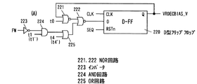
次に、図10に、本実施の形態における制御信号VRDECBIAS_Vの制御回路を示す。図5(B)に示される第1の実施の形態の同回路に比べて、インバータ223、AND回路224、OR回路225が追加されている。インバータ223に入力される信号FWは、フラッシュライトの条件により“H”レベルとなる信号である。この信号FWは、書き込み動作を指定するコマンド入力等によって、出力が決定される。書き込み動作が開始されると、信号FWに関わらず、まず時刻t0で制御信号VRDECBIAS_Vが“H”レベルになる。その後、信号FWが“L”レベルの場合には、例えば、通常のページ書き込み動作の場合には、AND回路224に入力される時刻t1の信号によって、制御信号VRDECBIAS_Vが“L”レベルになる。この場合、制御信号VRDECBIAS_Vは、図4のような波形となる。一方で、信号FWが“H”レベルの場合には、OR回路225に入力される時刻t4の信号によって、制御信号VRDECBIAS_Vが“L”レベルになる。この場合、制御信号VRDECBIAS_Vは、図8のような波形となる。図10において、時刻に対応する信号t 1やt4は、フラッシュライト時には、異なる時刻t1’、t4’になる。
【0045】
このようにして、通常の書き込み動作においては、ノードVRDECをフローティング制御し、フラッシュライト時には、ノードVRDECをフローティングにしない制御を行うことができる。
【0046】
なお、この第2の実施の形態では、全ブロック、全メモリセル選択時の書き込み動作時に制御信号VRDECをフローティングにしないと説明したが、ノードVRDECをフローティングにしない条件は、これに限らず、ブロック内の所定数のワード線を同時選択した場合や、ブロック内の所定数のワード線を同時選択し、かつ、所定数の複数のブロックを同時選択した場合にも適用してよい。
【0047】
本実施の形態によれば、第1の実施の形態同様の効果を得た上で、フラッシュライト時の素子破壊を防止できる。すなわち、制御信号VRDECの電位を通常のプログラム時には、フローティング状態に設定し、フラッシュライト時には、プログラム中、所定の電位を印加し続けるように書き込み動作中の制御を切り替えて、所望の書き込み電圧をワード線に与え、かつ、素子の破壊を防止した半導体記憶装置を提供できる。
【0048】
【発明の効果】
本発明によれば、所望の書き込み電圧をワード線に与えることが可能な半導体記憶装置を提供できる。
【図面の簡単な説明】
【図1】 本発明の第1の実施の形態の半導体記憶装置を示すブロック図。
【図2】 本発明の第1の実施の形態の半導体記憶装置のメモリセルアレイを示す回路図。
【図3】 本発明の第1の実施の形態の半導体記憶装置のVRDECドライバ回路の構成を示す回路図。
【図4】 本発明の第1の実施の形態の半導体記憶装置の書き込み動作を示すタイミングチャート。
【図5】 (A)は、本発明の第1の実施の形態の半導体記憶装置のVRDEC_V制御回路の構成を示す論理回路図であり、(B)は、本発明の第1の実施の形態の半導体記憶装置のVRDECBIAS_V制御回路の構成を示す論理回路図である。
【図6】 本発明の第1の実施の形態の半導体記憶装置の時間に対する書き込み・読み出し電圧の変化を示す電圧変化図。
【図7】 本発明の第1の実施の形態の半導体記憶装置のメモリセルアレイへ通常書き込みを行う場合の電圧変化を表す回路図。
【図8】 本発明の第2の実施の形態の半導体記憶装置のフラッシュライト時の書き込み動作を示すタイミングチャート。
【図9】 本発明の第2の実施の形態の半導体記憶装置のメモリセルアレイへFラッシュライトを行う場合の電圧変化を表す回路図。
【図10】 本発明の第2の実施の形態の半導体記憶装置のVRDECBIAS_V制御回路を示す論理回路図。
【図11】 従来の半導体記憶装置を示すブロック図。
【図12】 従来のVRDECドライバを示す回路図。
【図13】 従来の半導体記憶装置の書き込み動作を示すタイミングチャート。
【図14】 従来の半導体記憶装置のレベルシフタの構成を示す回路図。
【図15】 従来の半導体記憶装置のレベルシフタの回路中のトランジスタの閾値と電流量の関係を示す電圧・電流特性図。
【符号の説明】
1 デコーダ
2、21 レベルシフタ
3 転送トランジスタ
5 SGSドライバ
6 CGドライバ
7 SGDドライバ
10 ロウデコーダ
11 制御回路
12 コマンドレジスタ
20 VRDECドライバ
22、24、90 DタイプNMOSトランジスタ
23、26、223 インバータ
25 電圧降下トランジスタ
27 NAND回路
30 VPP pump回路
40 VPASS pump回路
50 センスアンプ
91 PMOSトランジスタ
92 NMOSトランジスタ
100 ブロック
101 NAND型セル
200、210、220 D型フリップフロップ
201、202、211、212、221、222 NOR回路
224 AND回路
225 OR回路
MC0、MC1、・・・、MC15、MC メモリセルトランジスタ
ST1、ST2 選択トランジスタ
WL0、WL1、・・・、WL15 ワード線[0001]
BACKGROUND OF THE INVENTION
The present invention relates to an electrically rewritable semiconductor memory device, and more particularly to a semiconductor memory device in which a write control operation is performed.
[0002]
[Prior art]
As shown in FIG. 11, the configuration of a conventional semiconductor memory device includes a
[0003]
For example, a NAND flash memory cell is provided in the memory area. In FIG. 11, the vertical direction is the row direction and the horizontal direction is the column direction. The number of memory cells in the row and column directions is appropriately set according to the memory capacity.
[0004]
FIG. 13 shows potentials of several nodes of this semiconductor memory device as write operation waveforms. At time t0, the block is selected by the input address, and the
[0005]
When the write voltage VPGM and the write intermediate voltage VPASS are transferred from the voltage supply
[0006]
By the way, in the circuit configuration as shown in FIG. 11, the voltage VPGMH for transferring the write voltage VPGM by the transfer transistor 3 is parasitic on the path for transferring VPGM when the supply of the voltage VPGM is started at the time t1. The voltage VPGMH also goes down depending on the capacity and word line capacity. This tendency increases when the capacity of the
[0007]
Next, FIG. 14 shows a circuit configuration of the
A D-
[0008]
Here, when a block decoder including the level shifter is selected, the
[0009]
[Problems to be solved by the invention]
The conventional semiconductor memory device as described above has the following problems. Due to the problem of the operation margin of the level shifter, there may occur a case where the voltage of VPGMH cannot be completely transferred to the gate Transfer G of the transfer transistor 3 as in the waveform of C1 in FIG.
[0010]
Here, the relationship between the threshold value of the NMOS D-type transistor in the
[0011]
At this time, in terms of DC operation, after the level shifter is charged to a voltage like the C1 waveform indicated by the broken line in FIG. 13, the gate Transfer G of the transfer transistor 3 is in a floating state. Since the write voltage VPGM (20V) is transferred to the word line at the timing t1, when the potential of the voltage VPGMH charged to the control signal VRDEC decreases as described above, the potential of the gate Transfer G of the transfer transistor 3 decreases accordingly. Until the time tf, the gate Transfer G of the transfer transistor 3 is biased in a DC manner. Since the gate Transfer G of the transfer transistor 3 becomes floating after the time tf, the potential of the gate Transfer G of the transfer transistor 3 becomes the coupling effect even after the time tf due to the contribution of the write voltage VPGM and the write intermediate voltage VPASS during the rise. Slightly rises, but looks like waveform C2. The potential of waveform C2 is higher than the potential of waveform C1, but if it has not increased to 20 V + Vtn which is the potential of VPGMH, the voltage transferred to the selected word line is a low voltage determined by waveform C2, VPGM (20V) is not transferred. That is, the write voltage VPGM cannot be transferred completely.
[0012]
In a normal state, the potential waveform of the transfer gate is represented by A and becomes the potential of the waveform VPGMH. Since the potential VPGMH is a voltage obtained by adding the threshold value of the transfer gate to the
[0013]
In such a case, there has been a case where a desired write voltage cannot be applied to the word line of the memory cell due to an operation margin problem of the level shifter.
[0014]
An object of the present invention is to solve the above-described problems of the prior art. In particular, an object of the present invention is to provide a voltage transfer control method that is less susceptible to a circuit operation margin of a row decoder.
[0015]
[Means for Solving the Problems]
In order to solve the above problems, the present invention is characterized in that a memory cell array in which electrically rewritable memory cells are arranged in a matrix and a plurality of word lines for selecting word lines of the memory cells in accordance with an address input A selection means; a word line voltage supply circuit for supplying a first voltage to the word line via the word line selection means; and a first voltage output from the word line voltage supply circuit for transferring to the word line. In the operation of supplying the second voltage to the word line selection means and supplying the first voltage from the word line voltage supply circuit to the word line after the second voltage is supplied to the word line selection means. A transfer voltage supply circuit for stopping the supply of the second voltage before supplying the first voltage, a booster circuit for generating the second voltage, and a voltage drop from the second voltage to reduce the first voltage. Occurrence And a semiconductor memory device having a voltage drop means that.
[0016]
DETAILED DESCRIPTION OF THE INVENTION
(First embodiment)
As a semiconductor memory device of this embodiment, a NAND flash memory will be described as one of electrically rewritable nonvolatile memories. FIG. 1 shows a connection relationship between a part of the memory cell array, a row decoder, and a sense amplifier. The
[0017]
The bit lines BL0 to BLi connected to each NAND cell are connected to the
[0018]
Here, a write operation to a NAND type memory cell will be described with reference to FIG. When writing is performed to shift the memory cell threshold, the bit line BL is set to 0V.
Here, when a Vdd potential of 2.5 V is applied to the gate of the selection transistor ST2, the selection gate ST2 is turned on, and 10 V is applied to each gate of the non-write memory cells MC0, MC2 to MC15, and writing is performed. 20 V is applied to the gate of the memory cell MC1 to be performed, and each memory cell is turned on. The CELSRC signal line is given a potential of 1 to 2 V, but 0 V is given to the gate of the selection transistor ST1, and the selection transistor ST1 is in a cut-off state. Since a potential of 0V is transferred from the bit line to the memory cell MC1 via the selection gate ST2 and the memory cells MC2 to MC15, a potential difference of 20V is generated between the gate and the channel in the memory cell MC1. Therefore, electrons are injected into the floating gate and writing is performed. Since an intermediate potential of 10 V is applied to the gates of the memory cells MC0 and MC2 to MC15, writing to these memory cells is not performed.
[0019]
On the other hand, when writing without threshold shift, the bit line BL is set to the Vdd potential (2.5 V). In this case, the selection transistor ST2 cuts off after transferring the potential of 2.5V-Vt (Vt is the threshold of the selection transistor ST2) into the NAND cell. Therefore, if an intermediate potential of 10V is applied to the gates of the memory cells MC0, MC2 to MC15 and 20V is applied to the gate of the memory cell MC1, all channel potentials in the floating NAND cell are coupled to 2.5V by coupling. It rises to a potential higher than −Vt. As a result, a potential difference that does not generate an FN (Fowler-Nordheim) tunnel current is applied between the gate and the channel of the selected memory cell MC1, and a threshold shift does not occur.
[0020]
The
The
[0021]
The
[0022]
The output voltage VPGMH of the
[0023]
These
[0024]
Here, the circuit of the
[0025]
Here, in the circuit of FIG. 3, the AND logic output of the control signals VRDEC_V and VRDECBIAS_V is input to the
[0026]
If the same potential as the voltage VRDEC can be transferred to the transfer transistor gate Transfer G by the time t1, as in the waveform E, the transfer transistor 3 is affected by the coupling effect from the CG line and the word line. The potential of the gate Transfer G is substantially the same as that of the floating signal VRDEC. At this time, since the parasitic capacitance of the floating signal VRDEC is larger than the capacitance of the gate Transfer G of the transfer transistor 3 in the selected block, the floating capacitance is maintained at a substantially constant floating potential after the floating state at time t1. In FIG. 4, 20V + Vtn is the potential of Transfer G, and 20V (B) is the potential of the word line. Strictly speaking, the potential of Transfer G is determined by the transistor characteristics in the
[0027]
At time t2, the word line potential 20V starts to drop. This time t2 is, for example, about 20 μsec. Next, at time t3, the unselected word line potential starts to drop from 10V. This time t3 is, for example, about 22 μsec. Next, at time t4, the gate voltage starts to drop from 20V + Vtn. This time t4 is, for example, about 24 μsec. The selected bit line BL is at the Vdd level when “1” is programmed, and at the Vss level when “0” is programmed.
[0028]
The selection gates SGD and SGS are both Vdd and 0V at time t0, and are 0V at time t4. FIG. 5A illustrates an example of a circuit that controls the signal VRDEC_V. This circuit includes a D-
[0029]
FIG. 5B illustrates an example of a circuit that controls the signal VRDECBIAS_V. The configuration of this circuit is the same as that of the VRDEC_V control circuit shown in FIG. As shown in FIG. 4, the signal t1 is input to the NOR
[0030]
In the above description, the write voltage has been described as 20 V. However, in the actual write operation of the NAND flash memory, the operation of applying the write voltage and the verify read operation are repeated as shown in FIG. The write voltage is gradually increased every time.
[0031]
At the time of the first writing, the lowest writing voltage is given as shown by (1). Thereafter, a verify operation is performed. If the desired data is not correctly written after the first verify, a voltage higher by ΔVpgm than the first write voltage is applied, and the second write operation is performed. Next, the second verify operation is performed. Thereafter, when desired data is not correctly written, a write voltage higher by ΔVpgm than the second write voltage is further applied, and the third write operation is performed. Next, a third verify operation is performed. In this way, in the normal write operation, the write operation and the verify operation are repeated about five times, and the write voltage increases each time. In order to cope with variations in the write characteristics of the memory cells and deterioration of the write characteristics, it is effective as a control method to increase the write voltage in this way, so that the desired write voltage can be transferred to the word line in a wide range. Is essential.
[0032]
Here, when the threshold value of the transistor in the level shifter of the row decoder changes greatly for some reason and the desired voltage is not transferred to the transfer gate Transfer G, the desired write voltage is applied to the word line (gate) of the memory cell to be written. It will not be given. Such a margin can be prevented by adopting the configuration of this embodiment.
[0033]
Next, FIG. 7 shows the coupling effect in the row decoder when normal writing is performed to the memory cell array. Here, 20 V is applied to one word line WL0 in order to write to the selected memory cell. An intermediate potential of 10V is applied to the other word lines WL1 to WL15. Here, due to the coupling capacitance between the signal line of the gate Transfer G of the transfer transistor 3 and each CG line and each word line, the voltage of Transfer G can be pushed up to some extent when a voltage is applied to these word lines. . The present embodiment makes effective use of this effect.
[0034]
In the semiconductor memory device of this embodiment, in the write operation of the NAND flash memory, the row decoder is controlled to be floating at a predetermined timing by controlling the path for supplying the transfer voltage for transferring the write voltage to the word line. Writing can be performed even when the transfer capability of the provided level shifter or local pump is insufficient.
[0035]
Therefore, even when the device characteristics are deteriorated, the operation margin can be widened as an operable semiconductor memory device. As described above, in this embodiment, a desired write voltage can be applied to the word line by switching the potential of the control signal VRDEC from the supply state of the signal VPGMH to the floating state at the time of writing.
[0036]
(Second Embodiment)
The semiconductor memory device according to the present embodiment has the following features in addition to the semiconductor memory device according to the first embodiment. FIG. 8 shows waveforms during a write operation to all memory cells in all blocks in the semiconductor memory device. In the first embodiment, it has been described that the control signal VRDEC is controlled to be floating at the timing when the write voltage is applied to the word line. However, in a write operation (Flash Write) for all blocks and all memory cells, it is not preferable to make the control signal VRDEC floating. The semiconductor memory device of this embodiment prevents this undesirable operation.
[0037]
First, a case where the control signal VRDEC is floated in the flash write operation will be described. When the write operation of the flash light is started at time t0, first, the control signal VRDEC is charged to the potential of VPGMH. At this time, since all the blocks are in the selected state, the load capacity of VPGGM is large, but it is assumed that it is charged to the potential of VPGMH until time t1 ′ as shown in FIG. When the control signal VRDEC is biased to the VPGMH potential at the time t1 'and the control to shift to the floating state is performed, the VPGM potential is charged to all word lines in the chip of the semiconductor memory device from the time t1'. Since the load of the potential VPGM increases remarkably, the output voltage itself of the
[0038]
As the voltages of all the word lines rise, the gate voltage Transfer G of the transfer transistor 3 rises due to coupling in the CG line, the word line, and all the row decoders as described above. At this time, the magnitude of the potential increase of the gate voltage Transfer G of the transfer transistor 3 due to the coupling becomes very large because all the word lines in the NAND cell have the amplitude of the potential VPGM. Here, when the control signal VRDEC is in a floating state, the charges boosted by the gate voltage Transfer G of the transfer transistors 3 of all the blocks flow in. Therefore, the potential of the wiring of the control signal VRDEC also increases greatly. End up.
[0039]
In the first embodiment, since the charge boosted by the gate voltage Transfer G of the transfer transistor 3 of one block only flows into the control signal VRDEC, the potential increase of the control signal VRDEC is suppressed to a small level. Accordingly, in the case where the gate voltage Transfer G of the transfer transistor 3 is charged to the same potential VPGMH as the control signal VRDEC in all the row decoders until time t1 ′, the waveform G is obtained, and the gate of the transfer transistor 3 is The potential of the voltage Transfer G and the potential of the control signal VRDEC become very high, and a potential exceeding the element breakdown voltage is applied to the elements of the
[0040]
If the transfer G charge level at time t1 'is low due to the operation margin of the level shifter of the row decoder, the waveform H is lower than the waveform G, but the waveform G or waveform H Since it is an operation margin problem determined by the capability of the level shifter, it is difficult to control it separately. Thus, after time t1 ′, the potential of the selected word line rises with a slow rise. Here, the potential difference between the waveform G and the waveform H is, for example, about 1V to 2V.
[0041]
Therefore, in order to avoid the element breakdown due to excessive voltage rise as in the waveform G, writing is performed while the control signal VRDECBIAS_V is kept at “H” level at the time of flash write. In other words, VPGGMH is continuously supplied to the control signal VRDEC without floating the control signal VRDEC at time t1 ′. In this case, measures against the operation margin problem of the level shifter of the row decoder are not taken, but it is possible to cope with preventing element destruction.
[0042]
The control signal VRDECBIAS_V is controlled by the condition of flash write so as not to make the control signal VRDEC floating during flash write. That is, when all blocks are selected, or when all blocks are selected and all pages in the NAND are selected, the control signal VRDECBIAS_V is maintained at the “H” level.
[0043]
Next, FIG. 9 is a circuit diagram showing a voltage change when performing flash write to the memory cell array. Here, in order to perform writing to all the memory cells, 20 V is applied to all the word lines. Here, coupling occurs between the Transfer G signal line and each word line, but the effect of 20 V, which is the potential of the 16 word lines, is large, so the coupling effect is larger than that during normal writing. Become.
[0044]
Next, FIG. 10 shows a control circuit for the control signal VRDECBIAS_V in this embodiment. Compared to the circuit of the first embodiment shown in FIG. 5B, an
[0045]
In this manner, in the normal write operation, the node VRDEC can be controlled to be floating, and control can be performed so that the node VRDEC is not floating at the time of flash write.
[0046]
In the second embodiment, it has been described that the control signal VRDEC is not floated during the write operation when all blocks and all memory cells are selected. However, the condition that the node VRDEC is not floated is not limited to this. The present invention may also be applied to a case where a predetermined number of word lines are simultaneously selected, or a case where a predetermined number of word lines within a block are simultaneously selected and a predetermined number of blocks are simultaneously selected.
[0047]
According to the present embodiment, it is possible to prevent element destruction during flash writing while obtaining the same effects as those of the first embodiment. That is, the potential of the control signal VRDEC is set to a floating state during normal programming, and during flash programming, the control during the writing operation is switched so that a predetermined potential is continuously applied during programming, and a desired writing voltage is set to the word. It is possible to provide a semiconductor memory device that is applied to a line and prevents destruction of elements.
[0048]
【The invention's effect】
According to the present invention, it is possible to provide a semiconductor memory device capable of applying a desired write voltage to a word line.
[Brief description of the drawings]
FIG. 1 is a block diagram showing a semiconductor memory device according to a first embodiment of the present invention.
FIG. 2 is a circuit diagram showing a memory cell array of the semiconductor memory device according to the first embodiment of the present invention.
FIG. 3 is a circuit diagram showing a configuration of a VRDEC driver circuit of the semiconductor memory device according to the first embodiment of the present invention.
FIG. 4 is a timing chart showing a write operation of the semiconductor memory device according to the first embodiment of the present invention.
5A is a logic circuit diagram showing a configuration of a VRDEC_V control circuit of the semiconductor memory device according to the first embodiment of the present invention, and FIG. 5B is a first embodiment of the present invention. 2 is a logic circuit diagram showing a configuration of a VRDECBIAS_V control circuit of the semiconductor memory device of FIG.
FIG. 6 is a voltage change diagram showing a change in write / read voltage with respect to time of the semiconductor memory device according to the first embodiment of the present invention;
FIG. 7 is a circuit diagram showing a voltage change when normal writing is performed in the memory cell array of the semiconductor memory device according to the first embodiment of the present invention;
FIG. 8 is a timing chart showing a write operation during flash write in the semiconductor memory device according to the second embodiment of the present invention.
FIG. 9 is a circuit diagram showing a voltage change when F rush write is performed on the memory cell array of the semiconductor memory device according to the second embodiment of the present invention;
FIG. 10 is a logic circuit diagram showing a VRDECBIAS_V control circuit of a semiconductor memory device according to a second embodiment of the present invention.
FIG. 11 is a block diagram showing a conventional semiconductor memory device.
FIG. 12 is a circuit diagram showing a conventional VRDEC driver.
FIG. 13 is a timing chart showing a write operation of a conventional semiconductor memory device.
FIG. 14 is a circuit diagram showing a configuration of a level shifter of a conventional semiconductor memory device.
FIG. 15 is a voltage / current characteristic diagram showing the relationship between the threshold value of a transistor and the amount of current in a level shifter circuit of a conventional semiconductor memory device.
[Explanation of symbols]
1 Decoder
2, 21 level shifter
3 Transfer transistor
5 SGS driver
6 CG driver
7 SGD driver
10 Row decoder
11 Control circuit
12 Command register
20 VRDEC drivers
22, 24, 90 D-type NMOS transistor
23, 26, 223 inverter
25 Voltage drop transistor
27 NAND circuit
30 VPP pump circuit
40 VPASS pump circuit
50 sense amplifiers
91 PMOS transistor
92 NMOS transistor
100 blocks
101 NAND cell
200, 210, 220 D-type flip-flop
201, 202, 211, 212, 221, 222 NOR circuit
224 AND circuit
225 OR circuit
MC0, MC1, ..., MC15, MC Memory cell transistor
ST1, ST2 selection transistor
WL0, WL1, ..., WL15 Word line
Claims (7)
アドレス入力に応じて前記メモリセルのワード線を選択する複数のワード線選択手段と、
このワード線選択手段を介して前記ワード線に第一の電圧を供給するワード線電圧供給回路と、
このワード線電圧供給回路から出力される前記第一の電圧を前記ワード線に転送するために前記ワード線選択手段に第二の電圧を供給し、この第二の電圧を前記ワード線選択手段に供給した後に前記ワード線電圧供給回路から前記ワード線に前記第一の電圧を供給する動作において、前記ワード線に前記第一の電圧を供給する前に前記第二の電圧の供給を停止する転送電圧供給回路と、
前記第二の電圧を発生する昇圧回路と、
前記第二の電圧から電圧降下させて前記第一の電圧を発生する電圧降下手段とを有することを特徴とする半導体記憶装置。A memory cell array in which electrically rewritable memory cells are arranged in a matrix;
A plurality of word line selection means for selecting a word line of the memory cell in response to an address input;
A word line voltage supply circuit for supplying a first voltage to the word line via the word line selection means;
In order to transfer the first voltage output from the word line voltage supply circuit to the word line, a second voltage is supplied to the word line selection means, and the second voltage is supplied to the word line selection means. In the operation of supplying the first voltage from the word line voltage supply circuit to the word line after the supply, the transfer for stopping the supply of the second voltage before supplying the first voltage to the word line A voltage supply circuit;
A booster circuit for generating the second voltage;
And a voltage drop means for generating the first voltage by dropping the voltage from the second voltage.
Priority Applications (4)
| Application Number | Priority Date | Filing Date | Title |
|---|---|---|---|
| JP2002006847A JP3702229B2 (en) | 2002-01-16 | 2002-01-16 | Semiconductor memory device |
| US10/345,030 US6807099B2 (en) | 2002-01-16 | 2003-01-14 | Semiconductor memory device |
| KR10-2003-0002635A KR100482232B1 (en) | 2002-01-16 | 2003-01-15 | Semiconductor memory device |
| US10/935,868 US6891757B2 (en) | 2002-01-16 | 2004-09-08 | Semiconductor memory device |
Applications Claiming Priority (1)
| Application Number | Priority Date | Filing Date | Title |
|---|---|---|---|
| JP2002006847A JP3702229B2 (en) | 2002-01-16 | 2002-01-16 | Semiconductor memory device |
Publications (2)
| Publication Number | Publication Date |
|---|---|
| JP2003208793A JP2003208793A (en) | 2003-07-25 |
| JP3702229B2 true JP3702229B2 (en) | 2005-10-05 |
Family
ID=19191280
Family Applications (1)
| Application Number | Title | Priority Date | Filing Date |
|---|---|---|---|
| JP2002006847A Expired - Fee Related JP3702229B2 (en) | 2002-01-16 | 2002-01-16 | Semiconductor memory device |
Country Status (3)
| Country | Link |
|---|---|
| US (2) | US6807099B2 (en) |
| JP (1) | JP3702229B2 (en) |
| KR (1) | KR100482232B1 (en) |
Cited By (1)
| Publication number | Priority date | Publication date | Assignee | Title |
|---|---|---|---|---|
| US8902670B2 (en) | 2012-08-31 | 2014-12-02 | Kabushiki Kaisha Toshiba | Semiconductor memory device |
Families Citing this family (21)
| Publication number | Priority date | Publication date | Assignee | Title |
|---|---|---|---|---|
| JP4157065B2 (en) | 2004-03-29 | 2008-09-24 | 株式会社東芝 | Semiconductor memory device |
| JP4256305B2 (en) * | 2004-06-09 | 2009-04-22 | 株式会社東芝 | Semiconductor memory device |
| KR100624302B1 (en) * | 2004-10-07 | 2006-09-19 | 주식회사 하이닉스반도체 | Row Decoder Circuit of NAND Flash Memory and Operation Voltage Supply Method Using Same |
| US7173859B2 (en) * | 2004-11-16 | 2007-02-06 | Sandisk Corporation | Faster programming of higher level states in multi-level cell flash memory |
| JP2006179065A (en) * | 2004-12-21 | 2006-07-06 | Toshiba Corp | Semiconductor memory device and memory card |
| KR100648289B1 (en) * | 2005-07-25 | 2006-11-23 | 삼성전자주식회사 | Flash memory device and its programming method which can improve the program speed |
| KR100655430B1 (en) * | 2005-11-17 | 2006-12-08 | 삼성전자주식회사 | Flash memory device and its word line enable method |
| KR100704039B1 (en) | 2006-01-20 | 2007-04-04 | 삼성전자주식회사 | Semiconductor memory device in which the decoded signal is bused in the word line direction |
| US7710786B2 (en) * | 2006-08-28 | 2010-05-04 | Micron Technology, Inc. | NAND flash memory programming |
| US7593259B2 (en) * | 2006-09-13 | 2009-09-22 | Mosaid Technologies Incorporated | Flash multi-level threshold distribution scheme |
| US7474561B2 (en) * | 2006-10-10 | 2009-01-06 | Sandisk Corporation | Variable program voltage increment values in non-volatile memory program operations |
| US7450426B2 (en) * | 2006-10-10 | 2008-11-11 | Sandisk Corporation | Systems utilizing variable program voltage increment values in non-volatile memory program operations |
| KR101354608B1 (en) * | 2007-09-21 | 2014-01-22 | 삼성전자주식회사 | Flash memory device and program method thereof |
| JP2009266351A (en) * | 2008-04-28 | 2009-11-12 | Toshiba Corp | Semiconductor memory device and method of controlling the same |
| JP2010157277A (en) * | 2008-12-26 | 2010-07-15 | Toshiba Corp | Nonvolatile semiconductor memory device |
| JP5259666B2 (en) * | 2010-09-22 | 2013-08-07 | 株式会社東芝 | Nonvolatile semiconductor memory device |
| JP2014179148A (en) | 2013-03-15 | 2014-09-25 | Toshiba Corp | Nonvolatile semiconductor memory device |
| JP2017228325A (en) * | 2016-06-20 | 2017-12-28 | ウィンボンド エレクトロニクス コーポレーション | Nonvolatile semiconductor memory device |
| US10388382B2 (en) * | 2017-08-31 | 2019-08-20 | Micron Technology, Inc. | Methods and apparatus for programming memory |
| US10867684B1 (en) * | 2019-08-29 | 2020-12-15 | Micron Technology, Inc. | Driving access lines to target voltage levels |
| JP2023095471A (en) * | 2021-12-24 | 2023-07-06 | キオクシア株式会社 | semiconductor storage device |
Family Cites Families (4)
| Publication number | Priority date | Publication date | Assignee | Title |
|---|---|---|---|---|
| JP3362661B2 (en) * | 1998-03-11 | 2003-01-07 | 日本電気株式会社 | Nonvolatile semiconductor memory device |
| US5991201A (en) * | 1998-04-27 | 1999-11-23 | Motorola Inc. | Non-volatile memory with over-program protection and method therefor |
| JP3822410B2 (en) | 1999-01-29 | 2006-09-20 | 株式会社東芝 | Semiconductor integrated circuit |
| JP4157269B2 (en) | 2000-06-09 | 2008-10-01 | 株式会社東芝 | Semiconductor memory device |
-
2002
- 2002-01-16 JP JP2002006847A patent/JP3702229B2/en not_active Expired - Fee Related
-
2003
- 2003-01-14 US US10/345,030 patent/US6807099B2/en not_active Expired - Fee Related
- 2003-01-15 KR KR10-2003-0002635A patent/KR100482232B1/en not_active Expired - Fee Related
-
2004
- 2004-09-08 US US10/935,868 patent/US6891757B2/en not_active Expired - Fee Related
Cited By (1)
| Publication number | Priority date | Publication date | Assignee | Title |
|---|---|---|---|---|
| US8902670B2 (en) | 2012-08-31 | 2014-12-02 | Kabushiki Kaisha Toshiba | Semiconductor memory device |
Also Published As
| Publication number | Publication date |
|---|---|
| KR100482232B1 (en) | 2005-04-14 |
| KR20030062275A (en) | 2003-07-23 |
| US20050030812A1 (en) | 2005-02-10 |
| US6891757B2 (en) | 2005-05-10 |
| JP2003208793A (en) | 2003-07-25 |
| US20030133326A1 (en) | 2003-07-17 |
| US6807099B2 (en) | 2004-10-19 |
Similar Documents
| Publication | Publication Date | Title |
|---|---|---|
| JP3702229B2 (en) | Semiconductor memory device | |
| KR100454116B1 (en) | Bit line setup and discharge circuit for programming non-volatile memory | |
| US8537617B2 (en) | Source side asymmetrical precharge programming scheme | |
| JP4856138B2 (en) | Nonvolatile semiconductor memory device | |
| KR100784862B1 (en) | Flash memory device containing dummy cells | |
| JP4097017B2 (en) | Nonvolatile semiconductor memory device and program method thereof. | |
| JP5992983B2 (en) | Nonvolatile semiconductor memory device | |
| JP2008140488A (en) | Semiconductor memory device | |
| JP2008084471A (en) | Semiconductor memory device | |
| JP2008146771A (en) | Semiconductor memory device | |
| US7161837B2 (en) | Row decoder circuit of NAND flash memory and method of supplying an operating voltage using the same | |
| US9870828B2 (en) | Non-volatile semiconductor memory and erasing method thereof | |
| JP2013200932A (en) | Non-volatile semiconductor memory device | |
| JP2009272026A (en) | Nonvolatile semiconductor memory device | |
| JP2019096369A (en) | Semiconductor storage device | |
| US8339866B2 (en) | Semiconductor memory device | |
| KR20090044762A (en) | Flash memory device | |
| JP4846814B2 (en) | Nonvolatile semiconductor memory device | |
| JP2007305204A (en) | Nonvolatile semiconductor memory device | |
| JP2008300019A (en) | Nonvolatile semiconductor memory device | |
| US10014064B2 (en) | Non-volatile semiconductor storage device | |
| JP2006331476A (en) | Nonvolatile semiconductor memory device | |
| KR20100010673A (en) | Nonvolatile memory device, reading and driving method thereof | |
| JP4615297B2 (en) | Semiconductor memory device | |
| JP2013198308A (en) | Voltage generating circuit |
Legal Events
| Date | Code | Title | Description |
|---|---|---|---|
| RD02 | Notification of acceptance of power of attorney |
Free format text: JAPANESE INTERMEDIATE CODE: A7422 Effective date: 20050414 |
|
| RD04 | Notification of resignation of power of attorney |
Free format text: JAPANESE INTERMEDIATE CODE: A7424 Effective date: 20050606 |
|
| A977 | Report on retrieval |
Free format text: JAPANESE INTERMEDIATE CODE: A971007 Effective date: 20050704 |
|
| TRDD | Decision of grant or rejection written | ||
| A01 | Written decision to grant a patent or to grant a registration (utility model) |
Free format text: JAPANESE INTERMEDIATE CODE: A01 Effective date: 20050712 |
|
| A61 | First payment of annual fees (during grant procedure) |
Free format text: JAPANESE INTERMEDIATE CODE: A61 Effective date: 20050715 |
|
| FPAY | Renewal fee payment (event date is renewal date of database) |
Free format text: PAYMENT UNTIL: 20090722 Year of fee payment: 4 |
|
| FPAY | Renewal fee payment (event date is renewal date of database) |
Free format text: PAYMENT UNTIL: 20090722 Year of fee payment: 4 |
|
| FPAY | Renewal fee payment (event date is renewal date of database) |
Free format text: PAYMENT UNTIL: 20100722 Year of fee payment: 5 |
|
| FPAY | Renewal fee payment (event date is renewal date of database) |
Free format text: PAYMENT UNTIL: 20110722 Year of fee payment: 6 |
|
| FPAY | Renewal fee payment (event date is renewal date of database) |
Free format text: PAYMENT UNTIL: 20120722 Year of fee payment: 7 |
|
| FPAY | Renewal fee payment (event date is renewal date of database) |
Free format text: PAYMENT UNTIL: 20130722 Year of fee payment: 8 |
|
| LAPS | Cancellation because of no payment of annual fees |