JP3678120B2 - Polarized light irradiation device - Google Patents
Polarized light irradiation device Download PDFInfo
- Publication number
- JP3678120B2 JP3678120B2 JP2000169631A JP2000169631A JP3678120B2 JP 3678120 B2 JP3678120 B2 JP 3678120B2 JP 2000169631 A JP2000169631 A JP 2000169631A JP 2000169631 A JP2000169631 A JP 2000169631A JP 3678120 B2 JP3678120 B2 JP 3678120B2
- Authority
- JP
- Japan
- Prior art keywords
- polarized light
- light
- mirror
- incident
- polarized
- Prior art date
- Legal status (The legal status is an assumption and is not a legal conclusion. Google has not performed a legal analysis and makes no representation as to the accuracy of the status listed.)
- Expired - Fee Related
Links
Images


Classifications
-
- G—PHYSICS
- G02—OPTICS
- G02F—OPTICAL DEVICES OR ARRANGEMENTS FOR THE CONTROL OF LIGHT BY MODIFICATION OF THE OPTICAL PROPERTIES OF THE MEDIA OF THE ELEMENTS INVOLVED THEREIN; NON-LINEAR OPTICS; FREQUENCY-CHANGING OF LIGHT; OPTICAL LOGIC ELEMENTS; OPTICAL ANALOGUE/DIGITAL CONVERTERS
- G02F1/00—Devices or arrangements for the control of the intensity, colour, phase, polarisation or direction of light arriving from an independent light source, e.g. switching, gating or modulating; Non-linear optics
- G02F1/01—Devices or arrangements for the control of the intensity, colour, phase, polarisation or direction of light arriving from an independent light source, e.g. switching, gating or modulating; Non-linear optics for the control of the intensity, phase, polarisation or colour
- G02F1/13—Devices or arrangements for the control of the intensity, colour, phase, polarisation or direction of light arriving from an independent light source, e.g. switching, gating or modulating; Non-linear optics for the control of the intensity, phase, polarisation or colour based on liquid crystals, e.g. single liquid crystal display cells
- G02F1/133—Constructional arrangements; Operation of liquid crystal cells; Circuit arrangements
- G02F1/1333—Constructional arrangements; Manufacturing methods
- G02F1/1337—Surface-induced orientation of the liquid crystal molecules, e.g. by alignment layers
-
- G—PHYSICS
- G02—OPTICS
- G02B—OPTICAL ELEMENTS, SYSTEMS OR APPARATUS
- G02B27/00—Optical systems or apparatus not provided for by any of the groups G02B1/00 - G02B26/00, G02B30/00
- G02B27/28—Optical systems or apparatus not provided for by any of the groups G02B1/00 - G02B26/00, G02B30/00 for polarising
-
- G—PHYSICS
- G02—OPTICS
- G02F—OPTICAL DEVICES OR ARRANGEMENTS FOR THE CONTROL OF LIGHT BY MODIFICATION OF THE OPTICAL PROPERTIES OF THE MEDIA OF THE ELEMENTS INVOLVED THEREIN; NON-LINEAR OPTICS; FREQUENCY-CHANGING OF LIGHT; OPTICAL LOGIC ELEMENTS; OPTICAL ANALOGUE/DIGITAL CONVERTERS
- G02F1/00—Devices or arrangements for the control of the intensity, colour, phase, polarisation or direction of light arriving from an independent light source, e.g. switching, gating or modulating; Non-linear optics
- G02F1/01—Devices or arrangements for the control of the intensity, colour, phase, polarisation or direction of light arriving from an independent light source, e.g. switching, gating or modulating; Non-linear optics for the control of the intensity, phase, polarisation or colour
- G02F1/13—Devices or arrangements for the control of the intensity, colour, phase, polarisation or direction of light arriving from an independent light source, e.g. switching, gating or modulating; Non-linear optics for the control of the intensity, phase, polarisation or colour based on liquid crystals, e.g. single liquid crystal display cells
- G02F1/133—Constructional arrangements; Operation of liquid crystal cells; Circuit arrangements
- G02F1/1333—Constructional arrangements; Manufacturing methods
- G02F1/1337—Surface-induced orientation of the liquid crystal molecules, e.g. by alignment layers
- G02F1/13378—Surface-induced orientation of the liquid crystal molecules, e.g. by alignment layers by treatment of the surface, e.g. embossing, rubbing or light irradiation
- G02F1/133788—Surface-induced orientation of the liquid crystal molecules, e.g. by alignment layers by treatment of the surface, e.g. embossing, rubbing or light irradiation by light irradiation, e.g. linearly polarised light photo-polymerisation
Landscapes
- Physics & Mathematics (AREA)
- General Physics & Mathematics (AREA)
- Optics & Photonics (AREA)
- Nonlinear Science (AREA)
- Liquid Crystal (AREA)
- Spectroscopy & Molecular Physics (AREA)
- Mathematical Physics (AREA)
- Chemical & Material Sciences (AREA)
- Crystallography & Structural Chemistry (AREA)
- Polarising Elements (AREA)
Description
【0001】
【発明の属する技術分野】
本発明は、液晶表示素子の配向膜に偏光光を照射して液晶を光配向させるための偏光光照射装置に関する。
【0002】
【従来の技術】
液晶表示素子は、透明基板の表面に形成した配向膜に、液晶を所望の方向に配向させる処理(配向処理) を施し、該透明基板を2枚、配向膜を内側にして、所定の間隔の隙間を保つように貼り合せ、該隙間に液晶を注入したものである。
配向膜の配向処理に関し、配向膜に所定の波長の偏光光を照射し露光処理することにより配向を行なう光配向と呼ばれる技術がある。
現在最も一般的に使用される、TN液晶と呼ばれる液晶表示素子は、液晶の配向方向が、2枚の透明基板の間で90°回転するように作られている。したがって、配向方向の異なる配向膜を形成した2枚の透明基板が必要となる。
また、液晶表示素子の1つの画素を2つもしくはそれ以上に分割し、分割した画素毎に液晶の配向方向を変えることにより、液晶表示素子の視野角を改善することが行われている。この方法は画素分割法、あるいはマルチドメイン法と呼ばれている。
光配向を上記画素分割法に適用する場合には、マスクを用いて、基板に形成された画素の分割した一つの部分に偏光光を照射し、次にマスクを交換し、分割した他の部分に、前記とは偏光方向を変えた光を照射する。
【0003】
上記のように、配向膜に偏光光を照射する光配向用偏光光照射装置においては、照射する偏光光の偏光方向を、任意の方向に変更できる装置が望ましい。本出願人は、先に特願平11−7618号において、該光照射装置内に設けた偏光素子を回転させることにより、基板を回転させることなく、基板に照射される偏光光の方向を変更できる、光照射装置を提案している。
【0004】
図11に偏光光の方向を変更できる光照射装置の構成例を示す。
図11において、ランプ1からの光は、楕円集光鏡2で集光され、第1平面鏡3によって光路が折り返され、偏光素子8に入射する。偏光素子8は例えば複数のガラス板を、光軸に対してブリュースタ角だけ傾けて配置したものであり、P偏光光は透過し、S偏光光の大部分が反射する。これにより、所望の消光比を有する偏光光が得られる。
偏光素子8から出射した偏光光(P偏光光) はインテグレータレンズ4に入射後、シャッタ5を介して第2平面鏡6によって折り返され、コリメータレンズ7に入射し、平行光とされた後、マスクMを介してワークW(基板)の配向膜に照射される。
偏光素子8は、光照射装置内において、偏光素子8に入射する光芒の中心を中心軸として、回転自在に設けられており、該偏光素子8を回転させることにより、配向膜に照射される偏光光の方向を、任意に変更・設定することができる。
なお、上記のように偏光素子8を回転させる代わりに、配向膜が形成されたワークWを載置するワークステージ(図示せず)を回転させるようにした装置もある。
【0005】
光照射装置においては、照射面積、照度分布、ワークに照射される光の平行度などの、光学設計上の問題から、必要とされる光路長が決まる。光照射装置を小型化し、かつ該光路長を確保するために、図11に示す第1平面鏡3、第2平面鏡6のようなミラーにより、光路を折り返す。
上記該平面鏡は石英板にアルミ等の金属を蒸着したミラーが用いられる。傷防止のためにミラー面にフツ化マグネシウム(MgF2 )、二酸化ケイ素(SiO2 )、酸化アルミニウム(Al2 O3 )などの保護膜が、通常、数十〜百数十nmの厚さで蒸着されている場合が多い。
【0006】
【発明が解決しようとする課題】
光配向膜を配向させるためには、所定の波長であって、所定の値以上の消光比を有する偏光光が必要である。これは配向膜の物性により決まる。
消光比とは光に含まれるP偏光成分とS偏光成分の割合である。光配向膜を配向させるためには、消光比10:1以上が望ましいとされている。また、波長は250nm〜350nmの範囲の紫外光を使用する場合が多い。
ところが、図11の装置において、偏光素子から、直線偏光に近い(消光比の良い、例えば20:1〜15:1)偏光光を出射しても、ワークに照射される偏光光の偏光方向を変えようとして偏光素子を回転させると、消光比が低下し( 例えば6:1)、所望の消光比が得られない場合が生じた。
例えば、ブリュースタ角に配置されたガラスを偏光素子とすると、該偏光素子から出射される偏光光(P偏光)は直線偏光である。一般に、直線偏光光をミラーにより反射すると、場合によって反射光は位相のずれにより楕円偏光になることが知られている。これが消光比の低下する原因である。
【0007】
楕円偏光になる理由については次に簡単に説明する。
図12は、偏光素子から直線偏光光が出射し、ミラーに入射角45°で入射し、反射している状態を示す図である。偏光素子から出射する偏光光は紙面に対し上下方向の電場を有している(偏光方向が紙面上下方向である) とする。
図12において、偏光素子から出射される偏光光の光軸と、偏光光の電場の方向とによって決まる平面を平面Aとする。一方、ミラーへの入射光(即ち偏光素子からの出射光)の光軸と、ミラーからの反射光の光軸とによって決まる平面を平面Bとする。図12は、平面Aと平面Bとが互いに平行な場合である。
ここで、偏光素子を、光軸を回転軸として回転させると、平面Aと平面Bとは互いに平行ではなくなり、偏光素子が図12の状態から90°傾いたところで、平面Aと平面Bとは互いに直交する関係となる。
ミラーの反射面において、ミラーに入射する光の、平面Bに平行な成分をP偏光成分、平面Bに垂直な成分をS偏光成分という。
【0008】
平面Aと平面Bとが平行または垂直の関係にある時は、ミラーに入射する偏光光の電場の方向(偏光方向)は、P偏光成分、またはS偏光成分しか有さない。ところが、平面Aと平面Bとが平行または垂直の関係にない場合、例えば、ミラーに入射する直線偏光光の電場の方向(偏光方向)が、図13に示すような場合、ミラーに入射する光は、P偏光成分とS偏光成分とを有することとなる。
一般に、光はミラーにより反射すると位相がずれ、その位相のずれ量は、P偏光成分とS偏光成分とでは異なることが知られている。ミラーに入射する偏光光が、P偏光成分、または、S偏光成分しか持たない場合(平面Aと平面Bとが平行または垂直の関係にある場合)は、反射による位相のずれが生じても、反射光はP偏光成分、または、S偏光成分しか持たないので、反射光は入射光の消光比と同じ直線偏光光となる。
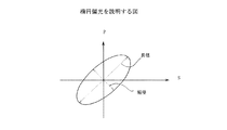
ところが、図13のように、偏光光が、P偏光成分とS偏光成分の両方を有するようにミラーに入射すると、上記したように、反射するP偏光成分の位相のずれ量と、S偏光成分位相のずれ量とが異なるために、P偏光成分とS偏光成分との間に位相差が生じ、反射光は図14に示すような楕円偏光になる(詳しくは、例えば「応用物理ハンドプック」応用物理学会編、丸善株式会社、平成2年3月30日発行、P20〜P22を参照)。
【0009】
即ち、理想的な直線偏光光(消光比が無限大)であっても、平面Aと平面Bとが平行または垂直の関係にない場合、ミラーから出射される光は楕円偏光となる。そして楕円偏光の消光比は、該楕円の長径に対する短径の比で表されるので、消光比は低下する。
したがって、図11の装置において、ワークWに照射される偏光光の偏光方向を変えようとして偏光素子8を回転させると、上記したように平面Aと平面Bとが平行または垂直の関係ではなくなり、第2平面鏡によって反射されると楕円偏光となり、ワークWに照射される偏光光の消光比が低下する。
本発明は上記従来技術の問題点を解決するためになされたものであって、本発明の目的は、偏光光を反射ミラーに入射し、該反射ミラーにより反射した偏光光を、光配向膜が形成されたワークに照射する光配向用偏光光照射装置において、反射ミラーに入射する偏光光の偏光方向を変化させても、ワークに照射される偏光光の消光比が、偏光素子から出射する偏光光の消光比に対して低下することのない偏光光照射装置を提供することである。
【0010】
【課題を解決するための手段】
ミラーに入射する直線偏光光の方位角をα、ミラーの反射によって生じるP偏光成分とS偏光成分の位相のずれ量の差をΔとすると、反射光の楕円偏光の長軸と短軸との長さの比で決まる楕円率角εとの間には、 sin2ε= sin2α× sinΔという関係が成り立つ(例えば、「光学的測定ハンドブツク」、朝倉書店、1981年7月25日発行P412参照)。
また、消光比=(1/ tanε)2 :1と表すことができる。これより、楕円率角εが小さいほど高い消光比が得られることがわかる。仮に、消光比が∞:1の直線偏光光をミラーに入射した時、ε=0の場合、反射光の消光比は∞:1となる。
一方、 sin2ε= sin2α× sinΔより、Δ=0であればε=0となり、この時の消光比は偏光光の偏光方向にかかわらず、消光比は∞:1となる。Δが大きくなるとεはαまで大きくなり得る。その場合、ミラーに偏光方向が45°傾いた偏光光が入射すると、反射光の消光比は1:1となる。
したがって、反射光の消光比を低下させないためには、理想的にはΔ=0またはΔ≒0になるように反射ミラーを構成すればよい。
上記式に基づき計算すると、消光比15:1の偏光光をミラーに入射した時、消光比10:1の反射光を得るためには、Δ≦±20°、消光比12:1の反射光を得るためには、Δ≦±15°、消光比13.5:1の反射光を得るためには、Δ≦±10°である必要がある。
【0011】
前記したように光配向膜を配向させるためには、消光比10:1以上が望ましい。そのためには上述したようにΔ≦±20°であることが必要であり、Δ≦±20°とするためには、次のような手段が考えられる。
P偏光成分とS偏光成分の位相のずれ量の差のΔは、ミラーに入射する光の波長、入射角度に依存する。さらにミラーの表面に保護膜を形成する場合には、該膜の種類、膜厚に依存する。したがって、以下に説明するように、ミラーへの偏光光の入射角、保護膜の厚さを適切に設定したり、P偏光成分とS偏光成分の位相のずれ量の差Δを打ち消すようなミラーの配置とすればよい。
(1)ミラー表面に膜を形成すると、ミラーに光が入射した時、膜表面で反射する光の位相に対して、膜を透過してミラー表面で反射する光の位相が、膜の光学的厚さに依存して遅れる。
この膜形成による位相のずれを利用すれば、反射光のP偏光成分とS偏光成分の位相のずれ量の差Δを小さくすることができる。
この位相のずれ量の差Δはミラーへの偏光光の入射角に依存する。また、光配向に用いられる波長は光配向膜の種類により決まる。したがって、光学的な設計により定まるミラーへの偏光光の入射角と、光配向膜を配向させるために要求される波長に応じて、ミラー表面に形成する保護膜の種類、及び膜の光学的厚さを選定すれば、Δ≦±20°とすることができ、消光比を10:1以上にすることができる。
(2)反射ミラーに入射する偏光光の入射角度を小さくすれば、反射光におけるP偏光成分とS偏光成分の位相のずれ量の差Δを小さくすることができる。
したがって、複数の反射ミラーを組み合わせ、各反射ミラーに入射する偏光光の入射角度が小さくなるようにすれば、Δ≦±20°とすることができ、消光比を10:1以上にすることができる。
(3)同じ材質の第1及び第2の反射ミラーを用い、第1の反射ミラーの入射光の光軸と反射光の光軸とにより決まる平面に対して、第2の反射ミラーの入射光の光軸と反射光の光軸とにより決まる平面が垂直になるように、かつ、第1の反射ミラーへの入射角度と第2の反射ミラーへの入射角度とが等しくなるように、上記第1と第2の反射ミラーを配置すれば、第1のミラーの反射によって生じた位相差を、第1のミラーの反射により打ち消すことができる。
したがって、少なくとも第1、第2の2枚の反射ミラーを用い、反射ミラーを上記配置とすることにより、P偏光成分とS偏光成分の位相のずれを無くすことができ、第2の反射ミラーで反射された偏光光を直線偏光とすることができる。
【0012】
【発明の実施の形態】
図1に本発明の第1の実施例の偏光光照射装置の構成を示す。図1において、前記図11に示したものと同一のものには同一の符号が付されており、本実施例においては、第2の平面鏡6の表面に誘電体膜(保護膜)11が形成されている。該誘電体膜の材質、膜厚は、第2の平面鏡6への偏光光の入射角と、ワークW上に形成された光配向膜を配向させるために要求されている波長に応じて、反射する偏光光のP偏光成分とS偏光成分の位相のずれ量の差Δが20°以下になるように選定されている。上記第2の平面鏡6は例えばアルミミラーであり、その表面に形成される誘電体膜11(以下、保護膜11という)としては、例えばフッ化マグネシウム(MgF2 )膜、あるいは二酸化ケイ素(SiO2 )膜を用いることができる。
【0013】
図1において、ランプ1からの光は、楕円集光鏡2で集光され、第1平面鏡3によって光路が折り返され、偏光素子8に入射する。偏光素子8は例えば前記したように、複数のガラス板を、光軸に対してブリュースタ角だけ傾けて配置したものであり、P偏光光は透過し、S偏光光の大部分を反射する。これにより、所望の消光比を有する偏光光が得られる。
偏光素子8から出射した偏光光(P偏光光) はインテグレータレンズ4に入射後、シャッタ5を介して、表面に上記保護膜11が形成された第2平面鏡6によって折り返され、コリメータレンズ7に入射し、平行光とされた後、マスクMを介してワークW(基板)の配向膜に照射される。
偏光素子8は、前記したように光照射装置10内において、偏光素子8に入射する光芒の中心を中心軸として、回転させることができ、該偏光素子8を回転させることにより、配向膜に照射される偏光光の方向を、任意に変更・設定することができる。
【0014】
次に、上記第2平面鏡6に形成する保護膜11の種類、および膜厚の選定について説明する。
図2に、直線偏光光が純アルミミラー(保護膜なし)によって反射された場合の、反射光のP偏光成分とS偏光成分の位相のずれ量の差Δ(計算値) を示す。同図は、偏光光のミラーへの入射角が45°(即ち反射ミラーにより光路を90°折り返す) の場合を示し、前記図12において平面Aと平面Bが45°で交わる場合を示している(この場合が反射光の消光比が最も低下する)。
同図において、横軸は入射する偏光光光の波長(nm)、縦軸はP偏光成分とS偏光成分の位相のずれ量の差Δ(°)である。
なお、現状において光配向には波長250nm〜350nm付近の光が用いられているので、以下では主として偏光光がこの波長範囲の場合について説明する。
【0015】
上記波長領域において、前記図12における平面Aと平面Bとの関係が垂直・平行でなくとも、前記したようにΔ=0であれば消光比の低下は生じない。
しかし、図2から明らかなように、この波長範囲においてΔ=−30°〜−20°であり、反射による消光比の低下が生じる。
図3〜図5は図2のアルミミラーの表面に、フッ化マグネシウム(MgF2 )膜を形成した場合の、位相のずれ量の差Δを示したものであり、フッ化マグネシウム(MgF2 )膜の膜厚0nm、50nm、75nm、100nm、125nmの場合を示す。
図3〜図5において、横軸は入射する偏光光光の波長(nm)、縦軸はP偏光成分とS偏光成分の位相のずれ量の差Δ(°)であり、図3は偏光光のミラーへの入射角が30°、図4は入射角が45°、図5は入射角が50°の場合を示している。
【0016】
例えば、反射ミラーへの偏光光の入射角が45°の場合は、図4に示すように、波長範囲250nm〜350nmにおいては、膜厚100nm,125nmのいずれの場合もP偏光成分とS偏光成分の位相のずれ量の差Δが20°以下となり、膜厚が100nmの場合、上記位相のずれ量の差Δが最も小さくなる。
前記図12に示した平面Aと平面Bの交わる角度が45°であって、15:1の消光比を有する偏光光が反射ミラーに入射角45°で入射した場合、前記したようにΔ≦±20°であれば、反射光の消光比が、10:1になる。ここで、偏光光の消光比15:1は一般的な偏光素子により得ることができる偏光光の消光比である。
反射光の消光比10:1は、現在の所、光配向膜を配向するために要求される消光比であり、反射ミラーによる反射光の消光比が10:1であれば、実用上、問題は生じない。
さらに、Δ≦±15°であれば、同様の条件下で、反射光の消光比が12:1以上になる。さらに、Δ≦±10°であれば、反射光の消光比が13.6:1以上になる。すなわち、位相のずれ量の差Δが小さくなるほど、入射光の消光比を良くすることで、より消光比の良い反射光を得ることができる。
【0017】
図6は、アルミミラーの表面に二酸化ケイ素(SiO2 )膜を形成した場合の、位相のずれ量の差Δを示したものであり、前記と同様、二酸化ケイ素(SiO2 )膜の膜厚0nm、50nm、75nm、100nm、125nmの場合を示す。同図の横軸は入射する偏光光の波長(nm)、縦軸はP偏光成分とS偏光成分の位相のずれ量の差Δ(°)であり、偏光光のミラーへの入射角が45°の場合を示している。図6においては、上記波長範囲において膜厚75,100,125nmのいずれもΔが20°以下となり、100nmの場合、Δが最も小さくなる。
【0018】
ここで、反射ミラー上に形成する保護膜11の膜厚は次のように計算される。以下では、偏光光のミラーへの入射角を45°(即ち反射ミラーにより光路を90°折り返す) 、前記図12に示した平面Aと平面Bが交わる角度を45°とした場合(この場合が反射光の消光比が最も悪化する) について計算する。
保護膜11に入射する光の波長をλとし、該波長における保護膜の屈折率をn1 、大気の屈折率をn0 、反射ミラーへの入射角をφ0 とすると、P偏光成分とS偏光成分の位相のずれ量の差Δ=0となる膜厚dは、以下のように求められる(例えば「光学的測定ハンドブツク」、朝倉書店、1981年7月25日発行P256〜259参照)。
膜厚dは次の(1)(2)式で表すことができる。ここで、(2)式中のA,B,Cは、上記n1 ,d,φ0 ,λ,Δ,等により定まる値である。膜厚dは実数でなければならないから、次の(3)式が成立しなければならない。
【0019】
【数1】

Xは多価関数なので、上記式の解は複数個存在する。上記式から求まるdの内、最小の解と次に小さい解とをそれぞれd1,d2とすると、波長が250nm〜350nmの範囲においては、0.75×d1<d<1.25×d2の範囲であれば、P偏光成分とS偏光成分の位相のずれ量の差Δ(ΔP−ΔS)≦±20°となり、0.84×d1<d<1.18×d2の範囲であれば、Δ≦±15°となり、反射光の消光比の低下を防ぐことができる。
以上に基づき、前記図1に示した第2平面鏡6上に形成する膜厚を次のように選定することができる。
(1) ワークW上に形成する光配向膜に応じた偏光光の波長範囲、保護膜11の種類を選定する。また、要求される消光比に基づきP偏光成分とS偏光成分の位相のずれ量の差Δを求める。
(2) 光照射装置の光学設計を行い、第2平面鏡6に入射する偏光光の入射角を求める。
(3) 偏光光の波長範囲、保護膜11の種類と第2平面鏡6に入射する偏光光の入射角、上記位相のずれ量の差Δに基づき、前記図3〜図6に示したグラフ等を用いて保護膜11の膜厚を選定する。
【0021】
図7に本発明の第2の実施例の偏光光照射装置の構成を示す。図7において、前記図1に示したものと同一のものには同一の符号が付されており、本実施例においては、第2の平面鏡6の代わりに2枚の平面鏡6a,6b(第2、第3の平面鏡という)を用いて、平面鏡6a,6bへの偏光光の入射角を適宜選択し、光配向膜に照射する平面鏡6bの反射光のP偏光成分とS偏光成分の位相のずれ量の差Δを小さくするようにしたものである。
図7において、図1と同様、ランプ1からの光は、楕円集光鏡2で集光され、第1平面鏡3によって光路が折り返され、偏光素子8に入射する。偏光素子8は例えば前記したように、複数のガラス板を、光軸に対してブリュースタ角だけ傾けて配置したものであり、P偏光光は透過し、S偏光光の大部分を反射する。これにより、所望の消光比を有する偏光光が得られる。
偏光素子8から出射した偏光光(P偏光光) はインテグレータレンズ4に入射後、シャッタ5を介して、第2の平面鏡6aに入射し、その反射光はさらに第3の平面鏡6bで折り返され、コリメータレンズ7に入射し、平行光とされた後、マスクMを介してワークW(基板)の配向膜に照射される。
偏光素子8は、前記したように光照射装置10内において、偏光素子8に入射する光芒の中心を中心軸として、回転させることができ、該偏光素子8を回転させることにより、配向膜に照射される偏光光の方向を、任意に変更・設定することができる。
【0022】
図8に、反射ミラー(保護膜なし)への入射角度を変化させた時の、反射光のP偏光成分とS偏光成分の位相のずれ量の差Δを示す。その他の偏光光の偏光方向などの条件は上記と同じであり、横軸が入射光の波長(nm)、縦軸が反射光のP偏光成分とS偏光成分の位相のずれ量の差Δ(°)である。入射角度は、0,15°,22.5°,30°,45°,60°の場合について計算した。
同図から明らかなように、波長250〜350nmの範囲においては、反射ミラー(保護膜なし)への入射角度が小さくなるほど、反射光の位相のずれ量の差Δは小さくなる。すなわち、反射光の位相のずれ量の差Δを小さくするためには、ミラー(保護膜なし)への入射角度をなるべく小さくすれば良いことがわかる。
【0023】
従って、上記反射ミラー(保護膜なし)を使用して偏光光を90°折り返した後、配向膜にその反射光を照射する場合、図9(b)のように、1枚のミラーにより入射角度45°で反射させて90°折り返すと、配向膜に照射される反射光の位相のずれ量の差Δは20°よりも大きくなるが、図9(a)のように、2枚の上記反射ミラー(保護膜なし)を使用し、22.5°で2回反射させて90°折り返すと、配向膜に照射される反射光の位相のずれ量の差Δは20°よりも小さくなり、ワークWに照射される偏光光の消光比が良くなる。
ただし、ミラーによる反射の回数が増えると光量が低下し、必要な光量が得られなくなる。また、照射エリアの確保等光学設計が非常に複雑になるため、反射させる回数と角度とは適宜選択する必要がある。
【0024】
なお、上記第1の実施例と第2の実施例を組み合わせて偏光光照射装置を構成してもよい。例えば、第2の実施例において、第2、第3平面鏡6a,6b上に入射する偏光光の入射角と、光配向膜を配向させるために要求される波長に応じて保護膜の種類、及び膜の光学的厚さを選定し、第2、第3平面鏡6a,6b上に保護膜を形成し、第3平面鏡6bによる反射光のP偏光光とS偏光光の位相のずれ量の差Δが所望の値以下になるようにすれば、消光比の低下を防ぐことができる。
【0025】
図10は本発明の第3の実施例を示す図であり、同図は、前記図1に示した偏光光照射装置における第2の平面鏡の部分のみを示しており、その他の構成は省略されている。図9において(a)は斜視図、(b)は同図(a)をA方向から見た図、(c)は同図(a)をB方向から見た図である。
本実施例は、図1において第2の平面鏡6の代わりに2枚の平面鏡6a,6b(第1の平面鏡6a,第2の平面鏡6bという)を用い、2枚の平面鏡6a,6bにより位相差のずれを打ち消すように偏光光を反射させるようにしたものである。
図10において、第1の平面鏡6a,第2の平面鏡6bは、同じ材質からなるミラーであり、同図では第1の平面鏡6aの入射光の光軸と反射光の光軸とにより決まる平面に対して、第2の平面鏡6bの入射光の光軸と反射光の光軸とにより決まる平面が垂直になるように折り返し、偏光光の第1の平面鏡6aへの入射角度と第2の平面鏡6bへの入射角度とが等しくなるようにミラーを配置している。第1の平面鏡6a,第2の平面鏡6bは、同じ材質からなるミラーであればよく、両平面鏡6a,6b上に前記した保護膜が形成されていても保護膜の種類、膜厚が同じであればよい。
【0026】
図10において、同図に示すXYZの直交座標系で説明すると、X軸に平行な入射光が第1の平面鏡6aに入射角45°で入射し、Y軸に平行な光を反射する。このY軸に平行な光が、第2の平面鏡6bに入射角45°で入射し、Z軸に平行な光を反射する。
図10に示すように平面鏡を配置すると、第1の平面鏡6aに入射する光のP偏光成分とS偏光成分が、90°回転して第2の平面鏡6bに入射する。すなわち、第1の平面鏡6aに入射する光のP偏光成分とS偏光成分とが、第2の平面鏡6bに入射する光のP偏光成分とS偏光成分とにおいて逆になる。
このため、第1の平面鏡6aで反射した時に遅れた成分が、第2の平面鏡6bで反射した時に、その分早くなる。すなわち、第1の平面鏡6aで生じた位相のずれが、第2の平面鏡6bで反射された時に打ち消されることになる。
したがって、第2の平面鏡6bによる反射光は、第1の平面鏡6aに入射する偏光光と同等の直線偏光光となる。これにより、反射光の消光比の低下を防ぐことができる。
【0027】
図10では図示しやすい一例を示しているが、第1の平面鏡6aの入射光の光軸と反射光の光軸で定まる平面に対して、第2の平面鏡6bの入射光の光軸と反射光の光軸で定まる平面が直交するように第1、第2の平面鏡6a,6bが配置され、第1、第2の平面鏡6a,6bへの偏光光の入射角が等しければ、第1の平面鏡6aで生じた位相のずれを第2の平面鏡6bで打ち消すことができ、第1、第2の平面鏡6a,6bの入射角は図10に示すように45°でなくてもよい。
【0028】
なお、上記の実施例においてはランプからの光を偏光素子により直線偏光させているが、これに限るものではなく、レーザ装置を用いて偏光光を得るように構成しても良い。
【0029】
【発明の効果】
以上説明したように本発明においては、以下の効果を得ることができる。
(1)偏光光照射装置において、偏光光を反射する反射ミラーにおける反射光のP偏光成分とS偏光成分の位相のずれ量の差Δが反射ミラーの入射する偏光光の電場の方向にかかわらず20°以下になるように構成したので、偏光素子から出射する直線偏光光の偏光方向を変化させても、反射ミラーによる反射光が、所望の波長において楕円率角おさえることができ、反射光の消光比の低下を防ぐことができる。
(2)光配向膜が形成されたワークに対し、所望の波長及び消光比の偏光光を、ワークを回転させることなく任意の偏光方向で照射することができる偏光光照射装置を実現することができる。
【図面の簡単な説明】
【図1】本発明の第1の実施例の偏光光照射装置の構成を示す図である。
【図2】直線偏光光が純アルミミラーによって反射された場合の、反射光のP偏光成分とS偏光成分の位相のずれ量の差Δを示す図である。
【図3】アルミミラーの表面にフッ化マグネシウム(MgF2 )膜を形成した場合の位相のずれ量の差Δ(入射角30°の場合)を示す図である。
【図4】アルミミラーの表面にフッ化マグネシウム(MgF2 )膜を形成した場合の位相のずれ量の差Δ(入射角45°の場合)を示す図である。
【図5】アルミミラーの表面にフッ化マグネシウム(MgF2 )膜を形成した場合の位相のずれ量の差Δ(入射角50°の場合)を示す図である。
【図6】アルミミラーの表面に二酸化ケイ素(SiO2 )膜を形成した場合の、位相のずれ量の差Δ(入射角45°の場合)を示す図である。
【図7】本発明の第2の実施例の偏光光照射装置の構成を示す図である。
【図8】反射ミラーへの入射角度を変化させた時の、反射光のP偏光成分とS偏光成分の位相のずれ量の差Δを示す図である。
【図9】2枚の反射ミラーを用いた場合と1枚の反射ミラーを用いた場合の反射ミラーへの入射角を説明する図である。
【図10】本発明の第3の実施例を示す図である。
【図11】偏光光の方向を変更できる光照射装置の構成例を示す図である。
【図12】偏光素子から直線偏光光が出射しミラーに入射角45°で入射し、反射している状態を示す図である。
【図13】図12における平面A、Bが平行もしくは直交していない場合におけるP偏光光とS偏光光成分を示す図である。
【図14】楕円偏光を説明する図である。
【符号の説明】
1 ランプ
2 楕円集光鏡
3 第1平面鏡
4 インテグレータレンズ
5 シャッタ
6,6a 第2平面鏡
6b 第3平面鏡
7 コリメータレンズ
8 偏光素子
9 アライメント顕微鏡
10 光照射装置
11 保護膜[0001]
BACKGROUND OF THE INVENTION
The present invention relates to a polarized light irradiation apparatus for irradiating an alignment film of a liquid crystal display element with polarized light to optically align liquid crystal.
[0002]
[Prior art]
In the liquid crystal display element, a treatment (orientation treatment) for aligning liquid crystals in a desired direction is performed on the alignment film formed on the surface of the transparent substrate, the two transparent substrates and the alignment film on the inside, and at a predetermined interval. Bonding is performed so as to maintain a gap, and liquid crystal is injected into the gap.
Regarding the alignment treatment of the alignment film, there is a technique called photo-alignment in which alignment is performed by irradiating the alignment film with polarized light having a predetermined wavelength and exposing the alignment film.
The liquid crystal display element called TN liquid crystal, which is most commonly used at present, is made so that the alignment direction of the liquid crystal rotates 90 ° between two transparent substrates. Therefore, two transparent substrates on which alignment films having different alignment directions are formed are required.
Further, the viewing angle of the liquid crystal display element is improved by dividing one pixel of the liquid crystal display element into two or more and changing the alignment direction of the liquid crystal for each divided pixel. This method is called a pixel division method or a multi-domain method.
When applying photo-alignment to the above pixel division method, a mask is used to irradiate polarized light to one part of the pixel formed on the substrate, then replace the mask, and the other part of the divided part In addition, the above is irradiated with light whose polarization direction is changed.
[0003]
As described above, in the polarized light irradiation apparatus for photo-alignment that irradiates the alignment film with polarized light, an apparatus that can change the polarization direction of the polarized light to be irradiated to an arbitrary direction is desirable. The present applicant previously changed the direction of polarized light applied to the substrate without rotating the substrate by rotating the polarizing element provided in the light irradiation device in Japanese Patent Application No. 11-7618. A light irradiation device that can do this is proposed.
[0004]
FIG. 11 shows a configuration example of a light irradiation device that can change the direction of polarized light.
In FIG. 11, the light from the lamp 1 is collected by the elliptical collecting mirror 2, the optical path is turned back by the first plane mirror 3, and enters the polarizing element 8. For example, the polarizing element 8 includes a plurality of glass plates that are inclined with respect to the optical axis by a Brewster angle, and transmits P-polarized light and reflects most of S-polarized light. Thereby, polarized light having a desired extinction ratio is obtained.
The polarized light (P-polarized light) emitted from the polarizing element 8 is incident on the integrator lens 4, is then folded back by the second plane mirror 6 through the shutter 5, is incident on the collimator lens 7, is converted into parallel light, and is then mask M Then, the alignment film of the workpiece W (substrate) is irradiated.
The polarizing element 8 is provided in the light irradiation device so as to be rotatable about the center of the light beam incident on the polarizing element 8 as a central axis. By rotating the polarizing element 8, the polarized light irradiated to the alignment film is provided. The direction of light can be arbitrarily changed and set.
In addition, instead of rotating the polarizing element 8 as described above, there is also an apparatus that rotates a work stage (not shown) on which the work W on which the alignment film is formed is placed.
[0005]
In the light irradiation apparatus, the required optical path length is determined from the problems in optical design such as the irradiation area, the illuminance distribution, and the parallelism of the light irradiated to the workpiece. In order to reduce the size of the light irradiation device and to secure the optical path length, the optical path is turned back by a mirror such as the first plane mirror 3 and the second plane mirror 6 shown in FIG.
As the plane mirror, a mirror in which a metal such as aluminum is deposited on a quartz plate is used. Magnesium fluoride (MgF) on the mirror surface to prevent scratches 2 ), Silicon dioxide (SiO2) 2 ), Aluminum oxide (Al 2 O Three ) Is usually deposited with a thickness of several tens to several tens of nanometers.
[0006]
[Problems to be solved by the invention]
In order to align the photo-alignment film, polarized light having a predetermined wavelength and an extinction ratio equal to or greater than a predetermined value is required. This is determined by the physical properties of the alignment film.
The extinction ratio is the ratio of the P-polarized component and S-polarized component contained in the light. In order to align the photo-alignment film, an extinction ratio of 10: 1 or more is desirable. In many cases, ultraviolet light having a wavelength in the range of 250 nm to 350 nm is used.
However, in the apparatus of FIG. 11, even if polarized light that is close to linearly polarized light (with a good extinction ratio, for example, 20: 1 to 15: 1) is emitted from the polarizing element, the polarization direction of the polarized light irradiated on the workpiece is changed. When the polarizing element was rotated in order to change it, the extinction ratio decreased (for example, 6: 1), and a desired extinction ratio could not be obtained.
For example, when glass arranged at the Brewster angle is used as a polarizing element, polarized light (P-polarized light) emitted from the polarizing element is linearly polarized light. In general, it is known that when linearly polarized light is reflected by a mirror, the reflected light becomes elliptically polarized light due to a phase shift. This is the cause of the decrease in the extinction ratio.
[0007]
The reason for the elliptical polarization will be briefly described next.
FIG. 12 is a diagram showing a state in which linearly polarized light is emitted from the polarizing element, is incident on the mirror at an incident angle of 45 °, and is reflected. It is assumed that the polarized light emitted from the polarizing element has an electric field in the vertical direction with respect to the paper surface (the polarization direction is the vertical direction on the paper surface).
In FIG. 12, the plane A determined by the optical axis of the polarized light emitted from the polarizing element and the direction of the electric field of the polarized light is defined as plane A. On the other hand, a plane determined by the optical axis of the light incident on the mirror (that is, the outgoing light from the polarizing element) and the optical axis of the reflected light from the mirror is defined as plane B. FIG. 12 shows a case where the plane A and the plane B are parallel to each other.
Here, when the polarizing element is rotated with the optical axis as the rotation axis, the plane A and the plane B are not parallel to each other, and the plane A and the plane B are where the polarizing element is inclined by 90 ° from the state of FIG. The relationship is orthogonal to each other.
On the reflecting surface of the mirror, the component parallel to the plane B of the light incident on the mirror is referred to as the P-polarized component, and the component perpendicular to the plane B is referred to as the S-polarized component.
[0008]
When the plane A and the plane B are parallel or perpendicular, the electric field direction (polarization direction) of the polarized light incident on the mirror has only a P-polarized component or an S-polarized component. However, when the plane A and the plane B are not parallel or perpendicular to each other, for example, when the electric field direction (polarization direction) of linearly polarized light incident on the mirror is as shown in FIG. Will have a P-polarized component and an S-polarized component.
In general, it is known that when light is reflected by a mirror, the phase shifts, and the phase shift amount differs between the P-polarized component and the S-polarized component. When the polarized light incident on the mirror has only a P-polarized component or an S-polarized component (when the plane A and the plane B are in a parallel or vertical relationship), even if a phase shift occurs due to reflection, Since the reflected light has only a P-polarized component or an S-polarized component, the reflected light becomes linearly polarized light having the same extinction ratio as the incident light.
However, as shown in FIG. 13, when the polarized light is incident on the mirror so as to have both the P-polarized component and the S-polarized component, as described above, the phase shift amount of the reflected P-polarized component and the S-polarized component Since the amount of phase shift is different, a phase difference occurs between the P-polarized component and the S-polarized component, and the reflected light becomes elliptically polarized light as shown in FIG. (See Physics Society, Maruzen Co., Ltd., published on March 30, 1990, P20 to P22).
[0009]
That is, even if it is ideal linearly polarized light (extinction ratio is infinite), if the plane A and the plane B are not parallel or perpendicular, the light emitted from the mirror becomes elliptically polarized light. And since the extinction ratio of elliptically polarized light is represented by the ratio of the minor axis to the major axis of the ellipse, the extinction ratio decreases.
Therefore, in the apparatus shown in FIG. 11, when the polarization element 8 is rotated so as to change the polarization direction of the polarized light applied to the workpiece W, the plane A and the plane B are not in a parallel or vertical relationship as described above. When reflected by the second plane mirror, it becomes elliptically polarized light, and the extinction ratio of the polarized light applied to the workpiece W is lowered.
The present invention has been made to solve the above-described problems of the prior art, and an object of the present invention is to make polarized light incident on a reflection mirror and to reflect the polarized light reflected by the reflection mirror with an optical alignment film. In the polarized light irradiation device for photo-alignment that irradiates the formed workpiece, even if the polarization direction of the polarized light incident on the reflection mirror is changed, the extinction ratio of the polarized light irradiated to the workpiece is the polarization emitted from the polarizing element. An object of the present invention is to provide a polarized light irradiation apparatus that does not decrease with respect to the extinction ratio of light.
[0010]
[Means for Solving the Problems]
When the azimuth angle of the linearly polarized light incident on the mirror is α and the difference in phase shift between the P-polarized component and the S-polarized component caused by reflection of the mirror is Δ, the major axis and the minor axis of the elliptically polarized light of the reflected light The relationship of sin2ε = sin2α × sinΔ holds between the ellipticity angle ε determined by the ratio of lengths (see, for example, “Optical Measurement Handbook”, Asakura Shoten, July 25, 1981, P412).
Also, extinction ratio = (1 / tanε) 2 : 1 can be expressed. This shows that a higher extinction ratio is obtained as the ellipticity angle ε is smaller. If linearly polarized light with an extinction ratio of ∞: 1 is incident on the mirror and ε = 0, the extinction ratio of the reflected light is ∞: 1.
On the other hand, from sin2ε = sin2α × sinΔ, if Δ = 0, ε = 0, and the extinction ratio at this time is ∞: 1 regardless of the polarization direction of the polarized light. As Δ increases, ε can increase to α. In that case, when polarized light whose polarization direction is inclined by 45 ° is incident on the mirror, the extinction ratio of the reflected light becomes 1: 1.
Therefore, in order not to reduce the extinction ratio of the reflected light, it is only necessary to configure the reflection mirror so that Δ = 0 or Δ≈0 ideally.
Calculating based on the above formula, when polarized light having an extinction ratio of 15: 1 is incident on the mirror, in order to obtain reflected light having an extinction ratio of 10: 1, reflected light having an extinction ratio of 12: 1 In order to obtain reflected light with Δ ≦ ± 15 ° and an extinction ratio of 13.5: 1, Δ ≦ ± 10 ° needs to be satisfied.
[0011]
As described above, in order to align the photo-alignment film, an extinction ratio of 10: 1 or more is desirable. For that purpose, it is necessary to satisfy Δ ≦ ± 20 ° as described above, and in order to satisfy Δ ≦ ± 20 °, the following means can be considered.
The difference Δ in the amount of phase shift between the P-polarized component and the S-polarized component depends on the wavelength and incident angle of light incident on the mirror. Further, when a protective film is formed on the surface of the mirror, it depends on the type and film thickness of the film. Accordingly, as will be described below, a mirror that appropriately sets the incident angle of polarized light to the mirror and the thickness of the protective film, or cancels the difference Δ in the amount of phase shift between the P-polarized component and the S-polarized component. Should be arranged.
(1) When a film is formed on the mirror surface, when light is incident on the mirror, the phase of the light transmitted through the film and reflected on the mirror surface is different from the phase of the light reflected on the film surface. Delays depending on thickness.
By utilizing the phase shift caused by the film formation, the difference Δ between the phase shift amounts of the P-polarized component and the S-polarized component of the reflected light can be reduced.
This difference Δ in the amount of phase shift depends on the incident angle of the polarized light to the mirror. The wavelength used for photo-alignment is determined by the type of photo-alignment film. Therefore, depending on the incident angle of the polarized light to the mirror determined by the optical design and the wavelength required for aligning the photo-alignment film, the type of protective film formed on the mirror surface and the optical thickness of the film If selected, Δ ≦ ± 20 ° can be obtained, and the extinction ratio can be made 10: 1 or more.
(2) If the incident angle of the polarized light incident on the reflection mirror is reduced, the difference Δ in the amount of phase shift between the P-polarized component and the S-polarized component in the reflected light can be reduced.
Therefore, if a plurality of reflecting mirrors are combined and the incident angle of polarized light incident on each reflecting mirror is reduced, Δ ≦ ± 20 ° can be obtained, and the extinction ratio can be set to 10: 1 or more. it can.
(3) The first and second reflecting mirrors of the same material are used, and the incident light of the second reflecting mirror with respect to a plane determined by the optical axis of the incident light of the first reflecting mirror and the optical axis of the reflected light. So that the plane determined by the optical axis of the light beam and the optical axis of the reflected light is vertical, and the incident angle to the first reflecting mirror is equal to the incident angle to the second reflecting mirror. If the first and second reflecting mirrors are arranged, the phase difference caused by the reflection of the first mirror can be canceled by the reflection of the first mirror.
Therefore, by using at least the first and second reflecting mirrors and arranging the reflecting mirrors as described above, the phase shift between the P-polarized component and the S-polarized component can be eliminated. The reflected polarized light can be linearly polarized light.
[0012]
DETAILED DESCRIPTION OF THE INVENTION
FIG. 1 shows the configuration of a polarized light irradiation apparatus according to the first embodiment of the present invention. In FIG. 1, the same components as those shown in FIG. 11 are denoted by the same reference numerals. In this embodiment, a dielectric film (protective film) 11 is formed on the surface of the second plane mirror 6. Has been. The material and thickness of the dielectric film reflect depending on the incident angle of the polarized light to the second plane mirror 6 and the wavelength required for aligning the photo-alignment film formed on the workpiece W. The difference Δ in the amount of phase shift between the P-polarized component and the S-polarized component of the polarized light is selected to be 20 ° or less. The second plane mirror 6 is an aluminum mirror, for example, and a dielectric film 11 (hereinafter referred to as a protective film 11) formed on the surface thereof is, for example, magnesium fluoride (MgF). 2 ) Film or silicon dioxide (SiO2) 2 ) A membrane can be used.
[0013]
In FIG. 1, the light from the lamp 1 is collected by the elliptical condenser mirror 2, the optical path is turned back by the first plane mirror 3, and enters the polarizing element 8. For example, as described above, the polarizing element 8 is formed by arranging a plurality of glass plates inclined by the Brewster angle with respect to the optical axis, transmits P-polarized light, and reflects most of S-polarized light. Thereby, polarized light having a desired extinction ratio is obtained.
The polarized light (P-polarized light) emitted from the polarizing element 8 is incident on the integrator lens 4, and then is folded back by the second plane mirror 6 having the protective film 11 formed on the surface thereof via the shutter 5 and incident on the collimator lens 7. Then, after being made parallel light, the alignment film of the workpiece W (substrate) is irradiated through the mask M.
The polarizing element 8 can be rotated around the center of the light beam incident on the polarizing element 8 in the
[0014]
Next, the type of protective film 11 formed on the second plane mirror 6 and the selection of the film thickness will be described.
FIG. 2 shows the difference Δ (calculated value) in the amount of phase shift between the P-polarized component and the S-polarized component of the reflected light when the linearly polarized light is reflected by a pure aluminum mirror (without a protective film). This figure shows the case where the incident angle of the polarized light to the mirror is 45 ° (that is, the optical path is turned 90 ° by the reflecting mirror), and the case where the plane A and the plane B intersect at 45 ° in FIG. (In this case, the extinction ratio of reflected light is the lowest).
In the figure, the horizontal axis represents the wavelength (nm) of incident polarized light, and the vertical axis represents the difference Δ (°) in the amount of phase shift between the P-polarized component and the S-polarized component.
In the present situation, light having a wavelength in the vicinity of 250 nm to 350 nm is used for the photo-alignment. Therefore, the case where polarized light is mainly in this wavelength range will be described below.
[0015]
In the above wavelength region, even if the relationship between the plane A and the plane B in FIG. 12 is not vertical or parallel, if Δ = 0 as described above, the extinction ratio does not decrease.
However, as apparent from FIG. 2, Δ = −30 ° to −20 ° in this wavelength range, and the extinction ratio is reduced due to reflection.
3 to 5 show magnesium fluoride (MgF) on the surface of the aluminum mirror shown in FIG. 2 ) Shows the difference Δ in the amount of phase shift when a film is formed. Magnesium fluoride (MgF) 2 ) Film thicknesses of 0 nm, 50 nm, 75 nm, 100 nm, and 125 nm are shown.
3 to 5, the horizontal axis represents the wavelength (nm) of the incident polarized light, the vertical axis represents the difference Δ (°) in phase shift between the P-polarized component and the S-polarized component, and FIG. 3 illustrates the polarized light. The incident angle to the mirror is 30 °, FIG. 4 shows an incident angle of 45 °, and FIG. 5 shows an incident angle of 50 °.
[0016]
For example, when the incident angle of the polarized light to the reflecting mirror is 45 °, as shown in FIG. 4, in the wavelength range of 250 to 350 nm, the P-polarized component and the S-polarized component in both cases of the film thickness of 100 nm and 125 nm. When the phase shift difference Δ is 20 ° or less and the film thickness is 100 nm, the phase shift difference Δ is the smallest.
When the angle between the plane A and the plane B shown in FIG. 12 is 45 ° and polarized light having an extinction ratio of 15: 1 is incident on the reflection mirror at an incident angle of 45 °, Δ ≦ If ± 20 °, the extinction ratio of the reflected light is 10: 1. Here, the extinction ratio of polarized light 15: 1 is the extinction ratio of polarized light that can be obtained by a general polarizing element.
The extinction ratio of reflected light of 10: 1 is the extinction ratio required for aligning the photo-alignment film at present, and if the extinction ratio of reflected light by the reflection mirror is 10: 1, there is a problem in practical use. Does not occur.
Further, if Δ ≦ ± 15 °, the extinction ratio of the reflected light becomes 12: 1 or more under the same conditions. Further, if Δ ≦ ± 10 °, the extinction ratio of the reflected light becomes 13.6: 1 or more. That is, the smaller the phase shift difference Δ is, the better the extinction ratio of the incident light, so that reflected light with a better extinction ratio can be obtained.
[0017]
FIG. 6 shows silicon dioxide (SiO2) on the surface of an aluminum mirror. 2 ) Shows the difference Δ in the amount of phase shift when a film is formed. 2 ) Film thicknesses of 0 nm, 50 nm, 75 nm, 100 nm, and 125 nm are shown. In the figure, the horizontal axis represents the wavelength (nm) of the incident polarized light, the vertical axis represents the difference Δ (°) in the amount of phase shift between the P-polarized component and the S-polarized component, and the incident angle of the polarized light on the mirror is 45. The case of ° is shown. In FIG. 6, Δ is 20 ° or less for all film thicknesses of 75, 100, and 125 nm in the above wavelength range, and Δ is the smallest in the case of 100 nm.
[0018]
Here, the film thickness of the protective film 11 formed on the reflection mirror is calculated as follows. In the following, the incident angle of the polarized light to the mirror is 45 ° (that is, the optical path is turned 90 ° by the reflecting mirror), and the angle at which the plane A and the plane B shown in FIG. (The extinction ratio of the reflected light is most deteriorated).
The wavelength of light incident on the protective film 11 is λ, and the refractive index of the protective film at the wavelength is n. 1 , The refractive index of the atmosphere is n 0 , The incident angle to the reflection mirror is φ 0 Then, the film thickness d at which the difference Δ = 0 in the amount of phase shift between the P-polarized component and the S-polarized component is obtained as follows (for example, “Optical Measurement Handbook”, Asakura Shoten, July 25, 1981). Day issue P256-259).
The film thickness d can be expressed by the following equations (1) and (2). Here, A, B, and C in the formula (2) are n 1 , D, φ 0 , Λ, Δ, etc. Since the film thickness d must be a real number, the following equation (3) must be established.
[0019]
[Expression 1]
Since X is a multivalent function, there are multiple solutions of the above equation. Assuming that d1 and d2 are the smallest solution and the next smallest solution among d obtained from the above equation, the range of 0.75 × d1 <d <1.25 × d2 in the wavelength range of 250 nm to 350 nm. If so, the difference Δ (ΔP−ΔS) ≦ ± 20 ° in the amount of phase shift between the P-polarized component and the S-polarized component, and in the range of 0.84 × d1 <d <1.18 × d2, Δ Since ≦ ± 15 °, a decrease in the extinction ratio of the reflected light can be prevented.
Based on the above, the film thickness formed on the second plane mirror 6 shown in FIG. 1 can be selected as follows.
(1) Select the wavelength range of polarized light and the type of protective film 11 according to the photo-alignment film formed on the workpiece W. Further, a difference Δ in the amount of phase shift between the P-polarized component and the S-polarized component is obtained based on the required extinction ratio.
(2) The optical design of the light irradiation device is performed, and the incident angle of the polarized light incident on the second plane mirror 6 is obtained.
(3) Based on the wavelength range of the polarized light, the type of the protective film 11 and the incident angle of the polarized light incident on the second plane mirror 6, the difference Δ between the phase shift amounts, the graphs shown in FIGS. Is used to select the film thickness of the protective film 11.
[0021]
FIG. 7 shows the configuration of a polarized light irradiation apparatus according to the second embodiment of the present invention. In FIG. 7, the same components as those shown in FIG. 1 are denoted by the same reference numerals. In this embodiment, two plane mirrors 6a and 6b (second ones) are used instead of the second plane mirror 6. , The third plane mirror) is used to appropriately select the incident angle of the polarized light to the plane mirrors 6a and 6b, and the phase shift between the P-polarized component and the S-polarized component of the reflected light of the plane mirror 6b that irradiates the photo-alignment film The amount difference Δ is made small.
In FIG. 7, the light from the lamp 1 is collected by the elliptical condenser mirror 2, the optical path is turned back by the first plane mirror 3, and enters the polarizing element 8 as in FIG. 1. For example, as described above, the polarizing element 8 is formed by arranging a plurality of glass plates inclined by the Brewster angle with respect to the optical axis, transmits P-polarized light, and reflects most of S-polarized light. Thereby, polarized light having a desired extinction ratio is obtained.
The polarized light (P-polarized light) emitted from the polarizing element 8 enters the integrator lens 4 and then enters the second plane mirror 6a via the shutter 5, and the reflected light is further folded by the third plane mirror 6b. After being incident on the collimator lens 7 and converted into parallel light, the alignment film of the workpiece W (substrate) is irradiated through the mask M.
The polarizing element 8 can be rotated around the center of the light beam incident on the polarizing element 8 in the
[0022]
FIG. 8 shows a difference Δ in the amount of phase shift between the P-polarized component and the S-polarized component of the reflected light when the incident angle to the reflecting mirror (without the protective film) is changed. The other conditions such as the polarization direction of the polarized light are the same as above, the horizontal axis is the wavelength of the incident light (nm), and the vertical axis is the difference Δ () in the amount of phase shift between the P-polarized component and the S-polarized component of the reflected light. °). The incident angles were calculated for 0, 15 °, 22.5 °, 30 °, 45 °, and 60 °.
As can be seen from the figure, in the wavelength range of 250 to 350 nm, the difference Δ in the amount of phase shift of the reflected light becomes smaller as the incident angle to the reflecting mirror (without the protective film) becomes smaller. That is, it can be seen that in order to reduce the difference Δ in the amount of phase shift of the reflected light, the incident angle to the mirror (without the protective film) should be as small as possible.
[0023]
Accordingly, when the polarized light is turned 90 ° using the reflection mirror (without the protective film) and then the reflected light is irradiated to the alignment film, the incident angle is obtained by one mirror as shown in FIG. 9B. When reflected at 45 ° and turned back 90 °, the difference Δ in the amount of phase shift of the reflected light applied to the alignment film becomes larger than 20 °. However, as shown in FIG. When a mirror (without protective film) is used and reflected twice at 22.5 ° and turned 90 °, the difference Δ in the amount of phase shift of the reflected light irradiated to the alignment film becomes smaller than 20 °. The extinction ratio of the polarized light irradiated to W is improved.
However, when the number of times of reflection by the mirror increases, the amount of light decreases, and the necessary amount of light cannot be obtained. In addition, since the optical design such as securing the irradiation area becomes very complicated, it is necessary to appropriately select the number of reflections and the angle.
[0024]
In addition, you may comprise a polarized light irradiation apparatus combining the said 1st Example and 2nd Example. For example, in the second embodiment, depending on the incident angle of the polarized light incident on the second and third plane mirrors 6a and 6b, the type of the protective film according to the wavelength required for aligning the photo-alignment film, and The optical thickness of the film is selected, a protective film is formed on the second and third plane mirrors 6a and 6b, and the difference Δ between the phase shift amounts of the P-polarized light and the S-polarized light reflected by the third plane mirror 6b If the value is not more than a desired value, the extinction ratio can be prevented from decreasing.
[0025]
FIG. 10 is a view showing a third embodiment of the present invention. FIG. 10 shows only a portion of the second plane mirror in the polarized light irradiation apparatus shown in FIG. 1, and other configurations are omitted. ing. 9A is a perspective view, FIG. 9B is a view of FIG. 9A viewed from the A direction, and FIG. 9C is a view of FIG. 9A viewed from the B direction.
In this embodiment, two plane mirrors 6a and 6b (referred to as a first plane mirror 6a and a second plane mirror 6b) are used in place of the second plane mirror 6 in FIG. 1, and the phase difference is obtained by the two plane mirrors 6a and 6b. The polarized light is reflected so as to cancel the deviation.
In FIG. 10, a first plane mirror 6a and a second plane mirror 6b are mirrors made of the same material. In FIG. 10, the plane is determined by the optical axis of incident light and the optical axis of reflected light of the first plane mirror 6a. On the other hand, the second plane mirror 6b is folded back so that the plane determined by the optical axis of the incident light and the optical axis of the reflected light is perpendicular, and the incident angle of the polarized light to the first plane mirror 6a and the second plane mirror 6b. The mirror is arranged so that the angle of incidence on the head becomes equal. The first plane mirror 6a and the second plane mirror 6b may be mirrors made of the same material. Even if the protective film is formed on both the plane mirrors 6a and 6b, the type and thickness of the protective film are the same. I just need it.
[0026]
In FIG. 10, the XYZ orthogonal coordinate system shown in FIG. 10 will be described. Incident light parallel to the X axis enters the first plane mirror 6a at an incident angle of 45 °, and reflects light parallel to the Y axis. The light parallel to the Y axis is incident on the second plane mirror 6b at an incident angle of 45 °, and the light parallel to the Z axis is reflected.
When the plane mirror is disposed as shown in FIG. 10, the P-polarized component and the S-polarized component of the light incident on the first plane mirror 6a are rotated by 90 ° and are incident on the second plane mirror 6b. That is, the P-polarized component and the S-polarized component of the light incident on the first plane mirror 6a are opposite in the P-polarized component and the S-polarized component of the light incident on the second plane mirror 6b.
For this reason, the component delayed when reflected by the first plane mirror 6a becomes earlier when reflected by the second plane mirror 6b. That is, the phase shift caused by the first plane mirror 6a is canceled when reflected by the second plane mirror 6b.
Therefore, the reflected light from the second plane mirror 6b becomes linearly polarized light equivalent to the polarized light incident on the first plane mirror 6a. Thereby, the fall of the extinction ratio of reflected light can be prevented.
[0027]
FIG. 10 shows an example that is easy to illustrate, but the optical axis and reflection of the incident light of the second plane mirror 6b with respect to the plane determined by the optical axis of the incident light of the first plane mirror 6a and the optical axis of the reflected light. The first and second plane mirrors 6a and 6b are arranged so that the planes determined by the optical axis of the light are orthogonal to each other. If the incident angles of the polarized light to the first and second plane mirrors 6a and 6b are equal, the first The phase shift caused by the plane mirror 6a can be canceled by the second plane mirror 6b, and the incident angles of the first and second plane mirrors 6a and 6b do not have to be 45 ° as shown in FIG.
[0028]
In the above-described embodiment, the light from the lamp is linearly polarized by the polarizing element. However, the present invention is not limited to this, and the laser light may be used to obtain the polarized light.
[0029]
【The invention's effect】
As described above, in the present invention, the following effects can be obtained.
(1) In the polarized light irradiation device, the difference Δ in the amount of phase shift between the P-polarized component and the S-polarized component of the reflected light in the reflecting mirror that reflects the polarized light is independent of the direction of the electric field of the polarized light incident on the reflecting mirror. Since it is configured to be 20 ° or less, even if the polarization direction of the linearly polarized light emitted from the polarizing element is changed, the reflected light by the reflecting mirror can suppress the ellipticity angle at a desired wavelength, and the reflected light A decrease in extinction ratio can be prevented.
(2) Realizing a polarized light irradiation apparatus capable of irradiating polarized light with a desired wavelength and extinction ratio in an arbitrary polarization direction without rotating the work on the work on which the photo-alignment film is formed. it can.
[Brief description of the drawings]
FIG. 1 is a diagram showing a configuration of a polarized light irradiation apparatus according to a first embodiment of the present invention.
FIG. 2 is a diagram illustrating a difference Δ in a phase shift amount between a P-polarized component and an S-polarized component of reflected light when linearly polarized light is reflected by a pure aluminum mirror.
FIG. 3 shows magnesium fluoride (MgF) on the surface of an aluminum mirror. 2 FIG. 6 is a diagram showing a difference Δ in phase shift amount when a film is formed (in the case of an incident angle of 30 °).
FIG. 4 shows magnesium fluoride (MgF) on the surface of an aluminum mirror. 2 FIG. 9 is a diagram showing a phase shift difference Δ (when the incident angle is 45 °) when a film is formed.
FIG. 5 shows magnesium fluoride (MgF) on the surface of an aluminum mirror. 2 FIG. 6 is a diagram showing a phase shift difference Δ (when the incident angle is 50 °) when a film is formed.
FIG. 6 shows silicon dioxide (SiO 2) on the surface of an aluminum mirror. 2 FIG. 6 is a diagram showing a phase shift difference Δ (when the incident angle is 45 °) when a film is formed.
FIG. 7 is a diagram showing a configuration of a polarized light irradiation apparatus according to a second embodiment of the present invention.
FIG. 8 is a diagram illustrating a difference Δ in the amount of phase shift between the P-polarized component and the S-polarized component of reflected light when the incident angle on the reflecting mirror is changed.
FIG. 9 is a diagram for explaining an incident angle to a reflection mirror when two reflection mirrors are used and when one reflection mirror is used.
FIG. 10 is a diagram showing a third embodiment of the present invention.
FIG. 11 is a diagram illustrating a configuration example of a light irradiation apparatus that can change the direction of polarized light.
FIG. 12 is a diagram showing a state in which linearly polarized light is emitted from a polarizing element, is incident on a mirror at an incident angle of 45 °, and is reflected.
13 is a diagram showing P-polarized light and S-polarized light components when planes A and B in FIG. 12 are not parallel or orthogonal to each other.
FIG. 14 is a diagram illustrating elliptically polarized light.
[Explanation of symbols]
1 lamp
2 Ellipsoidal focusing mirror
3 First plane mirror
4 Integrator lens
5 Shutter
6,6a Second plane mirror
6b Third plane mirror
7 Collimator lens
8 Polarizing element
9 Alignment microscope
10 Light irradiation device
11 Protective film
Claims (3)
上記反射ミラーへの偏光光の入射角度に応じて、反射ミラーの表面に形成する誘電体膜の膜厚及び材質を選択することにより、上記反射ミラーの反射光中の光配向膜を配向させるために要求されている波長の光のP偏光成分とS偏光成分の位相のずれ量の差が20°以下になるようにした
ことを特徴とする偏光光照射装置。A polarized light irradiating device for photo-alignment in which polarized light is incident on a reflecting mirror and irradiates the light alignment film with the reflected light of the reflecting mirror, wherein the reflecting mirror has an optical axis of the incident polarized light and polarized light The first plane determined by the direction of the electric field and the second plane determined by the optical axis of the incident polarized light and the reflected light of the reflecting mirror are not parallel or orthogonal to each other. In the polarized light irradiation device for photo-alignment,
In order to orient the photo-alignment film in the reflected light of the reflection mirror by selecting the film thickness and material of the dielectric film formed on the surface of the reflection mirror according to the incident angle of the polarized light to the reflection mirror A polarized light irradiation apparatus characterized in that the difference in the amount of phase shift between the P-polarized component and the S-polarized component of the light having the wavelength required for the light is 20 ° or less.
上記反射ミラーとして、複数の反射ミラーを組み合わせて用いることにより、上記光配向膜に照射される上記反射ミラーの反射光中の光配向膜を配向させるために要求されている波長の光のP偏光成分とS偏光成分の位相のずれ量の差が20°以下になるようにした
ことを特徴とする偏光光照射装置。A polarized light irradiating device for photo-alignment in which polarized light is incident on a reflecting mirror and irradiates the light alignment film with the reflected light of the reflecting mirror, wherein the reflecting mirror has an optical axis of the incident polarized light and polarized light The first plane determined by the direction of the electric field and the second plane determined by the optical axis of the incident polarized light and the reflected light of the reflecting mirror are not parallel or orthogonal to each other. In the polarized light irradiation device for photo-alignment,
By using a combination of a plurality of reflecting mirrors as the reflecting mirror, P-polarized light having a wavelength required to orient the photo-alignment film in the reflected light of the reflecting mirror irradiated on the photo-alignment film A polarized light irradiation apparatus characterized in that the difference in phase shift between the component and the S-polarized component is 20 ° or less.
上記反射ミラーとして、同じ材質からなる第1及び第2の反射ミラーを用い、第1の反射ミラーの入射光の光軸と反射光の光軸とにより決まる平面に対して、第2の反射ミラーの入射光の光軸と反射光の光軸とにより決まる平面が垂直になるように、かつ、第1の反射ミラーへの入射角度と第2の反射ミラーへの入射角度とが等しくなるように、上記第1と第2の反射ミラーを配置した
ことを特徴とする偏光光照射装置。A polarized light irradiating device for photo-alignment in which polarized light is incident on a reflecting mirror and irradiates the light alignment film with the reflected light of the reflecting mirror, wherein the reflecting mirror has an optical axis of the incident polarized light and polarized light The first plane determined by the direction of the electric field and the second plane determined by the optical axis of the incident polarized light and the reflected light of the reflecting mirror are not parallel or orthogonal to each other. In the polarized light irradiation device for photo-alignment,
As the reflection mirror, first and second reflection mirrors made of the same material are used, and the second reflection mirror with respect to a plane determined by the optical axis of the incident light and the optical axis of the reflected light of the first reflection mirror. The plane determined by the optical axis of the incident light and the optical axis of the reflected light are perpendicular to each other, and the incident angle to the first reflecting mirror is equal to the incident angle to the second reflecting mirror. A polarized light irradiation apparatus comprising the first and second reflecting mirrors.
Priority Applications (5)
| Application Number | Priority Date | Filing Date | Title |
|---|---|---|---|
| JP2000169631A JP3678120B2 (en) | 2000-06-06 | 2000-06-06 | Polarized light irradiation device |
| TW090108567A TWI285751B (en) | 2000-06-06 | 2001-04-10 | Polarized light irradiation device |
| EP01113015A EP1162491A3 (en) | 2000-06-06 | 2001-05-28 | Polarized light irradiation apparatus |
| KR10-2001-0031366A KR100510892B1 (en) | 2000-06-06 | 2001-06-05 | Polarized light illuminating apparatus |
| US09/874,322 US6717729B2 (en) | 2000-06-06 | 2001-06-06 | Polarized light irradiation apparatus |
Applications Claiming Priority (1)
| Application Number | Priority Date | Filing Date | Title |
|---|---|---|---|
| JP2000169631A JP3678120B2 (en) | 2000-06-06 | 2000-06-06 | Polarized light irradiation device |
Publications (2)
| Publication Number | Publication Date |
|---|---|
| JP2001350144A JP2001350144A (en) | 2001-12-21 |
| JP3678120B2 true JP3678120B2 (en) | 2005-08-03 |
Family
ID=18672465
Family Applications (1)
| Application Number | Title | Priority Date | Filing Date |
|---|---|---|---|
| JP2000169631A Expired - Fee Related JP3678120B2 (en) | 2000-06-06 | 2000-06-06 | Polarized light irradiation device |
Country Status (5)
| Country | Link |
|---|---|
| US (1) | US6717729B2 (en) |
| EP (1) | EP1162491A3 (en) |
| JP (1) | JP3678120B2 (en) |
| KR (1) | KR100510892B1 (en) |
| TW (1) | TWI285751B (en) |
Families Citing this family (17)
| Publication number | Priority date | Publication date | Assignee | Title |
|---|---|---|---|---|
| EP1353217A1 (en) * | 2002-03-29 | 2003-10-15 | JSR Corporation | Optical alignment method and liquid crystal display element |
| DE10240598A1 (en) * | 2002-08-27 | 2004-03-25 | Carl Zeiss Smt Ag | Catadioptric reflective/reduction lens for mapping an image pattern transfers a picture of the pattern in an object plane into an image plane |
| CN100555086C (en) * | 2003-01-14 | 2009-10-28 | Asml荷兰有限公司 | Level sensor for lithographic apparatus |
| US20080273185A1 (en) * | 2004-06-16 | 2008-11-06 | Nikon Corporation | Optical System, Exposing Apparatus and Exposing Method |
| TW200600829A (en) | 2004-06-16 | 2006-01-01 | Nikon Corp | Optical system, exposure device, and exposure method |
| JP4622409B2 (en) * | 2004-09-16 | 2011-02-02 | ウシオ電機株式会社 | Photo-alignment method |
| JP2006210715A (en) * | 2005-01-28 | 2006-08-10 | Canon Inc | Mirror for ultraviolet region and exposure device with it |
| US7164145B2 (en) * | 2005-05-12 | 2007-01-16 | Honeywell International Inc. | Measuring fiber orientation by detecting dispersion of polarized light |
| WO2007111307A1 (en) * | 2006-03-24 | 2007-10-04 | Fujifilm Corporation | Inner drum exposure system |
| US8213084B2 (en) * | 2007-04-06 | 2012-07-03 | California Institute Of Technology | Method and apparatus for compensation of mechanical disturbances in optical interferometers |
| CN101334520B (en) * | 2008-07-08 | 2010-06-09 | 杭州远方光电信息有限公司 | Depolarized reflector |
| US8441908B2 (en) * | 2009-07-27 | 2013-05-14 | Konica Minolta Opto, Inc. | Optical pickup device |
| DE102010062597A1 (en) * | 2010-12-08 | 2012-06-14 | Carl Zeiss Smt Gmbh | Optical imaging system for imaging pattern on image area of imaging system, has object area and multiple reflectors having reflecting surface with reflective layer arrangement |
| WO2013069119A1 (en) * | 2011-11-09 | 2013-05-16 | 株式会社目白ゲノッセン | Polarized light illumination device |
| JP2016002381A (en) * | 2014-06-18 | 2016-01-12 | キヤノン株式会社 | Imaging apparatus and imaging method |
| CN107561785B (en) * | 2016-06-30 | 2020-10-27 | 上海微电子装备(集团)股份有限公司 | Optical alignment device and alignment method thereof |
| KR102086411B1 (en) * | 2018-06-04 | 2020-03-09 | 주식회사 코엠에스 | PCB Plate Film Monitoring System |
Family Cites Families (18)
| Publication number | Priority date | Publication date | Assignee | Title |
|---|---|---|---|---|
| JPS5467443A (en) * | 1977-11-09 | 1979-05-30 | Canon Inc | Observer |
| JPS6038681B2 (en) * | 1978-09-27 | 1985-09-02 | キヤノン株式会社 | Ultraviolet multilayer film |
| JPS5546706A (en) * | 1978-09-29 | 1980-04-02 | Canon Inc | Phase difference reflecting mirror |
| JPS567006A (en) * | 1979-06-22 | 1981-01-24 | Ibm | Method of extending measurement range of interference |
| US4312570A (en) * | 1979-09-14 | 1982-01-26 | Rockwell International Corporation | High reflectivity coated mirror producing 90 degree phase shift |
| US4443873A (en) * | 1980-10-20 | 1984-04-17 | Optical Coating Laboratory, Inc. | Optical system for optical disc reader |
| US4662722A (en) * | 1985-05-23 | 1987-05-05 | Ford Aerospace & Communications Corp. | Polarization insensitive mirror |
| US5151890A (en) * | 1989-05-08 | 1992-09-29 | Seiko Epson Corporation | Optical system for optical memory device |
| US4993824A (en) * | 1989-12-18 | 1991-02-19 | United Technologies Corporation | Thermal mapping compensated mirror and method of making the same |
| DE69112394T2 (en) * | 1990-04-06 | 1996-05-15 | Martin Russell Harris | CONFOCAL MICROSCOPE. |
| EP0550896A1 (en) * | 1992-01-10 | 1993-07-14 | Eastman Kodak Company | Uniform reflectance optical mirror |
| ATE134927T1 (en) * | 1992-09-28 | 1996-03-15 | Schablonentechnik Kufstein Ag | METHOD AND DEVICE FOR ENGRAVING ROUND TEMPLATES |
| TW245669B (en) * | 1993-09-27 | 1995-04-21 | Mitsubishi Electric Machine | |
| JP3146998B2 (en) * | 1996-09-12 | 2001-03-19 | ウシオ電機株式会社 | Polarized light irradiator for photo-alignment of alignment film of liquid crystal display device |
| JP3296239B2 (en) * | 1997-03-27 | 2002-06-24 | ウシオ電機株式会社 | Proximity exposure apparatus with gap setting mechanism |
| TW536644B (en) * | 1997-10-29 | 2003-06-11 | Ushio Electric Inc | Polarized light radiation device for alignment film of liquid crystal display element |
| JP3384346B2 (en) | 1999-01-14 | 2003-03-10 | ウシオ電機株式会社 | Polarized light irradiation device for photo alignment of liquid crystal display devices |
| US6413268B1 (en) * | 2000-08-11 | 2002-07-02 | Raymond A. Hartman | Apparatus and method for targeted UV phototherapy of skin disorders |
-
2000
- 2000-06-06 JP JP2000169631A patent/JP3678120B2/en not_active Expired - Fee Related
-
2001
- 2001-04-10 TW TW090108567A patent/TWI285751B/en not_active IP Right Cessation
- 2001-05-28 EP EP01113015A patent/EP1162491A3/en not_active Ceased
- 2001-06-05 KR KR10-2001-0031366A patent/KR100510892B1/en not_active IP Right Cessation
- 2001-06-06 US US09/874,322 patent/US6717729B2/en not_active Expired - Fee Related
Also Published As
| Publication number | Publication date |
|---|---|
| US20010050740A1 (en) | 2001-12-13 |
| EP1162491A2 (en) | 2001-12-12 |
| EP1162491A3 (en) | 2004-04-14 |
| KR100510892B1 (en) | 2005-08-26 |
| KR20020014990A (en) | 2002-02-27 |
| TWI285751B (en) | 2007-08-21 |
| US6717729B2 (en) | 2004-04-06 |
| JP2001350144A (en) | 2001-12-21 |
Similar Documents
| Publication | Publication Date | Title |
|---|---|---|
| JP3678120B2 (en) | Polarized light irradiation device | |
| US7408622B2 (en) | Illumination system and polarizer for a microlithographic projection exposure apparatus | |
| US20020176168A1 (en) | Large scale polarizer and polarizer system employing it | |
| JPH1090684A (en) | Polarized light irradiation device for photo-alignment of alignment film of liquid crystal display device | |
| JP2010066571A (en) | Polarizing element and production method, and liquid crystal projector | |
| KR100393883B1 (en) | Liquid crystal structure with improved black state, and projector using same | |
| JPH09281904A (en) | Improved projection system | |
| US5932354A (en) | Obliquely deposited film element | |
| US20110228177A1 (en) | Liquid crystal device and projection display device | |
| US11573362B2 (en) | Optical element and projection image display apparatus | |
| TW518427B (en) | Light irradiating device | |
| JPH10161126A (en) | Method for forming oriented film and exposing device | |
| JP2024505820A (en) | Optical system including a light guide optical element for two-dimensional expansion with a retarder element | |
| US7061679B1 (en) | Light irradiating device | |
| JPH04362902A (en) | Polarizing element and projection type display device using the same | |
| US20030107808A1 (en) | Polarization beam splitter and method of producing the same | |
| JP4199452B2 (en) | Manufacturing method of liquid crystal projector | |
| JP2006350323A (en) | Liquid crystal display device and manufacturing method of liquid crystal display device | |
| KR20040100869A (en) | Irradiation apparatus of polarization light for light orientation | |
| JP7477609B2 (en) | Phase difference plate, liquid crystal projector, and contrast adjustment method | |
| JP7472798B2 (en) | Liquid crystal display device | |
| JP5387424B2 (en) | LCD projector | |
| JPH03196015A (en) | Polarized light source device | |
| JPH04156420A (en) | Polarization conversion synthesis element | |
| JP2013222188A (en) | Ps converter alignment exposure equipment |
Legal Events
| Date | Code | Title | Description |
|---|---|---|---|
| A977 | Report on retrieval |
Free format text: JAPANESE INTERMEDIATE CODE: A971007 Effective date: 20050228 |
|
| TRDD | Decision of grant or rejection written | ||
| A01 | Written decision to grant a patent or to grant a registration (utility model) |
Free format text: JAPANESE INTERMEDIATE CODE: A01 Effective date: 20050419 |
|
| A61 | First payment of annual fees (during grant procedure) |
Free format text: JAPANESE INTERMEDIATE CODE: A61 Effective date: 20050502 |
|
| R150 | Certificate of patent or registration of utility model |
Free format text: JAPANESE INTERMEDIATE CODE: R150 |
|
| FPAY | Renewal fee payment (event date is renewal date of database) |
Free format text: PAYMENT UNTIL: 20080520 Year of fee payment: 3 |
|
| FPAY | Renewal fee payment (event date is renewal date of database) |
Free format text: PAYMENT UNTIL: 20090520 Year of fee payment: 4 |
|
| FPAY | Renewal fee payment (event date is renewal date of database) |
Free format text: PAYMENT UNTIL: 20100520 Year of fee payment: 5 |
|
| FPAY | Renewal fee payment (event date is renewal date of database) |
Free format text: PAYMENT UNTIL: 20110520 Year of fee payment: 6 |
|
| FPAY | Renewal fee payment (event date is renewal date of database) |
Free format text: PAYMENT UNTIL: 20120520 Year of fee payment: 7 |
|
| FPAY | Renewal fee payment (event date is renewal date of database) |
Free format text: PAYMENT UNTIL: 20130520 Year of fee payment: 8 |
|
| FPAY | Renewal fee payment (event date is renewal date of database) |
Free format text: PAYMENT UNTIL: 20130520 Year of fee payment: 8 |
|
| FPAY | Renewal fee payment (event date is renewal date of database) |
Free format text: PAYMENT UNTIL: 20140520 Year of fee payment: 9 |
|
| LAPS | Cancellation because of no payment of annual fees |