JP3665433B2 - Supply roller and developing device - Google Patents
Supply roller and developing device Download PDFInfo
- Publication number
- JP3665433B2 JP3665433B2 JP27963596A JP27963596A JP3665433B2 JP 3665433 B2 JP3665433 B2 JP 3665433B2 JP 27963596 A JP27963596 A JP 27963596A JP 27963596 A JP27963596 A JP 27963596A JP 3665433 B2 JP3665433 B2 JP 3665433B2
- Authority
- JP
- Japan
- Prior art keywords
- fiber
- supply roller
- developer
- roller
- conductive
- Prior art date
- Legal status (The legal status is an assumption and is not a legal conclusion. Google has not performed a legal analysis and makes no representation as to the accuracy of the status listed.)
- Expired - Lifetime
Links
Images


Landscapes
- Dry Development In Electrophotography (AREA)
- Rolls And Other Rotary Bodies (AREA)
Description
【0001】
【発明の属する技術分野】
本発明は、複写機やプリンタなど、電子写真方式による画像形成のための装置に用いる供給ローラおよび現像装置に関する。
【0002】
【従来の技術】
たとえば、電子写真方式を用いた複写機やレーザビームプリンタなどの画像形成装置には、画像形成用の現像剤が一成分系トナーの場合、図10に示すような現像装置1が用いられている。現像ローラ3は、感光ドラム2の表面に形成される静電潜像を顕像化させるために微小な粒子状のトナーを付着させ顕像化する。現像装置1内で現像ローラ3の周面には、供給ローラ4の周面が接触しており、トナーの供給が行われる。現像ローラ3の周面には、さらにブレード5の先端部が当接し、押圧ばね6によって押圧されて、所定のトナー層厚が形成される。供給ローラ6の周囲には、トナーを貯蔵するトナー容器7が設けられる。現像ローラ3および供給ローラ4には、それぞれバイアス電源8,9からトナーを静電的に移行させるための負の電圧がバイアス電源8,9からそれぞれ供給される。
【0003】
トナーは現像ローラ3の表面に物理的に搬送されるので、供給ローラ4の表面はトナーを物理的に保持可能な表面形状であることが好ましい。このため、通常、供給ローラ4は、金属製の芯金10の周囲を導電性スポンジ層11によって被覆して形成している。現像ローラ3は、金属製の芯金12の周囲に電気絶縁性ゴム層14を設けている。感光ドラム2の表面には、像担持体として電気絶縁性光半導体層が形成されている。
【0004】
図11は、供給ローラ4の製造方法の概要を示す。ステンレス鋼などの金属製の芯金10を、角柱状に切出した導電性スポンジブロック15に挿入し、導電性スポンジブロック15の外周面を円筒面となるように切削して導電性スポンジ層11(図10、図12を参照)を形成する。導電性スポンジ層11の芯金10への固定は、導電性接着剤によって行う。
【0005】
図12は、現像ローラ3と供給ローラ4との接触部分であるニップ部16の状態を示す。導電性スポンジ層11の表面にはトナー17が保持可能な凹部18が多数形成されている。トナー17は、スポンジ表面の凹部18にて現像ローラ3の表面に供給され、さらに現像ローラ3および供給ローラ4の間に形成される電界により、物理的に現像ローラ3に付着する。このとき、現像ローラ3の表面に導電性スポンジ層11の表面の凹部18が押し縮められ、現像ローラ表面のトナー17は、摺擦され、かつ接触圧が大きいと導電性スポンジ層11の表面の凹部18内ではトナー17が固着されてしまうおそれがある。
【0006】
図13には、電界を形成する方法を示している。現像ローラ3には、感光体上の静電潜像を現像させるために必要な電位差を発生させる電圧が印加される。通常、感光体の表面電位を−650V前後に設定する場合には、現像ローラ3に印加される電圧は−350V前後が好ましい。供給ローラ4には、この現像ローラ3に印加される電圧、すなわち現像バイアス電圧と、トナーを供給ローラ4から静電気的に移行させるに必要な極性および電界を発生させる電圧が印加される。通常は、−400〜−700Vが、たとえば−650V印加される。
【0007】
以上のようにして使用される供給ローラ4は、次のような特性が要求される。
▲1▼トナーの電荷をリークさせない。このため、極端に導電性を有することは弊害となる。
▲2▼逆極性の電荷をトナーに与えないように、摩擦帯電系列に注意して材料を選択する必要がある。
▲3▼供給ローラ4がチャージアップしない程度に、適度に導電性が必要である。
▲4▼供給ローラ4が現像ローラに接触する場合は、ニップ領域で供給ローラがトナーを現像ローラ3に強く押付け、トナーに対して不要な摩擦帯電を与えないように、導電性スポンジ層などの硬度、発泡率、ニップ幅等を精度よく管理する必要がある。
▲5▼供給ローラ4が現像ローラ表面を摺擦し、当接表面のトナーをかき取り、リフレッシュする方式では、供給ローラ表面の状態が電気的にも機械的にも常に安定して変化しないことが必要である。
▲6▼現像ローラ3に印加されているバイアス電圧に、影響を与えない電気的特性を有していること。電気抵抗に関しては、現像ローラ3の抵抗と同等、もしくは高い方が好ましい。
▲7▼トナーに必要な機械的ストレスを与えない。
▲8▼現像ローラ3に傷を与えない素材であること。
【0008】
【発明が解決しようとする課題】
図10に示すような従来からの導電性スポンジ層11を表面に被覆した供給ローラ4は、表面の凹凸によってトナーを搬送し、その有する導電性によって、供給ローラ4に印加される電圧と現像ローラ3に印加される電圧により、現像ローラ3との間で電界を発生させ、トナーを効率よく現像ローラ3に静電的に吸着させる機能が要求される。しかしながら、供給ローラ4の表面の導電性スポンジ層11には次のような問題がある。
【0009】
▲1▼導電性スポンジはその発泡率を管理することが容易ではなく、発泡率が変化すると、硬度、抵抗値、表面のセル数が容易に変化してしまう。この所定の特性を確保して、バラツキの少ないスポンジを生産するのは難しい。
▲2▼導電性スポンジ自体は、変形しやすいために、製作時に外形を真円でかつ規定値に形成するのは容易ではない。たとえば、スポンジの外形精度は±0.2mm程度となる。たとえば、現像ローラ径をφ20mm、供給ローラ径をφ16mmとすると、この精度では、スポンジの食込み量0.5±0.2mmのときニップ幅は3mm〜5mm程度となり、そのばらつきが現像ローラ3との接触抵抗やトナーの摩擦帯電とに大きく影響を与えることになる。また、このような加工が必要であるため、製造コストが上昇してしまう。
▲3▼供給ローラ4としてのスポンジローラは、金属製の芯金10のまわりに導電性スポンジ層11を装着して形成され、芯金10と導電性スポンジ層11との間は導電性の接着剤で固定される。芯金10と導電性スポンジ層11との間を均一に接着することは困難であり、接着されている部分と接着されていない部分とでは表面での電気的特性が著しく異なってしまう。
▲4▼導電性スポンジ層11の表面の凹部18にトナー17が固着してしまうと、電気抵抗を上昇させ、トナー17の搬送力を著しく阻害し、駆動トルクの増大ともなる。このため、供給ローラ4の寿命は比較的に短くなってしまう。
▲5▼また、現像ローラ3に対する供給ローラ表面の押圧力が大きいと、トナーに不要なストレスを与えることになり、トナーの形状あるいは表面状態に著しい変化を与えることになり、安定した画像を維持することができない。
▲6▼供給ローラ4の表面の押圧力が大きいと、不要な摩擦帯電および現像ローラ3上へのフィルミングが発生しやすくなる。
【0010】
これらの現象は、現像されて形成される画像上では、次のような現象として現れる。
▲1▼トナーの供給が不安定になることによる濃度ムラ。
▲2▼トナー特性の変化による濃度変化およびかぶり濃度の上昇。
【0011】
また供給ローラ4の導電性スポンジ層11がトナーの電荷量に著しく変化を与えたり、所定の極性とは異なる逆極性のトナーを生じた場合には、感光体2上の非画像部に不要なトナーが付着する。この感光体2上に付着したトナーは、所定の極性とは異なる逆極性のトナーであるために、静電気的に転写する方式では、静電気的反発力のために記録紙上にはほとんど転写されない。しかしながら、感光体上の残留トナーをクリーニング手段にて感光体2上から回収した後、現像装置内に戻し再利用するリサイクル方式あるいは残留トナーのクリーニングを現像工程にて同時に行う、いわゆるクリーナーレス方式においては、現像装置内の逆帯電トナーの濃度(比率)が印字毎に大きくなり、画像品質に支障をきたしてしまう。
【0012】
また、これらのトナーは、帯電ローラあるいは帯電ブラシ等の接触帯電方式においては、静電気的にトナーが付着しやすく、帯電手段がこれらのトナーにて汚染され、帯電が正常に行われずに帯電ムラを行こしやすくなる。特にクリーナーレス方式においては、そのトナーを現像ローラ3で静電気的に回収しにくく、感光体2上にトナーが付着した状態となり、さらに画像品質を損なうこととなる。
【0013】
また、供給ローラ4として、金属製ローラを使用する場合においては、供給ローラ4の抵抗値が著しく低いため、非接触にて使用されている。これによって接触に起因する上述のような問題は発生しないが、金属製ローラの場合には表面が大略的に平滑であるため、トナーの搬送性が悪く、濃度ムラの原因となりやすい。また、非接触であるため、現像ローラ3と供給ローラ4間に形成する電界強度を一定に保つには、両ローラ3,4間のギャップを精度よく管理しなければならない。さらに非接触であるため、現像工程を経てきたトナーを現像ローラ3から剥離させ、トナーを供給するというリセット効果は全く期待できないので、ゴースト像などが発生し、画像品質を損なうこととなる。
【0014】
本発明の目的は、上述した問題を解決し、安価で長寿命かつ現像剤の帯電量の安定化を図り、さらには逆帯電現像剤の生成を極力抑えることができる供給ローラおよび現像装置ならびに供給ローラの製造方法を提供することである。
【0015】
【課題を解決するための手段】
本発明は、電子写真方式を用いた画像形成装置の感光体上の静電潜像に現像剤を供給し、顕像化する現像ローラに現像剤を供給する供給ローラにおいて、
芯材の表面に、多数のファイバが植毛されているとともに、
ファイバの少なくとも表面は、先端部を除いて導電性または半導電性を有し、
ファイバの先端部の少なくとも表面は電気絶縁性であることを特徴とする供給ローラである。
本発明に従えば、供給ローラの表面は、径方向にすなわち放射状に、または芯材の表面に、希望する姿勢で、すなわち径方向に対して零度を超えかつ90度以下の角度を成して延びるファイバによって植毛されているので、ファイバ間の間隙で現像剤を保持し、現像ローラと供給ローラのファイバとの間に形成される間隙に、適量に規定された現像剤を送込むことができる。現像ローラと供給ローラのファイバとの接触または近接領域で、現像剤が現像ローラの表面に直接押付けられて摺擦されないので、現像剤に対して不要な摩擦帯電を付与したり、あるいは現像剤の有している帯電量を変化させない。また現像剤に対して、機械的なストレスを与えることはない。
さらに、供給ローラの回転に伴って、ファイバが振動するため、現像剤が供給ローラの表面に固着して、寿命を短縮する恐れはなく、長寿命化を図ることができる。現像ローラ上の現像剤を供給ローラで除去するリフレッシュの場合でも、従来のように導電性スポンジ層で面接触状態でこすり取るのに比較し、ファイバの腰で現像剤をはじき飛ばすことによる除去であるので、現像剤に不要なストレスを与えることはない。また、現像ローラと供給ローラ間に発生する摩擦抵抗がほとんどないので、駆動トルクを下げることができる。
また、導電性を有するファイバの先端部の少なくとも表面に電気絶縁部を有するので、供給ローラの導電性ファイバの先端部が現像ローラに接触しても、現像ローラと供給ローラとの間が通電状態とはならず、それぞれの表面電位を安定に維持することができる。
【0016】
また本発明は、芯材の少なくとも表面は、導電性または半導電性を有することを特徴とする。
また、前記ファイバの少なくとも表面は、導電性または半導電性を有する。
本発明に従えば、芯材の少なくとも表面およびファイバの少なくとも表面が導電性または半導電性を有するので、現像ローラとの間に安定した電界を形成することができ、かつチャージアップを防いで供給ローラの電気的特性を安定に維持し、供給ローラから現像ローラへの現像剤の移行量を安定化させることができる。(a)芯材およびファイバの少なくとも表面はいずれも、導電性であってもよく、あるいはまたは(b)芯材の少なくとも表面が導電性であってファイバの少なくとも表面が半導電性であってもよく、または(c)その逆であってもよく、さらに(d)芯材およびファイバの少なくとも表面のいずれもが半導電性であってもよい。導電性というのは、1つの供給ローラに植毛された全てのファイバの一端部と全てのファイバの他端部との間の電気抵抗が106〜109Ω未満を言い、半導電性というのは、109〜1012Ωを言う。
【0018】
また本発明で前記ファイバは、電気絶縁性または半導電性の基材と、基材の表面を覆う導電性ポリマ層とを有することを特徴とする。
本発明に従えば、導電性のファイバは、電気絶縁性または半導電性の基材の表面を導電性ポリマ層によって覆うようにして形成されるので、全体に導電性を付与するよりも容易にかつ安価に製造することができる。
【0019】
また本発明で前記導電性ポリマは、電子伝導性材料であることを特徴とする。本発明に従えば、導電性ポリマが電子伝導性材料であるので、イオン伝導性の場合のような電気抵抗値の湿度依存性が少なく、安定した使用を継続することができる。
【0020】
また本発明で前記電子伝導性材料は、ポリピロール系導電性ポリマであることを特徴とする。
本発明に従えば、電子伝導性材料としてポリピロール系導電性ポリマを用いるので、多くの種類の基材に対して容易に導電性を付与することができ、イオン伝導性で導電性を付与する場合のような湿度依存性がなく安定して使用することができる。
【0021】
また本発明の前記ファイバの先端部では、前記導電性ポリマ層が除去されていることを特徴とする。
本発明に従えば、導電性ポリマ層がファイバの先端部で除去されているので、ファイバの先端部が現像ローラに接触しても、現像ローラおよび供給ローラ間の間隙での電界が変化せず、安定した現像剤の移行を円滑に行うことができる。
【0022】
さらに本発明は、静電潜像が形成された感光体上に、現像剤を供給して静電潜像を顕像化する電子写真方式画像形成装置のための現像装置において、
現像剤を貯留する容器と、
感光体上に現像剤を供給する現像ローラと、
芯材の表面に、多数のファイバが植毛され、容器内の現像剤を現像ローラに供給する供給ローラとを含み、
ファイバの少なくとも表面は、先端部を除いて導電性または半導電性を有し、
ファイバの先端部の少なくとも表面は電気絶縁性であることを特徴とする現像装置である。
本発明に従えば、供給ローラの表面のファイバ間で搬送される現像剤が現像ローラまで円滑に移行され、安定した現像を行うことができる。
【0023】
また本発明は、現像ローラと供給ローラとに所定の電圧が印加されることを特徴とする。
また本発明は、供給ローラの印加電圧は、現像ローラの印加電圧と同一の電圧に定められ、または現像剤を現像ローラに供給する電界を形成する電圧に定められることを特徴とする。
本発明に従えば、少なくとも表面が導電性または半導電性である現像ローラと供給ローラの少なくとも表面が導電性または半導電性であるファイバとには、所定の電圧を印加し、この電圧は、現像ローラと供給ローラとにおいて同一の電圧であってもよく、あるいはまた現像剤に作用する静電力によってその現像剤が供給ローラから現像剤に移動する電界を形成する電圧に定める。こうして容器内に貯留されている現像剤は、供給ローラから現像ローラに円滑に運搬される。
【0024】
また本発明は、前記現像剤は、非磁性一成分系トナーであることを特徴とする。
本発明に従えば、非磁性一成分系現像剤は電気絶縁性であって、その静電力によって円滑に移動することができる。また非磁性であることによって、現像剤の移動に不所望な磁界による悪影響がなくなる。
【0025】
また本発明は、現像ローラは、感光体に接触していることを特徴とする。
また本発明は、現像ローラは、感光体に非接触であることを特徴とする。
本発明に従えば、現像ローラに静電力によって付着している非磁性一成分系トナーまたはその他の現像剤が、その現像ローラに接触している感光体に円滑に移行して、感光体上の静電潜像を顕像化することができ、あるいはまた現像ローラと感光体との間に存在する空隙において、現像ローラから感光体に静電力によって現像剤が飛翔して顕像化される。
【0026】
また本発明は、前記現像ローラの周面に当接または近接し、供給ローラによって供給される現像剤の付着量を規制する現像剤規制部材を備えることを特徴とする。
本発明に従えば、現像剤の付着量を規制する現像剤規制部材が当接し、または隙間をあけて近接するので、現像ローラの周面に付着している現像剤層の厚みを規制し、現像の感光体に余分な現像剤が移行しないようにして、形成される画像の品質を向上させることができる。
【0027】
さらに本発明は、一対の電極間に、直流電源を接続して電界を形成し、
この電界内に、少なくとも表面が導電性または半導電性である長尺の芯材の前記表面に接着剤を塗布して、配置し、
芯材を、その芯材の軸線まわりに回転しつつ、
一対の電極のうち、高電位側の電極上から、少なくとも表面が導電性または半導電性である多数のファイバを、静電力によって飛翔させて、そのファイバの一端部を、芯材に付着させ、
芯材と、前記高電位側の電極との間に、芯材の軸線に沿って延びるスリットを有する電気絶縁性材料から成る制限部材を配置し、
前記スリットを通過したファイバを、芯材の表面に、傾斜する姿勢で付着させることを特徴とする電子写真方式画像形成装置のための現像装置に用いられる供給ローラの製造方法である。
接着剤は導電性であってもよいけれども、電気絶縁性であってもよい。ファイバの少なくとも外周面が導電性または半導電性である場合において、接着剤が電気絶縁性であっても、ファイバの前記一端部が、その電気絶縁性接着剤を貫通し、芯材の導電性または半導電性の表面に当接して電気的接続が行われる。
本発明に従えば、供給ローラの表面に静電植毛法によってファイバを植毛するので、均一な植毛を生産性よく行うことができ、供給ローラを安価に製造することができる。
【0028】
さらに本発明は、一対の電極間に、直流電源を接続して電界を形成し、
この電界内に、長尺の芯材の前記表面に接着剤を塗布して、配置し、
芯材を、その芯材の軸線まわりに回転しつつ、
一対の電極のうち、高電位側の電極上から、少なくとも表面が導電性または半導電性である多数のファイバを、静電力によって飛翔させて、そのファイバの一端部を、芯材に付着させ、
芯材と、前記高電位側の電極との間に、芯材の軸線に沿って延びるスリットを有する電気絶縁性材料から成る制限部材を配置し、
前記スリットを通過したファイバを、芯材の表面に、傾斜する姿勢で付着させることを特徴とする電子写真方式画像形成装置のための現像装置に用いられる供給ローラの製造方法である。
芯材は、たとえば合成樹脂または紙などの材料から成り、したがって電気絶縁性である場合には、導電性接着剤を用いる。芯材は、その少なくとも表面が導電性であってもよい。
上述の各請求項において、ファイバはその少なくとも表面が導電性または半導電性であり、またはファイバ全体が電気絶縁性であってもよく、もしくは導電性または半導電性であってもよい。
【0029】
さらに、芯材と、前記高電位側の電極との間に、芯材の軸線に沿って延びるスリットを有する電気絶縁性材料から成る制限部材を配置し、
前記スリットを通過したファイバを、芯材の表面に、傾斜する姿勢で付着させる。
制限部材は、たとえば平板状であって、長尺の芯材の軸線に平行な細長いスリットを有し、このスリットを通過したファイバが芯材に接着剤によって付着される。芯材の軸線と細長いスリットの軸線とが仮想上の一平面内に存在する構成において、その仮想上の一平面内に電界内の電気力線が存在するとき、その電気力線に沿って細長く延びた状態で飛翔するファイバは、自然状態において芯材の径方向に延びた姿勢で、そのファイバの一端部が付着される。前記仮想上の一平面と、スリットの軸線を通る電気力線とが交差するとき、その電気力線に沿って延びた状態で飛翔するファイバは、スリットを通過し、自然状態でファイバが延びる方向は、芯材の径方向に対して零度を超えかつ接線の90度以下の角度で交差した斜めの姿勢で、ファイバの一端部が付着される。このように芯材に達して前記斜めに付着されたファイバは、供給ローラおよび現像ローラの回転方向に対応して好適に使用され、円滑に現像剤を運搬することができる。
【0030】
また本発明は、ファイバは、電気絶縁性または半導電性の基材の表面に導電層が形成されて構成され、
芯材の表面にファイバの一端部を付着させた後に、ファイバの他端部付近の導電層を除去することを特徴とする。
ファイバの前記他端部は、そのファイバの少なくとも表面の導電性の部分が現像ローラに接触して現像剤の運搬のための電界が乱されることが防がれ、あるいはまたファイバの前記他端部の電気絶縁性の部分が安定して現像ローラに接触しても電界が乱されることはないようにすることが可能である。これによって現像剤による顕像化が安定して行われ、画像品質が向上されることになる。
【0031】
【発明の実施の形態】
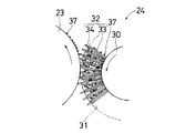
図1は、本発明の実施の一形態の概略的な構成を示す。現像装置21は現像ローラ23、供給ローラ24および現像剤規制部材であるブレード25を装着する現像剤容器27として、一体的に構成される。現像ローラ23および供給ローラ24は導電性であり、バイアス電源28,29から、それぞれ−350Vおよび−650Vの電圧がバイアス電圧として共通電位である接地電位との間で印加される。現像ローラ23の構成は、図10に示す従来からの現像ローラ3と基本的に同等である。供給ローラ24は、芯材30の周囲に植毛部31が形成されている。
【0032】
芯材30は、直円筒状であり、(a)金属製、(b)電気絶縁性の合成樹脂製筒体であって、その表面に導電層または半導電層を形成した構成、(c)電気絶縁性の紙製筒体であって、その表面に導電層または半導電層を形成した構成であってもよい。この導電層または半導電層は、めっきなどによって形成されてもよいが、後述の静電植毛法などにおける導電性または半導電性接着剤から成ってもよい。
【0033】
ブレード25は、そのエッジが現像ローラ23の表面から近接して離間し、現像ローラ23上の現像剤の付着量を規制しているけれども、図10のブレード5のように、先端部を当接させる形式であってもよい。
【0034】
図2は、図1の現像ローラ23に対して供給ローラ24が接触しているニップ部の状態を示す。植毛部31には、現像ローラ23の径方向に延びるファイバ32が一定の密度で植毛されている。現像剤37は、ファイバ32の間のすきまに保持される。ファイバ32の表面には導電性ポリマ層33が形成され、中心の電気絶縁性基材34の繊維を覆っている。ファイバ32の先端部では前記導電性ポリマ層33は除去されている。この先端部で導電性ポリマ層33が除去されているので、ファイバ32が直接に現像ローラ23の表面に接触しても通電状態とはならず、現像ローラ23および供給ローラ24のバイアス電圧は安定に維持される。ファイバ32はある程度の腰があるので、現像ローラ23上に残存している現像剤があれば、ストレスを与えることなく、はじき飛ばすようにして除去することができる。
【0035】
図3は、ファイバ32の形状を、(a)で示す本実施形態の場合と、(b)で示す全体的に導電性を有する比較例の場合とで比較して示す。図3(b)のように全体的に導電性を有するファイバ32では、カーボン層35などの導電性の層が電気絶縁性材料の層間に存在して基材自体に形成されている。このようなカーボン層35などの導電性部分を基材自体に形成することは、製造が困難であり、製造コストが上昇する原因となる。図3(a)に示す本実施形態の導電性ポリマ層33は、たとえばアキレス株式会社製の商品名「STポリ」などのポリピロール系導電性ポリマを好適に使用することができる。ポリピロール系導電性ポリマでは、ポリマ主鎖状に生成されるジカチオンなどが主鎖間を移動することによって電荷を運び、導電性を示すと考えられている。このようなポリピロールの層は、表面の厚み0.1〜0.5μmであり、このため素材の特性を殺すことなく導電性を付与することができる。導電性能は前述した電気抵抗102〜107Ωまで自由に設定することができる。導電性を付与する機構がジカチオンによる電子伝導性であるため、イオン伝導性の場合のように湿度によって導電性能が変化することがなく、安定に導電性を維持することができる。
【0036】
基材34としては、アクリル樹脂、ポリエステル、ナイロンなどの電気絶縁性合成樹脂製繊維を使用することができる。導電性ポリマ層33と基材34との接着性を向上させるために、必要に応じてプライマ処理することも可能である。基材34は、約3デニールであり、長さ1.0〜3.0mm、好ましくは1.2〜1.5mmであり、これによって芯材30の表面に密に静電植毛することができ、長すぎると、植毛密度が低下する。またファイバ32の先端部では、導電性ポリマ層33を除去して電気絶縁部36を形成する。
【0037】
図4は、図1の供給ローラ24の表面に植毛部31を、静電植毛法によって形成する工程を概略的に示す。芯材30の周囲に導電性もしくは半導電性の接着剤層39を塗布しておき、直流電源38によって図4の上下に間隔をあけた一対の平行平板電極41,42との間に高電圧を印加する。芯材30の水平軸線43は、水平な電極41,42に平行である。この電界内にある芯材30の軸線43を含む仮想上の鉛直一平面45に平行に電気力線が発生される。電源38の高電位側の電極41上には、予め定める同一長さの多数のファイバ32が乗載されている。芯材30と電極41との間には、合成樹脂などの電気絶縁性材料から成る平板状の制限部材43が介在される。この制限部材43にはスリット44が形成されるスリット44は芯材30の軸線43に平行に延びる。軸線43を含む仮想上の一平面45が、スリット44の軸線46を含む図4の状態では、電気力線に沿って細長く飛翔するファイバ32が、芯材30の径方向に、接着剤層39によって付着される。
【0038】
本発明の実施の他の形態では、制限部材43のスリット43を仮想上の一平面45から図4の左方または右方に変位して設置する。これによって芯材30の表面には、その芯材30の径方向に対して傾斜した姿勢で、ファイバ32を付着させることができる。
【0039】
この静電植毛時においては、芯材30は、矢符47の方向に回転され、したがってスリット44を通過してきたファイバ32が、芯材30の径方向に、またはその径方向に対して希望する角度で傾斜した状態でファイバ32を付着し、こうして芯材30の全周面にわたり植毛することができる。図4は、スリット44の軸線46は、前記仮想上の一平面45内にあり、しかも芯材30の軸線43に平行である状態が、図4に示されている。直流電源38の極性を、図4とは逆とし、ファイバ32を低電位側の電極に設けてもよい。
【0040】
ファイバ32の他端部である先端部に、図3(a)で示すような電気絶縁部36を形成するためには、前記接着後に、いったん形成される導電性ポリマ層33を機械的に除去したり、有機溶剤などによって除去することによって形成可能である。
【0041】
図5は、本実施形態による植毛を用いる供給ローラ24と、従来からの導電性スポンジを用いる供給ローラ4とで、感光体ドラムでの現像剤のかぶり量の推移についての実験結果の一例を示す。本発明の植毛供給ローラ24は、従来のスポンジを用いる供給ローラ4に比べて、感光体上かぶり濃度が小さく改善されていることがわかる。
【0042】
図6は、現像ローラ23に対する植毛供給ローラ24の食込み量における感光体上かぶり濃度への影響についての実験結果の一例を示す。図6に示すように、非接触および接触においても、感光体上かぶりが一定していることにより、現像剤へのストレスが小さいことが判断される。
【0043】
図7は、現像剤を介して供給ローラ24から現像ローラ23へ流れ込む電流値を示す。図7のように、本発明に従う植毛供給ローラ24を用いることによって、常に安定した電界を形成することが可能であることが理解される。これに対して従来のスポンジを用いる供給ローラ4では、リーク電流が流れ、現像剤に不要な電荷が与えられていると考えられる。
【0044】
図8は、現像ローラ23に対する植毛供給ローラ24の食込み量における現像剤の追従性についての実験結果の一例を示す。図8に示すように、非接触においても、現像剤の供給が行われ、接触によってより安定した現像剤の供給が行われている。スポンジ製供給ローラ4を用いた場合には、その食い込み量の変化によりかぶり濃度が大きく変化する。
【0045】
図9は、スポンジを用いる供給ローラ4と植毛供給ローラ24とを用いた場合の各々の現像ローラ23上の現像剤規制部材25を通過した後の現像剤層の電位を示している。この図9より、植毛供給ローラ24を用いた場合、その供給ローラ24に印加される電圧に拘わらず、現像剤層の電位が安定している。
【0046】
これに対してスポンジの供給ローラ4を用いた場合には、印加電圧により、現像剤層の電位が大きく変化しており、スポンジの供給ローラ4から現像剤に対し不要な電荷の注入があったり、あるいは電荷のリークがあることを示している。このことより、スポンジローラ自身の抵抗、スポンジのローラ4と現像ローラ23のニップ幅などにより、現像剤の電荷が大きく変化することを示唆している。本発明はこの問題を解決する。
【0047】
本発明は、現像ローラ23は、芯金の外周を導電性弾性ゴムなどの材料で構成し、感光体をドラム状の固いものとしての弾性接触についてであるが、ベルト状のフレキシブルな弾性感光体を用いる場合に、金属製の円筒状の現像ローラを感光体に接触して用い、この場合にも本発明は有効である。また、感光体と現像ローラとの間に所定の空隙を設け、その空隙を感光体の表面電位の差により現像剤を飛翔させる、いわゆるジャンピング現像方式にも使用できる。以上のように、本発明は現像ローラ上に非磁性一成分系トナーを供給するいかなる現像方式にも好適に使用することができ、また現像剤は、キャリアとトナーとから成る2成分系であってもよい。
【0048】
【発明の効果】
以上のように本発明によれば、供給ローラの表面にファイバを植毛して現像剤の搬送を行うので、現像剤に余分な機械的ストレスを与えず、現像剤の帯電量を安定に保ちながら、供給ローラから現像ローラまでの現像剤の移行を円滑かつ安定に行うことができる。供給ローラに導電性スポンジを用い、その凹部で現像剤を搬送する場合のように、現像剤が凹部に詰まって寿命を短縮させたり、現像剤に余分な機械的ストレスを与えたり現像剤の帯電量を変化させたりする恐れはなく、また供給ローラとしての製造も導電性スポンジを加工する場合に比較して安価に行うことができる。
また、ファイバの先端部は電気絶縁性を有するので、ファイバが導電性を有しても、現像ローラと供給ローラとの間の電界を安定に維持することができる。
【0049】
また本発明によれば、ファイバを静電植毛法によって供給ローラの表面に植毛するので、均一な植毛を安価に行うことができる。
【0050】
また本発明によれば、芯材またはファイバの少なくとも表面は、導電性または半導電性を有するので、供給ローラのチャージアップを防止して安定な現像剤の供給を行うことができる。
【0052】
また本発明によれば、導電性を有するファイバは、電気絶縁性または半導電性の基材の表面を導電性ポリマ層によって覆って形成するので、基材として導電性のファイバを使用する場合よりも安価に供給ローラを製造することができる。
【0053】
また本発明によれば、導電性ポリマが電子伝導性材料であるので、イオン伝導性のような湿度依存性がなく安定な現像剤の供給を行うことができる。
【0054】
また本発明によれば電子伝導性材料がポリピロール系導電性ポリマであるので、各種基材に導電性を付与し、イオン伝導性のような湿度依存性なく、安定に現像剤の供給を行うことができる。
【0055】
また本発明によれば、ファイバの先端部では導電性ポリマ層が除去されているので、現像ローラと供給ローラとの間の電界を安定に維持し、現像剤の供給を安定に継続することができる。
【0056】
さらに本発明によれば、現像装置には表面にファイバが植毛されている供給ローラと現像ローラとが含まれ、供給ローラの表面のファイバによって現像剤が現像ローラに安定に供給されるので、良好な品質の画像を形成する現像装置を得ることができる。
【0057】
本発明によれば、現像ローラと供給ローラとに所定の電圧を印加し、この電圧は、供給ローラと現像ローラとの印加電圧が同一であってもよく、あるいはまた相互に異ならせ、現像剤を供給ローラから現像ローラに移動する電界を形成する電圧に定める。
【0058】
現像剤として、非磁性一成分系トナーを用いることによって、構成が簡略化され、取扱いが容易となり、そのトナーは静電力によって円滑に移動して供給ローラから現像ローラに供給することができる。
【0059】
現像ローラは、感光体に接触していてもよく、または非接触であってもよく、現像ローラから感光体に静電力によって現像剤が移動して感光体上の静電潜像が顕像化される。
【0060】
また本発明によれば、現像ローラの表面に供給される現像剤は、現像剤規制部材によって付着量が規制されるので、余分な現像剤が現像に使用されず、良好な品質の画像を得ることができる。
【0061】
本発明によれば、静電植毛法によって、少なくとも表面が導電性となっている芯材の表面に、ファイバの一端部を付着することが容易に可能である。
【0062】
さらに本発明によれば、スリットを有する制限部材を用い、ファイバを傾斜する姿勢で芯材の表面に付着させることができ、これによってファイバの他端部を希望する状態で現像ローラに接触させて、現像剤の円滑な供給を可能にすることができる。
【図面の簡単な説明】
【図1】本発明の実施の一形態の概略的な構成を示す断面図である。
【図2】図1の現像ローラ23と供給ローラ24との接触部の拡大図である。
【図3】図1の実施形態の植毛部31のファイバ32の構造を示す断面図である。
【図4】図1の植毛部31を静電植毛法によって形成する状態を示す説明図である。
【図5】本実施形態による植毛供給ローラ24と従来からのスポンジを用いる供給ローラ4との間で、感光体ドラム上のかぶりの推移を比較した実験結果の一例を示すグラフである。
【図6】本実施形態の植毛供給ローラ24の現像ローラ23に対する食込み量の感光体上かぶりへの影響についての実験結果の一例を示すグラフである。
【図7】本実施形態の植毛供給ローラ24と従来からのスポンジを用いる供給ローラ4とにおける供給ローラ24,4への印加電圧と現像ローラへの漏れ電流との関係を示す実験結果の一例を示すグラフである。
【図8】本実施形態による植毛供給ローラ24の現像ローラ23に対する食込み量と現像剤の追従性との関係についての実験結果の一例を示すグラフである。
【図9】本実施形態による植毛供給ローラ24と従来からのスポンジを用いる供給ローラ4とにおける供給ローラ24,4への印加電圧と、現像剤規制部材25を通過した後の現像ローラ23上の現像剤層の電位との関係についての実験結果の一例を示すグラフである。
【図10】従来からの供給ローラ4および現像装置を示す簡略化した断面図である。
【図11】図10の供給ローラ4の製法を示す簡略化した斜視図である。
【図12】図10の現像ローラ3と供給ローラ4との間の接触部の概略的な断面図である。
【図13】図10の現像ローラ3と供給ローラ4との間の電気的接続状態を示す模式図である。
【符号の説明】
21 現像装置
23 現像ローラ
24 供給ローラ
25 現像剤規制部材
27 現像剤容器
28,29 バイアス電源
30 芯金
31 植毛部
32 ファイバ
33 導電性ポリマ層
34 電気絶縁性基材
36 電気絶縁部[0001]
BACKGROUND OF THE INVENTION
The present invention relates to a supply roller and a developing device used in an apparatus for image formation by an electrophotographic system such as a copying machine or a printer.
[0002]
[Prior art]
For example, an image forming apparatus such as an electrophotographic copying machine or a laser beam printer uses a developing
[0003]
Since the toner is physically conveyed to the surface of the developing
[0004]
FIG. 11 shows an outline of a method for manufacturing the supply roller 4. A
[0005]
FIG. 12 shows a state of the
[0006]
FIG. 13 shows a method for forming an electric field. A voltage that generates a potential difference necessary for developing the electrostatic latent image on the photosensitive member is applied to the developing
[0007]
The supply roller 4 used as described above is required to have the following characteristics.
(1) The toner charge is not leaked. For this reason, having an extremely conductive property is a harmful effect.
(2) It is necessary to select a material while paying attention to the triboelectric charging series so as not to give the toner of reverse polarity.
{Circle around (3)} The conductive roller needs to be appropriately conductive so that the supply roller 4 does not charge up.
(4) When the supply roller 4 is in contact with the developing roller, the supply roller strongly presses the toner against the developing
(5) In the system in which the supply roller 4 rubs the surface of the developing roller, scrapes off the toner on the contact surface, and refreshes, the state of the surface of the supply roller does not always change stably both electrically and mechanically. is required.
(6) It has electrical characteristics that do not affect the bias voltage applied to the developing
(7) Do not give the necessary mechanical stress to the toner.
(8) The material does not damage the developing
[0008]
[Problems to be solved by the invention]
The supply roller 4 having a surface coated with a conventional
[0009]
(1) It is not easy to control the foaming rate of the conductive sponge, and when the foaming rate changes, the hardness, the resistance value, and the number of cells on the surface easily change. It is difficult to produce a sponge with little variation by securing this predetermined characteristic.
{Circle around (2)} Since the conductive sponge itself is easily deformed, it is not easy to form the outer shape in a perfect circle at the time of manufacture. For example, the external accuracy of the sponge is about ± 0.2 mm. For example, assuming that the developing roller diameter is 20 mm and the supply roller diameter is 16 mm, with this accuracy, the nip width is about 3 mm to 5 mm when the amount of sponge encroachment is 0.5 ± 0.2 mm. This greatly affects the contact resistance and the frictional charging of the toner. Moreover, since such a process is required, manufacturing cost will increase.
(3) A sponge roller as the supply roller 4 is formed by mounting a
(4) If the
(5) In addition, if the pressing force on the surface of the supply roller against the developing
(6) If the pressing force on the surface of the supply roller 4 is large, unnecessary frictional charging and filming on the developing
[0010]
These phenomena appear as the following phenomena on an image formed by development.
(1) Density unevenness due to unstable toner supply.
(2) Change in density and increase in fog density due to change in toner characteristics.
[0011]
Further, when the
[0012]
In addition, in the contact charging system such as a charging roller or a charging brush, these toners are likely to adhere electrostatically, and the charging means is contaminated with these toners, and charging unevenness is caused without normal charging. It becomes easy to go. In particular, in the cleanerless system, the toner is not easily collected electrostatically by the developing
[0013]
Further, when a metal roller is used as the supply roller 4, the resistance value of the supply roller 4 is extremely low, so that the supply roller 4 is used without contact. As a result, the above-described problems caused by contact do not occur. However, in the case of a metal roller, the surface is substantially smooth, so the toner transportability is poor, and density unevenness tends to occur. In addition, since it is non-contact, in order to keep the electric field strength formed between the developing
[0014]
An object of the present invention is to solve the above-described problems, to provide a supply roller, a developing device, and a supply that are inexpensive, have a long life, stabilize the charge amount of the developer, and can suppress the generation of the reversely charged developer as much as possible. It is to provide a method for manufacturing a roller.
[0015]
[Means for Solving the Problems]
The present invention provides a supply roller for supplying a developer to an electrostatic latent image on a photosensitive member of an image forming apparatus using an electrophotographic system, and supplying the developer to a developing roller for visualizing,
Many fibers are implanted on the surface of the core material,
At least the surface of the fiber has conductivity or semiconductivity except for the tip,
The supply roller is characterized in that at least the surface of the tip of the fiber is electrically insulating.
According to the present invention, the surface of the supply roller is formed in a desired posture, that is, at an angle of greater than zero and less than 90 degrees with respect to the radial direction in the radial direction, that is, radially or on the surface of the core. Since the fibers are planted by the extending fiber, the developer can be held in the gap between the fibers, and a proper amount of the developer can be fed into the gap formed between the fiber of the developing roller and the supply roller. . Since the developer is pressed directly against the surface of the developing roller and is not rubbed at the contact or proximity region between the developing roller and the fiber of the supply roller, unnecessary frictional charging is applied to the developer or the developer Do not change the charge amount. Further, no mechanical stress is given to the developer.
Furthermore, since the fiber vibrates with the rotation of the supply roller, the developer adheres to the surface of the supply roller and there is no fear of shortening the service life, and the service life can be extended. Even in the case of refreshing where the developer on the developing roller is removed by the supply roller, it is possible to remove by removing the developer at the waist of the fiber as compared with the case where the conductive sponge layer is used to scrape in the surface contact state as in the past. Therefore, unnecessary stress is not given to the developer. Further, since there is almost no frictional resistance generated between the developing roller and the supply roller, the driving torque can be reduced.
In addition, since at least the surface of the tip of the conductive fiber has an electrical insulating part, even if the tip of the conductive fiber of the supply roller contacts the development roller, the developing roller and the supply roller are energized. However, each surface potential can be stably maintained.
[0016]
Further, the invention is characterized in that at least the surface of the core material is conductive or semiconductive.
Further, at least the surface of the fiber has conductivity or semiconductivity.
According to the present invention, since at least the surface of the core material and at least the surface of the fiber have conductivity or semiconductivity, a stable electric field can be formed with the developing roller, and supply is performed while preventing charge-up. The electrical characteristics of the roller can be maintained stably, and the amount of developer transferred from the supply roller to the developing roller can be stabilized. (A) At least the surface of the core material and the fiber may be conductive, or (b) at least the surface of the core material is conductive and at least the surface of the fiber is semiconductive. Or (c) vice versa, and (d) at least both the core and the fiber may be semiconductive. Conductivity means that the electrical resistance between one end of all fibers implanted in one supply roller and the other end of all fibers is 10. 6 -10 9 Less than Ω, semiconductive means 10 9 -10 12 Say Ω.
[0018]
In the present invention, the fiber has an electrically insulating or semiconductive base material and a conductive polymer layer covering the surface of the base material.
According to the present invention, the conductive fiber is formed so that the surface of the electrically insulating or semiconductive substrate is covered with the conductive polymer layer, so that it is easier than providing conductivity to the whole. And it can be manufactured at low cost.
[0019]
In the present invention, the conductive polymer is an electron conductive material. According to the present invention, since the conductive polymer is an electron conductive material, the humidity dependence of the electrical resistance value as in the case of ion conductivity is small, and stable use can be continued.
[0020]
In the present invention, the electron conductive material is a polypyrrole conductive polymer.
According to the present invention, since a polypyrrole-based conductive polymer is used as the electron conductive material, conductivity can be easily imparted to many types of substrates, and conductivity is imparted by ion conductivity. It can be used stably without dependency on humidity.
[0021]
Further, the conductive polymer layer is removed at the tip of the fiber of the present invention.
According to the present invention, since the conductive polymer layer is removed at the tip of the fiber, the electric field in the gap between the developing roller and the supply roller does not change even if the tip of the fiber contacts the developing roller. , Stable transfer of the developer can be performed smoothly.
[0022]
Further, the present invention provides a developing device for an electrophotographic image forming apparatus that visualizes an electrostatic latent image by supplying a developer onto a photoreceptor on which an electrostatic latent image is formed.
A container for storing developer;
A developing roller for supplying a developer onto the photoreceptor;
A large number of fibers are implanted on the surface of the core material, and a supply roller that supplies the developer in the container to the development roller,
At least the surface of the fiber has conductivity or semiconductivity except for the tip,
The developing device is characterized in that at least the surface of the tip of the fiber is electrically insulating.
According to the present invention, the developer conveyed between the fibers on the surface of the supply roller is smoothly transferred to the developing roller, and stable development can be performed.
[0023]
The present invention is characterized in that a predetermined voltage is applied to the developing roller and the supply roller.
Further, the present invention is characterized in that the voltage applied to the supply roller is determined to be the same voltage as the voltage applied to the developing roller or to a voltage that forms an electric field for supplying the developer to the developing roller.
According to the present invention, a predetermined voltage is applied to the developing roller having at least the surface conductive or semiconductive and the fiber having at least the surface of the supply roller conductive or semiconductive, and this voltage is The developing roller and the supply roller may have the same voltage, or are set to a voltage that forms an electric field in which the developer moves from the supply roller to the developer by an electrostatic force acting on the developer. Thus, the developer stored in the container is smoothly conveyed from the supply roller to the developing roller.
[0024]
In the invention, it is preferable that the developer is a non-magnetic one-component toner.
According to the present invention, the non-magnetic one-component developer is electrically insulating and can be moved smoothly by its electrostatic force. In addition, the non-magnetic property eliminates the adverse effect caused by an undesired magnetic field on the developer movement.
[0025]
According to the present invention, the developing roller is in contact with the photosensitive member.
In the invention, the developing roller is not in contact with the photosensitive member.
According to the present invention, the non-magnetic one-component toner or other developer adhering to the developing roller by the electrostatic force is smoothly transferred to the photosensitive member in contact with the developing roller, and is The electrostatic latent image can be visualized, or in the gap existing between the developing roller and the photoconductor, the developer flies from the developing roller to the photoconductor by an electrostatic force to be visualized.
[0026]
In addition, the present invention includes a developer regulating member that abuts or is close to the peripheral surface of the developing roller and regulates the amount of the developer supplied by the supply roller.
According to the present invention, the developer regulating member that regulates the amount of developer adhered contacts or closes with a gap, so the thickness of the developer layer adhering to the peripheral surface of the developing roller is regulated, The quality of the formed image can be improved by preventing the excess developer from transferring to the developing photoreceptor.
[0027]
Furthermore, the present invention forms an electric field by connecting a DC power source between a pair of electrodes,
In this electric field, at least the surface is coated with an adhesive on the surface of the long core material that is conductive or semiconductive, and is disposed.
While rotating the core around the axis of the core,
Among a pair of electrodes, from the high potential side electrode, at least the surface is made to fly a large number of fibers that are conductive or semiconductive by electrostatic force, and one end of the fiber is attached to the core,
A limiting member made of an electrically insulating material having a slit extending along the axis of the core material is disposed between the core material and the electrode on the high potential side,
A method of manufacturing a supply roller used in a developing device for an electrophotographic image forming apparatus, wherein a fiber that has passed through the slit is attached to the surface of a core material in an inclined posture.
The adhesive may be electrically conductive but may be electrically insulating. In the case where at least the outer peripheral surface of the fiber is conductive or semiconductive, even if the adhesive is electrically insulating, the one end of the fiber penetrates the electrically insulating adhesive and the conductivity of the core material Alternatively, electrical connection is made by contacting the semiconductive surface.
According to the present invention, since the fiber is implanted on the surface of the supply roller by the electrostatic flocking method, uniform flocking can be performed with high productivity, and the supply roller can be manufactured at low cost.
[0028]
Furthermore, the present invention forms an electric field by connecting a DC power source between a pair of electrodes,
In this electric field, an adhesive is applied to the surface of the long core material and arranged,
While rotating the core around the axis of the core,
Among a pair of electrodes, from the high potential side electrode, at least the surface is made to fly a large number of fibers that are conductive or semiconductive by electrostatic force, and one end of the fiber is attached to the core,
A limiting member made of an electrically insulating material having a slit extending along the axis of the core material is disposed between the core material and the electrode on the high potential side,
A method of manufacturing a supply roller used in a developing device for an electrophotographic image forming apparatus, wherein a fiber that has passed through the slit is attached to the surface of a core material in an inclined posture.
If the core material is made of a material such as synthetic resin or paper, and is electrically insulating, a conductive adhesive is used. At least the surface of the core material may be conductive.
In each of the above claims, the fiber may be conductive or semiconductive at least on its surface, or the entire fiber may be electrically insulating, or may be conductive or semiconductive.
[0029]
Furthermore, a limiting member made of an electrically insulating material having a slit extending along the axis of the core material is disposed between the core material and the electrode on the high potential side,
The fiber that has passed through the slit is attached to the surface of the core material in an inclined posture.
The limiting member has, for example, a flat plate shape, and has a long and narrow slit parallel to the axis of the long core material. The fiber passing through the slit is attached to the core material with an adhesive. In the configuration in which the axis of the core material and the axis of the elongated slit exist in one virtual plane, when there is an electric field line in the electric field in the virtual plane, the line is elongated along the electric field line. The fiber flying in an extended state is attached to one end of the fiber in a posture extending in the radial direction of the core material in a natural state. When the virtual plane and the electric force line passing through the axis of the slit intersect, the fiber flying in a state extending along the electric force line passes through the slit, and the fiber extends in a natural state. Is attached to one end of the fiber in an oblique posture intersecting at an angle of more than zero and 90 degrees or less of the tangent to the radial direction of the core material. The fibers that have reached the core member and adhered obliquely in this way are preferably used in accordance with the rotational directions of the supply roller and the developing roller, and can smoothly transport the developer.
[0030]
In the present invention, the fiber is formed by forming a conductive layer on the surface of an electrically insulating or semiconductive substrate.
After attaching one end of the fiber to the surface of the core material, the conductive layer near the other end of the fiber is removed.
The other end of the fiber is prevented from disturbing the electric field for transporting the developer due to contact of the conductive portion of at least the surface of the fiber with the developing roller, or the other end of the fiber. It is possible to prevent the electric field from being disturbed even when the electrically insulating portion of the portion stably contacts the developing roller. As a result, the visualization with the developer is stably performed, and the image quality is improved.
[0031]
DETAILED DESCRIPTION OF THE INVENTION
FIG. 1 shows a schematic configuration of an embodiment of the present invention. The developing
[0032]
The
[0033]
Although the
[0034]
FIG. 2 shows a state of the nip portion where the
[0035]
FIG. 3 shows the shape of the
[0036]
As the
[0037]
FIG. 4 schematically shows a process of forming the flocked
[0038]
In another embodiment of the present invention, the
[0039]
At the time of electrostatic flocking, the
[0040]
In order to form the electrical insulating
[0041]
FIG. 5 shows an example of an experimental result regarding the transition of the developer fogging amount on the photosensitive drum by the
[0042]
FIG. 6 shows an example of an experimental result on the influence of the amount of biting of the
[0043]
FIG. 7 shows a current value flowing from the
[0044]
FIG. 8 shows an example of an experimental result on the followability of the developer in the amount of biting of the
[0045]
FIG. 9 shows the potential of the developer layer after passing through the
[0046]
On the other hand, when the sponge supply roller 4 is used, the potential of the developer layer varies greatly depending on the applied voltage, and unnecessary charge is injected from the sponge supply roller 4 to the developer. Or there is a charge leak. This suggests that the charge of the developer varies greatly depending on the resistance of the sponge roller itself, the nip width between the sponge roller 4 and the developing
[0047]
The present invention relates to the elastic contact of the developing
[0048]
【The invention's effect】
As described above, according to the present invention, the developer is transported by flocking the fiber on the surface of the supply roller, so that an excessive mechanical stress is not given to the developer and the charge amount of the developer is kept stable. The transfer of the developer from the supply roller to the developing roller can be performed smoothly and stably. As in the case where a conductive sponge is used for the supply roller and the developer is conveyed in the recess, the developer is clogged in the recess to shorten the service life, and the developer is charged with extra mechanical stress or charged with the developer. There is no fear of changing the amount, and the supply roller can be manufactured at a lower cost as compared with the case of processing the conductive sponge.
Further, since the tip of the fiber has electrical insulation, the electric field between the developing roller and the supply roller can be stably maintained even if the fiber has conductivity.
[0049]
Further, according to the present invention, since the fiber is implanted on the surface of the supply roller by the electrostatic flocking method, uniform flocking can be performed at a low cost.
[0050]
Further, according to the present invention, since at least the surface of the core material or fiber has conductivity or semiconductivity, the supply roller can be prevented from being charged up and a stable developer can be supplied.
[0052]
Further, according to the present invention, the conductive fiber is formed by covering the surface of the electrically insulating or semiconductive base material with the conductive polymer layer, so that the conductive fiber is used as the base material. Also, the supply roller can be manufactured at a low cost.
[0053]
In addition, according to the present invention, since the conductive polymer is an electron conductive material, it is possible to supply a stable developer without humidity dependency like ion conductivity.
[0054]
In addition, according to the present invention, since the electron conductive material is a polypyrrole-based conductive polymer, it is possible to provide conductivity to various base materials and to supply a developer stably without dependency on humidity such as ion conductivity. Can do.
[0055]
Further, according to the present invention, since the conductive polymer layer is removed at the tip of the fiber, the electric field between the developing roller and the supply roller can be stably maintained, and the supply of the developer can be stably continued. it can.
[0056]
Further, according to the present invention, the developing device includes a supply roller having a fiber implanted on the surface and a developing roller, and the developer is stably supplied to the developing roller by the fiber on the surface of the supply roller. It is possible to obtain a developing device that forms an image of a high quality.
[0057]
According to the present invention, a predetermined voltage is applied to the developing roller and the supply roller, and the voltage applied to the supply roller and the developing roller may be the same or different from each other. Is set to a voltage that forms an electric field that moves from the supply roller to the developing roller.
[0058]
By using a non-magnetic one-component toner as the developer, the configuration is simplified and the handling becomes easy, and the toner can be smoothly moved by an electrostatic force and supplied from the supply roller to the development roller.
[0059]
The developing roller may be in contact with the photosensitive member or may be non-contacting. The developer moves from the developing roller to the photosensitive member by electrostatic force, and the electrostatic latent image on the photosensitive member is visualized. Is done.
[0060]
Further, according to the present invention, since the amount of the developer supplied to the surface of the developing roller is regulated by the developer regulating member, excess developer is not used for development, and a good quality image is obtained. be able to.
[0061]
According to the present invention, it is possible to easily attach one end of the fiber to at least the surface of the core material having a conductive surface by electrostatic flocking.
[0062]
Furthermore, according to the present invention, the limiting member having the slit can be used to attach the fiber to the surface of the core material in an inclined posture, and thereby the other end of the fiber is brought into contact with the developing roller in a desired state. , Smooth supply of the developer can be made possible.
[Brief description of the drawings]
FIG. 1 is a cross-sectional view showing a schematic configuration of an embodiment of the present invention.
2 is an enlarged view of a contact portion between a developing
3 is a cross-sectional view showing the structure of the
4 is an explanatory view showing a state in which the hair-implanted
FIG. 5 is a graph showing an example of experimental results comparing the transition of fog on the photosensitive drum between the flocking
FIG. 6 is a graph showing an example of an experimental result on the influence of the amount of biting on the developing
FIG. 7 shows an example of experimental results showing the relationship between the voltage applied to the
FIG. 8 is a graph showing an example of experimental results on the relationship between the amount of biting into the developing
FIG. 9 shows a voltage applied to the
FIG. 10 is a simplified cross-sectional view showing a conventional supply roller 4 and a developing device.
11 is a simplified perspective view showing a manufacturing method of the supply roller 4 of FIG.
12 is a schematic cross-sectional view of a contact portion between the developing
13 is a schematic diagram showing an electrical connection state between the developing
[Explanation of symbols]
21 Developer
23 Development roller
24 Supply roller
25 Developer regulating member
27 Developer container
28, 29 Bias power supply
30 cored bar
31 Flocking
32 fiber
33 Conductive polymer layer
34 Electrically insulating substrate
36 Electrical insulation
Claims (21)
芯材の表面に、多数のファイバが植毛されているとともに、
ファイバの少なくとも表面は、先端部を除いて導電性または半導電性を有し、
ファイバの先端部の少なくとも表面は電気絶縁性であることを特徴とする供給ローラ。In a supply roller for supplying a developer to an electrostatic latent image on a photoreceptor of an image forming apparatus using an electrophotographic method, and supplying the developer to a developing roller for visualizing,
Many fibers are implanted on the surface of the core material,
At least the surface of the fiber has conductivity or semiconductivity except for the tip,
A supply roller characterized in that at least the surface of the tip of the fiber is electrically insulating.
現像剤を貯留する容器と、
感光体上に現像剤を供給する現像ローラと、
芯材の表面に、多数のファイバが植毛され、容器内の現像剤を現像ローラに供給する供給ローラとを含み、
ファイバの少なくとも表面は、先端部を除いて導電性または半導電性を有し、
ファイバの先端部の少なくとも表面は電気絶縁性であることを特徴とする現像装置。In a developing device for an electrophotographic image forming apparatus in which a developer is supplied onto a photoreceptor on which an electrostatic latent image is formed to visualize the electrostatic latent image.
A container for storing developer;
A developing roller for supplying a developer onto the photoreceptor;
A large number of fibers are implanted on the surface of the core material, and a supply roller that supplies the developer in the container to the development roller,
At least the surface of the fiber has conductivity or semiconductivity except for the tip,
A developing device characterized in that at least the surface of the tip of the fiber is electrically insulating.
この電界内に、少なくとも表面が導電性または半導電性である長尺の芯材の前記表面に接着剤を塗布して、配置し、
芯材を、その芯材の軸線まわりに回転しつつ、
一対の電極のうち、高電位側の電極上から、少なくとも表面が導電性または半導電性である多数のファイバを、静電力によって飛翔させて、そのファイバの一端部を、芯材に付着させ、
芯材と、前記高電位側の電極との間に、芯材の軸線に沿って延びるスリットを有する電気絶縁性材料から成る制限部材を配置し、
前記スリットを通過したファイバを、芯材の表面に、傾斜する姿勢で付着させることを特徴とする電子写真方式画像形成装置のための現像装置に用いられる供給ローラの製造方法。Connect a DC power supply between a pair of electrodes to form an electric field,
In this electric field, at least the surface is coated with an adhesive on the surface of the long core material that is conductive or semiconductive, and is disposed.
While rotating the core around the axis of the core,
Among a pair of electrodes, from the high potential side electrode, at least the surface is made to fly a large number of fibers that are conductive or semiconductive by electrostatic force, and one end of the fiber is attached to the core,
A limiting member made of an electrically insulating material having a slit extending along the axis of the core material is disposed between the core material and the electrode on the high potential side,
A method of manufacturing a supply roller used in a developing device for an electrophotographic image forming apparatus, wherein the fiber that has passed through the slit is attached to the surface of a core material in an inclined posture.
この電界内に、長尺の芯材の前記表面に接着剤を塗布して、配置し、
芯材を、その芯材の軸線まわりに回転しつつ、
一対の電極のうち、高電位側の電極上から、少なくとも表面が導電性または半導電性である多数のファイバを、静電力によって飛翔させて、そのファイバの一端部を、芯材に付着させ、
芯材と、前記高電位側の電極との間に、芯材の軸線に沿って延びるスリットを有する電気絶縁性材料から成る制限部材を配置し、
前記スリットを通過したファイバを、芯材の表面に、傾斜する姿勢で付着させることを特徴とする電子写真方式画像形成装置のための現像装置に用いられる供給ローラの製造方法。Connect a DC power supply between a pair of electrodes to form an electric field,
In this electric field, an adhesive is applied to the surface of the long core material and arranged,
While rotating the core around the axis of the core,
Among a pair of electrodes, from the high potential side electrode, at least the surface is made to fly a large number of fibers that are conductive or semiconductive by electrostatic force, and one end of the fiber is attached to the core,
A limiting member made of an electrically insulating material having a slit extending along the axis of the core material is disposed between the core material and the electrode on the high potential side,
A method of manufacturing a supply roller used in a developing device for an electrophotographic image forming apparatus, wherein the fiber that has passed through the slit is attached to the surface of a core material in an inclined posture.
芯材の表面にファイバの一端部を付着させた後に、ファイバの他端部付近の導電層を除去することを特徴とする請求項19または20に記載の電子写真方式画像形成装置のための現像装置に用いられる供給ローラの製造方法。The fiber is configured by forming a conductive layer on the surface of an electrically insulating or semiconductive material,
21. The development for an electrophotographic image forming apparatus according to claim 19, wherein after the one end of the fiber is attached to the surface of the core member, the conductive layer near the other end of the fiber is removed. Manufacturing method of supply roller used in apparatus.
Priority Applications (1)
| Application Number | Priority Date | Filing Date | Title |
|---|---|---|---|
| JP27963596A JP3665433B2 (en) | 1996-10-22 | 1996-10-22 | Supply roller and developing device |
Applications Claiming Priority (1)
| Application Number | Priority Date | Filing Date | Title |
|---|---|---|---|
| JP27963596A JP3665433B2 (en) | 1996-10-22 | 1996-10-22 | Supply roller and developing device |
Publications (2)
| Publication Number | Publication Date |
|---|---|
| JPH10123821A JPH10123821A (en) | 1998-05-15 |
| JP3665433B2 true JP3665433B2 (en) | 2005-06-29 |
Family
ID=17613735
Family Applications (1)
| Application Number | Title | Priority Date | Filing Date |
|---|---|---|---|
| JP27963596A Expired - Lifetime JP3665433B2 (en) | 1996-10-22 | 1996-10-22 | Supply roller and developing device |
Country Status (1)
| Country | Link |
|---|---|
| JP (1) | JP3665433B2 (en) |
Families Citing this family (4)
| Publication number | Priority date | Publication date | Assignee | Title |
|---|---|---|---|---|
| JP2003345120A (en) * | 2002-05-29 | 2003-12-03 | T & M Kk | Developing device |
| JP2007147924A (en) * | 2005-11-25 | 2007-06-14 | Katsuragawa Electric Co Ltd | Developing device |
| CN102239293A (en) | 2008-12-02 | 2011-11-09 | 东丽株式会社 | Electrically conductive floc and electrically conductive brush |
| CN102323729B (en) * | 2011-09-29 | 2013-12-04 | 深圳市乐普泰科技股份有限公司 | Powder feed roll of double-layer structure and manufacturing method thereof |
-
1996
- 1996-10-22 JP JP27963596A patent/JP3665433B2/en not_active Expired - Lifetime
Also Published As
| Publication number | Publication date |
|---|---|
| JPH10123821A (en) | 1998-05-15 |
Similar Documents
| Publication | Publication Date | Title |
|---|---|---|
| JP4183216B2 (en) | Developing roller and developing device thereof | |
| US5196892A (en) | Image forming apparatus having a disordering and charging device for disordering a developing agent remaining on an image bearing member and for charging the image bearing member | |
| JPS63100482A (en) | Toner carrier | |
| JP2921962B2 (en) | Developing device | |
| JP2004117960A (en) | Image forming apparatus | |
| JP3996363B2 (en) | Development device | |
| JP3665433B2 (en) | Supply roller and developing device | |
| CN201373979Y (en) | Powder supply roller and developing device | |
| US7082277B2 (en) | Contact charger and image forming apparatus | |
| JP2000081782A (en) | Developing device | |
| JPH1063069A (en) | Image forming device | |
| JPH0240683A (en) | Cleaning device, transfer device, electrostatically charging device, destaticizing device and electrostatic latent image forming device | |
| JP4035266B2 (en) | Development device | |
| JPH06118855A (en) | Image forming device | |
| JPH09114183A (en) | Friction electrifying device | |
| JP2011081039A (en) | Image forming apparatus | |
| JP3637199B2 (en) | Image forming apparatus | |
| JP3278021B2 (en) | Image forming device | |
| JP2000081822A (en) | Image forming device | |
| JP2007178599A (en) | Image forming apparatus and image forming method | |
| JP2003021964A (en) | Developing device, and process cartridge and image forming device equipped with developing device | |
| JP2004004380A (en) | Development apparatus, process cartridge, and image forming apparatus | |
| JPH05323766A (en) | Electrostatic charging device | |
| JPH0915964A (en) | Developing unit | |
| JPH0915970A (en) | Developing device and method therefor |
Legal Events
| Date | Code | Title | Description |
|---|---|---|---|
| A131 | Notification of reasons for refusal |
Free format text: JAPANESE INTERMEDIATE CODE: A131 Effective date: 20040803 |
|
| A521 | Written amendment |
Free format text: JAPANESE INTERMEDIATE CODE: A523 Effective date: 20041004 |
|
| TRDD | Decision of grant or rejection written | ||
| A01 | Written decision to grant a patent or to grant a registration (utility model) |
Free format text: JAPANESE INTERMEDIATE CODE: A01 Effective date: 20050308 |
|
| A61 | First payment of annual fees (during grant procedure) |
Free format text: JAPANESE INTERMEDIATE CODE: A61 Effective date: 20050401 |
|
| R150 | Certificate of patent or registration of utility model |
Free format text: JAPANESE INTERMEDIATE CODE: R150 |
|
| S111 | Request for change of ownership or part of ownership |
Free format text: JAPANESE INTERMEDIATE CODE: R313113 |
|
| R350 | Written notification of registration of transfer |
Free format text: JAPANESE INTERMEDIATE CODE: R350 |
|
| FPAY | Renewal fee payment (event date is renewal date of database) |
Free format text: PAYMENT UNTIL: 20080408 Year of fee payment: 3 |
|
| FPAY | Renewal fee payment (event date is renewal date of database) |
Free format text: PAYMENT UNTIL: 20090408 Year of fee payment: 4 |
|
| FPAY | Renewal fee payment (event date is renewal date of database) |
Free format text: PAYMENT UNTIL: 20100408 Year of fee payment: 5 |
|
| FPAY | Renewal fee payment (event date is renewal date of database) |
Free format text: PAYMENT UNTIL: 20100408 Year of fee payment: 5 |
|
| FPAY | Renewal fee payment (event date is renewal date of database) |
Free format text: PAYMENT UNTIL: 20110408 Year of fee payment: 6 |
|
| FPAY | Renewal fee payment (event date is renewal date of database) |
Free format text: PAYMENT UNTIL: 20110408 Year of fee payment: 6 |
|
| FPAY | Renewal fee payment (event date is renewal date of database) |
Free format text: PAYMENT UNTIL: 20120408 Year of fee payment: 7 |
|
| FPAY | Renewal fee payment (event date is renewal date of database) |
Free format text: PAYMENT UNTIL: 20130408 Year of fee payment: 8 |
|
| FPAY | Renewal fee payment (event date is renewal date of database) |
Free format text: PAYMENT UNTIL: 20140408 Year of fee payment: 9 |
|
| R250 | Receipt of annual fees |
Free format text: JAPANESE INTERMEDIATE CODE: R250 |
|
| R250 | Receipt of annual fees |
Free format text: JAPANESE INTERMEDIATE CODE: R250 |
|
| R250 | Receipt of annual fees |
Free format text: JAPANESE INTERMEDIATE CODE: R250 |
|
| EXPY | Cancellation because of completion of term |