JP3654274B2 - Data transfer control device, electronic device, and power supply switching method - Google Patents
Data transfer control device, electronic device, and power supply switching method Download PDFInfo
- Publication number
- JP3654274B2 JP3654274B2 JP2002253382A JP2002253382A JP3654274B2 JP 3654274 B2 JP3654274 B2 JP 3654274B2 JP 2002253382 A JP2002253382 A JP 2002253382A JP 2002253382 A JP2002253382 A JP 2002253382A JP 3654274 B2 JP3654274 B2 JP 3654274B2
- Authority
- JP
- Japan
- Prior art keywords
- data transfer
- line
- power
- power supply
- vbus
- Prior art date
- Legal status (The legal status is an assumption and is not a legal conclusion. Google has not performed a legal analysis and makes no representation as to the accuracy of the status listed.)
- Expired - Fee Related
Links
- 238000012546 transfer Methods 0.000 title claims description 247
- 238000000034 method Methods 0.000 title claims description 36
- 238000012545 processing Methods 0.000 claims description 80
- 230000002093 peripheral effect Effects 0.000 claims description 49
- 230000007704 transition Effects 0.000 claims description 42
- 238000001514 detection method Methods 0.000 claims description 37
- 230000008569 process Effects 0.000 claims description 9
- 230000000977 initiatory effect Effects 0.000 claims 2
- 238000010586 diagram Methods 0.000 description 17
- 230000009977 dual effect Effects 0.000 description 11
- MHABMANUFPZXEB-UHFFFAOYSA-N O-demethyl-aloesaponarin I Natural products O=C1C2=CC=CC(O)=C2C(=O)C2=C1C=C(O)C(C(O)=O)=C2C MHABMANUFPZXEB-UHFFFAOYSA-N 0.000 description 7
- 239000011717 all-trans-retinol Substances 0.000 description 4
- FPIPGXGPPPQFEQ-OVSJKPMPSA-N all-trans-retinol Chemical compound OC\C=C(/C)\C=C\C=C(/C)\C=C\C1=C(C)CCCC1(C)C FPIPGXGPPPQFEQ-OVSJKPMPSA-N 0.000 description 4
- 230000004044 response Effects 0.000 description 3
- 230000008859 change Effects 0.000 description 2
- 230000003287 optical effect Effects 0.000 description 2
- 102100036848 C-C motif chemokine 20 Human genes 0.000 description 1
- 101000713099 Homo sapiens C-C motif chemokine 20 Proteins 0.000 description 1
- 101000911772 Homo sapiens Hsc70-interacting protein Proteins 0.000 description 1
- 230000002159 abnormal effect Effects 0.000 description 1
- 230000005540 biological transmission Effects 0.000 description 1
- 239000000470 constituent Substances 0.000 description 1
- 238000012937 correction Methods 0.000 description 1
- 238000013500 data storage Methods 0.000 description 1
- 230000007423 decrease Effects 0.000 description 1
- 238000003384 imaging method Methods 0.000 description 1
- 238000007726 management method Methods 0.000 description 1
- 238000012986 modification Methods 0.000 description 1
- 230000004048 modification Effects 0.000 description 1
- 239000002699 waste material Substances 0.000 description 1
Images


Classifications
-
- G—PHYSICS
- G06—COMPUTING; CALCULATING OR COUNTING
- G06F—ELECTRIC DIGITAL DATA PROCESSING
- G06F1/00—Details not covered by groups G06F3/00 - G06F13/00 and G06F21/00
- G06F1/26—Power supply means, e.g. regulation thereof
- G06F1/263—Arrangements for using multiple switchable power supplies, e.g. battery and AC
-
- G—PHYSICS
- G06—COMPUTING; CALCULATING OR COUNTING
- G06F—ELECTRIC DIGITAL DATA PROCESSING
- G06F1/00—Details not covered by groups G06F3/00 - G06F13/00 and G06F21/00
- G06F1/26—Power supply means, e.g. regulation thereof
- G06F1/266—Arrangements to supply power to external peripherals either directly from the computer or under computer control, e.g. supply of power through the communication port, computer controlled power-strips
Landscapes
- Engineering & Computer Science (AREA)
- Theoretical Computer Science (AREA)
- General Engineering & Computer Science (AREA)
- Physics & Mathematics (AREA)
- General Physics & Mathematics (AREA)
- Computer Hardware Design (AREA)
- Power Engineering (AREA)
- Power Sources (AREA)
- Information Transfer Systems (AREA)
Description
【0001】
【発明の属する技術分野】
本発明は、データ転送制御装置、電子機器及び電源切替方法に関する。
【0002】
【背景技術及び発明が解決しようとする課題】
近年、パーソナルコンピュータと周辺機器(広義には電子機器)とを接続するためのインタフェース規格として、USB(Universal Serial Bus)規格が注目を集めている。ところが、USB規格では必ずホストが必要であり、これまで周辺機器間でUSB規格のデータ転送を行うことができなかった。そこでUSB2.0規格の追加規格として、「USB On−The−Go(OTG)1.0」規格(以下では、OTG規格と略す。)が策定され、周辺機器間でもUSB規格のデータ転送を行うことができる。
【0003】
OTG規格では、USB規格におけるデバイスとして動作するペリフェラルに、ホストとして動作するために必要なホスト機能を持たせることができる。これによって、従来のUSB規格におけるデバイスだった周辺機器同士を相互に接続することができ、従来のUSB規格におけるホストを介することなく、データ転送を行うことができる。
【0004】
そのためOTG規格では、デュアルロールデバイス(Dual-role Device)とペリフェラルオンリーデバイス(Peripheral-only Device)とが規定される。デュアルロールデバイスとなる機器は、ホストとしてもペリフェラルとしても動作することができる。またペリフェラルオンリーデバイスとなる機器は、ペリフェラルとしてのみ動作することができる。
【0005】
ところでOTG規格では、消費電力を削減するため、例えばホストとして動作中のデバイスがバスを使用しないときは電源ラインの駆動を停止することができる。そこで、例えばペリフェラルとして動作中のデバイスが未使用中のバスを使用したいときは、ホストとして動作するデバイス側に対して使用を要求するSRP(Session Request Protocol)という手順により当該バスを使用することができる。SRPでは、データラインパルシング又はVBUS(電源バス)パルシングと呼ばれる手法で、ペリフェラルとして動作するデバイスが、ホストとして動作するデバイスに対しVBUSラインに電源を供給するように要求することになる。その結果として、OTG規格に準拠したデバイスでは、上述のSRPをイニシエート(initiate)するため、セルフパワー電源であることが必要とされる。
【0006】
ここで、OTG規格に準拠したデバイス(OTGデバイス)が、USB規格に準拠した標準ホスト(例えばパーソナルコンピュータ)に接続される場合を考える。規格上、標準ホストはVBUSラインに電源を供給する必要がある。ところがOTGデバイスはセルフパワー電源であるため、標準ホストからVBUSラインに対し常に電源が供給されているにも関わらず、OTGデバイスは自己の電源からの電力を消費して動作することになり、無駄な電力を消費していたという問題があった。特に、OTGデバイスが携帯型の情報機器である場合には、バッテリの寿命が短くなってしまう。
【0007】
本発明は、以上のような技術的課題に鑑みてなされたものであり、その目的とするところは、例えばOTG規格の周辺機器同士のデータ転送を行う場合に無駄な電力消費を削減するデータ転送制御装置、電子機器及び電源切替方法を提供することにある。
【0008】
【課題を解決するための手段】
上記課題を解決するために本発明は、デフォルト状態においてセルフパワー電源によりデータ転送制御を行う第1のデバイスのステート遷移又はデフォルト状態においてバスパワー電源によりデータ転送制御を行う第2のデバイスのステート遷移により、ホスト及びペリフェラルのステートの切り替え制御を行って、データライン及び電源ラインを介してデータの転送制御を行うデータ転送制御装置であって、電源回路と、前記第1のデバイスとしての動作時に前記電源ラインと前記電源回路とを接続する給電スイッチ回路と、前記データラインを介してデータ転送を行うデータ転送処理回路と、所与の切替信号に基づいて、前記電源ライン又は前記電源回路のいずれかから前記データ転送処理回路に対して電源を供給するための電源切替回路とを含むデータ転送制御装置に関係する。
【0009】
本発明においては、第1のデバイスとして動作するときは給電スイッチ回路により電源ラインに電源を供給するデータ転送制御装置において、電源切替回路により電源回路から電源ラインに切り替えてデータ転送処理回路に対して電源を供給することができる。したがって、例えば第2のデバイスとして動作するときに、電源ラインからの電源供給でデータ処理回路を動作させることができるので、電源回路の電力消費を削減することができる。
【0010】
また本発明に係るデータ転送制御装置は、前記所与の切替信号をオン又はオフにする切替スイッチ回路を含み、前記所与の切替信号は、前記切替スイッチ回路の出力に基づいて生成されてもよい。
【0011】
本発明によれば、切替スイッチ回路により適宜電源供給元を切り替えることができるのでデータ転送制御装置の消費電力の最適化を図ることができる。
【0012】
また本発明は、USB(Universal Serial Bus)のOTG(On-The-Go)規格に従ってデータ転送を制御するデータ転送制御装置であって、電源回路と、Aデバイスとしての動作時にVBUSラインと前記電源回路とを接続する給電スイッチ回路と、データラインを介してデータ転送を行うデータ転送処理回路と、所与の切替信号に基づいて、前記VBUSライン又は前記電源回路のいずれかから前記データ転送処理回路に対して電源を供給するための電源切替回路とを含み、前記電源切替回路は、Bデバイスとしての動作時のアイドル状態において前記VBUSラインの電圧が第1の閾値を超えたと判断された場合に、前記データ転送処理回路に対して前記VBUSラインから電源を供給するデータ転送制御装置に関係する。
【0013】
OTG規格に準拠したデータ転送制御装置では、セルフパワー電源であることが必要とされる。したがって例えば標準ホストによりVBUSラインに電源が供給されている場合でも、当該データ転送制御装置では自己の電源回路の電力を消費することになってしまう。
【0014】
本発明によれば、電源切替回路により、データ処理回路に対し、電源ラインから電源を供給してバスパワー電源で動作させることができるので、セルフパワー電源として搭載される電源回路の無駄な電力消費を削減することができる。またステート遷移結果により電源切替回路を動作させることができるので、特に大規模な付加回路を設けることなく電源切替の最適化を図ることができる。
【0015】
また本発明は、デフォルト状態においてセルフパワー電源によりデータ転送制御を行う第1のデバイスのステート遷移又はデフォルト状態においてバスパワー電源によりデータ転送制御を行う第2のデバイスのステート遷移により、ホスト及びペリフェラルのステートの切り替え制御を行って、データライン及び電源ラインを介してデータの転送制御を行うデータ転送制御装置であって、電源回路と、前記第1のデバイスとしての動作時に前記電源ラインと前記電源回路とを接続する給電スイッチ回路と、前記データラインを介してデータ転送を行うデータ転送処理回路と、前記電源ラインの電圧が第2の閾値を超えたか否かを検出する電源ライン電圧検出回路と、所与の切替信号に基づいて、前記電源ライン又は前記電源回路のいずれかから前記データ転送処理回路に対して電源を供給するための電源切替回路とを含み、前記電源切替回路は、前記第2のデバイスとして動作し、かつ前記電源ラインの電圧が前記第2の閾値より低い第1の閾値を超えていると判断された場合に、前記電源ラインから前記データ転送処理回路に対して電源を供給し、前記電源ラインの電圧が前記第2の閾値を超えていないと判断された場合に、前記データ転送処理回路に対して前記電源回路から電源を供給するデータ転送制御装置に関係する。
【0016】
また本発明は、USB(Universal Serial Bus)のOTG(On-The-Go)規格に従ってデータ転送を制御するデータ転送制御装置であって、Aデバイスとしての動作時にVBUSラインと前記電源回路とを接続する給電スイッチ回路と、データラインを介してデータ転送を行うデータ転送処理回路と、前記VBUSラインの電圧が第2の閾値を超えたか否かを検出する電源ライン電圧検出回路と、所与の切替信号に基づいて、前記VBUSライン又は前記電源回路のいずれかから前記データ転送処理回路に対して電源を供給するための電源切替回路とを含み、前記電源切替回路は、Bデバイスとして動作し、かつ前記VBUSラインの電圧が前記第2の閾値より低い第1の閾値を超えていると判断された場合に、前記データ転送処理回路に対して前記VBUSラインから電源を供給し、前記VBUSラインの電圧が前記第2の閾値を超えていないと判断された場合に、前記データ転送処理回路に対して前記電源回路から電源を供給するデータ転送制御装置に関係する。
【0017】
本発明によれば、上述したようにセルフパワー電源からバスパワー電源に切り替えた後に、バスパワー電源の供給元が何らかの原因で電源を供給することができなくなった場合でも、電源ライン(VBUSライン)を監視して電源切替回路により再びセルフパワー電源に切り替えることができるので、電源切替により低消費電力化を図ったデータ転送制御装置の信頼性を向上させることができる。またOTG規格に準拠したデータ転送制御装置の低消費化と信頼性向上とを両立させることができる。
【0018】
また本発明に係るデータ転送制御装置は、前記電源回路から前記VBUSラインへの前記データ転送処理回路に対する電源の供給元の切り替えは、Bデバイスのアイドル状態からペリフェラル状態に遷移した後に行われ、前記VBUSラインから前記電源回路への前記データ転送処理回路に対する電源の供給元の切り替えは、Bデバイスのペリフェラル状態からアイドル状態に切り替わる前に行われてもよい。
【0019】
本発明によれば、Bデバイスのアイドル状態ではVBUSラインの電圧を監視するのみでよいため、ステート管理による制御の簡素化を図ることができる。
【0020】
また本発明に係るデータ転送制御装置は、前記第2の閾値は、Bデバイスのセッションバリッド閾値より高く、AデバイスのVBUSバリッド閾値より低くてもよい。
【0021】
本発明によれば、第2の閾値の設定のみで、Bデバイスのアイドル状態でVBUSの電圧を監視させることができるので、構成及び制御の簡素化を図ることができる。
【0022】
また本発明に係る電子機器は、上記いずれか記載のデータ転送制御装置と、前記データ転送処理装置及びバスを介して転送されるデータの出力処理又は取り込み処理又は記憶処理を行う装置とを含むことができる。
【0023】
本発明によれば、セルフパワー電源で動作するデータ転送制御装置を搭載する場合であっても、バスパワー電源に切り替えて無駄な電力消費を削減する電子機器を提供することができる。
【0024】
また本発明は、デフォルト状態においてセルフパワー電源によりデータ転送制御を行う第1のデバイスのステート遷移又はデフォルト状態においてバスパワー電源によりデータ転送制御を行う第2のデバイスのステート遷移により、ホスト及びペリフェラルのステートの切り替え制御を行って、データライン及び電源ラインを介してデータの転送制御を行うデータ転送制御装置の電源切替方法であって、前記データラインを介してデータ転送を行うデータ転送処理回路に対し、前記第1のデバイスとしての動作時に前記電源ラインに接続される電源回路から電源を供給した状態で、前記第2のデバイスとしての動作時のアイドル状態において前記電源ラインの電圧が第1の閾値を超えたか否かを判断し、前記第2のデバイスとしての動作時のアイドル状態において前記電源ラインの電圧が前記第1の閾値を超えたと判断された場合に、前記データ転送処理回路に対して前記電源ラインから電源を供給する電源切替方法に関係する。
【0025】
また本発明は、USB(Universal Serial Bus)のOTG(On-The-Go)規格に従ってデータ転送を制御するデータ転送制御装置の電源切替方法であって、前記データラインを介してデータ転送を行うデータ転送処理回路に対し、Aデバイスとしての動作時にVBUSラインに接続される前記電源回路から電源を供給した状態で、Bデバイスとして動作時のアイドル状態において前記VBUSラインの電圧が第1の閾値を超えたか否かを判断し、Bデバイスとしての動作時のアイドル状態において前記VBUSラインの電圧が前記第1の閾値を超えたと判断された場合に、前記データ転送処理回路に対して前記VBUSラインから電源を供給する電源切替方法に関係する。
【0026】
また本発明は、デフォルト状態においてセルフパワー電源によりデータ転送制御を行う第1のデバイスのステート遷移又はデフォルト状態においてバスパワー電源によりデータ転送制御を行う第2のデバイスのステート遷移により、ホスト及びペリフェラルのステートの切り替え制御を行って、データライン及び電源ラインを介してデータの転送制御を行うデータ転送制御装置の電源切替方法であって、前記データラインを介してデータ転送を行うデータ転送処理回路に対し、前記第1のデバイスとしての動作時に前記電源ラインに接続される電源回路から電源を供給した状態で、前記第2のデバイスとしての動作時のアイドル状態において前記電源ラインの電圧が第1の閾値を超えたと判断された場合に、前記データ転送処理回路に対して前記電源ラインから電源を供給し、前記データ転送処理回路に対し前記電源ラインから電源を供給した状態で、前記電源ラインの電圧が第2の閾値を超えていないと判断された場合に、前記データ転送処理回路に対して前記電源回路から電源を供給する電源切替方法に関係する。
【0027】
また本発明は、USB(Universal Serial Bus)のOTG(On-The-Go)規格に従ってデータ転送を制御するデータ転送制御装置の電源切替方法であって、データラインを介してデータ転送を行うデータ転送処理回路に対し、Aデバイスとしての動作時にVBUSラインに接続される電源回路から電源を供給した状態で、Bデバイスとしての動作時のアイドル状態において前記VBUSラインの電圧が第1の閾値を超えたと判断された場合に、前記データ転送処理回路に対して前記VBUSラインから電源を供給し、前記データ転送処理回路に対し前記VBUSラインから電源を供給した状態で、前記VBUSラインの電圧が第2の閾値を超えないと判断された場合に、前記データ転送処理回路に対して前記電源回路から電源を供給する電源切替方法に関係する。
【0028】
また本発明に係る電源切替方法は、前記電源回路から前記VBUSラインへの前記データ転送処理回路に対する電源の供給元の切り替えは、Bデバイスのアイドル状態からペリフェラル状態に遷移した後に行われ、前記VBUSラインから前記電源回路への前記データ転送処理回路に対する電源の供給元の切り替えは、Bデバイスのペリフェラル状態からアイドル状態に切り替わる前に行われてもよい。
【0029】
また本発明に係る電源切替方法は、前記第1の閾値は、前記第2の閾値よりも低く設定されていてもよい。
【0030】
また本発明に係る電源切替方法は、前記第2の閾値は、Bデバイスのセッションバリッド閾値より高く、AデバイスのVBUSバリッド閾値より低くてもよい。
【0031】
【発明の実施の形態】
以下、本発明の好適な実施の形態について図面を用いて詳細に説明する。なお、以下に説明する実施の形態は、特許請求の範囲に記載された本発明の内容を不当に限定するものではない。また以下で説明される構成の全てが本発明の必須構成要件であるとは限らない。
【0032】
1. OTG(On-The-Go)規格
1.1 AデバイスとBデバイス
まず、OTG規格について簡単に説明する。
【0033】
USB(Universal Serial Bus)規格は、ホスト(host)(例えばパーソナルコンピュータ)と1又は複数のペリフェラル(peripheral)(例えば周辺機器)との間のデータ転送を行うための規格であり、ホスト側でデータ転送制御が行われる。その一方で、USB規格においてペリフェラルであった携帯機器等において処理するデータ量が増大し、ホストを介在させることなく、低消費電力でUSB規格のデータ転送する要求が高まっている。
【0034】
このような背景の下、OTG規格はUSB2.0規格の追加規格として策定された。OTG規格では、コネクタの小型化や、ホストとして動作するために必要なホスト機能をペリフェラルに持たせるデュアルロールデバイス等についての規格が新たに盛り込まれている。
【0035】
OTG規格によるデータ転送を行う場合、例えば図1(A)に示すように、その両端にMini−Aプラグ(plug)及びMini−Bプラグが設けられたUSBケーブルにより、ホストとペリフェラルとが接続される。Mini−Aプラグは、Mini−Aレセプタクル(receptacle)及びMini−ABレセプタクルに挿入可能な構造を有している。Mini−Bプラグは、Mini−Bレセプタクル及びMini−ABレセプタクルに挿入可能な構造を有している。デュアルロールデバイスの場合、Mini−ABレセプタクルを備えておく必要がある。
【0036】
ところで、USB規格では、VBUS(電源バス)ライン、GND(グラウンド)及び2本のデータ信号線(D+、D−)のみでホストとペリフェラルとを接続することができる。VBUSラインには、ホスト側から電源(電力。より具体的には電源電流)が供給される。データ信号線(データライン)D+、D−は、差動で用いられる。
【0037】
OTG規格では、図1(B)に示すようにMini−Aプラグが接続されたデュアルロールデバイスは、Aデバイス(A-Device)(広義には第1のデバイス)となる。Aデバイスは、セッション開始時においてホストとして動作し、所与の条件の下で、Bデバイスに対してホスト機能を譲ることができる。一方、Mini−Bプラグが接続されたデュアルロールデバイスは、Bデバイス(B-Device)(広義には第2のデバイス)となる。Bデバイスは、セッション開始時においてペリフェラルとして動作し、Aデバイスからホストとして動作することが許可される。なおVBUSラインには、Aデバイスにより電源が供給される。Aデバイスは、デフォルト状態としてセルフパワー電源によりデータ転送制御を行う。Bデバイスは、デフォルト状態としてバスパワー電源によりデータ転送制御を行う。
【0038】
デュアルロールデバイスにおいて、Mini−ABレセプタクルに挿入されたプラグの種類を判別するため、図1(C)に示すように、これまでのコネクタの端子(VBUS、D−、D+、GND)の他に、ID端子が定義されている。Mini−AプラグではID端子がGNDに接続され、Mini−BプラグではID端子がオープン状態である。
【0039】
図2に、USBケーブルが接続されたデュアルロールデバイスの例を模式的に示す。
【0040】
Mini−Aプラグが接続されたデュアルロールデバイス10と、Mini−Bプラグが接続されたデュアルロールデバイス20とは、USBケーブルを介して接続されている。デュアルロールデバイス10、20は、ID検出回路12、22を含む。ID検出回路12、22は、それぞれID端子と電気的に接続される信号線をプルアップし、該信号線の電圧に応じて、ID端子が接地されているか否かを検出する。図2におけるID検出回路12は、ID端子に接続される信号線が接地されるため、Mini−Aプラグであることを検出することができる。一方、ID検出回路22は、ID端子に接続される信号線がプルアップされるため、Mini−Bプラグであることを検出する。
【0041】
デュアルロールデバイス10では、ホスト及びペリフェラルとして動作するため、データ信号線D+をプルアップするためのプルアップ抵抗R1と、データ信号線D+をプルダウンするためのプルダウン抵抗R2とを有している。プルアップ抵抗R1は、プルアップのオン/オフを切り替えるために、スイッチ回路SW1を介して電源電圧線に接続される。プルダウン抵抗R2は、プルダウンのオン/オフを切り替えるために、スイッチ回路SW2を介して接地線に接続される。スイッチ回路SW1、SW2については、いずれか一方がオンのとき、他方がオフとなるように排他的に制御される。
【0042】
デュアルロールデバイス20も同様に、データ信号線D+をプルアップするためのプルアップ抵抗R3と、データ信号線D+をプルダウンするためのプルダウン抵抗R4とを有している。プルアップ抵抗R3は、プルアップのオン/オフを切り替えるために、スイッチ回路SW3を介して電源電圧線に接続される。プルダウン抵抗R4は、プルダウンのオン/オフを切り替えるために、スイッチ回路SW4を介して接地線に接続される。スイッチ回路SW3、SW4については、いずれか一方がオンのとき、他方がオフとなるように排他的に制御される。
【0043】
デュアルロールデバイス10、20では、データ信号線D−はプルダウンされている。
【0044】
またデュアルロールデバイス10、20は、ともにAデバイスになり得るため、VBUSラインに電流を供給する電源制御回路VBA、VBBを含む。図2では、デュアルロールデバイス10が、電源制御回路VBAによりVBUSラインに電流を供給する。
【0045】
1.2 SRP(Session Request Protocol)
OTG規格では、バス上でやり取りがないとき、AデバイスがVBUSラインへの電流供給を停止することができる。したがって、バッテリで動作する携帯機器等がホストとして動作した場合でも無駄な電力消費を削減し、低消費電力化を図ることができるようになっている。この状態でBデバイスがセッションを開始してデータ転送を行う場合、SRPと呼ばれる手順にしたがってAデバイスに対しVBUSラインへの電流供給を要求することができる。ここで、セッションとはVBUSラインの電圧が所与の閾値電圧を超えている期間をいう。
【0046】
図3に、図2に示したデュアルロールデバイスの構成を参照しながら、FSモードにおけるSRPの実行手順を説明するための図を示す。
【0047】
FSモードでは、ホスト側のデータ信号線D+はプルダウンされ(スイッチ回路SW1がオフ、スイッチ回路SW2がオン)、ペリフェラル側のデータ信号線D+はプルアップされている(スイッチ回路SW3がオン、スイッチ回路SW4がオフ)。
【0048】
バス上のやり取りがなくAデバイスがVBUSラインへの電流供給を停止すると(S10)、VBUSの電圧が下がり「Vb_sess_vld」レベル(B-Device Session Valid未満)となる(S11)。Bデバイスは、これを検出すると、スイッチ回路SW3によりデータ信号線D+のプルアップ抵抗を無効にする(S12)。これにより、データ信号線のラインステートは「SE0」状態(FSモードでは、データ信号線D+が「L」レベル、データ信号線D−が「L」レベルの状態)となる(S13)。
【0049】
VBUSの電圧が「Vb_sess_end」(B-Device Session End)より小さく、かつラインステートの「SE0」状態が2ms以上継続すると、BデバイスがSRPを開始(initiate)することができる。SRPは、データラインパルシング(Data-line Pulsing)又はVBUSパルシング(VBUS Pulsing)により行うことができる。データラインパルシングは、ラインステートを「SE0」状態、「J」状態(FSモードでは、データ信号線D+が「H」レベル、データ信号線D−が「L」レベルの状態)、「SE0」状態に遷移させる方法である。VBUSパルシングは、BデバイスからVBUSラインに電流を供給し、VBUSラインの電圧を「L」レベル(Vb_sess_end未満)、「H」レベル(Va_sess_vldより大)、「L」レベルの状態に遷移させる方法である(S14、S15)。
【0050】
Aデバイスは、データ信号線又はVBUSラインの電圧を監視して、いずれかの方法によりSRPが行われたことを検出すると、AデバイスがVBUSラインへの電流供給を開始する(S16)。これにより、VBUSラインの電圧が「Vb_sess_vld」以上となる(S17)。
【0051】
Bデバイスは、VBUSラインの電圧が「Vb_sess_end」以上になったことを検出すると、スイッチ回路SW3によりデータ信号線D+のプルアップ抵抗を有効にして(S18)、ラインステートを「J」状態に遷移させ(S19)、ペリフェラルとして動作開始する。
【0052】
Aデバイスは、ラインステートが「J」状態になったことを検出すると、ホストとして動作開始する(S20)。
【0053】
1.3 HNP(Host Negotiation Protocol)
OTG規格では、接続されたプラグによりAデバイスかBデバイスかが決まるが、そのプラグを差し替えることなく、ホスト機能とペリフェラル機能とを交換することができる。HNPは、このホスト機能とペリフェラル機能とを交換するための手順である。
【0054】
図4に、図2に示したデュアルロールデバイスの構成を参照しながら、FSモードにおけるHNPの実行手順を説明するための図を示す。
【0055】
Aデバイスがホストとして動作し、Bデバイスがペリフェラルとして動作し、HNPがイネーブルの状態であるものとする。
【0056】
Aデバイスがバスの使用を終了すると(S30)、ラインステートをアイドル状態(FSモードでは、「J」状態)にする(S31)。
【0057】
Bデバイスは、3ms以上「J」状態であることを検出すると、スイッチ回路SW3によりデータ信号線D+のプルアップ抵抗を無効にして(S32)、ラインステートを「SE0」状態にする(S33)。Aデバイスは、ラインステートが「SE0」状態であることを検出すると、スイッチ回路SW1によりデータ信号線D+のプルアップ抵抗を有効(プルダウン抵抗を無効)にする(S34)。これにより、ラインステートが「J」状態となるので(S35)、Aデバイスはペリフェラルとして動作を開始し、Bデバイスはラインステートが「J」状態であることを検出してホストとして動作を開始することができる(S36)。
【0058】
Bデバイスが、ホストとしてバスの使用を終了すると(S37)、スイッチ回路SW3、SW4によりラインステートをアイドル状態にする(S38)。Aデバイスは、これを検出するとデータ信号線D+のプルアップ抵抗を無効にして(S39)、ラインステートを「SE0」状態に遷移させる(S40)。Bデバイスは、ラインステートが「SE0」状態であることを検出すると、スイッチ回路SW3によりデータ信号線D+のプルアップ抵抗を有効(プルダウン抵抗を無効)にする(S41)。これにより、ラインステートが「J」状態となるので(S42)、Bデバイスはペリフェラルとして動作を開始し、Aデバイスはラインステートが「J」状態であることを検出してホストとして動作を開始することができる(S43)。
【0059】
このようなプロトコルによるデータ転送制御は、それぞれの状態を規定したステート間を遷移条件にしたがって遷移させることで、実現することができる。
【0060】
以下では、Aデバイス及びBデバイスのステート遷移について説明する。
【0061】
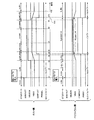
1.4 Aデバイスのステート遷移
図5に、Aデバイスのステート遷移を説明するための図を示す。
【0062】
Aデバイスは、a_idleステートが開始ステートである(ST1)。
【0063】
デュアルロールデバイスのMini−ABレセプタクルに、USBケーブルのMini−Aプラグが挿入されていないとき、プルアップされたID端子は「H」レベル(id)となるため、b_idleステートに遷移する(ST2)。すなわち、デュアルロールデバイスでは、デフォルトでBデバイスとなる。一方、Mini−Aプラグが挿入されると、ID端子が「L」レベル(id/)となるためa_idleステートとなる(ST1)。
【0064】
a_idleステートでは、VBUSへの電流供給が停止される。またデータ信号線D+のプルアップが無効化(オフ)される(プルダウンが有効化される。より具体的には、スイッチ回路SW1がオフ、スイッチ回路SW2がオン)。したがって、ラインステートは「SE0」状態となる。上位アプリケーションからVBUSラインの電圧を落とす要求がないとき(a_bus_drop/)であって、USB転送を行いたいとき(a_bus_req)又はBデバイスからのSRPを検出したとき(a_srp_det)、a_wait_vriseステートに遷移する(ST3)。
【0065】
a_wait_vriseステートでは、VBUSラインへの電流供給が開始され、VBUSラインの電圧が上がる。Mini−Aプラグが抜かれたとき(id)、上位アプリケーションからVBUSラインの電圧を落とす要求があったとき(a_bus_drop)、VBUSラインの電圧が所与の閾値電圧を超えたとき(a_vbus_vld)、又は当該ステートに規定時間以上経過したとき(a_wait_vrise_tmout)、a_wait_bconステートに遷移する(ST4)。
【0066】
a_wait_bconステートでは、Aデバイス側のデータ信号線D+のプルアップがオフとなる。このときBデバイスによりデータ信号線D+のプルアップが有効化(オン)(Bデバイスのスイッチ回路SW3がオン、スイッチ回路SW4がオフ)され、データ信号線D+が「H」レベルになったとき(ラインステートが「J」状態)(b_conn)、a_hostステートに遷移する(ST5)。なお、Mini−Aプラグが抜かれたとき(id)、上位アプリケーションからVBUSラインの電圧を落とす要求があったとき(a_bus_drop)、又は当該ステートで規定時間以上経過したとき(a_wait_bcon_tmout)、a_wait_vfallステートに遷移する(ST6)。また、何らかの原因で、VBUSラインの電圧が所与の閾値電圧を下回ったとき(a_vbus_vld/)、a_vbus_errステートに遷移する(ST7)。
【0067】
すなわちデュアルロールデバイスは、デフォルト状態ではBデバイスであるため、Aデバイスについては、a_wait_bconステートまで、データ信号線D+はプルダウンされた状態のままである。a_wait_vriseステートにおいてVBUSラインへの電流供給が開始されると、Bデバイスのプルアップがオンとなる。これにより、データ信号線D+がプルダウンされた状態であるAデバイスはホストとして動作し、データ信号線D+がプルアップされた状態であるBデバイスはペリフェラルとして動作する。
【0068】
a_hostステートでは、AデバイスがUSB規格のホストとして動作する。より具体的には、ホストとしてペリフェラルをエニュメレート(enumerate)するため、バスリセットするためのリセット信号として、「SE0」状態にデータ信号線を駆動する。そして、所与の規定時間だけその状態を継続させることにより、ペリフェラルではリセット処理が行われる。その後、ホストは、コントロール転送を用いて、コンフィギュレーション情報の転送やアドレスの割り当てなどを行い、USB転送を開始する。当該ステートにおいて、ホストになったがバスを使わなくなったとき(a_bus_req/)、又はサスペンド状態への遷移要求があるとき(a_suspend_req)、a_suspendステートに遷移する(ST8)。また、Mini−Aプラグが抜かれたとき(id)、ラインステートが「J」状態から「SE0」の状態になったとき(b_conn/)、又は上位アプリケーションからVBUSラインの電圧を落とす要求があったとき(a_bus_drop)、a_wait_bconステートに遷移する(ST9)。また、何らかの原因で、VBUSラインの電圧が所与の閾値電圧を下回ったとき(a_vbus_vld/)、a_vbus_errステートに遷移する(ST10)。
【0069】
a_suspendステートでは、SOF(Start Of Frame)パケットの送出が停止される。このとき、Bデバイスはペリフェラルとして動作しており、Bデバイスではb_peripheralステートのままである。このとき、AデバイスがBデバイスに対して上述のHNPを許可し(a_set_b_hnp_en)、Bデバイスにおいてプルアップがオフされてラインステートが「SE0」状態になると(b_conn/)、a_peripheralステートに遷移する(ST11)。また、Aデバイスがバスを使用したいとき(a_bus_req)、又はBデバイスがラインステートを「K」状態にしたとき(b_bus_resume)、a_hostステートに遷移する(ST12)。更にまたAデバイスがBデバイスに対して上述のHNPを許可せず(a_set_b_hnp_en/)、Bデバイスにおいてプルアップがオフされてラインステートが「SE0」状態になると(b_conn/)、a_wait_bconステートに遷移する(ST13)。更にまたMini−Aプラグが抜かれたとき(id)、上位アプリケーションからVBUSラインの電圧を落とす要求があったとき(a_bus_drop)、又はa_suspendステートで規定時間以上経過したとき(a_aidl_bdis_tmout)、a_wait_vfallステートに遷移する(ST14)。また、何らかの原因で、VBUSラインの電圧が所与の閾値電圧を下回ったとき(a_vbus_vld/)、a_vbus_errステートに遷移する(ST15)。
【0070】
a_peripheralステートでは、Aデバイスではプルアップをオンにし、Bデバイスでは後述するようにAデバイスからHNPのイネーブルによりBデバイス側のプルアップがオフされるため、Aデバイスがペリフェラルとなり、Bデバイスがホストになる。ホストとなったBデバイスがデータ転送を終えた場合のようにBデバイスがバスを使わないとき(b_bus_suspend)、a_wait_bconステートに遷移する(ST16)。a_wait_bconステートでは、上述したようにAデバイスのプルアップがオフされる。また、a_peripheralステートにおいて、Mini−Aプラグが抜かれたとき(id)、又は上位アプリケーションからVBUSラインの電圧を落とす要求があったとき(a_bus_drop)、a_wait_vfallステートに遷移する(ST17)。また、何らかの原因で、VBUSラインの電圧が所与の閾値電圧を下回ったとき(a_vbus_vld/)、a_vbus_errステートに遷移する(ST18)。
【0071】
a_bus_errステートでは、過電流状態となるため、例えばファームウェアによりVBUSラインの電圧を落とすように要求される。このようなステートにおいては、Mini−Aプラグが抜かれたとき(id)、又は上位アプリケーションからVBUSラインの電圧を落とす要求があったとき(a_bus_drop)、a_wait_vfallステートに遷移する(ST19)。
【0072】
a_wait_vfallステートでは、VBUSラインへの電流供給が停止される。Mini−Aプラグが抜かれたとき(id)、バスを使いたいとき(a_bus_req)、又はVBUSラインの電圧が所与の閾値電圧を下回った状態で(a_sess_vld/)Bデバイスにおいてプルアップがオフされてラインステートが「SE0」状態になると(b_conn/)、a_idleステートに遷移する(ST20)。
【0073】
1.5 Bデバイスのステート遷移
図6に、Bデバイスのステート遷移を説明するための図を示す。
【0074】
Bデバイスは、b_idleステートが開始ステートである(ST30)。
【0075】
b_idleステートでは、VBUSラインへの電流供給は停止される。したがって、VBUSラインの電圧は、所与の閾値電圧を下回る。またデータ信号線D+のプルアップがオフされる。このとき、Mini−Aプラグが挿入されると、ID端子が「L」レベル(id/)となるためa_idleステートとなる(ST31)。またVBUSラインの電圧が所与の閾値電圧を超えると(b_sess_vld)、b_peripheralステートに遷移する(ST32)。
【0076】
b_peripheralステートでは、データ信号線D+のプルアップがオンとなるため、Aデバイスのa_wait_bconステートにおいてb_connの検出を行うことができる。b_periheralステートでは、Aデバイスからの要求に応答して、ペリフェラルとして動作する。Bデバイスがホストになるときは、Aデバイスがa_suspendになったことを検出し(a_bus_suspend)、Bデバイスの上位アプリケーションからのホスト動作要求(b_bus_req)があって、かつAデバイスからHNPをイネーブルに設定されているとき(b_hnp_en)、b_wait_aconステートに遷移する(ST33)。またb_peripheralステートにおいて、Mini−Aプラグが挿入されたとき(id/)、又はVBUSラインの電圧が所与の閾値電圧を下回ったとき(b_sess_vld/)、b_idleステートに遷移する(ST34)。この結果、b_idleステートにおいてプルアップがオフされ、例えばAデバイスはa_wait_vfallステートからa_idleステートに遷移することができる。
【0077】
b_wait_aconステートでは、Bデバイスのデータ信号線D+のプルアップがオフされ、Aデバイス側でデータ信号線D+がプルアップされるのを待つ。そして、Aデバイス側でデータ信号線D+のプルアップがオンされると(a_conn)、b_hostステートに遷移する(ST35)。またb_wait_aconステートにおいて、Aデバイスがラインステートを「K」状態にしたことを検出したとき(a_bus_resume)、又はb_wait_aconステートで規定時間以上経過すると(b_ase0_brst_tmout)、b_peripheralステートに遷移する(ST36)。また、Mini−Aプラグが挿入されたとき(id/)、又はVBUSラインの電圧が所与の閾値電圧を下回るとき(b_sess_vld/)、b_idleステートに遷移する(ST37)。
【0078】
b_hostステートでは、ホスト処理が行われる。すなわち、バスリセットを行って、SOFパケットの生成を開始する。Aデバイスは、ホストとして動作するBデバイスからの要求に応答することになる。Bデバイスが、ホストとして転送するデータがなくなりバスを使用しないとき(b_bus_req/)、又はAデバイスにおいてプルアップがオフされたことが検出されたとき(a_conn/)、b_peripheralに遷移する(ST38)。このとき、Aデバイスは、Bデバイスのb_bus_suspendとして検出することができ、Aデバイスではa_peripheralステートからa_wait_bconステートに遷移する。この結果、Aデバイスのプルアップがオフされる。b_peripheralステートでは、Bデバイスはプルアップがオンされる。また、b_hostステートにおいて、Mini−Aプラグが挿入されたとき(id/)、又はVBUSラインの電圧が所与の閾値電圧を下回るとき(b_sess_vld/)、b_idleステートに遷移する(ST39)。
【0079】
Bデバイスは、Aデバイスがサスペンド状態のときSRPによりセッション開始を要求することができる。すなわち、b_idleステートにおいて、Bデバイスの上位アプリケーションからのバス使用要求があり(b_bus_req)、VBUSラインの電圧がBデバイスのセッション終了閾値電圧を下回った状態で(b_sess_end)、かつラインステートが「SE0」の状態で規定時間以上経過したとき(b_se0_srp)、b_srp_initステートに遷移する(ST40)。
【0080】
b_srp_initステートでは、SRPによりセッション開始をAデバイスに対して要求する。BデバイスがSRPを終了したとき(b_srp_done)、又はMini−Aプラグが挿入されたとき(id/)、b_idleステートに遷移する(ST41)。
【0081】
2. データ転送制御装置
OTG規格に準拠したデバイスは、上述したSRPをイニシエートする必要性からセルフパワーで動作することが必要となってくる。したがって、当該デバイスが例えばUSB(USB1.1又はUSB2.0)準拠の標準ホストと接続される場合には、標準ホストからVBUSラインに電流が供給されているにも関わらず、自デバイス内の電源を消費するという無駄が生じる。
【0082】
そこで、以下に述べる実施形態におけるOTG規格に準拠したデバイスとしてのデータ転送制御装置は、上述のステート遷移により、デュアルロールデバイスとしての動作を実現する一方、電源切替回路を設け、該電源切替回路により無駄な電力消費を削減することができるようになっている。
【0083】
2.1 第1の実施形態
第1の実施形態におけるデータ転送制御装置は、電源切替回路により、セルフパワー電源からバスパワー電源に切り替えることができる。
【0084】
図7に、第1の実施形態におけるデータ転送制御装置の構成の概要を示す。
【0085】
データ転送制御装置100は、OTGコントローラとしてOTG規格に従ったデータ転送を制御することができる。
【0086】
このようなデータ転送制御装置100は、データ転送処理回路110と、電源回路120と、給電スイッチ回路130と、電源制御回路140と、ID検出回路150と、VBUSコンパレータ160とを含む。
【0087】
データ転送処理回路110は、ステートコントローラ112を含む。ステートコントローラ112は、図5及び図6に示すステート遷移により、Aデバイス(第1のデバイス)のホスト又はペリフェラルとしての動作、Bデバイス(第2のデバイス)のペリフェラル又はホストとしての動作の切り替えを行うことができる。データ転送処理回路110は、ステートコントローラ112のステート遷移により、データ信号線(データライン。D+、D−)を介して、OTG規格に従ったデータ転送の処理を行う。
【0088】
電源回路120は、内部電源切替回路122を含む。内部電源切替回路122は、例えばコンセント等を介して接続される外部電源(AC電源)124、又はデータ転送制御装置100に内蔵する充電式蓄電池126のいずれかから、給電スイッチ回路130を介してVBUSライン、若しくは電源制御回路140を介してデータ転送処理回路110に対して、電源を供給することができるようになっている。
【0089】
給電スイッチ回路130は、ステートコントローラ112において遷移したステートに対応した制御信号VBUSONに基づいて、電源回路120とVBUSラインとを電気的に接続することができる。制御信号VBUSONは、図5に示すAデバイスのa_wait_vriseステート、a_wait_bconステート、a_hostステート、a_suspendステート及びa_peripheralステートのときアクティブになる。また制御信号VBUSONは、図6に示すBデバイスのb_srp_initステートでVBUSパルシングを実施中にアクティブになる。制御信号VBUSONがアクティブのとき、給電スイッチ回路130は電源回路120とVBUSラインとを電気的に接続する。
【0090】
電源制御回路140は、電源切替回路142を含む。電源切替回路142は、切替信号PWRSELにより、VBUSライン又は電源回路120のいずれかと、データ転送処理回路110とを電気的に接続する。すなわち、切替信号PWRSELにより、データ転送処理回路110に対し、VBUSライン又は電源回路120のいずれかから電源が供給される。
【0091】
切替信号PWRSELは、切替スイッチ回路144の出力信号、又はステートコントローラ112からの制御信号に基づいて生成される。ここで切替スイッチ回路144は、例えば機械的にオン・オフを設定可能なスイッチ回路であって、データ転送制御装置100の操作者による手動で切替可能に構成されているものであってもよい。また、ソフトウェア的にオン・オフを設定可能なスイッチ回路であってもよい。また切替信号PWRSELは、切替スイッチ回路144の出力信号とステートコントローラ112からの制御信号とに基づいて生成されるものであってもよい。
【0092】
ID検出回路150は、図2に示すID検出回路12、22と同様にID端子に接続される信号線の電圧を検出し、USBケーブルのプラグの種類を判別するためのものである。
【0093】
VBUSコンパレータ160は、VBUSラインの電圧を監視する。より具体的には、VBUSコンパレータ160は、Aデバイスとして動作時にはVBUSの電圧がAデバイスのセッションバリッド閾値(Session Valid threshold)(Va_sess_vld)やVBUSバリッド閾値(VBUS Valid threshold)(Va_VBUS_vld)を超えたか否かを検出する。またVBUSコンパレータ160は、Bデバイスとして動作時にはVBUSの電圧がBデバイスのセッションバリッド閾値(Vb_sess_vld)を超えたか否かを検出する。ID検出回路150の出力であるID検出信号IDDETECTは、ステートコントローラ112に入力される。VBUSコンパレータ160の出力であるVBUS検出信号VCOMPは、ステートコントローラ112に入力される。
【0094】
図8に、第1の実施形態におけるデータ転送制御装置の電源切替フローの一例を示す。
【0095】
ここでは切替信号が、ステートコントローラ112の出力に基づいて生成される場合を説明する。
【0096】
まず電源が投入されると、データ転送制御装置100は初期化される。そして、ステートコントローラ112では、図5及び図6に示したようにb_idleステートに遷移した状態となる(ステップS200)。これにより、セルフパワー電源、すなわち図7の外部電源124又は充電式蓄電池126からの電源供給により、データ転送制御やその他の回路ブロックが動作する。
【0097】
ここでユーザによってUSBケーブルが接続されると、ID端子に接続される信号線の電圧を検出する(ステップS201)。ID検出回路150により、接続されたUSBケーブルのプラグがMini−Aプラグであることが検出されたとき以外、すなわちID検出信号IDDETECTが「H」のとき(ステップS201:Y)、ステートコントローラ112の出力を判別する(ステップS202)。
【0098】
より具体的には、ステートコントローラ112の出力より、b_idleステート(広義には、Bデバイスのアイドル状態)であり、かつVBUSラインの電圧が「Vb_sess_vld」(第1の閾値)を超えた(b_sess_vldが真)か否かを判別する。これは、データの転送先又は転送元が、USB規格の標準ホスト、或いはOTG規格のAデバイスであって常にVBUSラインに電源を供給するデバイスであるか判別するものである。
【0099】
そして、b_idleステートであり、かつb_sess_vldが真のとき(ステップS202:Y)、バスパワー電源に切り替える(ステップS203)。すなわち電源制御回路140の電源切替回路142により、データ転送処理回路110に対して、VBUSラインから電源を供給するように切り替える。これにより、Bデバイスで動作時においても、データ転送処理回路110はバスパワー電源で動作することになる。
【0100】
その後、電源回路120をディセーブルにして、無駄な電力消費を削減する(ステップS204)。より具体的には、内部電源切替回路122において、外部電源124又は充電式蓄電池126と他の内部回路とを電気的に切断する。
【0101】
なおステップS201でID検出回路150により、接続されたUSBケーブルのプラグがMini−Aプラグであることが検出されたとき(ステップS201:Y)、又はステップS202でb_idleステートかつb_sess_vldが真ではないと判別されたとき(ステップS202:N)、少なくともデータ転送処理回路110はセルフパワー電源により動作することに変化はない。ステップS202で「N」の場合、セルフパワー電源により接続相手に対してSRPをイニシエートすることができる。
【0102】
このように、データ転送制御装置100がセルフパワー電源で動作することが必要とされる場合に、接続相手からVBUSラインに電源が供給されていることが確認されたときに、セルフパワー電源からバスパワー電源に切り替えることができる(内部の電源の供給元を電源回路120からVBUSラインに切り替えることができる)。したがって、接続相手から供給される電源を用いて内部回路を動作させることができるので、内部の電源回路において無駄な電力消費を削減することができる。
【0103】
なお図8ではステートコントローラ112の出力に基づいて切替信号PWRSELを生成するものとして説明したが、切替スイッチ回路144やソフトウェアを用いて切替信号PWRSELを生成するようにしてもよい。
【0104】
2.2 第2の実施形態
第1の実施形態では、電源制御回路140の電源切替回路142によりセルフパワー電源からバスパワー電源に切り替えることができるデータ転送制御装置を提供する。ところが、バスパワー電源に切り替え後、VBUSラインに電源を供給する接続相手が何らかの原因で電源を供給できなくなった場合には、データ転送制御装置は、異常状態としてデータ転送制御を停止せざるを得ない。
【0105】
そこで第2の実施形態では、バスパワー電源に切り替え後にVBUSラインに電源を供給する接続相手が何らかの原因で電源を供給できなくなった場合であっても、バックアップ電源に切り替えて内部回路を正常に動作させ続けることができるようになっている。
【0106】
図9に、第2の実施形態におけるデータ転送制御装置の構成の概要を示す。
【0107】
ここでは第2の実施形態におけるデータ転送制御装置同士が、USBケーブルを介して接続されている状態を示している。すなわち、一方がAデバイスとしてホスト側の電子機器Pに搭載され、他方がBデバイスとしてペリフェラル側の電子機器Qに搭載される。
【0108】
また図7に示した第1の実施形態におけるデータ転送制御装置と同一部分には同一符号を付して適宜説明を省略する。ただし、各符号には、ホスト側のブロックであることを示す「h」、又はペリフェラル側のブロックであることを示す「p」を添えて付している。
【0109】
電子機器P、Qに搭載されるデータ転送制御装置300、400は、同一構成である。図9に示すように、データ転送制御装置300にはMini−Aプラグが接続されているため、データ転送制御装置300はAデバイスとして動作する。データ転送制御装置400にはMini−Bプラグが接続されているため、データ転送制御装置400はBデバイスとして動作する。
【0110】
データ転送制御装置300、400が、第1の実施形態におけるデータ転送制御装置100と異なる点は、電源制御回路340h、340pの構成と、新たに付加されたVBUS電圧検出回路(電源ライン電圧検出回路)350h、350pである。
【0111】
電源制御回路340h、340pは、電源切替回路142h、142pを含む。電源切替回路142hに入力される切替信号PWRSELは、ID検出回路150hと、VBUS電圧検出回路350hの出力信号COMPOUTとの論理積演算結果である。電源切替回路142pに入力される切替信号PWRSELは、ID検出回路150pと、VBUS電圧検出回路350pの出力信号COMPOUTとの論理積演算結果である。
【0112】
VBUS電圧検出回路350h、350pは、VBUSラインの電圧が所与の閾値(第2の閾値)を超えたか否かを検出し、その検出結果を出力信号COMPOUTとして出力する。VBUS電圧検出回路350hにおける閾値(第2の閾値)は、VBUSコンパレータ160hにおける閾値(第1の閾値)より高い。VBUS電圧検出回路350pにおける閾値(第2の閾値)は、VBUSコンパレータ160pにおける閾値(第1の閾値)より高い。
【0113】
図10に、第2の実施形態におけるデータ転送制御装置の電源切替フローの一例を示す。
【0114】
まず電源が投入されると、データ転送制御装置は初期化される。そして、ステートコントローラでは、図5及び図6に示したようにb_idleステートに遷移した状態となる(ステップS450)。これにより、セルフパワー電源、すなわち図10の外部電源124h(124p)又は充電式蓄電池126h(126p)からの電源供給により、データ転送制御やその他の回路ブロックが動作する。
【0115】
ここでユーザによってUSBケーブルが接続されると、ID端子に接続される信号線の電圧を検出する(ステップS451)。ID検出回路150h(150p)により、接続されたUSBケーブルのプラグがMini−Aプラグであることが検出されたとき以外、すなわちID検出信号IDDETECTが「H」のとき(ステップS451:N)、ステートコントローラ112h(112p)の出力を判別する(ステップS452)。
【0116】
より具体的には、ステートコントローラ112h(112p)の出力より、b_idleステート(広義には、Bデバイスのアイドル状態)であり、かつVBUSの電圧が「Vb_sess_vld」(第1の閾値)を超えた(b_sess_vldが真)か否かを判別する。そして、b_idleステートであり、かつb_sess_vldが真のとき(ステップS452:Y)、バスパワー電源に切り替える(ステップS453)。すなわち電源制御回路340h(340p)の電源切替回路142h(142p)により、データ転送処理回路110h(110p)に対して、VBUSラインから電源を供給するように切り替える。
【0117】
その後、電源回路120h(120p)をディセーブルにして、無駄な電力消費を削減する(ステップS454)。より具体的には、内部電源切替回路122h(122p)において、外部電源124h(124p)又は充電式蓄電池126h(126p)と他の内部回路とを電気的に切断する。
【0118】
続いて、状態変数b_backupが偽か否かを判別する(ステップS455)。状態変数b_backupは、VBUSラインの電圧がバックアップ用閾値VB_BACKUP(第2の閾値)を超えたときに真となる。バックアップ用閾値VB_BACKUPは、任意に設定可能な閾値であって、後述するようにBデバイスのセッションバリッド電圧「Vb_sess_vld」(第1の閾値)より高く、AデバイスのVBUSバリッド電圧「Va_VBUS_vld」より低く設定される。状態変数b_backupは、VBUS電圧検出回路350h(350p)の出力信号COMPOUTである。
【0119】
そして、状態変数b_backupが偽になったとき(ステップS455:N)、すなわちVBUSラインの電圧がバックアップ用閾値VB_BACKUP(第2の閾値)を下回ったとき、電源回路120をイネーブルにし(ステップS456)、セルフパワー電源に切り替える(ステップS457)。
【0120】
なおステップS451でID検出回路150h(150p)により、接続されたUSBケーブルのプラグがMini−Aプラグであることが検出されたとき(ステップS451:N)、又はステップS452でb_idleステートかつb_sess_vldが真ではないと判別されたとき(ステップS452:N)、少なくともデータ転送処理回路110はセルフパワー電源により動作することに変化はない。ステップS452で「N」の場合、セルフパワー電源により接続相手に対してSRPをイニシエートすることができる。
【0121】
このように、OTG規格に準拠したデータ転送制御装置において、セルフパワー電源からバスパワー電源に切り替わった後、何らかの原因でVBUSラインに電源が供給されなくなった場合であっても、VBUSラインの電圧降下を検出してセルフパワー電源に切り替えるようにした。これにより、Bデバイスでバスパワー電源に切り替えられた後に、何らかの原因でVBUSラインに電源が供給されなくなっても、セルフパワー電源に切り替えることができるので、内部回路に対し充電式蓄電池等のバックアップ用電源から電源を供給し続けることができる。
【0122】
次に、第2の実施形態におけるデータ転送制御装置の具体的な動作について説明する。
【0123】
図11に、図9に示す第2の実施形態におけるデータ転送制御装置同士が接続された場合の電源切替のタイミングチャートの一例を示す。
【0124】
電源投入後、データ転送制御装置300、400は初期化され、いずれもBデバイスのアイドル状態(b_idleステート)に遷移する。データ転送制御装置300、400は、ともにOTG規格に準拠したデータ転送制御を行うため、デフォルト状態ではセルフパワー電源で動作する。
【0125】
時刻t1において、USBケーブルが接続されるものとする。データ転送制御装置300にMini−Aプラグが接続され、データ転送制御装置400にMini−Bプラグが接続されたものとして考える。
【0126】
データ転送制御装置300のID検出回路150hでは、ID端子に接続された信号線が接地されるため、ID検出信号IDDETECTが「L」となる。したがって、データ転送制御装置300は、USBケーブルの接続が変更されない限り、時刻t1以降ではAデバイスとして動作することになり、a_idleステートに遷移する。すなわち、データ転送制御に関する限り、デフォルト状態ではセルフパワー電源で行われる。一方、データ転送制御装置400のID検出回路150pでは、ID端子がプルアップされたままであるため、ID検出信号IDDETECTが「H」となる。したがって、データ転送制御装置400は、USBケーブルの接続が変更されない限り、時刻t1以降ではBデバイスとして動作することになり、b_idleステートのままとなる。すなわち、データ転送制御に関する限り、デフォルト状態ではバスパワー電源で行われる。
【0127】
そして、データ転送制御装置400において、上位アプリケーションからのバス使用要求等によりSRPをイニシエートするため、時刻t2においてb_srp_initステートに遷移する。このステートでは、データ転送制御装置400は、データ転送制御装置300に対し、SRPをイニシエートする。その結果、データ転送制御装置300がデータ転送制御装置400からのSRPを検出し、時刻t3において、a_wait_vriseステートに遷移する。一方、データ転送制御装置400は、b_srp_done(SRP完了)により、b_idleステートに戻る。
【0128】
データ転送制御装置300では、a_wait_vriseステートにおいて制御信号VBUSONがアクティブになり、給電スイッチ回路130hを介して電源回路120hとVBUSラインとが電気的に接続される。これにより、VBUSラインへの電流供給(電源供給)が開始され、VBUSラインの電圧が上がる。
【0129】
データ転送制御装置400では、VBUSコンパレータ160pにより、VBUSの電圧が監視されている。そして、VBUSコンパレータ160pにより、VBUSの電圧がBデバイスのセッションバリッド閾値(Vb_sess_vld)(第1の閾値)を超えたと判断された時刻t4において、ステートコントローラ112pにおいて、b_peripheralステートに遷移する。データ転送制御装置400は、b_peripheralステートでは、Aデバイスであるデータ転送制御装置300からの要求に応答して、ペリフェラルとして動作する。
【0130】
続く時刻t5では、データ転送制御装置300、400のVBUS電圧検出回路350h、350pにより、VBUSラインの電圧が、Bデバイスのセッションバリッド閾値より高く設定されるバックアップ用閾値VB_BACKUP(第2の閾値)を超えたことが検出される。このとき、VBUS電圧検出回路350h、350pの出力信号COMPOUTが「H」となる。したがって、データ転送制御装置300の電源切替回路142hでは、切替信号PWRSELが「L」のままであるため、電源回路120hとデータ転送処理回路110hとを接続した状態でセルフパワー電源のまま動作する。
【0131】
時刻t6では、Aデバイスとして動作するデータ転送制御装置300において、VBUSコンパレータ160hにより、VBUSラインのAデバイスのVBUSバリッド閾値を超えたことが検出されたとき、a_wait_bconステートに遷移する。
【0132】
データ転送制御装置300は、a_wait_bconステートにおいてデータ転送制御装置400においてデータラインD+がプルアップされたことを時刻t7で確認すると、a_hostステートに遷移する。a_hostステートでは、データ転送制御装置300は、USB規格のホストとして動作する。
【0133】
a_hostステートで、データ転送制御装置300がバスを使用しなくなったとき、又は上位アプリケーションからサスペンド状態への遷移要求があるとき、時刻t8にa_suspendステートに遷移する。
【0134】
ここで、上位アプリケーションからVBUSラインの電圧を落とす要求があったとき、時刻t9において、データ転送制御装置300は、a_wait_vfallステートに遷移する。a_wait_vfallステートでは、VBUSラインへの電流供給が停止され、VBUSラインの電圧が降下する。
【0135】
そして時刻t10において、データ転送制御装置300、400のVBUS電圧検出回路350h、350pにより、VBUSラインの電圧が、バックアップ用閾値VB_BACKUP(第2の閾値)を下回ったことが検出される。このとき、VBUS電圧検出回路350h、350pの出力信号COMPOUTが「L」となる。したがって、データ転送制御装置300の電源切替回路142hでは、切替信号PWRSELが「L」のままであるため、電源回路120hとデータ転送処理回路110hとを接続した状態でセルフパワー電源のまま動作する。一方、データ転送制御装置400の電源切替回路142pでは、切替信号PWRSELが「L」に変化するため、データ転送処理回路110pに対し、電源回路120pから電源が供給されるように切り替えられ、セルフパワー電源で動作することになる。
【0136】
そして、時刻t11において、データ転送制御装置400では、VBUSコンパレータ160pにより、VBUSラインの電圧がBデバイスのセッションバリッド閾値(Vb_sess_vld)(第1の閾値)を下回ったと判断されると、ステートコントローラ112pにおいて、b_idleステートに遷移する。
【0137】
続く時刻t12では、VBUSラインの電圧がBデバイスのセッションバリッド閾値(Vb_sess_vld)(第1の閾値)を下回るため、データ転送制御装置400においてプルアップがオフされてラインステートが「SE0」状態になると、データ転送制御装置300ではa_idleステートに遷移する。
【0138】
このように、Aデバイスとして動作するデータ転送制御装置300はセルフパワー電源のまま動作する。また、Bデバイスとして動作するデータ転送制御装置400は、データ転送制御に関する限りデフォルト状態としてセルフパワー電源として動作するが、VBUSラインを介して電源が供給された状態でペリフェラル動作を行うときにはバスパワー電源で動作することができる。そして、再びVBUSラインを介して電源が供給されなくなったことを検出すると、セルフパワー電源に切り替えて次のデータ転送処理に備える。
【0139】
ところで、Bデバイスに設定されたデータ転送制御装置では、b_idleステートで、VBUSラインの電圧を検出することが望ましい。そのため、セルフパワー電源からバスパワー電源に切り替えるときには、b_idleステートからb_peripheralステートに遷移してから切り替え動作を行うことが望ましい。また、バスパワー電源からセルフパワー電源に切り替えるときには、b_idleステートに遷移する前にセルフパワー電源に切り替えておくことが望ましい。
【0140】
図12に、セルフパワー電源とバスパワー電源の切替時のタイミング図を示す。
【0141】
ここでは、図11に示すタイミング図の該当部分を拡大したものである。第2の実施形態では、バックアップ用閾値VB_BACKUP(第2の閾値)を、Bデバイスのセッションバリッド閾値(Vb_sess_vld。例えば4.0V。)(第1の閾値)より高く、かつAデバイスのVBUSバリッド閾値(Va_VBUS_vld。例えば4.4V)より低い電圧(例えば4.2V)に設定している。
【0142】
こうすることで、Bデバイスでは、VBUSラインの電圧がBデバイスのセッションバリッド閾値(第1の閾値)を超えたことを条件にb_idleステートからb_periheralステートに遷移するため、セルフパワー電源からバスパワー電源への切替をb_peripheralステートで行うことができる。
【0143】
また、Bデバイスでは、VBUSラインの電圧がBデバイスのセッションバリッド閾値(第1の閾値)を下回ったことを条件にb_periheralステートからb_idleステートに遷移するため、バスパワー電源からセルフパワー電源への切替をb_peripheralステートで行うことができる。
【0144】
なおAデバイスでは、VBUSラインの電圧を少なくともAデバイスのVBUSバリッド閾値Va_VBUS_vldまで上げる必要があるため、バックアップ用閾値VB_BACKUPはAデバイスのVBUSバリッド閾値Va_VBUS_vldより低く設定される必要がある。
【0145】
3. 電子機器
次に第1又は第2の実施形態のデータ転送制御装置を含む電子機器の例について説明する。例えば図13(A)に電子機器の1つであるプリンタの内部ブロック図を示し、図14(A)にその外観図を示す。CPU(マイクロコンピュータ)510はシステム全体の制御などを行う。操作部511はプリンタをユーザが操作するためのものである。ROM516には、制御プログラム、フォントなどが格納され、RAM517はCPU510のワーク領域として機能する。DMAC518は、CPU510を介さずにデータ転送を行うためのDMAコントローラである。表示パネル519はプリンタの動作状態をユーザに知らせるためのものである。
【0146】
USBを介してパーソナルコンピュータなどの他のデバイスから送られてきたシリアルの印字データは、データ転送制御装置500によりパラレルの印字データに変換される。そして、変換後のパラレル印字データは、CPU510又はDMAC518により、印字処理部(プリンタエンジン)512に送られる。そして、印字処理部512においてパラレル印字データに対して所与の処理が施され、プリントヘッダなどからなる印字部(データの出力処理を行う装置)514により紙に印字されて出力される。
【0147】
図13(B)に電子機器の1つであるデジタルカメラの内部ブロック図を示し、図14(B)にその外観図を示す。CPU520はシステム全体の制御などを行う。操作部521はデジタルカメラをユーザが操作するためのものである。ROM526には制御プログラムなどが格納され、RAM527はCPU520のワーク領域として機能する。DMAC528はDMAコントローラである。
【0148】
CCDなどからなる撮像部522により撮影対象の画像が読み取られ、読み取られた画像のデータは画像処理部524により処理される。そして、処理後の画像データは、CPU520又はDMAC528によりデータ転送制御装置500に送られる。データ転送制御装置500は、このパラレルの画像データをシリアルデータに変換し、USBを介してパーソナルコンピュータなどの他のデバイスに送信する。
【0149】
図13(C)に電子機器の1つであるCD−RWドライブの内部ブロック図を示し、図14(C)にその外観図を示す。CPU530はシステム全体の制御などを行う。操作部531はCD−RWをユーザが操作するためのものである。ROM536には制御プログラムなどが格納され、RAM537はCPU530のワーク領域として機能する。DMAC538はDMAコントローラである。
【0150】
レーザ、モータ、光学系などからなる読み取り&書き込み部(データの取り込み処理を行う装置又はデータの記憶処理を行うための装置)533によりCD−RW532から読み取られたデータは、信号処理部534に入力され、エラー訂正処理などの所与の信号処理が施される。そして、信号処理が施されたデータが、CPU530又はDMAC538によりデータ転送制御装置500に送られる。データ転送制御装置500は、このパラレルのデータをシリアルデータに変換し、USBを介してパーソナルコンピュータなどの他のデバイスに送信する。
【0151】
一方、USBを介して他のデバイスから送られてきたシリアルのデータは、データ転送制御装置500によりパラレルのデータに変換される。そして、このパラレルデータは、CPU530又はDMAC538により信号処理部534に送られる。そして、信号処理部534においてこのパラレルデータに対して所与の信号処理が施され、読み取り&書き込み部533によりCD−RW532に記憶される。
【0152】
なお、図13(A)、(B)、(C)において、CPU510、520、530の他に、データ転送制御装置500でのデータ転送制御のためのCPUを別に設けるようにしてもよい。
【0153】
上述の実施形態のデータ転送制御装置を電子機器に用いれば、ホスト動作を行うパーソナルコンピュータと接続することなく、USB転送を行うことができる。特に携帯型の電子機器に用いることによって、ユーザはパーソナルコンピュータを持ち歩く必要がなくなり、手軽にUSB転送を行うことができる。例えば、パーソナルコンピュータを介することなく、プリンタや、CD−RWとの間でUSB転送を行うことができる。
【0154】
また上述の実施形態のデータ転送制御装置を電子機器に用いれば、CPU上で動作するファームウェアの処理負荷が軽減され、安価なCPUを用いることが可能になる。更に、データ転送制御装置の低コスト化、小規模化を図れるため、電子機器の低コスト化、小規模化も図れるようになる。
【0155】
なお上述の実施形態のデータ転送制御装置を適用できる電子機器としては、上記以外にも例えば、種々の光ディスクドライブ(CD−ROM、DVD)、光磁気ディスクドライブ(MO)、ハードディスクドライブ、TV、VTR、ビデオカメラ、オーディオ機器、電話機、プロジェクタ、パーソナルコンピュータ、電子手帳、ワードプロセッサなど種々のものを考えることができる。
【0156】
なお、本発明は第1又は第2の実施形態に限定されず、本発明の要旨の範囲内で種々の変形実施が可能である。
【0157】
また、本発明は、OTG規格でのデータ転送に適用されることが特に望ましいが、これに限定されるものではない。例えばOTG規格と同様の思想に基づく規格やOTG規格を発展させた規格におけるデータ転送にも本発明は適用できる。
【0158】
更に上述した実施形態において、転送に先立ってMini−Aプラグが挿入されたデバイスをAデバイス、Mini−Bプラグが挿入されたデバイスをBデバイスであるものとして説明したが、転送制御中に、Aデバイス及びBデバイスを入れ替え、例えばVBUSの供給源を切り替えるようにした場合でも、本発明は適用できる。
【図面の簡単な説明】
【図1】 図1(A)は、Mini−Aプラグ及びMini−Bプラグを有するUSBケーブルの模式図。図1(B)は、Aデバイス及びBデバイスについての説明図。図1(C)は、端子表を示す図。
【図2】USBケーブルが接続されたデュアルロールデバイスの模式例。
【図3】 SRPについての説明図。
【図4】 HNPについての説明図。
【図5】 Aデバイスのステート遷移を説明する図。
【図6】 Bデバイスのステート遷移を説明する図。
【図7】 第1の実施形態におけるデータ転送制御装置の構成ブロック図。
【図8】 第1の実施形態におけるデータ転送制御装置の電源切替フローの一例を示すフロー図。
【図9】 第2の実施形態におけるデータ転送制御装置の構成ブロック図。
【図10】 第2の実施形態におけるデータ転送制御装置の電源切替フローの一例を示すフロー図。
【図11】 図9に示す第2の実施形態におけるデータ転送制御装置同士が接続された場合の電源切替のタイミングチャートの一例のタイミング図。
【図12】 セルフパワー電源とバスパワー電源の切替時のタイミング図。
【図13】 図13(A)〜(C)は電子機器の内部ブロック図。
【図14】 図14(A)〜(C)は電子機器の外観図。
【符号の説明】
100 データ転送制御装置、110 データ転送処理回路、112 ステートコントローラ、120 電源回路、122 内部電源切替回路、124 外部電源、126 充電式蓄電池、130 給電スイッチ回路、140 電源制御回路、142 電源切替回路、144 切替スイッチ回路、160 VBUSコンパレータ[0001]
BACKGROUND OF THE INVENTION
The present invention relates to a data transfer control device, an electronic device, and a power supply switching method.
[0002]
[Background Art and Problems to be Solved by the Invention]
In recent years, the USB (Universal Serial Bus) standard has attracted attention as an interface standard for connecting a personal computer and peripheral devices (electronic devices in a broad sense). However, the USB standard always requires a host, and until now it has not been possible to transfer USB standard data between peripheral devices. Therefore, the “USB On-The-Go (OTG) 1.0” standard (hereinafter abbreviated as OTG standard) is established as an additional standard of the USB 2.0 standard, and USB standard data transfer is also performed between peripheral devices. be able to.
[0003]
In the OTG standard, a peripheral functioning as a device in the USB standard can have a host function necessary for operating as a host. Accordingly, peripheral devices that were devices in the conventional USB standard can be connected to each other, and data transfer can be performed without going through a host in the conventional USB standard.
[0004]
Therefore, in the OTG standard, a dual-role device and a peripheral-only device are defined. A device that becomes a dual-role device can operate as both a host and a peripheral. A device that becomes a peripheral-only device can operate only as a peripheral.
[0005]
By the way, in the OTG standard, in order to reduce power consumption, for example, when a device operating as a host does not use a bus, driving of a power supply line can be stopped. Therefore, for example, when a device that is operating as a peripheral wants to use an unused bus, the bus may be used by a procedure called SRP (Session Request Protocol) that requests the device operating as a host to use the bus. it can. In SRP, a device operating as a peripheral requests a device operating as a host to supply power to the VBUS line by a method called data line pulsing or VBUS (power supply bus) pulsing. As a result, a device compliant with the OTG standard needs to be a self-powered power source in order to initiate the SRP described above.
[0006]
Here, consider a case where a device (OTG device) compliant with the OTG standard is connected to a standard host (for example, a personal computer) compliant with the USB standard. According to the standard, the standard host needs to supply power to the VBUS line. However, since the OTG device is a self-powered power source, the OTG device consumes power from its own power source even though power is always supplied from the standard host to the VBUS line, and is wasteful. There was a problem of consuming a lot of power. In particular, when the OTG device is a portable information device, the battery life is shortened.
[0007]
The present invention has been made in view of the technical problems as described above. The object of the present invention is, for example, data transfer for reducing wasteful power consumption when performing data transfer between peripheral devices of the OTG standard, for example. A control device, an electronic device, and a power supply switching method are provided.
[0008]
[Means for Solving the Problems]
In order to solve the above problems, the present invention provides a state transition of a first device that performs data transfer control with a self-power power source in a default state or a state transition of a second device that performs data transfer control with a bus power power source in a default state Thus, a data transfer control device that controls the switching of the states of the host and peripheral and controls the transfer of data via the data line and the power line, and operates when the power circuit and the first device operate. Based on a given switching signal, either the power supply line or the power supply circuit, a power supply switch circuit for connecting the power supply line and the power supply circuit, a data transfer processing circuit for transferring data via the data line, Power supply switching circuit for supplying power to the data transfer processing circuit from Relating to the data transfer control device comprising and.
[0009]
In the present invention, when operating as the first device, in the data transfer control device that supplies power to the power supply line by the power supply switch circuit, the power supply switching circuit switches the power supply circuit to the power supply line and Power can be supplied. Therefore, for example, when operating as the second device, the data processing circuit can be operated by supplying power from the power supply line, so that power consumption of the power supply circuit can be reduced.
[0010]
The data transfer control device according to the present invention includes a changeover switch circuit that turns on or off the given changeover signal, and the given changeover signal may be generated based on an output of the changeover switch circuit. Good.
[0011]
According to the present invention, the power supply source can be appropriately switched by the changeover switch circuit, so that the power consumption of the data transfer control device can be optimized.
[0012]
The present invention also relates to a data transfer control device for controlling data transfer in accordance with the USB (Universal Serial Bus) OTG (On-The-Go) standard, comprising a power supply circuit, a VBUS line and the power supply when operating as an A device. A power supply switch circuit for connecting a circuit, a data transfer processing circuit for transferring data via a data line, and the data transfer processing circuit from either the VBUS line or the power supply circuit based on a given switching signal A power switching circuit for supplying power to the power supply, wherein the power switching circuit determines that the voltage of the VBUS line has exceeded a first threshold value in an idle state during operation as a B device. , And a data transfer control device that supplies power from the VBUS line to the data transfer processing circuit.
[0013]
A data transfer control device compliant with the OTG standard requires a self-powered power supply. Therefore, for example, even when power is supplied to the VBUS line by a standard host, the data transfer control device consumes power of its own power supply circuit.
[0014]
According to the present invention, the power supply switching circuit can supply power from the power supply line to the data processing circuit and operate with the bus power power supply. Therefore, useless power consumption of the power supply circuit mounted as a self-powered power supply. Can be reduced. Further, since the power supply switching circuit can be operated based on the state transition result, the power supply switching can be optimized without providing a particularly large-scale additional circuit.
[0015]
The present invention also provides a host and peripheral device with a state transition of a first device that performs data transfer control by a self-power power source in a default state or a state transition of a second device that performs data transfer control by a bus power power source in a default state. A data transfer control device that performs state switching control and performs data transfer control via a data line and a power supply line, the power supply circuit, and the power supply line and the power supply circuit when operating as the first device A power supply switch circuit that connects the power line, a data transfer processing circuit that performs data transfer via the data line, a power line voltage detection circuit that detects whether or not the voltage of the power line has exceeded a second threshold, Based on a given switching signal, either the power line or the power circuit A power switching circuit for supplying power to the data transfer processing circuit, the power switching circuit operating as the second device, and the voltage of the power line is lower than the second threshold When it is determined that the first threshold is exceeded, power is supplied from the power line to the data transfer processing circuit, and it is determined that the voltage of the power line does not exceed the second threshold. The data transfer control device for supplying power from the power supply circuit to the data transfer processing circuit.
[0016]
The present invention is also a data transfer control device for controlling data transfer according to the USB (Universal Serial Bus) OTG (On-The-Go) standard, and connects the VBUS line and the power supply circuit when operating as an A device. A power supply switch circuit for performing data transfer, a data transfer processing circuit for performing data transfer via the data line, a power line voltage detecting circuit for detecting whether or not the voltage of the VBUS line exceeds a second threshold, and a given switching A power switching circuit for supplying power to the data transfer processing circuit from either the VBUS line or the power circuit based on a signal, the power switching circuit operating as a B device, and When it is determined that the voltage of the VBUS line exceeds a first threshold value that is lower than the second threshold value, the VBUS line is A data transfer control device for supplying power from the US line and supplying power from the power supply circuit to the data transfer processing circuit when it is determined that the voltage of the VBUS line does not exceed the second threshold value Related to.
[0017]
According to the present invention, after switching from the self-power power supply to the bus power power supply as described above, even if the supply source of the bus power power supply cannot supply power for some reason, the power supply line (VBUS line) Can be switched to the self-powered power source again by the power source switching circuit, and thus the reliability of the data transfer control device that achieves low power consumption by switching the power source can be improved. Further, it is possible to achieve both low consumption and improved reliability of the data transfer control device compliant with the OTG standard.
[0018]
In the data transfer control device according to the present invention, the switching of the power supply source for the data transfer processing circuit from the power supply circuit to the VBUS line is performed after the transition from the idle state of the B device to the peripheral state, Switching of the power supply source to the data transfer processing circuit from the VBUS line to the power supply circuit may be performed before the B device is switched from the peripheral state to the idle state.
[0019]
According to the present invention, since it is only necessary to monitor the voltage of the VBUS line in the idle state of the B device, it is possible to simplify the control by the state management.
[0020]
In the data transfer control device according to the present invention, the second threshold value may be higher than the session valid threshold value of the B device and lower than the VBUS valid threshold value of the A device.
[0021]
According to the present invention, it is possible to monitor the voltage of VBUS in the idle state of the B device only by setting the second threshold value, so that the configuration and control can be simplified.
[0022]
An electronic apparatus according to the present invention includes any one of the data transfer control devices described above, and the data transfer processing device and a device that performs an output process, a capture process, or a storage process of data transferred via a bus. Can do.
[0023]
According to the present invention, it is possible to provide an electronic device that reduces wasteful power consumption by switching to a bus power power source even when a data transfer control device that operates with a self power power source is mounted.
[0024]
The present invention also provides a host and peripheral device with a state transition of a first device that performs data transfer control by a self-power power source in a default state or a state transition of a second device that performs data transfer control by a bus power power source in a default state. A power supply switching method for a data transfer control device that performs state switching control and performs data transfer control via a data line and a power supply line, wherein the data transfer processing circuit performs data transfer via the data line. In the state where power is supplied from the power supply circuit connected to the power supply line during the operation as the first device, the voltage of the power supply line is set to the first threshold value in the idle state during the operation as the second device. And whether or not the second device is in operation. When the idle state voltage of the power line is determined to exceed the first threshold value, related to the power supply switching method for supplying power from the power supply line to the data transfer processing circuit.
[0025]
The present invention is also a power switching method for a data transfer control device that controls data transfer in accordance with the USB (Universal Serial Bus) OTG (On-The-Go) standard, the data being transferred via the data line. When power is supplied from the power supply circuit connected to the VBUS line to the transfer processing circuit when operating as the A device, the voltage of the VBUS line exceeds the first threshold in the idle state when operating as the B device. And when it is determined that the voltage of the VBUS line has exceeded the first threshold value in the idle state during the operation as the B device, a power is supplied from the VBUS line to the data transfer processing circuit. This is related to the power switching method for supplying the power.
[0026]
The present invention also provides a host and peripheral device with a state transition of a first device that performs data transfer control by a self-power power source in a default state or a state transition of a second device that performs data transfer control by a bus power power source in a default state. A power supply switching method for a data transfer control device that performs state switching control and performs data transfer control via a data line and a power supply line, wherein the data transfer processing circuit performs data transfer via the data line. In the state where power is supplied from the power supply circuit connected to the power supply line during the operation as the first device, the voltage of the power supply line is set to the first threshold value in the idle state during the operation as the second device. If the data transfer processing circuit is determined to have exceeded In the state where power is supplied from the power supply line and power is supplied from the power supply line to the data transfer processing circuit, it is determined that the voltage of the power supply line does not exceed a second threshold value. The present invention relates to a power supply switching method for supplying power from the power supply circuit to the transfer processing circuit.
[0027]
The present invention also relates to a power switching method for a data transfer control device that controls data transfer in accordance with USB (Universal Serial Bus) OTG (On-The-Go) standards, and is a data transfer that performs data transfer via a data line. When power is supplied to the processing circuit from the power supply circuit connected to the VBUS line when operating as the A device, the voltage of the VBUS line exceeds the first threshold in the idle state when operating as the B device. When the determination is made, the voltage of the VBUS line is set to a second level when power is supplied from the VBUS line to the data transfer processing circuit and power is supplied from the VBUS line to the data transfer processing circuit. A power supply switching method for supplying power from the power supply circuit to the data transfer processing circuit when it is determined that the threshold value is not exceeded. It engaged to.
[0028]
In the power supply switching method according to the present invention, the switching of the power supply source to the data transfer processing circuit from the power supply circuit to the VBUS line is performed after the transition from the idle state of the B device to the peripheral state, and the VBUS The switching of the power supply source for the data transfer processing circuit from the line to the power supply circuit may be performed before the B device is switched from the peripheral state to the idle state.
[0029]
In the power supply switching method according to the present invention, the first threshold value may be set lower than the second threshold value.
[0030]
In the power supply switching method according to the present invention, the second threshold value may be higher than the session valid threshold value of the B device and lower than the VBUS valid threshold value of the A device.
[0031]
DETAILED DESCRIPTION OF THE INVENTION
DESCRIPTION OF EMBODIMENTS Hereinafter, preferred embodiments of the present invention will be described in detail with reference to the drawings. The embodiments described below do not unduly limit the contents of the present invention described in the claims. Also, not all of the configurations described below are essential constituent requirements of the present invention.
[0032]
1. OTG (On-The-Go) standard
1.1 A device and B device
First, the OTG standard will be briefly described.
[0033]
The USB (Universal Serial Bus) standard is a standard for transferring data between a host (for example, a personal computer) and one or more peripherals (for example, peripheral devices). Transfer control is performed. On the other hand, the amount of data to be processed in portable devices and the like that are peripherals in the USB standard has increased, and there has been an increasing demand for data transfer of the USB standard with low power consumption without interposing a host.
[0034]
Against this background, the OTG standard was formulated as an additional standard for the USB 2.0 standard. The OTG standard newly includes a standard for a dual-role device or the like that allows a peripheral to have a host function necessary for downsizing a connector and operating as a host.
[0035]
When performing data transfer according to the OTG standard, for example, as shown in FIG. 1A, the host and peripheral are connected by a USB cable having Mini-A plugs and Mini-B plugs at both ends. The The Mini-A plug has a structure that can be inserted into a Mini-A receptacle and a Mini-AB receptacle. The Mini-B plug has a structure that can be inserted into the Mini-B receptacle and the Mini-AB receptacle. In the case of a dual roll device, it is necessary to provide a Mini-AB receptacle.
[0036]
By the way, in the USB standard, a host and a peripheral can be connected only by a VBUS (power supply bus) line, GND (ground), and two data signal lines (D +, D−). The VBUS line is supplied with power (electric power, more specifically, power current) from the host side. The data signal lines (data lines) D + and D− are used differentially.
[0037]
In the OTG standard, as shown in FIG. 1B, a dual-role device to which a Mini-A plug is connected is an A device (A-Device) (first device in a broad sense). The A device operates as a host at the start of a session, and can give the host function to the B device under given conditions. On the other hand, the dual role device to which the Mini-B plug is connected is a B device (B-Device) (second device in a broad sense). The B device operates as a peripheral at the start of a session, and is permitted to operate as a host from the A device. The VBUS line is supplied with power by the A device. The A device performs data transfer control by a self-power power supply as a default state. The B device performs data transfer control by the bus power power supply as a default state.
[0038]
In the dual roll device, in order to determine the type of plug inserted into the Mini-AB receptacle, as shown in FIG. 1C, in addition to the conventional connector terminals (VBUS, D−, D +, GND) ID terminals are defined. In the Mini-A plug, the ID terminal is connected to GND, and in the Mini-B plug, the ID terminal is in an open state.
[0039]
FIG. 2 schematically shows an example of a dual roll device to which a USB cable is connected.
[0040]
The dual-
[0041]
Since the dual-
[0042]
Similarly, the
[0043]
In the
[0044]
Since both of the
[0045]
1.2 SRP (Session Request Protocol)
According to the OTG standard, when there is no exchange on the bus, the A device can stop the current supply to the VBUS line. Therefore, even when a portable device or the like that operates on a battery operates as a host, wasteful power consumption can be reduced and low power consumption can be achieved. When the B device starts a session and performs data transfer in this state, it is possible to request the A device to supply current to the VBUS line according to a procedure called SRP. Here, the session means that the VBUS line voltage is a given threshold voltage.BeyondPeriod.
[0046]
FIG. 3 is a diagram for explaining an SRP execution procedure in the FS mode with reference to the configuration of the dual-role device shown in FIG.
[0047]
In the FS mode, the host-side data signal line D + is pulled down (the switch circuit SW1 is turned off and the switch circuit SW2 is turned on), and the peripheral-side data signal line D + is pulled up (the switch circuit SW3 is turned on, the switch circuit SW4 is off).
[0048]
When there is no exchange on the bus and the A device stops supplying the current to the VBUS line (S10), the voltage of VBUS decreases to the “Vb_sess_vld” level (less than B-Device Session Valid) (S11). When detecting this, the B device invalidates the pull-up resistor of the data signal line D + by the switch circuit SW3 (S12). As a result, the line state of the data signal line becomes the “SE0” state (in the FS mode, the data signal line D + is at the “L” level and the data signal line D− is at the “L” level) (S13).
[0049]
When the voltage of VBUS is smaller than “Vb_sess_end” (B-Device Session End) and the “SE0” state of the line state continues for 2 ms or more, the B device can initiate SRP (initiate). SRP can be performed by data-line pulsing or VBUS pulsing. In the data line pulsing, the line states are “SE0” state, “J” state (in the FS mode, the data signal line D + is at “H” level and the data signal line D− is at “L” level), “SE0”. This is a method for transitioning to a state. VBUS pulsing is a method in which a current is supplied from the B device to the VBUS line, and the voltage of the VBUS line is changed to the state of “L” level (less than Vb_sess_end), “H” level (greater than Va_sess_vld), and “L” level. Yes (S14, S15).
[0050]
When the A device monitors the voltage of the data signal line or the VBUS line and detects that the SRP is performed by any method, the A device starts supplying current to the VBUS line (S16). As a result, the voltage of the VBUS line becomes equal to or higher than “Vb_sess_vld” (S17).
[0051]
When the B device detects that the voltage of the VBUS line is equal to or higher than “Vb_sess_end”, the switch circuit SW3 enables the pull-up resistor of the data signal line D + by the switch circuit SW3 (S18), and changes the line state to the “J” state. (S19), and the operation starts as a peripheral.
[0052]
When the device A detects that the line state is in the “J” state, it starts operating as a host (S20).
[0053]
1.3 HNP (Host Negotiation Protocol)
In the OTG standard, the A device or the B device is determined by the connected plug, but the host function and the peripheral function can be exchanged without replacing the plug. The HNP is a procedure for exchanging the host function and the peripheral function.
[0054]
FIG. 4 is a diagram for explaining an HNP execution procedure in the FS mode with reference to the configuration of the dual-role device shown in FIG.
[0055]
Assume that the A device operates as a host, the B device operates as a peripheral, and the HNP is enabled.
[0056]
When the A device finishes using the bus (S30), the line state is set to the idle state (“J” state in the FS mode) (S31).
[0057]
When the B device detects that it is in the “J” state for 3 ms or longer, the switch circuit SW3 disables the pull-up resistor of the data signal line D + (S32), and sets the line state to the “SE0” state (S33). When the device A detects that the line state is the “SE0” state, the switch circuit SW1 enables the pull-up resistor of the data signal line D + (disables the pull-down resistor) (S34). Accordingly, since the line state becomes the “J” state (S35), the A device starts operating as a peripheral, and the B device detects that the line state is “J” and starts operating as a host. (S36).
[0058]
When the B device finishes using the bus as a host (S37), the line state is set to the idle state by the switch circuits SW3 and SW4 (S38). When detecting this, the A device disables the pull-up resistor of the data signal line D + (S39), and changes the line state to the “SE0” state (S40). When the B device detects that the line state is “SE0”, the pull-up resistor of the data signal line D + is made valid (pull-down resistor is made invalid) by the switch circuit SW3 (S41). Thus, since the line state becomes the “J” state (S42), the B device starts operating as a peripheral, and the A device detects that the line state is “J” and starts operating as a host. (S43).
[0059]
Data transfer control according to such a protocol can be realized by transitioning between states that define the respective states according to transition conditions.
[0060]
Hereinafter, state transitions of the A device and the B device will be described.
[0061]
1.4 A device state transition
FIG. 5 is a diagram for explaining the state transition of the A device.
[0062]
In the A device, the a_idle state is the start state (ST1).
[0063]
When the Mini-A plug of the USB cable is not inserted into the Mini-AB receptacle of the dual-role device, the pulled-up ID terminal is at the “H” level (id), and therefore transitions to the b_idle state (ST2). . That is, in the dual role device, the default is the B device. On the other hand, when the Mini-A plug is inserted, since the ID terminal becomes “L” level (id /), the a_idle state is entered (ST1).
[0064]
In the a_idle state, the current supply to VBUS is stopped. Further, the pull-up of the data signal line D + is invalidated (off) (pull-down is validated. More specifically, the switch circuit SW1 is turned off and the switch circuit SW2 is turned on). Therefore, the line state becomes the “SE0” state. When there is no request to drop the voltage of the VBUS line from the upper application (a_bus_drop /), when USB transfer is desired (a_bus_req) or when SRP from the B device is detected (a_srp_det), the state transits to the a_wait_vrise state ( ST3).
[0065]
In the a_wait_vrise state, current supply to the VBUS line is started and the voltage of the VBUS line increases. When the Mini-A plug is removed (id), or when a request to drop the voltage on the VBUS line is received from the upper application (a_bus_drop), the voltage on the VBUS line becomes a given threshold voltage.Beyond(A_vbus_vld), or when a predetermined time or more has passed in the state (a_wait_vrise_tmout), the state transits to the a_wait_bcon state (ST4).
[0066]
In the a_wait_bcon state, the pull-up of the data signal line D + on the A device side is turned off. At this time, the pull-up of the data signal line D + is enabled (ON) by the B device (the switch circuit SW3 of the B device is ON and the switch circuit SW4 is OFF), and the data signal line D + becomes “H” level ( When the line state is “J” state (b_conn), the state transits to the a_host state (ST5). When the Mini-A plug is removed (id), a request to drop the voltage on the VBUS line from the upper application (a_bus_drop), or when a specified time has elapsed in the state (a_wait_bcon_tmout), transition to the a_wait_vfall state (ST6). When the voltage of the VBUS line falls below a given threshold voltage for some reason (a_vbus_vld /), the state transits to the a_vbus_err state (ST7).
[0067]
That is, since the dual-role device is a B device in the default state, the data signal line D + remains pulled down until the a_wait_bcon state for the A device. When current supply to the VBUS line is started in the a_wait_vrise state, the pull-up of the B device is turned on. Thus, the A device in which the data signal line D + is pulled down operates as a host, and the B device in which the data signal line D + is pulled up operates as a peripheral.
[0068]
In the a_host state, the A device operates as a USB standard host. More specifically, the data signal line is driven to the “SE0” state as a reset signal for bus reset in order to enumerate the peripheral as a host. Then, the reset process is performed in the peripheral by continuing the state for a given specified time. Thereafter, the host uses control transfer to transfer configuration information, assign an address, etc., and start USB transfer. In this state, when the host becomes a host but the bus is not used (a_bus_req /) or when there is a request for transition to the suspend state (a_suspend_req), the state transits to the a_suspend state (ST8). Also, when the Mini-A plug is removed (id), when the line state changes from "J" state to "SE0" state (b_conn /), or there is a request from the host application to drop the VBUS line voltage (A_bus_drop), the state transits to the a_wait_bcon state (ST9). When the voltage on the VBUS line falls below a given threshold voltage for some reason (a_vbus_vld /), the state transits to the a_vbus_err state (ST10).
[0069]
In the a_suspend state, transmission of an SOF (Start Of Frame) packet is stopped. At this time, the B device operates as a peripheral, and the B device remains in the b_peripheral state. At this time, the A device permits the above-described HNP to the B device (a_set_b_hnp_en), and when the pull-up is turned off in the B device and the line state becomes the “SE0” state (b_conn /), the device transits to the a_peripheral state ( ST11). Further, when the A device wants to use the bus (a_bus_req) or the B device changes the line state to the “K” state (b_bus_resume), the device transits to the a_host state (ST12). Furthermore, when the A device does not allow the above-described HNP to the B device (a_set_b_hnp_en /) and the pull-up is turned off at the B device and the line state becomes the “SE0” state (b_conn /), the device transits to the a_wait_bcon state. (ST13). Furthermore, when the Mini-A plug is removed (id), a request to drop the voltage of the VBUS line from the upper application (a_bus_drop), or when a specified time has passed in the a_suspend state (a_aidl_bdis_tmout), transition to the a_wait_vfall state (ST14). When the voltage on the VBUS line falls below a given threshold voltage for some reason (a_vbus_vld /), the state transits to the a_vbus_err state (ST15).
[0070]
In the a_peripheral state, the pull-up is turned on in the A device, and in the B device, the pull-up on the B device side is turned off by enabling HNP from the A device as described later, so that the A device becomes a peripheral and the B device becomes a host. Become. When the B device does not use the bus (b_bus_suspend) as in the case where the B device serving as the host finishes data transfer, the device transits to the a_wait_bcon state (ST16). In the a_wait_bcon state, the pull-up of the A device is turned off as described above. In the a_peripheral state, when the Mini-A plug is removed (id), or when there is a request to drop the voltage on the VBUS line from the upper application (a_bus_drop), the state transits to the a_wait_vfall state (ST17). When the voltage on the VBUS line falls below a given threshold voltage for some reason (a_vbus_vld /), the state transits to the a_vbus_err state (ST18).
[0071]
Since the a_bus_err state is an overcurrent state, the firmware requests that the voltage of the VBUS line be lowered, for example. In such a state, when the Mini-A plug is removed (id), or when there is a request to drop the voltage of the VBUS line from the upper application (a_bus_drop), the state transits to the a_wait_vfall state (ST19).
[0072]
In the a_wait_vfall state, the current supply to the VBUS line is stopped. When the Mini-A plug is unplugged (id), when you want to use the bus (a_bus_req), or when the VBUS line voltage is below a given threshold voltage (a_sess_vld /) the pull-up is turned off in the B device When the line state becomes the “SE0” state (b_conn /), the state transits to the a_idle state (ST20).
[0073]
1.5 State transition of B device
FIG. 6 is a diagram for explaining the state transition of the B device.
[0074]
In the B device, the b_idle state is the start state (ST30).
[0075]
In the b_idle state, the current supply to the VBUS line is stopped. Thus, the voltage on the VBUS line is below a given threshold voltage. Further, the pull-up of the data signal line D + is turned off. At this time, when the Mini-A plug is inserted, since the ID terminal becomes “L” level (id /), the a_idle state is entered (ST31). Also, the voltage on the VBUS line gives a given threshold voltageBeyondThen (b_sess_vld), the state transits to the b_peripheral state (ST32).
[0076]
In the b_peripheral state, since the pull-up of the data signal line D + is turned on, b_conn can be detected in the a_wait_bcon state of the A device. In the b_peripheral state, it operates as a peripheral in response to a request from the A device. When the B device becomes a host, it detects that the A device has become a_suspend (a_bus_suspend), and there is a host operation request (b_bus_req) from the upper application of the B device, and the H device enables HNP. When it is set (b_hnp_en), the state transits to the b_wait_acon state (ST33). In the b_peripheral state, when the Mini-A plug is inserted (id /), or when the voltage on the VBUS line falls below a given threshold voltage (b_sess_vld /), the state transits to the b_idle state (ST34). As a result, the pull-up is turned off in the b_idle state, and for example, the A device can transition from the a_wait_vfall state to the a_idle state.
[0077]
In the b_wait_acon state, the pull-up of the data signal line D + of the B device is turned off, and it waits for the data signal line D + to be pulled up on the A device side. When the pull-up of the data signal line D + is turned on on the A device side (a_conn), the device transits to the b_host state (ST35). In the b_wait_acon state, when the device A detects that the line state is set to the “K” state (a_bus_resume), or when the specified time elapses in the b_wait_acon state (b_ase0_brst_tmout), the device transits to the b_peripheral state (ST36). Further, when the Mini-A plug is inserted (id /), or when the voltage of the VBUS line falls below a given threshold voltage (b_sess_vld /), the state transits to the b_idle state (ST37).
[0078]
In the b_host state, host processing is performed. That is, a bus reset is performed and generation of an SOF packet is started. The A device responds to a request from the B device operating as a host. When the B device runs out of data to be transferred as a host and does not use the bus (b_bus_req /), or when it is detected that the pull-up is turned off in the A device (a_conn /), the B device transits to b_peripheral (ST38). At this time, the A device can be detected as b_bus_suspend of the B device, and the A device transits from the a_peripheral state to the a_wait_bcon state. As a result, the pull-up of the A device is turned off. In the b_peripheral state, pull-up is turned on for the B device. In the b_host state, when the Mini-A plug is inserted (id /), or when the voltage of the VBUS line is lower than a given threshold voltage (b_sess_vld /), the state transits to the b_idle state (ST39).
[0079]
The B device can request a session start by SRP when the A device is in the suspended state. That is, in the b_idle state, there is a bus use request from an upper application of the B device (b_bus_req), the voltage of the VBUS line is lower than the session end threshold voltage of the B device (b_sess_end), and the line state is “SE0”. When a specified time or more has elapsed in this state (b_se0_srp), the state transits to the b_srp_init state (ST40).
[0080]
In the b_srp_init state, the A device is requested to start a session by SRP. When the B device finishes the SRP (b_srp_done), or when the Mini-A plug is inserted (id /), the device transits to the b_idle state (ST41).
[0081]
2. Data transfer control device
A device compliant with the OTG standard is required to operate with self-power because of the need to initiate the SRP described above. Therefore, when the device is connected to a standard host conforming to USB (USB 1.1 or USB 2.0), for example, the power supply in the device itself is supplied even though current is supplied from the standard host to the VBUS line. Waste of consumption occurs.
[0082]
Therefore, the data transfer control device as a device compliant with the OTG standard in the embodiment described below realizes an operation as a dual-role device by the state transition described above, while providing a power supply switching circuit. Wasteful power consumption can be reduced.
[0083]
2.1 First embodiment
The data transfer control device in the first embodiment can be switched from the self-power power supply to the bus power power supply by the power supply switching circuit.
[0084]
FIG. 7 shows an outline of the configuration of the data transfer control device in the first embodiment.
[0085]
The data
[0086]
Such a data
[0087]
The data
[0088]
The
[0089]
The power
[0090]
The power
[0091]
The switching signal PWRSEL is generated based on the output signal of the
[0092]
Similar to the
[0093]
The
[0094]
FIG. 8 shows an example of a power supply switching flow of the data transfer control device in the first embodiment.
[0095]
Here, a case where the switching signal is generated based on the output of the
[0096]
First, when the power is turned on, the data
[0097]
Here, when the USB cable is connected by the user, the voltage of the signal line connected to the ID terminal is detected (step S201). When the
[0098]
More specifically, from the output of the
[0099]
When it is in the b_idle state and b_sess_vld is true (step S202: Y), it switches to the bus power supply (step S203). That is, the
[0100]
Thereafter, the
[0101]
When the
[0102]
As described above, when it is necessary for the data
[0103]
Although FIG. 8 has been described as generating the switching signal PWRSEL based on the output of the
[0104]
2.2 Second Embodiment
The first embodiment provides a data transfer control device that can switch from a self-powered power supply to a bus-powered power supply by the power
[0105]
Therefore, in the second embodiment, even if the connection partner that supplies power to the VBUS line after switching to the bus power power supply cannot supply power for some reason, the internal circuit operates normally by switching to the backup power supply. You can continue to let me.
[0106]
FIG. 9 shows an outline of the configuration of the data transfer control device according to the second embodiment.
[0107]
Here, a state is shown in which the data transfer control devices in the second embodiment are connected via a USB cable. That is, one is mounted on the host-side electronic device P as the A device, and the other is mounted on the peripheral-side electronic device Q as the B device.
[0108]
Also, the same parts as those of the data transfer control device in the first embodiment shown in FIG. However, “h” indicating a block on the host side or “p” indicating a block on the peripheral side is attached to each code.
[0109]
The data
[0110]
The data
[0111]
The power
[0112]
The VBUS voltage detection circuits 350h and 350p detect whether or not the voltage of the VBUS line has exceeded a given threshold value (second threshold value), and output the detection result as an output signal COMPOUT. The threshold value (second threshold value) in the VBUS voltage detection circuit 350h is higher than the threshold value (first threshold value) in the
[0113]
FIG. 10 shows an example of a power supply switching flow of the data transfer control device in the second embodiment.
[0114]
First, when the power is turned on, the data transfer control device is initialized. Then, the state controller enters the b_idle state as shown in FIGS. 5 and 6 (step S450). Thereby, the data transfer control and other circuit blocks are operated by the power supply from the self-power source, that is, the external power source 124h (124p) or the
[0115]
Here, when the USB cable is connected by the user, the voltage of the signal line connected to the ID terminal is detected (step S451). When the ID detection circuit 150h (150p) detects that the plug of the connected USB cable is a Mini-A plug, that is, when the ID detection signal IDDETECT is “H” (step S451: N), the state The output of the controller 112h (112p) is determined (step S452).
[0116]
More specifically, from the output of the state controller 112h (112p), the state is the b_idle state (in a broad sense, the idle state of the B device), and the voltage of VBUS exceeds “Vb_sess_vld” (first threshold) ( It is determined whether or not b_sess_vld is true. When it is in the b_idle state and b_sess_vld is true (step S452: Y), it switches to the bus power supply (step S453). That is, the power
[0117]
Thereafter, the
[0118]
Subsequently, it is determined whether or not the state variable b_backup is false (step S455). The state variable b_backup indicates that the VBUS line voltage is the backup threshold VB_BACKUPTrue when (second threshold) is exceeded. Backup threshold VB_BACKUPIs a threshold that can be arbitrarily set, and is set higher than the session valid voltage “Vb_sess_vld” (first threshold) of the B device and lower than the VBUS valid voltage “Va_VBUS_vld” of the A device, as will be described later. The state variable b_backup is the output signal COMPOUT of the VBUS voltage detection circuit 350h (350p).
[0119]
When the state variable b_backup becomes false (step S455: N), that is, the voltage of the VBUS line is the backup threshold V.B_BACKUPWhen the value falls below (second threshold value), the
[0120]
In step S451, when the ID detection circuit 150h (150p) detects that the connected USB cable plug is a Mini-A plug (step S451: N), or in step S452, the b_idle state and b_sess_vld are true. When it is determined that it is not (step S452: N), there is no change in that at least the data
[0121]
As described above, in the data transfer control device compliant with the OTG standard, the voltage drop of the VBUS line even when the power is not supplied to the VBUS line for some reason after switching from the self-power power supply to the bus power power supply. Was detected and switched to a self-powered power supply. As a result, even if power is not supplied to the VBUS line for some reason after switching to the bus power power supply at the B device, it can be switched to the self-power power supply, so the internal circuit can be used for backup of rechargeable storage batteries, etc. Power can be continuously supplied from the power source.
[0122]
Next, a specific operation of the data transfer control device in the second embodiment will be described.
[0123]
FIG. 11 shows an example of a power supply switching timing chart when the data transfer control devices in the second embodiment shown in FIG. 9 are connected to each other.
[0124]
After the power is turned on, the data
[0125]
It is assumed that the USB cable is connected at time t1. Assume that the Mini-A plug is connected to the data
[0126]
In the ID detection circuit 150h of the data
[0127]
Then, the data
[0128]
In the data
[0129]
In the data
[0130]
At subsequent time t5, the VBUS voltage detection circuits 350h and 350p of the data
[0131]
At time t6, in the data
[0132]
When the data
[0133]
When the data
[0134]
Here, when there is a request from the upper application to drop the voltage on the VBUS line, the data
[0135]
At time t10, the VBUS voltage detection circuits 350h and 350p of the data
[0136]
At time t11, in the data
[0137]
At subsequent time t12, since the voltage of the VBUS line falls below the session valid threshold (Vb_sess_vld) (first threshold) of the B device, the pull-up is turned off in the data
[0138]
Thus, the data
[0139]
By the way, in the data transfer control device set in the B device, it is desirable to detect the voltage of the VBUS line in the b_idle state. Therefore, when switching from the self power power supply to the bus power power supply, it is desirable to perform the switching operation after transitioning from the b_idle state to the b_peripheral state. When switching from the bus power supply to the self-power supply, it is desirable to switch to the self-power supply before transitioning to the b_idle state.
[0140]
FIG. 12 is a timing chart at the time of switching between the self-power power source and the bus power power source.
[0141]
Here, the relevant part of the timing diagram shown in FIG. 11 is enlarged. In the second embodiment, the backup threshold VB_BACKUP(Second threshold) is higher than the B device session valid threshold (Vb_sess_vld, for example 4.0 V) (first threshold) and lower than the A device VBUS valid threshold (Va_VBUS_vld, for example 4.4 V). (For example, 4.2V).
[0142]
By doing so, the B device transitions from the b_idle state to the b_peripheral state on condition that the voltage of the VBUS line exceeds the session valid threshold (first threshold) of the B device. Can be switched in the b_peripheral state.
[0143]
In the B device, the transition from the b_peripheral state to the b_idle state is performed on the condition that the voltage of the VBUS line is lower than the session valid threshold (first threshold) of the B device. Can be performed in the b_peripheral state.
[0144]
In the A device, it is necessary to raise the voltage of the VBUS line to at least the VBUS valid threshold Va_VBUS_vld of the A device.B_BACKUPNeeds to be set lower than the VBUS valid threshold Va_VBUS_vld of the A device.
[0145]
3. Electronics
Next, an example of an electronic device including the data transfer control device of the first or second embodiment will be described. For example, FIG. 13A shows an internal block diagram of a printer which is one of electronic devices, and FIG. 14A shows an external view thereof. A CPU (microcomputer) 510 controls the entire system. An
[0146]
Serial print data sent from another device such as a personal computer via USB is converted into parallel print data by the data
[0147]
FIG. 13B shows an internal block diagram of a digital camera which is one of electronic devices, and FIG. 14B shows an external view thereof. The
[0148]
An image to be photographed is read by an
[0149]
FIG. 13C shows an internal block diagram of a CD-RW drive which is one of electronic devices, and FIG. 14C shows an external view thereof. The
[0150]
Data read from the CD-
[0151]
On the other hand, serial data sent from another device via the USB is converted into parallel data by the data
[0152]
13A, 13B, and 13C, in addition to the
[0153]
If the data transfer control device of the above-described embodiment is used in an electronic device, USB transfer can be performed without being connected to a personal computer that performs a host operation. In particular, by using it in a portable electronic device, the user does not need to carry a personal computer and can easily perform USB transfer. For example, USB transfer can be performed between a printer and a CD-RW without using a personal computer.
[0154]
Further, if the data transfer control device of the above-described embodiment is used in an electronic device, the processing load of firmware operating on the CPU is reduced, and an inexpensive CPU can be used. Furthermore, since the cost and scale of the data transfer control device can be reduced, the cost and scale of the electronic device can be reduced.
[0155]
The electronic apparatus to which the data transfer control device of the above-described embodiment can be applied includes, for example, various optical disk drives (CD-ROM, DVD), magneto-optical disk drives (MO), hard disk drives, TVs, VTRs. Various devices such as a video camera, an audio device, a telephone, a projector, a personal computer, an electronic notebook, and a word processor can be considered.
[0156]
The present invention is not limited to the first or second embodiment, and various modifications can be made within the scope of the gist of the present invention.
[0157]
The present invention is particularly preferably applied to data transfer according to the OTG standard, but is not limited to this. For example, the present invention can be applied to data transfer in a standard based on the same idea as the OTG standard or a standard developed from the OTG standard.
[0158]
Further, in the above-described embodiment, it has been described that the device in which the Mini-A plug is inserted prior to the transfer is the A device and the device in which the Mini-B plug is inserted is the B device. The present invention can be applied even when the device and the B device are exchanged, for example, the VBUS supply source is switched.
[Brief description of the drawings]
FIG. 1A is a schematic diagram of a USB cable having a Mini-A plug and a Mini-B plug. FIG. 1B is an explanatory diagram of the A device and the B device. FIG. 1C illustrates a terminal table.
FIG. 2 is a schematic example of a dual roll device to which a USB cable is connected.
FIG. 3 is an explanatory diagram of SRP.
FIG. 4 is an explanatory diagram of HNP.
FIG. 5 is a diagram for explaining state transition of an A device.
FIG. 6 is a diagram for explaining a state transition of a B device.
FIG. 7 is a configuration block diagram of a data transfer control device according to the first embodiment.
FIG. 8 is a flowchart showing an example of a power supply switching flow of the data transfer control device according to the first embodiment.
FIG. 9 is a configuration block diagram of a data transfer control device according to a second embodiment.
FIG. 10 is a flowchart showing an example of a power supply switching flow of the data transfer control device according to the second embodiment.
FIG. 11 is a timing chart showing an example of a power supply switching timing chart when the data transfer control devices in the second embodiment shown in FIG. 9 are connected to each other.
FIG. 12 is a timing chart at the time of switching between the self-power supply and the bus power supply.
FIGS. 13A to 13C are internal block diagrams of electronic devices.
14A to 14C are external views of electronic devices.
[Explanation of symbols]
DESCRIPTION OF
Claims (9)
電源回路と、
Aデバイスとしての動作時にVBUSラインと前記電源回路とを接続する給電スイッチ回路と、
データラインを介してデータ転送を行うデータ転送処理回路と、
所与の切替信号に基づいて、前記VBUSライン又は前記電源回路のいずれかから前記データ転送処理回路に対して電源を供給するための電源切替回路と、
を含み、
前記データ転送制御装置は、Bデバイスとしての動作時に、前記VBUSラインへの電流供給が停止されるアイドル状態において前記VBUSラインの電圧がBデバイスのセッションを開始するための第1の閾値を超えたか否かを判断することで前記データラインを介して接続されたデバイスが前記VBUSラインに電源を供給するか否かを判別し、
前記データラインを介して接続されたデバイスが前記VBUSラインに電源を供給すると判別された場合に、前記電源切替回路は、前記データ転送処理回路に対して前記VBUSラインから電源を供給することを特徴とするデータ転送制御装置。A data transfer control device for controlling data transfer in accordance with a USB (Universal Serial Bus) OTG (On-The-Go) standard,
A power circuit;
A power supply switch circuit for connecting the VBUS line and the power supply circuit when operating as an A device;
A data transfer processing circuit for transferring data via the data line;
A power switching circuit for supplying power to the data transfer processing circuit from either the VBUS line or the power circuit based on a given switching signal;
Including
The data transfer control device, when operating as a B-device, or the voltage of the VBUS line in idle current supply is stopped to the VBUS line exceeds a first threshold value for starting a session B device Determining whether or not a device connected via the data line supplies power to the VBUS line;
When it is determined that a device connected through the data line supplies power to the VBUS line, the power switching circuit supplies power from the VBUS line to the data transfer processing circuit. A data transfer control device.
電源回路と、
Aデバイスとしての動作時にVBUSラインと前記電源回路とを接続する給電スイッチ回路と、
データラインを介してデータ転送を行うデータ転送処理回路と、
前記VBUSラインの電圧が第2の閾値を超えたか否かを検出する電源ライン電圧検出回路と、
所与の切替信号に基づいて、前記VBUSライン又は前記電源回路のいずれかから前記データ転送処理回路に対して電源を供給するための電源切替回路と、
を含み、
前記データ転送制御装置は、
Bデバイスとしての動作時に、前記VBUSラインへの電流供給が停止されるアイドル状態において前記VBUSラインの電圧が前記第2の閾値より低くBデバイスのセッションを開始するための第1の閾値を超えたか否かを判断することで前記データラインを介して接続されたデバイスが前記VBUSラインに電源を供給するか否かを判別し、
前記電源切替回路は、
前記データラインを介して接続されたデバイスが前記VBUSラインに電源を供給すると判別された場合に、前記データ転送処理回路に対して前記VBUSラインから電源を供給し、
前記VBUSラインの電圧が前記第2の閾値を超えた後前記VBUSラインの電圧が降下して前記第2の閾値を超えていないと判断された場合に、前記データ転送処理回路に対して前記電源回路から電源を供給することを特徴とするデータ転送制御装置。A data transfer control device for controlling data transfer in accordance with a USB (Universal Serial Bus) OTG (On-The-Go) standard,
A power circuit;
A power supply switch circuit for connecting the VBUS line and the power supply circuit when operating as an A device;
A data transfer processing circuit for transferring data via the data line;
A power supply line voltage detection circuit for detecting whether the voltage of the VBUS line exceeds a second threshold;
A power switching circuit for supplying power to the data transfer processing circuit from either the VBUS line or the power circuit based on a given switching signal;
Including
The data transfer control device includes:
When operating as a B device, whether the voltage on the VBUS line is lower than the second threshold and exceeds a first threshold for initiating a B device session in an idle state where current supply to the VBUS line is stopped Determining whether or not a device connected via the data line supplies power to the VBUS line;
The power switching circuit is
When it is determined that a device connected via the data line supplies power to the VBUS line, power is supplied from the VBUS line to the data transfer processing circuit.
When it is determined that the voltage of the VBUS line has dropped and has not exceeded the second threshold after the voltage of the VBUS line has exceeded the second threshold, the power supply to the data transfer processing circuit A data transfer control device for supplying power from a circuit.
前記第2の閾値は、
AデバイスのVBUSバリッド電圧より低い電圧であることを特徴とするデータ転送制御装置。In claim 2,
The second threshold is:
A data transfer control device, wherein the voltage is lower than the VBUS valid voltage of the A device.
前記電源回路から前記VBUSラインへの前記データ転送処理回路に対する電源の供給元の切り替えは、Bデバイスのアイドル状態からペリフェラル状態に遷移した後に行われ、
前記VBUSラインから前記電源回路への前記データ転送処理回路に対する電源の供給元の切り替えは、Bデバイスのペリフェラル状態からアイドル状態に切り替わる前に行われることを特徴とするデータ転送制御装置。In claim 2 or 3,
Switching of the power supply source to the data transfer processing circuit from the power supply circuit to the VBUS line is performed after transition from the idle state of the B device to the peripheral state,
The data transfer control device according to claim 1, wherein switching of a power supply source to the data transfer processing circuit from the VBUS line to the power supply circuit is performed before the B device is switched from the peripheral state to the idle state.
前記データ転送処理装置及びバスを介して転送されるデータの出力処理又は取り込み処理又は記憶処理を行う装置と、
を含むことを特徴とする電子機器。A data transfer control device according to any one of claims 1 to 4,
An apparatus for performing an output process or a capture process or a storage process of the data transferred via the data transfer processing device and the bus;
An electronic device comprising:
データラインを介してデータ転送を行うデータ転送処理回路に対し、Aデバイスとしての動作時にVBUSラインに接続される電源回路から電源を供給した状態で、Bデバイスとして動作時に、前記VBUSラインへの電流供給が停止されるアイドル状態において前記VBUSラインの電圧がBデバイスがセッションを開始するための第1の閾値を超えたか否かを判断することで前記データラインを介して接続されたデバイスが前記VBUSラインに電源を供給するか否かを判別し、
前記データラインを介して接続されたデバイスが前記VBUSラインに電源を供給すると判別された場合に、前記データ転送処理回路に対して前記VBUSラインから電源を供給することを特徴とする電源切替方法。A power switching method for a data transfer control device for controlling data transfer in accordance with a USB (Universal Serial Bus) OTG (On-The-Go) standard,
A current to the VBUS line when operating as a B device while power is supplied from a power supply circuit connected to the VBUS line during operation as an A device to a data transfer processing circuit that performs data transfer via the data line A device connected via the data line determines whether the voltage of the VBUS line exceeds a first threshold for the B device to start a session in an idle state where supply is stopped. Determine whether to supply power to the line,
A power supply switching method comprising: supplying power from the VBUS line to the data transfer processing circuit when it is determined that a device connected via the data line supplies power to the VBUS line.
データラインを介してデータ転送を行うデータ転送処理回路に対し、Aデバイスとしての動作時にVBUSラインに接続される電源回路から電源を供給した状態で、Bデバイスとしての動作時に、前記VBUSラインへの電流供給が停止されるアイドル状態において前記VBUSラインの電圧が第2の閾値より低くBデバイスのセッションを開始するための第1の閾値を超えたか否かを判断することで前記データラインを介して接続されたデバイスが前記VBUSラインに電源を供給するか否かを判別し、
前記データラインを介して接続されたデバイスが前記VBUSラインに電源を供給すると判別された場合に、前記データ転送処理回路に対して前記VBUSラインから電源を供給し、
前記データ転送処理回路に対し前記VBUSラインから電源を供給した状態で、前記VBUSラインの電圧が前記第2の閾値を越えた後前記VBUSラインの電圧が降下して前記第2の閾値を超えないと判断された場合に、前記データ転送処理回路に対して前記電源回路から電源を供給することを特徴とする電源切替方法。A power switching method for a data transfer control device for controlling data transfer in accordance with a USB (Universal Serial Bus) OTG (On-The-Go) standard,
In a state where power is supplied from a power supply circuit connected to the VBUS line during operation as the A device, a data transfer processing circuit that performs data transfer via the data line is supplied to the VBUS line during operation as the B device. Via the data line by determining whether the voltage on the VBUS line is lower than a second threshold and exceeds a first threshold for initiating a B device session in an idle state where current supply is stopped. Determining whether the connected device supplies power to the VBUS line;
When it is determined that a device connected via the data line supplies power to the VBUS line, power is supplied from the VBUS line to the data transfer processing circuit.
In a state where power is supplied from the VBUS line to the data transfer processing circuit, the voltage on the VBUS line drops and does not exceed the second threshold after the voltage on the VBUS line exceeds the second threshold. When it is determined that the power is switched, the power supply circuit supplies power to the data transfer processing circuit from the power supply circuit.
前記第2の閾値は、
AデバイスのVBUSバリッド電圧より低い電圧であることを特徴とする電源切替方法。In claim 7,
The second threshold is:
A power supply switching method, wherein the voltage is lower than the VBUS valid voltage of the A device.
前記電源回路から前記VBUSラインへの前記データ転送処理回路に対する電源の供給元の切り替えは、Bデバイスのアイドル状態からペリフェラル状態に遷移した後に行われ、
前記VBUSラインから前記電源回路への前記データ転送処理回路に対する電源の供給元の切り替えは、Bデバイスのペリフェラル状態からアイドル状態に切り替わる前に行われることを特徴とする電源切替方法。In claim 7 or 8,
Switching of the power supply source to the data transfer processing circuit from the power supply circuit to the VBUS line is performed after transition from the idle state of the B device to the peripheral state,
Switching the power supply source for the data transfer processing circuit from the VBUS line to the power supply circuit is performed before the B device is switched from the peripheral state to the idle state.
Priority Applications (2)
| Application Number | Priority Date | Filing Date | Title |
|---|---|---|---|
| JP2002253382A JP3654274B2 (en) | 2002-08-30 | 2002-08-30 | Data transfer control device, electronic device, and power supply switching method |
| US10/379,592 US6963933B2 (en) | 2002-08-30 | 2003-03-06 | Data transfer control device, electronic equipment, and power supply switching method |
Applications Claiming Priority (1)
| Application Number | Priority Date | Filing Date | Title |
|---|---|---|---|
| JP2002253382A JP3654274B2 (en) | 2002-08-30 | 2002-08-30 | Data transfer control device, electronic device, and power supply switching method |
Related Child Applications (1)
| Application Number | Title | Priority Date | Filing Date |
|---|---|---|---|
| JP2003085980A Division JP2004094914A (en) | 2003-03-26 | 2003-03-26 | Data transfer control device, electronic equipment and power supply switching method |
Publications (2)
| Publication Number | Publication Date |
|---|---|
| JP2004094495A JP2004094495A (en) | 2004-03-25 |
| JP3654274B2 true JP3654274B2 (en) | 2005-06-02 |
Family
ID=31972793
Family Applications (1)
| Application Number | Title | Priority Date | Filing Date |
|---|---|---|---|
| JP2002253382A Expired - Fee Related JP3654274B2 (en) | 2002-08-30 | 2002-08-30 | Data transfer control device, electronic device, and power supply switching method |
Country Status (2)
| Country | Link |
|---|---|
| US (1) | US6963933B2 (en) |
| JP (1) | JP3654274B2 (en) |
Families Citing this family (66)
| Publication number | Priority date | Publication date | Assignee | Title |
|---|---|---|---|---|
| US7791319B2 (en) * | 2003-02-21 | 2010-09-07 | Research In Motion Limited | Circuit and method of operation for an electrical power supply |
| JP2004310672A (en) * | 2003-04-10 | 2004-11-04 | Seiko Epson Corp | Data input device and image output system |
| GB2402271B (en) * | 2003-05-27 | 2006-04-19 | Research In Motion Ltd | Method and apparatus for handling a charging state in a mobile electronic device |
| JP3959374B2 (en) | 2003-06-30 | 2007-08-15 | Tdk株式会社 | USB interface system |
| TWI241520B (en) * | 2003-07-08 | 2005-10-11 | Ours Technology Inc | Universal serial bus device for exchange data each other |
| JP4063200B2 (en) * | 2003-11-18 | 2008-03-19 | セイコーエプソン株式会社 | Data transfer control device and electronic device |
| GB2409058B (en) * | 2003-12-09 | 2006-08-02 | Nokia Corp | An interface for serial data communication |
| JP4345471B2 (en) * | 2003-12-18 | 2009-10-14 | セイコーエプソン株式会社 | PHYSICAL LAYER CIRCUIT, DATA TRANSFER CONTROL DEVICE, AND ELECTRONIC DEVICE |
| JP2005209057A (en) * | 2004-01-26 | 2005-08-04 | Matsushita Electric Ind Co Ltd | Data communication method |
| EP2562618A3 (en) * | 2004-02-17 | 2013-05-22 | Research In Motion Limited | Method and apparatus for handling a charging state in a mobile electronic device |
| EP2482166A1 (en) * | 2004-02-17 | 2012-08-01 | Research In Motion Limited | Method and apparatus for handling a charging state in a mobile electronic device |
| JP2005250671A (en) * | 2004-03-02 | 2005-09-15 | Sony Corp | Communication system, communication apparatus, communication method and program |
| TW200603011A (en) * | 2004-05-10 | 2006-01-16 | Sony Computer Entertainment Inc | Mobile terminal and USB device |
| US7363525B2 (en) | 2004-10-07 | 2008-04-22 | Cisco Technology, Inc. | Bidirectional inline power port |
| US7310697B2 (en) * | 2004-11-01 | 2007-12-18 | Hewlett-Packard Development Company, L.P. | System and method for dynamic USB power source |
| TWI253226B (en) * | 2004-12-31 | 2006-04-11 | Ali Corp | Battery charging set and method for portable equipment with On-The-Go function |
| JP4572730B2 (en) * | 2005-04-20 | 2010-11-04 | 株式会社デンソー | Vehicle USB system and in-vehicle wireless communication device |
| KR100723498B1 (en) * | 2005-08-25 | 2007-06-04 | 삼성전자주식회사 | USB device |
| JP4493578B2 (en) * | 2005-10-18 | 2010-06-30 | シャープ株式会社 | Signal transmission system |
| US7698490B2 (en) * | 2005-12-21 | 2010-04-13 | Nvidia Corporation | Passive USB power configuration switching |
| US7882288B2 (en) * | 2006-01-30 | 2011-02-01 | Research In Motion Limited | Method and apparatus for transfering data between USB client devices by toggling a USB VBUS line |
| US20070255869A1 (en) * | 2006-04-27 | 2007-11-01 | Microsoft Corporation | Device evaluation using automatic connection path reconfiguration |
| US7904610B2 (en) * | 2006-06-21 | 2011-03-08 | Microsoft Corporation | Controlling a device connected to first and second communication path wherein device is also connected to third communication path via a bypass link |
| WO2008001153A1 (en) * | 2006-06-29 | 2008-01-03 | Nokia Corporation | Device and method for detecting a usb charger |
| US7415623B2 (en) * | 2006-07-31 | 2008-08-19 | Motorola, Inc. | System for managing the power source life between multiple individually powered devices in a wired system and method of using same |
| US8296587B2 (en) * | 2006-08-30 | 2012-10-23 | Green Plug, Inc. | Powering an electrical device through a legacy adapter capable of digital communication |
| JP4961999B2 (en) * | 2006-12-25 | 2012-06-27 | 株式会社ニコン | Electronics |
| US7597592B2 (en) * | 2006-12-27 | 2009-10-06 | Intel Corporation | Automatic configuration of an interface to a host or client |
| JP2008165533A (en) * | 2006-12-28 | 2008-07-17 | Seiko Epson Corp | USB device, control method thereof, and program thereof |
| KR100861769B1 (en) * | 2007-06-07 | 2008-10-06 | 옵티시스 주식회사 | Digital video transmission system for transmitting digital video data |
| GB2489344B (en) * | 2007-06-15 | 2012-12-05 | Apple Inc | circuitry and method for regulating a power supply signal |
| WO2009062551A1 (en) * | 2007-11-15 | 2009-05-22 | Nokia Corporation | Power connection between serial interfaces |
| US9043617B2 (en) | 2008-01-30 | 2015-05-26 | Kyocera Corporation | Device incorporating data communication function |
| JP5309667B2 (en) * | 2008-04-08 | 2013-10-09 | セイコーエプソン株式会社 | Image display system and image display apparatus |
| US20090307390A1 (en) * | 2008-06-04 | 2009-12-10 | Broadcom Corporation | Access of built-in peripheral components by internal and external bus pathways |
| JP4533953B2 (en) | 2008-12-19 | 2010-09-01 | 株式会社東芝 | Information processing device |
| US8013570B2 (en) | 2009-07-23 | 2011-09-06 | Coulomb Technologies, Inc. | Electrical circuit sharing for electric vehicle charging stations |
| US8626932B2 (en) * | 2009-09-01 | 2014-01-07 | Apple Inc. | Device-dependent selection between modes for asymmetric serial protocols |
| US9878629B2 (en) | 2009-12-17 | 2018-01-30 | Chargepoint, Inc. | Method and apparatus for electric vehicle charging station load management in a residence |
| US8762589B2 (en) * | 2010-01-22 | 2014-06-24 | National Instruments Corporation | Data transfer between devices maintaining state data |
| JP5099651B2 (en) * | 2010-03-30 | 2012-12-19 | Necインフロンティア株式会社 | Mobile device |
| US8717044B2 (en) | 2010-04-23 | 2014-05-06 | Apple Inc. | Charging systems with direct charging port support and extended capabilities |
| JP5240281B2 (en) * | 2010-11-29 | 2013-07-17 | オムロン株式会社 | air conditioner |
| KR101717505B1 (en) * | 2010-12-02 | 2017-03-17 | 삼성전자주식회사 | Method for Charging External Device and Displaying Apparatus using thereof |
| US9047073B2 (en) | 2011-02-14 | 2015-06-02 | Nikon Corporation | System method for detecting a type of device wherein a potential level of the device determines if power should be supplied based on the type of the device |
| CN102810880B (en) * | 2011-05-31 | 2015-04-29 | 联想(北京)有限公司 | Power supply control method, power supply control device and electronic device |
| JP5483479B2 (en) * | 2011-11-18 | 2014-05-07 | Necアクセステクニカ株式会社 | Terminal and power supply method |
| KR101956527B1 (en) * | 2011-12-26 | 2019-06-24 | 삼성전자 주식회사 | Usb host apparatus and method thereof |
| US9395799B2 (en) | 2012-08-09 | 2016-07-19 | Nvidia Corporation | Power management techniques for USB interfaces |
| KR20140092547A (en) * | 2013-01-16 | 2014-07-24 | 주식회사 히타치엘지 데이터 스토리지 코리아 | USB OTG auto change device |
| KR102065705B1 (en) * | 2013-06-04 | 2020-01-13 | 삼성전자주식회사 | Apparatas and method for providing a power supply to charge or discharge of accessory in an electronic device |
| JP2015170292A (en) * | 2014-03-10 | 2015-09-28 | 株式会社東芝 | semiconductor device |
| CN105718012B (en) * | 2014-12-02 | 2020-02-18 | 厦门雅迅网络股份有限公司 | Method and circuit for automatically switching Vbus voltage in master-slave mode of OTG (on-the-go) equipment |
| CN105739664B (en) * | 2014-12-12 | 2018-10-12 | 鸿富锦精密工业(武汉)有限公司 | Power electronic equipment switching system |
| US10150380B2 (en) | 2016-03-23 | 2018-12-11 | Chargepoint, Inc. | Dynamic allocation of power modules for charging electric vehicles |
| ES2924551T3 (en) | 2016-05-25 | 2022-10-07 | Chargepoint Inc | Dynamic allocation of power modules for electric vehicle charging |
| KR102480991B1 (en) * | 2016-05-27 | 2022-12-26 | 삼성디스플레이 주식회사 | Display device and power delivery system comprsing the display device |
| US10333260B2 (en) * | 2016-08-31 | 2019-06-25 | Semiconductor Components Industries, Llc | High contact resistance detection |
| JP6730888B2 (en) * | 2016-09-05 | 2020-07-29 | キヤノン株式会社 | Electronic device and control method thereof |
| DE102018116540A1 (en) * | 2017-07-14 | 2019-01-17 | Analog Devices Global Unlimited Company | Adaptive use of multiple power supplies in communication systems |
| US10852799B2 (en) * | 2017-07-14 | 2020-12-01 | Analog Devices Global Unlimited Company | Adaptive use of multiple power supplies in communication systems |
| CN108521159A (en) * | 2018-05-17 | 2018-09-11 | 重庆瑞耕达网络科技有限公司 | A kind of charging/data line, charge control system and control method |
| US11016919B2 (en) | 2019-02-22 | 2021-05-25 | Seagate Technology Llc | Intelligent switching peripheral connector |
| FI129883B (en) * | 2020-03-04 | 2022-10-14 | Teknoware Oy | Methods and arrangements for arranging data communication between electronic devices in means of transport |
| US12164355B2 (en) | 2021-03-16 | 2024-12-10 | Intel Corporation | Apparatus and method to reduce standby power for systems in battery mode with a connected bus powered device |
| US11640252B2 (en) * | 2021-03-18 | 2023-05-02 | Western Digital Technologies, Inc. | Idle-power mitigation circuit |
Family Cites Families (11)
| Publication number | Priority date | Publication date | Assignee | Title |
|---|---|---|---|---|
| JPH1173247A (en) * | 1997-06-27 | 1999-03-16 | Canon Inc | I/o card and electronic equipment and electronic system and method for rising electronic equipment |
| JP3562563B2 (en) * | 1998-06-12 | 2004-09-08 | ティアック株式会社 | Data storage device using exchangeable recording medium |
| US6715071B2 (en) * | 1998-06-26 | 2004-03-30 | Canon Kabushiki Kaisha | System having devices connected via communication lines |
| US6178514B1 (en) * | 1998-07-31 | 2001-01-23 | Bradley C. Wood | Method and apparatus for connecting a device to a bus carrying power and a signal |
| JP2000105638A (en) * | 1998-09-29 | 2000-04-11 | Nec Corp | Usb device and usb connection system |
| JP3539879B2 (en) * | 1998-12-15 | 2004-07-07 | アルプス電気株式会社 | Computer power-up device |
| US6415342B1 (en) * | 1999-07-27 | 2002-07-02 | Hewlett-Packard Company | Universal serial bus controlled connect and disconnect |
| US6662301B1 (en) * | 1999-08-27 | 2003-12-09 | Canon Kabushiki Kaisha | Computer peripheral device, its control method, image pickup device, storage medium, computer system, and computer |
| JP2001160839A (en) * | 1999-12-02 | 2001-06-12 | Toshiba Corp | Electronic device and electronic device system and communication control method |
| US6531998B1 (en) * | 2000-02-29 | 2003-03-11 | Microsoft Corporation | Haptic feedback gaming device with integral power supply |
| JP2001339850A (en) | 2000-05-25 | 2001-12-07 | Sony Corp | Information terminal apparatus |
-
2002
- 2002-08-30 JP JP2002253382A patent/JP3654274B2/en not_active Expired - Fee Related
-
2003
- 2003-03-06 US US10/379,592 patent/US6963933B2/en not_active Expired - Fee Related
Also Published As
| Publication number | Publication date |
|---|---|
| JP2004094495A (en) | 2004-03-25 |
| US6963933B2 (en) | 2005-11-08 |
| US20040042138A1 (en) | 2004-03-04 |
Similar Documents
| Publication | Publication Date | Title |
|---|---|---|
| JP3654274B2 (en) | Data transfer control device, electronic device, and power supply switching method | |
| JP3722217B2 (en) | Data transfer control device, electronic device, and data transfer control method | |
| JP3674855B2 (en) | Power supply control device and power supply control method | |
| US6151652A (en) | I/O card, electronic equipment using I/O card, and procedure of starting up such electronic equipment | |
| CN1038962C (en) | A data processing system, and a power supply apparatus and a method for its use with a data processing system | |
| US20070220290A1 (en) | Method and apparatus for controlling power supply in a computer system | |
| WO2018131353A1 (en) | Information processing device, power receiving/supply control circuit and power receiving/supply control method | |
| JP2004171558A (en) | Method and device for communication hub | |
| JP2019119207A (en) | Information processing device, method for controlling information processing device, and program | |
| JP2005149293A (en) | Data transfer control device and electronic device | |
| JP3685151B2 (en) | Clock control circuit, data transfer control device, and electronic device | |
| KR100909149B1 (en) | Communication device | |
| JP2001067156A (en) | Peripheral equimenht of computer, control method therefor, image pickup device, and storage medium | |
| JP3685150B2 (en) | Clock control circuit, data transfer control device, and electronic device | |
| JP7338195B2 (en) | Information processing device, control method for information processing device, and program | |
| JP2004094914A (en) | Data transfer control device, electronic equipment and power supply switching method | |
| EP3477426B1 (en) | Computer system, client device and display device | |
| JPH08185247A (en) | Peripheral device for personal computer | |
| JP2013101520A (en) | Peripheral device and its power supply control method | |
| JP2001331241A (en) | Power source device of data source device | |
| JP2003323395A (en) | Data transfer control device, electronic device, and data transfer control method | |
| JP2011022669A (en) | Image forming apparatus and information processing system | |
| JP3333612B2 (en) | Terminal device with charging function | |
| JPH08186942A (en) | Portable electronic device and portable facsimile apparatus | |
| JP2006340047A (en) | Electronic device |
Legal Events
| Date | Code | Title | Description |
|---|---|---|---|
| A871 | Explanation of circumstances concerning accelerated examination |
Free format text: JAPANESE INTERMEDIATE CODE: A871 Effective date: 20040331 |
|
| A975 | Report on accelerated examination |
Free format text: JAPANESE INTERMEDIATE CODE: A971005 Effective date: 20040422 |
|
| A977 | Report on retrieval |
Free format text: JAPANESE INTERMEDIATE CODE: A971007 Effective date: 20040630 |
|
| A131 | Notification of reasons for refusal |
Free format text: JAPANESE INTERMEDIATE CODE: A131 Effective date: 20040706 |
|
| A521 | Request for written amendment filed |
Free format text: JAPANESE INTERMEDIATE CODE: A523 Effective date: 20040906 |
|
| A131 | Notification of reasons for refusal |
Free format text: JAPANESE INTERMEDIATE CODE: A131 Effective date: 20041207 |
|
| A521 | Request for written amendment filed |
Free format text: JAPANESE INTERMEDIATE CODE: A523 Effective date: 20050119 |
|
| TRDD | Decision of grant or rejection written | ||
| A01 | Written decision to grant a patent or to grant a registration (utility model) |
Free format text: JAPANESE INTERMEDIATE CODE: A01 Effective date: 20050208 |
|
| A61 | First payment of annual fees (during grant procedure) |
Free format text: JAPANESE INTERMEDIATE CODE: A61 Effective date: 20050221 |
|
| R150 | Certificate of patent or registration of utility model |
Free format text: JAPANESE INTERMEDIATE CODE: R150 |
|
| FPAY | Renewal fee payment (event date is renewal date of database) |
Free format text: PAYMENT UNTIL: 20080311 Year of fee payment: 3 |
|
| FPAY | Renewal fee payment (event date is renewal date of database) |
Free format text: PAYMENT UNTIL: 20090311 Year of fee payment: 4 |
|
| FPAY | Renewal fee payment (event date is renewal date of database) |
Free format text: PAYMENT UNTIL: 20090311 Year of fee payment: 4 |
|
| FPAY | Renewal fee payment (event date is renewal date of database) |
Free format text: PAYMENT UNTIL: 20100311 Year of fee payment: 5 |
|
| FPAY | Renewal fee payment (event date is renewal date of database) |
Free format text: PAYMENT UNTIL: 20100311 Year of fee payment: 5 |
|
| FPAY | Renewal fee payment (event date is renewal date of database) |
Free format text: PAYMENT UNTIL: 20110311 Year of fee payment: 6 |
|
| FPAY | Renewal fee payment (event date is renewal date of database) |
Free format text: PAYMENT UNTIL: 20120311 Year of fee payment: 7 |
|
| FPAY | Renewal fee payment (event date is renewal date of database) |
Free format text: PAYMENT UNTIL: 20120311 Year of fee payment: 7 |
|
| FPAY | Renewal fee payment (event date is renewal date of database) |
Free format text: PAYMENT UNTIL: 20130311 Year of fee payment: 8 |
|
| FPAY | Renewal fee payment (event date is renewal date of database) |
Free format text: PAYMENT UNTIL: 20140311 Year of fee payment: 9 |
|
| LAPS | Cancellation because of no payment of annual fees |